

LG 47LB5610 Schematic
Internal Use Only
North/Latin America http://aic.lgservice.com
Europe/Africa http://eic.lgservice.com
Asia/Oceania http://biz.lgservice.com
LED TV
SERVICE MANUAL
CHASSIS : LC43B
MODEL: 47LB5610 47LB5610-CD
CAUTION
BEFORE SERVICING THE CHASSIS,
READ THE SAFETY PRECAUTIONS IN THIS MANUAL.
Printed in KoreaP/NO : MFL67987514 (1404-REV00)

CONTENTS
CONTENTS .............................................................................................. 2
SAFETY PRECAUTIONS ........................................................................ 3
SERVICING PRECAUTIONS ................................................................... 4
SPECIFICATION ...................................................................................... 6
ADJUSTMENT INSTRUCTION ............................................................... 8
BLOCK DIAGRAM .................................................................................. 15
EXPLODED VIEW .................................................................................. 16
SCHEMATIC CIRCUIT DIAGRAM ..............................................................
Only for training and service purposes
- 2 -
LGE Internal Use OnlyCopyright © LG Electronics. Inc. All rights reserved.
SAFETY PRECAUTIONS
IMPORTANT SAFETY NOTICE
Many electrical and mechanical parts in this chassis have special safety-related characteristics. These parts are identified by in the
Schematic Diagram and Exploded View.
It is essential that these special safety parts should be replaced with the same components as recommended in this manual to prevent
Shock, Fire, or other Hazards.
Do not modify the original design without permission of manufacturer.
General Guidance
An isolation Transformer should always be used during the
servicing of a receiver whose chassis is not isolated from the AC
power line. Use a transformer of adequate power rating as this
protects the technician from accidents resulting in personal injury
from electrical shocks.
It will also protect the receiver and it's components from being
dama ged by ac ciden tal sho rts of th e circuitr y that ma y be
inadvertently introduced during the service operation.
If any fuse (or Fusible Resistor) in this TV receiver is blown,
replace it with the specified.
When replacing a high wattage resistor (Oxide Metal Film Resistor,
over 1 W), keep the resistor 10 mm away from PCB.
Keep wires away from high voltage or high temperature parts.
Before returning the receiver to the customer,
always perform an AC leakage current check on the exposed
metallic parts of the cabinet, such as antennas, terminals, etc., to
be sure the set is safe to operate without damage of electrical
shock.
Leakage Current Cold Check(Antenna Cold Check)
With the instrument AC plug removed from AC source, connect an
electrical jumper across the two AC plug prongs. Place the AC
switch in the on position, connect one lead of ohm-meter to the AC
plug prongs tied together and touch other ohm-meter lead in turn to
each exposed metallic parts such as antenna terminals, phone
jacks, etc.
If the exposed metallic part has a return path to the chassis, the
measured resistance should be between 1 MΩ and 5.2 MΩ.
When the exposed metal has no return path to the chassis the
reading must be infinite.
An other abnormality exists that must be corrected before the
receiver is returned to the customer.
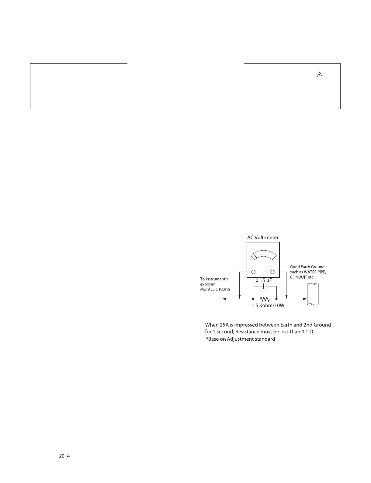
Leakage Current Hot Check (See below Figure)
Plug the AC cord directly into the AC outlet.
Do not use a line Isolation Transformer during this check.
Connect 1.5 K / 10 watt resistor in parallel with a 0.15 uF capacitor
between a known good earth ground (Water Pipe, Conduit, etc.)
and the exposed metallic parts.
Measure the AC voltage across the resistor using AC voltmeter
with 1000 ohms/volt or more sensitivity.
Reverse plug the AC cord into the AC outlet and repeat AC voltage
measur ements for each exposed met allic part. Any vol tage
measured must not exceed 0.75 volt RMS which is corresponds to
0.5 mA.
In case any measurement is out of the limits specified, there is
possibility of shock hazard and the set must be checked and
repaired before it is returned to the customer.
Leakage Current Hot Check circuit
Only for training and service purposes
- 3 -
LGE Internal Use OnlyCopyright © LG Electronics. Inc. All rights reserved.

SERVICING PRECAUTIONS
CAUTION: Before servicing receivers covered by this service
manual and its supplements and addenda, read and follow the
SAFETY PRECAUTIONS on page 3 of this publication.
NOTE: If unforeseen circumstances create conict between the
following servicing precautions and any of the safety precautions
on page 3 of this publication, always follow the safety precautions. Remember: Safety First.
General Servicing Precautions
1. Always unplug the receiver AC power cord from the AC power
source before;
a. Removing or reinstalling any component, circuit board
module or any other receiver assembly.
b. Disconnecting or reconnecting any receiver electrical plug
or other electrical connection.
c. Connecting a test substitute in parallel with an electrolytic
capacitor in the receiver.
CAUTION: A wrong part substitution or incorrect polarity
installation of electrolytic capacitors may result in an explosion hazard.
2. Test high voltage only by measuring it with an appropriate
high voltage meter or other voltage measuring device (DVM,
FETVOM, etc) equipped with a suitable high voltage probe.
Do not test high voltage by "drawing an arc".
3. Do not spray chemicals on or near this receiver or any of its
assemblies.
4. Unless specied otherwise in this service manual, clean
electrical contacts only by applying the following mixture to the
contacts with a pipe cleaner, cotton-tipped stick or comparable
non-abrasive applicator; 10 % (by volume) Acetone and 90 %
(by volume) isopropyl alcohol (90 % - 99 % strength)
CAUTION: This is a ammable mixture.
Unless specied otherwise in this service manual, lubrication
of contacts in not required.
5. Do not defeat any plug/socket B+ voltage interlocks with which
receivers covered by this service manual might be equipped.
6. Do not apply AC power to this instrument and/or any of its
electrical assemblies unless all solid-state device heat sinks
are correctly installed.
7. Always connect the test receiver ground lead to the receiver
chassis ground before connecting the test receiver positive
lead.
Always remove the test receiver ground lead last.
8. Use with this receiver only the test xtures specied in this
service manual.
CAUTION: Do not connect the test xture ground strap to any
heat sink in this receiver.
Electrostatically Sensitive (ES) Devices
Some semiconductor (solid-state) devices can be damaged easily by static electricity. Such components commonly are called
Electrostatically Sensitive (ES) Devices. Examples of typical ES
devices are integrated circuits and some eld-effect transistors
and semiconductor “chip” components. The following techniques
should be used to help reduce the incidence of component damage caused by static by static electricity.
1. Immediately before handling any semiconductor component or
semiconductor-equipped assembly, drain off any electrostatic
charge on your body by touching a known earth ground. Alternatively, obtain and wear a commercially available discharging wrist strap device, which should be removed to prevent
potential shock reasons prior to applying power to the unit
under test.
2. After removing an electrical assembly equipped with ES
devices, place the assembly on a conductive surface such as
aluminum foil, to prevent electrostatic charge buildup or exposure of the assembly.
3. Use only a grounded-tip soldering iron to solder or unsolder
ES devices.
4. Use only an anti-static type solder removal device. Some sol-
der removal devices not classied as “anti-static” can generate
electrical charges sufcient to damage ES devices.
5. Do not use freon-propelled chemicals. These can generate
electrical charges sufcient to damage ES devices.
6. Do not remove a replacement ES device from its protective
package until immediately before you are ready to install it.
(Most replacement ES devices are packaged with leads electrically shorted together by conductive foam, aluminum foil or
comparable conductive material).
7. Immediately before removing the protective material from the
leads of a replacement ES device, touch the protective material to the chassis or circuit assembly into which the device will
be installed.
CAUTION: Be sure no power is applied to the chassis or circuit, and observe all other safety precautions.
8. Minimize bodily motions when handling unpackaged replacement ES devices. (Otherwise harmless motion such as the
brushing together of your clothes fabric or the lifting of your
foot from a carpeted oor can generate static electricity sufcient to damage an ES device.)
General Soldering Guidelines
1. Use a grounded-tip, low-wattage soldering iron and appropriate tip size and shape that will maintain tip temperature within
the range or 500 °F to 600 °F.
2. Use an appropriate gauge of RMA resin-core solder composed
of 60 parts tin/40 parts lead.
3. Keep the soldering iron tip clean and well tinned.
4. Thoroughly clean the surfaces to be soldered. Use a mall wirebristle (0.5 inch, or 1.25 cm) brush with a metal handle.
Do not use freon-propelled spray-on cleaners.
5. Use the following unsoldering technique
a. Allow the soldering iron tip to reach normal temperature.
(500 °F to 600 °F)
b. Heat the component lead until the solder melts.
c. Quickly draw the melted solder with an anti-static, suction-
type solder removal device or with solder braid.
CAUTION: Work quickly to avoid overheating the circuit
board printed foil.
6. Use the following soldering technique.
a. Allow the soldering iron tip to reach a normal temperature
(500 °F to 600 °F)
b. First, hold the soldering iron tip and solder the strand
against the component lead until the solder melts.
c. Quickly move the soldering iron tip to the junction of the
component lead and the printed circuit foil, and hold it there
only until the solder ows onto and around both the component lead and the foil.
CAUTION: Work quickly to avoid overheating the circuit
board printed foil.
d. Closely inspect the solder area and remove any excess or
splashed solder with a small wire-bristle brush.
Only for training and service purposes
- 4 -
LGE Internal Use OnlyCopyright © LG Electronics. Inc. All rights reserved.

IC Remove/Replacement
Some chassis circuit boards have slotted holes (oblong) through
which the IC leads are inserted and then bent at against the circuit foil. When holes are the slotted type, the following technique
should be used to remove and replace the IC. When working with
boards using the familiar round hole, use the standard technique
as outlined in paragraphs 5 and 6 above.
Removal
1. Desolder and straighten each IC lead in one operation by
gently prying up on the lead with the soldering iron tip as the
solder melts.
2. Draw away the melted solder with an anti-static suction-type
solder removal device (or with solder braid) before removing
the IC.
Replacement
1. Carefully insert the replacement IC in the circuit board.
2. Carefully bend each IC lead against the circuit foil pad and
solder it.
3. Clean the soldered areas with a small wire-bristle brush.
(It is not necessary to reapply acrylic coating to the areas).
"Small-Signal" Discrete Transistor
Removal/Replacement
1. Remove the defective transistor by clipping its leads as close
as possible to the component body.
2. Bend into a "U" shape the end of each of three leads remaining on the circuit board.
3. Bend into a "U" shape the replacement transistor leads.
4. Connect the replacement transistor leads to the corresponding
leads extending from the circuit board and crimp the "U" with
long nose pliers to insure metal to metal contact then solder
each connection.
Power Output, Transistor Device
Removal/Replacement
1. Heat and remove all solder from around the transistor leads.
2. Remove the heat sink mounting screw (if so equipped).
3. Carefully remove the transistor from the heat sink of the circuit
board.
4. Insert new transistor in the circuit board.
5. Solder each transistor lead, and clip off excess lead.
6. Replace heat sink.
Diode Removal/Replacement
1. Remove defective diode by clipping its leads as close as possible to diode body.
2. Bend the two remaining leads perpendicular y to the circuit
board.
3. Observing diode polarity, wrap each lead of the new diode
around the corresponding lead on the circuit board.
4. Securely crimp each connection and solder it.
5. Inspect (on the circuit board copper side) the solder joints of
the two "original" leads. If they are not shiny, reheat them and
if necessary, apply additional solder.
3. Solder the connections.
CAUTION: Maintain original spacing between the replaced
component and adjacent components and the circuit board to
prevent excessive component temperatures.
Circuit Board Foil Repair
Excessive heat applied to the copper foil of any printed circuit
board will weaken the adhesive that bonds the foil to the circuit
board causing the foil to separate from or "lift-off" the board. The
following guidelines and procedures should be followed whenever this condition is encountered.
At IC Connections
To repair a defective copper pattern at IC connections use the
following procedure to install a jumper wire on the copper pattern
side of the circuit board. (Use this technique only on IC connections).
1. Carefully remove the damaged copper pattern with a sharp
knife. (Remove only as much copper as absolutely necessary).
2. carefully scratch away the solder resist and acrylic coating (if
used) from the end of the remaining copper pattern.
3. Bend a small "U" in one end of a small gauge jumper wire and
carefully crimp it around the IC pin. Solder the IC connection.
4. Route the jumper wire along the path of the out-away copper
pattern and let it overlap the previously scraped end of the
good copper pattern. Solder the overlapped area and clip off
any excess jumper wire.
At Other Connections
Use the following technique to repair the defective copper pattern
at connections other than IC Pins. This technique involves the
installation of a jumper wire on the component side of the circuit
board.
1. Remove the defective copper pattern with a sharp knife.
Remove at least 1/4 inch of copper, to ensure that a hazardous
condition will not exist if the jumper wire opens.
2. Trace along the copper pattern from both sides of the pattern
break and locate the nearest component that is directly connected to the affected copper pattern.
3. Connect insulated 20-gauge jumper wire from the lead of the
nearest component on one side of the pattern break to the
lead of the nearest component on the other side.
Carefully crimp and solder the connections.
CAUTION: Be sure the insulated jumper wire is dressed so the
it does not touch components or sharp edges.
Fuse and Conventional Resistor
Removal/Replacement
1. Clip each fuse or resistor lead at top of the circuit board hollow
stake.
2. Securely crimp the leads of replacement component around
notch at stake top.
Only for training and service purposes
- 5 -
LGE Internal Use OnlyCopyright © LG Electronics. Inc. All rights reserved.
SPECIFICATION
NOTE : Specifications and others are subject to change without notice for improvement
.
1. Application range
This specification is applied to the LED TV used LC43B
chassis.
2. Requirement for Test
Each part is tested as below without special appointment.
1) Temperature: 25 °C ± 5 °C(77 °F ± 9 °F), CST: 40 °C ± 5 °C
2) Relative Humidity: 65 % ± 10 %
3) Power Voltage
: Standard input voltage (AC 100-240 V~, 50/60 Hz)
* Standard Voltage of each products is marked by models.
4) Specification and performance of each parts are followed
ea ch dra w ing a n d spec ifica tion b y part n umber i n
accordance with BOM.
5) The receiver must be operated for about5 minutes prior to
the adjustment.
3. Test method
1) Performance: LGE TV test method followed
2) Demanded other specification
- Safety : CE, IEC specification
- EMC : CE, IEC
4. Model General Specification
No. Item Specication Remarks
1. Market Hong Kong
1) PAL-DK
2) PAL-I
2. Broadcasting system
3. Channel Storage 1500EA Maximum number of storable program for ATV /DTV
4. Channel Coverage
5. Receiving system
3) NTSC-M
4) DTMB
5) DVB-C
Analog : Upper Heterodyne
Digital : COFDM, QAM
DTMB : DMB-T + ADTB-T
Digital TV
DTMB : 21~69
DVB-C : 52.5 MHz ~866MHz
Analogue TV
PAL D/K : VHF/UHF 1 ~ 69, Cable 1 ~ 47
PAL I : VHF/UHF 1 ~ 69, Cable 1 ~ 47
NTSC M : VHF/UHF 2 ~ 78, Cable 1 ~ 71
► DTMB
(Carrier, Code Rate, Constellation, Frame Header, Interleaving)
MODE : 3780, 0.4/0.6, 4/16/64QAM, PN945, 720
QPSK : 1/2, 2/3, 3/4, 5/6, 7/8
16-QAM : 1/2, 2/3, 3/4, 5/6, 7/8
64-QAM : 1/2, 2/3, 3/4, 5/6, 7/8
► DVB-C
- Symbolrate : 4.0Msymbols/s to 7.2Msymbols/s
- Modulation : 16QAM, 64-QAM, 128-QAM and 256-QAM
6. Video(Composite) Input PAL, SECAM, NTSC Rear 1EA
7. Component Input Y/Cb/Cr, Y/Pb/Pr Rear 1EA
8. HDMI Input
9. Audio Input Component, AV L/R Input
10. USB
HDMI1-DTV/DVI
HDMI2-DTV
For My Media(Movie/Photo/Music List)
and SVC
PC(HDMI version 1.4), Support HDCP
1EA(JPEG, MP3, DivX HD)
- 6 -
Only for training and service purposes
LGE Internal Use OnlyCopyright © LG Electronics. Inc. All rights reserved.
5. Component Video Input (Y, Pb, Pr)
No. Specication H-freq(kHz) V-freq(Hz) Porposed
Resolution H-freq(kHz) V-freq(Hz)
1. 720×480 15.73 60.00 SDTV, DVD 480i
2. 720×480 15.63 59.94 SDTV, DVD 480i
3. 720×480 31.47 59.94 480p
4. 720×480 31.50 60.00 480p
5. 720×576 15.625 50.00 SDTV, DVD 625 Line
6. 720×576 31.25 50.00 HDTV 576p
7. 1280×720 45.00 50.00 HDTV 720p
8. 1280×720 44.96 59.94 HDTV 720p
9. 1280×720 45.00 60.00 HDTV 720p
10. 1920×1080 28.125 50.00 HDTV 1080i
11. 1920×1080 33.75 60.00 HDTV 1080i
12. 1920×1080 33.72 59.94 HDTV 1080i
13. 1920×1080 26.97 23.976 HDTV 1080p
14. 1920×1080 27.00 24 HDTV 1080p
15. 1920×1080 33.71 29.97 HDTV 1080p
16. 1920×1080 33.75 30 HDTV 1080p
17. 1920×1080 56.25 50 HDTV 1080p
18. 1920×1080 67.432 59.94 HDTV 1080p
19. 1920×1080 67.5 60 HDTV 1080p
6. HDMI Input
6.1. DTV mode
No. Resolution H-freq(kHz) V-freq.(kHz) Pixel clock(MHz) Proposed
1. 720*480 31.469 / 31.5 59.94 / 60 27.00/27.03 SDTV 480P
2. 720*576 31.25 50 54 SDTV 576P
3. 1280*720 37.500 50 74.25 HDTV 720P
4. 1280*720 44.96 / 45 59.94 / 60 74.17/74.25 HDTV 720P
5. 1920*1080 33.72 / 33.75 59.94 / 60 74.17/74.25 HDTV 1080I
6. 1920*1080 28.125 50.00 74.25 HDTV 1080I
7. 1920*1080 26.97 / 27 23.97 / 24 74.17/74.25 HDTV 1080P
8. 1920*1080 33.716/33.75 29.976/30.00 74.25 HDTV 1080P
9. 1920*1080 56.250 50 148.5 HDTV 1080P
10. 1920*1080 67.43 / 67.5 59.94 / 60 148.35/148.50 HDTV 1080P
6.2. PC mode
No. Resolution H-freq(kHz) V-freq.(Hz) Pixel clock(MHz) Proposed Remark
1. 640*350 @70Hz 31.468 70.09 25.17 EGA
2. 720*400 @70Hz 31.469 70.08 28.321 DOS
3. 640*480 @60Hz 31.469 59.940 25.175 VESA(VGA)
4. 800*600 @60Hz 37.879 60.31 40.000 VESA(SVGA)
5. 1024*768 @60Hz 48.363 60.00 65.000 VESA(XGA)
6 1152*864 @60Hz 54.348 60.053 80.002 VESA
7. 1280*1024 @60Hz 63.981 60.020 108 VESA(SXGA) FHD only
8. 1360*768 @60Hz 47.712 60.015 85.5 VESA(WXGA)
9. 1920*1080 @60Hz 67.5 60.0 148.5 WUXGA (Reduced blanking) FHD only
Only for training and service purposes
- 7 -
LGE Internal Use OnlyCopyright © LG Electronics. Inc. All rights reserved.
ADJUSTMENT INSTRUCTION
1. Application Range
This specification sheet is applied to all of the LED TV with
LC43B chassis.
2. Designation
(1) Th e adjus tme nt is acco rdi ng to the ord er whic h is
designated and which must be followed, according to the
plan which can be changed only on agreeing.
(2) Power adjustment : Free Voltage.
(3) Magnetic Field Condition: Nil.
(4) Input signal Unit: Product Specification Standard.
(5) Reserve after operation: Above 5 Minutes (Heat Run)
Temperature : at 25 °C ± 5 °C
Relative humidity : 65 ± 10 %
Input voltage : 220 V~, 60 Hz
(6) Adjustment equipments
: Color Analyzer(CA-210 or CA-110), Service remote control.
(7) Push the “IN STOP" key - For memory initialization.
Case1 : Software version up
1. After downloading S/W by USB , TV set will reboot
automatically.
2. Push “In-stop” key.
3. Push “Power on” key.
4. Function inspection
5. After function inspection, Push “In-stop” key.
Case2 : Function check at the assembly line
1. When TV set is entering on the assembly line, Push
“In-stop” key at rst.
2. Push “Power on” key for turning it on.
→ If you push “Power on” key, TV set will recover
channel information by itself.
3. After function inspection, Push “In-stop” key.
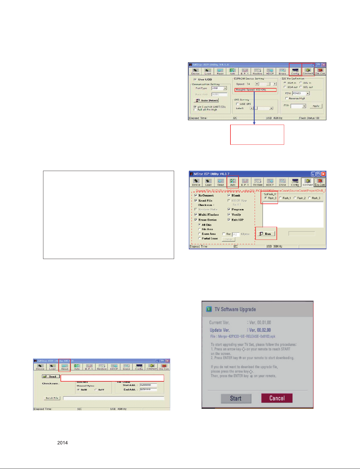
(4) Click "Connect" tab. If "Can't" is displayed, check connection
between computer, jig and set.
(2)
(3)
Please Check the Speed :
To use speed between
from 200KHz to 400KHz
(5) Click "Auto" tab and set as below.
(6) Click "Run".
(7) After downloading, check "OK" message.
(4)
filexxx.bin
(5)
(7)...........OK
(6)
3. Main PCB check process
▪ APC - After Manual-Insert, executing APC
* Boot file Download
(1) Execute ISP program "Mstar ISP Utility" and then click
"Config" tab.
(2) Set as below, and then click "Auto Detect" and check "OK"
message.
If "Error" is displayed, check connection between computer,
jig, and set.
(3) Click "Read" tab, and then load download file(XXXX.bin)
by clicking "Read"
(1)
filexxx.bin
* USB DOWNLOAD(*.epk file download)
(1) Put the USB Stick to the USB socket.
(2) Automatically detecting update file in USB Stick.
- If version of update file in USB Stick is lower, it will not
work. But version of update file is higher, USB data will be
detected automatically.
Only for training and service purposes
- 8 -
LGE Internal Use OnlyCopyright © LG Electronics. Inc. All rights reserved.
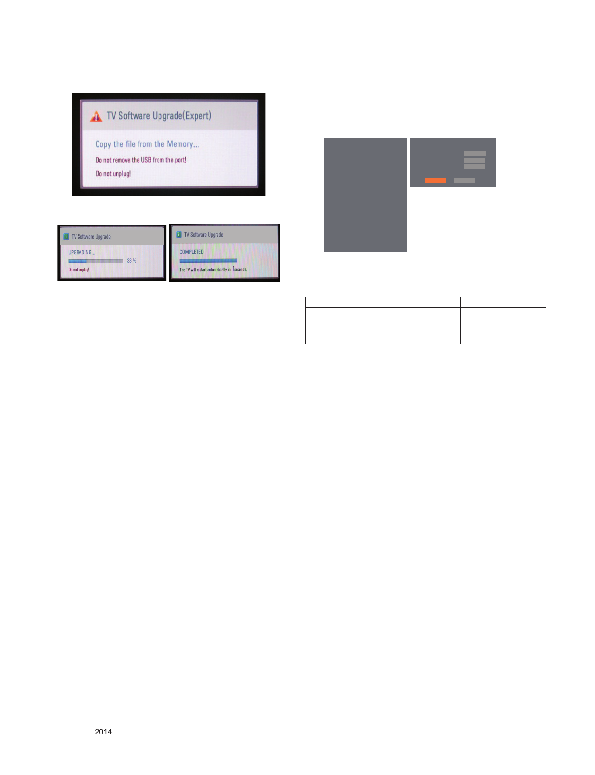
(3) Show the message "Copying files from memory".
(4) Updating is starting.
4. ADC Process
4.1. ADC
- Enter Service Mode by pushing "ADJ" key,
- Enter Internal ADC mode by pushing "►" key at "8. ADC
Calibration".
<Caution> Using "P-ONLY" key of the Adjustment remote
EZ ADJUST
0. Tool Option1
1. Tool Option2
2. Tool Option3
3. Tool Option4
4. Tool Option5
5. Tool Option Commercial
6. Country Group
7. Area Option
8. ADC Calibration ►
9. White Balance
10. 10 Point WB
11. Test Pattern
12. EDID D/L
13. Sub B/C
14. Ext. Input Adjust
control, power on TV.
ADC Calibration
ADC Comp 480i
ADC Comp 1080p
ADC Type ◄ ►
Start
Reset
OPT
NG
NG
(5) Updating Completed, The TV will restart automatically.
(6) If your TV is turned on, check your updated version and
Tool option. (explain the Tool option, next stage)
* If updated version is higher than what TV has, the TV can
lost all channel data. In this case, you have to channel
recover. If all channel data is cleared, you didn’t have a
DTV/ATV test on production line.
* After downloading, have to adjust Tool Option again.
(1) Push "IN-START" key in service remote control.
(2) Select "Tool Option 1" and push "OK" key.
(3) Punch in the number. (Each model has their number)
(4) Completed selecting Tool option.
* ADC Calibration Protocol (RS232)
NO Item CMD 1 CMD 2 Data 0
Enter
Adjust MODE
ADC adjust ADC Adjust A D 1 0
Adjust
‘Mode In’
A A 0 0
When transfer the ‘Mode In’,
Carry the command.
Automatically adjustment
(The use of a internal pattern)
Adjust Sequence
▪ aa 00 00 [Enter Adjust Mode]
▪ xb 00 40 [Component1 Input (480i)]
▪ ad 00 10 [Adjust 480i Comp1]
▪ xb 00 60 [RGB Input (1024*768)]
▪ ad 00 10 [Adjust 1024*768 RGB]
▪ aa 00 90 End Adjust mode
* Required equipment : Adjustment remote control.
4.2. Function Check
4.2.1. Check display and sound
■ Check Input and Signal items.
(1) TV
(2) AV (CVBS)
(3) COMPONENT (480i)
(4) HDMI
* Display and Sound check is executed by Remote control.
<Caution> Not to push the "INSTOP" key after completion if
the function inspection.
Only for training and service purposes
- 9 -
LGE Internal Use OnlyCopyright © LG Electronics. Inc. All rights reserved.
5. Total Assembly line process
5.1. Adjustment Preparation
▪ W/B Equipment condition
CA210: LED → CH14, Test signal: Inner pattern(80IRE)
▪ Above 5 minutes H/run in the inner pattern. ("power on" key
of Adjustment remote control)
* The spec of color temperature and coordinate.
5.1.1. W/B adj. Objective & How-it-works
(1) Objective: To reduce each Panel’s W/B deviation
(2) How-it-works: When R/G/B gain in the OSD is at 192, it
means the panel is at its Full Dynamic Range.
In order to prevent saturation of Full Dynamic range and
data, one of R/G/B is fixed at 192, and the other two is
lowered to find the desired value.
(3) Adj. condition: normal temperature
- Surrounding Temperature: 25 ± 5 °C
- Warm-up time: About 5 Min
- Surrounding Humidity: 20% ~ 80%
- Before White balance adjustment, Keep power on status,
don’t power off
* If Model is POLA model
Case : Cool Mode
• Purpose : Adjust the color temperature to reduce the
deviation of the module color temperature.
• Pr in ciple : To adjust the white bala nce without the
saturation, Fix the G gain to 172 (default data) and
change the others ( R/B Gain ).
• Adjustment mode : mode - Cool
Case : Medium / Warm Mode
• Purpose : Adjust the color temperature to reduce the
deviation of the module color temperature.
• Pr in ciple : To adjust the white bala nce without the
saturation, Fix the one of R/G/B gain to 192 (default
data) and decrease the others.
• Adjustment mode : Two modes - Medium / Warm
Mode Color Temp Color coordinate Remark
Cool (C50) 13,000 K
Medium(0) 9,300 K
Warm(W50) 6,500 K
X=0.271 (±0.002)
Y=0.270 (±0.002)
X=0.286 (±0.002)
Y=0.289 (±0.002)
X=0.313 (±0.002)
Y=0.329 (±0.002)
<Test Signal>
- Inner pattern
for W/B adjust
- External white
pattern(80IRE,
204gray)
* W/B Table( Netcast4.0 Model)
CA210 : CH 14, Test signal : Inner pattern (80IRE)
Normal line - Standard color coordinate and temprature using
CA-1000(by H/R time)
Aging
NC4.0
1 0-2 282 289 297 308 324 348
2 3-5 281 287 296 306 323 346
3 6-9 279 284 294 303 321 343
4 10-19 277 280 292 299 319 339
5 20-35 275 277 290 296 317 336
6 36-49 274 274 289 293 316 333
7 50-79 273 272 288 291 315 331
8 80-119 272 271 287 290 314 330
9 Over 120 271 270 286 289 313 329
NC4.0
1 0-5 280 285 294 308 319 340
2 6-10 276 280 290 303 315 335
3 11-20 272 275 286 298 311 330
4 21-30 269 272 283 295 308 327
5 31-40 267 268 281 291 306 323
6 41-50 266 265 280 288 305 320
7 51-80 265 263 279 286 304 318
8 81-119 264 261 278 284 303 316
9 Over 120 264 260 278 283 303 315
* When Model produce in Gumi Factory at Winter(Jan,Feb)
NC4.0
1 0-5 286 295 301 314 328 354
2 6-10 284 290 299 309 326 349
3 11-20 282 287 297 306 324 346
4 21-30 279 283 294 302 321 342
5 31-40 276 278 291 297 318 337
6 41-50 274 275 289 294 316 334
7 51-80 273 272 288 291 315 331
8 81-119 272 271 287 290 314 330
9 Over 120 271 270 286 289 313 329
time
(Min)
Aging chamber line - Standard color coordinate and temprature
using CA-1000(by H/R time)
Aging
time
(Min)
Normal line
Aging
time
(Min)
Cool Medium Warm
x y x y x y
271 270 286 289 313 329
Cool Medium Warm
x y x y x y
271 270 285 293 313 329
Cool Medium Warm
x y x y x y
271 270 286 289 313 329
Only for training and service purposes
- 10 -
* AUO, Sharp, CSOT use Model(If Cool spec 13000K)
NC4.0 Cool Medium Warm
x y x y x y
spec 271 270 286 289 313 329
target 278 280 293 299 320 339
LGE Internal Use OnlyCopyright © LG Electronics. Inc. All rights reserved.
* Connecting picture of the measuring instrument
(On Automatic control)
Inside Pattern is used when W/B is controlled. Connect to
auto controller or push Adjustment Remote control POWER
ON → Enter the mode of White-Balance, the pattern will
come out.
Full White Pattern
RS-232C Communication
CA-210
COLOR
ANALYZER
TYPE : CA-210
* Auto-control interface and directions
(1) Adjust in the place where the influx of light like floodlight
around is blocked. (Illumination is less than 10 lux).
(2) Adhere closely the Color analyzer(CA210) to the module
less than 10 cm distance, keep it with the surface of the
Module and Color analyzer's prove vertically.(90°(± 2.5°))
(3) Aging time
- After aging start, keep the power on (no suspension of
power supply) and heat-run over 5 minutes.
- Using ‘no signal’ or ‘full white pattern’ or the others,
check the back light on.
▪ Auto adjustment Map(RS-232C)
RS-232C COMMAND
[CMD ID DATA]
Wb 00 00 White Balance Start
Wb 00 ff White Balance End
RS-232C COMMAND
[CMD ID DATA]
MIN
Cool Mid Warm Cool Mid Warm
R Gain jg Ja jd 00 172 192 192 192
G Gain jh Jb je 00 172 192 192 192
B Gain ji Jc jf 00 192 192 172 192
R Cut 64 64 64 128
G Cut 64 64 64 128
B Cut 64 64 64 128
CENTER
(DEFAULT)
MAX
* Manual W/B process using adjust Remote control.
■ Color Temperature : COOL, Medium, Warm
■ One of R Gain/ G Gain/ B Gain should be kept on 0xC0,
and adjust other two lower than C0. (when R/G/B Gain are
all C0, it is the FULL Dynamic Range of Module)
■ After enter Service Mode by pushing “ADJ” key,
■ Enter White Balance by pushing “►” key at “9. White
Balance”.
EZ ADJUST
0. Tool Option1
1. Tool Option2
2. Tool Option3
3. Tool Option4
4. Tool Option5
5. Tool Option Commercial
6. Country Group
7. Area Option
8. ADC Calibration
9. White Balance
10. 20 Point WB
11. Test Pattern
12 EDID D/L
13. Sub B/C
14. V-com
15. Ext. Input Adjust
■ For manual adjustment, it is also possible by the following
sequence.
(1) Set TV in Adj. mode using POWER ON
(2) Zero Calibrate the probe of Color Analyzer, then place it
on the center of LCD module within 10cm of the surface
(3) Press ADJ key → EZ adjust using adj. R/C → 8. White-
Balance then press the cursor to the right (KEY►).
When KEY(►) is pressed 206 Gray internal pattern will
be displayed.
(4) Adjust Cool modes
1) Fix the one of R/G/B gain to 192 (default data) and
decrease the others. (If G gain is adjusted over 172
and R and B gain less than 192 , Adjust is O.K.)
2) If G gain is less than 172, Increase G gain by up to
172, and then increase R gain and G gain same
amount of increasing G gain.
3) If R gain or B gain is over 255, readjust G gain less
than 172, Conform to R gain is 255 or B gain is 255
(5) Adjust two modes (Medium/Warm) Fix the one of R/G/B
gain to 192 (default data) and decrease the others.
(6) Adj. is completed, Exit adjust mode using “EXIT” key on
Remote control.
▪ If internal pattern is not available, use RF input In EZ Adj.
menu
9. White Balance, you can select one of 2 Test-pattern:
ON, OFF. Default is inner (ON).
By selecting OFF, you can adjust using RF signal in 206
Gray pattern.
Whit Balance
Color Temp. ◄ ►
R-Gain
G-Gain
B-Gain
R-Cut
G-Cut
B-Cut
Test-Pattern
Backlight
Reset To Set
Cool
172
192
192
64
64
64
ON
100
Only for training and service purposes
- 11 -
LGE Internal Use OnlyCopyright © LG Electronics. Inc. All rights reserved.
* CASE Cool
First adjust the coordinate far away from the target
value(x, y).
1) x, y > target
i) Decrease the R, G.
2) x, y < target
i) First decrease the B gain,
ii) Decrease the one of the others.
3) x > target, y < target
i) First decrease B, so make y a little more than the
target.
ii) Adjust x value by decreasing the R.
4) x < target, y > target
i) First decrease B, so make x a little more than the
target.
ii) Adjust x value by decreasing the G.
5.2. DDC EDID Write (RGB 128Byte)
■ Connect D-sub Signal Cable to D-Sub Jack.
■ Write EDID DATA to EEPROM(24C02) by using DDC2B
protocol.
■ Check whether written EDID data is correct or not.
* For SVC main Assembly, EDID have to be downloaded to
Insert Process in advance.
5.3. DDC EDID Write (HDMI 256Byte)
■ Connect HDMI Signal Cable to HDMI Jack.
■ Write EDID DATA to EEPROM(24C02) by using DDC2B
protocol.
■ Check whether written EDID data is correct or not.
* For SVC main Assembly, EDID have to be downloaded to
Insert Process in advance.
How to adjust
1) If G gain is adjusted over 172 and R gain and B gain
less than 192, Adjust is O.K.
2) If G gain is less than 172, increase G gain by up to
172, and then increase R gain and B gain same
amount of increasing G gain.
3) If R gain or B gain is over 255, Readjust G gain less
than 172, Conform to R gain is 255 or B gain is 255.
* CASE Medium / Warm
First adjust the coordinate far away from the target
value(x, y).
1) x, y > target
i) Decrease the R, G.
2) x, y < target
i) First decrease the B gain,
ii) Decrease the one of the others.
3) x > target, y < target
i) First decrease B, so make y a little more than the
target.
ii) Adjust x value by decreasing the R
4) x < target, y > target
i) First decrease B, so make x a little more than the
target.
ii) Adjust x value by decreasing the G
* After You finish all adjustments, Press “In-start” button
and compare Tool option and Area option value with its
BOM, if it is correctly same then unplug the AC cable.
If it is not same, then correct it same with BOM and
unplug AC cable.
For correct it to the model’s module from factory JIG
model.
* Push the “IN-STOP KEY” after completing the function
inspection.
5.4. EDID DATA
1) All Data : HEXA Value
2) Changeable Data :
*: Serial No : Controlled / Data:01
**: Month : Controlled / Data:00
***: Year : Controlled
****: Check sum
- Auto Download
■ After enter Service Mode by pushing “ADJ” key,
■ Enter EDID D/L mode.
■ Enter “START” by pushing “OK” key.
* Caution : Never connect HDMI & D-sub Cable when EDID
downloaded
* Edid data and Model option download (RS232)
Enter download
Mode
EDID data and
Model option
download
EZ ADJUST
0. Tool Option1
1. Tool Option2
2. Tool Option3
3. Tool Option4
4. Tool Option5
5. Tool Option Commercial
6. Country Group
7. Area Option
8. ADC Calibration
9. White Balance
10. 20 Point WB
11. Test Pattern
12. EDID D/L ►
13. Sub B/C
14. V-Com
NO Item CMD 1 CMD 2 Data 0
Download
‘Mode In’
ADC Adjust A E 00 10
A A 0 0
EDID D/L
HDMI1 OK
HDMI2 OK
Start
Reset
When transfer the ‘Mode In’,
Carry the command.
Automatically adjustment
(The use of a internal pattern)
Only for training and service purposes
- 12 -
LGE Internal Use OnlyCopyright © LG Electronics. Inc. All rights reserved.
- Manual Download
[Caution]
* Use the proper signal cable for EDID Download
- Analog EDID : Pin3 exists
- Digital EDID : Pin3 exists
- Never connect HDMI & D-sub Cable at the same time.
- Use the proper cables below for EDID Writing.
- Download HDMI1/2/3 separately because each EDID data is
different.
For HDMI EDID
DVI-D to HDMI or HDMI to HDMI
No. Item Condition Hex Data
1 Manufacturer ID GSM 1E6D
2 Version Digital : 1 01
3 Revision Digital : 3 03
(1) EDID Data
- FHD 8BIT HDMI EDID DATA
0 1 2 3 4 5 6 7 8 9 A B C D E F
0 00 FF FF FF FF FF FF 00 1E 6D a b
10 c 01 03 80 A0 5A 78 0A EE 91 A3 54 4C 99 2 6
20 0F 50 54 A1 08 00 31 40 45 4 0 61 40 71 4 0 81 80
30 01 01 01 01 01 01 02 3A 80 18 71 38 2D 40 58 2C
40 45 00 A0 5A 0 0 00 00 1E 66 21 50 B 0 51 00 1B 30
50 40 70 36 00 A0 5A 00 00 0 0 1E 00 00 00 FD 00 3A
60 3E 1E 53 10 00 0A 20 20 20 20 20 20 d
70 d 01 e
80 02 03 22 F1 4E 10 9F 04 13 05 14 03 02 12 20 21
90 22 15 01 26 15 07 50 09 57 07 f
A0 f 01 1D 80 18 71 1C 16 20 58 2C 25 00 20 C2
B0 31 00 00 9E 01 1D 00 72 51 D0 1E 20 6E 28 5 5 00
C0 20 C2 31 00 00 1E 02 3A 80 18 71 38 2D 40 58 2C
D0 45 00 A0 5A 00 00 00 1E 01 1D 00 BC 52 D0 1E 20
E0 B8 28 55 40 C4 8E 21 00 00 1E 00 00 00 00 00 00
F0 00 00 00 00 00 00 00 00 00 00 00 00 00 00 00 e
- HD HDMI EDID data (2D Model)
0 1 2 3 4 5 6 7 8 9 A B C D E F
0 00 FF FF FF FF FF FF 00 1E 6D a b
10 c 01 03 80 A0 5A 78 0A EE 91 A3 54 4C 99 2 6
20 0F 50 54 A1 08 00 31 40 45 4 0 61 40 71 4 0 01 01
30 01 01 01 01 01 01 66 21 50 B0 51 0 0 1B 30 40 70
40 36 00 40 84 63 0 0 00 1E 6 4 19 00 40 41 00 26 30
50 18 88 03 06 40 8 4 63 00 00 18 00 0 0 00 FD 0 0 3A
60 3E 1E 53 10 00 0A 20 20 20 20 20 20 d
70 d 01 e
80 02 03 22 F1 4E 10 1F 04 93 05 14 03 02 12 20 21
90 22 15 01 26 15 07 50 09 57 07 f
A0 80 1E 01 1D 80 18 71 1C 16 20 58 2C 25 00 A0 5A
B0 00 00 00 9E 01 1D 00 72 51 D0 1E 20 6E 28 5 5 00
C0 20 C2 31 00 00 1E 8C 0A D0 8A 20 E0 2D 10 10 3E
D0 96 00 A0 5A 00 00 00 18 02 3A 80 18 71 38 2D 40
E0 58 2C 45 00 A0 5A 00 00 00 1E 00 00 00 00 00 00
F0 00 00 00 00 00 00 00 00 00 00 00 00 00 00 00 e
(2) Detail EDID Options are below
a. Product ID
Model Name HEX EDID Table DDC Function
HD/FHD Model 0001 01 00 Analog/Digital
b. Serial No: Controlled on production line.
c. Month, Year: Controlled on production line:
ex) Week : '01' -> '01'
Year : '2012' -> '16' fix
d. Model Name(Hex):
cf) TV set’s model name in EDID data is below.
MODEL NAME MODEL NAME(HEX)
LG TV 00 00 00 FC 00 4C 47 20 54 56 0A 20 20 20 20 20 20 20 (LG TV)
e. Checksum: Changeable by total EDID data.
EDID C/S data
Check Sum
(Hex)
FHD-8BIT
HDMI
Block 0 41 41 75
Block 1
25 (HDMI1) DE (HDMI1) 5B (HDMI1)
15 (HDMI2) CE (HDMI2) 4B (HDMI2)
FHD-10BIT
HDMI
HDMI
5.5. Outgoing condition Configuration
■ When pressing IN-STOP key by Service remote control,
Red LED are blinked alternatively. And then automatically
turn off. (Must not AC power OFF during blinking)
5.6. GND and HI-POT Test
5.5.1. GND & HI-POT auto-check preparation
(1) Check the POWER CABLE and SIGNAL CABE insertion
condition.
5.6.2. GND & HI-POT auto-check
(1) Pallet moves in the station.(POWER CORD / AV CORD is
tightly inserted)
(2) Connect the AV JACK Tester.
(3) Controller (GWS103-4) on.
(4) GND Test (Auto)
- If Test is failed, Buzzer operates.
- If Test is passed, execute next process(Hi-pot test).
(Remove A/V CORD from A/V JACK BOX)
(5) HI-POT test (Auto)
- If Test is failed, Buzzer operates.
- If Test is passed, GOOD Lamp on and move to next
process automatically.
5.6.3. Checkpoint
(1) Test voltage
1) 3 Poles
- GND: 1.5 KV/min at 100 mA
- SIGNAL: 3 KV/min at 100 mA
2) 2 Poles
- SIGNAL: 3 KV/min at 100 mA
(2) TEST time: 1 second
(3) TEST POINT
1) 3 Poles
- GND Test = POWER CORD GND and SIGNAL
CABLE GND.
- Hi-pot Test = POWER CORD GND and LIVE & NEUTRAL.
2) 2 Poles
- Hi-pot Test = Accessible Metal and LIVE & NEUTRAL.
(4) LEAKAGE CURRENT: At 0.5 mArms
HD
Only for training and service purposes
- 13 -
LGE Internal Use OnlyCopyright © LG Electronics. Inc. All rights reserved.
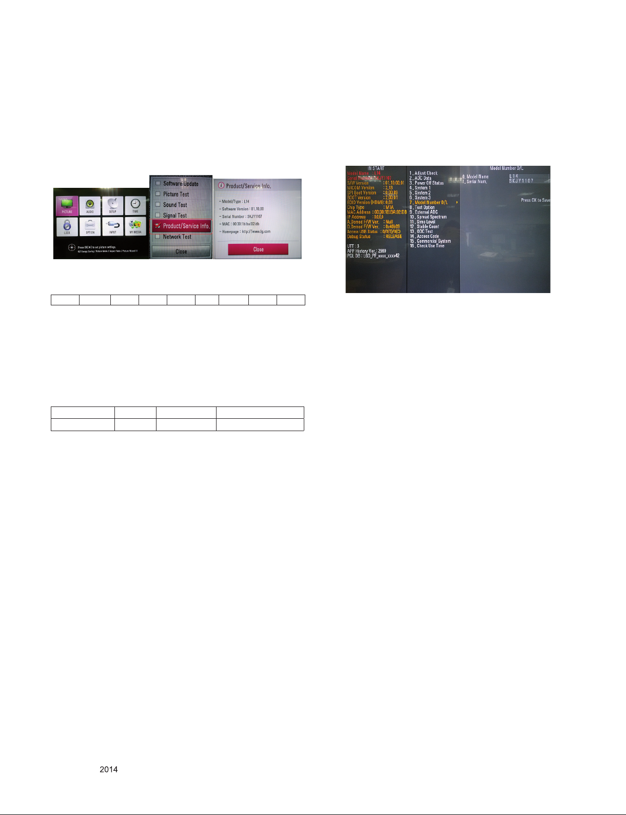
6. Model name & Serial No. download
■ Press “Power on” key of service remote control
(Baud rate : 115200 bps)
■ Connect USB to RS232 cable at USB Jack.
■ Write model name and serial number.
■ Must check the model name and serial number at the
Product/Se rvice Info . (menu key → red key → select
Product/Service info)
6.1. Signal TABLE
CMD LENGTH ADH ADL DATA_1 . . . Data_n CS DELAY
CMD : A0h
LENGTH : 85~94h (1~16 bytes)
ADH : EEPROM Sub Address high (00~1F)
ADL : EEPROM Sub Address low (00~FF)
Data : Write data
CS : CMD + LENGTH + ADH + ADL + Data_1 +...+ Data_n
Delay : 20ms
* Manual Download(Model Name and Serial Number)
If the TV set is downloaded by OTA or Service man, sometimes
model name or serial number is initialized.(Not always)
There is impossible to download by bar code scan, so It need
Manual download.
1) Press the "Instart" key of Adjustment remote control.
2) Go to the menu "6.Model Number D/L" like below photo.
3) Input the Factory model name or Serial number like photo.
4) Check the model name Instart menu. → Factory name displayed.
5) Check the Product/Service Info.(Menu Key → Red Key →
Select Product/Service Info.) → Buyer model displayed.
6.2. Comand Set
Adjust mode CMD(hex) LENGTH(hex) Description
EEPROM WRITE A0h 84h+n n-bytes Write (n = 1~16)
* Description
FOS Default write : <7mode data> write
Vtotal, V_Frequency, Sync_Polarity, Htotal, Hstart, Vstart, 0,
Phase
Data write : Model Name and Serial Number write in EEPROM,.
6.3. Method & notice
(1) Serial number D/L is using of scan equipment.
(2) Set tin g of scan eq uip men t oper ate d by Manufactu rin g
Technology Group.
(3) Serial number D/L must be conformed when it is produced in
production line, because serial number D/L is mandatory by
D-book 4.0.
Only for training and service purposes
- 14 -
LGE Internal Use OnlyCopyright © LG Electronics. Inc. All rights reserved.
BLOCK DIAGRAM
IC1300
IC104
(8Mbit)
Serial Flash
SPI_SCK/SDI/SDO/CS
(256Kbit)
System EEPROM
I2C_SCL/SDA
SPK_L
SPK_R
30P HD LVDS wafer
(P1801)
51P FHD LVDS wafer
(P1800)
(P4600)
(IC5600)
24M
X-tal
TAS5733
AUD_LRCH,
AMP_SCL/SDA
AUD_MASTER_CLK,
AUD_LRCK, AUD_SCK
Connector
KEY1/2, LED_R, IR
RXA0+/-~RXA4+/ -, RXACK+/ -
RXB0+/-~RXB4+/ -, RXBCK+/ -
(IC101)
Main SOC
M1A -256MB Built-in
USB1_OCP/CTL
AVDD5V_MHL,MHL_OCP
TPS65282
SIDE_USB_DM/DP
+5V_USB
5V_HDMI_4
USB
(JK700)
SIDE
PCM_A[0:7]
NAND FLASH
IC102 (1Gbit)
H27U1G8F2CTR-BC
TC74LCX244FT
MHL_CD_SENSE
CK+/-, D0+/-, D1+/-, D2+/-,_HDMI4, DDC_SCL/SDA_4, HDMI_CEC
Buffer
PCM_A[8:14]
TS_DATA[0:7]
PCM_DATA[0:7]
SIF
FE_TS_DATA[8]
TU_SCL / SDA
CI Slot(P1900)
(JK801)
HDMI2(MHL)
CVBS
SPDIF_OUT
DDC_SCL/SDA_2, HDMI_CEC
CK+/-, D0+/-, D1+/-, D2+/-_HDMI2
HDMI1
(JK800)
(JK1001)
SPDIF(Optic)
REAR
COMP2_L/R_IN
COMP2_Y+/AV_CVBS_IN, COMP2_Pb+/Pr+
(JK2802)
COMPONENT
Only for training and service purposes
- 15 -
LGE Internal Use OnlyCopyright © LG Electronics. Inc. All rights reserved.
400
410
EXPLODED VIEW
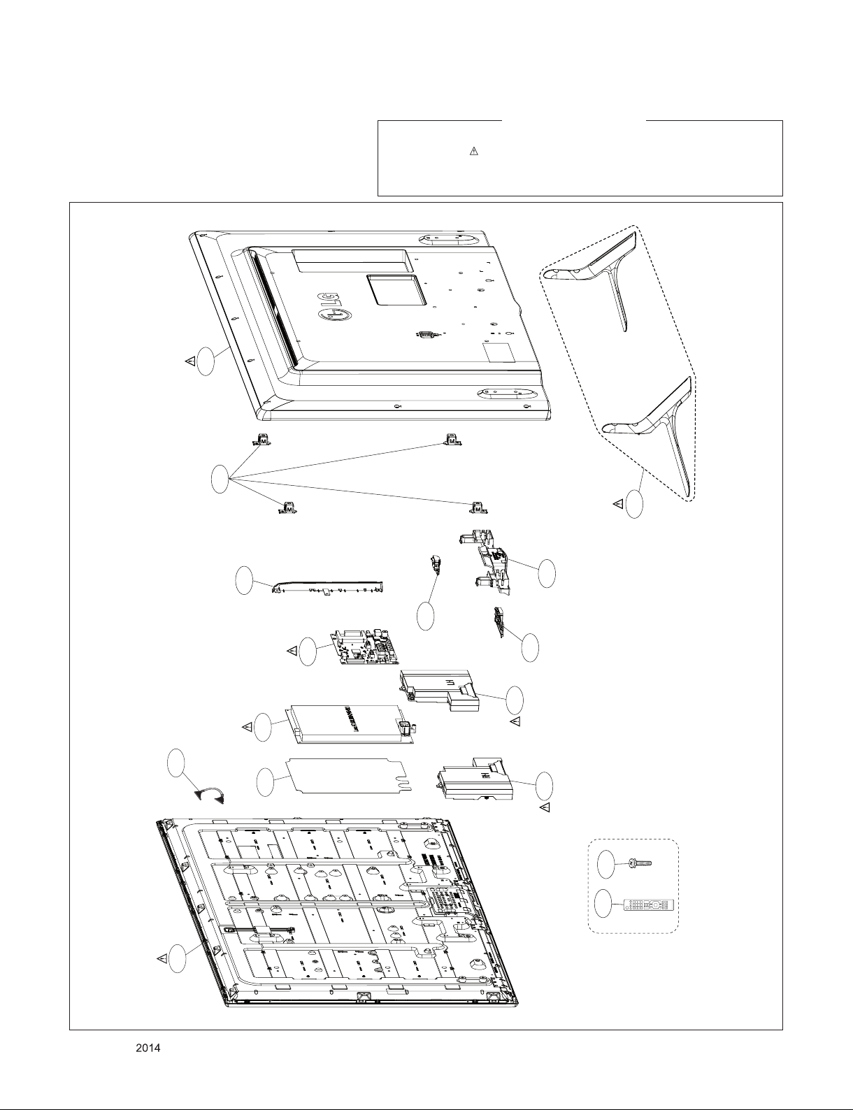
IMPORTANT SAFETY NOTICE
Many electrical and mechanical parts in this chassis have special safety-related characteristics. These
parts are identified by in the Schematic Diagram and EXPLODED VIEW.
It is essenti al that these special safety parts should be replac ed with the same compo nents as
recommended in this manual to prevent X-RADIATION, Shock, Fire, or other Hazards.
Do not modify the original design without permission of manufacturer.
900
521
310
500
540
501
121
530
LV1
820
120
A10
Set + Stand
A2
200
Only for training and service purposes
- 16 -
LGE Internal Use OnlyCopyright © LG Electronics. Inc. All rights reserved.
L14 POWER BLOCK (POWER DETECT 2)
Copyright © 2014 LG Electronics. Inc. All rights reserved.
Only for training and service purposes
LGE Internal Use Only
FROM LIPS or POWER B/D
+3.5V_ST
OPT
R400
10K
R402
R401
10K
C407
10uF
2012
10V
10K
+3.5V_POWER_DET
L400
CB2012PK501T
C400
+24V_CAP
C432
4.7uF
3216
+12V_CAP
C433
4.7uF
3216
RL_ON
+3.5V_ST
+24V
+12V
1uF
10V
1005
50V
16V
OPT
B
+3.5V_ST
R406
10K
R404
4.7K
C
Q400
MMBT3904(NXP)
E
R456
ZD400
5V
MLB-201209-0120P-N2
C401
0.1uF
50V
MLB-201209-0120P-N2
C402
0.1uF
16V
Q401
MMBT3906(NXP)
1
OPT
0
L401
CB2012PK501T
L402
L403
2
R455
3
0
ZD404
+1.5V_DDR
+3.3V_Normal
L409
BLM18PG121SN1D
C426
10uF
AZ1117EH-ADJTRG1
10V
1.3A
OPT
R412
33K
+3.3V_Normal
R420
1K
5V
PWR ON
3.5V
3.5V
GND
24V
GND
12V
12V
GND
P401
SMAW200-H18S5
1
2
3
4
5
6
7
8
10
9
11
12
13
14
15
16
17
18
19
.
DRV ON
PDIM#1
3.5V
PDMI#2
24V
GND
12V
NC
GND
R419
100
PWM_DIM_PULL_DOWN
Vout=1.25*(1+R2/R1)+Iadj*R2
+1.5V_DDR
IC404
ADJ/GND
OUTIN
R449
1K
1/16W
1%
R450
200
1/16W
1%
R1
R2
L411
CB2012PK501T
R453
0
C431
10uF
10V
ZD403
2.5V
C
B
E
Q402
MMBT3904(NXP)
R424
3.9K
+3.5V_ST
R426
10K
R425
10K
PWM2_2CH_POWER
R423
100
OPT
R467
1K
INV_CTL
PWM_DIM
PWM1
C415
0.1uF
C413
0.1uF
R457
8.2K
16V
OPT
16V
+24V
OPT
1%
R427
R428
5.1K
R430
2.7K
R431
1.2K
OPT
27K
1%
1%
1%
OPT
1%
+12V
+24V
+3.5V_POWER_DET
OPT
R432
0
5%
+3.5V_POWER_DET
OPT
R458
0
5%
Ready - Dual Power Det
* Notice
- Applying all inch models for LCD L14
- Dual Power Det is used
for detecting two kinds of voltage
+1.10V_VDDC
+1.10V_VDDC
ZD401
2.5V
+3.5V_ST
OPT
C424
0.1uF
16V
C437
0.1uF
CB2012PK501T
OPT
C436
10uF
10V
16V
C420
C421
22uF
22uF
10V
10V
RESET_IC_ROHM
BD48K28G
VDD
3
BD48K28G
VDD
3
L406
C423
50V
270pF
R435
100K
IC401
OPT
R436
100K
OPT
IC402
C414
10uF
10V
2
1
GND
2
1
GND
0.1uF
R43 9
20K
1%
R44 0
47K
1%
PD_+3.5V
R454-*1
300
5%
PD_+12V
R454
VOUT
VOUT
100 5%
POWER_DET_RESET
OPT
R437
100 5%
Detect Valtage
Power Detect +3.5V
Power Detect +12V
Power Detect +24V
C435
16V
C417
L407
0.1uF
3.6uH
16V
R1
R2
+3.5V_ST
OPT
R438
4.7K
C422
0.1uF
Power_DET
POWER_DET
VCC
VCC
Power Detect activity
Now is
Use Circuit Designator
R432, R454-*1, R438
O R430, R431, R454
R457, R454
IC403
TPS5432DDAR
BOOT
VIN
PH
GND
1
2
3
4
3A
9
THERMAL
8
7
6
5
[EP]GND
SS
EN
COMP
VSENSE
C418
0.01uF
R433
2.7K
C419
0.039uF
50V
1%
Vout=0.808*(1+R1/R2)
RESET_IC_DIODES
IC401-*1
APX803D29
3
2
1
GND
OPT
IC402-*1
APX803D29
3
2
1
GND
+3.3V_Normal
R429
10K
C416
0.33uF
16V
C434
390pF
50V
RESET
RESET
PANEL_VCC
PANEL_CTL
+3.3V_Normal
POWER_ON/OFF_1
L408
UBW2012-121F
120OHM
OPT
C425
0.1uF
25V
R441
+3.5V_ST
R443
10K
FET_NXP
Q405-*1
PMV48XP
D
S
Q406
AO3435
S
S
G
FET_Diode
Q405
DMP2130L
S
G
FET_NXP
Q406-*2
PMV48XP
D
S
G
BLM18PG121SN1D
D
C429
G
0.1uF
16V
+12V
C427
R445
10uF
33K
16V
R446
12K
B
C428
2.2uF
10V
C
Q404
MMBT3904(NXP)
E
C
Q403
MMBT3904(NXP)
E
FET_2.5V_DIODE
Q406-*1
DMP2130L
FET_2.5V_AOS
R442
10K
10K
R447
22K
R448
2.2K
R444
10K
B
PANEL_VCC
D
R451
R452
5.6K
5.6K
D
+3.3V_Normal
G
L410
C430
ZD402
22uF
5V
10V
+5V_Normal & +5V_USB with OCP
OPT
C403
100pF
50V
R408
OPT
R405
4.7K
4.7K
/VBUS_EN
(Active Low)
MHL_OCP_EN
(Active High)
+3.3V_Normal
MHL_SW_TR
MHL_SW_TR
R461
10K
MHL_SW_TR
MHL_SW_TR
R462
10K
Q407
B
R463
2.7K
C
MHL_SW_TR
E
MHL_SW_TR
Q409
MHL_SW_TR
R464
10K
MHL_SW_TR
Q408
E
B
R465
10K
B
+3.3V_Normal
OPT
R403
4.7K
MHL_5V_EN
USB1_CTL
C
MHL_5V_EN
R466
20K
C
E
R410
100K
C404
4700pF
50V
OPT
R459
0
+3.3V_Normal
R407
R409
10K
10K
COMP
ROSC
EN_SW2
EN_SW1
[EP]GND
V7V
EN
1
2
SS
3
4
TPS65282REGR
5
6
FAULT2
+12V
C405
10uF
VIN_223PGOOD
22
24
THERMAL
25
IC400
4A
7
9
8
FAULT1
SW_OUT2
USB1_OCD
/MHL_OCP_DET
C406
10uF
16V
PGND_2
VIN_1
21
10
RLIM11AGND
R415
15K
5%
OPT
R416
100K
PGND_1
19
20
18
17
16
15
14
13
12
SW_OUT1
D401
MBR230LSFT1G
C409
L405
0.047uF
4.7uH
25V
BST
LX_2
LX_1
FB
SW_IN_2
SW_IN_1
C410
5V_HDMI_4
10uF
10V
AVDD5V_MHL
R418
10
+5V_USB
30V
C408
10uF
10V
Vout=0.8*(1+R1/R2)
R422
3.3K
R421
18K
1%
R1
R2
+5V_Normal
C411
C412
82pF
22uF
50V
16V
1%
THE SYMBOL MARK OF THIS SCHEMETIC DIAGRAM INCORPORATES
SPECIAL FEATURES IMPORTANT FOR PROTECTION FROM X-RADIATION.
FIRE AND ELECTRICAL SHOCK HAZARDS, WHEN SERVICING IF IS
ESSENTIAL THAT ONLY MANUFACTURES SPECIFIED PARTS BE USED FOR
THE CRITICAL COMPONENTS IN THE SYMBOL MARK OF THE SCHEMETIC.
L14_M1A
Power_PD2
131123
4
USB (SIDE)
Copyright © 2014 LG Electronics. Inc. All rights reserved.
Only for training and service purposes
LGE Internal Use Only
USB_HDD_CAP1_10uF
C700-*1
USB_HDD_CAP1_22uF
OPT
C701
5pF
50V
OPT
ZD700
SD05
5V
OPT
C702
5pF
50V
JK700
1234
USB DO WN ST REA M
3AU 04S -3 05- ZC- (L G)
5
10uF
10V
USB_HDD_CAP2_10uF
C703-*1
USB_HDD_CAP2_22uF
C700
22uF
10V
OPT
D700
RCLAMP0502BA
10uF
10V
C703
22uF
10V
+5V_USB
OPT
C704
22uF
10V
SIDE_USB1_DM
SIDE_USB1_DP
THE SYMBOL MARK OF THIS SCHEMETIC DIAGRAM INCORPORATES
SPECIAL FEATURES IMPORTANT FOR PROTECTION FROM X-RADIATION.
FIRE AND ELECTRICAL SHOCK HAZARDS, WHEN SERVICING IF IS
ESSENTIAL THAT ONLY MANUFACTURES SPECIFIED PARTS BE USED FOR
THE CRITICAL COMPONENTS IN THE SYMBOL MARK OF THE SCHEMETIC.
L14_M1A
USB_S1
14/03/03
7
HDMI (REAR 1 / SIDE 1 MHL)
Copyright © 2014 LG Electronics. Inc. All rights reserved.
Only for training and service purposes
LGE Internal Use Only
HDMI_1
SHIELD
20
19
18
17
16
15
14
13
12
11
CK+
10
EAG59023302
JK800
9
8
7
6
5
4
3
2
1
D0-
D0_GND
D0+
D1-
D1_GND
D1+
D2-
D2_GND
D2+
5V_HDMI_2
R803
1K
R802
1.8K
VA800
ESD_HDMI1_VARISTOR
5V_DET_HDMI_2
ESD_HDMI1
R805
3.3K
VA801
ESD_HDMI1_VARISTOR
VA800-*1
1uF
10V
ESD_HDMI1_CAP
VA801-*1
1uF
10V
ESD_HDMI1_CAP
VA802
MMBT3904(NXP)
Q800
C
E
VA803
ESD_HDMI1
R808
10K
B
R809
10K
R810 100
R811 100
VA804
ESD_HDMI1
D803
1
2
3
4
5
ESD_HDMI1_IP4294
IP4294CZ10-TBR
D804
1
2
3
4
5
ESD_HDMI1_IP4294
IP4294CZ10-TBR
10
9
8
7
6
10
9
8
7
6
HPD2
DDC_SDA_2
DDC_SCL_2
HDMI_ARC
HDMI_CEC
CK-_HDMI2
CK+_HDMI2
D0-_HDMI2
D0+_HDMI2
D1-_HDMI2
D1+_HDMI2
D2-_HDMI2
D2+_HDMI2
HDMI_2 MHL
VA805
ESD_HDMI2
GND
20
HP_DET
19
5V
18
GND
17
DDC_DATA
16
DDC_CLK
15
NC
14
CE_REMOTE
13
CK-
12
CK_GND
11
CK+
10
BODY_SHIELD
20
19
HOT_PLUG_DETECT
18
VDD[+5V]
17
DDC/CEC_GND
16
SDA
15
SCL
14
RESERVED
13
CEC
12
TMDS_CLK-
11
TMDS_CLK_SHIELD
10
TMDS_CLK+
9
TMDS_DATA0-
8
TMDS_DATA0_SHIELD
7
TMDS_DATA0+
6
TMDS_DATA1-
5
TMDS_DATA1_SHIELD
4
TMDS_DATA1+
3
TMDS_DATA2-
2
TMDS_DATA2_SHIELD
1
TMDS_DATA2+
JK801-*1
DAADR019A
HDMI-2_EMI_FOOSUNG
EAG62611204
JK801
HDMI-2
9
8
7
6
5
4
3
2
1
D0-
D0_GND
D0+
D1-
D1_GND
D1+
D2-
D2_GND
D2+
5V_HDMI_4
R812
1.8K
HDMI-2
5V_DET_HDMI_4
ESD_HDMI2
VA806
R813
3.3K
HDMI-2
VA807
5.6V
OPT
ESD_HDMI2
VA808
ESD_HDMI2
VA809
HDMI-2
R814
33
HDMI-2
R815 100
R816 100
HDMI-2
VA810
ESD_HDMI2
VA811
ESD_HDMI2
1
2
3
4
5
ESD_HDMI2_IP4294
IP4294CZ10-TBR
1
2
3
4
5
ESD_HDMI2_IP4294
IP4294CZ10-TBR
C800
0.047uF
25V
HDMI-2
D805
D806
10
9
8
7
6
10
9
8
7
6
R817
300K
MHL Spec
HDMI-2
HPD4
DDC_SDA_4
DDC_SCL_4
HDMI_CEC
CK-_HDMI4
CK+_HDMI4
D0-_HDMI4
D0+_HDMI4
D1-_HDMI4
D1+_HDMI4
D2-_HDMI4
D2+_HDMI4
MHL_CD_SENSE
CEC
R804
A2CA1
MMBD6100
D800
100
DDC_SDA_2
DDC_SCL_2
CEC_REMOTE_S7
5V_HDMI_4
R806
2.7K
+5V_Normal
A2CA1
MMBD6100
D801
R807
2.7K
+3.5V_ST
DDC_SDA_4
DDC_SCL_4
A2CA1
MMBD6100
D802
HDMI_CEC
5V_HDMI_2
R800
2.7K
+5V_Normal
R801
2.7K
THE SYMBOL MARK OF THIS SCHEMETIC DIAGRAM INCORPORATES
SPECIAL FEATURES IMPORTANT FOR PROTECTION FROM X-RADIATION.
FIRE AND ELECTRICAL SHOCK HAZARDS, WHEN SERVICING IF IS
ESSENTIAL THAT ONLY MANUFACTURES SPECIFIED PARTS BE USED FOR
THE CRITICAL COMPONENTS IN THE SYMBOL MARK OF THE SCHEMETIC.
D803-*1
TMDS_CH1-
1
2
GND_1
3
4
5
D803-*2
1
2
3
4
5
10
9
8
7
6
10
9
8
7
6
TMDS_CH1+
TMDS_CH2-
TMDS_CH2+
ESD_HDMI1_IP4283
IP4283CZ10-TBA
ESD_HDMI1_SEMTECH
RCLAMP0524PA
NC_4
NC_3
GND_2
NC_2
NC_1
D804-*1
TMDS_CH1-
1
2
GND_1
3
4
5
D804-*2
1
2
3
4
5
10
10
9
8
7
6
TMDS_CH1+
TMDS_CH2-
TMDS_CH2+
ESD_HDMI1_IP4283
IP4283CZ10-TBA
ESD_HDMI1_SEMTECH
RCLAMP0524PA
D805-*1
NC_4
NC_3
9
GND_2
8
NC_2
7
NC_1
6
TMDS_CH1-
1
2
GND_1
3
4
5
D805-*2
1
2
3
4
5
10
10
9
8
7
6
TMDS_CH1+
TMDS_CH2-
TMDS_CH2+
ESD_HDMI2_IP4283
IP4283CZ10-TBA
ESD_HDMI2_SEMTECH
RCLAMP0524PA
NC_4
NC_3
9
GND_2
8
NC_2
7
NC_1
6
D806-*1
TMDS_CH1-
1
TMDS_CH1+
2
GND_1
3
TMDS_CH2-
4
TMDS_CH2+
5
ESD_HDMI2_IP4283
IP4283CZ10-TBA
D806-*2
1
2
3
4
5
ESD_HDMI2_SEMTECH
RCLAMP0524PA
L14_M1A
NC_4
10
NC_3
9
GND_2
8
NC_2
7
NC_1
6
10
9
8
7
6
2013/08/15
HDMI_R1_S1 8
SPDIF
Copyright © 2014 LG Electronics. Inc. All rights reserved.
Only for training and service purposes
LGE Internal Use Only
SPDIF OPTIC JACK
5.15 Mstar Circuit Application
SPDIF_OUT
+3.3V_Normal
C1001
1uF
OPT
10V
ESD Ready
SPDIF_CAP_47pF
C1002
47pF
50V
SPDIF_CAP_18pF
C1002-*1
18pF
50V
VINPUT
SPDIF_OPTIC
JST1223-001
GND
VCC
JK1001
1
2
3
Fiber Optic
4
FIX_POLE
THE SYMBOL MARK OF THIS SCHEMETIC DIAGRAM INCORPORATES
SPECIAL FEATURES IMPORTANT FOR PROTECTION FROM X-RADIATION.
FIRE AND ELECTRICAL SHOCK HAZARDS, WHEN SERVICING IF IS
ESSENTIAL THAT ONLY MANUFACTURES SPECIFIED PARTS BE USED FOR
THE CRITICAL COMPONENTS IN THE SYMBOL MARK OF THE SCHEMETIC.
NC5_L14
SPDIF
2013/10/29
10
R12011K1%
Copyright © 2014 LG Electronics. Inc. All rights reserved.
Only for training and service purposes
LGE Internal Use Only
DDR_EXT
DDR_EXT
R1202 1K1%
DDR_EXT
C1201 0.1uF
DDR_EXT
C1202 1000pF
A-MVREFDQ
+1.5V_DDR+1.5V_DDR
DDR_EXT
R1204 1K 1%
DDR_EXT
R1205 1K 1%
DDR_EXT
C1213 0.1uF
1000pF
DDR_EXT
C1214
A-MVREFCA
Option : Ripple Check !!!
+1.5V_DDR
C1217
C1216
10uF 10V
OPT
OPT
0.1uF
C1218
OPT
0.1uF
C1219
OPT
+1.5V_DDR
1uF
1uF
1uF
1uF
C1222
OPT
C1223
OPT
1uF
0.1uF
C1224
OPT
C1220
OPT
C1221
OPT
CLose to DDR3
DDR_1600_1G_SS
IC1201-*1
K4B1G1646G-BCK0
EAN61836301
N3
A0
P7
A1
P3
A2
N2
A3
P8
A4
P2
A5
R8
A6
R2
A7
T8
A8
R3
A9
L7
A10/AP
R7
A11
N7
A12/BC
T3
A13
M7
NC_5
M2
BA0
N8
BA1
M3
BA2
J7
CK
K7
CK
K9
CKE
L2
CS
K1
ODT
J3
RAS
K3
CAS
L3
WE
T2
RESET
F3
DQSL
G3
DQSL
C7
DQSU
B7
DQSU
E7
DML
D3
DMU
E3
DQL0
F7
DQL1
F2
DQL2
F8
DQL3
H3
DQL4
H8
DQL5
G2
DQL6
H7
DQL7
D7
DQU0
C3
DQU1
C8
DQU2
C2
DQU3
A7
DQU4
A2
DQU5
B8
DQU6
A3
DQU7
CLose to Saturn7M IC
DDR_1600_1G_HYNIX
IC1201
H5TQ1G63EFR-PBC
EAN61829003
M8
VREFCA
H1
VREFDQ
L8
240
1%
ZQ
B2
VDD_1
D9
VDD_2
G7
VDD_3
K2
VDD_4
K8
VDD_5
N1
VDD_6
N9
VDD_7
R1
VDD_8
R9
VDD_9
A1
VDDQ_1
A8
VDDQ_2
C1
VDDQ_3
C9
VDDQ_4
D2
VDDQ_5
E9
VDDQ_6
F1
VDDQ_7
H2
VDDQ_8
H9
VDDQ_9
J1
NC_1
J9
NC_2
L1
NC_3
L9
NC_4
T7
NC_6
A9
VSS_1
B3
VSS_2
E1
VSS_3
G8
VSS_4
J2
VSS_5
J8
VSS_6
M1
VSS_7
M9
VSS_8
P1
VSS_9
P9
VSS_10
T1
VSS_11
T9
VSS_12
B1
VSSQ_1
B9
VSSQ_2
D1
VSSQ_3
D8
VSSQ_4
E2
VSSQ_5
E8
VSSQ_6
F9
VSSQ_7
G1
VSSQ_8
G9
VSSQ_9
+1.5V_DDR
10V
A-MVREFCA
A-MVREFDQ
C1203 10uF
C1204 0.1uF
C1205 0.1uF
C1206 0.1uF
C1207 0.1uF
C1208 0.1uF
C1209 0.1uF
C1210 0.1uF
C1211 0.1uF
C1212 0.1uF
A-MA14
DDR_EXT
R1203
DDR_1600_2G_HYNIX_OLD
IC1201-*2
H5TQ2G63DFR-PBC
M8
VREFCA
H1
VREFDQ
L8
ZQ
B2
VDD_1
D9
VDD_2
G7
VDD_3
K2
VDD_4
K8
VDD_5
N1
VDD_6
N9
VDD_7
R1
VDD_8
R9
VDD_9
A1
VDDQ_1
A8
VDDQ_2
C1
VDDQ_3
C9
VDDQ_4
D2
VDDQ_5
E9
VDDQ_6
F1
VDDQ_7
H2
VDDQ_8
H9
VDDQ_9
J1
NC_1
J9
NC_2
L1
NC_3
L9
NC_4
T7
NC_6
A9
VSS_1
B3
VSS_2
E1
VSS_3
G8
VSS_4
J2
VSS_5
J8
VSS_6
M1
VSS_7
M9
VSS_8
P1
VSS_9
P9
VSS_10
T1
VSS_11
T9
VSS_12
B1
VSSQ_1
B9
VSSQ_2
D1
VSSQ_3
D8
VSSQ_4
E2
VSSQ_5
E8
VSSQ_6
F9
VSSQ_7
G1
VSSQ_8
G9
VSSQ_9
N3
P7
P3
N2
P8
P2
R8
R2
T8
R3
L7
R7
N7
T3
M7
M2
N8
M3
J7
K7
K9
L2
K1
J3
K3
L3
T2
F3
G3
C7
B7
E7
D3
E3
F7
F2
F8
H3
H8
G2
H7
D7
C3
C8
C2
A7
A2
B8
A3
EAN61829203
A0
A1
A2
A3
A4
A5
A6
A7
A8
A9
A10/AP
A11
A12/BC
A13
NC_5
BA0
BA1
BA2
CK
CK
CKE
CS
ODT
RAS
CAS
WE
RESET
DQSL
DQSL
DQSU
DQSU
DML
DMU
DQL0
DQL1
DQL2
DQL3
DQL4
DQL5
DQL6
DQL7
DQU0
DQU1
DQU2
DQU3
DQU4
DQU5
DQU6
DQU7
VREFCA
VREFDQ
ZQ
VDD_1
VDD_2
VDD_3
VDD_4
VDD_5
VDD_6
VDD_7
VDD_8
VDD_9
VDDQ_1
VDDQ_2
VDDQ_3
VDDQ_4
VDDQ_5
VDDQ_6
VDDQ_7
VDDQ_8
VDDQ_9
NC_1
NC_2
NC_3
NC_4
NC_6
VSS_1
VSS_2
VSS_3
VSS_4
VSS_5
VSS_6
VSS_7
VSS_8
VSS_9
VSS_10
VSS_11
VSS_12
VSSQ_1
VSSQ_2
VSSQ_3
VSSQ_4
VSSQ_5
VSSQ_6
VSSQ_7
VSSQ_8
VSSQ_9
M8
H1
L8
B2
D9
G7
K2
K8
N1
N9
R1
R9
A1
A8
C1
C9
D2
E9
F1
H2
H9
J1
J9
L1
L9
T7
A9
B3
E1
G8
J2
J8
M1
M9
P1
P9
T1
T9
B1
B9
D1
D8
E2
E8
F9
G1
G9
DDR_1600_2G_HYNIX_NEW
IC1201-*3
H5TQ2G63FFR-PBC
EAN61829204
N3
VREFCA
A0
P7
A1
P3
A2
N2
A3
VREFDQ
P8
A4
P2
A5
R8
A6
R2
A7
T8
A8
R3
A9
L7
R7
N7
T3
M7
M2
N8
M3
J7
K7
K9
L2
K1
J3
K3
L3
T2
F3
G3
C7
B7
E7
D3
E3
F7
F2
F8
H3
H8
G2
H7
D7
C3
C8
C2
A7
A2
B8
A3
VDD_1
A10/AP
VDD_2
A11
VDD_3
A12/BC
VDD_4
VDD_5
A13
VDD_6
VDD_7
NC_5
VDD_8
VDD_9
BA0
BA1
BA2
VDDQ_1
VDDQ_2
CK
VDDQ_3
CK
VDDQ_4
CKE
VDDQ_5
VDDQ_6
CS
VDDQ_7
ODT
VDDQ_8
RAS
VDDQ_9
CAS
WE
NC_1
NC_2
RESET
NC_3
NC_4
NC_6
DQSL
DQSL
VSS_1
DQSU
VSS_2
DQSU
VSS_3
VSS_4
DML
VSS_5
DMU
VSS_6
VSS_7
DQL0
VSS_8
DQL1
VSS_9
DQL2
VSS_10
DQL3
VSS_11
DQL4
VSS_12
DQL5
DQL6
DQL7
VSSQ_1
VSSQ_2
DQU0
VSSQ_3
DQU1
VSSQ_4
DQU2
VSSQ_5
DQU3
VSSQ_6
DQU4
VSSQ_7
DQU5
VSSQ_8
DQU6
VSSQ_9
DQU7
DDR_1600_2G_SS
IC1201-*4
K4B2G1646Q-BCK0
M8
H1
L8
ZQ
B2
D9
G7
K2
K8
N1
N9
R1
R9
A1
A8
C1
C9
D2
E9
F1
H2
H9
J1
J9
L1
L9
T7
A9
B3
E1
G8
J2
J8
M1
M9
P1
P9
T1
T9
B1
B9
D1
D8
E2
E8
F9
G1
G9
N3
P7
P3
N2
P8
P2
R8
R2
T8
R3
L7
R7
N7
T3
M7
M2
N8
M3
J7
K7
K9
L2
K1
J3
K3
L3
T2
F3
G3
C7
B7
E7
D3
E3
F7
F2
F8
H3
H8
G2
H7
D7
C3
C8
C2
A7
A2
B8
A3
EAN61848803
A0
A1
A2
A3
A4
A5
A6
A7
A8
A9
A10/AP
A11
A12/BC
A13
NC_5
BA0
BA1
BA2
CK
CK
CKE
CS
ODT
RAS
CAS
WE
RESET
DQSL
DQSL
DQSU
DQSU
DML
DMU
DQL0
DQL1
DQL2
DQL3
DQL4
DQL5
DQL6
DQL7
DQU0
DQU1
DQU2
DQU3
DQU4
DQU5
DQU6
DQU7
M8
VREFCA
H1
VREFDQ
L8
ZQ
B2
VDD_1
D9
VDD_2
G7
VDD_3
K2
VDD_4
K8
VDD_5
N1
VDD_6
N9
VDD_7
R1
VDD_8
R9
VDD_9
A1
VDDQ_1
A8
VDDQ_2
C1
VDDQ_3
C9
VDDQ_4
D2
VDDQ_5
E9
VDDQ_6
F1
VDDQ_7
H2
VDDQ_8
H9
VDDQ_9
J1
NC_1
J9
NC_2
L1
NC_3
L9
NC_4
T7
NC_6
A9
VSS_1
B3
VSS_2
E1
VSS_3
G8
VSS_4
J2
VSS_5
J8
VSS_6
M1
VSS_7
M9
VSS_8
P1
VSS_9
P9
VSS_10
T1
VSS_11
T9
VSS_12
B1
VSSQ_1
B9
VSSQ_2
D1
VSSQ_3
D8
VSSQ_4
E2
VSSQ_5
E8
VSSQ_6
F9
VSSQ_7
G1
VSSQ_8
G9
VSSQ_9
DDR_EXT
DDR_EXT
DDR_EXT
DDR_EXT
DDR_EXT
DDR_EXT
DDR_EXT
DDR_EXT
DDR_EXT
DDR_EXT
A10/AP
A12/BC
NC_7
NC_5
RESET
DQSL
DQSL
DQSU
DQSU
DQL0
DQL1
DQL2
DQL3
DQL4
DQL5
DQL6
DQL7
DQU0
DQU1
DQU2
DQU3
DQU4
DQU5
DQU6
DQU7
N3
A0
P7
A1
P3
A2
N2
A3
P8
A4
P2
A5
R8
A6
R2
A7
T8
A8
R3
A9
L7
R7
A11
N7
T3
M7
M2
BA0
N8
BA1
M3
BA2
J7
CK
K7
CK
K9
CKE
L2
CS
K1
ODT
J3
RAS
K3
CAS
L3
WE
T2
F3
G3
C7
B7
E7
DML
D3
DMU
E3
F7
F2
F8
H3
H8
G2
H7
D7
C3
C8
C2
A7
A2
B8
A3
A-MA0
A-MA1
A-MA2
A-MA3
A-MA4
A-MA5
A-MA6
A-MA7
A-MA8
A-MA9
A-MA10
A-MA11
A-MA12
A-MA13
A-MBA0
A-MBA1
A-MBA2
A-MCKE
A/B_DDR3_CS
A-MODT
A-MRASB
A-MCASB
A-MWEB
A-MRESETB
A-MDQSL
A-MDQSLB
A-MDQSU
A-MDQSUB
A-MDML
A-MDMU
A-MDQL0
A-MDQL1
A-MDQL2
A-MDQL3
A-MDQL4
A-MDQL5
A-MDQL6
A-MDQL7
A-MDQU0
A-MDQU1
A-MDQU2
A-MDQU3
A-MDQU4
A-MDQU5
A-MDQU6
A-MDQU7
R1207
DDR_EXT
R1208
DDR_EXT
DDR_EXT
R1206
10K
DDR_EXT
56 1%
C1215
0.01uF
50V
56 1%
A-MCKB
+1.5V_DDR
A-MCK
A-MDQSUB
A-MDQSLB
A-MDQSU
A-MDQSL
A/B_DDR3_CS
A-MA0
A-MA1
A-MA2
A-MA3
A-MA4
A-MA5
A-MA6
A-MA7
A-MA8
A-MA9
A-MA10
A-MA11
A-MA12
A-MA13
A-MA14
A-MBA0
A-MBA1
A-MBA2
A-MCK
A-MCKB
A-MCKE
A-MODT
A-MRASB
A-MCASB
A-MWEB
A-MRESETB
A-MDML
A-MDMU
A-MDQL0
A-MDQL1
A-MDQL2
A-MDQL3
A-MDQL4
A-MDQL5
A-MDQL6
A-MDQL7
A-MDQU0
A-MDQU1
A-MDQU2
A-MDQU3
A-MDQU4
A-MDQU5
A-MDQU6
A-MDQU7
R1209
240
1%
M1A_256M_UO3
IC101
LGE2132(M1A_256M)
E11
B_DDR3_A[0]
F12
B_DDR3_A[1]
D10
B_DDR3_A[2]
B10
B_DDR3_A[3]
E15
B_DDR3_A[4]
B11
B_DDR3_A[5]
F14
B_DDR3_A[6]
C11
B_DDR3_A[7]
D14
B_DDR3_A[8]
A12
B_DDR3_A[9]
F16
B_DDR3_A[10]
D13
B_DDR3_A[11]
D15
B_DDR3_A[12]
C12
B_DDR3_A[13]
E13
B_DDR3_A[14]
A9
B_DDR3_BA[0]
D16
B_DDR3_BA[1]
A10
B_DDR3_BA[2]
C13
B_DDR3_MCLK
B13
B_DDR3_MCLKZ
E17
B_DDR3_MCLKE
B8
B_DDR3_ODT
C8
B_DDR3_RASZ
B9
B_DDR3_CASZ
D11
B_DDR3_WEZ
F10
B_RESET
D12
B_DDR3_CS0
A19
B_DDR3_DQSL
B18
B_DDR3_DQSU
C16
B_DDR3_DQML
D21
B_DDR3_DQMU
C18
B_DDR3_DQSBL
C17
B_DDR3_DQSBU
A20
B_DDR3_DQL[0]
A16
B_DDR3_DQL[1]
C19
B_DDR3_DQL[2]
C15
B_DDR3_DQL[3]
C20
B_DDR3_DQL[4]
C14
B_DDR3_DQL[5]
B21
B_DDR3_DQL[6]
B15
B_DDR3_DQL[7]
F18
B_DDR3_DQU[0]
D19
B_DDR3_DQU[1]
D17
B_DDR3_DQU[2]
E21
B_DDR3_DQU[3]
E19
B_DDR3_DQU[4]
D20
B_DDR3_DQU[5]
D18
B_DDR3_DQU[6]
F20
B_DDR3_DQU[7]
E9
ZQ
M1A_128M_UO3
IC101-*1
LGE2131(M1A_128M)
E11
B_DDR3_A[0]
F12
B_DDR3_A[1]
D10
B_DDR3_A[2]
B10
B_DDR3_A[3]
E15
B_DDR3_A[4]
B11
B_DDR3_A[5]
F14
B_DDR3_A[6]
C11
B_DDR3_A[7]
D14
B_DDR3_A[8]
A12
B_DDR3_A[9]
F16
B_DDR3_A[10]
D13
B_DDR3_A[11]
D15
B_DDR3_A[12]
C12
B_DDR3_A[13]
E13
B_DDR3_A[14]
A9
B_DDR3_BA[0]
D16
B_DDR3_BA[1]
A10
B_DDR3_BA[2]
C13
B_DDR3_MCLK
B13
B_DDR3_MCLKZ
E17
B_DDR3_MCLKE
B8
B_DDR3_ODT
C8
B_DDR3_RASZ
B9
B_DDR3_CASZ
D11
B_DDR3_WEZ
F10
B_RESET
D12
B_DDR3_CS0
A19
B_DDR3_DQSL
B18
B_DDR3_DQSU
C16
B_DDR3_DQML
D21
B_DDR3_DQMU
C18
B_DDR3_DQSBL
C17
B_DDR3_DQSBU
A20
B_DDR3_DQL[0]
A16
B_DDR3_DQL[1]
C19
B_DDR3_DQL[2]
C15
B_DDR3_DQL[3]
C20
B_DDR3_DQL[4]
C14
B_DDR3_DQL[5]
B21
B_DDR3_DQL[6]
B15
B_DDR3_DQL[7]
F18
B_DDR3_DQU[0]
D19
B_DDR3_DQU[1]
D17
B_DDR3_DQU[2]
E21
B_DDR3_DQU[3]
E19
B_DDR3_DQU[4]
D20
B_DDR3_DQU[5]
D18
B_DDR3_DQU[6]
F20
B_DDR3_DQU[7]
E9
ZQ
LGE2134(256M)
E11
B_DDR3_A[0]
F12
B_DDR3_A[1]
D10
B_DDR3_A[2]
B10
B_DDR3_A[3]
E15
B_DDR3_A[4]
B11
B_DDR3_A[5]
F14
B_DDR3_A[6]
C11
B_DDR3_A[7]
D14
B_DDR3_A[8]
A12
B_DDR3_A[9]
F16
B_DDR3_A[10]
D13
B_DDR3_A[11]
D15
B_DDR3_A[12]
C12
B_DDR3_A[13]
E13
B_DDR3_A[14]
A9
B_DDR3_BA[0]
D16
B_DDR3_BA[1]
A10
B_DDR3_BA[2]
C13
B_DDR3_MCLK
B13
B_DDR3_MCLKZ
E17
B_DDR3_MCLKE
B8
B_DDR3_ODT
C8
B_DDR3_RASZ
B9
B_DDR3_CASZ
D11
B_DDR3_WEZ
F10
B_RESET
D12
B_DDR3_CS0
A19
B_DDR3_DQSL
B18
B_DDR3_DQSU
C16
B_DDR3_DQML
D21
B_DDR3_DQMU
C18
B_DDR3_DQSBL
C17
B_DDR3_DQSBU
A20
B_DDR3_DQL[0]
A16
B_DDR3_DQL[1]
C19
B_DDR3_DQL[2]
C15
B_DDR3_DQL[3]
C20
B_DDR3_DQL[4]
C14
B_DDR3_DQL[5]
B21
B_DDR3_DQL[6]
B15
B_DDR3_DQL[7]
F18
B_DDR3_DQU[0]
D19
B_DDR3_DQU[1]
D17
B_DDR3_DQU[2]
E21
B_DDR3_DQU[3]
E19
B_DDR3_DQU[4]
D20
B_DDR3_DQU[5]
D18
B_DDR3_DQU[6]
F20
B_DDR3_DQU[7]
E9
ZQ
M1A_256M_UO4
IC101-*2
LGE2133(128M)
E11
B_DDR3_A[0]
F12
B_DDR3_A[1]
D10
B_DDR3_A[2]
B10
B_DDR3_A[3]
E15
B_DDR3_A[4]
B11
B_DDR3_A[5]
F14
B_DDR3_A[6]
C11
B_DDR3_A[7]
D14
B_DDR3_A[8]
A12
B_DDR3_A[9]
F16
B_DDR3_A[10]
D13
B_DDR3_A[11]
D15
B_DDR3_A[12]
C12
B_DDR3_A[13]
E13
B_DDR3_A[14]
A9
B_DDR3_BA[0]
D16
B_DDR3_BA[1]
A10
B_DDR3_BA[2]
C13
B_DDR3_MCLK
B13
B_DDR3_MCLKZ
E17
B_DDR3_MCLKE
B8
B_DDR3_ODT
C8
B_DDR3_RASZ
B9
B_DDR3_CASZ
D11
B_DDR3_WEZ
F10
B_RESET
D12
B_DDR3_CS0
A19
B_DDR3_DQSL
B18
B_DDR3_DQSU
C16
B_DDR3_DQML
D21
B_DDR3_DQMU
C18
B_DDR3_DQSBL
C17
B_DDR3_DQSBU
A20
B_DDR3_DQL[0]
A16
B_DDR3_DQL[1]
C19
B_DDR3_DQL[2]
C15
B_DDR3_DQL[3]
C20
B_DDR3_DQL[4]
C14
B_DDR3_DQL[5]
B21
B_DDR3_DQL[6]
B15
B_DDR3_DQL[7]
F18
B_DDR3_DQU[0]
D19
B_DDR3_DQU[1]
D17
B_DDR3_DQU[2]
E21
B_DDR3_DQU[3]
E19
B_DDR3_DQU[4]
D20
B_DDR3_DQU[5]
D18
B_DDR3_DQU[6]
F20
B_DDR3_DQU[7]
E9
ZQ
M1A_128M_UO4
IC101-*3
THE SYMBOL MARK OF THIS SCHEMETIC DIAGRAM INCORPORATES
SPECIAL FEATURES IMPORTANT FOR PROTECTION FROM X-RADIATION.
FIRE AND ELECTRICAL SHOCK HAZARDS, WHEN SERVICING IF IS
ESSENTIAL THAT ONLY MANUFACTURES SPECIFIED PARTS BE USED FOR
THE CRITICAL COMPONENTS IN THE SYMBOL MARK OF THE SCHEMETIC.
NC5_S7LR(M1A)
1_DDR
2014/02/04
12
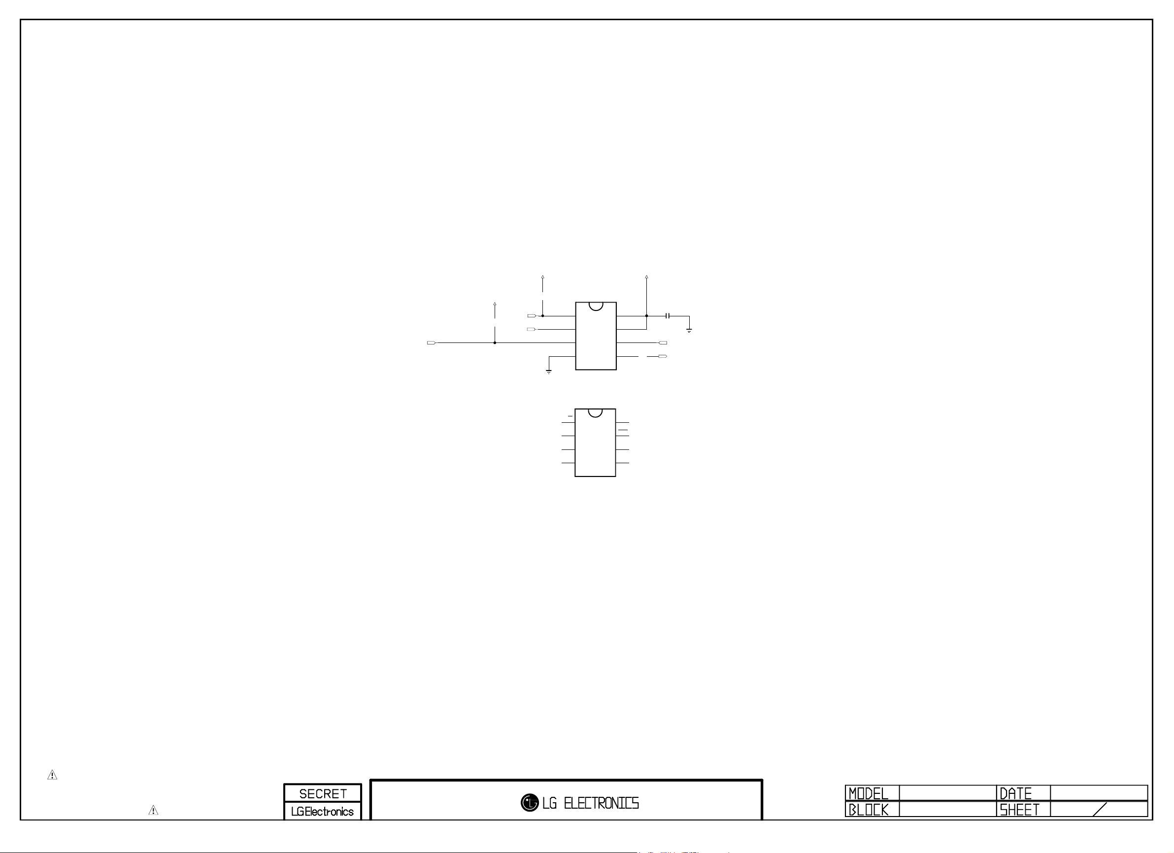
Serial Flash for SPI boot
Copyright © 2014 LG Electronics. Inc. All rights reserved.
Only for training and service purposes
LGE Internal Use Only
/FLASH_WP
OPT
R1300
10K
+3.5V_ST
/SPI_CS
SPI_SDO
OPT
R1301
4.7K
SPI_FLASH_MACRONIX
IC1300
MX25L8006EM2I-12G
CS#
1
SO/SIO1
2
WP#
3
GND
4
8
7
6
5
VCC
HOLD#
SCLK
SI/SIO0
+3.5V_ST+3.5V_ST
R1302
33
C1300
0.1uF
SPI_SCK
SPI_SDI
SPI_FLASH_WINBOND
IC1300-*1
W25Q80BVSSIG
CS
1
DO[IO1]
2
%WP[IO2]
3
GND
4
8
7
6
5
VCC
HOLD[IO3]
CLK
DI[IO0]
THE SYMBOL MARK OF THIS SCHEMETIC DIAGRAM INCORPORATES
SPECIAL FEATURES IMPORTANT FOR PROTECTION FROM X-RADIATION.
FIRE AND ELECTRICAL SHOCK HAZARDS, WHEN SERVICING IF IS
ESSENTIAL THAT ONLY MANUFACTURES SPECIFIED PARTS BE USED FOR
THE CRITICAL COMPONENTS IN THE SYMBOL MARK OF THE SCHEMETIC.
NC5_S7LR(M1A)
S_FLASH
2013/04/29
13
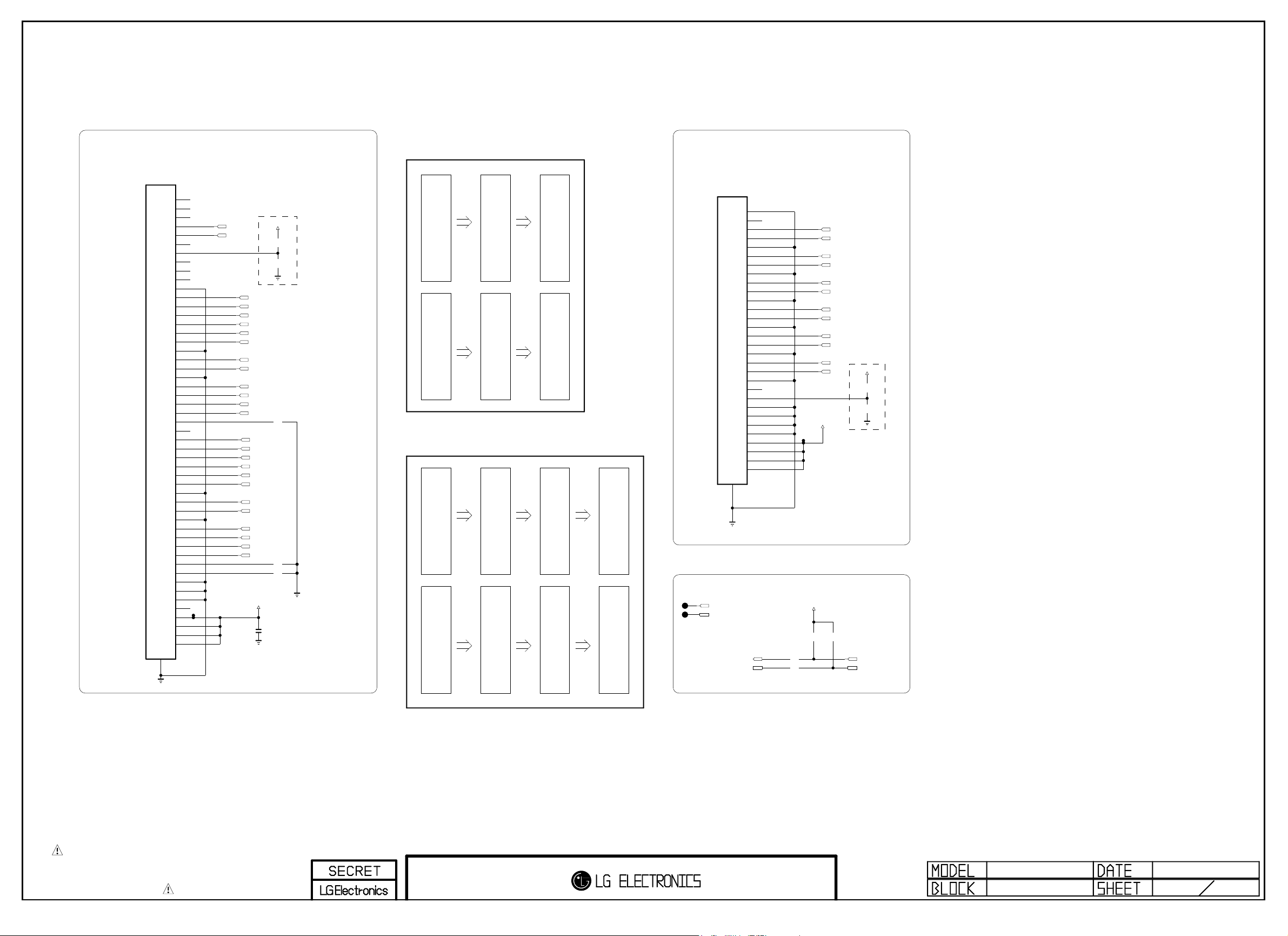
LVDS_EU
Copyright © 2014 LG Electronics. Inc. All rights reserved.
Only for training and service purposes
LGE Internal Use Only
[51Pin LVDS Connector]
(For FHD 60Hz)
MO_FHD
P1800
FI-RE51S-HF-J-R1500
1
2
3
4
5
6
7
8
9
10
11
12
13
14
15
16
17
18
19
20
21
22
23
24
25
26
27
28
29
30
31
32
33
34
35
36
37
38
39
40
41
42
43
44
45
46
47
48
49
50
51
52
VCOM_SDA
VCOM_SCL
+3.3V_Normal
RXA4+
RXA4-
RXA3+
RXA3-
RXACK+
RXACK-
RXA2+
RXA2-
RXA1+
RXA1-
RXA0+
RXA0-
R1801 0
RXB4+
RXB4-
RXB3+
RXB3-
RXBCK+
RXBCK-
RXB2+
RXB2-
RXB1+
RXB1-
RXB0+
RXB0-
R1802 0
R1803 0
PANEL_VCC
C1800
0.1uF
16V
LVDS_SEL
OPT
R1806
3.3K
OPT
R1807
10K
MO_FHD
MO_FHD
MO_FHD
FOR FHD REVERSE(10bit)
Change in S7LR
MIRROR
RXA4+
RXA4-
RXA3+
RXA3-
RXACK+
RXACK-
RXA2+
RXA2-
RXA1+
RXA1-
RXA0+
RXA0-
RXB4+
RXB4-
RXB3+
RXB3-
RXBCK+
RXBCK-
RXB2+
RXB2- RXBCK-
RXB1+
RXB1-
RXB0+
RXB0-
Pol-change
RXA0+
RXA0-
RXA1+
RXA1-
RXA2+
RXA2-
RXACK+
RXACK-
RXA3+
RXA3-
RXA4+
RXA4-
RXB0+
RXB0-
RXB1+
RXB1-
RXB2+
RXB2-
RXBCK+
RXB3+
RXB3-
RXB4+
RXB4-
FOR FHD REVERSE(8bit)
Change in S7LR
RXA4+
RXA4-
RXA3+
RXA3-
RXACK+
RXACK-
RXA2+
RXA2-
RXA1+
RXA1-
RXA0+
RXA0-
RXB4+
RXB4-
RXB3+
RXB3-
RXBCK+
RXBCK-
RXB2+
RXB2-
RXB1+
RXB1-
RXB0+
RXB0-
MIRROR
Pol-change
RXA4+
RXA4-
RXA0+
RXA0-
RXA1+
RXA1-
RXA2+
RXA2-
RXACK+
RXACK-
RXA3+
RXA3-
RXB4+
RXB4-
RXB0+
RXB0-
RXB1+
RXB1-
RXB2+
RXB2-
RXBCK+
RXBCK-
RXB3+
RXB3-
RXA0-
RXA0+
RXA1-
RXA1+
RXA2-
RXA2+
RXACK-
RXACK+
RXA3-
RXA3+
RXA4-
RXA4+
RXB0-
RXB0+
RXB1-
RXB1+
RXB2-
RXB2+
RXBCK-
RXBCK+
RXB3-
RXB3+
RXB4-
RXB4+
Shift
RXA4-
RXA4+
RXA0-
RXA0+
RXA1-
RXA1+
RXA2- RXACK-
RXA2+
RXACK-
RXACK+
RXA3-
RXA3+
RXB4-
RXB4+
RXB0-
RXB0+
RXB1-
RXB1+
RXB2-
RXB2+
RXBCK-
RXBCK+
RXB3-
RXB3+
RXA0-
RXA0+
RXA1-
RXA1+
RXA2-
RXA2+
RXACK+
RXA3-
RXA3+
RXA4-
RXA4+
RXB0-
RXB0+
RXB1-
RXB1+
RXB2-
RXB2+
RXBCK-
RXBCK+
RXB3-
RXB3+
RXB4-
RXB4+
[30Pin LVDS Connector]
(For HD 60Hz_Normal)
MO_HD
P1801
10031HR-30
1
2
3
4
5
6
7
8
9
10
11
12
13
14
15
16
17
18
19
20
21
22
23
24
25
26
27
28
29
30
31
PANEL_VCC
VCOM_SDA
VCOM_SCL
RXA3+
RXA3-
RXACK+
RXACK-
RXA2+
RXA2-
RXA1+
RXA1-
RXA0+
RXA0-
LVDS_SEL
+3.3V_Normal
OPT
R1808
3.3K
OPT
R1809
10K
EU pin assign is different from NON EU.
Because of position of HD wafer.
V-COM I2C
URSA/VCOM_SCL
URSA/VCOM_SDA
VCOM_SCL
VCOM_SDA
+3.3V_Normal
VCOM_I2C_PULL_UP
R1810
2K
VCOM_I2C
R1804
0
R1805
0
VCOM_I2C
VCOM_I2C_PULL_UP
R1811
2K
URSA/VCOM_SCL
URSA/VCOM_SDA
THE SYMBOL MARK OF THIS SCHEMETIC DIAGRAM INCORPORATES
SPECIAL FEATURES IMPORTANT FOR PROTECTION FROM X-RADIATION.
FIRE AND ELECTRICAL SHOCK HAZARDS, WHEN SERVICING IF IS
ESSENTIAL THAT ONLY MANUFACTURES SPECIFIED PARTS BE USED FOR
THE CRITICAL COMPONENTS IN THE SYMBOL MARK OF THE SCHEMETIC.
L14_M1A
LVDS_EU
2013.07.15
18
 Loading...