

Page 1

LCD TV
SERVICE MANUAL
CAUTION
BEFORE SERVICING THE CHASSIS,
READ THE SAFETY PRECAUTIONS IN THIS MANUAL.
CHASSIS : LA85Z
MODEL : 47LG50DC
47LG50DC-UA
website:http://biz.LGservice.com
Internal Use Only
Page 2

Copyright LG Electronics. Inc. All right reserved.
Only for training and service purposes
C
2008
- 2 -
LGE Internal Use Only
CONTENTS
CONTENTS ............................................................................................. 2
PRODUCT SAFETY ................................................................................. 3
SPECIFICATION....................................................................................... 6
ADJUSTMENT INSTRUCTION .............................................................. 10
TROUBLE SHOOTING .......................................................................... 17
BLOCK DIAGRAM.................................................................................. 28
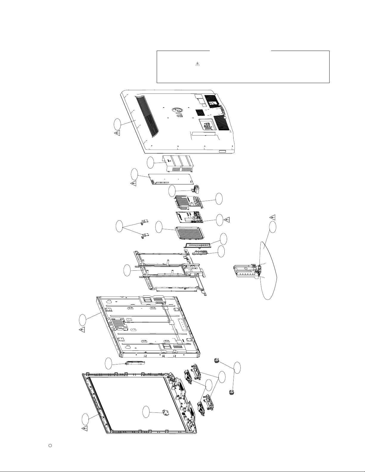
EXPLODED VIEW .................................................................................. 29
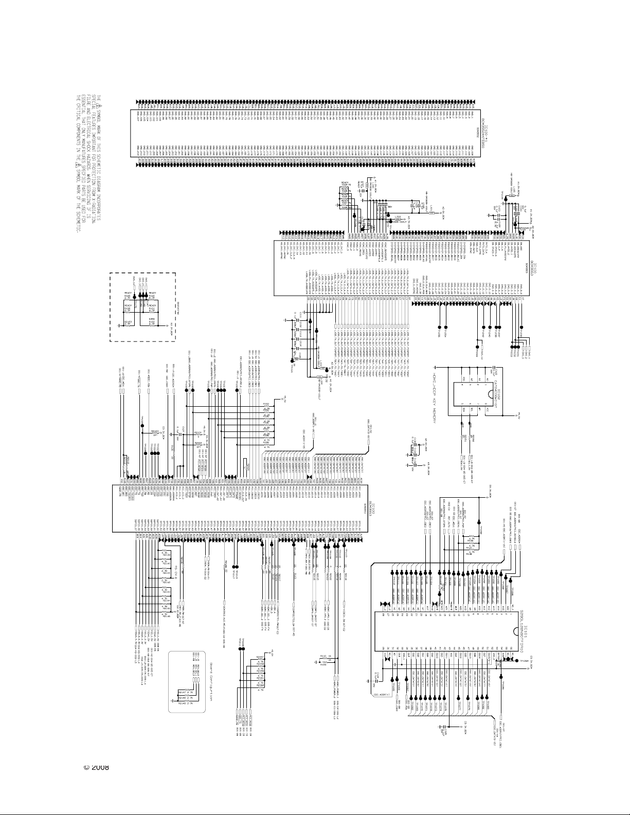
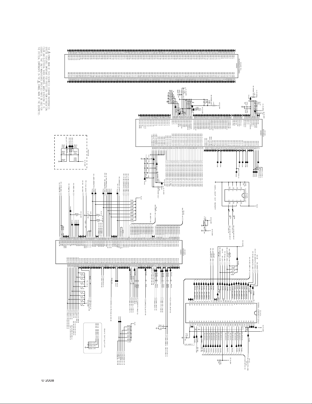
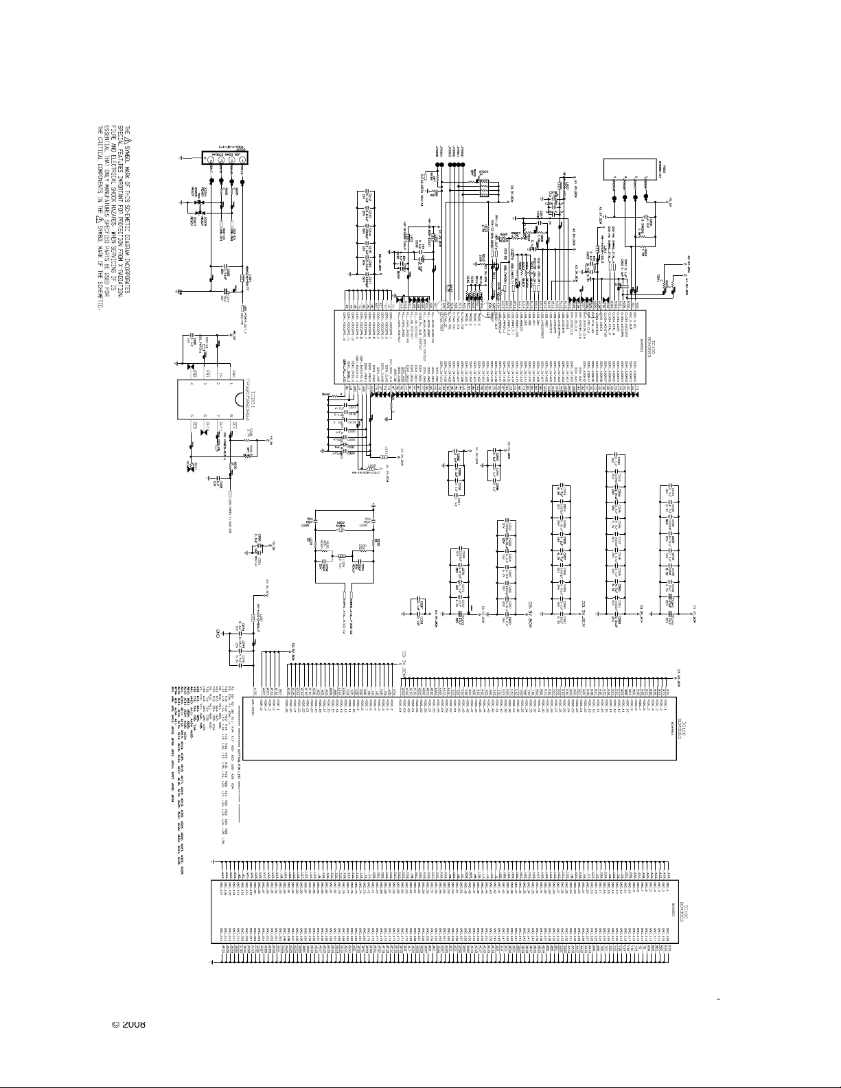
SVC. SHEET ...............................................................................................
Page 3

Copyright LG Electronics. Inc. All right reserved.
Only for training and service purposes
C
2008
- 3 -
LGE Internal Use Only
SAFETY PRECAUTIONS
Many electrical and mechanical parts in this chassis have special safety-related characteristics. These parts are identified by in the
Schematic Diagram and Exploded view.
It is essential that these special safety parts should be replaced with the same components as recommended in this manual to prevent
Shock, Fire, or other Hazards.
Do not modify the original design without permission of manufacturer.
General Guidance
An isolation Transformer should always be used during the
servicing of a receiver whose chassis is not isolated from the AC
power line. Use a transformer of adequate power rating as this
protects the technician from accidents resulting in personal injury
from electrical shocks.
It will also protect the receiver and it's components from being
damaged by accidental shorts of the circuitry that may be
inadvertently introduced during the service operation.
If any fuse (or Fusible Resistor) in this TV receiver is blown,
replace it with the specified.
When replacing a high wattage resistor (Oxide Metal Film Resistor,
over 1W), keep the resistor 10mm away from PCB.
Keep wires away from high voltage or high temperature parts.
Before returning the receiver to the customer,
always perform an AC leakage current check on the exposed
metallic parts of the cabinet, such as antennas, terminals, etc., to
be sure the set is safe to operate without damage of electrical
shock.
Leakage Current Cold Check(Antenna Cold Check)
With the instrument AC plug removed from AC source, connect an
electrical jumper across the two AC plug prongs. Place the AC
switch in the on position, connect one lead of ohm-meter to the AC
plug prongs tied together and touch other ohm-meter lead in turn to
each exposed metallic parts such as antenna terminals, phone
jacks, etc.
If the exposed metallic part has a return path to the chassis, the
measured resistance should be between 1MΩ and 5.2MΩ.
When the exposed metal has no return path to the chassis the
reading must be infinite.
An other abnormality exists that must be corrected before the
receiver is returned to the customer.
Leakage Current Hot Check (See below Figure)
Plug the AC cord directly into the AC outlet.
Do not use a line Isolation Transformer during this check.
Connect 1.5K/10watt resistor in parallel with a 0.15uF capacitor
between a known good earth ground (Water Pipe, Conduit, etc.)
and the exposed metallic parts.
Measure the AC voltage across the resistor using AC voltmeter
with 1000 ohms/volt or more sensitivity.
Reverse plug the AC cord into the AC outlet and repeat AC voltage
measurements for each exposed metallic part. Any voltage
measured must not exceed 0.75 volt RMS which is corresponds to
0.5mA.
In case any measurement is out of the limits specified, there is
possibility of shock hazard and the set must be checked and
repaired before it is returned to the customer.
Leakage Current Hot Check circuit
1.5 Kohm/10W
To Instrument's
exposed
METALLIC PARTS
Good Earth Ground
such as WATER PIPE,
CONDUIT etc.
AC Volt-meter
IMPORTANT SAFETY NOTICE
0.15uF
Page 4

Copyright LG Electronics. Inc. All right reserved.
Only for training and service purposes
C
2008
LGE Internal Use Only
- 4 -
CAUTION: Before servicing receivers covered by this service
manual and its supplements and addenda, read and follow the
SAFETY PRECAUTIONS on page 3 of this publication.
NOTE: If unforeseen circumstances create conflict between the
following servicing precautions and any of the safety precautions on
page 3 of this publication, always follow the safety precautions.
Remember: Safety First.
General Servicing Precautions
1. Always unplug the receiver AC power cord from the AC power
source before;
a. Removing or reinstalling any component, circuit board
module or any other receiver assembly.
b. Disconnecting or reconnecting any receiver electrical plug or
other electrical connection.
c. Connecting a test substitute in parallel with an electrolytic
capacitor in the receiver.
CAUTION: A wrong part substitution or incorrect polarity
installation of electrolytic capacitors may result in an
explosion hazard.
2. Test high voltage only by measuring it with an appropriate high
voltage meter or other voltage measuring device (DVM,
FETVOM, etc) equipped with a suitable high voltage probe.
Do not test high voltage by "drawing an arc".
3. Do not spray chemicals on or near this receiver or any of its
assemblies.
4. Unless specified otherwise in this service manual, clean
electrical contacts only by applying the following mixture to the
contacts with a pipe cleaner, cotton-tipped stick or comparable
non-abrasive applicator; 10% (by volume) Acetone and 90% (by
volume) isopropyl alcohol (90%-99% strength)
CAUTION: This is a flammable mixture.
Unless specified otherwise in this service manual, lubrication of
contacts in not required.
5. Do not defeat any plug/socket B+ voltage interlocks with which
receivers covered by this service manual might be equipped.
6. Do not apply AC power to this instrument and/or any of its
electrical assemblies unless all solid-state device heat sinks are
correctly installed.
7. Always connect the test receiver ground lead to the receiver
chassis ground before connecting the test receiver positive
lead.
Always remove the test receiver ground lead last.
8. Use with this receiver only the test fixtures specified in this
service manual.
CAUTION: Do not connect the test fixture ground strap to any
heat sink in this receiver.
Electrostatically Sensitive (ES) Devices
Some semiconductor (solid-state) devices can be damaged easily
by static electricity. Such components commonly are called
Electrostatically Sensitive (ES) Devices. Examples of typical ES
devices are integrated circuits and some field-effect transistors and
semiconductor "chip" components. The following techniques
should be used to help reduce the incidence of component
damage caused by static by static electricity.
1. Immediately before handling any semiconductor component or
semiconductor-equipped assembly, drain off any electrostatic
charge on your body by touching a known earth ground.
Alternatively, obtain and wear a commercially available
discharging wrist strap device, which should be removed to
prevent potential shock reasons prior to applying power to the
unit under test.
2. After removing an electrical assembly equipped with ES
devices, place the assembly on a conductive surface such as
aluminum foil, to prevent electrostatic charge buildup or
exposure of the assembly.
3. Use only a grounded-tip soldering iron to solder or unsolder ES
devices.
4. Use only an anti-static type solder removal device. Some solder
removal devices not classified as "anti-static" can generate
electrical charges sufficient to damage ES devices.
5. Do not use freon-propelled chemicals. These can generate
electrical charges sufficient to damage ES devices.
6. Do not remove a replacement ES device from its protective
package until immediately before you are ready to install it.
(Most replacement ES devices are packaged with leads
electrically shorted together by conductive foam, aluminum foil
or comparable conductive material).
7. Immediately before removing the protective material from the
leads of a replacement ES device, touch the protective material
to the chassis or circuit assembly into which the device will be
installed.
CAUTION: Be sure no power is applied to the chassis or circuit,
and observe all other safety precautions.
8. Minimize bodily motions when handling unpackaged
replacement ES devices. (Otherwise harmless motion such as
the brushing together of your clothes fabric or the lifting of your
foot from a carpeted floor can generate static electricity
sufficient to damage an ES device.)
General Soldering Guidelines
1. Use a grounded-tip, low-wattage soldering iron and appropriate
tip size and shape that will maintain tip temperature within the
range or 500
°F to 600°F.
2. Use an appropriate gauge of RMA resin-core solder composed
of 60 parts tin/40 parts lead.
3. Keep the soldering iron tip clean and well tinned.
4. Thoroughly clean the surfaces to be soldered. Use a mall wirebristle (0.5 inch, or 1.25cm) brush with a metal handle.
Do not use freon-propelled spray-on cleaners.
5. Use the following unsoldering technique
a. Allow the soldering iron tip to reach normal temperature.
(500
°F to 600°F)
b. Heat the component lead until the solder melts.
c. Quickly draw the melted solder with an anti-static, suction-
type solder removal device or with solder braid.
CAUTION: Work quickly to avoid overheating the circuit
board printed foil.
6. Use the following soldering technique.
a. Allow the soldering iron tip to reach a normal temperature
(500
°F to 600°F)
b. First, hold the soldering iron tip and solder the strand against
the component lead until the solder melts.
c. Quickly move the soldering iron tip to the junction of the
component lead and the printed circuit foil, and hold it there
only until the solder flows onto and around both the
component lead and the foil.
CAUTION: Work quickly to avoid overheating the circuit
board printed foil.
d. Closely inspect the solder area and remove any excess or
splashed solder with a small wire-bristle brush.
SERVICING PRECAUTIONS
Page 5

Copyright LG Electronics. Inc. All right reserved.
Only for training and service purposes
C
2008
- 5 -
LGE Internal Use Only
IC Remove/Replacement
Some chassis circuit boards have slotted holes (oblong) through
which the IC leads are inserted and then bent flat against the
circuit foil. When holes are the slotted type, the following technique
should be used to remove and replace the IC. When working with
boards using the familiar round hole, use the standard technique
as outlined in paragraphs 5 and 6 above.
Removal
1. Desolder and straighten each IC lead in one operation by gently
prying up on the lead with the soldering iron tip as the solder
melts.
2. Draw away the melted solder with an anti-static suction-type
solder removal device (or with solder braid) before removing the
IC.
Replacement
1. Carefully insert the replacement IC in the circuit board.
2. Carefully bend each IC lead against the circuit foil pad and
solder it.
3. Clean the soldered areas with a small wire-bristle brush.
(It is not necessary to reapply acrylic coating to the areas).
"Small-Signal" Discrete Transistor
Removal/Replacement
1. Remove the defective transistor by clipping its leads as close as
possible to the component body.
2. Bend into a "U" shape the end of each of three leads remaining
on the circuit board.
3. Bend into a "U" shape the replacement transistor leads.
4. Connect the replacement transistor leads to the corresponding
leads extending from the circuit board and crimp the "U" with
long nose pliers to insure metal to metal contact then solder
each connection.
Power Output, Transistor Device
Removal/Replacement
1. Heat and remove all solder from around the transistor leads.
2. Remove the heat sink mounting screw (if so equipped).
3. Carefully remove the transistor from the heat sink of the circuit
board.
4. Insert new transistor in the circuit board.
5. Solder each transistor lead, and clip off excess lead.
6. Replace heat sink.
Diode Removal/Replacement
1. Remove defective diode by clipping its leads as close as
possible to diode body.
2. Bend the two remaining leads perpendicular y to the circuit
board.
3. Observing diode polarity, wrap each lead of the new diode
around the corresponding lead on the circuit board.
4. Securely crimp each connection and solder it.
5. Inspect (on the circuit board copper side) the solder joints of
the two "original" leads. If they are not shiny, reheat them and if
necessary, apply additional solder.
Fuse and Conventional Resistor
Removal/Replacement
1. Clip each fuse or resistor lead at top of the circuit board hollow
stake.
2. Securely crimp the leads of replacement component around
notch at stake top.
3. Solder the connections.
CAUTION: Maintain original spacing between the replaced
component and adjacent components and the circuit board to
prevent excessive component temperatures.
Circuit Board Foil Repair
Excessive heat applied to the copper foil of any printed circuit
board will weaken the adhesive that bonds the foil to the circuit
board causing the foil to separate from or "lift-off" the board. The
following guidelines and procedures should be followed whenever
this condition is encountered.
At IC Connections
To repair a defective copper pattern at IC connections use the
following procedure to install a jumper wire on the copper pattern
side of the circuit board. (Use this technique only on IC
connections).
1. Carefully remove the damaged copper pattern with a sharp
knife. (Remove only as much copper as absolutely necessary).
2. carefully scratch away the solder resist and acrylic coating (if
used) from the end of the remaining copper pattern.
3. Bend a small "U" in one end of a small gauge jumper wire and
carefully crimp it around the IC pin. Solder the IC connection.
4. Route the jumper wire along the path of the out-away copper
pattern and let it overlap the previously scraped end of the good
copper pattern. Solder the overlapped area and clip off any
excess jumper wire.
At Other Connections
Use the following technique to repair the defective copper pattern
at connections other than IC Pins. This technique involves the
installation of a jumper wire on the component side of the circuit
board.
1. Remove the defective copper pattern with a sharp knife.
Remove at least 1/4 inch of copper, to ensure that a hazardous
condition will not exist if the jumper wire opens.
2. Trace along the copper pattern from both sides of the pattern
break and locate the nearest component that is directly
connected to the affected copper pattern.
3. Connect insulated 20-gauge jumper wire from the lead of the
nearest component on one side of the pattern break to the lead
of the nearest component on the other side.
Carefully crimp and solder the connections.
CAUTION: Be sure the insulated jumper wire is dressed so the
it does not touch components or sharp edges.
Page 6

Copyright LG Electronics. Inc. All right reserved.
Only for training and service purposes
C
2008
LGE Internal Use Only
- 6 -
4. General Specification(TV)
No. Item Specification Remark
1. Receiving System ATSC/ NTSC-M
2. Available Channel 1) VHF : 02~13
2) UHF : 14~69
3) DTV : 02-69
4) CATV : 01~135
5) CADTV : 01~135
3. Input Voltage 1) 100- 240V~, 50/60Hz Mark : 110V, 60Hz
4. Market NORTH AMERICA
5. Screen Size 47 inch Wide (1920*1080) FHD
6. Aspect Ratio 16:9
7. Tuning System FS
8. LCD Module LC470WUN-SAB1,V470H1-L03 LPL, CMO
9. Operating Environment 1) Temp : 0 ~ 40 deg
2) Humidity : ~ 80 %
10. Storage Environment 1) Temp : -20 ~ 60 deg
2) Humidity : 0 ~ 85 %
1. Application Range
This specification sheet is applied to the LCD TV used LA84Z
chassis.
2. Specification
Each part is tested as below without special appointment
1) Temperature : 25 ± 5°C (77 ± 9ºF), CST : 40 ± 5ºC
2) Relative Humidity : 65 ±10%
3) Power Voltage : Standard input voltage
(100-240V@ 50/60Hz)
* Standard Voltage of each products is marked by models
4) Specification and performance of each parts are followed
each drawing and specification by part number in
accordance with BOM.
5) The receiver must be operated for about 20 minutes prior to
the adjustment.
3. Test method
1) Performance : LGE TV test method followed.
2) Demanded other specification
- Safety : UL1492, CSA C22.2 No.1
- EMC : FCC Class B, IC Class B
SPECIFICATION
NOTE : Specifications and others are subject to change without notice for improvement
.
Page 7

Copyright LG Electronics. Inc. All right reserved.
Only for training and service purposes
C
2008
LGE Internal Use Only
- 7 -
5. Chroma & Brightness
No Item Min. Typ. Max. Unit Remark
1 White peak brightness 400 500 cd/m
2
(Center 1-point / Full White Pattern)
2 White average brightness cd/m
2
N/A
3 Brightness uniformity 80 % Full white
4 Color coordinate RED X 0.640 ± 0.03
Y 0.330 ± 0.03
GREEN X 0.280 ± 0.03
Y 0.600 ± 0.03
BLUE X 0.150 ± 0.03
Y 0.060 ± 0.03
WHITE X 0.272 ± 0.03
Y 0.277 ± 0.03
5 Color coordinate uniformity N/A
6 Contrast ratio 1000:1 1500:1
12000:1 15000:1 DCR
7 Color Temperature Cool 10,000 11,000 12,000 <Test Signal>
Standard 8,300 9,300 10,300 HDMI input
Warm 5,500 6,500 7,500 85% Full white pattern
8 Color Distortion, DG 10.0 %
9 Color Distortion, DP 10.0 deg
10 Color S/N, AM/FM 43.0 dB
11 Color Killer Sensitivity -80 dBm
6. Component Video Input (Y, CB/PB, CR/PR)
No.
Specification
Remark
Resolution H-freq(kHz) V-freq(Hz) Pixel clock
1. 720*480 15.73 60 13.5135 SDTV ,DVD 480I
2. 720*480 15.73 59.94 13.5 SDTV ,DVD 480I
3. 720*480 31.47 60 27.027 SDTV 480P
4. 720*480 31.47 59.94 27.0 SDTV 480P
5. 1280*720 45.00 60.00 74.25 HDTV 720P
6. 1280*720 44.96 59.94 74.176 HDTV 720P
7. 1920*1080 33.75 60.00 74.25 HDTV 1080I
8. 1920*1080 33.72 59.94 74.176 HDTV 1080I
9. 1920*1080 67.500 60 148.50 HDTV 1080P
10. 1920*1080 67.432 59.939 148.352 HDTV 1080P
11. 1920*1080 27.000 24.000 74.25 HDTV 1080P
12. 1920*1080 26.97 23.976 74.176 HDTV 1080P
13. 1920*1080 33.75 30.000 74.25 HDTV 1080P
14. 1920*1080 33.71 29.97 74.176 HDTV 1080P
Page 8

Copyright LG Electronics. Inc. All right reserved.
Only for training and service purposes
C
2008
LGE Internal Use Only
- 8 -
No. Specification
Remark
Resolution H-freq(kHz) V-freq(Hz) Pixel clock(MHz)
PC DDC
1 640*350 31.468 70.09 25.17 EGA X
2 720*400 31.469 70.08 28.32 DOS O
3 640*480 31.469 59.94 25.17 VESA(VGA) O
4 640*480 37.861 72.80 31.50 VESA(VGA) O
5 640*480 37.500 75.00 31.50 VESA(VGA) O
6 600*800 35.156 56.25 36.00 VESA(SVGA) O
7 800*600 37.879 60.31 40.00 VESA(SVGA) O
8 800*600 48.077 72.18 50.00 VESA(SVGA) O
9 800*600 46.875 75.00 49.50 VESA(SVGA) O
10 1024*768 48.363 60.00 65.00 VESA(XGA) O
11 1024*768 56.476 70.06 75.00 VESA(XGA) O
12 1024*768 60.023 75.02 78.75 VESA(XGA) O
13 1280*768 47.776 59.87 79.50 CVT(WXGA) O
14 1280*768 60.289 74.893 102.25 CVT(WXGA) O
15 1360*768 47.712 60.015 85.50 VESA(WXGA) O
16 1280*1024 63.981 60.020 108.00 VESA(SXGA) O
17 1280*1024 79.976 75.025 135 VESA(SXGA) O
18 1600*1200 75.00 60.00 162 VESA(UXGA) O
19 1920*1080 62.95 55.96 138.5 HDTV 1080P O
7. RGB input (PC)
Page 9

- 9 -
LGE Internal Use OnlyCopyright LG Electronics. Inc. All right reserved.
Only for training and service purposes
C
2008
8. HDMI input (PC/DTV)
No. Resolution H-freq(kHz) V-freq(Hz) Pixel clock(MHz) Remark
PC DDC
1 640*350 31.468 70.09 25.17 EGA X
2 720*400 31.469 70.08 28.32 DOS O
3 640*480 31.469 59.94 25.17 VESA(VGA) O
4 640*480 37.861 72.80 31.50 VESA(VGA) O
5 640*480 37.500 75.00 31.50 VESA(VGA) O
6 600*800 35.156 56.25 36.00 VESA(SVGA) O
7 800*600 37.879 60.31 40.00 VESA(SVGA) O
8 800*600 48.077 72.18 50.00 VESA(SVGA) O
9 800*600 46.875 75.00 49.50 VESA(SVGA) O
10 1024*768 48.363 60.00 65.00 VESA(XGA) O
11 1024*768 56.476 70.06 75.00 VESA(XGA) O
12 1024*768 60.023 75.02 78.75 VESA(XGA) O
13 1280*768 47.776 59.87 79.50 CVT(WXGA) O
14 1360*768 47.712 60.015 85.50 VESA(WXGA) O
15 1280*1024 63.981 60.020 108.00 VESA(SXGA) O
16 1280*1024 79.976 75.025 135 VESA(SXGA) O
17 1600*1200 75.00 60.00 162 VESA(UXGA) O
18 1920*1080 67.5 60 148.5 HDTV 1080P O
DTV
1 720*480 31.47 60 27.027 SDTV 480P
2 720*480 31.47 59.94 27.00 SDTV 480P
3 1280*720 45.00 60.00 74.25 HDTV 720P
4 1280*720 44.96 59.94 74.176 HDTV 720P
5 1920*1080 33.75 60.00 74.25 HDTV 1080I
6 1920*1080 33.72 59.94 74.176 HDTV 1080I
7 1920*1080 67.500 60 148.50 HDTV 1080P
8 1920*1080 67.432 59.939 148.352 HDTV 1080P
9 1920*1080 27.000 24.000 74.25 HDTV 1080P
10 1920*1080 26.97 23.976 74.176 HDTV 1080P
11 1920*1080 33.75 30.000 74.25 HDTV 1080P
12 1920*1080 33.71 29.97 74.176 HDTV 1080P
Page 10

Copyright LG Electronics. Inc. All right reserved.
Only for training and service purposes
C
2008
LGE Internal Use Only
- 10 -
ADJUSTMENT INSTRUCTION
1. Application Range
These instructions are applied to all of the LCD TV, LA84Z
Chassis.
2. Notice
2.1 Because this is not a hot chassis, it is not necessary to
use an isolation transformer. However, the use of
isolation transformer will help protect test instrument.
2.2 Adjustment must be done in the correct order. But it is
flexible when its factory local problem occurs.
2.3 The adjustment must be performed in the circumstance of
25±5°C of temperature and 65±10% of relative humidity if
there is no specific designation.
2.4 The input voltage of the receiver must keep 220V, 60Hz.
2.5 Before adjustment, execute Heat-Run for 15 minutes.
O After Receive 100% Full white pattern then process
display.
O How to make set white pattern
A. Press Power ON button of Adjust. Remocon
B. Press ADJ button of Adjust. remocon. Select "10. Test
pattern" and, after select "White" using navigation
button, and then you can see 100% Full White
pattern.
* In this status you can maintain Heat-Run useless any
pattern generator
Note) If you maintain one picture over 20 minutes (Especially
sharp distinction black with white pattern – 13Ch, or
Cross hatch pattern – 09Ch) then it can appear image
stick near black level
3. Adjust ADC(MST3361)
3.1 Overview
The ADC adjustment automatically sets the optimum black
level and the gain and compensates the RGB deviation at the
Analog-to-Digital converter
3.2 Devices and conditions to use
1) RS-232C Jig, RS-232C Cable, Phone cable
2) MSPG-925FA Serise Pattern Generator(MSPG-925FA)
- Resolution: 480i, 1080p
- Pattern name: Horizontal 100% Color Bar Pattern
- Pattern level: 0.7±0.1 Vp-p
- Image
3.3 How to adjust
3.3.1 ADC 480i Comp1
1) Check the Component1 connection condition from the
used device.
2) Apply 480i Mode, Horizontal 100% Color Bar Pattern
to Comp1 port.
(MSPG-925FA => Model: 209, Pattern: 65)
3) Set the input to Component1 and select ‘Normal’ as
video.
4) Wait for one second or longer after receiving the
signal, press the ADJ key of the R/C to enter into 'EzAdjust', select '3. ADC 480i Comp1', and press the
Enter key to automatically adjust.
5) If it is normally adjusted, the message "ADC
Component1 Success" is displayed.
6) If it is not normally adjusted, the message 'ADC
Component1 480i Fail' is displayed. If the component
is not connected, the message Component1 Not
Connected, or if the input format is not 480i, the
message 'Not Valid Format', or if there is no input
signal, the message 'Check Signal Status' is displayed
for one second.
7) If the adjustment is failed, check the pattern or the
adjustment condition and then readjust
Page 11

- 11 -
LGE Internal Use OnlyCopyright LG Electronics. Inc. All right reserved.
Only for training and service purposes
C
2008
3.3.2 ADC 1080p Comp1/RGB
1) Check the connection condition of Component1 and
RGB from the device to use.
2) Apply 1080p Mode, 100% Horizontal Color Bar Pattern
to Comp1 and RGB port.
(MSPG-925 Series => model:225 , pattern:65 )
3) Set the input to Component1 and select ‘Normal’ as
video.
4) Wait for one second or longer after receiving the signal,
press the ADJ key of the R/C to enter into 'Ez-Adjust',
select '4. ADC 1080p Comp1/RGB', and press the
Enter key to automatically adjust the component1.
5) If it is normally adjusted, the message "ADC
Component1 Success" is displayed, or if not, the
message 'ADC Component1 1080p Fail' is displayed.
6) When adjusting the Component1 is ended, it is
automatically switched to the RGB-DTV Mode and the
RGT adjustment is started. If it is normally adjusted, the
message "ADC RGB 1080P Success" is displayed.
7) If it is not normally adjusted, check the pattern or the
adjustment condition, and then readjust. The error
message is same to 6).
8) If the adjustment is ended, press the ADJ key to exit
from the adjustment mode. If the 7) adjustment is
ended, press the ADJ or the Exit of the adjustment R/C
to exit from the adjustment mode.
4. EDID(The Extended Display Identification
Data) / DDC(Display Data Channel) download
4.1 Overview
VESA specification. Function to implement the "Plug and
Play" for automatically reconfiguring the user°Øs environment
to directly use by exchanging the information with no direct
command to the PC or the monitor from the user.
4.2 Device to use
- PC (S/W included: EDID Data Write & Read)
- EDID DOWNLOAD JIG
- HDMI Cable, D-sub Cable
4.3 Adjustment wiring diagram (D/L device
configuration diagram)
4.4 How to download
1) Configure the download environment as shown at the
adjustment wiring diagram and turn on the PC.
2) Execute the DDC program. (EDID Data Write & Read)
3) Go to Model -> Open, and select the EDID data of the
desired model.
4) Check the item to download from the <Test> item
4-1) HDMI & RGB: Check Digital & Analog
4-2) (Only)HDMI: Check Digital only
5) Press ESC(Cancel Mode) -> F8(Auto Mode). (Set Auto
Detecting)
6) Connect the desired signal cable to the set.
7) Make sure that the popup "Proceed to write?" is displayed.
8) Press the Enter key or the space key to download.
9) After downloading, check the OK message and disconnect
the connected cable.
LCD TV SET
(or VSC Board)
USB
D-SUB
DVI to HDMI
Device configuration diagram for HDMI EDID Data input
Page 12

Copyright LG Electronics. Inc. All right reserved.
Only for training and service purposes
C
2008
LGE Internal Use Only
- 12 -
4.5 EDID DATA
Note) Because downloading can be down at the power on
mode only, if it is not set, press the Power ON key of
the remote controller to proceed.
O HDMI1 EDID (DDC (Display Data Channel) Data
O HDMI2 EDID (DDC (Display Data Channel) Data
O Analog (RGB) EDID table
Page 13
Copyright LG Electronics. Inc. All right reserved.
Only for training and service purposes
C
2008
LGE Internal Use Only
- 13 -
5. Adjusting the White Balance
5.1 Overview
- Purpose and principle for adjusting the white balance
- Purpose : Adjust the white balance to reduce the deviation
of the module.
- Principle: The full dynamic range of the module when the
RGB gain on the OSD is 192. In order to adjust the white
balance with no saturation of the full dynamic range and the
data, fix one of the RGB gains to 192 and decrease the
remaining two gains to adjust
5.2 Device to use
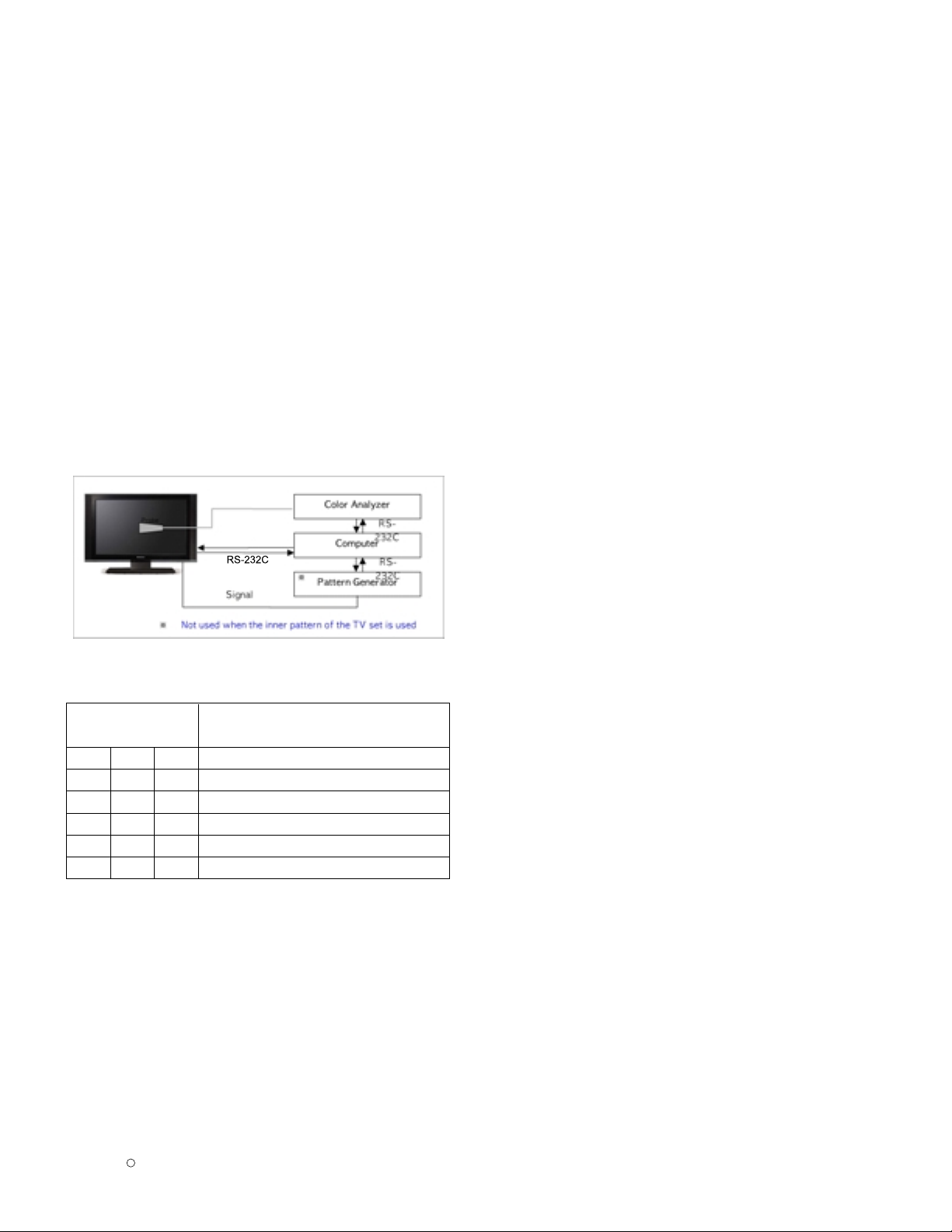
1) Color Analyzer : CA-210 (NCG: CH 9 / WCG: CH12)
2) Computer to adjust (needed for the automatic adjustment,
possible to communicate with the RS-232C)
3) Adjustment remote controller
4) Video Signal Generator MSPG-925F 720p/216Gray
(Model:217, Pattern:78)
=> Applied only when the inner pattern cannot be used
*Use the Color Analyzer with the matrix calibrated by the CS-
1000
5.3 Measuring instrument wiring diagram
5.4 RS-232C Command used for the automatic
adjustment
- "wb 00 00": Start Auto-adjustment of white balance.
- "wb 00 10": Start Gain Adjustment (Inner pattern)
- "jb 00 c0" :
- …
- "wb 00 1f": End of Adjustment
* If it needs, offset adjustment (wb 00 20-start, wb 00 2f-
end)
- "wb 00 ff": End of white balance adjustment (inner pattern
disappear)
6. How to adjust
6.1 How to adjust automatically
1) The adjustment condition should be set by the Power On
key.
2) Perform the zero calibration of the Color Analyzer and
place the probe close to the display center.
3) Connect the communication cable (RS-232C).
4) Select the desired model of the adjustment program and
perform the adjustment.
5) After the adjustment is ended (check the OK sign), check
the adjustment condition for each mode of the set.
(Warm, Medium, Cool)
6) Disconnect the probe and the communication cable to end
the adjustment.
* The adjustment should be started with "wb 00 00" and ended
with "wb 00 ff", and the offset should be adjusted when
necessary.
6.2 How to adjust manually
1) The adjustment condition should be set by the Power On
key.
2) Press the ADJ of the R/C to enter into 'EZ-ADJUST'.
3) Select '10.TEST PATTERN' with the CH +/- key and press
the Enter key for 30 minutes or longer to perform the heat
run.
4) Perform the zero calibration of the Color Analyzer and fix
the sensor with the 10cm or less distance at the center of
the LCD module surface when adjusting.
5) Press the ADJ of the R/C to select '7.White-Balance' of the
Ez-Adjust and press the right arrow key(G) to enter into
the adjustment mode.
(As soon as you press 'G', the screen is entered into the
full white inner pattern.)
6) Fix one of the R/G/B gains to 192 and decrease the
remaining two gains to adjust not to exceed 192.
7) The adjustment is done at three white balances of Cool,
Medium and Warm.
* The inner pattern is basically used, and if it is not possible, the
adjustment can be done by selecting the HDMI input. NONE,
INNER or HDMI can be selected by the bottom option at the Ez
Adjust Menu 7.White Balance menu and it is set to INNER as
default. If the adjustment cannot be done by the inner pattern,
select the HDMI to adjust.
* Adjustment environment and reference
1) Environment illuminance
Adjust it to 10 LUX or less at the place where the light
source such as lamp should be blocked at maximum.
2) Probe location
- PDP: Locate the Color Analyzer (CA-100, CA-100+,
CA210) close to the module surface to measure and
adjust
- LCD: Maintain the Color Analyzer (CA-210) close to the
module surface by 10cm or less and keep the probe
of the Color Analyzer perpendicular to the module
surface (80°~ 100°).
3) Aging time
- Keep the power on after the aging start (with no power off)
to perform the heat run for 15 minutes or longer.
- Keep the white pattern with the inner pattern for the PDP.
- For the LCD, make sure that the back light is turned on by
using no signal and the full white pattern or others.
RS-232C COMMAND
Meaning
[CMD ID DATA]
wb 00 00 White Balance adjustment start.
wb 00 10 Start of adjust gain (Inner white pattern)
wb 00 1f End of gain adjust
wb 00 20 Start of offset adjust(Inner white pattern)
wb 00 2f End of offset adjust
wb 00 ff
End of White Balance adjust(Inner pattern disappeared)
Page 14
Copyright LG Electronics. Inc. All right reserved.
Only for training and service purposes
C
2008
LGE Internal Use Only
- 14 -
6.3 Reference
(White Balance adjustment coordinate and
White balance)
O Brightness: Full white 216 Gray
O Standard color coordinate and white balance when using the
CS-1000
O Standard color coordinate and white balance when using the
CA-210 (CH 9)
7. Select the option by country
7.1 Overview
- The option selection is applied to the North American model
only, which selects the rating related country.
- Applied models: LA84A Chassis applied None USA
Model(Canada, Mexico)
7.2 How to select
1) Press the In-Start key of the R/C and press the red oval
OP1(PIP CH-) key to enter into the Factory Option menu.
2) Select 1.USA, 2.CANADA or 3.MEXICO from the country
select according to the destination. At this time, use the
volume +/- key to adjust
8. Set the shipping mode (In-stop)
- After completing the final test, in order to set the set to the
shipping condition, press the In-Stop key of the R/C to make
sure that the set is turned off.
9. GND and resisting pressure test
9.1 How to test
1) Preparing for the automatic test on the GND & resisting
pressure
- Make sure that the power cord is completely inserted into
the set. (When it is disconnected or loosened, test after
inserting it)
2) Perform the automatic test on the GND & resisting
pressure
- The set with power cord, the cord and the A/V completely
inserted into the tuner is loaded on the pallet and entered
into the automatic test process.
- Connect the D-terminal AV JACK tester
- Turn on the automatic (GWS103-4)
- Perform the GND TEST
- If it is not good, the buzzer is operated to notify the test
result to the operator.
- If it is OK, it is automatically switched to the resisting
pressure test. (Disconnect the cord and the A/V from the
AV JACK BOX)
- Perform the resisting pressure test
- If it is not good, the buzzer is operated to notify the test
result to the operator.
- If it is OK, the GOOD LAMP is turned and the stopper is
moves down, and it moves to the next process.
9.2 Items to manage
O TEST voltage
- GND:1.5KV/min at 100mA
- SIGNAL:3KV/min at 100mA
O TEST time:1 second
O TEST POINT
- GND TEST = between POWER CORD GND and
SIGNAL CABLE METAL GND
- Resisting pressure TEST = between POWER CORD
GND and LIVE & NEUTRAL
O LEAKAGE CURRENT: Set to 0.5mArms
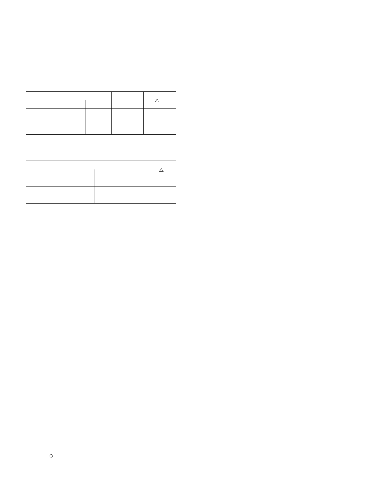
Color temperature
Color Coordination
Temp
UV
xy
COOL 0.276 0.283 11000K 0.0000
MEDIUM 0.285 0.293 9300K 0.0000
WARM 0.313 0.324 6500K 0.0000
Color temperature
Color Coordination
Temp
UV
xy
COOL 0.276±0.002 0.283±0.002 11000K 0.0000
MEDIUM 0.285±0.002 0.293±0.002 9300K 0.0000
WARM 0.313±0.002 0.324±0.002 6500K 0.0000
Page 15
- 15 -
LGE Internal Use OnlyCopyright LG Electronics. Inc. All right reserved.
Only for training and service purposes
C
2008
10. ISP Download (option)
10.1 Overview
The Micom upgrade via the external port for the service for
the customer.
10.2 Device to use
1) PC
2) B/D for the interface (IIC & ISP)
3) Jig for downloading (for the power supply)
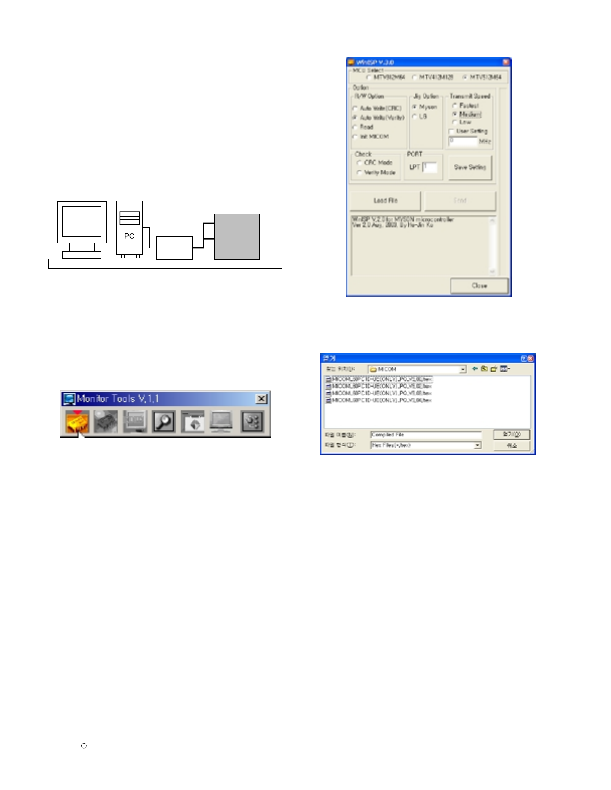
10.3 Adjustment wiring diagram (Download device
configuration diagram)
10.4 Adjustment condition (Download condition)
- IC name & Circuit number: MYSON MTV416GMF & IC4015
- Power supply: 5V (P4004 Pin 3)
- SCL: D-sub Pin 10
- SDA: D-sub Pin 7
10.5 How to adjust (for downloading)
1) fter executing LGE Monitor Tools v1.1, click the first icon.
(See the figure)
2) When the screen is displayed as shown at the below
figure, set the items as follows:
- MCU Select: MTV512M64
- R/W Option: Auto Write(Verify)
- Jig Option: Myson
- Transmit Speed: Medium
- Check: blank
- PORT: Select the Parallel Port to use (LPT1 in general)
*caution: Select the EPP as LPT from the ROM BIAS setting.
3) Click the Load File Button, and select the desired Hex File
to download.
(If no file is displayed, make sure that the file format is
selected as Hex file (*.hex))
4) Click 'Send Button'
Main B/D
Interface B/D
Page 16
11. USB S/W Download (option)
11-1. Overview
The USB download is for the quick service response via the
S/W upgrade and for applying the S/W upgrade necessary for
the board adjustment
11-2. How to download
1) After turning on the set, make sure that the display screen
is turned on.
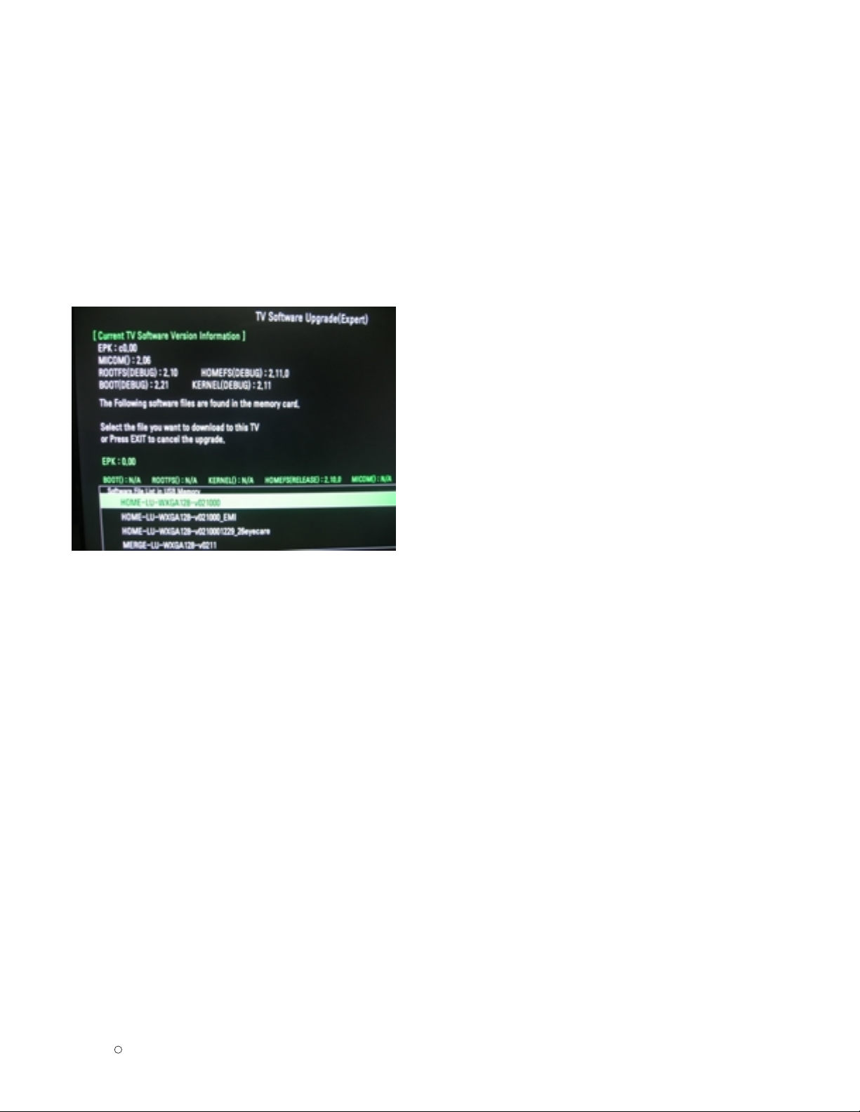
2) When the USB Memory Stick with the upgrade file applied
is inserted into the USB jack on the main board, the
following screen (example) is displayed after several
seconds
3) Check the current version at [Current TV Software Version
Information], check the S/W version to upgrade at
[Software file list in USB Memory], and press the Enter
button of the TV remote controller.
4) Downloading is proceeded as shown at the below screen,
and when it is ended, turning on/off is automatically done.
(When the automatic proceeding is not smoothly done,
manually perform the power On/Off).
5) When downloading is ended, remove the USB Memory
Stick from the USB jack.
6) Press the IN-START button of the remote controller to
check the upgraded S/W version.
- 16 -
LGE Internal Use OnlyCopyright LG Electronics. Inc. All right reserved.
Only for training and service purposes
C
2008
Page 17
Copyright LG Electronics. Inc. All right reserved.
Only for training and service purposes
C
2008
LGE Internal Use Only
- 17 -
TROUBLESHOOTING
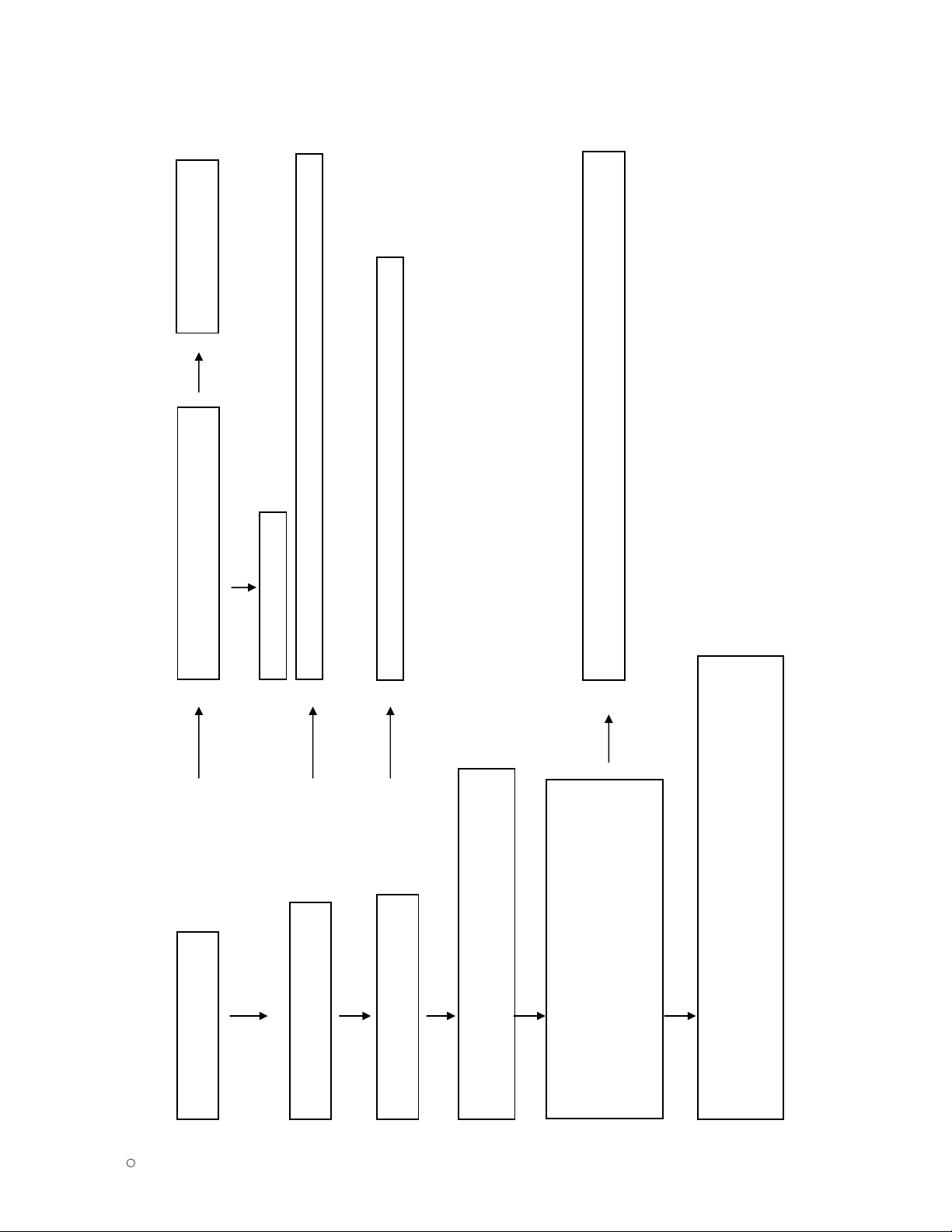
1. TV/CATV-VIDEO
Check TU1 Pin16(Video output)
Can you see the normal signal?
Check the input(Pin1) of LPF(IC808).
Can you see the normal waveform?
YES
NO
Could you measure voltage of TU1 & IIC lines?
Are they all normal?
Check the output(Pin8) of LPF(IC808).
Can you see the normal waveform?
Check the input(PinAN16) of BCM3553(IC100).
Measure waveform at C658 because itís more easy to check.
Can you see the normal waveform?
NO
You should check power line
& IIC lines.
YES
You should replace TUNER.
NO
After checking video signal line & the Power of LPF you should decide to replace item or not.
NO
After checking the Power of LPF you should decide to replace LPF or not.
NO
This board has big problem because Main chip(BCM3553) have some troubles.
After checking thoroughly all path once again, You should decide to replace BCM3553 or not.
YES
YES
Check all power domain of FRC-9459M (IC1000)
(3.3V, 1.3V_CORE,1.3V_PLL,3.3V,1.8V,2.5V)
& crystal output (X1000 / 20.25MHz)&FRC_RESET
Measure Power & waveform at L1008,L1007,L1002,L1013,
L1014,L1015~L1018&C1006&R1029
because itís more easy to check.
Can you see the normal waveform?
YES
This board has big problem because FRC chip(FRC-9459M) have some troubles.
After checking thoroughly all path once again, You should decide to replace
FRC-9459M.
Although you replace it, you cannot see normal display, decide to replace
Main chip(BCM3553)
YES
Page 18
Copyright LG Electronics. Inc. All right reserved.
Only for training and service purposes
C
2008
- 18 -
LGE Internal Use Only
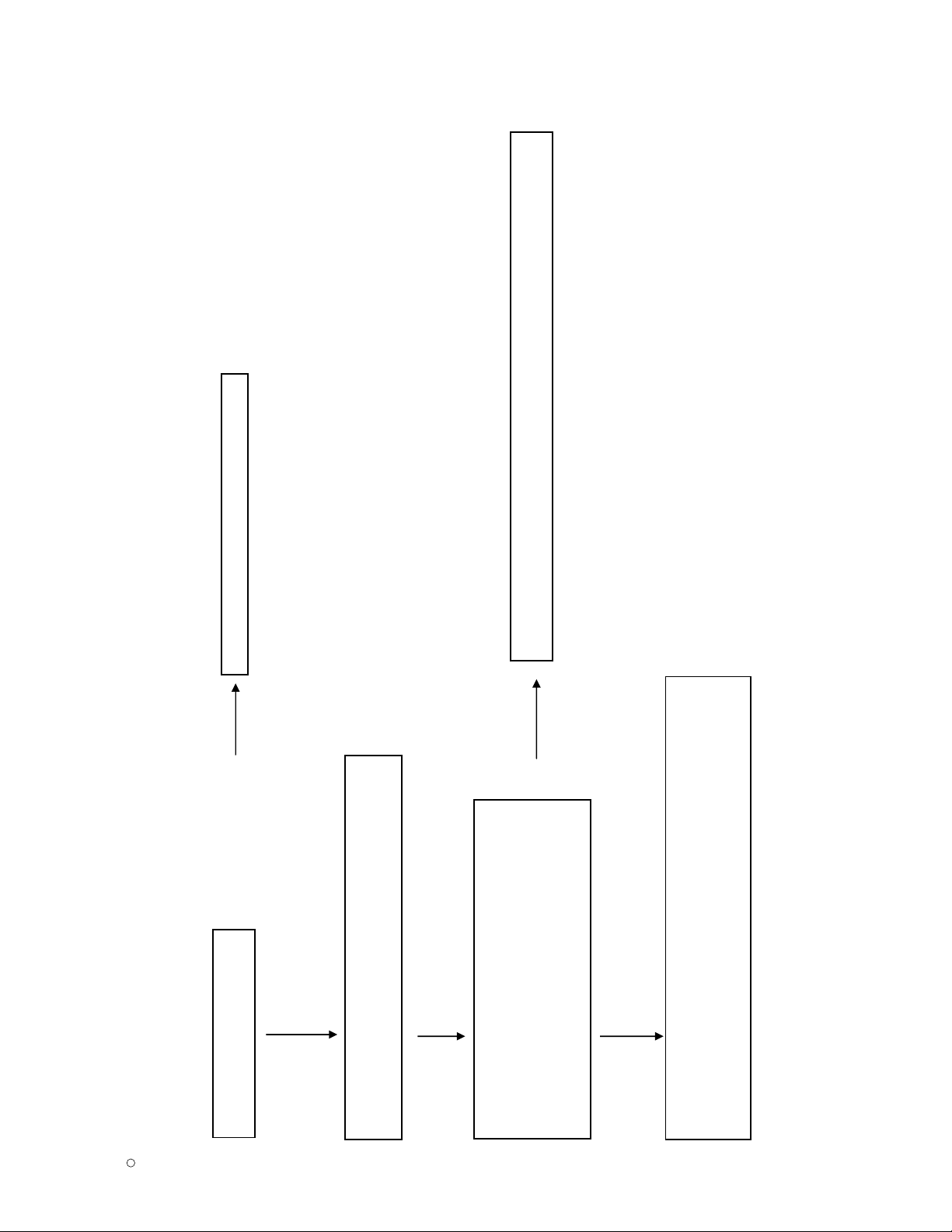
2. AV-VIDEO
Check JK701, JK707
Can you see the normal waveform?
NO
JK701,JK707 may have problem. Replace this Jack.
Check the input (Pin AN17,AM19) of BCM3553(IC100).
Measure waveform at C651,C652 because itís more easy to check.
Can you see the normal waveform?
YES
NO
This board has big problem because Main chip(BCM3553) have some troubles.
After checking thoroughly all path once again, You should decide to replace BCM3553 or not.
Check all power domain of FRC-9459M (IC1000)
(3.3V, 1.3V_CORE,1.3V_PLL,3.3V,1.8V,2.5V)
& crystal output (X1000 / 20.25MHz)&FRC_RESET
Measure Power & waveform at L1008,L1007,L1002,L1013,
L1014,L1015~L1018&C1006&R1029
because itís more easy to check.
Can you see the normal waveform?
YES
This board has big problem because FRC chip(FRC-9459M) have some troubles.
After checking thoroughly all path once again, You should decide to replace
FRC-9459M.
Although you replace it, you cannot see normal display, decide to replace
Main chip(BCM3553)
YES
Page 19
Copyright LG Electronics. Inc. All right reserved.
Only for training and service purposes
C
2008
- 19 -
LGE Internal Use Only
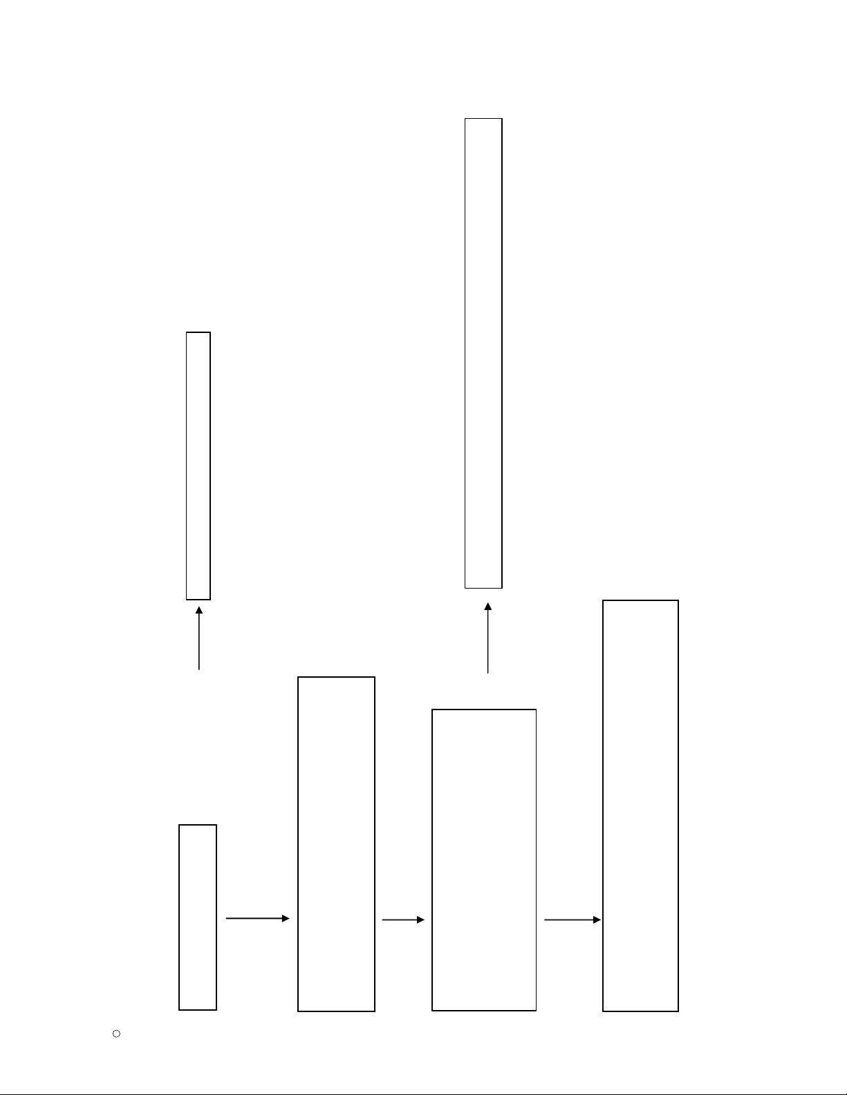
3. COMPONENT-VIDEO
Check JK700,JK702.
Can you see the normal waveform?
JK700,JK702 may have problem. Replace this Jack.
Check the input (Pin AL21,AM21,AN21 and PinAN22,AL22,AP22)
of BCM3553(IC100).
Measure waveform at C638,C639,C640 and C628,C629,C630
because itís more easy to check.
Can you see the normal waveform?
YES
NO
NO
This board has big problem because Main chip(BCM3553) have some troubles.
After checking thoroughly all path once again, You should decide to replace BCM3553 or not.
Check all power domain of FRC-9459M (IC1000)
(3.3V, 1.3V_CORE,1.3V_PLL,3.3V,1.8V,2.5V)
& crystal output (X1000 / 20.25MHz)&FRC_RESET
Measure Power & waveform at L1008,L1007,L1002,L1013,
L1014,L1015~L1018&C1006&R1029
because itís more easy to check.
Can you see the normal waveform?
YES
This board has big problem because FRC chip(FRC-9459M) have some troubles.
After checking thoroughly all path once again, You should decide to replace
FRC-9459M.
Although you replace it, you cannot see normal display, decide to replace
Main chip(BCM3553)
YES
Page 20
Copyright LG Electronics. Inc. All right reserved.
Only for training and service purposes
C
2008
- 20 -
LGE Internal Use Only
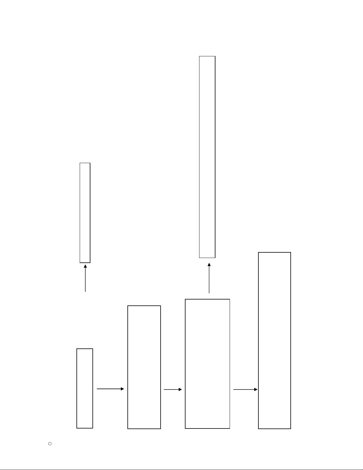
4. RGB-VIDEO
Check JK705.
Can you see the normal waveform?
YES
JK705 may have problem. Replace this Jack.
NO
Check the input (Pin AK16,AN15,AM15,AH16,AJ16)
of BCM355x(IC100).
Measure waveform at C635,C636,C637 and R755,R758
because itís more easy to check.
Can you see the normal waveform?
NO
This board has big problem because Main chip(BCM3553) have some troubles.
After checking thoroughly all path once again, You should decide to replace BCM3553 or not.
Check all power domain of FRC-9459M (IC1000)
(3.3V, 1.3V_CORE,1.3V_PLL,3.3V,1.8V,2.5V)
& crystal output (X1000 / 20.25MHz)&FRC_RESET
Measure Power & waveform at L1008,L1007,L1002,L1013,
L1014,L1015~L1018&C1006&R1029
because itís more easy to check.
Can you see the normal waveform?
YES
This board has big problem because FRC chip(FRC-9459M) have some troubles.
After checking thoroughly all path once again, You should decide to replace
FRC-9459M.
Although you replace it, you cannot see normal display, decide to replace
Main chip(BCM3553)
YES
Page 21
Copyright LG Electronics. Inc. All right reserved.
Only for training and service purposes
C
2008
- 21 -
LGE Internal Use Only
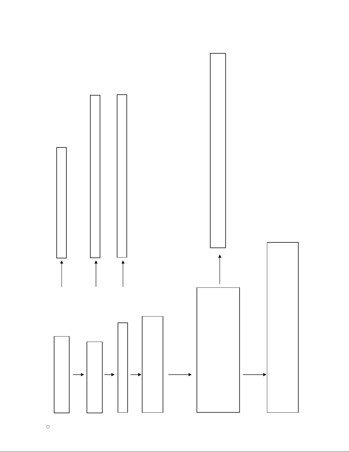
5. HDMI-VIDEO
Check input connect JK600,JK601
Can you see the normal waveform?
Check DDC communication lines
(IC601, IC602)
JK600,JK601 may have problem. Replace this Jack.
Check the output of PI3HDMI341ATR(IC600)
_HDMI1,2
Can you see the normal waveform?
After checking the Power of this chip, you should decide to replace this or not.
Check HDCP communication lines(IC102)
After checking the Power of this chip, you should decide to replace this or not.
YES
YES
YES
NO
NO
NO
NO
This board has big problem because Main chip(BCM3553) have some troubles.
After checking thoroughly all path once again, You should decide to replace BCM3553 or not.
Check all power domain of FRC-9459M (IC1000)
(3.3V, 1.3V_CORE,1.3V_PLL,3.3V,1.8V,2.5V)
& crystal output (X1000 / 20.25MHz)&FRC_RESET
Measure Power & waveform at L1008,L1007,L1002,L1013,
L1014,L1015~L1018&C1006&R1029
because itís more easy to check.
Can you see the normal waveform?
YES
This board has big problem because FRC chip(FRC-9459M) have some troubles.
After checking thoroughly all path once again, You should decide to replace
FRC-9459M.
Although you replace it, you cannot see normal display, decide to replace
Main chip(BCM3553)
YES
Page 22
Copyright LG Electronics. Inc. All right reserved.
Only for training and service purposes
C
2008
- 22 -
LGE Internal Use Only
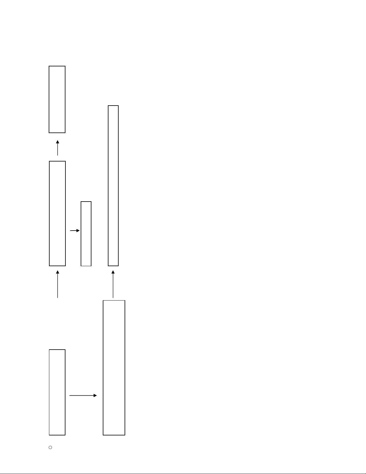
6. TV/CATV-AUDIO(IN)
Check TU1 Pin14(SIF)
Can you see the normal signal?
Check the input (Pin AN23) of BCM3553((IC100).
Measure waveform at C665 because itís more easy to check.
Can you see the normal waveform?
YES
NO
Could you measure voltage of TU1 & IIC lines?
Are they all normal?
NO
You should check power line
& IIC lines.
YES
You should replace TUNER.
NO
After checking audio signal line, you should decide to replace item or not.
Page 23
- 23 -
LGE Internal Use OnlyCopyright LG Electronics. Inc. All right reserved.
Only for training and service purposes
C
2008
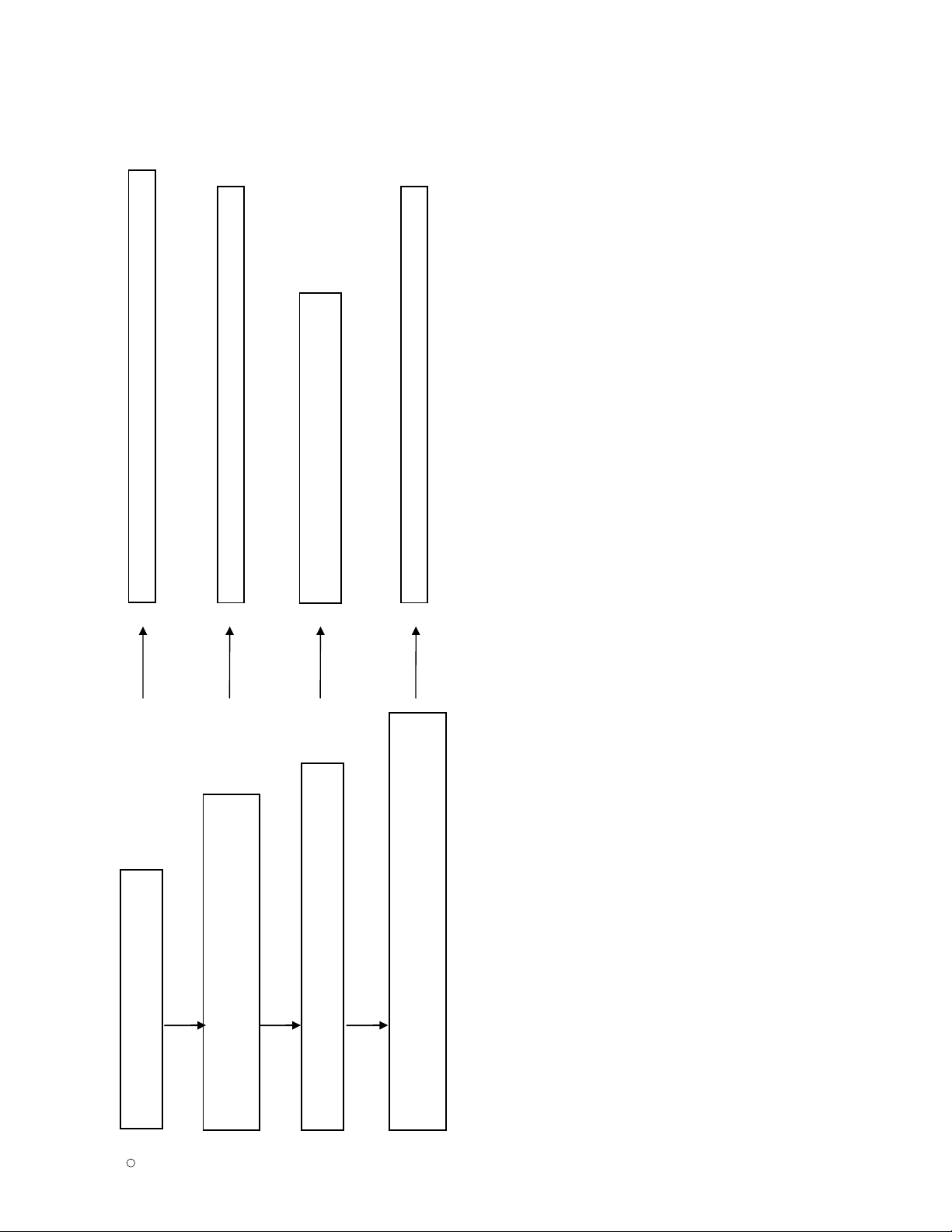
7. AV/COMPONENT/RGB_PC-AUDIO(IN)
Check JK705, JK701, JK700, JK702, JK704.
Can you see the normal waveform?
NO
JK701, JK705, JK700, JK702, JK703 may have problem. Replace this Jack.
Check the input (Pin AIN6A, AIN6B,AIN1A,AIN1B,
AIN3A,AIN3B,AIN4A,AIN4B,AIN2A,AIN2B
) of CS5345(IC500).
Can you see the normal waveform?
NO
YES
After checking audio signal line, you should decide to replace item or not.
YES
Check the Output (Pin SDOUT,SCLK,LRCK) of CS5345(IC500).
Can you see the normal waveform?
NO
After checking the Power & MLCK & reset of this chip,
you should decide to replace this or not.
YES
Check the input (Pin AH24,AJ24,AK24) of BCM3553((IC100).
Measure waveform at R554,R561,R555 because itís more easy to check.
Can you see the normal waveform?
NO
After checking audio signal line, you should decide to replace item or not.
Page 24
- 24 -
LGE Internal Use OnlyCopyright LG Electronics. Inc. All right reserved.
Only for training and service purposes
C
2008
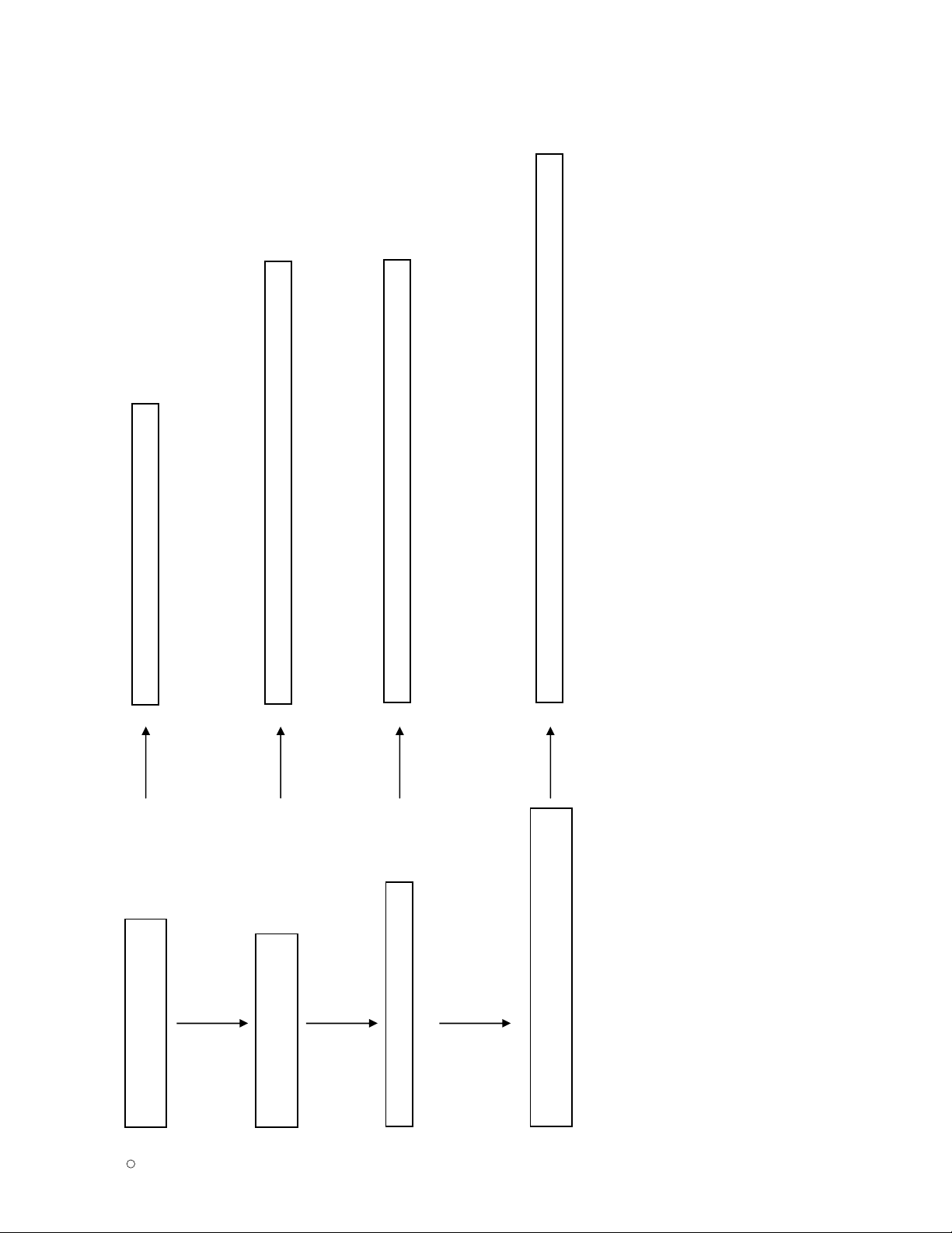
8. HDMI-AUDIO(IN)
Check input connect JK600,JK601
Can you see the normal waveform?
Check DDC communication lines
(IC601, IC602)
JK600,JK601 may have problem. Replace this Jack.
Check the output of PI3HDMI341ATR(IC600)_HDMI1/2
Can you see the normal waveform?
After checking the Power of this chip, you should decide to replace this or not.
Check HDCP communication lines(IC102)
After checking the Power of this chip, you should decide to replace this or not.
YES
YES
YES
NO
NO
NO
NO
After checking the Power & Select Pin & Etc of this chip, you should decide to replace this or not.
Page 25
- 25 -
LGE Internal Use OnlyCopyright LG Electronics. Inc. All right reserved.
Only for training and service purposes
C
2008
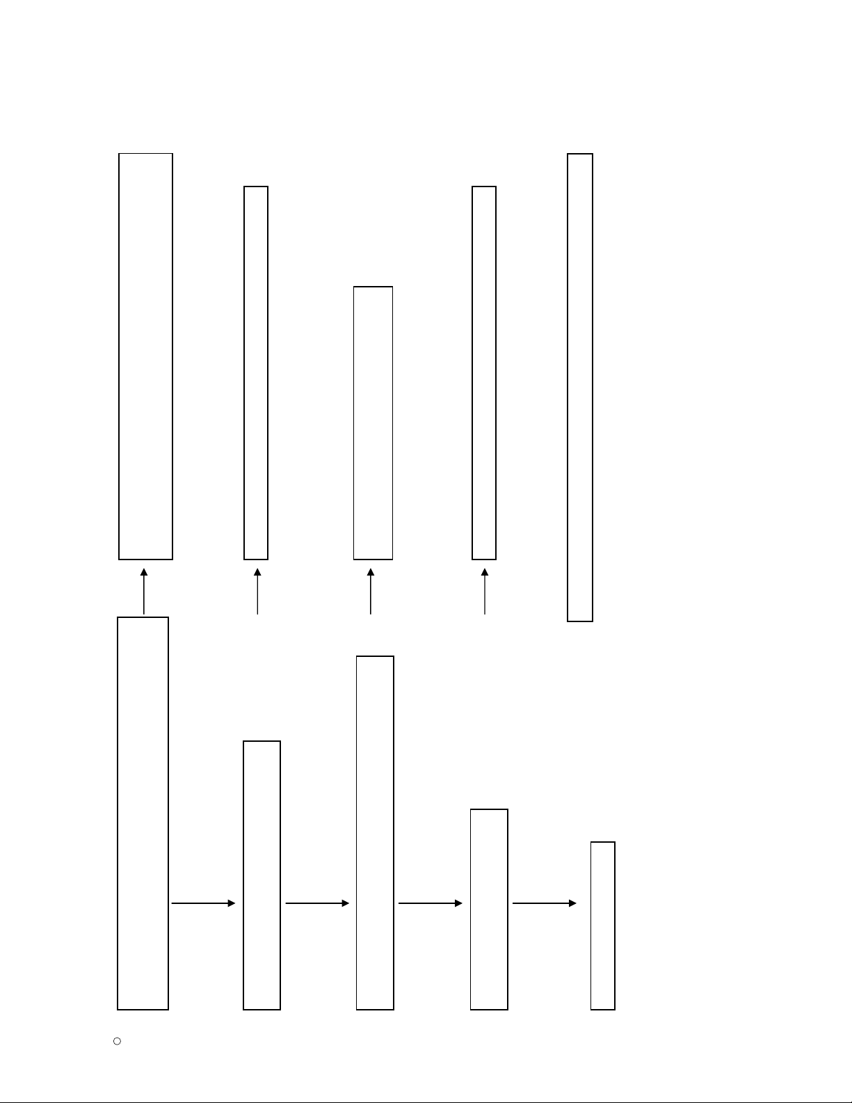
9. SPEAKER-AUDIO(OUT)
Check the output (Pin AK25,AL25,AJ25) of BCM3553(IC100).
Measure waveform at R2635,R2636,R2637 because itís more easy to check.
Can you see the normal signal?
Check the input (Pin 17,18,19) of NTP3000((IC501).
Can you see the normal waveform?
YES
NO
NO
This board has big problem because Main chip(BCM3553) have some troubles.
After checking thoroughly all path once again,
You should decide to replace BCM3553 or not.
After checking audio signal line, you should decide to replace item or not.
YES
Check the output (Pin 30,31,36,37,47,48,53,54) of NTP3000((IC501).
Can you see the normal waveform?
NO
YES
After checking the Power & I2C & Reset of this chip,
you should decide to replace this or not.
Check the speaker output wafer P501.
Can you see the normal waveform?
NO
YES
After checking audio signal line, you should decide to replace item or not.
Check the connector & Speaker
* If condition of starting sound is abnomal, you have to check IC1000(TPA3005).
Page 26
- 26 -
LGE Internal Use OnlyCopyright LG Electronics. Inc. All right reserved.
Only for training and service purposes
C
2008
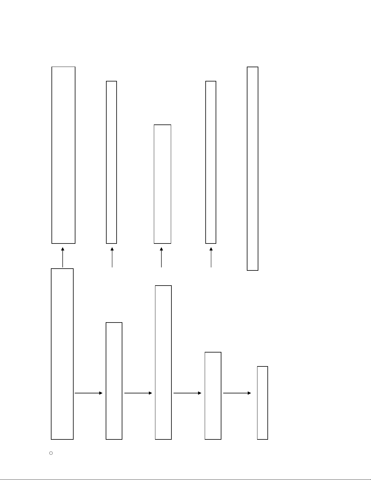
10. SPDIF & COAXIAL-AUDIO(OUT)
Check the output (Pin AK25,AL25,AJ25) of BCM3553(IC100).
Measure waveform at R2635,R2636,R2637 because itís more easy to check.
Can you see the normal signal?
Check the input (Pin 17,18,19) of NTP3000((IC501).
Can you see the normal waveform?
YES
NO
NO
This board has big problem because Main chip(BCM3553) have some troubles.
After checking thoroughly all path once again,
You should decide to replace BCM3553 or not.
After checking audio signal line, you should decide to replace item or not.
YES
Check the output (Pin 30,31,36,37,47,48,53,54) of NTP3000((IC501).
Can you see the normal waveform?
NO
YES
After checking the Power & I2C & Reset of this chip,
you should decide to replace this or not.
Check the speaker output wafer P501.
Can you see the normal waveform?
NO
YES
After checking audio signal line, you should decide to replace item or not.
Check the connector & Speaker
* If condition of starting sound is abnomal, you have to check IC1000(TPA3005).
Page 27
- 27 -
LGE Internal Use OnlyCopyright LG Electronics. Inc. All right reserved.
Only for training and service purposes
C
2008
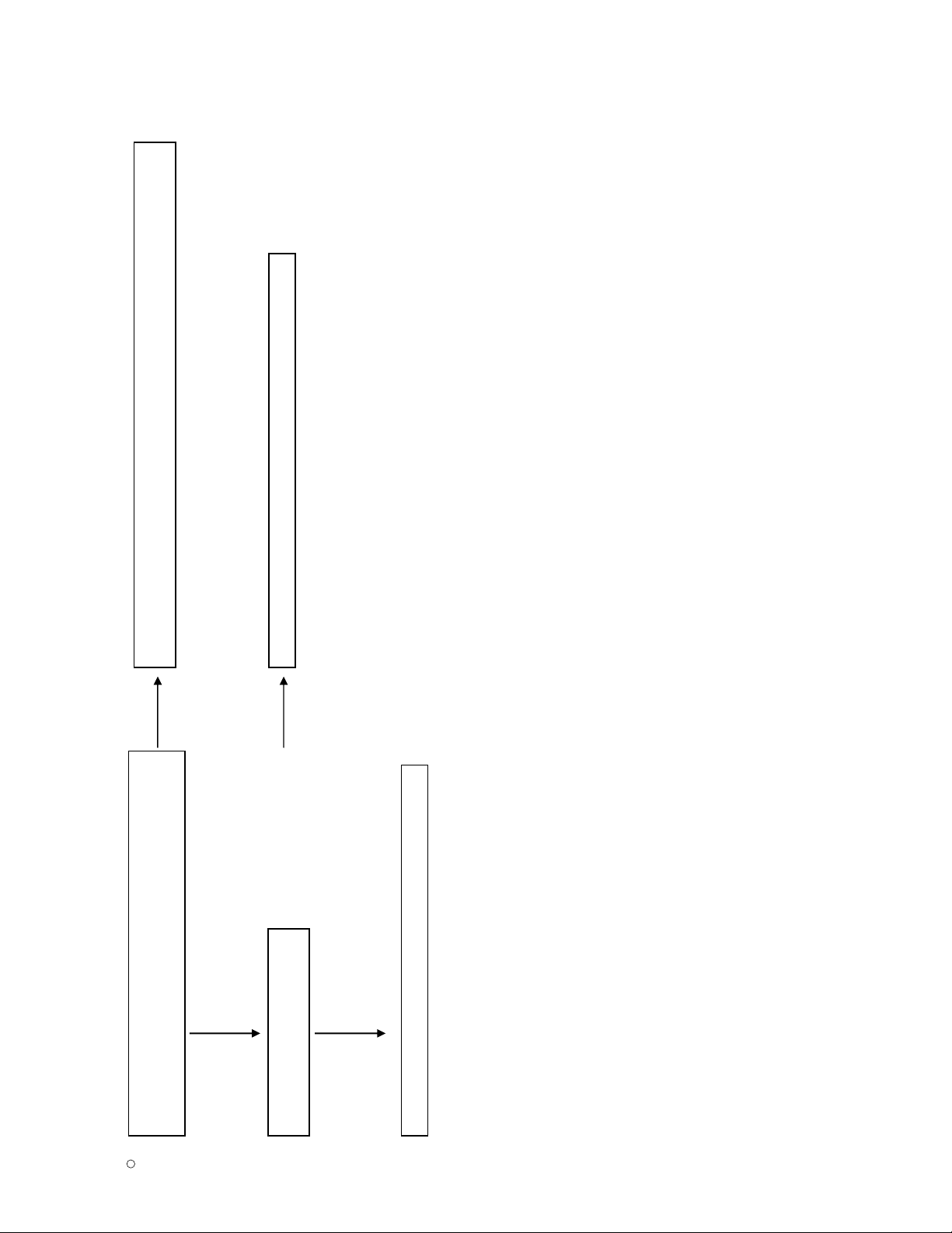
11. MNT OUT-AUDIO(OUT)
Check the output (Pin AN28, AP29) of BCM3553(IC100).
Measure waveform at R685, R686 because itís more easy to check.
Can you see the normal signal?
NO
This board has big problem because Main chip(BCM3553) have some troubles.
After checking thoroughly all path once again, You should decide to replace BCM3553 or not.
Check the input of JK705.
Can you see the normal waveform?
YES
NO
After checking audio signal line, you should decide to replace item or not.
YES
After checking the Jack, you should decide to replace item or not.
Page 28
Copyright LG Electronics. Inc. All right reserved.
Only for training and service purposes
C
2008
LGE Internal Use Only
- 28 -
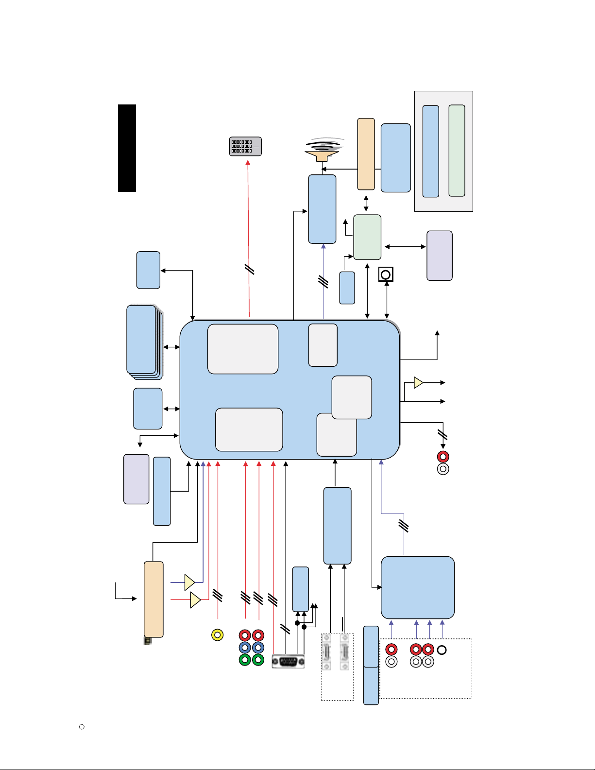
BLOCK DIAGRAM
Flash
(16MB)
DDR(32MB)
(4x16x4)
DDR(32MB)
(4x16x4)
74LVC14APW
CS5345
(Audio S/W
&A/D&)
MTV416
(Micom)
NTP3000
(D-AMP)
X200
X-tal(54 )
PI3HDMI341ATR
(2x1,S/W)
EEPROM
AT/NT Tuner
64Bit I/F
Reset
CVBS
CVBS/Y/C
Y/Cb/Cr
R/G/B
H/V Sync
Audio L/R
I2S
MNT out
(L/R)
SPDIF
OUT
I2S
Full HD(1080P)
RS-232C
Dead IC when Standby
Alive IC when Standby
Video
Front
End
Dual
HDMI
Rx0
HD/SD
Video
Encoder
Audio
DSP
BCM3552(HD)
BCM3553(FHD)
MCLK
MCLK
HDMI CEC
HDMI CEC(To Micom)
To Micom
SDA
SCL
SIF
IF(AT)
Buffer
Digital out
Buffer
Buffer
24C16
AGC CTL (From BCM)
USB2.0
I2S Audio Input
VSB/QAM/NTSC/SIF
AV1
COMP1
COMP2
DDR(32MB)
(4x16x4)
DDR(32MB)
(4x16x4)
DDR(32MB)
(4x16x4)
DDR(32MB)
(4x16x4)
DDR(32MB)
(4x16x4)
DDR(32MB)
(4x16x4)
DDR (128MB)
RGB
Y/Cb/Cr
HDMI1
HDMI2
AV1
COMP1
COMP2
RGB
Coaxial
OUT (LG50)
USB
LG50: FHD-60Hz
X400
X-tal(24 )
NVRAM
24C512
EEPROM EEPROM
LVDS
Connector(26P)
Dual
HDMI
Rx1
TPA3005D2
PHPRG4
IR & Local KEY
Page 29
Copyright LG Electronics. Inc. All right reserved.
Only for training and service purposes
C
2008
LGE Internal Use Only
- 29 -
EXPLODED VIEW
300
121
122
120
500
510
200
840
400
530
810
550
540
521
520
900
800
830
820
Many electrical and mechanical parts in this chassis have special safety-related characteristics. These
parts are identified by in the Schematic Diagram and EXPLODED VIEW.
It is essential that these special safety parts should be replaced with the same components as
recommended in this manual to prevent X-RADIATION, Shock, Fire, or other Hazards.
Do not modify the original design without permission of manufacturer.
IMPORTANT SAFETY NOTICE
Page 30
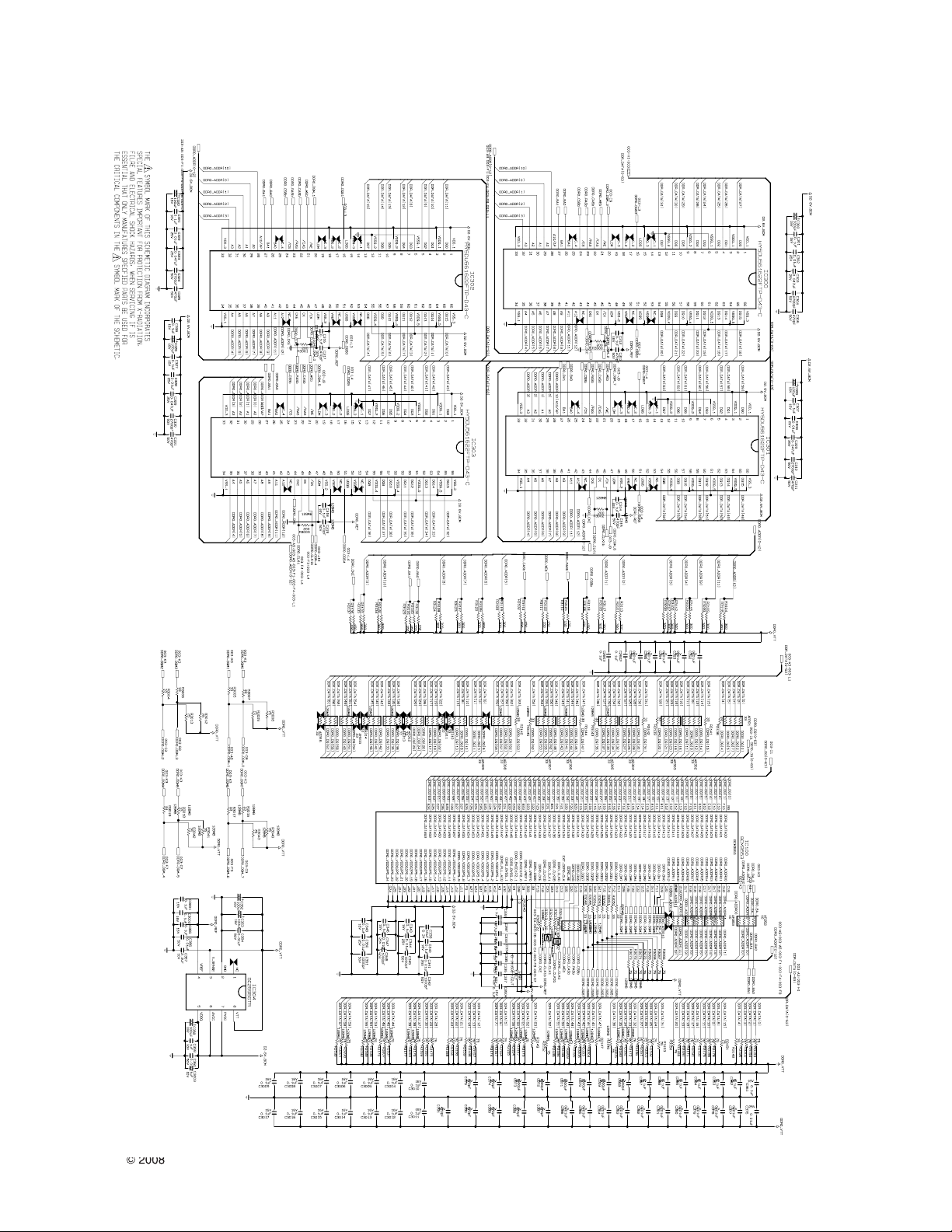
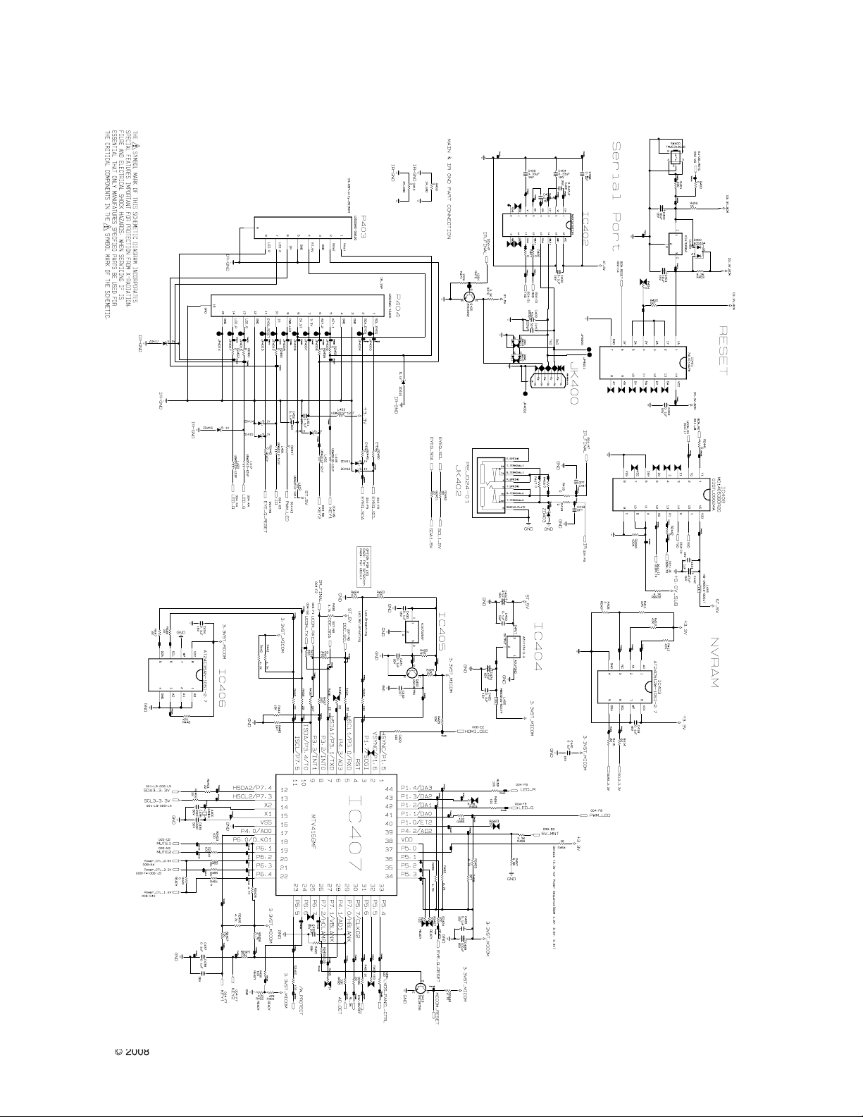
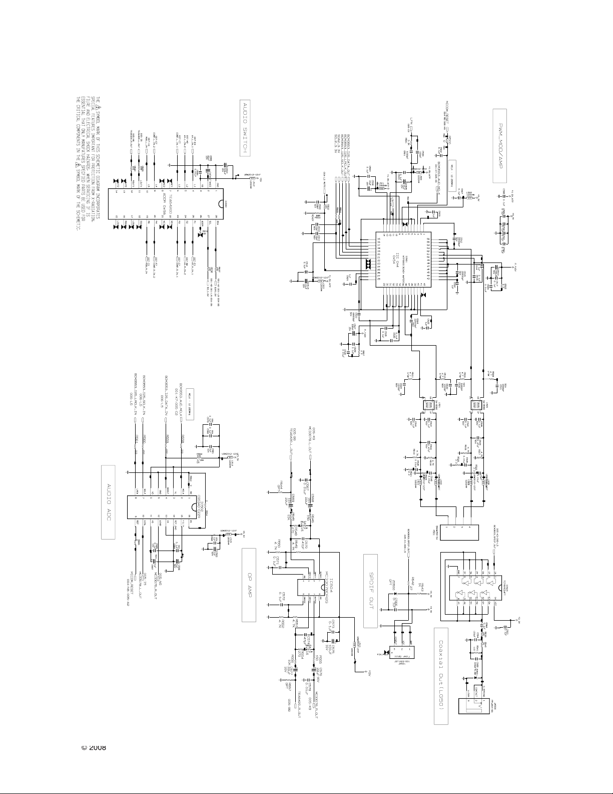
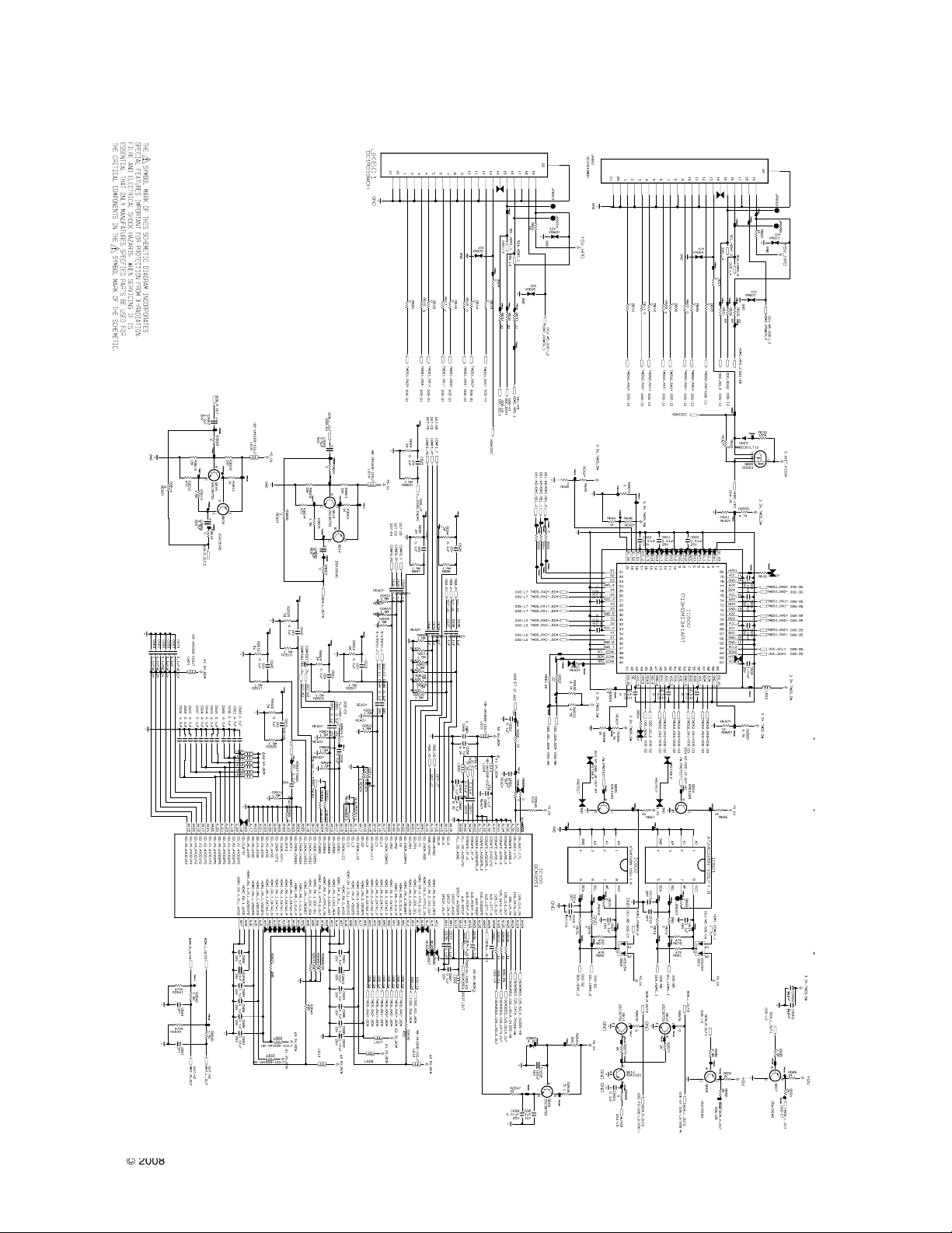
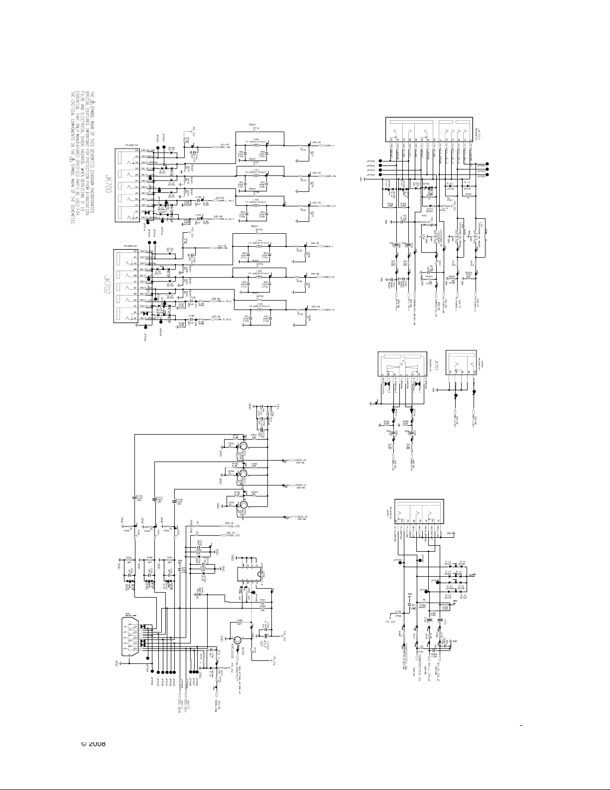
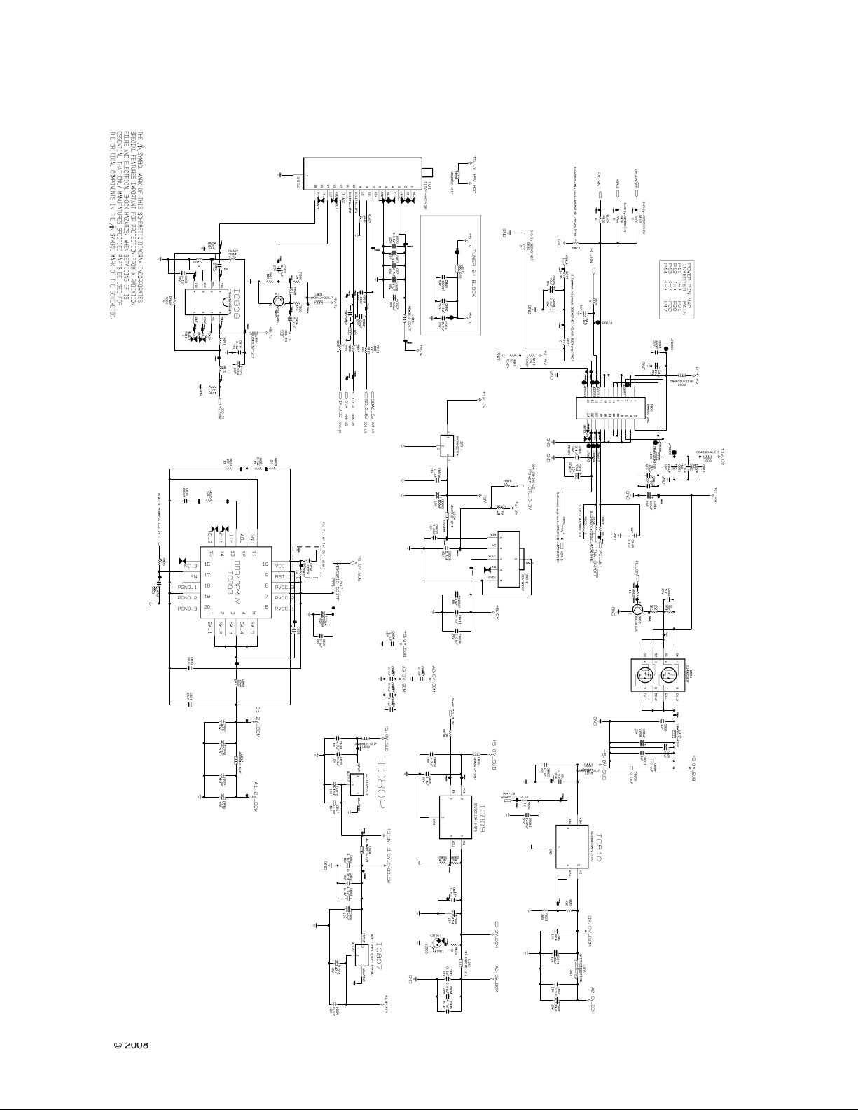
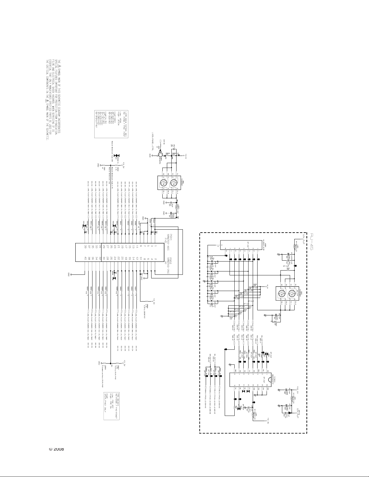
SCHEMA TIC DIAGRAM
Copyright LG Electronics. Inc. All right reserved.
Only for training and service purposes
LGE Internal Use Only
Page 31
Copyright LG Electronics. Inc. All right reserved.
Only for training and service purposes
LGE Internal Use Only
Page 32
Copyright LG Electronics. Inc. All right reserved.
Only for training and service purposes
LGE Internal Use Only
Page 33
Copyright LG Electronics. Inc. All right reserved.
Only for training and service purposes
LGE Internal Use Only
Page 34
Copyright LG Electronics. Inc. All right reserved.
Only for training and service purposes
LGE Internal Use Only
Page 35
Copyright LG Electronics. Inc. All right reserved.
Only for training and service purposes
LGE Internal Use Only
Page 36
Copyright LG Electronics. Inc. All right reserved.
Only for training and service purposes
LGE Internal Use Only
Page 37
Copyright LG Electronics. Inc. All right reserved.
Only for training and service purposes
LGE Internal Use Only
Page 38
Copyright LG Electronics. Inc. All right reserved.
Only for training and service purposes
LGE Internal Use Only
Page 39
Copyright LG Electronics. Inc. All right reserved.
Only for training and service purposes
LGE Internal Use Only
Page 40
Aug., 2008
Printed in KoreaP/NO : MFL41524424
 Loading...