

Page 1

Internal Use Only
LED TV
SERVICE MANUAL
CHASSIS : LA5CJ/LA5CG
MODEL : 43LX560H/570H
MODEL : 43LX560H/570H-U*
CAUTION
BEFORE SERVICING THE CHASSIS, READ THE SAFETY PRECAUTIONS IN THIS MANUAL.
P/NO : MFL69175103 (1611-REV01)
Page 2

CONTENTS
CONTENTS .............................................................................................. 2
SAFETY PRECAUTIONS ........................................................................ 3
SERVICING PRECAUTIONS ................................................................... 4
SPECIFICATION ...................................................................................... 6
USB DOWNLOAD ................................................................................... 8
TROUBLE SHOOTING GUIDE ................................................................ 9
BLOCK DIAGRAM ................................................................................. 17
EXPLODED VIEW .................................................................................. 18
Only for training and service purposes
- 2 -
LGE Internal Use OnlyCopyright © LG Electronics. Inc. All rights reserved.
Page 3
SAFETY PRECAUTIONS
IMPORTANT SAFETY NOTICE
Many electrical and mechanical parts in this chassis have special safety-related characteristics. These parts are identified by in the
Exploded View.
It is essential that these special safety parts should be replaced with the same components as recommended in this manual to prevent
Shock, Fire, or other Hazards.
Do not modify the original design without permission of manufacturer.
General Guidance
An isolation Transformer should always be used during the
servicing of a receiver whose chassis is not isolated from the AC
power line. Use a transformer of adequate power rating as this
protects the technician from accidents resulting in personal injury
from electrical shocks.
It will also protect the receiver and it's components from being
damaged by accidental shorts of the circuitry that may be
inadvertently introduced during the service operation.
If any fuse (or Fusible Resistor) in this TV receiver is blown,
replace it with the specified.
When replacing a high wattage resistor (Oxide Metal Film Resistor,
over 1 W), keep the resistor 10 mm away from PCB.
Keep wires away from high voltage or high temperature parts.
Before returning the receiver to the customer,
Always perform an AC leakage current check on the exposed
metallic parts of the cabinet, such as antennas, terminals, etc., to
be sure the set is safe to operate without damage of electrical
shock.
Leakage Current Cold Check(Antenna Cold Check)
With the instrument AC plug removed from AC source, connect an
electrical jumper across the two AC plug prongs. Place the AC
switch in the on position, connect one lead of ohm-meter to the AC
plug prongs tied together and touch other ohm-meter lead in turn to
each exposed metallic parts such as antenna terminals, phone
jacks, etc.
If the exposed metallic part has a return path to the chassis, the
measured resistance should be between 1 MΩ and 5.2 MΩ.
When the exposed metal has no return path to the chassis the
reading must be infinite.
An other abnormality exists that must be corrected before the
receiver is returned to the customer.
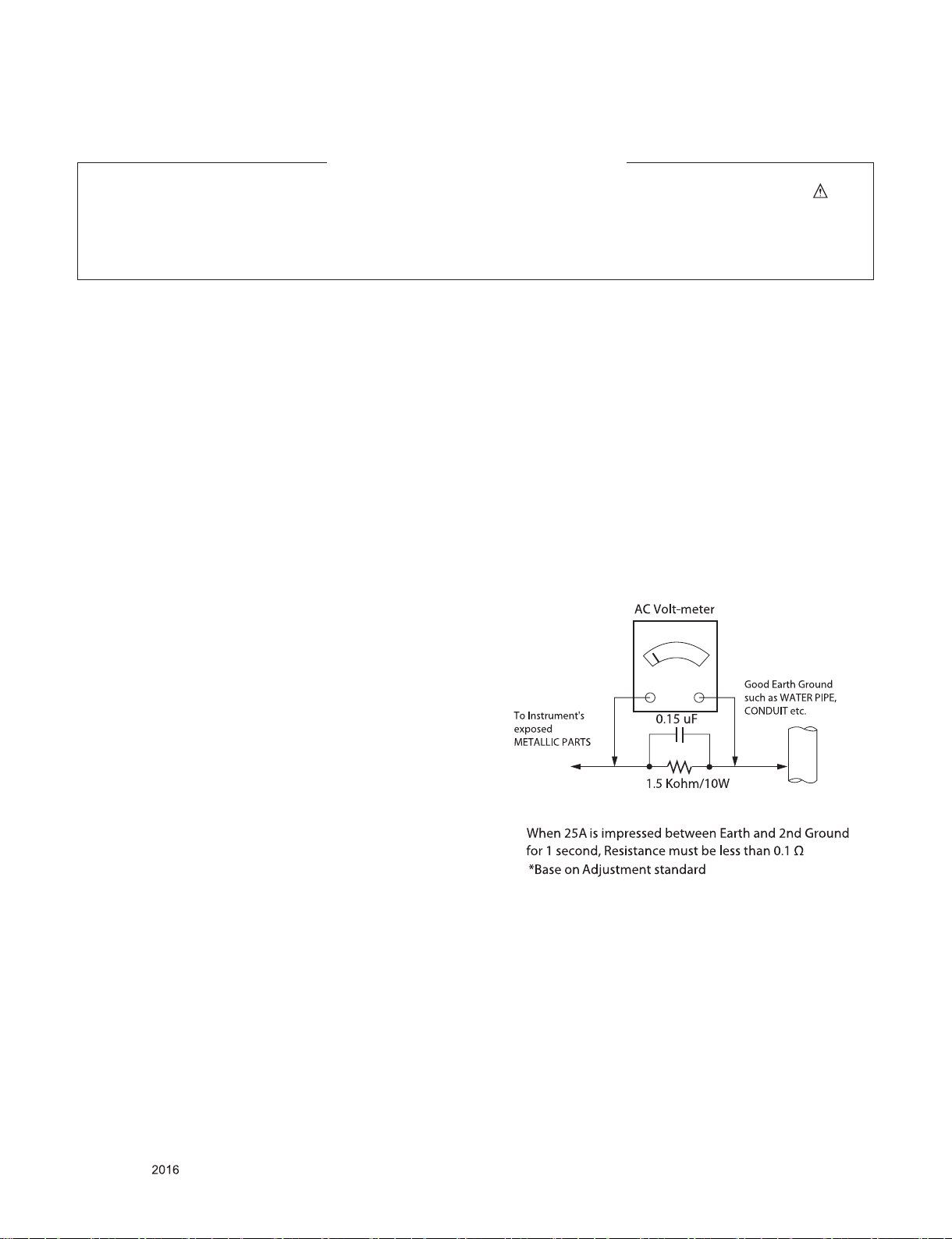
Leakage Current Hot Check (See below Figure)
Plug the AC cord directly into the AC outlet.
Do not use a line Isolation Transformer during this check.
Connect 1.5 K / 10 watt resistor in parallel with a 0.15 uF capacitor
between a known good earth ground (Water Pipe, Conduit, etc.)
and the exposed metallic parts.
Measure the AC voltage across the resistor using AC voltmeter
with 1000 ohms/volt or more sensitivity.
Reverse plug the AC cord into the AC outlet and repeat AC voltage
measurements for each exposed metallic part. Any voltage
measured must not exceed 0.75 volt RMS which is corresponds to
0.5 mA.
In case any measurement is out of the limits specified, there is
possibility of shock hazard and the set must be checked and
repaired before it is returned to the customer.
Leakage Current Hot Check circuit
Only for training and service purposes
- 3 -
LGE Internal Use OnlyCopyright © LG Electronics. Inc. All rights reserved.
Page 4

SERVICING PRECAUTIONS
CAUTION: Before servicing receivers covered by this service
manual and its supplements and addenda, read and follow the
SAFETY PRECAUTIONS on page 3 of this publication.
NOTE: If unforeseen circumstances create conict between the
following servicing precautions and any of the safety precautions
on page 3 of this publication, always follow the safety precautions. Remember: Safety First.
General Servicing Precautions
1. Always unplug the receiver AC power cord from the AC power
source before;
a. Removing or reinstalling any component, circuit board
module or any other receiver assembly.
b. Disconnecting or reconnecting any receiver electrical plug
or other electrical connection.
c. Connecting a test substitute in parallel with an electrolytic
capacitor in the receiver.
CAUTION: A wrong part substitution or incorrect polarity
installation of electrolytic capacitors may result in an explosion hazard.
2. Test high voltage only by measuring it with an appropriate
high voltage meter or other voltage measuring device (DVM,
FETVOM, etc) equipped with a suitable high voltage probe.
Do not test high voltage by "drawing an arc".
3. Do not spray chemicals on or near this receiver or any of its
assemblies.
4. Unless specied otherwise in this service manual, clean
electrical contacts only by applying the following mixture to the
contacts with a pipe cleaner, cotton-tipped stick or comparable
non-abrasive applicator; 10 % (by volume) Acetone and 90 %
(by volume) isopropyl alcohol (90 % - 99 % strength)
CAUTION: This is a ammable mixture.
Unless specied otherwise in this service manual, lubrication
of contacts in not required.
5. Do not defeat any plug/socket B+ voltage interlocks with which
receivers covered by this service manual might be equipped.
6. Do not apply AC power to this instrument and/or any of its
electrical assemblies unless all solid-state device heat sinks
are correctly installed.
7. Always connect the test receiver ground lead to the receiver
chassis ground before connecting the test receiver positive
lead.
Always remove the test receiver ground lead last.
8. Use with this receiver only the test xtures specied in this
service manual.
CAUTION: Do not connect the test xture ground strap to any
heat sink in this receiver.
Electrostatically Sensitive (ES) Devices
Some semiconductor (solid-state) devices can be damaged easily by static electricity. Such components commonly are called
Electrostatically Sensitive (ES) Devices. Examples of typical ES
devices are integrated circuits and some eld-effect transistors
and semiconductor “chip” components. The following techniques
should be used to help reduce the incidence of component damage caused by static by static electricity.
1. Immediately before handling any semiconductor component or
semiconductor-equipped assembly, drain off any electrostatic
charge on your body by touching a known earth ground. Alternatively, obtain and wear a commercially available discharging wrist strap device, which should be removed to prevent
potential shock reasons prior to applying power to the unit
under test.
2. After removing an electrical assembly equipped with ES
devices, place the assembly on a conductive surface such as
aluminum foil, to prevent electrostatic charge buildup or exposure of the assembly.
3. Use only a grounded-tip soldering iron to solder or unsolder
ES devices.
4. Use only an anti-static type solder removal device. Some sol-
der removal devices not classied as “anti-static” can generate
electrical charges sufcient to damage ES devices.
5. Do not use freon-propelled chemicals. These can generate
electrical charges sufcient to damage ES devices.
6. Do not remove a replacement ES device from its protective
package until immediately before you are ready to install it.
(Most replacement ES devices are packaged with leads electrically shorted together by conductive foam, aluminum foil or
comparable conductive material).
7. Immediately before removing the protective material from the
leads of a replacement ES device, touch the protective material to the chassis or circuit assembly into which the device will
be installed.
CAUTION: Be sure no power is applied to the chassis or circuit, and observe all other safety precautions.
8. Minimize bodily motions when handling unpackaged replacement ES devices. (Otherwise harmless motion such as the
brushing together of your clothes fabric or the lifting of your
foot from a carpeted oor can generate static electricity sufcient to damage an ES device.)
General Soldering Guidelines
1. Use a grounded-tip, low-wattage soldering iron and appropriate tip size and shape that will maintain tip temperature within
the range or 500 °F to 600 °F.
2. Use an appropriate gauge of RMA resin-core solder composed
of 60 parts tin/40 parts lead.
3. Keep the soldering iron tip clean and well tinned.
4. Thoroughly clean the surfaces to be soldered. Use a mall wirebristle (0.5 inch, or 1.25 cm) brush with a metal handle.
Do not use freon-propelled spray-on cleaners.
5. Use the following unsoldering technique
a. Allow the soldering iron tip to reach normal temperature.
(500 °F to 600 °F)
b. Heat the component lead until the solder melts.
c. Quickly draw the melted solder with an anti-static, suction-
type solder removal device or with solder braid.
CAUTION: Work quickly to avoid overheating the circuit
board printed foil.
6. Use the following soldering technique.
a. Allow the soldering iron tip to reach a normal temperature
(500 °F to 600 °F)
b. First, hold the soldering iron tip and solder the strand
against the component lead until the solder melts.
c. Quickly move the soldering iron tip to the junction of the
component lead and the printed circuit foil, and hold it there
only until the solder ows onto and around both the component lead and the foil.
CAUTION: Work quickly to avoid overheating the circuit
board printed foil.
d. Closely inspect the solder area and remove any excess or
splashed solder with a small wire-bristle brush.
Only for training and service purposes
- 4 -
LGE Internal Use OnlyCopyright © LG Electronics. Inc. All rights reserved.
Page 5

IC Remove/Replacement
Some chassis circuit boards have slotted holes (oblong) through
which the IC leads are inserted and then bent at against the circuit foil. When holes are the slotted type, the following technique
should be used to remove and replace the IC. When working with
boards using the familiar round hole, use the standard technique
as outlined in paragraphs 5 and 6 above.
Removal
1. Desolder and straighten each IC lead in one operation by
gently prying up on the lead with the soldering iron tip as the
solder melts.
2. Draw away the melted solder with an anti-static suction-type
solder removal device (or with solder braid) before removing
the IC.
Replacement
1. Carefully insert the replacement IC in the circuit board.
2. Carefully bend each IC lead against the circuit foil pad and
solder it.
3. Clean the soldered areas with a small wire-bristle brush.
(It is not necessary to reapply acrylic coating to the areas).
"Small-Signal" Discrete Transistor
Removal/Replacement
1. Remove the defective transistor by clipping its leads as close
as possible to the component body.
2. Bend into a "U" shape the end of each of three leads remaining on the circuit board.
3. Bend into a "U" shape the replacement transistor leads.
4. Connect the replacement transistor leads to the corresponding
leads extending from the circuit board and crimp the "U" with
long nose pliers to insure metal to metal contact then solder
each connection.
Power Output, Transistor Device
Removal/Replacement
1. Heat and remove all solder from around the transistor leads.
2. Remove the heat sink mounting screw (if so equipped).
3. Carefully remove the transistor from the heat sink of the circuit
board.
4. Insert new transistor in the circuit board.
5. Solder each transistor lead, and clip off excess lead.
6. Replace heat sink.
Diode Removal/Replacement
1. Remove defective diode by clipping its leads as close as possible to diode body.
2. Bend the two remaining leads perpendicular y to the circuit
board.
3. Observing diode polarity, wrap each lead of the new diode
around the corresponding lead on the circuit board.
4. Securely crimp each connection and solder it.
5. Inspect (on the circuit board copper side) the solder joints of
the two "original" leads. If they are not shiny, reheat them and
if necessary, apply additional solder.
3. Solder the connections.
CAUTION: Maintain original spacing between the replaced
component and adjacent components and the circuit board to
prevent excessive component temperatures.
Circuit Board Foil Repair
Excessive heat applied to the copper foil of any printed circuit
board will weaken the adhesive that bonds the foil to the circuit
board causing the foil to separate from or "lift-off" the board. The
following guidelines and procedures should be followed whenever this condition is encountered.
At IC Connections
To repair a defective copper pattern at IC connections use the
following procedure to install a jumper wire on the copper pattern
side of the circuit board. (Use this technique only on IC connections).
1. Carefully remove the damaged copper pattern with a sharp
knife. (Remove only as much copper as absolutely necessary).
2. Carefully scratch away the solder resist and acrylic coating (if
used) from the end of the remaining copper pattern.
3. Bend a small "U" in one end of a small gauge jumper wire and
carefully crimp it around the IC pin. Solder the IC connection.
4. Route the jumper wire along the path of the out-away copper
pattern and let it overlap the previously scraped end of the
good copper pattern. Solder the overlapped area and clip off
any excess jumper wire.
At Other Connections
Use the following technique to repair the defective copper pattern
at connections other than IC Pins. This technique involves the
installation of a jumper wire on the component side of the circuit
board.
1. Remove the defective copper pattern with a sharp knife.
Remove at least 1/4 inch of copper, to ensure that a hazardous
condition will not exist if the jumper wire opens.
2. Trace along the copper pattern from both sides of the pattern
break and locate the nearest component that is directly connected to the affected copper pattern.
3. Connect insulated 20-gauge jumper wire from the lead of the
nearest component on one side of the pattern break to the
lead of the nearest component on the other side.
Carefully crimp and solder the connections.
CAUTION: Be sure the insulated jumper wire is dressed so the
it does not touch components or sharp edges.
Fuse and Conventional Resistor
Removal/Replacement
1. Clip each fuse or resistor lead at top of the circuit board hollow
stake.
2. Securely crimp the leads of replacement component around
notch at stake top.
Only for training and service purposes
- 5 -
LGE Internal Use OnlyCopyright © LG Electronics. Inc. All rights reserved.
Page 6
SPECIFICATION
NOTE : Specifications and others are subject to change without notice for improvement
.
1. Application range
This specification is applied to the LED TV used LA5CJ/
LA5CG chassis.
2. Requirement for Test
Each part is tested as below without special appointment.
1) Temperature: 25 °C ± 5 °C(77 °F ± 9 °F), CST: 40 °C ± 5 °C
2) Relative Humidity: 65 % ± 10 %
3) Power Voltage
: Standard input voltage (AC 100-240 V~, 50/60 Hz)
* Standard Voltage of each products is marked by models.
4) Specification and performance of each parts are followed
each drawing and specification by part number in
accordance with BOM.
5) The receiver must be operated for about 5 minutes prior to
the adjustment.
3. Test method
1) Performance: LGE TV test method followed
2) Demanded other specification
- Safety : CE, IEC specification
- EMC : CE, IEC
4. Model General Specification
No. Item Specication Remarks
1 Receiving System ATSC / NTSC-M / 64 QAM / 256 QAM North America
1) VHF : 02~13
2) UHF : 14~69
2 Available Channel
3 Input Voltage North America
4 Market North America
5 Screen Size
6 Aspect Ratio 16:9
7 Tuning System FS
8 Module
9 Operating Environment
10 Storage Environment
3) DTV : 02-69
4) CATV : 01~135
5) CADTV : 01~135
AC 100 ~ 240V@
50/60Hz
28 inch Wide (1366 × 768) HD + 60Hz
32 inch Wide (1920 × 1080) FHD + 60Hz
40 inch Wide (1920 × 1080) FHD + 60Hz
43 inch Wide (1920 × 1080) FHD + T120Hz
49 inch Wide (1920 × 1080) FHD + T120Hz
55 Inch Wide (1920 × 1080) FHD + T120Hz
65 Inch Wide (1920 x 1080) FHD + T240Hz
HC275EXN-VSDP1 28LX570H-UA
LC320DUE-FHA3 32LX570H/560H-UA
HC400DUN-VCKN5 40LX570H/560H-UA
LC430EUE-FHM3 43LX570H/560H-UA
LC490EUE-FHM3 49LX570H/560H-UA
LC550EUE-FHM3 55LX570H-UA
LC650EUF-FHM3 65LX570H-UA
1) Temp : 0 ~ 40 deg
2) Humidity : ~ 80 %
1) Temp. : -20 ~ 60 deg
2) Humidity : ~ 85%
Mark : 110V, 60Hz (N.America)
Only for training and service purposes
- 6 -
LGE Internal Use OnlyCopyright © LG Electronics. Inc. All rights reserved.
Page 7

5. Video resolutions
5.1. HDMI Input(PC/DTV)
No. Resolution H-freq(kHz) V-freq.(Hz) Pixel clock(MHz) Proposed Remark
PC DDC
1
2
3
4
5
6
7
8
9
DTV
1 720*480 31.500 60.000 27.027 SDTV 480P
2 720*480 31.470 59.940 27.000 SDTV 480P
3 1280*720 45.000 60.000 74.250 HDTV 720P
4 1280*720 44.960 59.940 74.176 HDTV 720P
5 1920*1080 33.750 60.000 74.250 HDTV 1080I
6 1920*1080 33.720 59.940 74.176 HDTV 1080I
7 1920*1080 67.500 60.000 148.500 HDTV 1080P
8 1920*1080 67.4320 59.940 148.352 HDTV 1080P
9 1920*1080 27.000 24.000 74.250 HDTV 1080P
10 1920*1080 26.970 23.976 74.176 HDTV 1080P
11 1920*1080 33.750 30.000 74.250 HDTV 1080P
12 1920*1080 33.710 29.970 74.176 HDTV 1080P
640*350 31.468 70.09 25.17
720*400 31.469 70.08 28.32
640*480 31.469 59.94 25.17
800*600 37.879 60.31 40.00
1024*768 48.363 60.00 60.00
1152*864 54.348 60.053
1280*1024 63.981 60.020 108.0
1360*768 47.712 60.015 85.50
1920*1080 67.50 60.00 148.5
EGA X
DOS O
VESA(VGA) O
VESA(SVGA) O
VESA(XGA) O
VESA X
VESA (SXGA) O
VESA (WXGA) O
HDTV 1080P O
5.2. RGB input(PC)
No. Resolution H-freq(kHz) V-freq.(Hz) Pixel clock(MHz) Proposed Remark
PC DDC
1 640*350 31.468 70.09 25.17 EGA Х
2 720*400 31.469 70.08 28.32 DOS O
3 640*480 31.469 59.94 25.17 VESA(VGA) O
4 800*600 37.879 60.31 40.00 VESA(SVGA) O
5 1024*768 48.363 60.00 65.00 VESA(XGA) O
6 1280*768 47.776 59.870 79.5 CVT(WXGA) Х
7 1360*768 47.712 60.015 85.50 VESA (WXGA) Х
8 1600*1200 75.00 60.00 162.0 VESA (UXGA) X
9 1920*1080 67.50 60.00 148.5 HDTV 1080P O
Only for training and service purposes
- 7 -
LGE Internal Use OnlyCopyright © LG Electronics. Inc. All rights reserved.
Page 8

USB DOWNLOAD
(1) Put the USB Stick to the USB socket
(2) Automatically detecting update file in USB Stick
- If your downloaded program version in USB Stick is Lower, it didn’t work.
But your downloaded version is Higher, USB data is automatically detecting (Download Version High & Power only mode, Set is
automatically Download)
(3) Show the message “Copying files from memory”
(4) Updating is starting.
(5) Updating Completed, the TV will restart automatically.
(6) If your TV is turned on, check your updated version and Tool option. (explain the Tool option, next stage)
* If downloading version is more high than your TV have, TV can lost all channel data. In this case, you have to channel recover.
if all channel data is cleared, you didn’t have a DTV/ATV test on production line.
* After downloading, have to adjust Tool Option again.
(1) Push "IN-START" key in service remote control.
(2) Select "Tool Option 1" and push "OK" key.
(3) Punch in the number. (Each model has their number)
Only for training and service purposes
- 8 -
LGE Internal Use OnlyCopyright © LG Electronics. Inc. All rights reserved.
Page 9

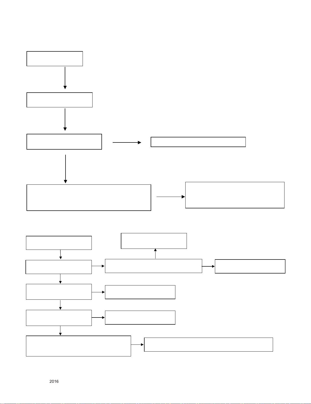
TROUBLE SHOOTING GUIDE
Ch eck P401 Voltag e Level
(13.2V, L403)
Ch eck p ower co nnector and RL_ON
signal OK ?
Rep lace Po wer board
Y
N Y
Ch eck IC5002
RESET and U PDATE p in
Ch eck switch SW501, SW 502
Y
N
Ch eck X5000 Cloc k
32.768KHz
Ch eck X5000 ap plicati on circuit o r
Rep lace X5000
Y
N
Ch eck IC5002 IIC
co mmunication state
Ch eck IIC l ine or rep lace IC5002
N
Ch eck IR i nput state of IC5002
57pin
Ch eck IR bo ard
N
Y
Re-d ownload PTC Micom
Y
Ch eck LVDS Cable
Ch eck LCD Mo dule
Co ntrol bo ard
Y
Rep lace Cabl e
N
Ch eck P401 Voltag e Level
(13.2V, L403)
Ch eck p ower co nnector and
RL_ON(pin1) signal OK ?
Rep lace Po wer board
N Y
Ch eck Q405 outp ut Voltage(12V)
Y
Ch eck Q405 app lic ation circuit o r
rep lace Q 405
N
1. Power-Up Boot Fail Trouble Shooting guide
2. No OSD Trouble Shooting guide
Only for training and service purposes
- 9 -
LGE Internal Use OnlyCopyright © LG Electronics. Inc. All rights reserved.
Page 10

3. Analog RF Video Trouble Shooting guide
Ch eck TU3001 Pin7(Video o utput)
Can you s ee the n ormal s ignal?
Ch eck tun er 5V po wer L3000
YES
NO
Co uld y ou measure v oltage of T U3001 & IIC lines ?
Are th ey all no rmal?
Ch eck Mstar LVDS outp ut
NO
You s ho uld check p ower line
& IIC l ines.
YES
You s ho uld repl ace T UNER.
NO
Ch eck IC5000
YES
YES
Ch eck tun er 3.3V po wer L3001 Replace L3001
NO
Rep lace IC5000
Rep lace L3000
YES
NO
Ch eck tun er 1.8V po wer L3003
Rep lace IC3000 o r IC3000
NO
Ch eck RF cable & s ignal
YES
NO
Rep lace Ms tar(IC101)
or main board
Only for training and service purposes
- 10 -
LGE Internal Use OnlyCopyright © LG Electronics. Inc. All rights reserved.
Page 11

4. Digital RF Trouble Shooting guide
Ch eck RF Cable
Ch eck IIC Si gnal
TU3001 #3, 4Pin
Ch eck IIC l in e and level shifter c ir cui t
Y
N
Ch eck Tun er 5V Power
L3000
Ch eck L3000
Y
N
Y
Ch eck X201
and ap pl ication circuit
Ch eck IF Si gnal
TU3001 #10, 11 Pi n
Ch eck tun er applic ation circuit o r
rep lace tun er.
N
Y
Rep lace X201
N
Y
Rep lace IC101
Rep lace IC5000
N
Y
Rep lace L3000
Only for training and service purposes
- 11 -
LGE Internal Use OnlyCopyright © LG Electronics. Inc. All rights reserved.
Page 12

5. AV Video Trouble Shooting guide
Ch eck JK5001
Can you s ee the n ormal waveform?
N
JK5001 may hav e pro blem. Repl ace th is Jack.
Ch eck th e in put of Mstar( IC101).
Measure wavefo rm at C227 becaus e it’s mo re easy to c heck.
Can you s ee the n ormal waveform?
Y
Th is bo ard h as bi g problem
becaus e Main chip (Mstar) have some troubles.
After chec king th oroughly all p ath once again,
You s ho uld d ecide to replace Mstar or not.
Y
Ch eck input s ignal i s s upported format
Y
Ch eck AC cable fo r damage o r o pen conductor
Y
Only for training and service purposes
- 12 -
LGE Internal Use OnlyCopyright © LG Electronics. Inc. All rights reserved.
Page 13

6. HDMI Video Trouble Shooting guide
Check JK800/JK801/JK802
Can yo u see th e no rmal waveform?
N
JK800/JK801/JK802 may h ave p roblem. Repl ace th is Jack.
Th is bo ard has big p roblem because Main chip (Mstar) have some troubles.
After checking th oroughly all path o nce again, You sh ould d ecide to replace Mstar o r n ot.
Check in put signal format.
Is i t supported?
Y
Check AC cabl e for damage
Fo r damage o r o pen co nductor
Y
Y
Check HDMI Switch IC Power
Check L800(3.3V, No t stan d-by mode)
Y
Swap HDMI Switch IC,
is there same Pro blem?
Y
N
Replac e L800
Only for training and service purposes
- 13 -
LGE Internal Use OnlyCopyright © LG Electronics. Inc. All rights reserved.
Page 14
7. RGB-PC Video Trouble shooting guide
Check P3300
Can yo u see th e no rmal waveform?
NO
P3300 may h ave problem. Rep lace this Jac k.
Check the in put of Mstar(IC101).
Measure wavefo rm at R234, R235
becaus e it’s mo re easy to c heck.
Can yo u see th e no rmal waveform?
YES
Th is bo ard has big problem
because Mai n chip (Ms tar) have so me troubles.
After chec king th oroughly all p ath once again,
You sh oul d decide to replace Mstar or not.
YES
Check in put signal fo rmat.
Is i t suppo rted?
YES
Check AC cable for damage
Fo r damage o r o pen co nductor
YES
Ch eck RF C able & Sig nal
Ch eck Aud io AMP outp ut
L5503,L5504,L5505,L5506
Y
Ch eck TU3001 Pi n1 (SIF Output)
Can you s ee the n ormal s ignal?
Y
Co uld y ou measure v oltage of T U3001& IIC lines ?
Are th ey all no rmal?
N
You s ho uld check p ower line & IIC lin es.
N
You s ho uld repl ace TUNER.
Y
Ch eck IC5600
Y
Rep lace IC5600
N
Rep lace L5503,L5504,L5505,L5506
N
Ch eck th e in put of Mstar (IC101).
Measure w avefor m at C115, C116 becaus e it’s mo re easy to
check.
Can you s ee the n ormal wav eform?
Y
After ch eck ing audio s ignal line, y ou sh ould d eci de to r eplac e item o r n ot.
N
8. Analog RF Audio Trouble Shooting guide
Only for training and service purposes
- 14 -
LGE Internal Use OnlyCopyright © LG Electronics. Inc. All rights reserved.
Page 15

9. AV/RGB-PC Audio in Trouble shooting guide
Check in put signal fo rmat.
Is i t supported?
Check P3300, JK5001
Can yo u see th e no rmal waveform?
Replac e P3300, J K5001
Y
N
Check AC cable for d amage
Fo r damage o r o pen co nductor
Y
Y
Check the in put of Mstar(IC101).
Measure wavefo rm at C209, C211 because i t’s more easy to check.
Can yo u see th e no rmal waveform?
Y
Check Audi o AMP output
L5503,L5504,L5505,L5506
Y
Replac e L5503,L5504,L5505,L5506
N
Th is bo ard has big p roblem because Main chip (Ms tar) have so me troubles.
After checking th oroughly all path o nce again, You should dec ide to replace Mstar or n ot.
- 15 -
Only for training and service purposes
LGE Internal Use OnlyCopyright © LG Electronics. Inc. All rights reserved.
Page 16

10. HDMI Audio in Trouble Shooting guide
Check in put signal fo rmat.
Is i t suppo rted?
Check JK800/JK801/JK802
Can yo u see th e no rmal waveform?
Replace JK800/JK801/JK802
Y
N
Check AC cable for damage
Fo r damage o r o pen co nductor
Y
Y
Check Audi o AMP o utput
L5503,L5504,L5505,L5506
Y
Replace L5503,L5504,L5505,L5506
N
Th is bo ard has big problem becaus e Main c hip ( Mstar) have so me troubles.
After chec king th oroughly all p ath once again, You should d ecide to replace Mstar or not.
Ch eck th e output o f Mstar(IC101).
Measur e wavefor m at R123, IC5600(Pin 23, 24).
becaus e it’s mo re easy to ch eck. Can yo u see th e normal s ignal ?
YES
NO
Th is bo ard h as bi g pr oblem bec ause Main c hip (MStar) h ave so me tr oubles.
After ch eck ing thoroughl y al l p ath once again,
You s ho uld d ecide to rep lac e Mstar or not.
Ch eck Aud io AMP outp ut L5503,L5504,L5505,L5506
Can you s ee the n ormal wav eform?
NO
YES
After ch eck ing the Po wer & I2C & Reset o f this ch ip,
yo u sh ould deci de to replac e this or n ot.
Ch eck th e sp eaker o utput wafer P5600.
Can you s ee the n ormal wav eform?
NO
YES
After ch eck ing audio s ignal line, y ou sh ould d eci de to r eplac e item o r n ot.
Ch eck th e co nnector & Speak er
11. Audio out Trouble shooting guide
Only for training and service purposes
- 16 -
LGE Internal Use OnlyCopyright © LG Electronics. Inc. All rights reserved.
Page 17

BLOCK DIAGRAM
Only for training and service purposes
- 17 -
LGE Internal Use OnlyCopyright © LG Electronics. Inc. All rights reserved.
Page 18

EXPLODED VIEW
Many electrical and mechanical parts in this chassis have special safety-related characteristics. These
parts are identified by in the EXPLODED VIEW.
It is essential that these special safety parts should be replaced with the same components as
recommended in this manual to prevent Shock, Fire, or other Hazards.
Do not modify the original design without permission of manufacturer.
400
IMPORTANT SAFETY NOTICE
910
900
350
120
800
810
521
540
121
530
LV1
820
200
Only for training and service purposes
- 18 -
A2
A10
Set + Stand
LGE Internal Use OnlyCopyright © LG Electronics. Inc. All rights reserved.
Page 19

 Loading...