

Page 1
Internal Use Only
North/Latin America http://aic.lgservice.com
Europe/Africa http://eic.lgservice.com
Asia/Oceania http://biz.lgservice.com
LED TV
SERVICE MANUAL
CHASSIS : LJ55A
MODEL : 43LF5100 43LF5100-SA
49LF5100 49LF5100-SA
CAUTION
BEFORE SERVICING THE CHASSIS,
READ THE SAFETY PRECAUTIONS IN THIS MANUAL.
Printed in KoreaP/NO : MFL68606519 (1505-REV00)
Page 2

CONTENTS
CONTENTS .............................................................................................. 2
PRODUCT SAFETY ................................................................................. 3
SPECIFICATION ....................................................................................... 6
ADJUSTMENT INSTRUCTION ................................................................ 9
DISASSEMBLY ........................................................................................ 15
BLOCK DIAGRAM ...................................................................................16
EXPLODED VIEW .................................................................................. 17
SCHEMATIC CIRCUIT DIAGRAM ............................................APPENDIX
TROUBLESHOOTING ...............................................................APPENDIX
Only for training and service purposes
- 2 -
LGE Internal Use OnlyCopyright © LG Electronics. Inc. All rights reserved.
Page 3
SAFETY PRECAUTIONS
IMPORTANT SAFETY NOTICE
Many electrical and mechanical parts in this chassis have special safety-related characteristics. These parts are identified by in the
Schematic Diagram and Exploded View.
It is essential that these special safety parts should be replaced with the same components as recommended in this manual to prevent
Shock, Fire, or other Hazards.
Do not modify the original design without permission of manufacturer.
General Guidance
An isolation Transformer should always be used during the
servicing of a receiver whose chassis is not isolated from the AC
power line. Use a transformer of adequate power rating as this
protects the technician from accidents resulting in personal injury
from electrical shocks.
It will also protect the receiver and it's components from being
damaged by accidental shorts of the circuitry that may be
inadvertently introduced during the service operation.
If any fuse (or Fusible Resistor) in this TV receiver is blown,
replace it with the specified.
When replacing a high wattage resistor (Oxide Metal Film Resistor,
over 1 W), keep the resistor 10 mm away from PCB.
Keep wires away from high voltage or high temperature parts.
Before returning the receiver to the customer,
always perform an AC leakage current check on the exposed
metallic parts of the cabinet, such as antennas, terminals, etc., to
be sure the set is safe to operate without damage of electrical
shock.
Leakage Current Cold Check(Antenna Cold Check)
With the instrument AC plug removed from AC source, connect an
electrical jumper across the two AC plug prongs. Place the AC
switch in the on position, connect one lead of ohm-meter to the AC
plug prongs tied together and touch other ohm-meter lead in turn to
each exposed metallic parts such as antenna terminals, phone
jacks, etc.
If the exposed metallic part has a return path to the chassis, the
measured resistance should be between 1 MΩ and 5.2 MΩ.
When the exposed metal has no return path to the chassis the
reading must be infinite.
An other abnormality exists that must be corrected before the
receiver is returned to the customer.
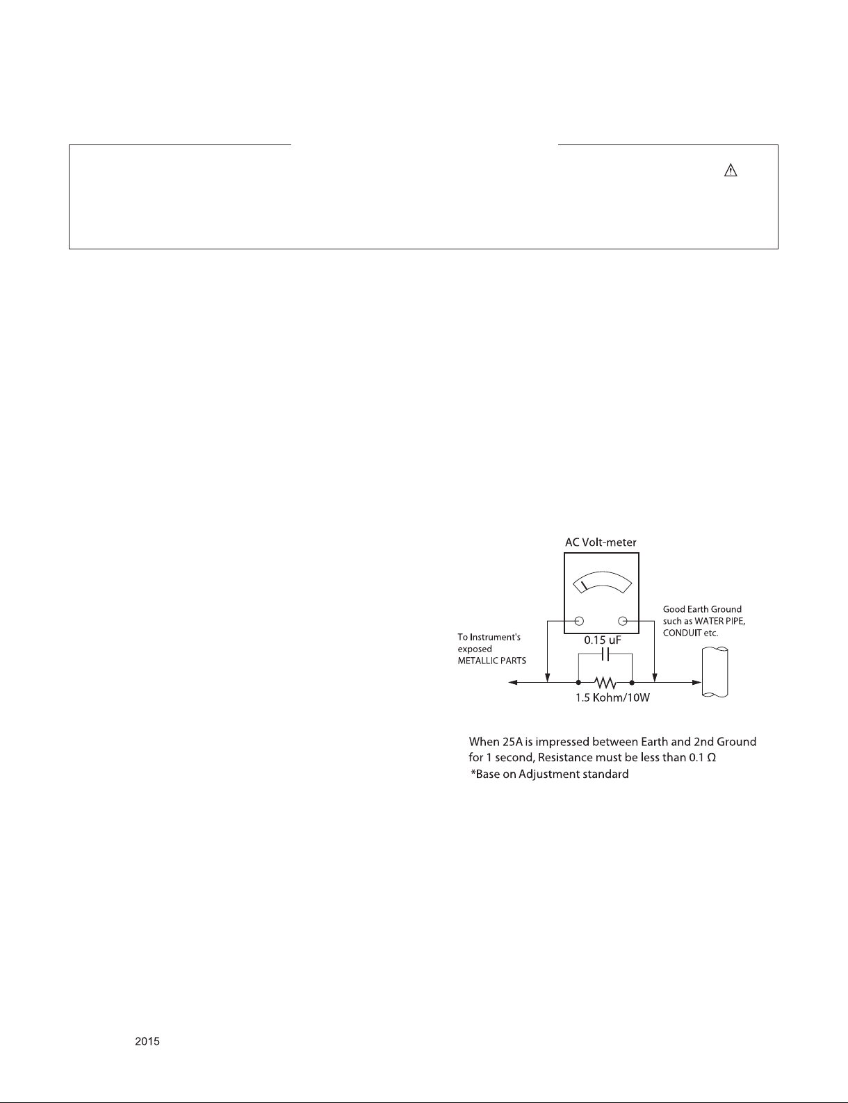
Leakage Current Hot Check (See below Figure)
Plug the AC cord directly into the AC outlet.
Do not use a line Isolation Transformer during this check.
Connect 1.5 K / 10 watt resistor in parallel with a 0.15 uF capacitor
between a known good earth ground (Water Pipe, Conduit, etc.)
and the exposed metallic parts.
Measure the AC voltage across the resistor using AC voltmeter
with 1000 ohms/volt or more sensitivity.
Reverse plug the AC cord into the AC outlet and repeat AC voltage
measurements for each exposed metallic part. Any voltage
measured must not exceed 0.75 volt RMS which is corresponds to
0.5 mA.
In case any measurement is out of the limits specified, there is
possibility of shock hazard and the set must be checked and
repaired before it is returned to the customer.
Leakage Current Hot Check circuit
Only for training and service purposes
- 3 -
LGE Internal Use OnlyCopyright © LG Electronics. Inc. All rights reserved.
Page 4

SERVICING PRECAUTIONS
CAUTION: Before servicing receivers covered by this service
manual and its supplements and addenda, read and follow the
SAFETY PRECAUTIONS on page 3 of this publication.
NOTE: If unforeseen circumstances create conict between the
following servicing precautions and any of the safety precautions
on page 3 of this publication, always follow the safety precautions.
Remember: Safety First.
General Servicing Precautions
1. Always unplug the receiver AC power cord from the AC power
source before;
a. Removing or reinstalling any component, circuit board mod-
ule or any other receiver assembly.
b. Disconnecting or reconnecting any receiver electrical plug or
other electrical connection.
c. Connecting a test substitute in parallel with an electrolytic
capacitor in the receiver.
CAUTION: A wrong part substitution or incorrect polarity
installation of electrolytic capacitors may result in an explosion hazard.
2. Test high voltage only by measuring it with an appropriate
high voltage meter or other voltage measuring device (DVM,
FETVOM, etc) equipped with a suitable high voltage probe.
Do not test high voltage by "drawing an arc".
3. Do not spray chemicals on or near this receiver or any of its
assemblies.
4. Unless specied otherwise in this service manual, clean
electrical contacts only by applying the following mixture to the
contacts with a pipe cleaner, cotton-tipped stick or comparable
non-abrasive applicator; 10 % (by volume) Acetone and 90 %
(by volume) isopropyl alcohol (90 % - 99 % strength)
CAUTION: This is a ammable mixture.
Unless specied otherwise in this service manual, lubrication of
contacts in not required.
5. Do not defeat any plug/socket B+ voltage interlocks with which
receivers covered by this service manual might be equipped.
6. Do not apply AC power to this instrument and/or any of its
electrical assemblies unless all solid-state device heat sinks are
correctly installed.
7. Always connect the test receiver ground lead to the receiver
chassis ground before connecting the test receiver positive
lead.
Always remove the test receiver ground lead last.
8. Use with this receiver only the test xtures specied in this
service manual.
CAUTION: Do not connect the test xture ground strap to any
heat sink in this receiver.
Electrostatically Sensitive (ES) Devices
Some semiconductor (solid-state) devices can be damaged easily by static electricity. Such components commonly are called
Electrostatically Sensitive (ES) Devices. Examples of typical ES
devices are integrated circuits and some eld-effect transistors
and semiconductor “chip” components. The following techniques
should be used to help reduce the incidence of component damage caused by static by static electricity.
1. Immediately before handling any semiconductor component or
semiconductor-equipped assembly, drain off any electrostatic
charge on your body by touching a known earth ground. Alternatively, obtain and wear a commercially available discharging
wrist strap device, which should be removed to prevent potential shock reasons prior to applying power to the unit under test.
2. After removing an electrical assembly equipped with ES
devices, place the assembly on a conductive surface such as
aluminum foil, to prevent electrostatic charge buildup or exposure of the assembly.
3. Use only a grounded-tip soldering iron to solder or unsolder ES
devices.
4. Use only an anti-static type solder removal device. Some solder
removal devices not classied as “anti-static” can generate
electrical charges sufcient to damage ES devices.
5. Do not use freon-propelled chemicals. These can generate
electrical charges sufcient to damage ES devices.
6. Do not remove a replacement ES device from its protective
package until immediately before you are ready to install it.
(Most replacement ES devices are packaged with leads electrically shorted together by conductive foam, aluminum foil or
comparable conductive material).
7. Immediately before removing the protective material from the
leads of a replacement ES device, touch the protective material
to the chassis or circuit assembly into which the device will be
installed.
CAUTION: Be sure no power is applied to the chassis or circuit,
and observe all other safety precautions.
8. Minimize bodily motions when handling unpackaged replacement ES devices. (Otherwise harmless motion such as the
brushing together of your clothes fabric or the lifting of your
foot from a carpeted oor can generate static electricity sufcient to damage an ES device.)
General Soldering Guidelines
1. Use a grounded-tip, low-wattage soldering iron and appropriate
tip size and shape that will maintain tip temperature within the
range or 500 °F to 600 °F.
2. Use an appropriate gauge of RMA resin-core solder composed
of 60 parts tin/40 parts lead.
3. Keep the soldering iron tip clean and well tinned.
4. Thoroughly clean the surfaces to be soldered. Use a mall wirebristle (0.5 inch, or 1.25 cm) brush with a metal handle.
Do not use freon-propelled spray-on cleaners.
5. Use the following unsoldering technique
a. Allow the soldering iron tip to reach normal temperature.
(500 °F to 600 °F)
b. Heat the component lead until the solder melts.
c. Quickly draw the melted solder with an anti-static, suction-
type solder removal device or with solder braid.
CAUTION: Work quickly to avoid overheating the circuit
board printed foil.
6. Use the following soldering technique.
a. Allow the soldering iron tip to reach a normal temperature
(500 °F to 600 °F)
b. First, hold the soldering iron tip and solder the strand against
the component lead until the solder melts.
c. Quickly move the soldering iron tip to the junction of the
component lead and the printed circuit foil, and hold it there
only until the solder ows onto and around both the component lead and the foil.
CAUTION: Work quickly to avoid overheating the circuit
board printed foil.
d. Closely inspect the solder area and remove any excess or
splashed solder with a small wire-bristle brush.
Only for training and service purposes
- 4 -
LGE Internal Use OnlyCopyright © LG Electronics. Inc. All rights reserved.
Page 5

IC Remove/Replacement
Some chassis circuit boards have slotted holes (oblong) through
which the IC leads are inserted and then bent at against the circuit foil. When holes are the slotted type, the following technique
should be used to remove and replace the IC. When working with
boards using the familiar round hole, use the standard technique
as outlined in paragraphs 5 and 6 above.
Removal
1. Desolder and straighten each IC lead in one operation by
gently prying up on the lead with the soldering iron tip as the
solder melts.
2. Draw away the melted solder with an anti-static suction-type
solder removal device (or with solder braid) before removing
the IC.
Replacement
1. Carefully insert the replacement IC in the circuit board.
2. Carefully bend each IC lead against the circuit foil pad and
solder it.
3. Clean the soldered areas with a small wire-bristle brush.
(It is not necessary to reapply acrylic coating to the areas).
"Small-Signal" Discrete Transistor
Removal/Replacement
1. Remove the defective transistor by clipping its leads as close
as possible to the component body.
2. Bend into a "U" shape the end of each of three leads remaining
on the circuit board.
3. Bend into a "U" shape the replacement transistor leads.
4. Connect the replacement transistor leads to the corresponding
leads extending from the circuit board and crimp the "U" with
long nose pliers to insure metal to metal contact then solder
each connection.
Power Output, Transistor Device
Removal/Replacement
1. Heat and remove all solder from around the transistor leads.
2. Remove the heat sink mounting screw (if so equipped).
3. Carefully remove the transistor from the heat sink of the circuit
board.
4. Insert new transistor in the circuit board.
5. Solder each transistor lead, and clip off excess lead.
6. Replace heat sink.
Diode Removal/Replacement
1. Remove defective diode by clipping its leads as close as possible to diode body.
2. Bend the two remaining leads perpendicular y to the circuit
board.
3. Observing diode polarity, wrap each lead of the new diode
around the corresponding lead on the circuit board.
4. Securely crimp each connection and solder it.
5. Inspect (on the circuit board copper side) the solder joints of
the two "original" leads. If they are not shiny, reheat them and if
necessary, apply additional solder.
3. Solder the connections.
CAUTION: Maintain original spacing between the replaced
component and adjacent components and the circuit board to
prevent excessive component temperatures.
Circuit Board Foil Repair
Excessive heat applied to the copper foil of any printed circuit
board will weaken the adhesive that bonds the foil to the circuit
board causing the foil to separate from or "lift-off" the board. The
following guidelines and procedures should be followed whenever
this condition is encountered.
At IC Connections
To repair a defective copper pattern at IC connections use the
following procedure to install a jumper wire on the copper pattern
side of the circuit board. (Use this technique only on IC connections).
1. Carefully remove the damaged copper pattern with a sharp
knife. (Remove only as much copper as absolutely necessary).
2. carefully scratch away the solder resist and acrylic coating (if
used) from the end of the remaining copper pattern.
3. Bend a small "U" in one end of a small gauge jumper wire and
carefully crimp it around the IC pin. Solder the IC connection.
4. Route the jumper wire along the path of the out-away copper
pattern and let it overlap the previously scraped end of the
good copper pattern. Solder the overlapped area and clip off
any excess jumper wire.
At Other Connections
Use the following technique to repair the defective copper pattern
at connections other than IC Pins. This technique involves the
installation of a jumper wire on the component side of the circuit
board.
1. Remove the defective copper pattern with a sharp knife.
Remove at least 1/4 inch of copper, to ensure that a hazardous
condition will not exist if the jumper wire opens.
2. Trace along the copper pattern from both sides of the pattern
break and locate the nearest component that is directly connected to the affected copper pattern.
3. Connect insulated 20-gauge jumper wire from the lead of the
nearest component on one side of the pattern break to the lead
of the nearest component on the other side.
Carefully crimp and solder the connections.
CAUTION: Be sure the insulated jumper wire is dressed so the
it does not touch components or sharp edges.
Fuse and Conventional Resistor
Removal/Replacement
1. Clip each fuse or resistor lead at top of the circuit board hollow
stake.
2. Securely crimp the leads of replacement component around
notch at stake top.
Only for training and service purposes
- 5 -
LGE Internal Use OnlyCopyright © LG Electronics. Inc. All rights reserved.
Page 6
SPECIFICATION
NOTE : Specifications and others are subject to change without notice for improvement
.
1. Application range
This spec sheet is applied all of the LED TV with LJ55A
chassis
2. Test condition
Each part is tested as below without special notice.
1) Temperature : 25 ºC ± 5 ºC, CST : 40 ºC±5 ºC
2) Relative Humidity: 65 % ± 10 %
3) Power Voltage
Standard input voltage (100~240V@ 50/60Hz)
* Standard Voltage of each products is marked by models.
4) Specification and performance of each parts are followed
each drawing and specification by part number in
accordance with BOM.
5) The receiver must be operated for about 20 minutes prior to
the adjustment.
3. Test method
1) Performance: LGE TV test method followed
2) Demanded other specification
- Safety : CE, IEC specification
- EMC: CE, IEC
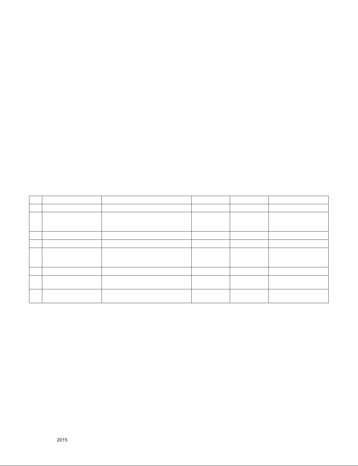
4. Electrical Specification
No Item Specication Measurement Result Remark
1 Receiving System 1) SBTVD / NTSC / PAL-M / PAL-N
2 Available Channel 1) VHF : 02~13
3 Input Voltage 1) AC 100 ~ 240V 50/60Hz
4 Market Central and South AMERICA
5 Aspect Ratio 16:9
2) UHF : 14~69
3) CATV : 01~135
6 Tuning System FS
7 Operating Environment 1) Temp : 0 ~ 40 deg
2) Humidity : ~ 80 %
8 Storage Environment 1) Temp : -20 ~ 60 deg
2) Humidity : ~ 85 %
Only for training and service purposes
- 6 -
LGE Internal Use OnlyCopyright © LG Electronics. Inc. All rights reserved.
Page 7
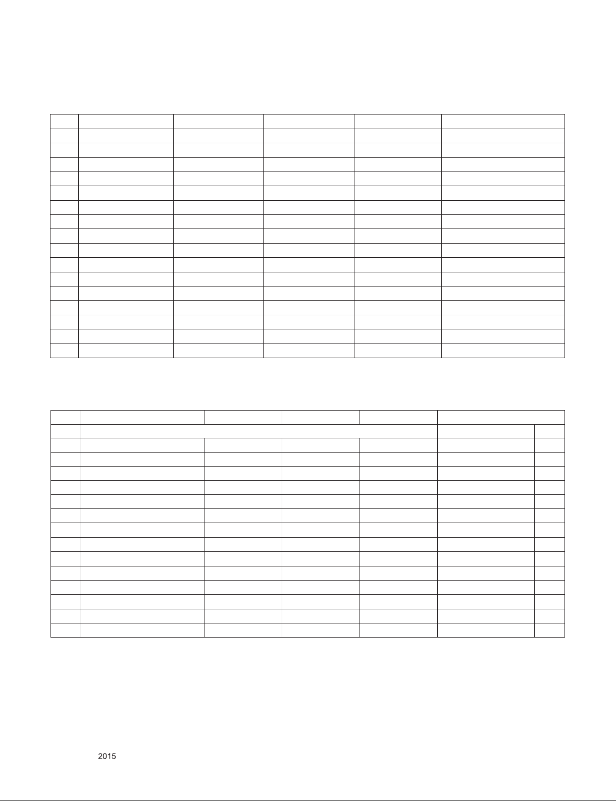
5. External Input Support Format
5.1. Component input(Y, CB/PB, CR/PR)
No Resolution H-freq(kHz) V-freq.(kHz) Pixel clock Proposed
1. 720*480 15.73 59.94 13.5 SDTV ,DVD 480I
2. 720*480 15.73 60 13.5135 SDTV ,DVD 480I
3. 720*480 31.47 59.94 27.0 SDTV 480P
4. 720*480 31.50 60 27.027 SDTV 480P
5. 1280*720 44.96 59.94 74.176 HDTV 720P
6. 1280*720 45.00 60.00 74.25 HDTV 720P
7. 1920*1080 28.12 50.00 74.250 HDTV 1080I
8. 1920*1080 33.72 59.94 74.176 HDTV 1080I
9. 1920*1080 33.75 60.00 74.25 HDTV 1080I
10. 1920*1080 26.97 23.976 74.176 HDTV 1080P
11. 1920*1080 27.00 24.000 74.25 HDTV 1080P
12. 1920*1080 33.71 29.97 74.176 HDTV 1080P
13. 1920*1080 33.75 30.000 74.25 HDTV 1080P
14. 1920*1080 56.25 50.00 148.50 HDTV 1080P
15. 1920*1080 67.43 59.939 148.352 HDTV 1080P
16. 1920*1080 67.50 60.00 148.50 HDTV 1080P
5.2. HDMI Input (PC/DTV)
*HDMI PC support only Rear HDMI Input
*If use DVI to HDMI cable for PC, you have to use external SPK for PC audio sound.
No Resolution H-freq(kHz) V-freq.(Hz) Pixel clock(MHz) Proposed
PC DDC
1
640*350 31.46 70.09 25.17 EGA X
2 720*400 31.46 70.08 28.32 DOS O
3 640*480 31.46 59.94 25.17 VESA(VGA) O
4 800*600 37.87 60.31 40.00 VESA(SVGA) O
5
1024*768 48.36 60.00 65.00 VESA(XGA) O
6
1152*864 54.34 60.053 80.00 VESA O
7
1360*768 47.71 60.015 85.50 VESA (WXGA) O
8
1280*1024 (FHD Only) 63.98 60.02 108.00 VESA (SXGA) O
9
1920*1080 (FHD Only) 67.5 60 148.5 HDTV 1080P O
10
3840 x 2160 (UF67 ONLY) 67.5 30.00 297.00
11
3840 x 2160 (UF67 ONLY) 56.25 25.00 297.00
12
3840 x 2160 (UF67 ONLY) 54.0 24.00 297.00
13
4096 x 2160 (UF67 ONLY) 53.95 23.97 296.703
14
4096 x 2160 (UF67 ONLY) 54 24.00 297.00
Only for training and service purposes
- 7 -
LGE Internal Use OnlyCopyright © LG Electronics. Inc. All rights reserved.
Page 8
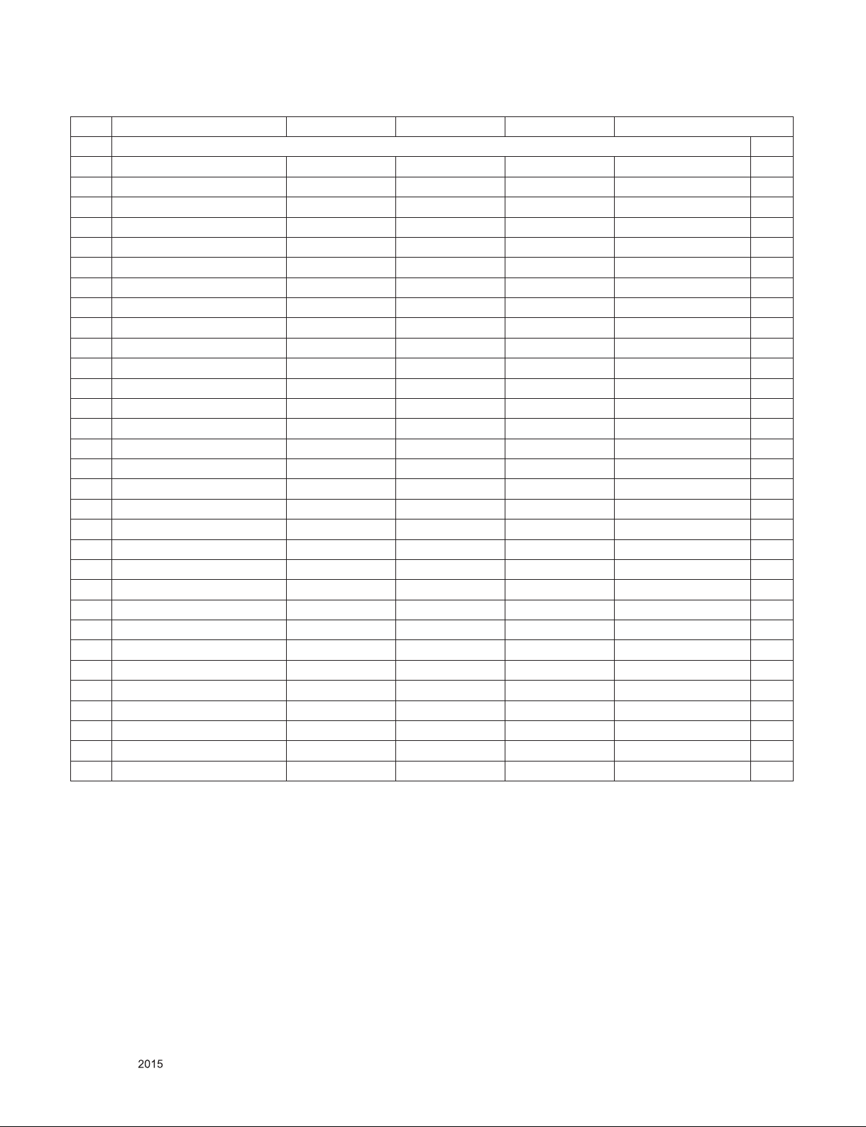
No Resolution H-freq(kHz) V-freq.(Hz) Pixel clock(MHz) Proposed
DTV
1
640 * 480 31.46 59.94 25.125 SDTV 480P
2
640 * 480 31.5 60.00 25.125 SDTV 480P
3
720*480 31.47 59.94 27.000 SDTV 480I
4
720*480 31.50 60.00 27.027 SDTV 480I
5
1280*720 37.50 50.00 74.25 HDTV 720P
6
1280*720 44.96 59.94 74.176 HDTV 720P
7
1280*720 45.00 60.00 74.25 HDTV 720P
8
1920*1080 28.12 50.00 74.25 HDTV 1080I
9
1920*1080 33.72 59.94 74.176 HDTV 1080I
10
1920*1080 33.75 60.00 74.25 HDTV 1080I
11
1920*1080 26.97 23.97 74.176 HDTV 1080P
12
1920*1080 27.00 24.00 74.25 HDTV 1080P
13
1920*1080 33.71 29.97 74.176 HDTV 1080P
14
1920*1080 33.75 30.00 74.25 HDTV 1080P
15
1920*1080 56.25 50.00 148.50 HDTV 1080P
16
1920*1080 67.43 59.94 148.352 HDTV 1080P
17
1920*1080 67.5 60.00 148.50 HDTV 1080P
18
3840 x 2160(UF67 ONLY) 53.95 23.98 UDTV 2160P
19
3840 x 2160(UF67 ONLY) 54 24.00 UDTV 2160P
20
3840 x 2160(UF67 ONLY) 56.25 25.00 UDTV 2160P
21
3840 x 2160(UF67 ONLY) 61.43 29.97 UDTV 2160P
22
3840 x 2160(UF67 ONLY) 67.5 30.00 UDTV 2160P
23
3840 x 2160(UF67 ONLY) 135 60.00 UDTV 2160P
24
3840 x 2160(UF67 ONLY) 135 59.94 UDTV 2160P
25
4096 x 2160(UF67 ONLY) 53.95 23.98 UDTV 2160P
26
4096 x 2160(UF67 ONLY) 54 24.00 UDTV 2160P
27
4096 x 2160(UF67 ONLY) 56.25 25.00 UDTV 2160P
28
4096 x 2160(UF67 ONLY) 61.43 29.97 UDTV 2160P
29
4096 x 2160(UF67 ONLY) 67.5 30.00 UDTV 2160P
30
4096 x 2160(UF67 ONLY) 135 60.00 UDTV 2160P
31
4096 x 2160(UF67 ONLY) 135 59.94 UDTV 2160P
* DTV Resolution #6 ~ #17 : Support dual play for 3D Models
※ HDMI Monitor Range Limits
Min Vertical Freq - 58 Hz
Max Vertical Freq - 62 Hz
Min Horiz. Freq - 30 kHz
Max Horiz. Freq - 83 kHz
Pixel Clock - 160 MHz
Only for training and service purposes
- 8 -
LGE Internal Use OnlyCopyright © LG Electronics. Inc. All rights reserved.
Page 9
ADJUSTMENT INSTRUCTION
1. Application
This spec sheet is applied all of the TV with LJ55A chassis.
2. Designation
1) The adjustment is according to the order which is
designated and which must be followed, according to the
plan whic al Unit: Product Specification Standard.
2) Power adjustment : Free Voltage.
3) Magnetic Field Condition: Nil.
4) Input signal Unit: Product Specification Standard.
5) Reserve after operation: Above 5 Minutes (Heat Run).
Temperature : at 25 ºC±5
Relative humidity : 65 ± 10%
Input voltage : 100~220V, 50/60Hz
6) Adjustment equipments : Color Analyzer (CA-210 or
CA-110), SVC remote controller
7) Push The “IN STOP KEY” – For memory initialization.
Case1 : Software version up
1) After downloading S/W by USB , TV set will reboot
automatically
2) Push “In-stop” key
3) Push “Power on” key
4) Function inspection
5) After function inspection, Push “In-stop” key.
ºC
3. Main PCB check process
* APC – After Manual-Insert, executing APC
* Boot file Download
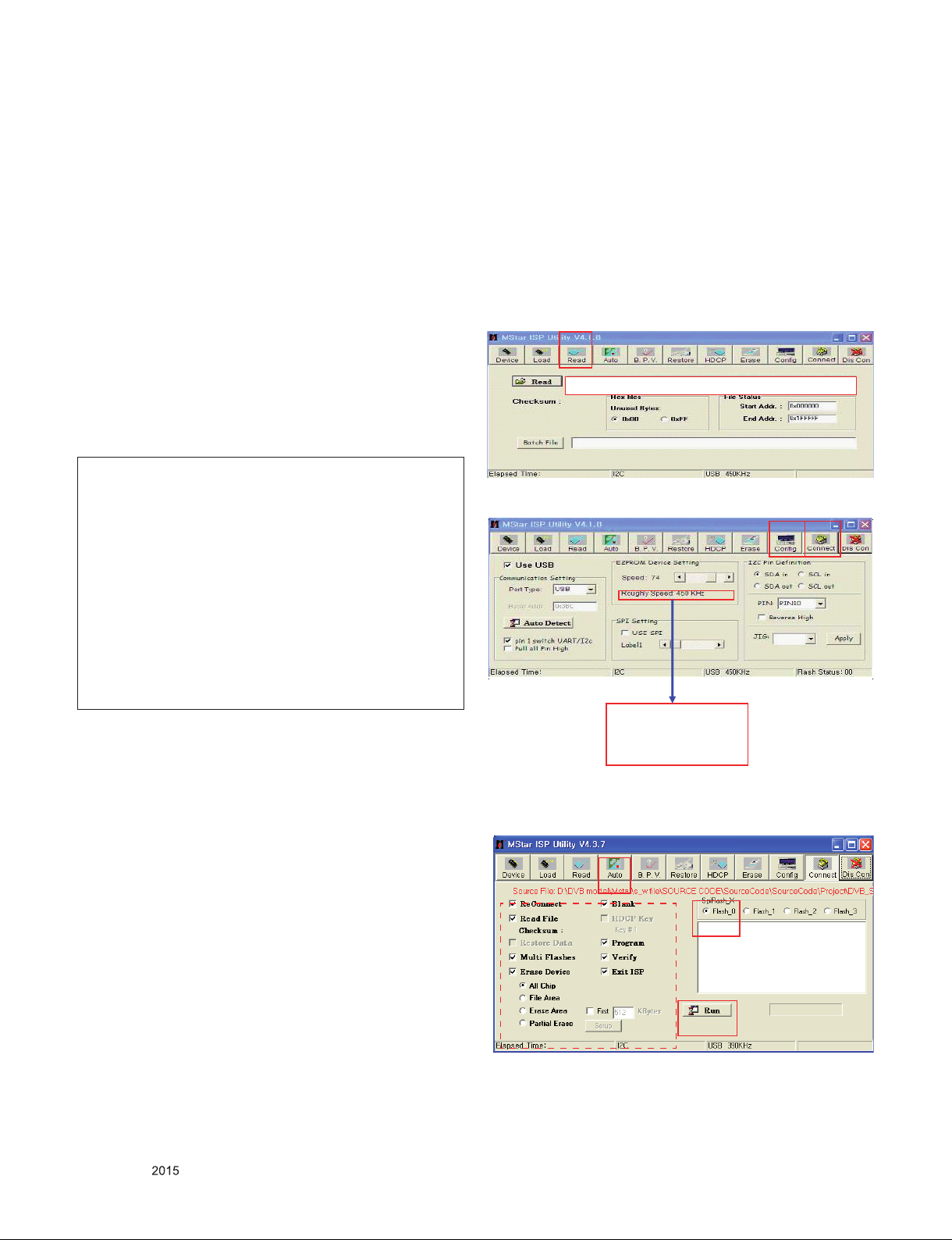
1) Execute ISP program “Mstar ISP Utility” and then click
“Config” tab.
2) Set as below, and then click “Auto Detect” and check “OK”
message.
If “Error” is displayed, Check connection between
computer, jig, and set.
3) Click “Read” tab, and then load download file (XXXX.bin) by
clicking “Read”
(1)
filexxx.bin
4) Click “Connect” tab. If “Can’t ” is displayed, Check
connection between computer, jig, and set.
(2)
(3)
Case2 : Function check at the assembly line
1) When TV set is entering on the assembly line, Push
“In-stop” key at first.
2) Push “Power on” key for turning it on.
→ If you push “Power on” key, TV set will recover channel
information by itself.
3).After function inspection, Push “In-stop” key.
Please Check the Speed
To use speed between
from 200KHz to 400KHz
5) Click “Auto” tab and set as below.
6) Click “Run”.
7) After downloading, check “OK” message.
(4)
filexxx.bin
(5)
(7)...........OK
(6)
Only for training and service purposes
- 9 -
LGE Internal Use OnlyCopyright © LG Electronics. Inc. All rights reserved.
Page 10
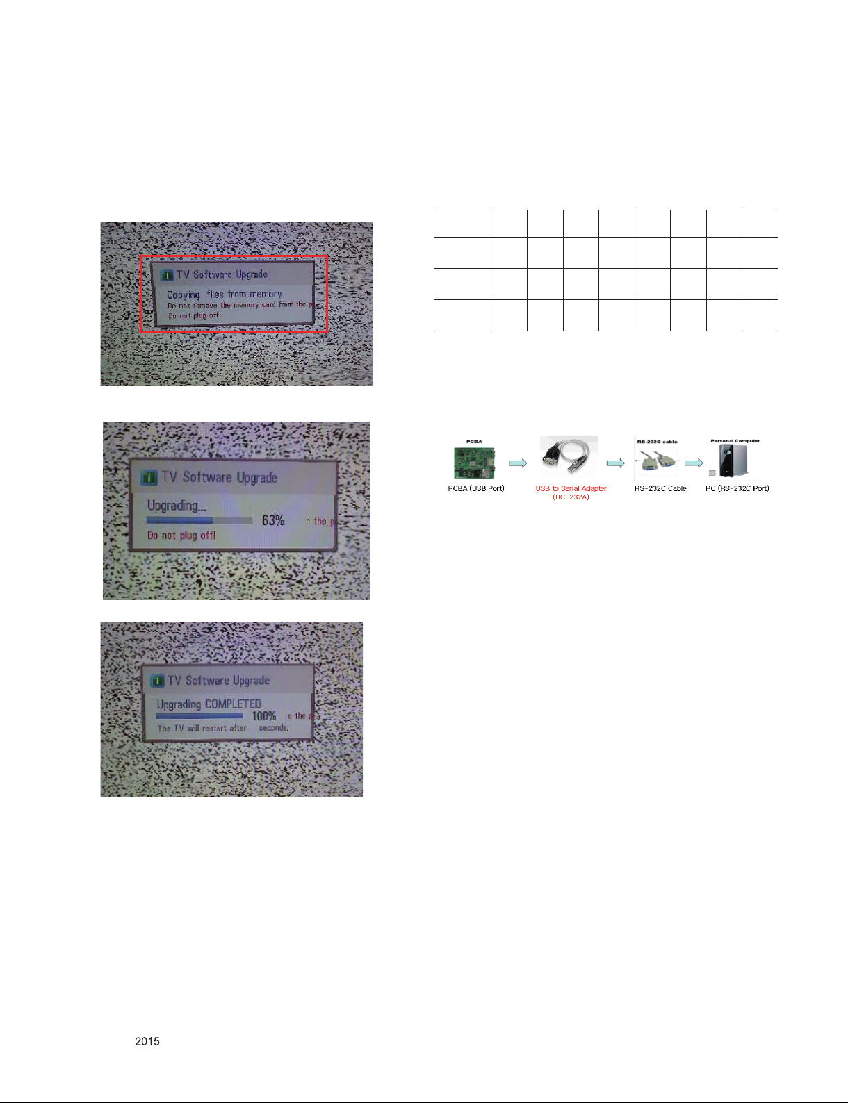
* USB DOWNLOAD(*.epk file download)
1) Put the USB Stick to the USB socket.
2) Automatically detecting update file in USB Stick.
- If your downloaded program version in USB Stick is Low,
it didn't work. But your downloaded version is High, USB
data is automatically detecting
3) Show the message "Copying files from memory"
4) Updating is staring.
* After downloading, have to adjust Tool
Option again.
1) Push "IN-START" key in service remote controller.
2) Select "Tool Option 1" and Push "OK" button.
3) Punch in the number. (Each model has their number.)
4) Completed selecting Tool option.
BLU
Tool
Tool
Tool
Tool
Tool
Model
32LF510B-
SB/D
43LF5100-
SA
49LF5100-
SA
Module
Type
option1
option2
option3
option4
LGD POLA 551 41899 4044 36384 9218
LGD POLA 556 33707 4044 36384 9218
LGD POLA 558 33707 4044 36384 9218
* RS-232C Connection Method
Connection : PCBA (USB Port) -> USB to Serial Adapter
(UC-232A) -> RS-232C cable -> PC(RS-232C port)
▪ Product name of USB to Serial Adapter is UC-232A.
※ Caution: LJ55H chassis support only UC-232A driver. (only
use this one. )
option5
Tool
option6
273
273
273
5) After updating is complete, The TV will restart automatically.
6) If TV turns on, check your updated version and Tool option.
(refer to the next page about tool option)
* If downloading version is higher than your TV have, TV
can lost all channel data. In this case, you have to
channel recover. If all channel data is cleared, you didn't
have a DTV/ATV test on production line.
Only for training and service purposes
- 10 -
LGE Internal Use OnlyCopyright © LG Electronics. Inc. All rights reserved.
Page 11
4. Total Assembly line process
4.1. Adjustment Preparation
■ W/B Equipment condition
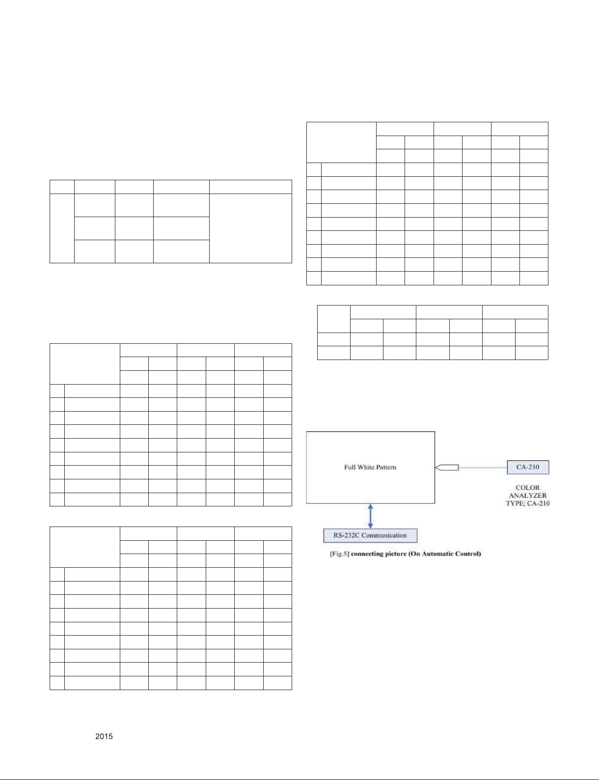
CA210 : CH14, Test signal : Inner pattern (80IRE) – in case of
LED back light
■ Above 5 minutes H/run in the inner pattern. (“power on” key of
adjust remote control)
► The spec of color temperature and coordinate
Model Mode Color Temp Color coordinate Remark
Cool (C50) 13,000k
Medium (0) 9,300k
All
Warm (W50) 6,500k
► CA210 : CH 14, Test signal : Inner pattern (80IRE)
- Standard color coordinate and temperature using CA-1000 (by
H/R time)
▪ L15 LGD, INX Module
March to December & Global
Normal line
H/R Time(Min)
271 270 286 289 313 329
1 0-2 282 289 297 308 324 348
2 3-5 281 287 296 306 323 346
3 6-9 279 284 294 303 321 343
4 10-19 277 280 292 299 319 339
5 20-35 275 277 290 296 317 336
6 36-49 274 274 289 293 316 333
7 50-79 273 272 288 291 315 331
8 80-119 272 271 287 290 314 330
9 Over 120 271 270 286 289 313 329
x = 0.271 (±0.002)
y = 0.270 (±0.002)
x = 0.286 (±0.002)
y = 0.289 (±0.002)
x = 0.313 (±0.002)
y = 0.329 (±0.002)
Cool Medium Warm
x y x x y x
※ Test signal
- Inner pattern for W/B adjust
- External white pattern
(80IRE, 204gray)
▪ Gumi Winter table(
January to February - Gumi production of prospective models all
models except Cinema Screen
Normal line
Cool Medium Warm
H/R Time(Min)
1 0-2 286 295 301 314 328 354
2 3-5 284 290 299 309 326 349
3 6-9 282 287 297 306 324 346
4 10-19 279 283 294 302 321 342
5 20-35 276 278 291 297 318 337
6 36-49 274 275 289 294 316 334
7 50-79 273 272 288 291 315 331
8 80-119 272 271 287 290 314 330
9 Over 120 271 270 286 289 313 329
▪
INX, AUO, Sharp, CSOT (13000K Cool the SPEC)
spec 271 270 286 289 313 329
target 278 280 293 299 320 339
x y x x y x
271 270 286 289 313 329
cool med warm
x y x y x y
※ Connecting picture of the measuring instrument
(On Automatic control)
Inside PATTERN is used when W/B is controlled. Connect to
auto controller or push Adjustment R/C POWER-ON -> Enter
the mode of White-Balance, the pattern will come out.
▪ Aging chamber line
Cool Medium Warm
H/R Time(Min)
1 0-5 280 285 294 308 319 340
2 6-10 276 280 290 303 315 335
3 11-20 272 275 286 298 311 330
4 21-30 269 272 283 295 308 327
5 31-40 267 268 281 291 306 323
6 41-50 266 265 280 288 305 320
7 51-80 265 263 279 286 304 318
8 81-119 264 261 278 284 303 316
9 Over 120 264 260 278 283 303 315
Only for training and service purposes
x y x x y x
271 270 285 293 313 329
● Auto-control interface and directions
1) Adjust in the place where the influx of light like floodlight
around is blocked. (Illumination is less than 10ux).
2) Adhere closely the Color Analyzer ( CA210 ) to the module
less than 10cm distance, keep it with the surface of the
Module and Color Analyzer’s Prove vertically.(80~100°).
3) Aging time
- After aging start, keep the power on (no suspension of
power supply) and heat-run over 5 minutes.
- Using ‘no signal’ or ‘full white pattern’ or the others, check
the back light on.
- 11 -
LGE Internal Use OnlyCopyright © LG Electronics. Inc. All rights reserved.
Page 12
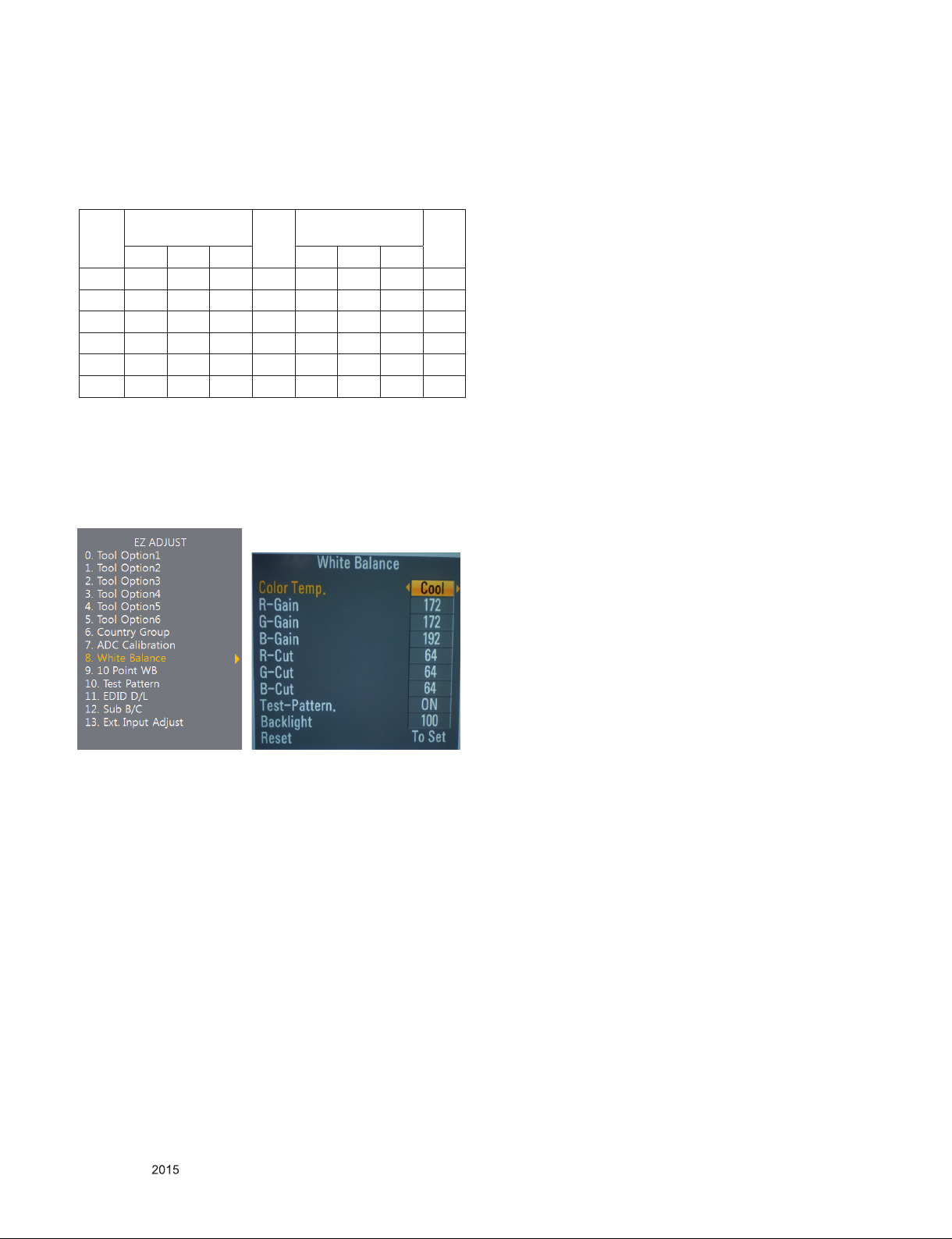
● Auto adjustment Map(RS-232C)
RS-232C COMMAND
[ CMD ID DATA ]
Wb 00 00 White Balance Start
Wb 00 ff White Balance End
RS-232C COMMAND
[CMD ID DATA]
Cool Mid Warm Cool Mid Warm
R Gain jg Ja jd 00 172 192 192 192
G Gain jh Jb je 00 172 192 192 192
B Gain ji Jc jf 00 192 192 172 192
R Cut 64 64 64 128
G Cut 64 64 64 128
B Cut 64 64 64 128
MIN
CENTER
(DEFAULT)
MAX
*Manual W/B process using adjusts Remote control.(TBD)
■ Color analyzer(CA100+, CA210) should be used in the
calibrated ch by CS-1000
■ Operate the zero-calibration of the CA100+ or CA-210, then
stick sensor to the module when adjusting.
■ After enter Service Mode by pushing “ADJ” key,
■Enter White Balance by pushing “►” key at “8. White Balance”.
5) Adjust two modes (Medium / Warm) Fix the one of R/G/B gain
to 192 (default data) and decrease the others.
6) Adj. is completed, Exit adjust mode using “EXIT” key on
Remote controller.
▪ If internal pattern is not available, use RF input. In EZ Adj. menu
8. White Balance, you can select one of 2 Test-pattern: ON,
OFF. Default is inner (ON). By selecting OFF, you can adjust
using RF signal in 206 Gray pattern.
※ CASE Cool
First adjust the coordinate far away from the target value(x, y).
1) x, y > target
i) Decrease the R, G.
2) x, y < target
i) First decrease the B gain,
ii) Decrease the one of the others.
3) x > target , y< target
i) First decrease B, so make y a little more than the target.
ii) Adjust x value by decreasing the R
4) x < target , y >target
i) First decrease B, so make x a little more than the target.
ii) Adjust x value by decreasing the G
How to adjust
1) If G gain is adjusted over 172 and R gain and B gain less
than 192 , Adjust is O.K.
2) If G gain is less than 172 , increase G gain by up to 172, and
then increase R gain and B gain same amount of increasing
G gain.
3) If R gain or B gain is over 255 , Readjust G gain less than
172, Conform to R gain is 255 or B gain is 255
■ For manual adjustment, it is also possible by the following
sequence.
1) Set TV in Adj. mode using POWER ON
2) Zero Calibrate the probe of Color Analyzer, then place it on the
center of LCD module within 10cm of the surface
3) Press ADJ key -> EZ adjust using adj. R/C -> 8. White-Balance
then press the cursor to the right (KEY►). When KEY(►) is
pressed 206 Gray internal pattern will be displayed.
4) Adjust Cool modes
(i). Fix the one of R/G/B gain to 192 (default data) and
decrease the others
(If G gain is adjusted over 172 and R and B gain less than
192, increase G gain to 192 and increase R gain and B gain
same amount of increasing G gain.)
(ii). If G gain is less than 172,
Increase G gain by up to 172, and then increase R gain and
G gain same amount of increasing G gain.
(iii). If R gain or B gain is over 255,
Readjust G gain less than 172, Conform to R gain is 255 or
B gain is 255
※ CASE Medium / Warm
First adjust the coordinate far away from the target value(x, y).
1) x, y > target
i) Decrease the R, G.
2) x, y < target
i) First decrease the B gain,
ii) Decrease the one of the others.
3) x > target , y< target
i) First decrease B, so make y a little more than the target.
ii) Adjust x value by decreasing the R
4) x < target , y >target
i) First decrease B, so make x a little more than the target.
ii) Adjust x value by decreasing the G
▪ After You finish all adjustments, Press “In-start” button and
compare Tool option and Area option value with its BOM, if it is
correctly same then unplug the AC cable. If it is not same, then
correct it same with BOM and unplug AC cable. For correct it to
the model’s module from factory JIG model.
▪ Push the “IN STOP KEY” after completing the function
inspection.
Only for training and service purposes
- 12 -
LGE Internal Use OnlyCopyright © LG Electronics. Inc. All rights reserved.
Page 13
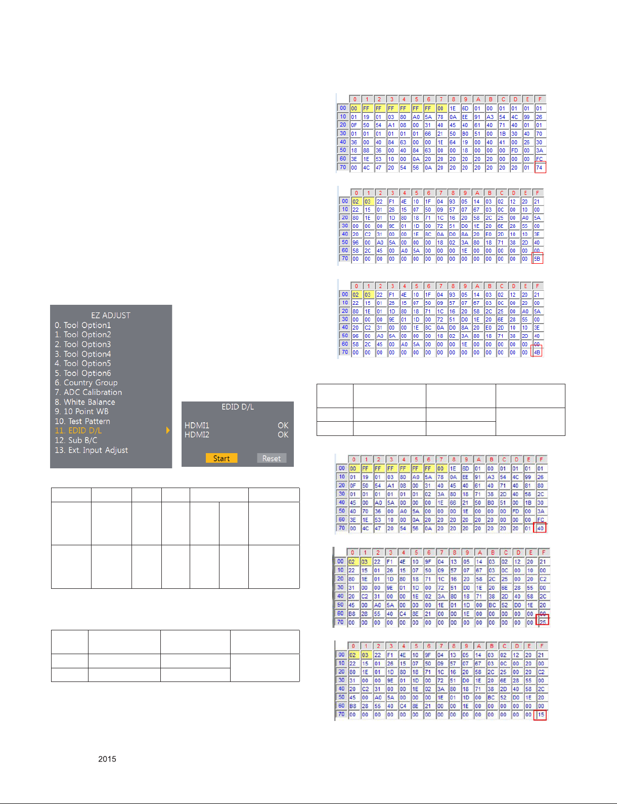
4.2. DPM operation confirmation
(Only Apply for MNT Model)
Check if Power LED Color and Power Consumption operate
as standard.
■ Set Input to RGB and connect D-sub cable to set
■ Measurement Condition: (100~240V@ 50/60Hz)
■ Confirm DPM operation at the state of screen without Signal
- HDMI1/2 (128)
4.3. EDID DATA
1) All Data : HEXA Value
2) Changeable Data :
*: Serial No : Controlled / Data:01
**: Month : Controlled / Data:00
***:Year : Controlled
****:Check sum
- Auto Download
■ After enter Service Mode by pushing “ADJ” key,
■ Enter EDID D/L mode.
■ Enter “START” by pushing “OK” key.
- HDMI1 (256)
- HDMI2 (256)
2) FHD 2D EDID Data (S/W 1.01.20)
CheckSum
(0xFF)
HDMI 1 40 / 25 10
HDMI 2 40 / 15 20
Physical Address
- HDMI1/2 (128)
(0x1E)
Remark
※ Edid data and Model option download (RS232C)
NO Item CMD 1 CMD 2 Data 0
Enter
download
MODE
Edid data
and Model
option
download
Download
‘Mode In’
Download A E 00 10
A A 0 0
When transfer
the ‘Mode In’,
Carry the command
Automatically
download
(The use of a
internal Data)
● EDID DATA
1) HD 2D EDID Data
Before S/W version
CheckSum
(0xFF)
HDMI 1 74 / 5B 10 LF51 has Only
HDMI 2 74 / 4B 20
Only for training and service purposes
Physical Address
(0x1E)
Remark
HDMI1
- 13 -
- HDMI1 (256)
- HDMI2 (256)
LGE Internal Use OnlyCopyright © LG Electronics. Inc. All rights reserved.
Page 14

4.4. Outgoing condition Configuration
■ When pressing IN-STOP key by SVC remocon, Red LED
are blinked alternatively. And then automatically turn off.
(Must not AC power OFF during blinking)
4.5. GND & Hi-pot test
4.5.1. GND & HI-POT auto-check preparation
1) Check the POWER CABLE and SIGNAL CABE insertion
condition
4.5.2. GND & HI-POT auto-check
1) Pallet moves in the station. (POWER CORD / AV CORD is
tightly inserted)
2) Connect the AV JACK Tester.
3) Controller (GWS103-4) on.
4) GND Test (Auto)
- If Test is failed, Buzzer operates.
- If Test is passed, execute next process (Hi-pot test).
(Remove A/V CORD from A/V JACK BOX)
5) HI-POT test (Auto)
- If Test is failed, Buzzer operates.
- If Test is passed, GOOD Lamp on and move to next
process automatically.
4.5.3. Checkpoint
1) Test voltage
① 3 Poles
- GND: 1.5KV/min at 100mA
- SIGNAL: 3KV/min at 100mA
② 2 Poles
- SIGNAL: 3KV/min at 100mA
2) TEST time: 1 second
3) TEST POINT
① 3 Poles
- GND Test = POWER CORD GND and SIGNAL CABLE
GND.
- Hi-pot Test = POWER CORD GND and LIVE &
NEUTRAL.
② 2 Poles
- Hi-pot Test = Accessible Metal and LIVE & NEUTRAL.
4) LEAKAGE CURRENT: At 0.5mArms
Only for training and service purposes
- 14 -
LGE Internal Use OnlyCopyright © LG Electronics. Inc. All rights reserved.
Page 15
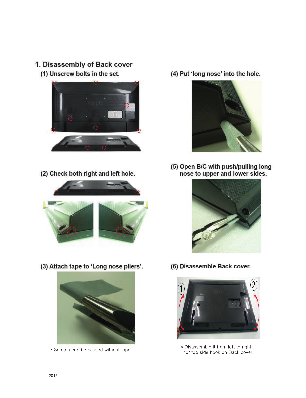
DISASSEMBLY
Only for training and service purposes
- 15 -
LGE Internal Use OnlyCopyright © LG Electronics. Inc. All rights reserved.
Page 16
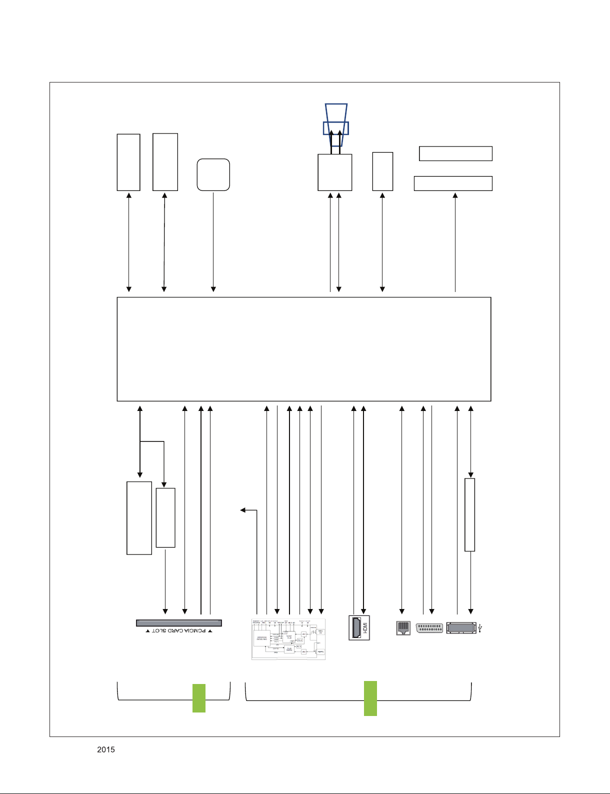
BLOCK DIAGRAM
Serial Flash
SPI_SCK/SDI/SDO/CS
System EEPROM
I2C_SCL/SDA
SPK_L
SPK_R
30P HD LVDS wafer
(P1801)
HZ
24M
X- tal
NTP7515
AUD_LRCH,
AMP_SCL/SDA
AUD_MASTER_CLK,
AUD_LRCK, AUD_SCK
Connector
(P1800)
Jog KEY, LED_R, IR
RXACK+/-
RXB0+/- ~RXB4+/-,
RXA0+/-~RXA4+/-,
51P FHD LVDS wafer
-
RXBCK+/
Main SOC
M1A-LGE2136
(IC101, DDR3 256MB)
PCM_A[0:7]
IC102 (1Gbit)
NAND FLASH
H27U1G8F2CTR-BC
T4LCX244FT Buffer
CI SLOT
PCM_A[8:14]
TS_DATA[0:7]
PCM_DATA[0:7]
SIDE
IF_N/P
LNB_TX
LNB_OUT, DEMOD_RESET
FE_TS_DATA[0:7]
TU_SCL / SDA
DEMOD_SCL/SDA
Tuner
F/NIM
IF_AGC
EPHY_TP/TN/RP/RN
DDC_SCL/SDA_2, HDMI_CEC
CK+/-, D0+/ -, D1+/ -, D2+/ -_HDMI2
HDMI1
LAN
Only UK
REAR
USB1_OCP/CTL
OCP
DM/DP
SN1406035RGER
SC1/AV2_CVBS_IN, SC1_R+/G+/B+
DTV/MNT_OUT, DTV/MNT_L/R_OUT
+5V_USB
F- SCART
USB
Only for training and service purposes
- 16 -
LGE Internal Use OnlyCopyright © LG Electronics. Inc. All rights reserved.
Page 17
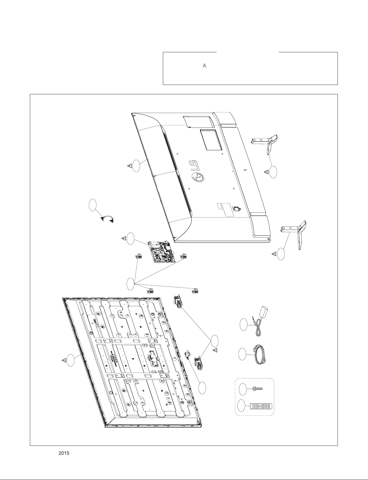
EXPLODED VIEW
IMPORTANT SAFETY NOTICE
Many electrical and mechanical parts in this chassis have special safety-related characteristics. These
parts are identified by in the Schematic Diagram and EXPLODED VIEW.
It is essential that these special safety parts should be replaced with the same components as
recommended in this manual to prevent Shock, Fire, or other Hazards.
Do not modify the original design without permission of manufacturer.
400
900
LV1
200
540
800
500
120
700
A10
A2
901
701
Set + Stand
Only for training and service purposes
- 17 -
LGE Internal Use OnlyCopyright © LG Electronics. Inc. All rights reserved.
Page 18
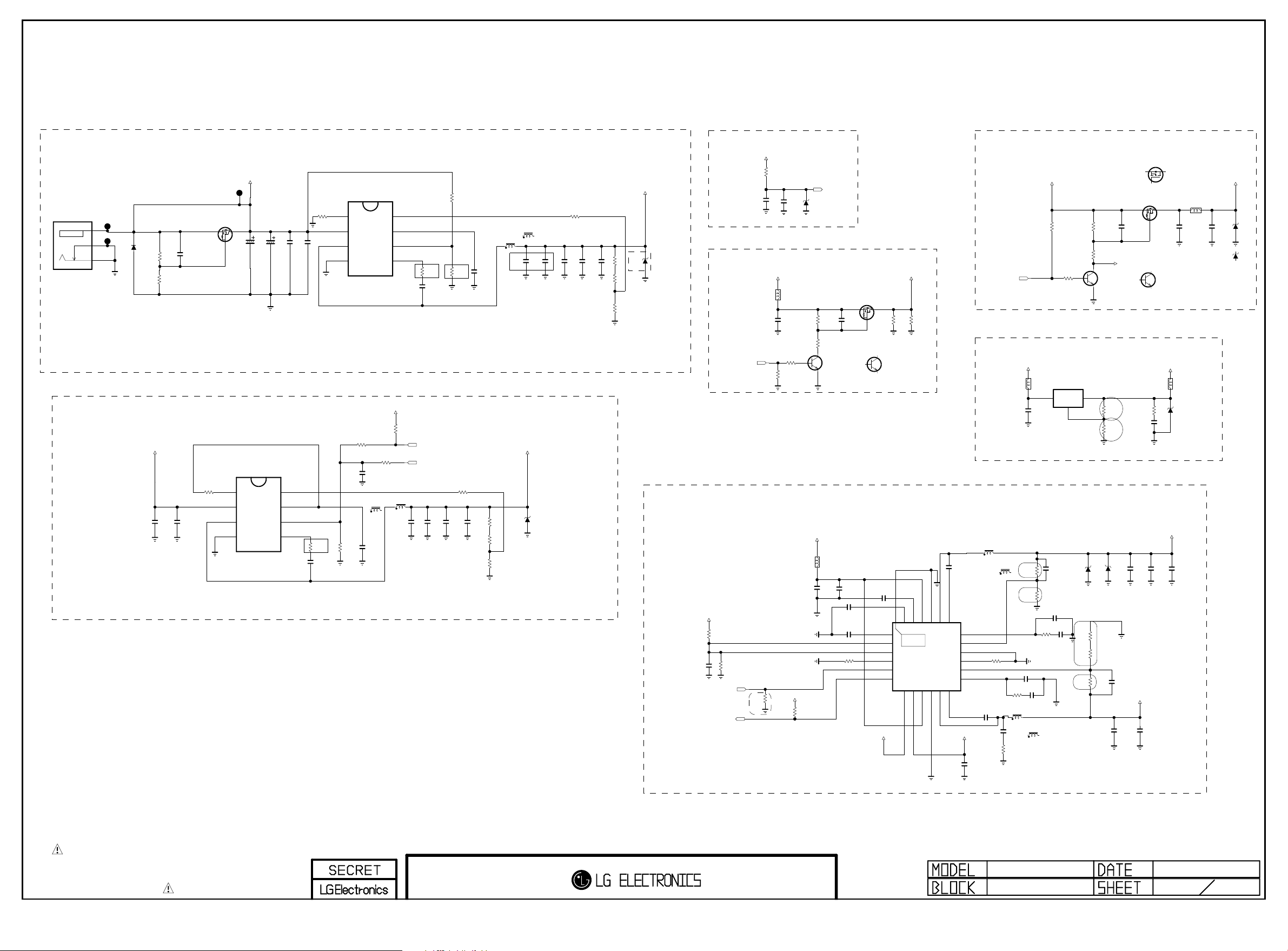
POWER
Copyright ⓒ 2015 LG Electronics. Inc. All right reserved.
Only for training and service purposes
LGE Internal Use Only
FROM ADAPTOR 19V
JK400
KJA-DC-1-0032
4
4
2
Surge Protection
2
1
1
D471
20V
OPT
R493
120K
OPT
R492
120K
OPT
C492
10uF
25V
19V TO PANEL VCC(12V) DCDC CONVERTER
+19V
C472
C470
10uF
0.1uF
25V
25V
R470
100K
OPT
Q407
SSM3J332R
S
G
AAM
IN
SW
GND
+19V
D
MP2315GJ
1
2
3
4
OPT
C488
68uF
35V
IC403
NEW
3A
+19V to +3.5V_STANDBY
IC402
MP2315GJ
R471
AAM
C471
68uF
35V
8
7
6
5
C473
10uF
FB
VCC
EN/SYNC
BST
25V
39K
1/16W
1%
C474
0.1uF
25V
20130528 cJ.LIM
R475
68
C475
0.1uF
50V
GND
IN
SW
0.47uF
OPT
R476
47K
OPT
C477
1
2
NEW
3
3A
4
OPT
R489
10K
16V
CYNTEC
L470-*1
10uH
C478
0.1uF
25V
FB
8
VCC
7
EN/SYNC
6
BST
5
+3.5V_ST
OPT
R490
10K
R480
10K
TDK
L470
10uH
C480
10uF
20130528 cJ.LIM
C481
10uF
16V
16V
R478
100K
R479
R477
68
20K
C476
0.1uF
50V
RL_ON
POWER_ON/OFF_1
C483
C486
0.1uF
10uF
25V
16V
R481
56K
R48 2
R48 3
3.3 K
R48 4
C479
0.1uF
25V
11K
1%
1%
1K
1%
CYNTEC
L471-*1
4.7uH
TDK
L471
4.7uH
C482
C484
10uF
10uF
10V
10V
X5R => X7R
To improve CST Issue
2013.12.21 by GH.Song
+12V
OPT
ZD405
15V
C487
22uF
10V
R485
56K
C489
22uF
10V
C485
0.1uF
25V
R48 6
R48 7
1.2 K
R48 8
3.5V_ST POWER_DET
+3.5V_ST
R410
10K
+3.5V_ST
C400
0.1uF
16V
2K
1%
1%
1K
1%
5V
5.6B->5V
READY->APPLY
2013.08.07
D470
+12V to PANEL_VCC
UBW2012-121F
PANEL_CTL
L408
120OHM
OPT
C425
0.1uF
25V
R441
OPT
C490
1uF
10V
+12V
R442
10K
10K
B
R445
R446
120K
OPT
ZD408
33K
5V
C
E
POWER_DET
C427
0.22uF
25V
TR_NXP
Q403
MMBT3904(NXP)
Q405
SSM3J332R
S
B
PANEL_VCC
D
R451
R452
5.6K
5.6K
G
C
TR_KEC
Q403-*1
2N3904S
E
+3.5V_ST to +3.3V_Normal
+3.5V_ST
POWER_ON/OFF_1
R443
4.7K
R444
10K
B
R447
22K
R448
2.2K
C428
2.2uF
10V
C
TR_NXP
Q404
MMBT3904(NXP)
E
+3.5V_Normal to +1.5V_DDR
+3.3V_Normal
L409
BLM18PG121SN1D
C426
10uF
10V
1.3A
IC404
AZ1117EH-ADJTRG1
OUTIN
ADJ/GND
R449
1K
1/16W
1%
R450
200
1/16W
1%
BOOST_EN
R1
R2
FET_AOS
Q406-*1
AO3435
S
G
FET_TOSHIBA
Q406
SSM3J332R
S
G
C
B
E
L411
CB2012PK501T
R453
0
C431
10uF
10V
D
D
C429
0.1uF
16V
TR_KEC
Q404-*1
2N3904S
+1.5V_DDR
L410
BLM18PG121SN1D
C430
22uF
10V
BRAZIL_ESD
ZD403
2.5V
+3.3V_Normal
TVS_SEMTECH
ZD402
5V
TVS_KEC
ZD402-*1
Vout=1.25*(1+R2/R1)+Iadj*R2
+5V_Normal & +1.10V_VDDC
+3.3V_Normal
R403
10K
OPT
C403
4700pF
50V
USB1_CTL
Check the pull down
when AC Power On with HDD
USB1_CTL_Pull_Down
USB1_OCD
OPT
R473
30K
R472
3.3K
CB2012PK501T
+5V_Normal
R408
100K
L404
+12V
C405
10uF
25V
Vout=0.6(R1/R2)+0.6
TDK
L405
4.7uH
CYNTEC
R1
R411
4.7K
1%
R2
R413
5.1K
1%
50V
C420
3300pF
50V
CYNTEC
L406-*1
4.7uH
R41 4
OPT
OPT
C411
ZD407
82pF
5.1v
50V
C416
22pF
50V
C417
3300pF
50V
10K
R415
R416
5.1K
R417
100
1%
1%
39K
1%
ZD401
2.5V
R1
R2
C412
10uF
6.3V
C418
47pF
50V
+5V_Normal
C423
22uF
16V
C410
0.047uF
25V
C406
10uF
25V
C408
OPT
2200pF
50V
C409
OPT
2200pF
50V
R409
91K
C407
1uF
10V
SS2
EN1
EN2
ROSC/SYNC
SW_EN
NFAULT
+5V_USB
VIN123V7V24SS1
[EP]
22
1
THERMAL
25
2
3
IC400
SN1406035RGER
4
5
6
7
9
8
VIN2
SW_IN
SW_OUT
10
PGND2
LX2
BST120LX121PGND1
19
COMP1
18
FB1
17
AGND
16
RSET
15
FB2
14
COMP2
13
11
12
BST2
+5V_Normal
C432
1uF
16V
L405-*1
4.7uH
R422
15K
C419 22pF
R41 8
20K
TDK
C421
0.047uF
L406
4.7uH
25V
C491
470pF
50V
R491
5.1
Vout=0.6(R1/R2)+0.6
C413
22uF
10V
C424
22uF
16V
+1.10V_VDDC
C414
22uF
10V
THE SYMBOL MARK OF THIS SCHEMETIC DIAGRAM INCORPORATES
SPECIAL FEATURES IMPORTANT FOR PROTECTION FROM X-RADIATION.
FIRE AND ELECTRICAL SHOCK HAZARDS, WHEN SERVICING IF IS
ESSENTIAL THAT ONLY MANUFACTURES SPECIFIED PARTS BE USED FOR
THE CRITICAL COMPONENTS IN THE SYMBOL MARK OF THE SCHEMETIC.
L15.5_ECI_M1A
POWER
150112
4
Page 19
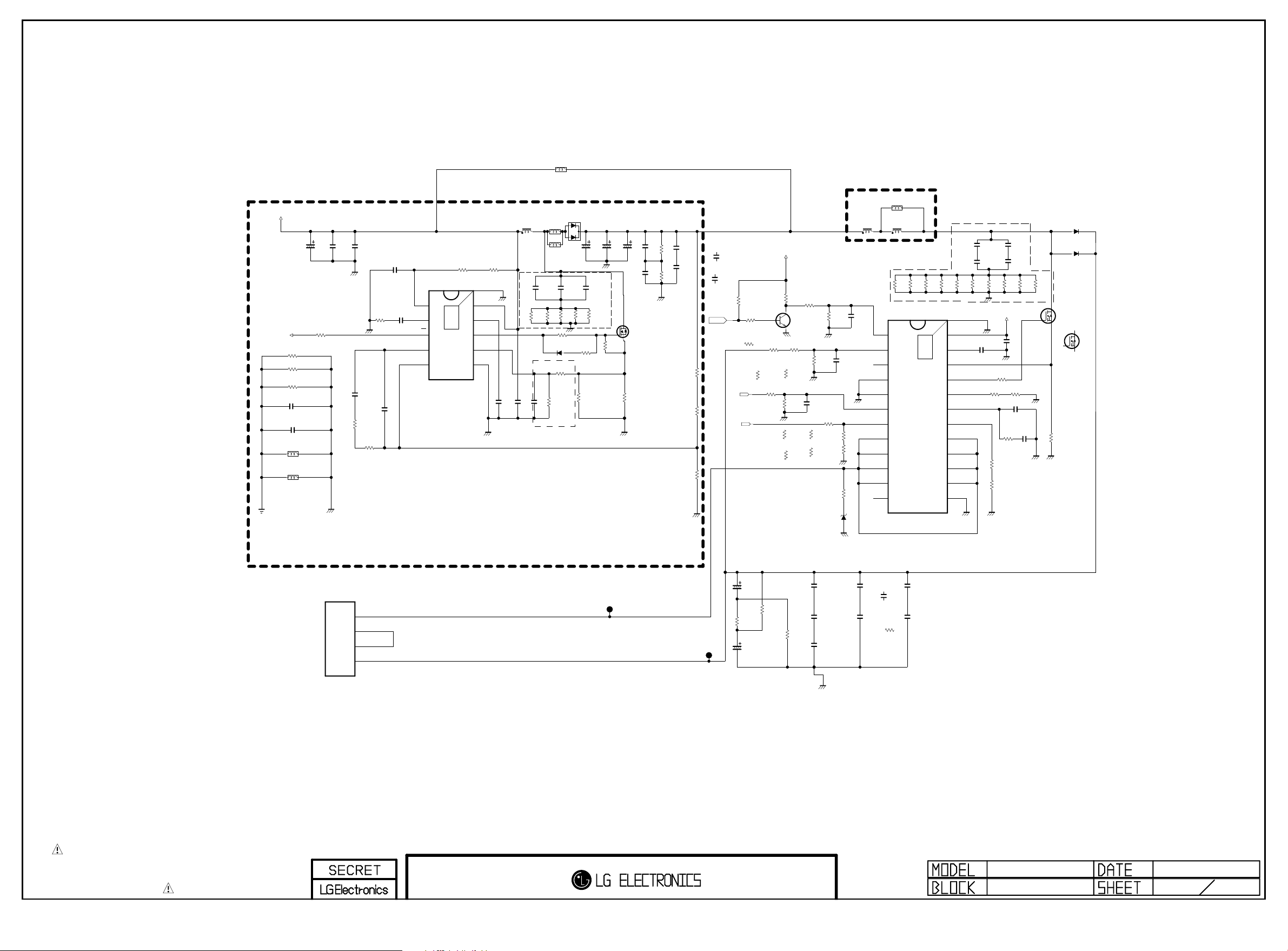
TOTAL LED DRIVER BLOCK
Copyright ⓒ 2015 LG Electronics. Inc. All right reserved.
Only for training and service purposes
LGE Internal Use Only
L505
CIS21J121
32_43inch
+19V
BOOST_EN
EU_BR
R553
0
R554
0
32_43inch_AJ_KR_CO
R555
0
OPT
C516
0.1uF
OPT
C517
0.1uF
OPT
L503
UBW2012-121F
OPT
L504
UBW2012-121F
C500
47uF
25V
49inch
R500
1K
C501
10uF
25V
C502
0.1uF
50V
OPT
49inch
C503
0.033uF
50V
49inch
R501
18K
1%
49inch
470pF
49inch
R502
1K
1%
49inch
R503
10K
1/16W
C504
50V
49inch
C505
100pF
50V
49inch
C506
0.22uF
REDUCE INDUCTOR TEMP ISSUE
49inch
49inch
L507
49inch
L508
49inch
C531
100V
220pF
R511
R508
47
49inch
49inch
R509
49inch
3.3
OPT
D505
1N4148W-G
49inch
R510
3.9K
49inch
50V
R507
3.9K
1%
121211
1K -> 3.9K
220p -> 330p
D503
MBRD10U100CT
A1
C
A2
OPT
C532
100V
220pF
47
R513
47
49inch
49inch
R582
2.2
1%
49inch
R558
47
OPT
R512
49inch
C511
33uF
100V
0.1
OPT
R583
10K
1W
REDUCE RIPPLE CURRENT
49inch
49inch
C513
C512
33uF
33uF
100V
100V
D
49inch
Q500
G
AOD478
S
R514
0.1
49inch
1W
49inch
C514
1uF
50V
49inch
C515
1uF
50V
49inch
32_43inch_AJ_KR_CO
R515
C537
100K
4.7uF
1/8W
50V
32_43inch_AJ_KR_CO
C538
49inch
4.7uF
R516
50V
100K
1/8W
R518
47K
49inch
R581
1K
49inch
49inch
R517
680
1/8W
1%
VOUT#1=50.5V
49inch
C537-*1
10uF
35V
49inch
C538-*1
10uF
35V
OPT
R519
10K
INV_CTL
PWM_DIM
R520
10K
B
49inch
R522-*1
32_43inch
150K
R522
120K
43inch
R529-*1
13K
1%
R521
100
BLU_CURRENT_CTL
+3.3V_Normal
R523
3K
C
TR501
MMBT3904(NXP)
E
R525
270K
1/8W
1%
49inch
R529-*2
8.2K
1%
R524
100K
49inch
R532-*2
27K
1%
49inch
1%
R533-*2
3.3K
1/16W
R528
1K
1%
32inch
R529
30K
1%
C518
100pF
50V
43inch
R532-*1
12K
1%
43inch
R533-*1
10K
1%
OPT
R530
100K
R531
100K
1%
10K
C521
1000pF
50V
32inch
R532
32inch
R533
15K
1%
3.6K
1%
C522
1000pF
50V
R534
49inch
L500
33uH
49inch
49inch
R504
R505
180K
180K
49inch
C507
1uF
25V
To Improve EMI Issue
49inch
C530
100V
220pF
R506
47
49inch
49inch
49inch
C509
C508
0.1uF
330pF
50V
VOUT = VREF*(1+48.8K/680)
= 0.7 *(1+48.8K/680)
= 50.5V
49inch
IC500
TPS40210DGQR
RC
1
SS
DIS/EN
COMP
2
3
4
FB
5
16V
11
THERMAL
[EP]
VDD
10
BP
9
GDRV
8
ISNS
7
GND
6
L501
33uH
NC_1
PGND_1
PGND_2
PDIM
RISET
NC_2
EN
OVP
LS8
LS7
LS6
LS5
32inch
L506
CIS21J121
43_49inch
L502
33uH
R535
100
DT1641AS
1
2
3
4
5
6
7
8
9
10
11
12
R536
100
IC501
To Improve EMI Issue
C523
100V
220pF
C524
100V
220pF
R537
R538
R539
100
100
100
[EP]GND
VIN
24
C525 1uF
VREF
25
23
THERMAL
CS
22
NDRV
21
RSS
20
COMP
19
RT
18
LS1
17
LS2
16
LS3
15
LS4
14
LGND
13
R540
100
25V
220K
R545
R541
100
R542
R544
3.3
1/16W
39K
1%
R543
1.5K
1%
+19V
1%
R546
1.5K 1%
C526
100V
220pF
C527
100V
220pF
R547
100
C510
1uF
25V
R548
30K
C528
4700pF
50V
1%
C529
0.1uF
R549
100
25V
UF3D(SUZHOU GRANDE)
32_43inch
R550
100
D
49inch
Q502
SMN630LD
G
32_43inch
S
Q502-*1
G
AOD2922
R551
0.1
49inch
D502
D504
BR210
100V
D
S
P500
SMAW200-04
FIRST BOOST UP
1
2
3
VOUT#2
4
EXCEPT C500 C501
C533
33uF
49inch
R579
0
C534
33uF
32_43inch
R580
0
32_43inch
R578
0
C535
4.7uF
50V
C536
4.7uF
50V
C539
4.7uF
50V
33V
ZD500
43_49inch
C519
1uF
100V
49inch
C520
1uF
100V
32inch
C519-*1
4.7uF
50V
32_43inch
C520-*1
0
1/4W
5%
49inch
C540
1uF
100V
49inch
C541
1uF
100V
THE SYMBOL MARK OF THIS SCHEMETIC DIAGRAM INCORPORATES
SPECIAL FEATURES IMPORTANT FOR PROTECTION FROM X-RADIATION.
FIRE AND ELECTRICAL SHOCK HAZARDS, WHEN SERVICING IF IS
ESSENTIAL THAT ONLY MANUFACTURES SPECIFIED PARTS BE USED FOR
THE CRITICAL COMPONENTS IN THE SYMBOL MARK OF THE SCHEMETIC.
LED_DRIVER
150112L15.5_ECI_M1A
5
Page 20
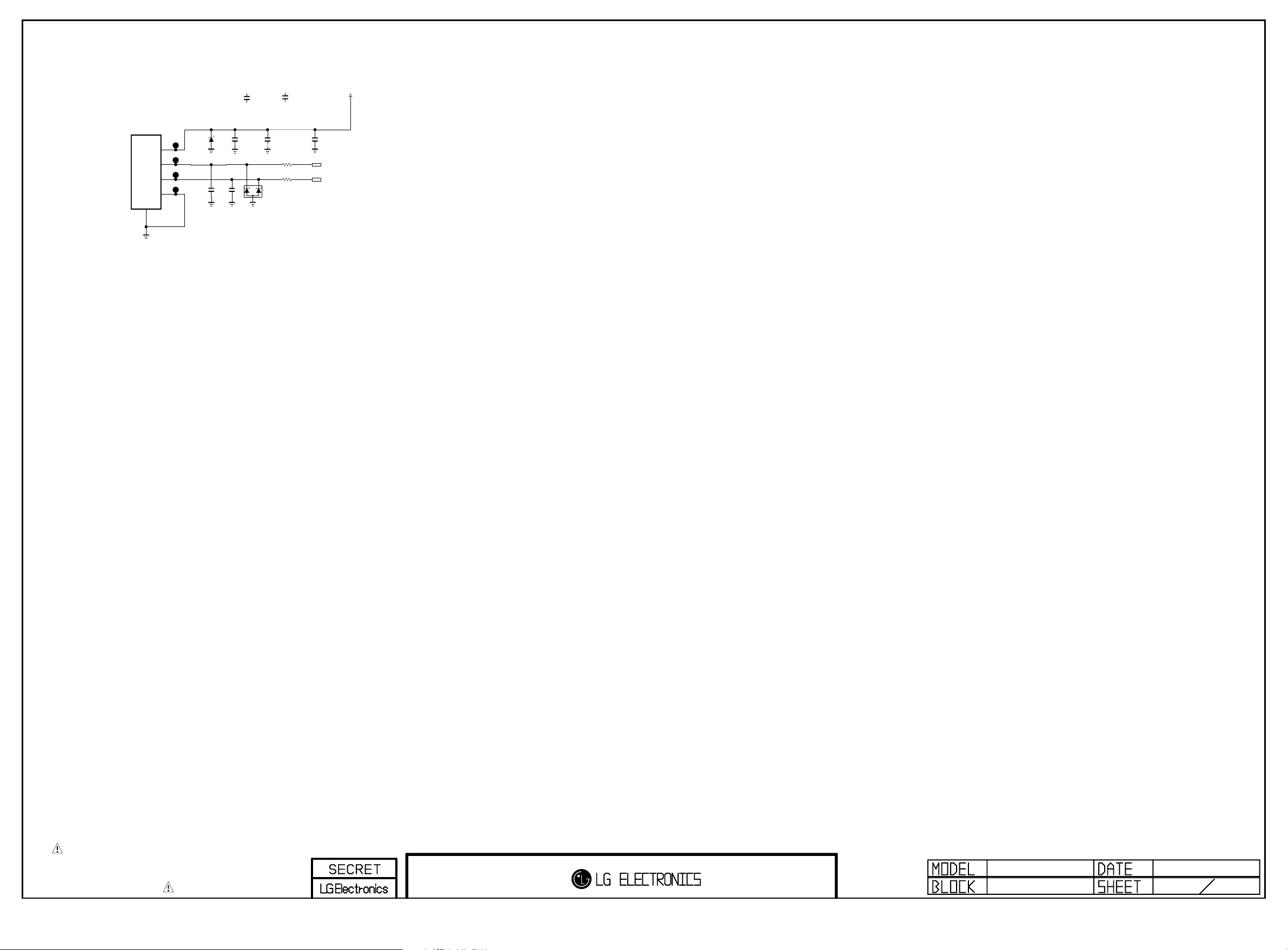
USB
Copyright ⓒ 2015 LG Electronics. Inc. All right reserved.
Only for training and service purposes
LGE Internal Use Only
JK700
US-04A-VSD
5
OPT
C704
22uF
10V
+5V_USB
SIDE_USB1_DM
SIDE_USB1_DP
USB_HDD_CAP1_10uF
C700-*1
USB_HDD_CAP1_22uF
OPT
ZD700
SD05
1
2
3
4
5V
C701
OPT
OPT
C702
5pF
5pF
50V
50V
10uF
10V
C700
22uF
10V
USB_HDD_CAP2_10uF
C703-*1
10uF
10V
USB_HDD_CAP2_22uF
C703
22uF
10V
R700
2.2
R701
2.2
OPT
D700
RCLAMP0502BA
THE SYMBOL MARK OF THIS SCHEMETIC DIAGRAM INCORPORATES
SPECIAL FEATURES IMPORTANT FOR PROTECTION FROM X-RADIATION.
FIRE AND ELECTRICAL SHOCK HAZARDS, WHEN SERVICING IF IS
ESSENTIAL THAT ONLY MANUFACTURES SPECIFIED PARTS BE USED FOR
THE CRITICAL COMPONENTS IN THE SYMBOL MARK OF THE SCHEMETIC.
L15.5_ECI_M1A
USB_S1
150112
7
Page 21
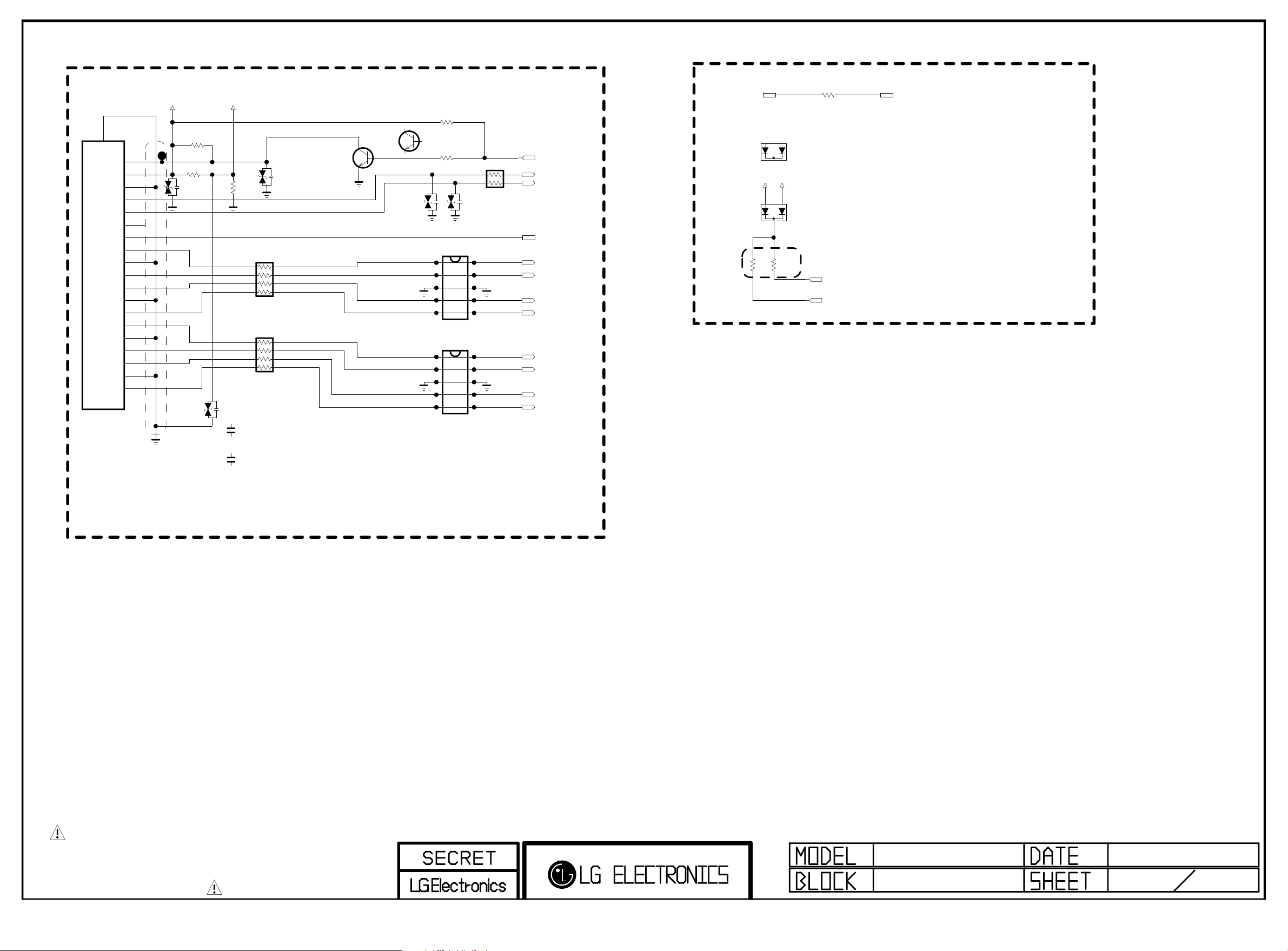
HDMI (REAR)
Copyright ⓒ 2015 LG Electronics. Inc. All right reserved.
Only for training and service purposes
LGE Internal Use Only
HDMI_1
5V_HDMI_2
SHIELDGND
20
HP_DET
19
5V
18
GND
17
DDC_DATA
ESD_HDMI1_VARISTOR
16
DDC_CLK
15
NC
14
CE_REMOTE
13
CK-
12
CK_GND
11
CK+
10
EAG59023302
JK1000
This GND Pattern should be very narrow
HDMI jack burnt problem improvement
9
8
7
6
5
4
3
2
1
D0-
D0_GND
D0+
D1-
D1_GND
D1+
D2-
D2_GND
D2+
R1001
R1000
1.8K
VA1000
1K
5V_DET_HDMI_2
R1002
3.3K
ESD_HDMI1_VARISTOR
VA1001
ESD_HDMI1_CAP
VA1000-*1
1uF
10V
ESD_HDMI1_CAP
VA1001-*1
1uF
10V
AR1000
5.1
AR1001
5.1
MMBT3904(NXP)
ESD_HDMI1
VA1002
TR_NXP
Q1000
C
E
TR_KEC
Q1000-*1
2N3904S
B
C
B
E
ESD_HDMI1
VA1003
ESD_HDMI1_TMDS
IP4294CZ10-TBR
ESD_HDMI1_TMDS
IP4294CZ10-TBR
1
2
3
4
5
1
2
3
4
5
R1003
10K
R1004
10K
D1000
D1001
AR1002
100
1/16W
ESD_HDMI1
VA1004
10
9
8
7
6
10
9
8
7
6
HPD2
DDC_SDA_2
DDC_SCL_2
HDMI_CEC
CK-_HDMI2
CK+_HDMI2
D0-_HDMI2
D0+_HDMI2
D1-_HDMI2
D1+_HDMI2
D2-_HDMI2
D2+_HDMI2
CEC
HDMI_CEC
HDMI_DIODE_SUZHOU
D1002-*1
MMBD6100
A1
C
R1007
2.7K
+5V_Normal
R1008
2.7K
5V_HDMI_2
R1009
100
A2
HDMI_DIODE_KEC
A2CA1
KDS184
D1002
DDC_SDA_2
DDC_SCL_2
CEC_REMOTE_S7
THE SYMBOL MARK OF THIS SCHEMETIC DIAGRAM INCORPORATES
SPECIAL FEATURES IMPORTANT FOR PROTECTION FROM X-RADIATION.
FIRE AND ELECTRICAL SHOCK HAZARDS, WHEN SERVICING IF IS
ESSENTIAL THAT ONLY MANUFACTURES SPECIFIED PARTS BE USED FOR
THE CRITICAL COMPONENTS IN THE SYMBOL MARK OF THE SCHEMETIC.
L15.5
2015/01/21
HDMI_R1S1 8
Page 22
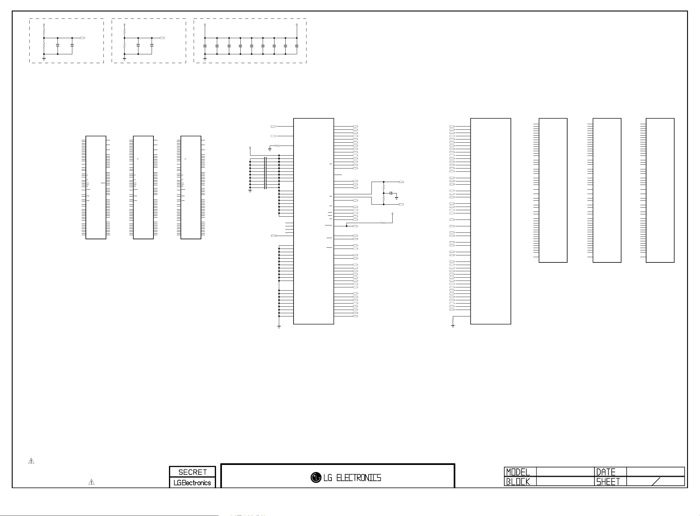
DDR_EXT
Copyright ⓒ 2015 LG Electronics. Inc. All right reserved.
Only for training and service purposes
LGE Internal Use Only
R1201
DDR_EXT
R1202
1K
1%
DDR_EXT
1K
1%
CLose to DDR3
DDR_EXT
C1201
C1202
0.1uF
1000pF
A-MVREFDQ
+1.5V_DDR+1.5V_DDR
DDR_EXT
R1204
DDR_EXT
R1205
1K
1%
1K
1%
CLose to MAIN IC
DDR_EXT
DDR_EXT
C1213
C1214
0.1uF
1000pF
A-MVREFCA
+1.5V_DDR
Option : Ripple Check !!!
OPT
C1217
0.1uF
C1218
0.1uF
OPT
C1216
10uF
10V
OPT
C1219
+1.5V_DDR
OPT
OPT
OPT
C1221
OPT
C1222
1uF
1uF
C1220
1uF
1uF
C1223
OPT
OPT
C1224
0.1uF
1uF
DDR_1600_1G_NAN
IC1201-*1
NT5CB64M16FP-DH
EAN61859502
N3
A0
P7
A1
P3
A2
N2
A3
P8
A4
P2
A5
R8
A6
R2
A7
T8
A8
R3
A9
L7
A10/AP
R7
A11
N7
A12
T3
NC_6
M7
NC_5
M2
BA0
N8
BA1
M3
BA2
J7
CK
K7
CK
K9
CKE
L2
CS
K1
ODT
J3
RAS
K3
CAS
L3
WE
T2
RESET
F3
DQSL
G3
DQSL
C7
DQSU
B7
DQSU
E7
DML
D3
DMU
E3
DQL0
F7
DQL1
F2
DQL2
F8
DQL3
H3
DQL4
H8
DQL5
G2
DQL6
H7
DQL7
D7
DQU0
C3
DQU1
C8
DQU2
C2
DQU3
A7
DQU4
A2
DQU5
B8
DQU6
A3
DQU7
DDR_1600_1G_SS
IC1201
K4B1G1646G-BCK0
EAN61836301
DDR_EXT
R1203
240 1%
M8
VREFCA
H1
VREFDQ
L8
ZQ
B2
VDD_1
D9
VDD_2
G7
VDD_3
K2
VDD_4
K8
VDD_5
N1
VDD_6
N9
VDD_7
R1
VDD_8
R9
VDD_9
A1
VDDQ_1
A8
VDDQ_2
C1
VDDQ_3
C9
VDDQ_4
D2
VDDQ_5
E9
VDDQ_6
F1
VDDQ_7
H2
VDDQ_8
H9
VDDQ_9
J1
NC_1
J9
NC_2
L1
NC_3
L9
NC_4
T7
NC_6
A9
VSS_1
B3
VSS_2
E1
VSS_3
G8
VSS_4
J2
VSS_5
J8
VSS_6
M1
VSS_7
M9
VSS_8
P1
VSS_9
P9
VSS_10
T1
VSS_11
T9
VSS_12
B1
VSSQ_1
B9
VSSQ_2
D1
VSSQ_3
D8
VSSQ_4
E2
VSSQ_5
E8
VSSQ_6
F9
VSSQ_7
G1
VSSQ_8
G9
VSSQ_9
+1.5V_DDR
A-MVREFCA
A-MVREFDQ
C1203 10uF 10V
C1204 0.1uF
C1205 0.1uF
C1206 0.1uF
C1207 0.1uF
C1208 0.1uF
C1209 0.1uF
C1210 0.1uF
C1211 0.1uF
C1212 0.1uF
A-MA14
DDR_1600_2G_SS
IC1201-*2
K4B2G1646Q-BCK0
M8
VREFCA
H1
VREFDQ
L8
ZQ
B2
VDD_1
D9
VDD_2
G7
VDD_3
K2
VDD_4
K8
VDD_5
N1
VDD_6
N9
VDD_7
R1
VDD_8
R9
VDD_9
A1
VDDQ_1
A8
VDDQ_2
C1
VDDQ_3
C9
VDDQ_4
D2
VDDQ_5
E9
VDDQ_6
F1
VDDQ_7
H2
VDDQ_8
H9
VDDQ_9
J1
NC_1
J9
NC_2
L1
NC_3
L9
NC_4
T7
NC_7
A9
VSS_1
B3
VSS_2
E1
VSS_3
G8
VSS_4
J2
VSS_5
J8
VSS_6
M1
VSS_7
M9
VSS_8
P1
VSS_9
P9
VSS_10
T1
VSS_11
T9
VSS_12
B1
VSSQ_1
B9
VSSQ_2
D1
VSSQ_3
D8
VSSQ_4
E2
VSSQ_5
E8
VSSQ_6
F9
VSSQ_7
G1
VSSQ_8
G9
VSSQ_9
N3
P7
P3
N2
P8
P2
R8
R2
T8
R3
L7
R7
N7
T3
M7
M2
N8
M3
J7
K7
K9
L2
K1
J3
K3
L3
T2
F3
G3
C7
B7
E7
D3
E3
F7
F2
F8
H3
H8
G2
H7
D7
C3
C8
C2
A7
A2
B8
A3
EAN61848803
A0
A1
A2
A3
A4
A5
A6
A7
A8
A9
A10/AP
A11
A12/BC
A13
NC_5
BA0
BA1
BA2
CK
CK
CKE
CS
ODT
RAS
CAS
WE
RESET
DQSL
DQSL
DQSU
DQSU
DML
DMU
DQL0
DQL1
DQL2
DQL3
DQL4
DQL5
DQL6
DQL7
DQU0
DQU1
DQU2
DQU3
DQU4
DQU5
DQU6
DQU7
M8
VREFCA
H1
VREFDQ
L8
ZQ
B2
VDD_1
D9
VDD_2
G7
VDD_3
K2
VDD_4
K8
VDD_5
N1
VDD_6
N9
VDD_7
R1
VDD_8
R9
VDD_9
A1
VDDQ_1
A8
VDDQ_2
C1
VDDQ_3
C9
VDDQ_4
D2
VDDQ_5
E9
VDDQ_6
F1
VDDQ_7
H2
VDDQ_8
H9
VDDQ_9
J1
NC_1
J9
NC_2
L1
NC_3
L9
NC_4
T7
NC_6
A9
VSS_1
B3
VSS_2
E1
VSS_3
G8
VSS_4
J2
VSS_5
J8
VSS_6
M1
VSS_7
M9
VSS_8
P1
VSS_9
P9
VSS_10
T1
VSS_11
T9
VSS_12
B1
VSSQ_1
B9
VSSQ_2
D1
VSSQ_3
D8
VSSQ_4
E2
VSSQ_5
E8
VSSQ_6
F9
VSSQ_7
G1
VSSQ_8
G9
VSSQ_9
DDR_1600_2G_SK
IC1201-*3
H5TQ2G63FFR-PBC
EAN61829204
N3
A0
P7
A1
P3
A2
N2
A3
P8
A4
P2
A5
R8
A6
R2
A7
T8
A8
R3
A9
L7
A10/AP
R7
A11
N7
A12/BC
T3
A13
M7
NC_5
M2
BA0
N8
BA1
M3
BA2
J7
CK
K7
CK
K9
CKE
L2
CS
K1
ODT
J3
RAS
K3
CAS
L3
WE
T2
RESET
F3
DQSL
G3
DQSL
C7
DQSU
B7
DQSU
E7
DML
D3
DMU
E3
DQL0
F7
DQL1
F2
DQL2
F8
DQL3
H3
DQL4
H8
DQL5
G2
DQL6
H7
DQL7
D7
DQU0
C3
DQU1
C8
DQU2
C2
DQU3
A7
DQU4
A2
DQU5
B8
DQU6
A3
DQU7
M8
VREFCA
H1
VREFDQ
L8
ZQ
B2
VDD_1
D9
VDD_2
G7
VDD_3
K2
VDD_4
K8
VDD_5
N1
VDD_6
N9
VDD_7
R1
VDD_8
R9
VDD_9
A1
VDDQ_1
A8
VDDQ_2
C1
VDDQ_3
C9
VDDQ_4
D2
VDDQ_5
E9
VDDQ_6
F1
VDDQ_7
H2
VDDQ_8
H9
VDDQ_9
J1
NC_1
J9
NC_2
L1
NC_3
L9
NC_4
T7
NC_6
A9
VSS_1
B3
VSS_2
E1
VSS_3
G8
VSS_4
J2
VSS_5
J8
VSS_6
M1
VSS_7
M9
VSS_8
P1
VSS_9
P9
VSS_10
T1
VSS_11
T9
VSS_12
B1
VSSQ_1
B9
VSSQ_2
D1
VSSQ_3
D8
VSSQ_4
E2
VSSQ_5
E8
VSSQ_6
F9
VSSQ_7
G1
VSSQ_8
G9
VSSQ_9
DDR_EXT
DDR_EXT
DDR_EXT
DDR_EXT
DDR_EXT
DDR_EXT
DDR_EXT
DDR_EXT
DDR_EXT
DDR_EXT
A10/AP
A12/BC
NC_5
RESET
DQSL
DQSL
DQSU
DQSU
DQL0
DQL1
DQL2
DQL3
DQL4
DQL5
DQL6
DQL7
DQU0
DQU1
DQU2
DQU3
DQU4
DQU5
DQU6
DQU7
N3
A0
P7
A1
P3
A2
N2
A3
P8
A4
P2
A5
R8
A6
R2
A7
T8
A8
R3
A9
L7
R7
A11
N7
T3
A13
M7
M2
BA0
N8
BA1
M3
BA2
J7
CK
K7
CK
K9
CKE
L2
CS
K1
ODT
J3
RAS
K3
CAS
L3
WE
T2
F3
G3
C7
B7
E7
DML
D3
DMU
E3
F7
F2
F8
H3
H8
G2
H7
D7
C3
C8
C2
A7
A2
B8
A3
A-MA0
A-MA1
A-MA2
A-MA3
A-MA4
A-MA5
A-MA6
A-MA7
A-MA8
A-MA9
A-MA10
A-MA11
A-MA12
A-MA13
A-MBA0
A-MBA1
A-MBA2
A-MCKE
A/B_DDR3_CS
A-MODT
A-MRASB
A-MCASB
A-MWEB
A-MRESETB
A-MDQSL
A-MDQSLB
A-MDQSU
A-MDQSUB
A-MDML
A-MDMU
A-MDQL0
A-MDQL1
A-MDQL2
A-MDQL3
A-MDQL4
A-MDQL5
A-MDQL6
A-MDQL7
A-MDQU0
A-MDQU1
A-MDQU2
A-MDQU3
A-MDQU4
A-MDQU5
A-MDQU6
A-MDQU7
DDR_EXT
R1207
DDR_EXT
R1208
56
1%
56
1%
DDR_EXT
R1206
10K
DDR_EXT
C1215
0.01uF
50V
+1.5V_DDR
A-MCK
A-MCKB
A-MA0
A-MA1
A-MA2
A-MA3
A-MA4
A-MA5
A-MA6
A-MA7
A-MA8
A-MA9
A-MA10
A-MA11
A-MA12
A-MA13
A-MA14
A-MBA0
A-MBA1
A-MBA2
A-MCK
A-MCKB
A-MCKE
A-MODT
A-MRASB
A-MCASB
A-MWEB
A-MRESETB
A/B_DDR3_CS
A-MDQSL
A-MDQSU
A-MDML
A-MDMU
A-MDQSLB
A-MDQSUB
A-MDQL0
A-MDQL1
A-MDQL2
A-MDQL3
A-MDQL4
A-MDQL5
A-MDQL6
A-MDQL7
A-MDQU0
A-MDQU1
A-MDQU2
A-MDQU3
A-MDQU4
A-MDQU5
A-MDQU6
A-MDQU7
R1209
240
1%
M1A_256M_UO4
LGE2134(256M)
E11
B_DDR3_A[0]
F12
B_DDR3_A[1]
D10
B_DDR3_A[2]
B10
B_DDR3_A[3]
E15
B_DDR3_A[4]
B11
B_DDR3_A[5]
F14
B_DDR3_A[6]
C11
B_DDR3_A[7]
D14
B_DDR3_A[8]
A12
B_DDR3_A[9]
F16
B_DDR3_A[10]
D13
B_DDR3_A[11]
D15
B_DDR3_A[12]
C12
B_DDR3_A[13]
E13
B_DDR3_A[14]
A9
B_DDR3_BA[0]
D16
B_DDR3_BA[1]
A10
B_DDR3_BA[2]
C13
B_DDR3_MCLK
B13
B_DDR3_MCLKZ
E17
B_DDR3_MCLKE
B8
B_DDR3_ODT
C8
B_DDR3_RASZ
B9
B_DDR3_CASZ
D11
B_DDR3_WEZ
F10
B_RESET
D12
B_DDR3_CS0
A19
B_DDR3_DQSL
B18
B_DDR3_DQSU
C16
B_DDR3_DQML
D21
B_DDR3_DQMU
C18
B_DDR3_DQSBL
C17
B_DDR3_DQSBU
A20
B_DDR3_DQL[0]
A16
B_DDR3_DQL[1]
C19
B_DDR3_DQL[2]
C15
B_DDR3_DQL[3]
C20
B_DDR3_DQL[4]
C14
B_DDR3_DQL[5]
B21
B_DDR3_DQL[6]
B15
B_DDR3_DQL[7]
F18
B_DDR3_DQU[0]
D19
B_DDR3_DQU[1]
D17
B_DDR3_DQU[2]
E21
B_DDR3_DQU[3]
E19
B_DDR3_DQU[4]
D20
B_DDR3_DQU[5]
D18
B_DDR3_DQU[6]
F20
B_DDR3_DQU[7]
E9
ZQ
IC101
E11
F12
D10
B10
E15
B11
F14
C11
D14
A12
F16
D13
D15
C12
E13
A9
D16
A10
C13
B13
E17
B8
C8
B9
D11
F10
D12
A19
B18
C16
D21
C18
C17
A20
A16
C19
C15
C20
C14
B21
B15
F18
D19
D17
E21
E19
D20
D18
F20
E9
B_DDR3_A[0]
B_DDR3_A[1]
B_DDR3_A[2]
B_DDR3_A[3]
B_DDR3_A[4]
B_DDR3_A[5]
B_DDR3_A[6]
B_DDR3_A[7]
B_DDR3_A[8]
B_DDR3_A[9]
B_DDR3_A[10]
B_DDR3_A[11]
B_DDR3_A[12]
B_DDR3_A[13]
B_DDR3_A[14]
B_DDR3_BA[0]
B_DDR3_BA[1]
B_DDR3_BA[2]
B_DDR3_MCLK
B_DDR3_MCLKZ
B_DDR3_MCLKE
B_DDR3_ODT
B_DDR3_RASZ
B_DDR3_CASZ
B_DDR3_WEZ
B_RESET
B_DDR3_CS0
B_DDR3_DQSL
B_DDR3_DQSU
B_DDR3_DQML
B_DDR3_DQMU
B_DDR3_DQSBL
B_DDR3_DQSBU
B_DDR3_DQL[0]
B_DDR3_DQL[1]
B_DDR3_DQL[2]
B_DDR3_DQL[3]
B_DDR3_DQL[4]
B_DDR3_DQL[5]
B_DDR3_DQL[6]
B_DDR3_DQL[7]
B_DDR3_DQU[0]
B_DDR3_DQU[1]
B_DDR3_DQU[2]
B_DDR3_DQU[3]
B_DDR3_DQU[4]
B_DDR3_DQU[5]
B_DDR3_DQU[6]
B_DDR3_DQU[7]
ZQ
M1A_128M_UO4
IC101-*1
LGE2133(128M)
M1A_256M_AVS+
LGE2136(256M)
E11
B_DDR3_A[0]
F12
B_DDR3_A[1]
D10
B_DDR3_A[2]
B10
B_DDR3_A[3]
E15
B_DDR3_A[4]
B11
B_DDR3_A[5]
F14
B_DDR3_A[6]
C11
B_DDR3_A[7]
D14
B_DDR3_A[8]
A12
B_DDR3_A[9]
F16
B_DDR3_A[10]
D13
B_DDR3_A[11]
D15
B_DDR3_A[12]
C12
B_DDR3_A[13]
E13
B_DDR3_A[14]
A9
B_DDR3_BA[0]
D16
B_DDR3_BA[1]
A10
B_DDR3_BA[2]
C13
B_DDR3_MCLK
B13
B_DDR3_MCLKZ
E17
B_DDR3_MCLKE
B8
B_DDR3_ODT
C8
B_DDR3_RASZ
B9
B_DDR3_CASZ
D11
B_DDR3_WEZ
F10
B_RESET
D12
B_DDR3_CS0
A19
B_DDR3_DQSL
B18
B_DDR3_DQSU
C16
B_DDR3_DQML
D21
B_DDR3_DQMU
C18
B_DDR3_DQSBL
C17
B_DDR3_DQSBU
A20
B_DDR3_DQL[0]
A16
B_DDR3_DQL[1]
C19
B_DDR3_DQL[2]
C15
B_DDR3_DQL[3]
C20
B_DDR3_DQL[4]
C14
B_DDR3_DQL[5]
B21
B_DDR3_DQL[6]
B15
B_DDR3_DQL[7]
F18
B_DDR3_DQU[0]
D19
B_DDR3_DQU[1]
D17
B_DDR3_DQU[2]
E21
B_DDR3_DQU[3]
E19
B_DDR3_DQU[4]
D20
B_DDR3_DQU[5]
D18
B_DDR3_DQU[6]
F20
B_DDR3_DQU[7]
E9
ZQ
IC101-*2
M1A_128M_AVS+
LGE2135(128M)
E11
B_DDR3_A[0]
F12
B_DDR3_A[1]
D10
B_DDR3_A[2]
B10
B_DDR3_A[3]
E15
B_DDR3_A[4]
B11
B_DDR3_A[5]
F14
B_DDR3_A[6]
C11
B_DDR3_A[7]
D14
B_DDR3_A[8]
A12
B_DDR3_A[9]
F16
B_DDR3_A[10]
D13
B_DDR3_A[11]
D15
B_DDR3_A[12]
C12
B_DDR3_A[13]
E13
B_DDR3_A[14]
A9
B_DDR3_BA[0]
D16
B_DDR3_BA[1]
A10
B_DDR3_BA[2]
C13
B_DDR3_MCLK
B13
B_DDR3_MCLKZ
E17
B_DDR3_MCLKE
B8
B_DDR3_ODT
C8
B_DDR3_RASZ
B9
B_DDR3_CASZ
D11
B_DDR3_WEZ
F10
B_RESET
D12
B_DDR3_CS0
A19
B_DDR3_DQSL
B18
B_DDR3_DQSU
C16
B_DDR3_DQML
D21
B_DDR3_DQMU
C18
B_DDR3_DQSBL
C17
B_DDR3_DQSBU
A20
B_DDR3_DQL[0]
A16
B_DDR3_DQL[1]
C19
B_DDR3_DQL[2]
C15
B_DDR3_DQL[3]
C20
B_DDR3_DQL[4]
C14
B_DDR3_DQL[5]
B21
B_DDR3_DQL[6]
B15
B_DDR3_DQL[7]
F18
B_DDR3_DQU[0]
D19
B_DDR3_DQU[1]
D17
B_DDR3_DQU[2]
E21
B_DDR3_DQU[3]
E19
B_DDR3_DQU[4]
D20
B_DDR3_DQU[5]
D18
B_DDR3_DQU[6]
F20
B_DDR3_DQU[7]
E9
ZQ
IC101-*3
THE SYMBOL MARK OF THIS SCHEMETIC DIAGRAM INCORPORATES
SPECIAL FEATURES IMPORTANT FOR PROTECTION FROM X-RADIATION.
FIRE AND ELECTRICAL SHOCK HAZARDS, WHEN SERVICING IF IS
ESSENTIAL THAT ONLY MANUFACTURES SPECIFIED PARTS BE USED FOR
THE CRITICAL COMPONENTS IN THE SYMBOL MARK OF THE SCHEMETIC.
L14_CA_M1A
DDR
2014/06/13
12
Page 23
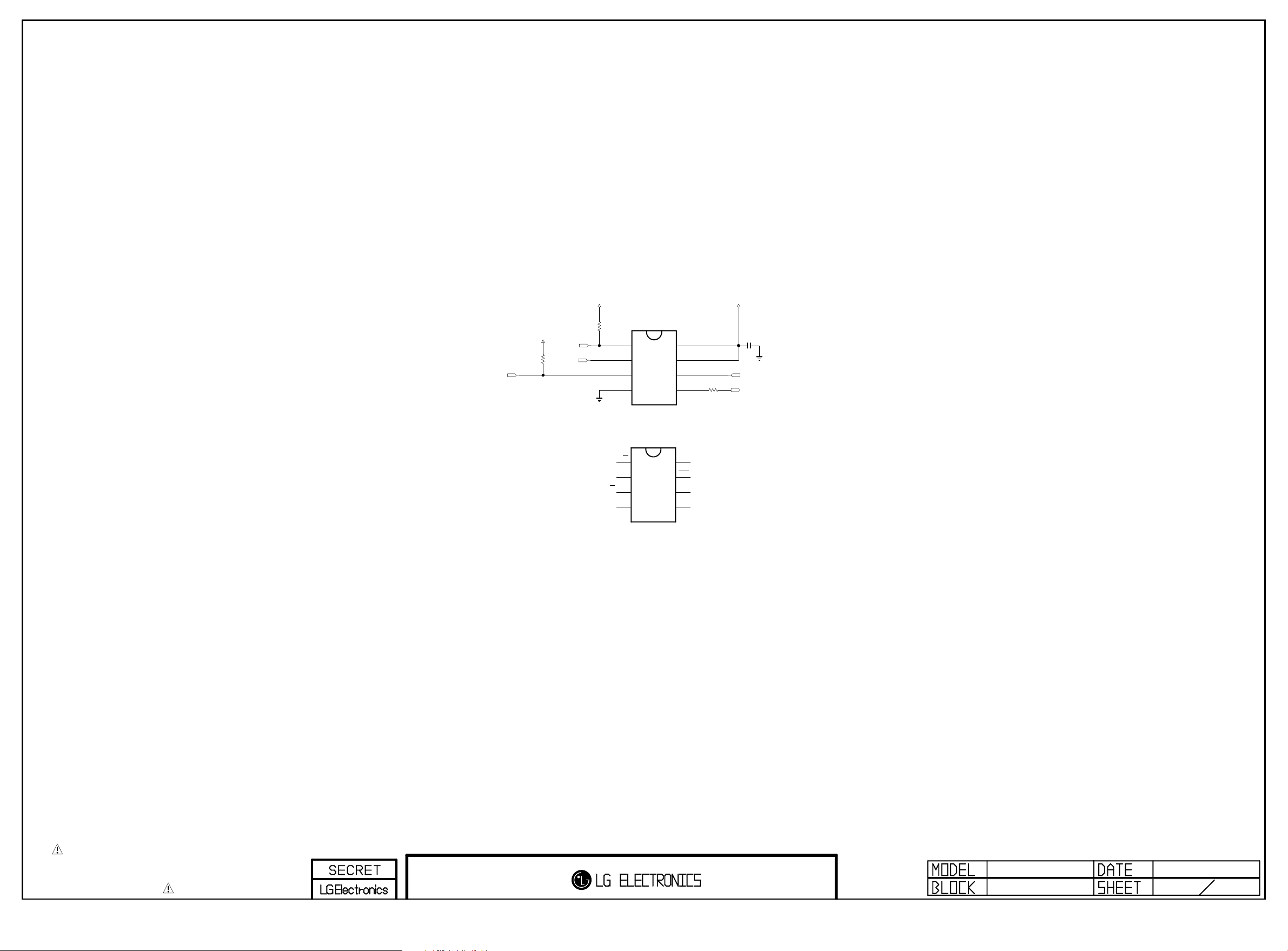
Serial Flash for SPI boot
Copyright ⓒ 2015 LG Electronics. Inc. All right reserved.
Only for training and service purposes
LGE Internal Use Only
/FLASH_WP
OPT
R1300
10K
+3.5V_ST
/SPI_CS
SPI_SDO
R1301
4.7K
OPT
WP#/SIO2
SPI_FLASH_MACRONIX
IC1300
MX25L8035EM2I-10G
CS#
1
SO/SIO1
2
3
GND
4
SPI_FLASH_WINBOND
IC1300-*1
W25Q80DVSSIG
CS
1
DO[IO1]
2
WP[IO2]
3
GND
4
8
7
6
5
8
7
6
5
VCC
NC/SIO3
SCLK
SI/SIO0
VCC
HOLD[IO3]
CLK
DI[IO0]
R1302
33
+3.5V_ST+3.5V_ST
C1300
0.1uF
16V
SPI_SCK
SPI_SDI
THE SYMBOL MARK OF THIS SCHEMETIC DIAGRAM INCORPORATES
SPECIAL FEATURES IMPORTANT FOR PROTECTION FROM X-RADIATION.
FIRE AND ELECTRICAL SHOCK HAZARDS, WHEN SERVICING IF IS
ESSENTIAL THAT ONLY MANUFACTURES SPECIFIED PARTS BE USED FOR
THE CRITICAL COMPONENTS IN THE SYMBOL MARK OF THE SCHEMETIC.
L15.5_ECI_M1A
S_FLASH
140721
13
Page 24
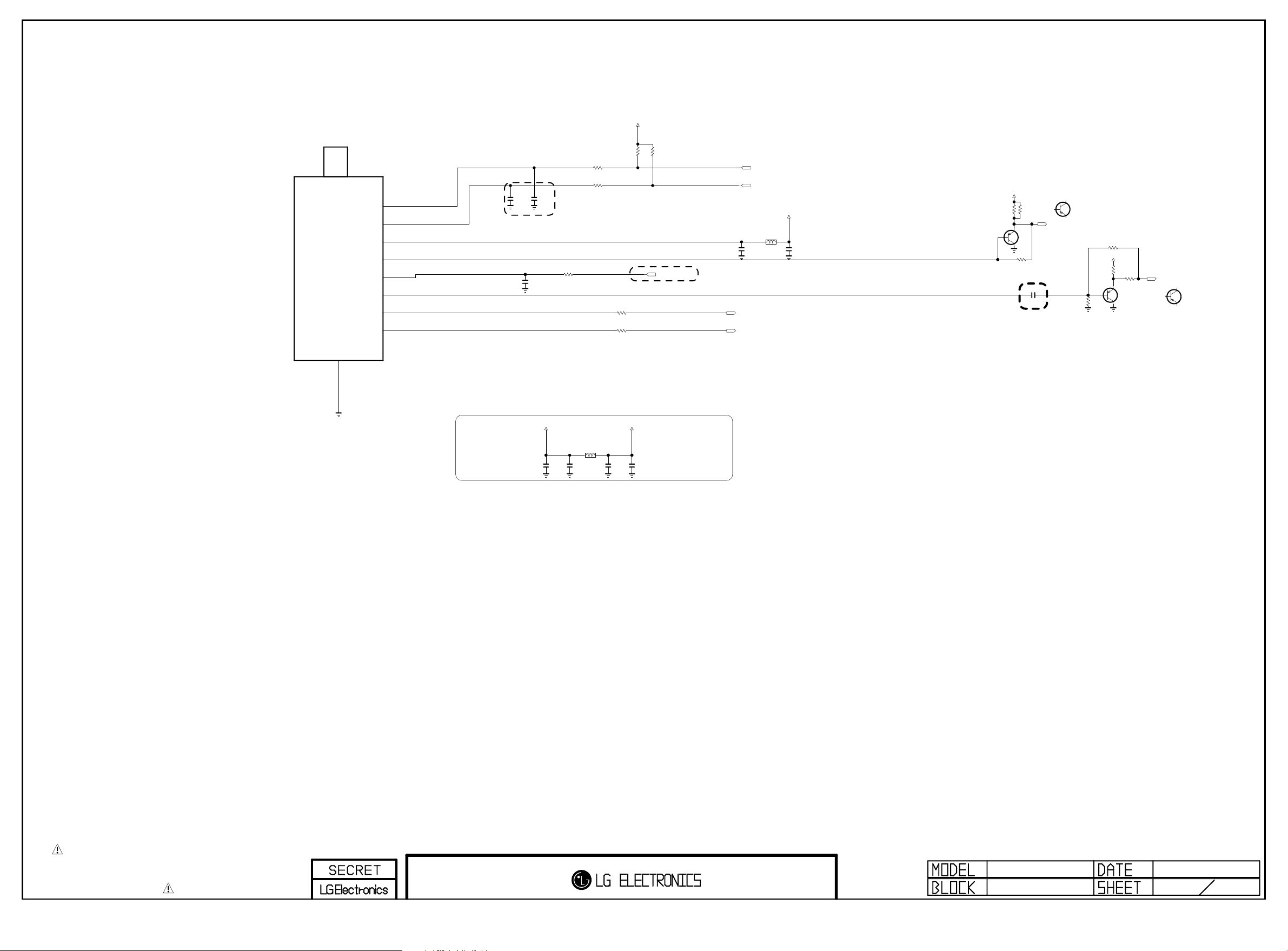
Central and South Americatuner block
Copyright ⓒ 2015 LG Electronics. Inc. All right reserved.
Only for training and service purposes
LGE Internal Use Only
+3.3V_TU
R1428
TU3901
TDJA-T101F(A)
1
2
3
4
5
6
7
8
9
SHIELD
SCL
SDA
B[+3.3V]
CVBS
IF_AGC
SIF
IF[N]
IF[P]
Close to Tuner
C1412
18pF
50V
C1414
18pF
50V
HALF_NIM/BRAZIL
C1404
0.1uF
16V
HALF_NIM/BRAZIL
R1405
R1427
33
33
HALF_NIM/BRAZIL
R1404
HALF_NIM/BRAZIL
10
R1403
10
1K
R1411
R1425
100
1K
should be guarded by ground
IF_AGC_MAIN
TU_SCL
TU_SDA
C1405
100pF
50V
IF_N_MSTAR
IF_P_MSTAR
+3.3V_TU
L1401
UBW2012-121F
C1408
0.1uF
16V
+3.3V_TU
CVBS
CVBS
R3732
R3735
220
220
E
CVBS_NXP
Q3701
MMBT3906(NXP)
B
C
OPT
R3731
0
SIF
C3726
0.1uF
16V
close to TUNER
B
TU_CVBS
C
CVBS_KEC
Q3701-*1
2N3906S-RTK
E
SIGN37000000
SIF
R3724
4.7K
OPT
R3726
0
+3.3V_TU
SIF
R3725
470
SIGN37000001
B
SIF
R3728
82
E
SIF_NXP
Q3700
MMBT3906(NXP)
C
TU_SIF
B
C
SIF_KEC
Q3700-*1
2N3906S-RTK
E
+3.3V_TU
C1418
22uF
10V
L1400
UBW2012-121F
C1419
0.1uF
16V
+3.3V_Normal
C1422
C1420
0.1uF
22uF
16V
10V
THE SYMBOL MARK OF THIS SCHEMETIC DIAGRAM INCORPORATES
SPECIAL FEATURES IMPORTANT FOR PROTECTION FROM X-RADIATION.
FIRE AND ELECTRICAL SHOCK HAZARDS, WHEN SERVICING IF IS
ESSENTIAL THAT ONLY MANUFACTURES SPECIFIED PARTS BE USED FOR
THE CRITICAL COMPONENTS IN THE SYMBOL MARK OF THE SCHEMETIC.
L14_CA_M1A
TUNER_CSA
2014.08.11
14
Page 25
LVDS
Copyright ⓒ 2015 LG Electronics. Inc. All right reserved.
Only for training and service purposes
LGE Internal Use Only
[51Pin LVDS Connector]
(For FHD 60Hz)
MO_FHD
P1800
SP14-11592-01-51Pin
1
2
3
4
5
6
7
8
9
10
11
12
13
14
15
16
17
18
19
20
21
22
23
24
25
26
27
28
29
30
31
32
33
34
35
36
37
38
39
40
41
42
43
44
45
46
47
48
49
50
51
52
PANEL_VCC
C1800
0.1uF
25V
RXA4+
RXA4-
RXA3+
RXA3-
RXACK+
RXACK-
RXA2+
RXA2-
RXA1+
RXA1-
RXA0+
RXA0-
RXB4+
RXB4-
RXB3+
RXB3-
RXBCK+
RXBCK-
RXB2+
RXB2-
RXB1+
RXB1-
RXB0+
RXB0-
UBW2012-121F
OPT
AR1800
1/16W
L1801
PANEL_HD
C1801
10uF
25V
[30Pin LVDS Connector]
(For HD 60Hz_Normal)
MO_HD
P1801
10031HR-30
1
2
3
4
5
6
7
8
9
10
11
12
13
14
15
16
17
18
19
20
21
22
OPT
R1801
0
0
R1812
OPT
0
23
24
25
26
27
28
29
30
31
RXA3+
RXA3-
RXACK+
RXACK-
RXA2+
RXA2-
RXA1+
RXA1-
RXA0+
RXA0-
PANEL_HD
THE SYMBOL MARK OF THIS SCHEMETIC DIAGRAM INCORPORATES
SPECIAL FEATURES IMPORTANT FOR PROTECTION FROM X-RADIATION.
FIRE AND ELECTRICAL SHOCK HAZARDS, WHEN SERVICING IF IS
ESSENTIAL THAT ONLY MANUFACTURES SPECIFIED PARTS BE USED FOR
THE CRITICAL COMPONENTS IN THE SYMBOL MARK OF THE SCHEMETIC.
L14_CA_M1A
LVDS
140613
18
Page 26
SCART_COMPONENT
Copyright ⓒ 2015 LG Electronics. Inc. All right reserved.
Only for training and service purposes
LGE Internal Use Only
COMPONENT
COMP
JK2601
PPJ245N2-01
[RD2]E-LUG
6E
[RD2]O-SPRING
5E
[RD2]CONTACT
4E
[WH]O-SPRING
5D
[RD1]CONTACT
4C
[RD1]O-SPRING
5C
[RD1]E-LUG-S
7C
[BL]O-SPRING
5B
[GN/YL]CONTACT
4A
[GN/YL]O-SPRING
5A
[GN/YL]E-LUG
6A
ESD_COMP_ZENER_ROHM
ESD_COMP_ZENER_ROHM
ESD_COMP_ZENER_ROHM
ESD_COMP_ZENER_ROHM
ZD2601-*1
ESD_COMP_ZENER_KEC
ZD2602-*1
ESD_COMP_ZENER_KEC
ZD2603-*1
ESD_COMP_ZENER_KEC
ZD2604-*1
ESD_COMP_ZENER_KEC
ZD2605-*1
ESD_COMP_ZENER_KEC
ZD2606-*1
ESD_COMP_ZENER_KEC
ZD2605
ZD2606
ZD2603
ZD2604
ESD_COMP_ZENER_ROHM
ESD_COMP_ZENER_ROHM
OPT
VA2601
5.6V
OPT
VA2602
5.6V
ESD_COMP
VA2603
5.5V
ESD_COMP
VA2604
5.5V
OPT
VA2605
5.6V
ZD2601
ZD2602
R2601
470K
COMP
R2602
470K
COMP
COMP
R2603
COMP
R2604
COMP
R2606
10K
COMP
ATV_330P
330pF
C2601
COMP
R2607
10K
ATV_330P
330pF
C2602
75
75
COMP
R2605
75
3216
R2608
12K
COMP
R2609
12K
COMP2_R_IN
COMP2_L_IN
COMP2_Pr+
COMP2_Pb+
COMP2_Y+/AV_CVBS_IN
+3.3V_Normal
+3.3V_Normal
COMP
R2611
10K
COMP
R2610
10K
OPT
VA2606
5.6V
OPT
C2603
0.1uF
16V
COMP
R2612
COMP
R2613
1K
1K
COMP2_DET
AV_CVBS_DET
THE SYMBOL MARK OF THIS SCHEMETIC DIAGRAM INCORPORATES
SPECIAL FEATURES IMPORTANT FOR PROTECTION FROM X-RADIATION.
FIRE AND ELECTRICAL SHOCK HAZARDS, WHEN SERVICING IF IS
ESSENTIAL THAT ONLY MANUFACTURES SPECIFIED PARTS BE USED FOR
THE CRITICAL COMPONENTS IN THE SYMBOL MARK OF THE SCHEMETIC.
L15.5_ECI
COMPONENT
2015/02/27
26
Page 27
RS-232C 4PIN
Copyright ⓒ 2015 LG Electronics. Inc. All right reserved.
Only for training and service purposes
LGE Internal Use Only
RS-232C 4PIN
+3.5V_ST
PM_RXD
PM_TXD
AR4000
100
1/16W
MSTAR DEBUG 4PIN
RS232C_DEBUG_4P
VCC
PM_RXD
GND
RM_TXD
P4000
12507WS-04L
1
2
3
4
5
GND
JP_GND1
JP_GND2
JP_GND3
JP_GND4
THE SYMBOL MARK OF THIS SCHEMETIC DIAGRAM INCORPORATES
SPECIAL FEATURES IMPORTANT FOR PROTECTION FROM X-RADIATION.
FIRE AND ELECTRICAL SHOCK HAZARDS, WHEN SERVICING IF IS
ESSENTIAL THAT ONLY MANUFACTURES SPECIFIED PARTS BE USED FOR
THE CRITICAL COMPONENTS IN THE SYMBOL MARK OF THE SCHEMETIC.
L14_CA_M1A
RS232C_MSTAR_DEBUG_4P
2014/05/22
40
Page 28
KEY1
Copyright ⓒ 2015 LG Electronics. Inc. All right reserved.
Only for training and service purposes
LGE Internal Use Only
KEY2
IR
+3.5V_ST
LED_R/BUZZ
+3.5V_ST
AR4601
10K
1/16W
C4601
0.1uF
R4606
100
OPT
C4604
0.1uF
16V
OPT
C4602
1000pF
50V
16V
IR
R4601
1.8K
+3.5V_ST
R4602
3.3K
C4605
100pF
50V
OPT
VR4602
ZD4601
OPT
5V
IR_6P
P4602
12507WR-06L
1
2
3
4
5
6
7
THE SYMBOL MARK OF THIS SCHEMETIC DIAGRAM INCORPORATES
SPECIAL FEATURES IMPORTANT FOR PROTECTION FROM X-RADIATION.
FIRE AND ELECTRICAL SHOCK HAZARDS, WHEN SERVICING IF IS
ESSENTIAL THAT ONLY MANUFACTURES SPECIFIED PARTS BE USED FOR
THE CRITICAL COMPONENTS IN THE SYMBOL MARK OF THE SCHEMETIC.
L15.5_CI_M1A
IR
2015/01/12
47
Page 29
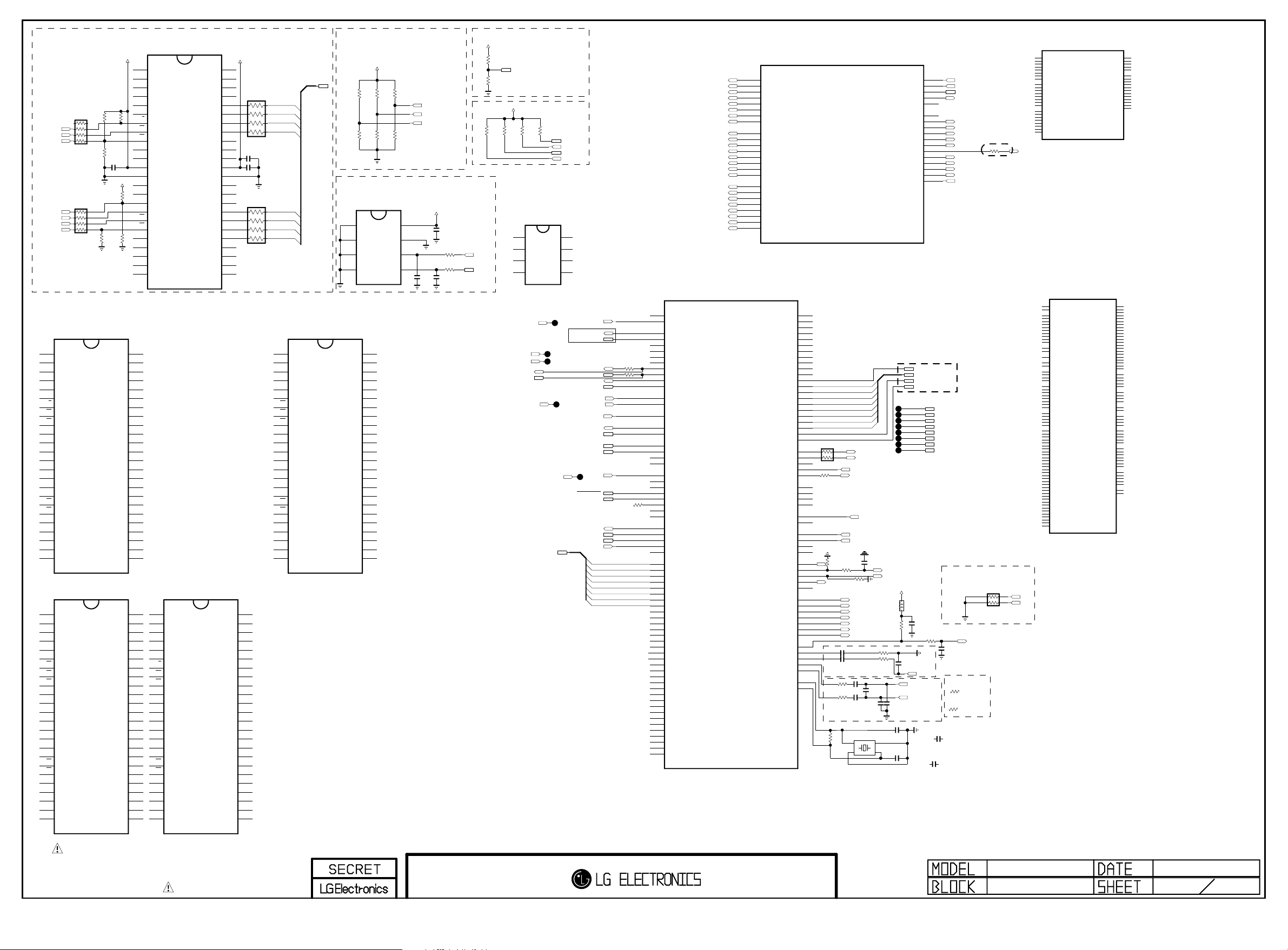
NAND FLASH MEMORY
Copyright ⓒ 2015 LG Electronics. Inc. All right reserved.
Only for training and service purposes
LGE Internal Use Only
AR103
R107
22
/F_RB
/PF_OE
/PF_CE0
R108
+3.3V_Normal
AR104
NAND_FLASH_2G_HYNIX
EAN60708703
H27U2G8F2DTR-BD
1
2
3
4
5
6
7
RE
8
CE
9
10
11
12
13
14
15
16
17
WE
18
WP
19
20
21
22
23
24
NAND_FLASH_2G_TOSHIBA
TC58NVG1S3HTA00
1
2
3
4
5
6
7
RE
8
CE
9
10
11
12
13
14
15
16
17
WE
18
WP
19
20
21
22
23
24
22
R102
3.3K
IC102-*1
EAN60991002
IC102-*3
/PF_CE1
NC_1
NC_2
NC_3
NC_4
NC_5
NC_6
R/B
NC_7
NC_8
VCC_1
VSS_1
NC_9
NC_10
CLE
ALE
NC_11
NC_12
NC_13
NC_14
NC_15
NC_1
NC_2
NC_3
NC_4
NC_5
NC_6
RY/BY
NC_7
NC_8
VCC_1
VSS_1
NC_9
NC_10
CLE
ALE
NC_11
NC_12
NC_13
NC_14
NC_15
PF_ALE
/PF_WE
/PF_WP
1K
OPT
1K
+3.3V_Normal
R109
3.9K
C101
0.1uF
OPT
R105
1K
R106
1K
48
47
46
45
44
43
42
41
40
39
38
37
36
35
34
33
32
31
30
29
28
27
26
25
48
47
46
45
44
43
42
41
40
39
38
37
36
35
34
33
32
31
30
29
28
27
26
25
NC_1
NC_2
NC_3
NC_4
NC_5
NC_6
R/B
RE
CE
NC_7
NC_8
VCC_1
VSS_1
NC_9
NC_10
CLE
ALE
WE
WP
NC_11
NC_12
NC_13
NC_14
NC_15
NC_29
NC_28
NC_27
NC_26
I/O7
I/O6
I/O5
I/O4
NC_25
NC_24
NC_23
VCC_2
VSS_2
NC_22
NC_21
NC_20
I/O3
I/O2
I/O1
I/O0
NC_19
NC_18
NC_17
NC_16
NC_29
NC_28
NC_27
NC_26
I/O8
I/O7
I/O6
I/O5
NC_25
NC_24
NC_23
VCC_2
VSS_2
NC_22
NC_21
NC_20
I/O4
I/O3
I/O2
I/O1
NC_19
NC_18
NC_17
NC_16
NAND_FLASH_1G_HYNIX
H27U1G8F2CTR-BC
EAN35669103
1
2
3
4
5
6
7
8
9
10
11
12
13
14
15
16
17
18
19
20
21
22
23
24
NC_1
1
NC_2
2
NC_3
3
NC_4
4
NC_5
5
NC_6
6
R/B
7
RE
8
CE
9
NC_7
10
NC_8
11
VCC_1
12
VSS_1
13
NC_9
14
NC_10
15
CLE
16
ALE
17
WE
18
WP
19
NC_11
20
NC_12
21
NC_13
22
NC_14
23
NC_15
24
IC102
NAND_FLASH_1G_SS
EAN61857001
IC102-*4
K9F1G08U0D-SCB0
48
47
46
45
44
43
42
41
40
39
38
37
36
35
34
33
32
31
30
29
28
27
26
25
+3.3V_Normal
NC_29
NC_28
NC_27
NC_26
I/O7
I/O6
I/O5
I/O4
NC_25
NC_24
NC_23
VCC_2
C103
VSS_2
0.1uF
NC_22
NC_21
NC_20
I/O3
I/O2
I/O1
I/O0
NC_19
NC_18
NC_17
NC_16
NC_29
48
NC_28
47
NC_27
46
NC_26
45
I/O7
44
I/O6
43
I/O5
42
I/O4
41
NC_25
40
NC_24
39
NC_23
38
VCC_2
37
VSS_2
36
NC_22
35
NC_21
34
NC_20
33
I/O3
32
I/O2
31
I/O1
30
I/O0
29
NC_19
28
NC_18
27
NC_17
26
NC_16
25
AR101
C102
10uF
10V
AR102
R111
R112
22
22
PM MODEL OPTION
+3.5V_ST
LCD
R177
10K
PDP
R176
10K
I2C
R140
1K
PM_MODEL_OPT_0
- HIGH : LCD
- LOW :: PDP
PM_MODEL_OPT_1
- Not Use (Ready)
PM_MODEL_OPT_0
+3.3V_Normal
R144
R141
2.2K
1K
NVRAM_ATMEL
AT24C256C-SSHL-T
A0
I2C_SCL
I2C_SDA
A1
A2
GND
EAN61133501
5V_DET_HDMI_4
DEMOD_SCL
DEMOD_SDA
AMP_SCL
AMP_SDA
R145
2.2K
IC104-*1
1
2
3
4
PCM_A[0-7]
HP_DET
I2C_SDA
I2C_SCL
AMP_SDA
AMP_SCL
VCC
8
WP
7
SCL
6
SDA
5
5V_DET_HDMI_4
AV2_CVBS_DETAV2_CVBS_DET
DEMOD_RESET
MODEL_OPT_0
MODEL_OPT_1
MODEL_OPT_2
MODEL_OPT_4
MODEL_OPT_5
MODEL_OPT_6
I2C_SCL
I2C_SDA
DEMOD_SCL
DEMOD_SDA
TU_SCL
TU_SDA
AV_CVBS_DET
COMP2_DET
HP_DET
AMP_RESET
USB1_CTL
USB1_OCD
PCM_A[0]
PCM_A[1]
PCM_A[2]
PCM_A[3]
PCM_A[4]
PCM_A[5]
PCM_A[6]
PCM_A[7]
R114
R113
22
22
M1A_128M_UO4
M1A_256M_UO4
IC101
LGE2134(256M)
RXA4+
RXA4RXA3+
RXA3RXACK+
RXACK-
RXA2+
RXA2-
RXA1+
RXA1-
RXA0+
RXA0-
RXB4+
RXB4-
RXB3+
RXB3-
RXBCK+
RXBCK-
RXB2+
RXB2-
RXB1+
RXB1-
RXB0+
RXB0-
M1A_256M_UO4
LGE2134(256M)
Y1
GPIO78
W4
GPIO79
K17
I2C_SCKM3/I2C_DDCR_CK/GPIO77
J15
I2C_SDAM3/I2C_DDCR_DA/GPIO76
U8
SDAM2/GPIO55
T7
SCKM2/GPIO56
U7
SCKM0/GPIO58
V7
SDAM0/GPIO59
F6
I2S_IN_BCK/GPIO159
G6
I2S_IN_SD/GPIO160
AA4
I2C_SCKM1/GPIO80
Y4
I2C_SDAM1/GPIO81
J6
ET_TXD[0]/GPIO62
K6
EXT_TX_CLK/GPIO64
G7
I2S_IN_WS/GPIO158
J4
ET_COL/GPIO60
J5
ET_TXD[1]/GPIO61
H19
LCK/GPIO194
G20
LDE/GPIO195
G19
LHSYNC/GPIO196
G21
LVSYNC/GPIO197
J17
UART2_RX/GPIO69
J16
UART2_TX/GPIO70
E8
UART3_TX/GPIO52
D7
UART3_RX/GPIO53
U6
GPIO46[CTS]
V6
OPT
GPIO47[RTS]
K15
R18133
UART1_TX/GPIO48
L16
UART1_RX/GPIO49
H5
ET_TX_EN/GPIO63
K5
ET_RXD[0]/GPIO65
K4
ET_MDC/GPIO66
H6
ET_MDIO/GPIO67
L5
ET_RXD[1]/GPIO68
U17
PCMADR[0]/NF_AD[0]/GPIO130
R18
PCMADR[1]/NF_AD[1]/GPIO129
V17
PCMADR[2]/NF_AD[2]/GPIO127
R16
PCMADR[3]/NF_AD[3]/GPIO126
U16
PCMADR[4]/NF_AD[4]/GPIO104
T17
PCMADR[5]/NF_AD[5]/GPIO106
W18
PCMADR[6]/NF_AD[6]/GPIO107
U20
PCMADR[7]/NF_AD[7]/GPIO108
Y19
PCMADR[8]/GPIO113
AA19
PCMADR[9]/GPIO115
AA20
PCMADR[10]/GPIO119
W21
PCMADR[11]/GPIO117
V20
PCMADR[12]/GPIO109
Y17
PCMADR[13]/GPIO112
V18
PCMADR[14]/GPIO111
V19
PCMCD_N/GPIO135
W19
PCMCE_N/GPIO120
U18
PCMDATA[0]/GPIO131
V16
PCMDATA[1]/GPIO132
W17
PCMDATA[2]/GPIO133
Y20
PCMDATA[3]/GPIO125
R15
PCMDATA[4]/GPIO124
AA18
PCMDATA[5]/GPIO123
T15
PCMDATA[6]/GPIO122
Y21
PCMDATA[7]/GPIO121
W20
PCMIORD_N/GPIO116
V21
PCMIOWR_N/GPIO114
Y18
PCMIRQA_N/GPIO110
T16
PCMOE_N/GPIO118
R17
PCMREG_N/GPIO128
T18
PCM_RESET/GPIO134
W16
PCMWAIT_N/GPIO105
U15
PCMWE_N/GPIO198
U19
LVA4P/TTL_B[0]/HCONV/GPIO170
T20
LVA4M/TTL_B[1]/E_O/GPIO171
T21
LVA3P/TTL_B[2]/FB/GPIO172
T19
LVA3M/TTL_B[3]/OPT_P/GPIO173
R21
LVACKP/TTL_B[4]/MCLK/GPIO174
R20
LVACKM/TTL_B[5]/GCLK/GPIO175
R19
LVA2P/TTL_B[6]/GST/GPIO176
P20
LVA2M/TTL_B[7]/POL/GPIO177
P19
LVA1P/TTL_G[0]/EPI0+/GPIO178
N20
LVA1M/TTL_G[1]/EPI0-/GPIO179
N21
LVA0P/TTL_G[2]/EPI1+/GPIO180
N19
LVA0M/TTL_G[3]/EPI1-/GPIO181
M21
LVB4P/TTL_G[4]/EPI2+/GPIO182
M20
LVB4M/TTL_G[5]/EPI2-/GPIO183
M19
LVB3P/TTL_G[6]/EPI3+/GPIO184
L20
LVB3M/TTL_G[7]/EPI3-/GPIO185
L19
LVBCKP/TTL_R[0]/EPI4+/GPIO186
K20
LVBCKM/TTL_R[1]/EPI4-/GPIO187
K21
LVB2P/TTL_R[2]/EPI5+/GPIO188
K19
LVB2M/TTL_R[3]/EPI5-/GPIO189
J21
LVB1P/TTL_R[4]/EPI6+/GPIO190
J20
LVB1M/TTL_R[5]/EPI6-/GPIO191
J19
LVB0P/TTL_R[6]/EPI7+/GPIO192
H20
LVB0M/TTL_R[7]/EPI7-/GPIO193
IC101
TS0CLK/GPIO92
TS0DATA[0]/GPIO82
TS0DATA[1]/GPIO83
TS0DATA[2]/GPIO84
TS0DATA[3]/GPIO85
TS0DATA[4]/GPIO86
TS0DATA[5]/GPIO87
TS0DATA[6]/GPIO88
TS0DATA[7]/GPIO89
TS0SYNC/GPIO91
TS0VALID/GPIO90
TS1CLK/GPIO103
TS1DATA[0]/GPIO93
TS1DATA[1]/GPIO94
TS1DATA[2]/GPIO95
TS1DATA[3]/GPIO96
TS1DATA[4]/GPIO97
TS1DATA[5]/GPIO98
TS1DATA[6]/GPIO99
TS1DATA[7]/GPIO100
TS1SYNC/GPIO102
TS1VALID/GPIO101
PM_SPI_SCZ1/GPIO_PM[6]/GPIO13
PM_SPI_SCK/GPIO1
PM_SPI_SCZ0/GPIO0
PM_SPI_SDI/GPIO2
PM_SPI_SDO/GPIO3
SPDIF_IN/GPIO161
SPDIF_OUT/GPIO162
HWRESET
IRIN/GPIO5
DDCA_CK/UART0_RX
DDCA_DA/UART0_TX
PWM0/GPIO71
PWM1/GPIO72
PWM2/GPIO73
PWM3/GPIO74
PWM4/GPIO75
NF_ALE/GPIO146
NF_CEZ/GPIO142
NF_CLE/GPIO141
NF_RBZ/GPIO147
NF_REZ/GPIO144
NF_WEZ/GPIO145
NF_WPZ/GPIO199
IF_AGC
SIFM
SIFP
XOUT
RP
TN
TP
RN
IM
IP
XIN
V10
T14
T13
U13
V15
U12
V13
U14
T11
T12
V12
Y14
Y16
AA15
Y13
AA16
W12
AA13
W14
W13
Y15
W15
AR180
33
B3
A3
A4
C3
A2
R190 33
B1
C2
C1
B2
D2
D1
D8
E5
G4
G5
J18
K18
PWM0
K16
L18
L17
PWM3
T8
T9
U9
U11
V9
U10
T10
W2
W1
W3
V2
V1
AA2
Y2
TUNER_IF_0_ohm
TUNER_IF_0_ohm
R187
1M
GPIO_PM[13]/GPIO20
GPIO_PM[14]/GPIO21
PM_SPI_SCZ2/GPIO_PM[10]/GPIO17
FE_TS_DATA[0]
FE_TS_DATA[1]
FE_TS_DATA[2]
FE_TS_DATA[3]
FE_TS_DATA[5]
FE_TS_DATA[6]
FE_TS_DATA[7]
GPIO_PM[0]/GPIO7
GPIO_PM[15]/GPIO22
GPIO_PM[4]/GPIO11
GPIO_PM[7]/GPIO14
GPIO_PM[8]/GPIO15
PM_UART_TX/GPIO_PM[1]/GPIO8
PM_UART_RX/GPIO_PM[5]/GPIO12
/SPI_CS
SPI_SCK
SPI_SDI
SPI_SDO
5V_DET_HDMI_2
SOC_RESET
IR
1K
R130
SIF
C115 0.1uF
C116 0.1uF
SIF
ANALOG SIF
Close to MSTAR
R194 0
R195 0
Close to MSTAR
OPT
OPT
2.2uF
10K
C190
R131
1K
R132
PF_ALE
/PF_CE0
/PF_CE1
/F_RB
/PF_OE
/PF_WE
/PF_WP
R198 47
R199 47
IF
OPT
C117
C121
0.1uF
100pF
IF
C122
C118
33pF
0.1uF
TU_IF_CAP
AJ_Crystal_Ext_Cap
X101
24MHz
X-TAL_1
1
4
GND_13X-TAL_2
2
GND_2
AJ_Crystal_Ext_Cap
SAR0/GPIO35
SAR1/GPIO36
SAR2/GPIO37
SAR3/GPIO38
SAR4/GPIO39
PM_LED/GPIO4
PWM_PM/GPIO200
Internal demod out
BLU_CURRENT_CTL
PWM_DIM
+3.3V_Normal
R193
10K
SIF
SIF
TU_IF_CAP
C124
33pF
C107
8pF
C108
8pF
D5
F8
E7
E6
D6
W10
Y10
P3
Y3
Y5
W11
D3
AA3
W5
D4
L15
Y11
FE_TS_CLK
FE_TS_DATA[0-7]
FE_TS_SYNC
FE_TS_VAL_ERR
FE_TS_DATA[0]FE_TS_DATA[4]
FE_TS_DATA[1]
FE_TS_DATA[2]
FE_TS_DATA[3]
FE_TS_DATA[4]
FE_TS_DATA[5]
FE_TS_DATA[6]
FE_TS_DATA[7]
L101
BLM18PG121SN1D
C119
0.1uF
R196
0
SIF
C123
1000pF
TU_SIF
IF_N_MSTAR
DTV_IF
IF_P_MSTAR
BR_Crystal_Ext_Cap
BR_Crystal_Ext_Cap
C108-*1
6.8pF
FE_TS_DATA[0]
FE_TS_DATA[1]
FE_TS_DATA[2]
FE_TS_DATA[3]
FE_TS_DATA[4]
FE_TS_DATA[5]
FE_TS_DATA[6]
FE_TS_DATA[7]
DIMMING
C120
0.047uF
25V
TUNER_IF_100_ohm
R194-*1
100
TUNER_IF_100_ohm
R195-*1
100
For KR/US models
C107-*1
6.8pF
KEY1
KEY2
PM_MODEL_OPT_0
PANEL_CTL
/VBUS_EN
PM_LED
POWER_DET
AMP_MUTE
Place the resistor near SoC
INV_CTL
100
RL_ON
/FLASH_WP
LED_R/BUZZ
PM_TXD
PM_RXD
AR181
10K
1/16W
IF_AGC_MAIN
R101
U19
T20
T21
T19
R21
R20
R19
P20
P19
N20
N21
N19
M21
M20
M19
L20
L19
K20
K21
K19
J21
J20
J19
H20
POWER_ON/OFF_1
PWM0
PWM3
LGE2133(128M)
LVA4P/TTL_B[0]/HCONV/GPIO170
LVA4M/TTL_B[1]/E_O/GPIO171
LVA3P/TTL_B[2]/FB/GPIO172
LVA3M/TTL_B[3]/OPT_P/GPIO173
LVACKP/TTL_B[4]/MCLK/GPIO174
LVACKM/TTL_B[5]/GCLK/GPIO175
LVA2P/TTL_B[6]/GST/GPIO176
LVA2M/TTL_B[7]/POL/GPIO177
LVA1P/TTL_G[0]/EPI0+/GPIO178
LVA1M/TTL_G[1]/EPI0-/GPIO179
LVA0P/TTL_G[2]/EPI1+/GPIO180
LVA0M/TTL_G[3]/EPI1-/GPIO181
LVB4P/TTL_G[4]/EPI2+/GPIO182
LVB4M/TTL_G[5]/EPI2-/GPIO183
LVB3P/TTL_G[6]/EPI3+/GPIO184
LVB3M/TTL_G[7]/EPI3-/GPIO185
LVBCKP/TTL_R[0]/EPI4+/GPIO186
LVBCKM/TTL_R[1]/EPI4-/GPIO187
LVB2P/TTL_R[2]/EPI5+/GPIO188
LVB2M/TTL_R[3]/EPI5-/GPIO189
LVB1P/TTL_R[4]/EPI6+/GPIO190
LVB1M/TTL_R[5]/EPI6-/GPIO191
LVB0P/TTL_R[6]/EPI7+/GPIO192
LVB0M/TTL_R[7]/EPI7-/GPIO193
M1A_128M_UO4
LGE2133(128M)
Y1
GPIO78
W4
GPIO79
K17
I2C_SCKM3/I2C_DDCR_CK/GPIO77
J15
I2C_SDAM3/I2C_DDCR_DA/GPIO76
U8
SDAM2/GPIO55
T7
SCKM2/GPIO56
U7
SCKM0/GPIO58
V7
SDAM0/GPIO59
F6
I2S_IN_BCK/GPIO159
G6
I2S_IN_SD/GPIO160
AA4
I2C_SCKM1/GPIO80
Y4
I2C_SDAM1/GPIO81
J6
ET_TXD[0]/GPIO62
K6
EXT_TX_CLK/GPIO64
G7
I2S_IN_WS/GPIO158
J4
ET_COL/GPIO60
J5
ET_TXD[1]/GPIO61
H19
LCK/GPIO194
G20
LDE/GPIO195
G19
LHSYNC/GPIO196
G21
LVSYNC/GPIO197
J17
UART2_RX/GPIO69
J16
UART2_TX/GPIO70
E8
UART3_TX/GPIO52
D7
UART3_RX/GPIO53
U6
GPIO46[CTS]
V6
GPIO47[RTS]
K15
UART1_TX/GPIO48
L16
UART1_RX/GPIO49
H5
ET_TX_EN/GPIO63
K5
ET_RXD[0]/GPIO65
K4
ET_MDC/GPIO66
H6
ET_MDIO/GPIO67
L5
ET_RXD[1]/GPIO68
U17
PCMADR[0]/NF_AD[0]/GPIO130
R18
PCMADR[1]/NF_AD[1]/GPIO129
V17
PCMADR[2]/NF_AD[2]/GPIO127
R16
PCMADR[3]/NF_AD[3]/GPIO126
U16
PCMADR[4]/NF_AD[4]/GPIO104
T17
PCMADR[5]/NF_AD[5]/GPIO106
W18
PCMADR[6]/NF_AD[6]/GPIO107
U20
PCMADR[7]/NF_AD[7]/GPIO108
Y19
PCMADR[8]/GPIO113
AA19
PCMADR[9]/GPIO115
AA20
PCMADR[10]/GPIO119
W21
PCMADR[11]/GPIO117
V20
PCMADR[12]/GPIO109
Y17
PCMADR[13]/GPIO112
V18
PCMADR[14]/GPIO111
V19
PCMCD_N/GPIO135
W19
PCMCE_N/GPIO120
U18
PCMDATA[0]/GPIO131
V16
PCMDATA[1]/GPIO132
W17
PCMDATA[2]/GPIO133
Y20
PCMDATA[3]/GPIO125
R15
PCMDATA[4]/GPIO124
AA18
PCMDATA[5]/GPIO123
T15
PCMDATA[6]/GPIO122
Y21
PCMDATA[7]/GPIO121
W20
PCMIORD_N/GPIO116
V21
PCMIOWR_N/GPIO114
Y18
PCMIRQA_N/GPIO110
T16
PCMOE_N/GPIO118
R17
PCMREG_N/GPIO128
T18
PCM_RESET/GPIO134
W16
PCMWAIT_N/GPIO105
U15
PCMWE_N/GPIO198
IC101-*1
GPIO_PM[13]/GPIO20
GPIO_PM[14]/GPIO21
PM_SPI_SCZ2/GPIO_PM[10]/GPIO17
GPIO_PM[15]/GPIO22
PM_UART_TX/GPIO_PM[1]/GPIO8
PM_UART_RX/GPIO_PM[5]/GPIO12
IC101-*1
TS0CLK/GPIO92
TS0DATA[0]/GPIO82
TS0DATA[1]/GPIO83
TS0DATA[2]/GPIO84
TS0DATA[3]/GPIO85
TS0DATA[4]/GPIO86
TS0DATA[5]/GPIO87
TS0DATA[6]/GPIO88
TS0DATA[7]/GPIO89
TS0SYNC/GPIO91
TS0VALID/GPIO90
TS1CLK/GPIO103
TS1DATA[0]/GPIO93
TS1DATA[1]/GPIO94
TS1DATA[2]/GPIO95
TS1DATA[3]/GPIO96
TS1DATA[4]/GPIO97
TS1DATA[5]/GPIO98
TS1DATA[6]/GPIO99
TS1DATA[7]/GPIO100
TS1SYNC/GPIO102
TS1VALID/GPIO101
PM_SPI_SCZ1/GPIO_PM[6]/GPIO13
PM_SPI_SCK/GPIO1
PM_SPI_SCZ0/GPIO0
PM_SPI_SDI/GPIO2
PM_SPI_SDO/GPIO3
SPDIF_IN/GPIO161
SPDIF_OUT/GPIO162
DDCA_CK/UART0_RX
DDCA_DA/UART0_TX
NF_ALE/GPIO146
NF_CEZ/GPIO142
NF_CLE/GPIO141
NF_RBZ/GPIO147
NF_REZ/GPIO144
NF_WEZ/GPIO145
NF_WPZ/GPIO199
SAR0/GPIO35
SAR1/GPIO36
SAR2/GPIO37
SAR3/GPIO38
SAR4/GPIO39
PM_LED/GPIO4
GPIO_PM[0]/GPIO7
GPIO_PM[4]/GPIO11
GPIO_PM[7]/GPIO14
GPIO_PM[8]/GPIO15
PWM_PM/GPIO200
RP
TN
TP
RN
HWRESET
IRIN/GPIO5
PWM0/GPIO71
PWM1/GPIO72
PWM2/GPIO73
PWM3/GPIO74
PWM4/GPIO75
IF_AGC
SIFM
SIFP
IM
IP
XIN
XOUT
D5
F8
E7
E6
D6
W10
Y10
P3
Y3
Y5
W11
D3
AA3
W5
D4
L15
Y11
V10
T14
T13
U13
V15
U12
V13
U14
T11
T12
V12
Y14
Y16
AA15
Y13
AA16
W12
AA13
W14
W13
Y15
W15
B3
A3
A4
C3
A2
B1
C2
C1
B2
D2
D1
D8
E5
G4
G5
J18
K18
K16
L18
L17
T8
T9
U9
U11
V9
U10
T10
W2
W1
W3
V2
V1
AA2
Y2
<CHIP Config>
(SPI_SDI, PM_LED, PWM_PM)
LG-NonOS SB51_ExtSPI 3’b000 51boot from SPI
LG-OS HEMCU_ExtSPI 3’b001 MIPS boot from SPI
+3.5V_ST
22
22
PCM_A[0-7]
PCM_A[7]
PCM_A[6]
PCM_A[5]
PCM_A[4]
PCM_A[3]
PCM_A[2]
PCM_A[1]
PCM_A[0]
NAND_FLASH_1G_TOSHIBA_24n
TC58NVG0S3HTA00
NC_1
1
NC_2
2
NC_3
3
NC_4
4
NC_5
5
NC_6
6
RY/BY
7
RE
8
CE
9
NC_7
10
NC_8
11
VCC_1
12
VSS_1
13
NC_9
14
NC_10
15
CLE
16
ALE
17
WE
18
WP
19
NC_11
20
NC_12
21
NC_13
22
NC_14
23
NC_15
24
EAN61508002
IC102-*2
OPT
R115
4.7K
R116
4.7K
EEPROM
BR24G256FJ-3
EAN62389502
A0
A1
A2
GND
OPT
R117
4.7K
R118
4.7K
NVRAM_RHOM
IC104
1
2
A0’h
3
4
NC_29
48
NC_28
47
NC_27
46
NC_26
45
I/O8
44
I/O7
43
I/O6
42
I/O5
41
NC_25
40
NC_24
39
NC_23
38
VCC_2
37
VSS_2
36
NC_22
35
NC_21
34
NC_20
33
I/O4
32
I/O3
31
I/O2
30
I/O1
29
NC_19
28
NC_18
27
NC_17
26
NC_16
25
R165
2.7K
R121
2.7K
LED_R/BUZZ
PM_LED
OPT
SPI_SDI
+3.3V_Normal
VCC
8
C105
0.1uF
WP
7
SCL
6
SDA
5
OPT
C104
8pF
OPT
C106
8pF
THE SYMBOL MARK OF THIS SCHEMETIC DIAGRAM INCORPORATES
SPECIAL FEATURES IMPORTANT FOR PROTECTION FROM X-RADIATION.
FIRE AND ELECTRICAL SHOCK HAZARDS, WHEN SERVICING IF IS
ESSENTIAL THAT ONLY MANUFACTURES SPECIFIED PARTS BE USED FOR
THE CRITICAL COMPONENTS IN THE SYMBOL MARK OF THE SCHEMETIC.
L15.5_CI_M1A
MAIN1_DVB 1
2015/01/12
Page 30
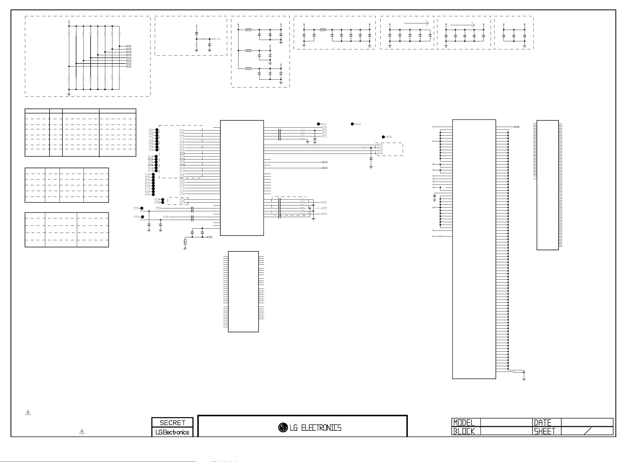
MODEL OPTION
Copyright ⓒ 2015 LG Electronics. Inc. All right reserved.
Only for training and service purposes
LGE Internal Use Only
+3.3V_Normal
1K
MO_DUALSTREAM
R290
1K
R293
MO_DUALSTREAM_NON
DDR_EXT:256
MO_S/W_EU/AJ
R291 1K
R222 1K
R221 1K
MO_S/W_TW/CN
R294 1K
DDR_EXT:128 or NON
R224 1K
R223 1K
MO_M120
DDR_EXT:128
R206 1K
R208 1K
MO_DVB_T2/C/S2
MO_DVB_T/C
MO_M120_NON
DDR_EXT:256 or NON
R207 1K
R209 1K
MO_HD
MO_S/W_AJ
R226 1K
R211 1K
MO_FHD
MO_S/W_NON_AJ
R212 1K
R227 1K
MODEL_OPT_0
MODEL_OPT_1
MODEL_OPT_2
AUD_LRCH
MODEL_OPT_4
MODEL_OPT_5
MODEL_OPT_6
AUD_LRCK
SOC_RESET
+3.5V_ST
C200
4.7uF
10V
R200
470K
R217
0
C201
0.1uF
STby 3.5V
+3.5V_ST
L206
BLM18PG121SN1D
C289
SOC_RESET
16V
10uF
10V
L207
BLM18PG121SN1D
C288
10uF
10V
L208
BLM18PG121SN1D
C240
0.1uF
16V
C286
0.1uF
16V
AVDD_DMPLL
C205
0.1uF
16V
C287
10uF
10V
AVDD_NODIE
C252
0.1uF
16V
AVDD_AU33
C241
0.1uF
16V
Normal Power 3.3V
L204
BLM18PG121SN1D
C255
C259
0.1uF
0.1uF
16V
16V
C284
10uF
10V
C204
10uF
10V
C209
0.1uF
16V
C235
0.1uF
16V
C245
0.1uF
16V
VDD33
DDR3 1.5V
+1.5V_DDR+3.3V_Normal
C278 C248
C266
10uF
0.1uF
10V
16V
AVDD_DDR1:55mA
AVDD_DDR0:55mA
0.1uF
0.1uF
16V
C207
VDDC 1.05V
+1.10V_VDDC
+1.10V_VDDC+1.10V_VDDC
+1.10V_VDDC
VDDC : 2026mA
C254
16V
C228
1uF
10uF
10V
10V
C275
10uF
C277
1uF
10V
10V
C280
1uF
10V
C283
0.1uF
C210
0.1uF
C279
0.1uF
16V
16V
C296
16V
10uF
10V
MODEL OPTION
PIN NAME
MODEL_OPT_0
MODEL_OPT_1
MODEL_OPT_2
AUD_LRCH
MODEL_OPT_4
MODEL_OPT_5
MODEL_OPT_6
AUD_LRCK
* Dual Stream is only Korea 3D spec
Memory OPTION
Memory
INT+EXT
128M Only
256M Only
128M+128M
PIN NO.
H19
G20
G19
Auto
Det
0
1
0
0128M+256M
J5
MO_FHD
MO_S/W_NON_AJ
MO_DVB_T/C
MO_M120_NON
LOW
DDR_EXT:256 or NON DDR_EXT : 128
U6
K5
MO_S/W_TW/CN
K4
L5
MODEL_OPT_4
0
0
1
0
Country Option
MODEL_OPT_1
TW
EU
CN
0
0
1
1
MODEL_OPT_6
0
0
0
1
101256M+256M
MODEL_OPT_5
0
1
0
1AJ
HIGH
MO_HD
MO_S/W_AJ
MO_DVB_T2/C/S2
MO_M120
MO_S/W_EU/AJ
DDR_EXT : 256DDR_EXT:128 or NON
MO_DUALSTREAMMO_DUALSTREAM_NON
AV2_L_IN
COMP2_L_IN
AV2_R_IN
COMP2_R_IN
D0-_HDMI4
D0+_HDMI4
D1-_HDMI4
D1+_HDMI4
D2-_HDMI4
D2+_HDMI4
CK-_HDMI4
CK+_HDMI4
DDC_SCL_2
DDC_SDA_2
DDC_SCL_4
DDC_SDA_4
HPD2
HPD4
D0-_HDMI2
D0+_HDMI2
D1-_HDMI2
D1+_HDMI2
D2-_HDMI2
D2+_HDMI2
CK-_HDMI2
CK+_HDMI2
1000pF
C211
OPT
50V
HP_LOUT
HP_ROUT
AV2_L_IN
AV2_R_IN
OPT
C215
1000pF
50V
HDMI
D0-_HDMI4
D0+_HDMI4
D1-_HDMI4
D1+_HDMI4
D2-_HDMI4
D2+_HDMI4
CK-_HDMI4
CK+_HDMI4
CEC_REMOTE_S7
DDC_SCL_2
DDC_SDA_2
DDC_SCL_4
DDC_SDA_4
HPD2
HPD4
D0-_HDMI2
D0+_HDMI2
D1-_HDMI2
D1+_HDMI2
D2-_HDMI2
D2+_HDMI2
CK-_HDMI2
CK+_HDMI2
BLM18PG121SN1D
HP_LOUT
HP_ROUT
L214
H/P OUT
2.2uF
C218
C216 2.2uF
C246 2.2uF
C219 2.2uF
C213
C220
1uF
4.7uF
AV2
NON_EU
AV2
NON_EU
AA9
AA7
AA6
AUVRM
M4
W7
Y8
W8
Y9
W9
Y7
N2
E3
E2
W6
L4
Y6
F1
G3
G1
G2
H3
H2
F3
F2
U4
T4
P2
R2
T1
R3
R1
T3
U2
V3
T2
M1A_256M_UO4
IC101
LGE2134(256M)
ARC0
RXC0N
RXC0P
RXC1N
RXC1P
RXC2N
RXC2P
I2S_OUT_BCK/GPIO165
RXCCKN
I2S_OUT_MCK/GPIO163
RXCCKP
CEC/GPIO6
DDCDA_CK/GPIO27
DDCDA_DA/GPIO28
DDCDC_CK/GPIO31
DDCDC_DA/GPIO32
HOTPLUGA/GPIO23
HOTPLUGC/GPIO25
RXA0N
RXA0P
RXA1N
RXA1P
RXA2N
RXA2P
RXACKN
RXACKP
EAR_OUTL
EAR_OUTR
AUL1
AUL2
AUL3
AUR1
AUR2
AUR3
AUOUTL0
AUOUTR0
AUVAG
M4
W7
Y8
W8
Y9
AA9
W9
AA7
Y7
N2
E3
E2
W6
AA6
L4
Y6
F1
G3
G1
G2
H3
H2
F3
F2
U4
T4
P2
R2
T1
R3
R1
T3
U2
V3
T2
M1A_128M_UO4
IC101-*1
LGE2133(128M)
ARC0
RXC0N
RXC0P
RXC1N
RXC1P
RXC2N
RXC2P
RXCCKN
RXCCKP
CEC/GPIO6
DDCDA_CK/GPIO27
DDCDA_DA/GPIO28
DDCDC_CK/GPIO31
DDCDC_DA/GPIO32
HOTPLUGA/GPIO23
HOTPLUGC/GPIO25
RXA0N
RXA0P
RXA1N
RXA1P
RXA2N
RXA2P
RXACKN
RXACKP
EAR_OUTL
EAR_OUTR
AUL1
AUL2
AUL3
AUR1
AUR2
AUR3
AUOUTL0
AUOUTR0
AUVAG
I2S_OUT_SD/GPIO166
I2S_OUT_WS/GPIO164
CVBSOUT1
CVBSOUT1
I2S_OUT_BCK/GPIO165
I2S_OUT_MCK/GPIO163
I2S_OUT_SD/GPIO166
I2S_OUT_WS/GPIO164
USB0_DM
USB1_DM
USB0_DP
USB1_DP
HSYNC0
VSYNC0
SOGIN1
CVBS0
CVBS1
CVBS2
VCOM
USB0_DM
USB1_DM
USB0_DP
USB1_DP
BIN0M
BIN0P
GIN0M
GIN0P
RIN0M
RIN0P
HSYNC0
VSYNC0
BIN1M
BIN1P
GIN1M
GIN1P
RIN1M
RIN1P
SOGIN1
CVBS0
CVBS1
CVBS2
VCOM
BIN0M
BIN0P
GIN0M
GIN0P
RIN0M
RIN0P
BIN1M
BIN1P
GIN1M
GIN1P
RIN1M
RIN1P
T6
V5
U5
T5
V4
E4
F4
F7
F5
C4
Y12
B4
AA12
J2
J3
K3
J1
K2
K1
M6
L6
L2
L3
M1
M2
N1
N3
M3
T6
V5
U5
T5
V4
E4
F4
F7
F5
C4
Y12
B4
AA12
J2
J3
K3
J1
K2
K1
M6
L6
L2
L3
M1
M2
N1
N3
M3
C227 0.047uF
C229 0.047uF
C231 0.047uF
C232 0.047uF
C233 0.047uF
C234 1000pF
Close to MSTAR
C2360.047uF
CVBS
C2370.047uF
EU_AV2
C2380.047uF
NON_EU
*CAPTION OPT:NON_EU
NON_EU
R238 68
R239 33
R240 68C230 0.047uF
R241 33
R242 68
R243 33
M1A_256M_UO4
IC101
LGE2134(256M)
DTV/MNT_VOUT
OPT
C242
1000pF
50V
DTV/MNT_VOUT
TU_CVBS
SC1/AV2_CVBS_IN
COMP2_Y+/AV_CVBS_IN
R24433
CVBS
R24533
EU_AV2
R24633
NON_EU
R24768C2390.047uF
SIDE_USB1_DM
SIDE_USB1_DP
COMP2_Pb+
COMP2_Y+/AV_CVBS_IN
COMP2_Pr+
SC1/AV2_CVBS_IN
R295 0
OPT
OPT
C208
15pF
50V
I2S_I/F
AUD_MASTER_CLK
AUD_SCK
AUD_MASTER_CLK
AUD_LRCH
AUD_LRCK
AVDD_AU33
+1.5V_DDR
AVDD_NODIE
VDD33
AVDD_NODIE
VDD33
AVDD_DMPLL
+1.10V_VDDC
+1.10V_VDDC
+1.10V_VDDC
VDD33
5V_HDMI_4
C260
1uF
10V
OPT
R296
10
5%
R4
AVDD_AU33
L11
AVDD_DDR0_CLK
L13
AVDD_DDR1_CLK
M11
AVDD_DDR0_CMD
K13
AVDD_DDR1_CMD
C5
AVDD_DDR0_D_1
K12
AVDD_DDR0_D_2
L12
AVDD_DDR0_D_3
C6
AVDD_DDR1_D_1
K14
AVDD_DDR1_D_2
L14
AVDD_DDR1_D_3
B5
AVDD_DRAM_1
B6
AVDD_DRAM_2
R8
AVDD_DVI_USB_MPLL_1
R9
AVDD_DVI_USB_MPLL_2
L7
AVDD_MOD_1
L8
AVDD_MOD_2
P8
AVDD_NODIE
K9
AVDD_PLL
R5
AVDD3P3_DMPLL
P11
AVDDL_MOD
C7
DVDD_DDR_1
M13
DVDD_DDR_2
R6
DVDD_NODIE
A7
DVDD_RX_1_1
M12
DVDD_RX_1_2
B7
DVDD_RX_2_1
M14
DVDD_RX_2_2
N11
VDDC_1
N12
VDDC_2
N13
VDDC_3
N14
VDDC_4
N15
VDDC_5
P12
VDDC_6
P13
VDDC_7
P14
VDDC_8
L9
VDDP
AA10
AVDD5V_MHL
AUVRM
GND_1
GND_2
GND_3
GND_4
GND_5
GND_6
GND_7
GND_8
GND_9
GND_10
GND_11
GND_12
GND_13
GND_14
GND_15
GND_16
GND_17
GND_18
GND_19
GND_20
GND_21
GND_22
GND_23
GND_24
GND_25
GND_26
GND_27
GND_28
GND_29
GND_30
GND_31
GND_32
GND_33
GND_34
GND_35
GND_36
GND_37
GND_38
GND_39
GND_40
GND_41
GND_42
GND_43
GND_44
GND_45
GND_46
GND_47
GND_48
GND_49
GND_50
GND_51
GND_52
GND_53
GND_54
GND_55
GND_56
GND_57
GND_58
GND_59
GND_60
GND_61
GND_62
GND_63
GND_64
GND_65
GND_66
GND_67
GND_68
GND_69
GND_70
GND_71
GND_72
GND_73
GND_74
GND_75
GND_76
GND_77
GND_78
GND_79
GND_80
GND_81
GND_82
GND_83
GND_84
GND_EFUSE
U3
A6
A13
A15
A18
B12
B14
B16
B17
B19
B20
C9
C10
C21
D9
E20
F9
F11
F13
F15
F17
F19
F21
G8
G9
G10
G11
G12
G13
G14
G15
G16
G17
G18
H7
H8
H9
H10
H11
H12
H13
H14
H15
H16
H17
H18
J7
J8
J9
J10
J11
J12
J13
J14
K8
K10
K11
L10
M5
M7
M8
M9
M10
N4
N5
N6
N7
N8
N9
N10
P4
P5
P6
P7
P9
P10
P15
P16
P17
P18
R10
R11
R12
R13
R14
K7
AUVRM
R4
AVDD_AU33
L11
AVDD_DDR0_CLK
L13
AVDD_DDR1_CLK
M11
AVDD_DDR0_CMD
K13
AVDD_DDR1_CMD
C5
AVDD_DDR0_D_1
K12
AVDD_DDR0_D_2
L12
AVDD_DDR0_D_3
C6
AVDD_DDR1_D_1
K14
AVDD_DDR1_D_2
L14
AVDD_DDR1_D_3
B5
AVDD_DRAM_1
B6
AVDD_DRAM_2
R8
AVDD_DVI_USB_MPLL_1
R9
AVDD_DVI_USB_MPLL_2
L7
AVDD_MOD_1
L8
AVDD_MOD_2
P8
AVDD_NODIE
K9
AVDD_PLL
R5
AVDD3P3_DMPLL
P11
AVDDL_MOD
C7
DVDD_DDR_1
M13
DVDD_DDR_2
R6
DVDD_NODIE
A7
DVDD_RX_1_1
M12
DVDD_RX_1_2
B7
DVDD_RX_2_1
M14
DVDD_RX_2_2
N11
VDDC_1
N12
VDDC_2
N13
VDDC_3
N14
VDDC_4
N15
VDDC_5
P12
VDDC_6
P13
VDDC_7
P14
VDDC_8
L9
VDDP
AA10
AVDD5V_MHL
M1A_128M_UO4
IC101-*1
LGE2133(128M)
GND_EFUSE
U3
AUVRM
A6
GND_1
A13
GND_2
A15
GND_3
A18
GND_4
B12
GND_5
B14
GND_6
B16
GND_7
B17
GND_8
B19
GND_9
B20
GND_10
C9
GND_11
C10
GND_12
C21
GND_13
D9
GND_14
E20
GND_15
F9
GND_16
F11
GND_17
F13
GND_18
F15
GND_19
F17
GND_20
F19
GND_21
F21
GND_22
G8
GND_23
G9
GND_24
G10
GND_25
G11
GND_26
G12
GND_27
G13
GND_28
G14
GND_29
G15
GND_30
G16
GND_31
G17
GND_32
G18
GND_33
H7
GND_34
H8
GND_35
H9
GND_36
H10
GND_37
H11
GND_38
H12
GND_39
H13
GND_40
H14
GND_41
H15
GND_42
H16
GND_43
H17
GND_44
H18
GND_45
J7
GND_46
J8
GND_47
J9
GND_48
J10
GND_49
J11
GND_50
J12
GND_51
J13
GND_52
J14
GND_53
K8
GND_54
K10
GND_55
K11
GND_56
L10
GND_57
M5
GND_58
M7
GND_59
M8
GND_60
M9
GND_61
M10
GND_62
N4
GND_63
N5
GND_64
N6
GND_65
N7
GND_66
N8
GND_67
N9
GND_68
N10
GND_69
P4
GND_70
P5
GND_71
P6
GND_72
P7
GND_73
P9
GND_74
P10
GND_75
P15
GND_76
P16
GND_77
P17
GND_78
P18
GND_79
R10
GND_80
R11
GND_81
R12
GND_82
R13
GND_83
R14
GND_84
K7
THE SYMBOL MARK OF THIS SCHEMETIC DIAGRAM INCORPORATES
SPECIAL FEATURES IMPORTANT FOR PROTECTION FROM X-RADIATION.
FIRE AND ELECTRICAL SHOCK HAZARDS, WHEN SERVICING IF IS
ESSENTIAL THAT ONLY MANUFACTURES SPECIFIED PARTS BE USED FOR
THE CRITICAL COMPONENTS IN THE SYMBOL MARK OF THE SCHEMETIC.
L15.5_CI_M1A
MAIN2_DVB
150511
2
Page 31
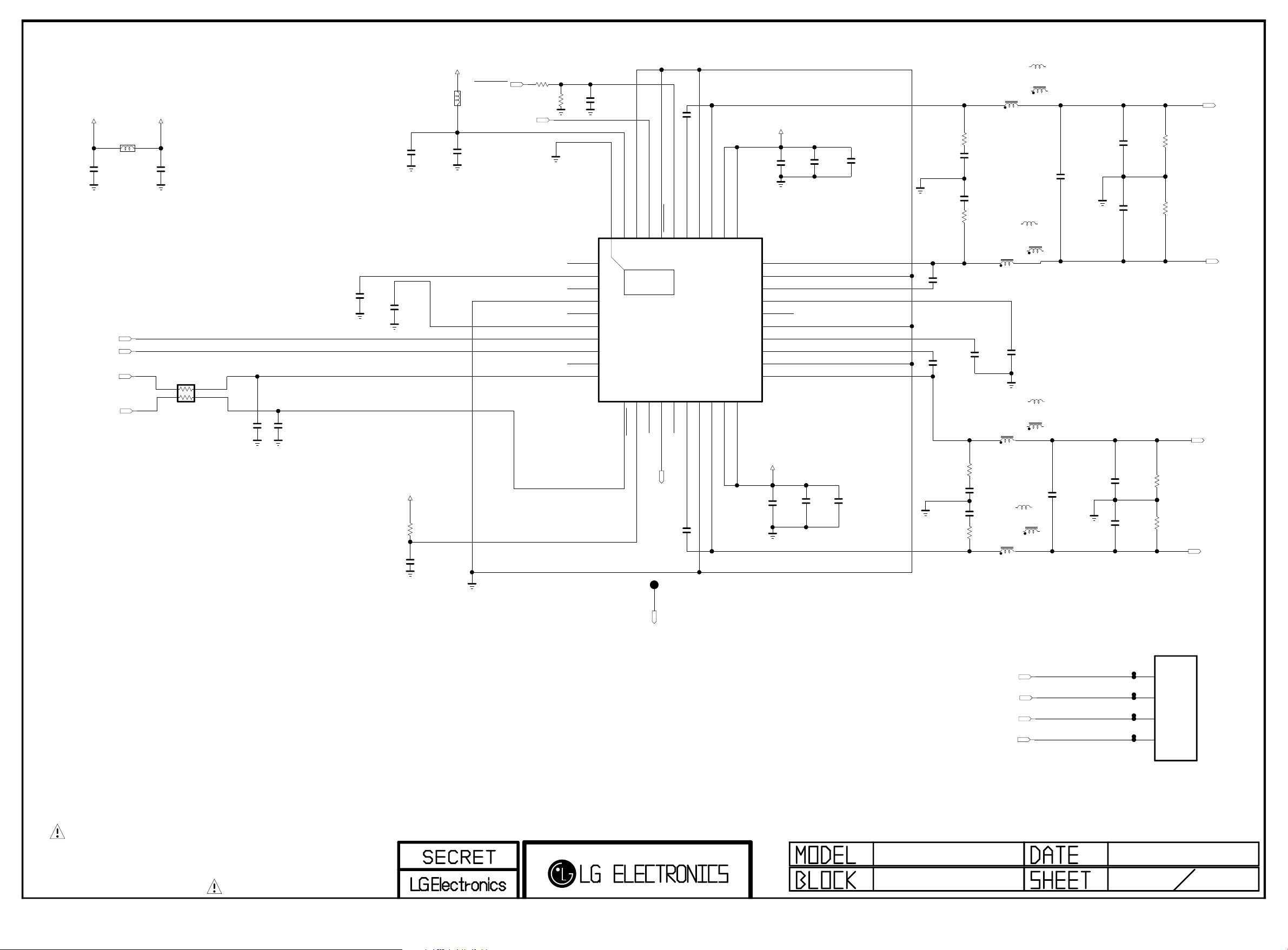
AUDIO AMP(NTP7515)
Copyright ⓒ 2015 LG Electronics. Inc. All right reserved.
Only for training and service purposes
LGE Internal Use Only
+19V
UBW2012-121F
OPT
C5600
0.1uF
50V
AUD_LRCH
AUD_LRCK
AMP_SDA
AMP_SCL
L5600
+19V_AMP
C5601
0.1uF
50V
AR5601
100
1/16W
C5602
33pF
50V
C5603
33pF
50V
C5604
1uF
10V
BLM18PG121SN1D
C5607
10uF
10V
C5605
1uF
10V
+3.3V_Normal
OPT
C5606
1000pF
50V
R5603
10K
L5601
+3.3V_Normal
C5608
0.1uF
16V
AMP_RESET
AUD_SCK
R5606
100
1/16W
R5607
4.7K
NC_1
VDD_PLL
NC_2
GND
NC_3
DVDD
SDATA
WCK
NC_4
SDA
C5609
1000pF
50V
[EP]GND
1
2
3
4
5
6
7
8
9
10
GND_IO
VDD_IO
39
40
THERMAL
41
11
12
SCL
FAULT
50V
C5610
BST1A
RESET
AD
CLK_I
35
36
37
38
IC5600
NTP7515
13
14
15
16
BST2B
MONITOR_0
MONITOR_1
MONITOR_2
I2S_AMP
C5611
22000pF
50V
22000pF
OUT1A
PGND1A
33
34
17
18
OUT2B
PGND2B
PVDD1B
PVDD1A
31
32
30
29
28
27
26
25
24
23
22
21
19
PVDD2B20PVDD2A
+19V_AMP
+19V_AMP
C5613
10uF
25V
OUT1B
PGND1B
BST1B
VDR1
NC_5
AGND
VDR2
BST2A
PGND2A
OUT2A
C5612
10uF
25V
C5615
0.1uF
50V
C5614
0.1uF
50V
C5616
4.7uF
50V
3216
C5617
4.7uF
50V
3216
OPT
OPT
C5618
22000pF
50V
C5619
22000pF
50V
R5608
3.3
R5609
3.3
R5610
R5611
3.3
3.3
1/10W
5%
C5620
390pF
50V
C5621
390pF
50V
1/10W
5%
C5624
1uF
10V
1/10W
C5622
390pF
50V
C5623
390pF
50V
1/10W
TAIYO
L5603-*2
10.0uH
CYNTEC
L5603-*1
10uH
TDK
L5603
10uH
C5630
0.1uF
50V
C5627
0.47uF
50V
TAIYO
L5605-*2
10.0uH
CYNTEC
L5605-*1
TDK
10uH
L5605
10uH
C5625
1uF
10V
TAIYO
L5602-*2
10.0uH
CYNTEC
L5602-*1
10uH
TDK
L5602
10uH
5%
TAIYO
L5604-*2
10.0uH
CYNTEC
L5604-*1
10uH
TDK
L5604
5%
10uH
C5626
0.47uF
50V
C5631
0.1uF
C5628
0.1uF
50V
C5629
0.1uF
50V
50V
R5614
4.7K
R5615
4.7K
R5612
4.7K
R5613
4.7K
SPK_L+
SPEAKER_L
SPK_L-
SPK_R+
SPEAKER_R
SPK_R-
THE SYMBOL MARK OF THIS SCHEMETIC DIAGRAM INCORPORATES
SPECIAL FEATURES IMPORTANT FOR PROTECTION FROM X-RADIATION.
FIRE AND ELECTRICAL SHOCK HAZARDS, WHEN SERVICING IF IS
ESSENTIAL THAT ONLY MANUFACTURES SPECIFIED PARTS BE USED FOR
THE CRITICAL COMPONENTS IN THE SYMBOL MARK OF THE SCHEMETIC.
I2S_AMP
L15.5_ECI_M1A
AMP_NTP
SPK_L+
SPK_L-
SPK_R+
SPK_R-
250A1-WR-H04M
WAFER-ANGLE
4
3
2
1
P5600
Box Type SPK Wafer
150112
56
Page 32
Page 33

Trouble shooting guide
Copyright © 2015 LG Electronics. Inc. All rights reserved.
Only for training and service purposes
LGE Internal Use Only
Page 34
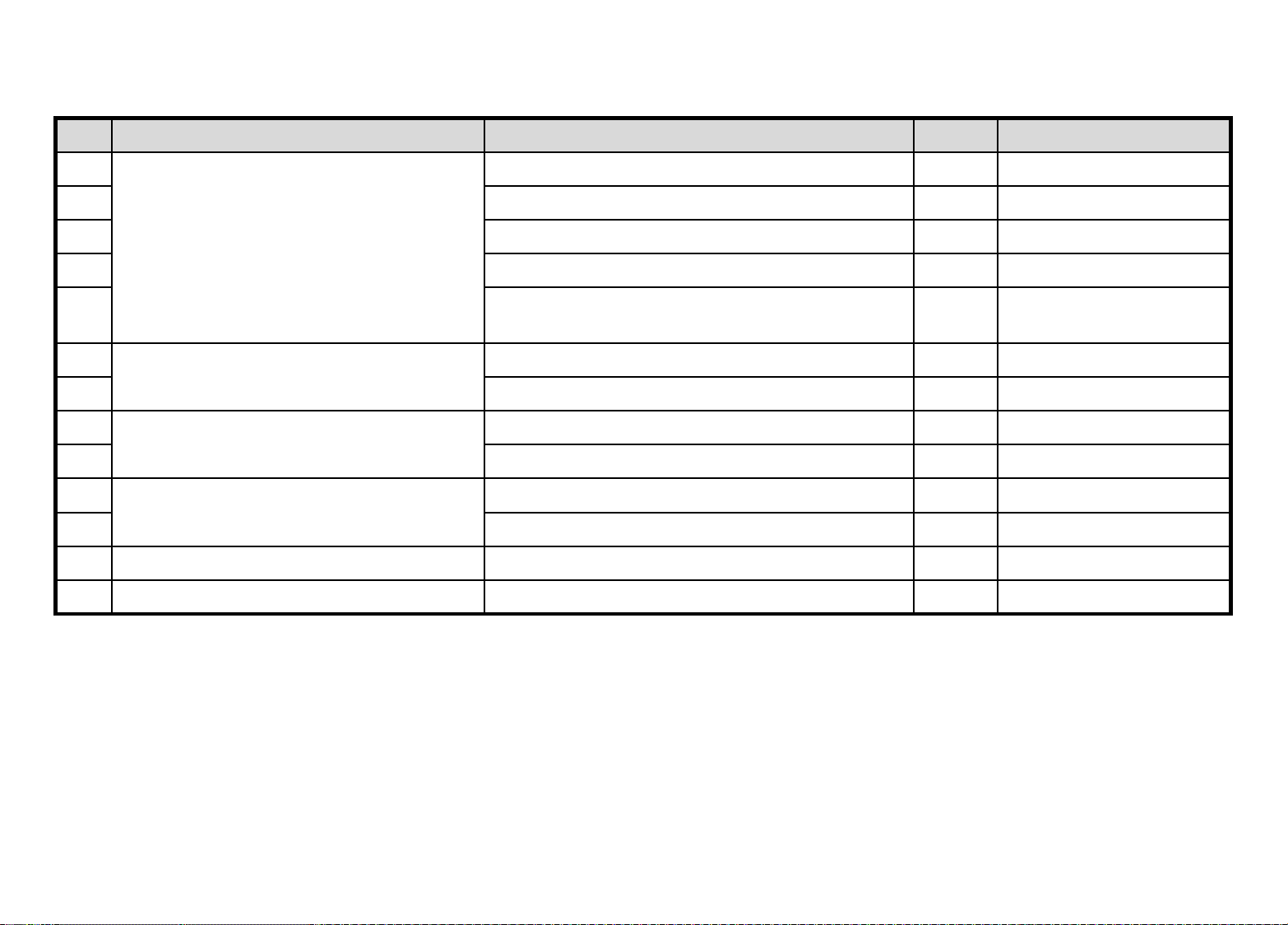
No. Error symptom (High category) Error symptom (Mid category) Page Remarks
1
A. Video error
No video/Normal audio 1
2 No video/No audio 2
3 Tuning fail, Picture broken/ Freezing 3, 4
4 Color error 5
5
Vertical/Horizontal bar, residual image, light spot,
external device color error
6
6
B. Power error
No power 7
7 Off when on, off while viewing, power auto on/off 8
8
C. Audio error
No audio/Normal video 9
9 Wrecked audio/discontinuation/noise 10
10
D. Function error
Remote control & Local switch checking 11
11 External device recognition error 12
12 E. Noise Circuit noise, mechanical noise 13
13 F. Exterior error Exterior defect 14
* First of all, Check whether there is SVC Bulletin in GCSC System for these model.
Contents of Standard Repair Process
Copyright © 2015 LG Electronics. Inc. All rights reserved.
Only for training and service purposes
LGE Internal Use Only
Page 35
Y
N
Move to
No video/No audio
No video
Normal audio
Check Back Light
On with naked eye
Check LVDS 12 V
of Main B/D
Replace T-con B/D
or Module
Replace Main
B/D or Repair parts
Check Main B/D to LED Back light Voltage
Replace Module
Replace Main
B/D or Repair parts
Always check & record S/W Version and White
Balance value before replacing the Main Board
Replace Main Board Re-enter White Balance value
※Precaution
☞A4 ☞A1
☞A2
☞A3 & A6
First of all, Check whether all of cables between board is inserted properly or not.
(Main B/D ↔ Adaptor, LVDS Cable, Speaker Cable, IR B/D Cable…)
Normal
Audio
On
Y
N
Normal
Voltage
Normal
Voltage
Y
N
Y
N
Error Symptom
A. Video Error
Established date
2015.04.17
1/14
Content
No video / Normal audio
Revised date
Standard Repair Process
Copyright © 2015 LG Electronics. Inc. All rights reserved.
Only for training and service purposes
LGE Internal Use Only
Page 36
Check voltage 19V
of Adaptor
No video /
No audio
Replace Main
B/D or Repair parts
Replace Adaptor
Normal
Voltage
Y
N
Error Symptom
A. Video Error
Established date
2015.04.17
2/14
Content
No video / No audio
Revised date
Standard Repair Process
☞A13
Copyright © 2015 LG Electronics. Inc. All rights reserved.
Only for training and service purposes
LGE Internal Use Only
Page 37
Y
N
☞ A5
N
Check RF Signal level
Check RF Cable
Connection
1. Reconnection
2. Install Booster
Check
S/W Version
S/W Upgrade
Check whether other equipments have problem or not.
(By connecting RF Cable at other equipment)
→ DVD Player ,Set-Top-Box, Different maker TV etc`
Replace
Main B/D
Check
Tuner soldering
Y
N
Y
Y
. By using Digital signal level meter
. By using Diagnostics menu on OSD
( Menu → Customer Support(red button on remote control) → Signal Test )
- Signal strength (Normal : over 50%)
- Signal quality (Normal : over 50%)
Y
Contact with signal distributor
or broadcaster (Cable or Air)
N
N
Y
N
☞ A6
End
Normal
Signal
Normal
Picture
Normal
Picture
Normal
Picture
SVC
Bulletin
End
End
Normal
Picture
Error Symptom
A. Video Error
Established date
2015.04.17
3/14
Content
Tuning fail, Picture broken/freezing
Revised date
Standard Repair Process
Copyright © 2015 LG Electronics. Inc. All rights reserved.
Only for training and service purposes
LGE Internal Use Only
Page 38
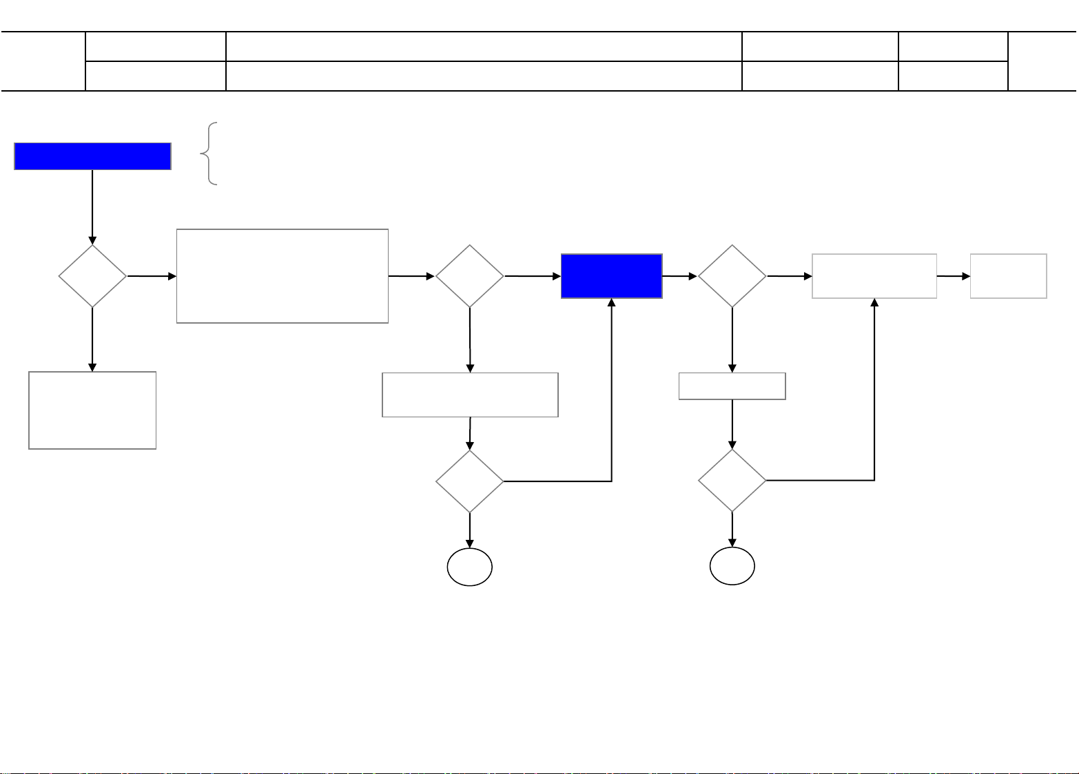
Y
N
☞ A5
Check RF Signal level
Check
S/W Version
S/W Upgrade
Y
N
Y
Check RF signal cable (DVB satellite signal or not)
Check whether other equipments have problem or not.
(By connecting RF Cable at other equipment)
→ Set-Top-Box, Different maker TV etc
Y
Replace satellite setting
(match with installed ANT)
N
Y
N
☞ A6
Check satellite setting.
- Check LNB frequency
- Check satellite
- Check Satellite connection
(DiSEqC, motor, etc…)
Contact with signal
distributor
or broadcaster
(Cable or Air)
N
Check
Tuner soldering
Replace
Main B/D
Normal
Picture
Normal
Picture
Normal
Setting
SVC
Bulletin
Normal
Signal
End
End
Error Symptom
A. Video Error
Established date
2015.04.17
4/14
Content
Tuning fail, Picture broken/freezing
Revised date
Standard Repair Process
Copyright © 2015 LG Electronics. Inc. All rights reserved.
Only for training and service purposes
LGE Internal Use Only
Page 39
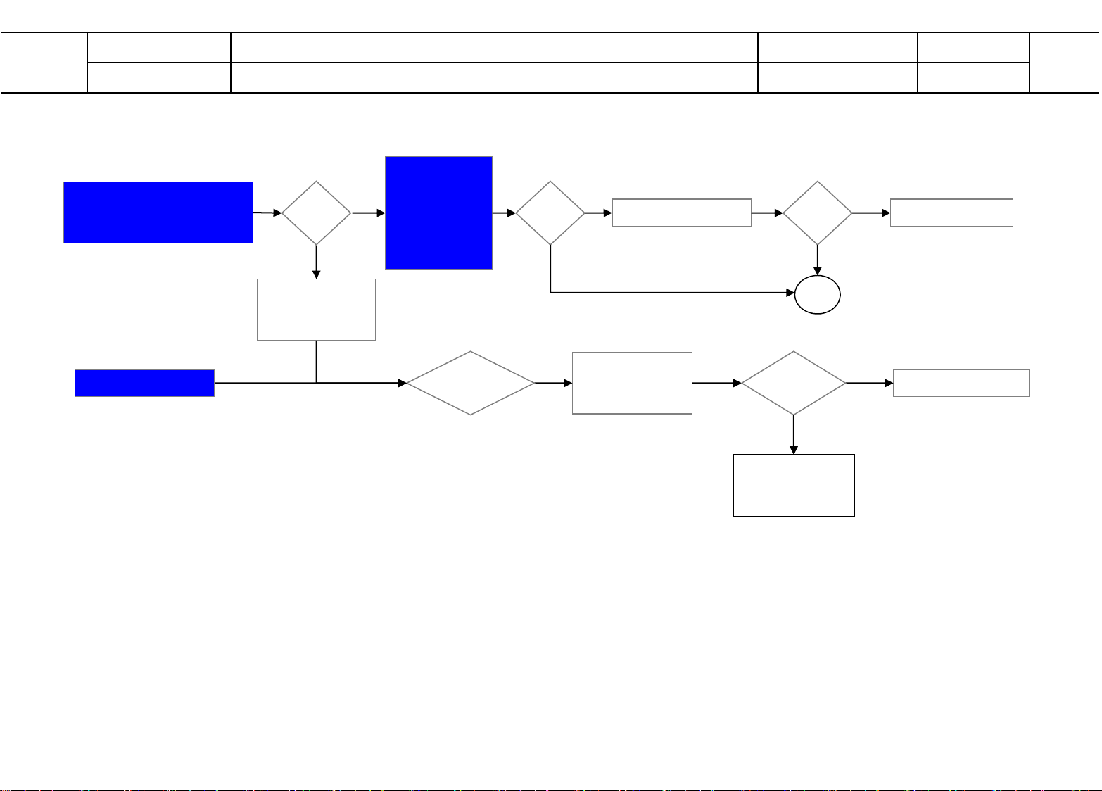
Color
error
Y
N
Check and
replace Link
Cable
(LVDS) and
contact
condition
Y
N
Replace Main B/D
Check error
color input
mode
Check color by input
- External Input
(COMPONENT/AV/HDMI)
Y
Check external
device and
cable
Replace Main B/D
N
☞A7
N
Y
Replace module
Request repair
for external
device/cable
Check Test pattern
☞A10
☞ A8 / A9
End
Color
error
Color
error
External
device/Cable
Normal
External
Input Component,
HDMI error
Error Symptom
A. Video Error
Established date
2015.04.17
5/14
Content
Color error
Revised date
Standard Repair Process
Copyright © 2015 LG Electronics. Inc. All rights reserved.
Only for training and service purposes
LGE Internal Use Only
Page 40
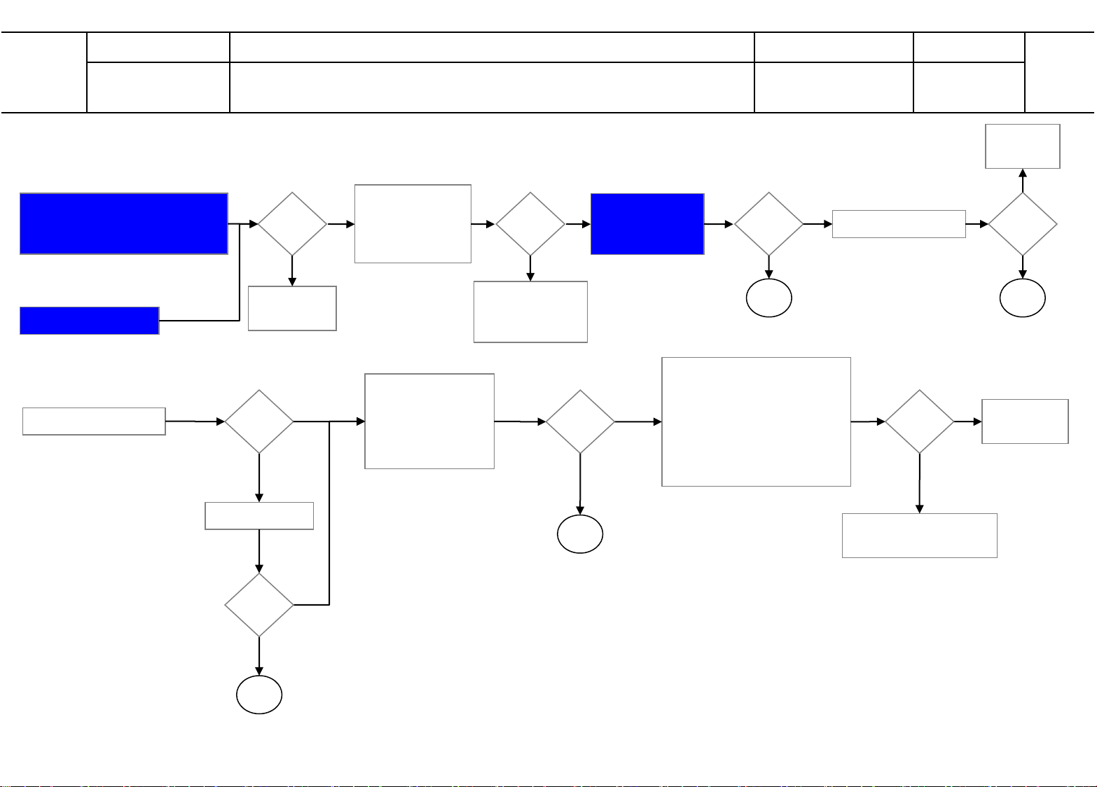
N
Y
Check external
device
connection
condition
Y
N
Check and
replace Link
Cable
Y
Replace
Module
Check color condition by input
- External Input
(Component/AV/HDMI)
Vertical/Horizontal bar, residual image, light spot
Request repair
for external
device
☞A10
External device screen error-Color error
Connect other external
device and cable
(Check normal operation of
External Input, Component
and HDMI by connecting
Jig, pattern Generator,
Set-top Box etc.
N
Y
Replace
Main B/D
Check screen
condition by input
-External Input
(Component/AV/
HDMI)
Request repair for
external device
Check S/W Version
Y
N
S/W Upgrade
Y
N
Y
N
Replace Main B/D
Replace
Module
☞A7
☞ A8/ A9
Check Test pattern
N
End
Screen
normal
Screen
normal
Screen
normal
Screen
normal
Screen
normal
End
End
Check
Version
Normal
Screen
External
Input
error
Error Symptom
A. Video Error
Established date
2015.04.17
6/14
Content
Vertical/Horizontal bar, Residual Image,
Light spot, External device Color error
Revised date
Standard Repair Process
Y
N
End
Copyright © 2015 LG Electronics. Inc. All rights reserved.
Only for training and service purposes
LGE Internal Use Only
Page 41
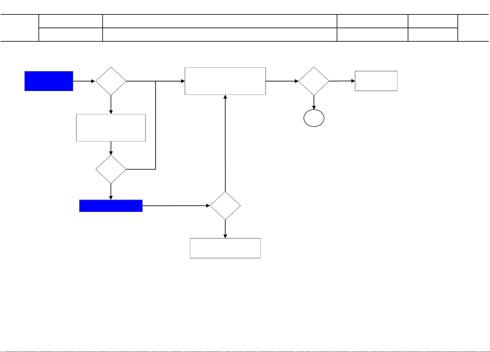
Power
LED On
Y
N
DC Power on
by pressing Power Key
On Remote control
Y
N
Check Adaptor/
Power cord
was inserted properly
Check
Power LED
Replace
Main B/D
N
Y
Check ST-BY 3.5V
N
Replace Adaptor or
Replace Main B/D
Y
☞A11
☞A16
Stand-By : Red
※
Power
LED On
Normal
Voltage
Normal
Operation
Error Symptom
B. Power Error
Established date
2015.04.17
7/14
Content
No power
Revised date
Standard Repair Process
End
Copyright © 2015 LG Electronics. Inc. All rights reserved.
Only for training and service purposes
LGE Internal Use Only
Page 42
Normal
Voltage
N
Y
Check Power Off
Mode
Fix A/C cord & Outlet
Replace Main B/D
(If Power Off mode
is not displayed)
Check Adaptor
voltage
Y
N
Replace Main B/D
Replace Adaptor
Replace Adaptor
N
Y
☞A14
☞A13
Status Power off List Explanation
Normal
"POWEROFF_REMOTEKEY" Power off by REMOTE CONTROL
"POWEROFF_OFFTIMER" Power off by OFF TIMER
"POWEROFF_SLEEPTIMER" Power off by SLEEP TIMER
"POWEROFF_INSTOP" Power off by INSTOP KEY
"POWEROFF_AUTOOFF" Power off by AUTO OFF
"POWEROFF_ONTIMER" Power off by ON TIMER
"POWEROFF_RS232C" Power off by RS232C
"POWEROFF_RESREC" Power off by Reservated Record
"POWEROFF_RECEND" Power off by End of Recording
"POWEROFF_SWDOWN" Power off by S/W Download
"POWEROFF_UNKNOWN" Power off by unknown status except listed case
Abnormal
"POWEROFF_ABNORMAL1" Power off by abnormal status except CPU trouble
"POWEROFF_CPUABNORMAL" Power off by CPU Abnormal
* Please refer to the all cases which
can be displayed on power off mode.
Adaptor
DC Out
CPU
Abnorm
al
Abnorm
al1
Normal End
Error Symptom
B. Power Error
Established date
2015.04.17
8/14
Content
Off when on/off while viewing, power auto on/off
Revised date
Standard Repair Process
Replace
Adaptor
Y
Error
N
Check outlet
or A/C cord
Copyright © 2015 LG Electronics. Inc. All rights reserved.
Only for training and service purposes
LGE Internal Use Only
Page 43
No audio
Screen normal
Check user
Connection
from Main
Speaker Cable
N
Y
Insert wafer SPK Cable
Replace Speaker
or Main B/D
Connec
tion
Error Symptom
C. Audio Error
Established date
2015.04.17
9/14
Content
No audio / Normal video
Revised date
Standard Repair Process
☞A15
Normal
Audio
End
Y
N
Copyright © 2015 LG Electronics. Inc. All rights reserved.
Only for training and service purposes
LGE Internal Use Only
Page 44
Check and replace
speaker and
connector
Connect and check
other external
device
Y
Check and fix external device
Replace Adaptor
N
Y
Check input
signal
-RF
-External Input
(When RF signal is not received)
Request repair to external
cable/ANT provider
Y
Check Voltage 19V
of Adaptor
(In case of External Input
signal error)
Check and fix external device
Replace Main B/D
N
☞A13
End
Signal
Normal
Normal
Voltage
Normal
Audio
Wrecked Audio/
Discontinuation/Noise
for all audio
Wrecked Audio/
Discontinuation/Noise
only for D-TV
Wrecked Audio/
Discontinuation/Noise
only for Analog
Wrecked Audio/
Discontinuation/Noise
only for External Input
N
Replace Main B/D
Error Symptom
C. Audio Error
Established date
2015.04.17
10/14
Content
Wrecked audio / Discontinuation / Noise
Revised date
Standard Repair Process
Copyright © 2015 LG Electronics. Inc. All rights reserved.
Only for training and service purposes
LGE Internal Use Only
Page 45
Y
N
Check R/C itself
Operation
Y
Replace R/C
If R/C operate,
Explain the customer
cause is interference
from light in room.
Check R/C Operating
When turn off light
in room
Check & Replace
Baterry of R/C
Check & Repair
Cable connection
Connector solder
Check 3.5V
On Main B/D
☞A16
N
N
Check Voltage 19V of Adaptor
☞A13
Check IR
Output signal
N
Y
Replace
IR B/D
N
☞A16
Replace
Main B/D
Y
☞A16
End
Normal
Operating
Normal
Voltage
Normal
Signal
Normal
Operating
Normal
Operating
End
Y
Error Symptom
D. Function Error
Established date
2015.04.17
11/14
Content
Remote control & Local switch checking
Revised date
Standard Repair Process
Copyright © 2015 LG Electronics. Inc. All rights reserved.
Only for training and service purposes
LGE Internal Use Only
Page 46
Check technical
information
- Fix information
- S/W Version
N
Y
Check input
signal
Y
N
Check and fix
external device/cable
Replace Main B/D
Fix in
accordance
with technical
information
Signal
Input
Technical
information
External Input
and Component
Recognition error
HDMI
Recognition
error
Error Symptom
D. Function Error
Established date
2015.04.17
12/14
Content
External device recognition error
Revised date
Standard Repair Process
Copyright © 2015 LG Electronics. Inc. All rights reserved.
Only for training and service purposes
LGE Internal Use Only
Page 47
Check location
of noise
Identify
nose type
Replace Main Board
Check location
of noise
※ When the nose is severe, replace the module
(For models with fix information, upgrade the S/W or
provide the description)
※ If there is a “Tak Tak” noise from the cabinet, refer
to the KMS fix information and then proceed as
shown in the solution manual
(For models without any fix information, provide the
description)
or
※ Mechanical noise is a natural
phenomenon and apply the 1st level
description.
When the customer does not agree, apply
the process by stage.
※ Describe the basis of the description in
“Part related to nose” in the Owner’s Manual.
Circuit
noise
Mechanical
noise
LCD TV
Error Symptom
E. Noise
Established date
2015.04.17
13/14
Content
Circuit noise, Mechanical noise
Revised date
Standard Repair Process
Copyright © 2015 LG Electronics. Inc. All rights reserved.
Only for training and service purposes
LGE Internal Use Only
Page 48
Replace module
Zoom part with
exterior damage
Replace cabinet
Replace remote control
Replace stand
Standard Repair Process
Module
damage
Cabinet
damage
Remote
Control
damage
Stand
damage
Error Symptom
F. Exterior Defect
Established date
2015.04.17
14/14
Content
Exterior defect
Revised date
Copyright © 2015 LG Electronics. Inc. All rights reserved.
Only for training and service purposes
LGE Internal Use Only
Page 49
Contents of Standard Repair Process Detail Technical Manual
No. Error symptom Content Page Remarks
1
A. Video error_ No video/Normal audio
Check LCD back light with naked eye A1
2 LED driver B+ measuring method A2
3 Check White Balance value A3
4 Power voltage measuring method A4
6
A. Video error_ No video/Video lag/stop
TUNER input signal strength checking method A5
7 TV Version checking method A6
9
A. Video error_Color error
Connection diagram A7
10
Check Link Cable (LVDS) reconnection condition
A8
A9
11
Adjustment Test pattern - ADJ Key A10
12
13
A. Video error_Vertical/Horizontal bar,
residual image, light spot
Connection diagram A8
14 Check Link Cable (LVDS) reconnection condition
A8
A9
15 Adjustment Test pattern - ADJ Key A10
16
<Appendix>
Defected Type caused by T-Con/ Inverter/
Module
Exchange T-Con Board (1) A-1/5
17 Exchange T-Con Board (2) A-2/5
18
Exchange LED driver Board (PSU) A-3/5
Exchange Module itself (1) A-4/5
19
20 Exchange Module itself (2) A-5/5
* First of all, Check whether there is SVC Bulletin in GCSC System for these model.
Copyright © 2015 LG Electronics. Inc. All rights reserved.
Only for training and service purposes
LGE Internal Use Only
Page 50
No. Error symptom Content Page Remarks
21
B. Power error_No power
Check front display LED A11
22 Check power input Voltage & ST-BY 3.5V A12
23 Checking method when power is ON A13
24 Power voltage measuring method A4
26
B. Power error_Off when on, off while
viewing
POWER OFF MODE checking method A14
28 C. Audio error_No audio/Normal video Checking method in menu when there is no audio A15
29
D. Function error_ No response in remote
controller, key error
Remote control operation checking method A16
Contents of Standard Repair Process Detail Technical Manual
* First of all, Check whether there is SVC Bulletin in GCSC System for these model.
Copyright © 2015 LG Electronics. Inc. All rights reserved.
Only for training and service purposes
LGE Internal Use Only
Page 51
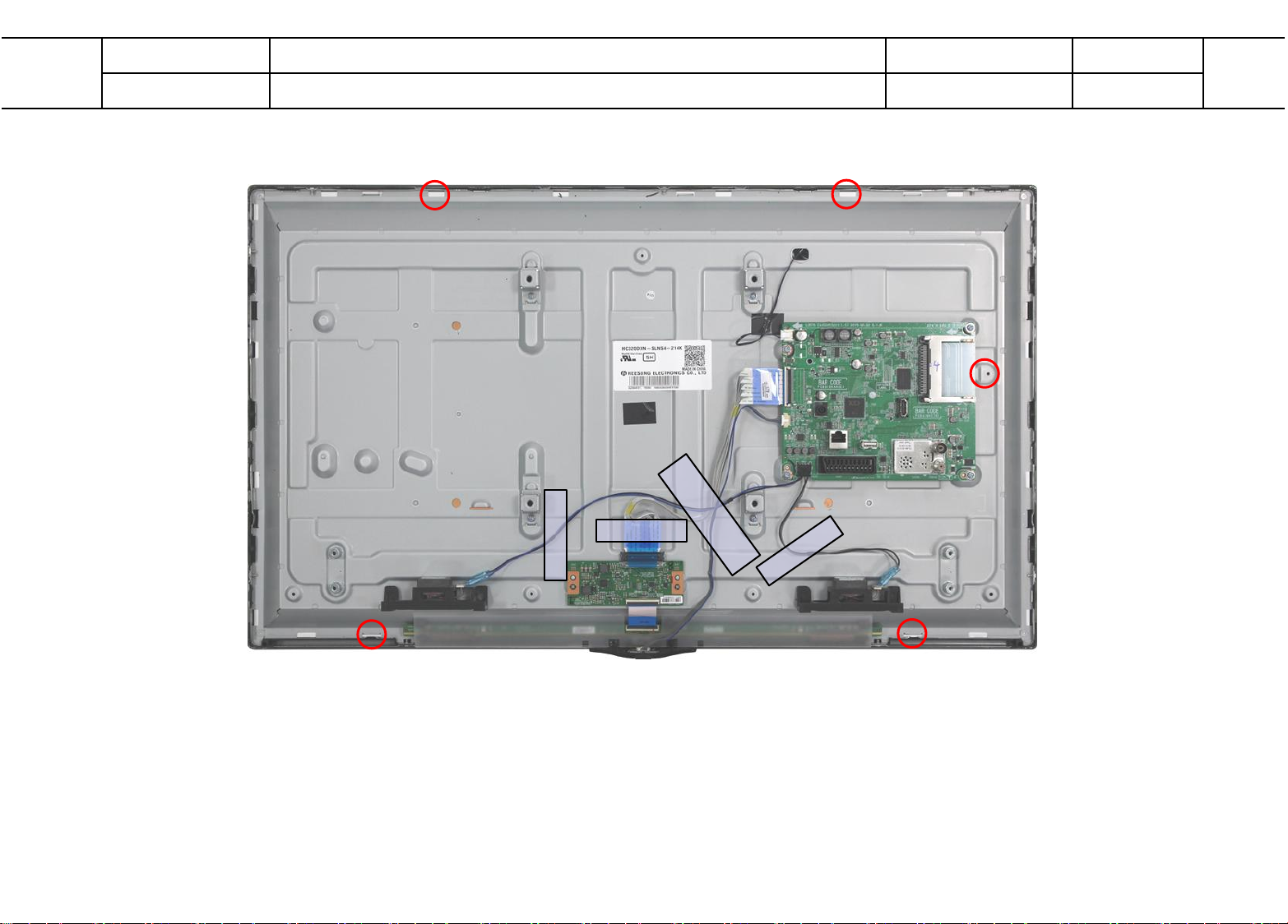
Standard Repair Process Detail Technical Manual
Power On -> disjoint back case -> check lighting
Error Symptom
A. Video Error, No Video/Normal Audio
Established date
2015.04.17
A1
Content
Check Back Light On with Naked eye
Revised date
Copyright © 2015 LG Electronics. Inc. All rights reserved.
Only for training and service purposes
LGE Internal Use Only
Page 52
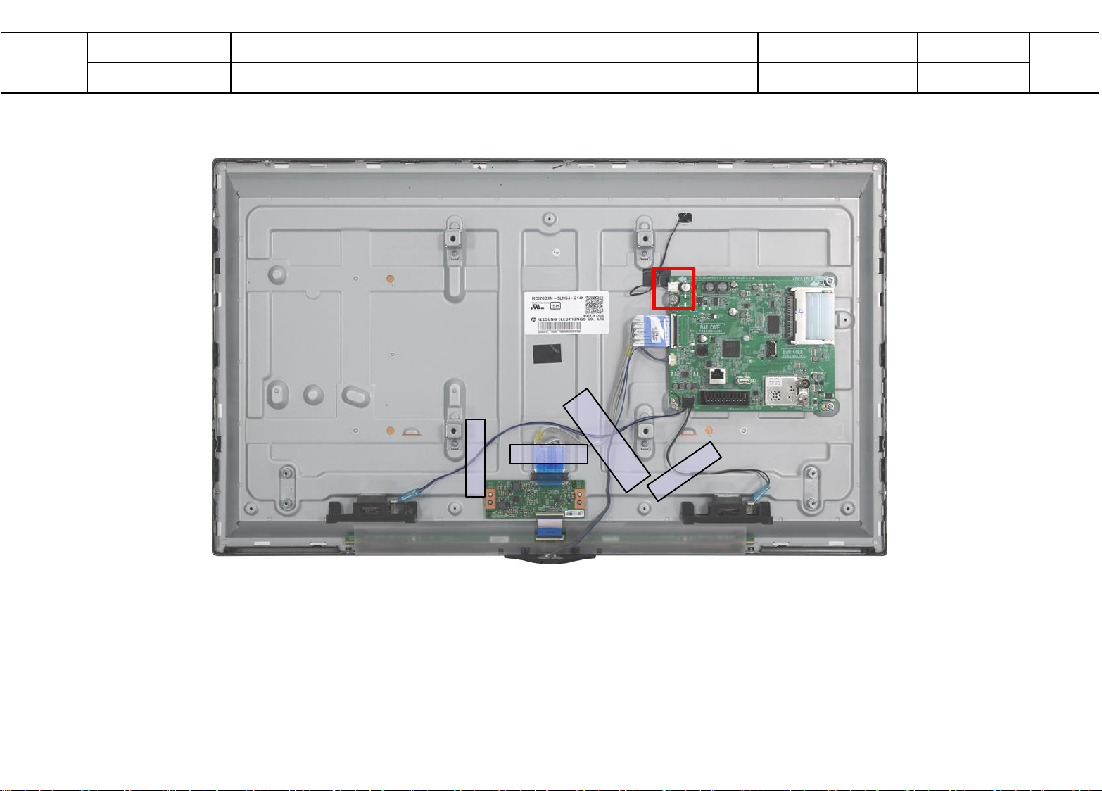
Standard Repair Process Detail Technical Manual
Measure DC Voltage applying to LED backlight from Main B/D
Error Symptom
A. Video Error, No Video/Normal Audio
Established date
2015.04.17
A2
Content
Main Board to LED back light Voltage
Revised date
Copyright © 2015 LG Electronics. Inc. All rights reserved.
Only for training and service purposes
LGE Internal Use Only
Page 53
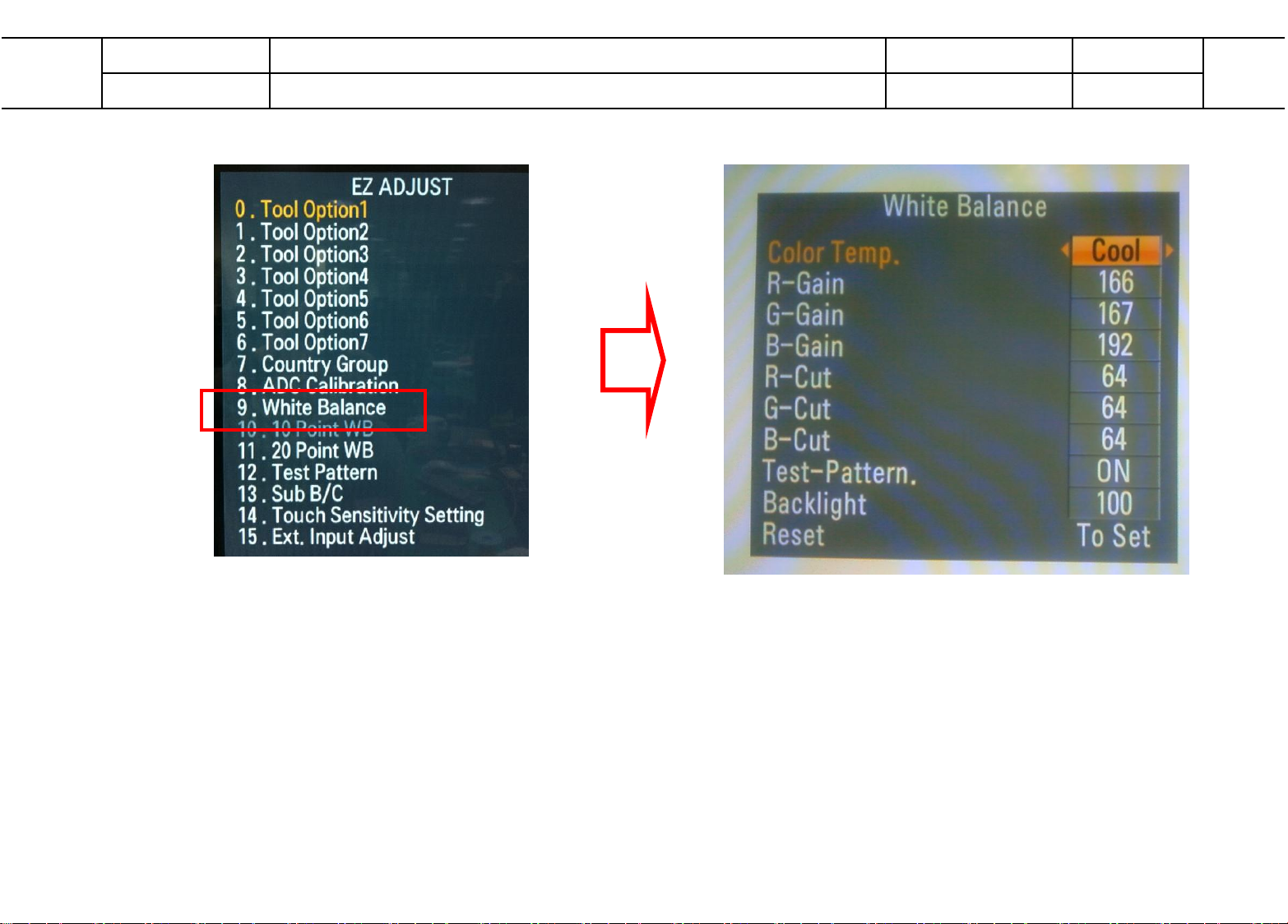
1. Press the ADJ button on the remote controller for adjustment
2. Enter into White Balance of item 9
3. After recording the R, G, B (GAIN, Cut) value of Color Temp (Cool/Medium/Warm),
re-enter the value after replacing the MAIN BOARD
Standard Repair Process Detail Technical Manual
Error Symptom
A. Video Error, No Video/Normal Audio
Established date
2015.04.17
A3
Content
Check White Balance value
Revised date
Copyright © 2015 LG Electronics. Inc. All rights reserved.
Only for training and service purposes
LGE Internal Use Only
Page 54
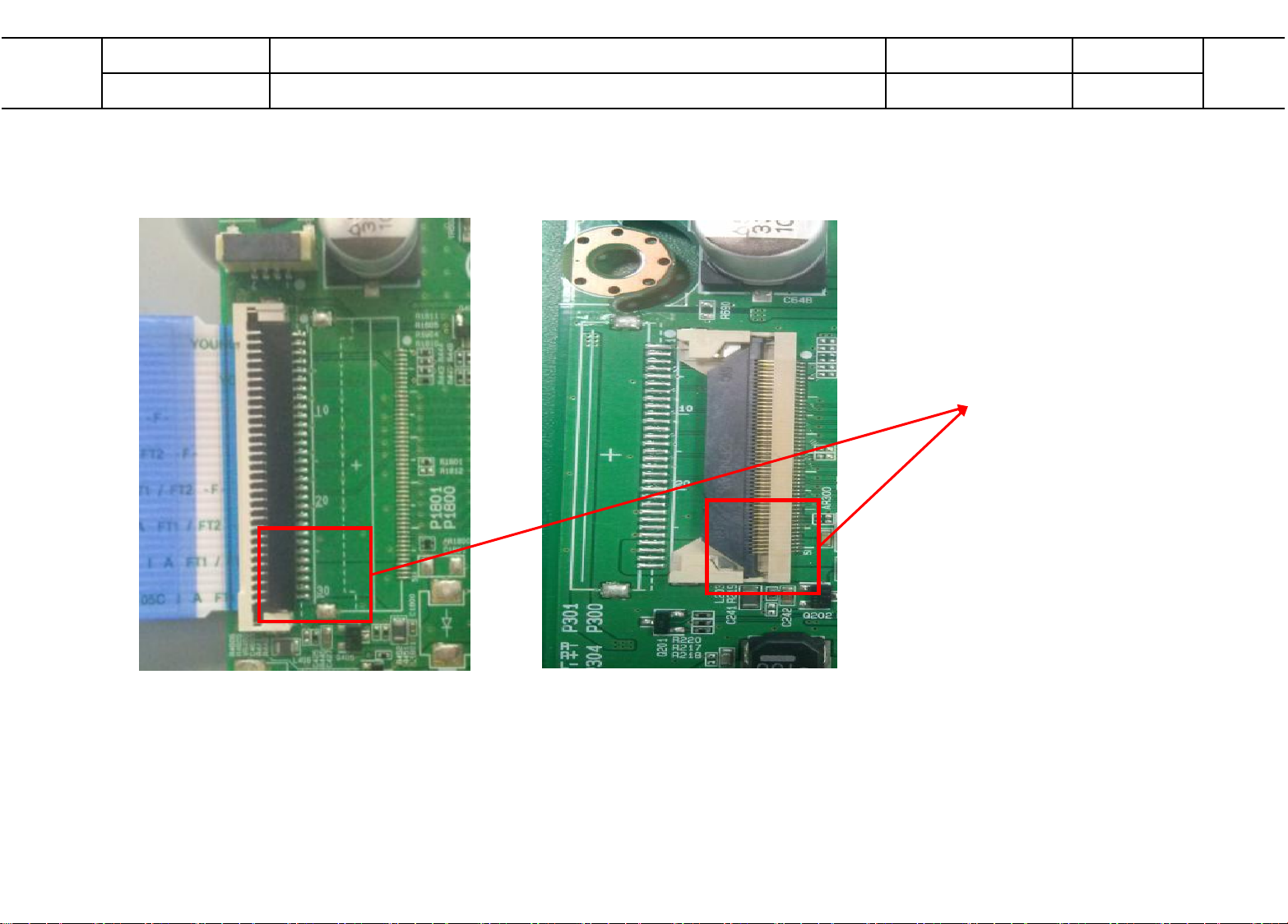
Standard Repair Process Detail Technical Manual
Check LVDS 12V
Error Symptom
A. Video Error, No Video/Normal Audio
Established date
2015.04.17
A4
Content
Power Voltage Measuring Method
Revised date
HD Model : 27 ~ 30 pin FHD Model : 48 ~ 51 pin
Copyright © 2015 LG Electronics. Inc. All rights reserved.
Only for training and service purposes
LGE Internal Use Only
Page 55
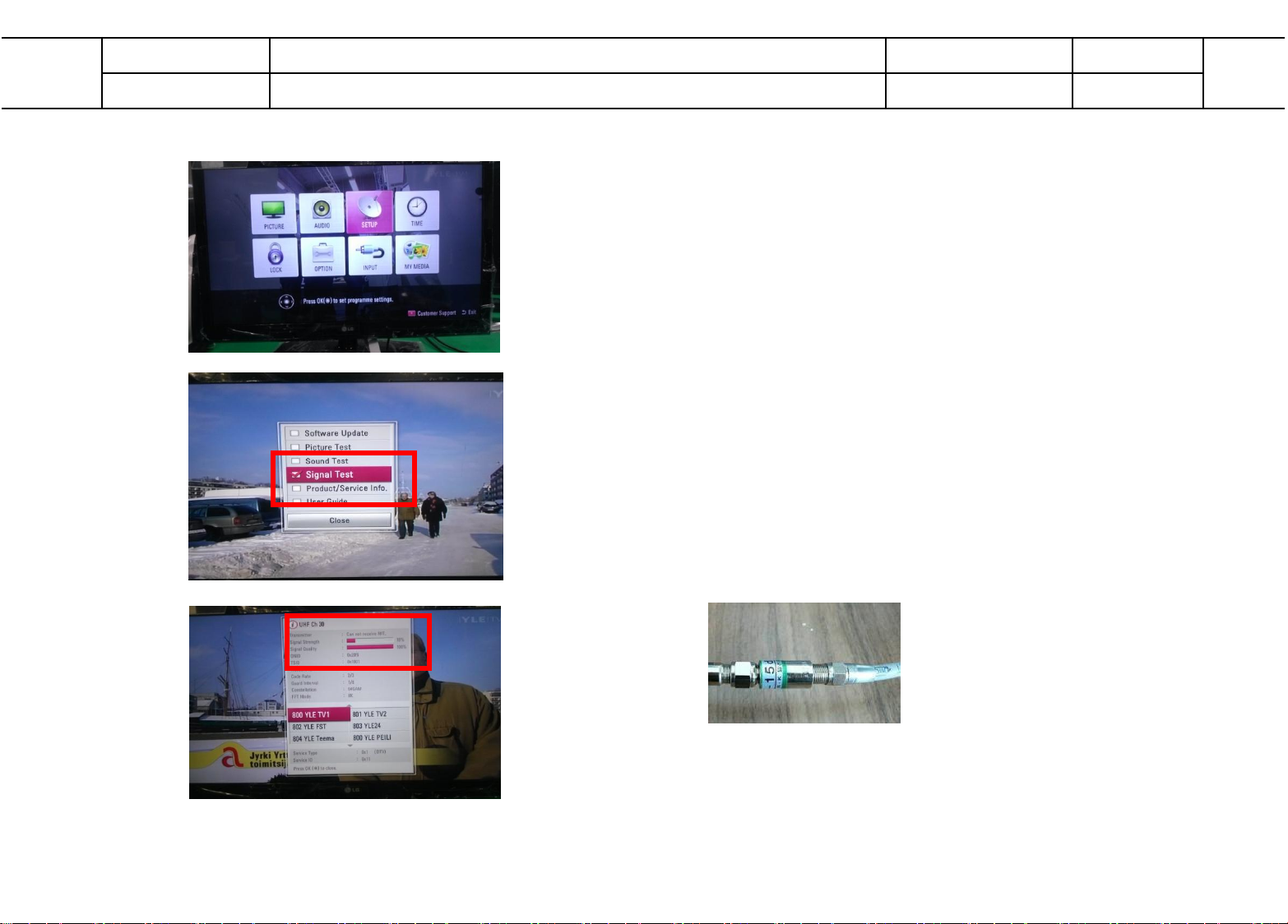
MENU Press red key Remote controller signal test
Select channel
When the signal is strong, use the
attenuator (-10dB, -15dB, -20dB etc.)
Standard Repair Process Detail Technical Manual
Error Symptom
A. Video Error, Video lag/stop
Established date
2015.04.17
A5
Content
Tuner Input Signal Strength Checking Method
Revised date
Copyright © 2015 LG Electronics. Inc. All rights reserved.
Only for training and service purposes
LGE Internal Use Only
Page 56
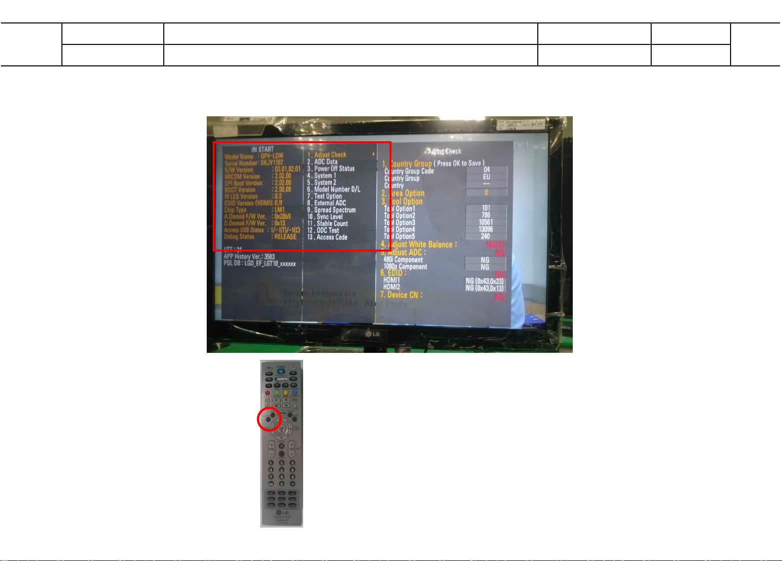
Standard Repair Process Detail Technical Manual
Checking SW version method for remote controller for adjustment
Press the IN-START with the remote
control for adjustment
Error Symptom
A. Video Error, No Video/Normal Audio
Established date
2015.04.17
A6
Content
TV Version Checking Method
Revised date
Copyright © 2015 LG Electronics. Inc. All rights reserved.
Only for training and service purposes
LGE Internal Use Only
Page 57
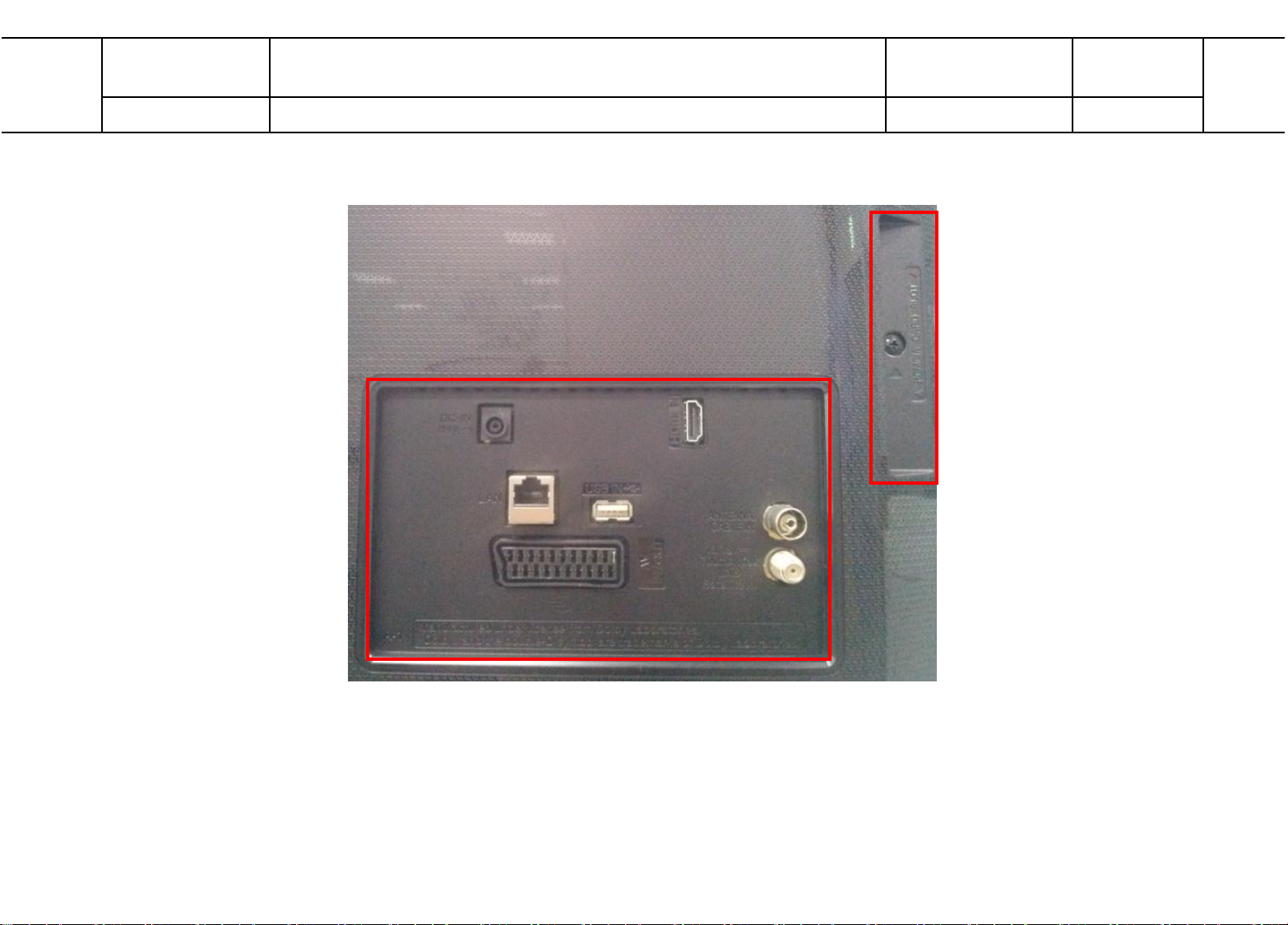
Standard Repair Process Detail Technical Manual
Error Symptom
A. Video Error, Vertical/Horizontal bar, Residual Image,
Light spot
Established date
2015.04.17
A7
Content
Connection diagram
Revised date
As the part connecting to the external input, check the
screen condition by signal
* Jack spec. : depending on Model
Copyright © 2015 LG Electronics. Inc. All rights reserved.
Only for training and service purposes
LGE Internal Use Only
Page 58
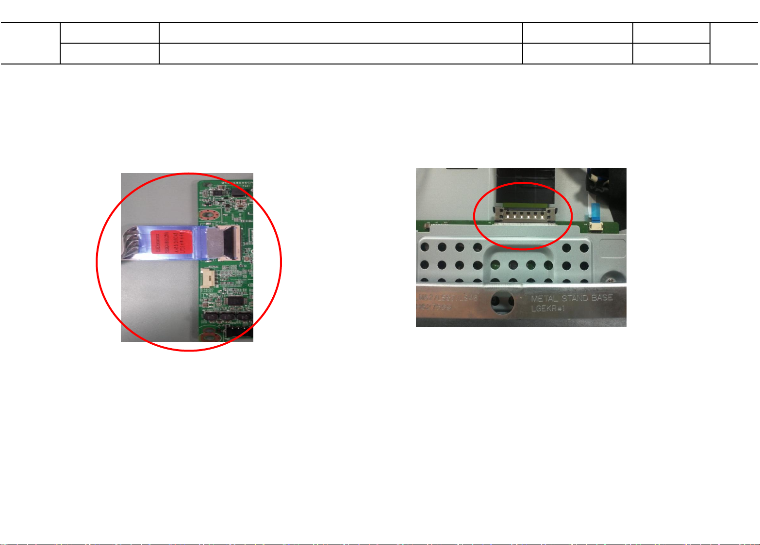
1. Check and replace LVDS Cable
2. Check LVDS connection condition
Standard Repair Process Detail Technical Manual
Error Symptom
A. Video Error, Color Error
Established date
2015.04.17
A8/
A9
Content
Check and replace Link Cable(LVDS) and contact condition
Revised date
Copyright © 2015 LG Electronics. Inc. All rights reserved.
Only for training and service purposes
LGE Internal Use Only
Page 59
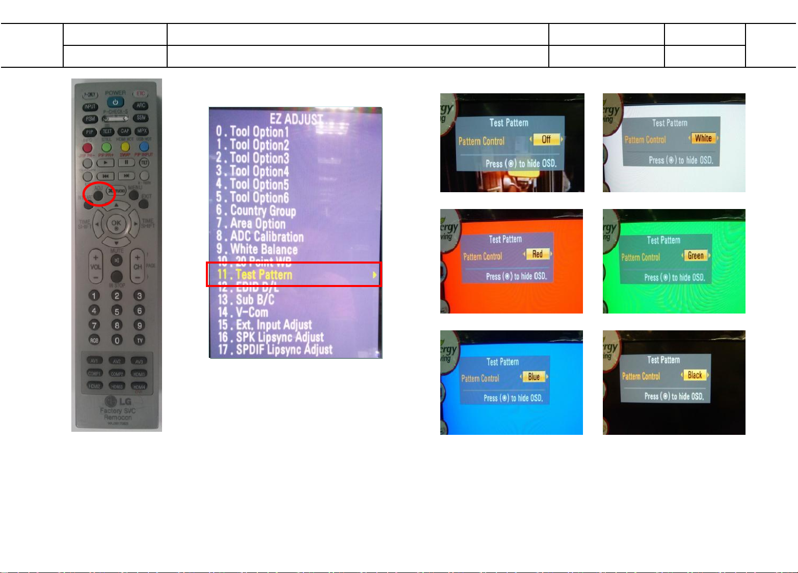
Standard Repair Process Detail Technical Manual
You can view 6 types of patterns using the ADJ Key
Checking item : 1. Defective pixel 2. Residual image 3. MODULE error (ADD-BAR,SCAN BAR..)
4.Video error (Classification of MODULE or Main-B/D)
Error Symptom
A. Video Error, Color Error
Established date
2015.04.17
A10
Content
Adjustment Test Pattern - ADJ Key
Revised date
Copyright © 2015 LG Electronics. Inc. All rights reserved.
Only for training and service purposes
LGE Internal Use Only
Page 60
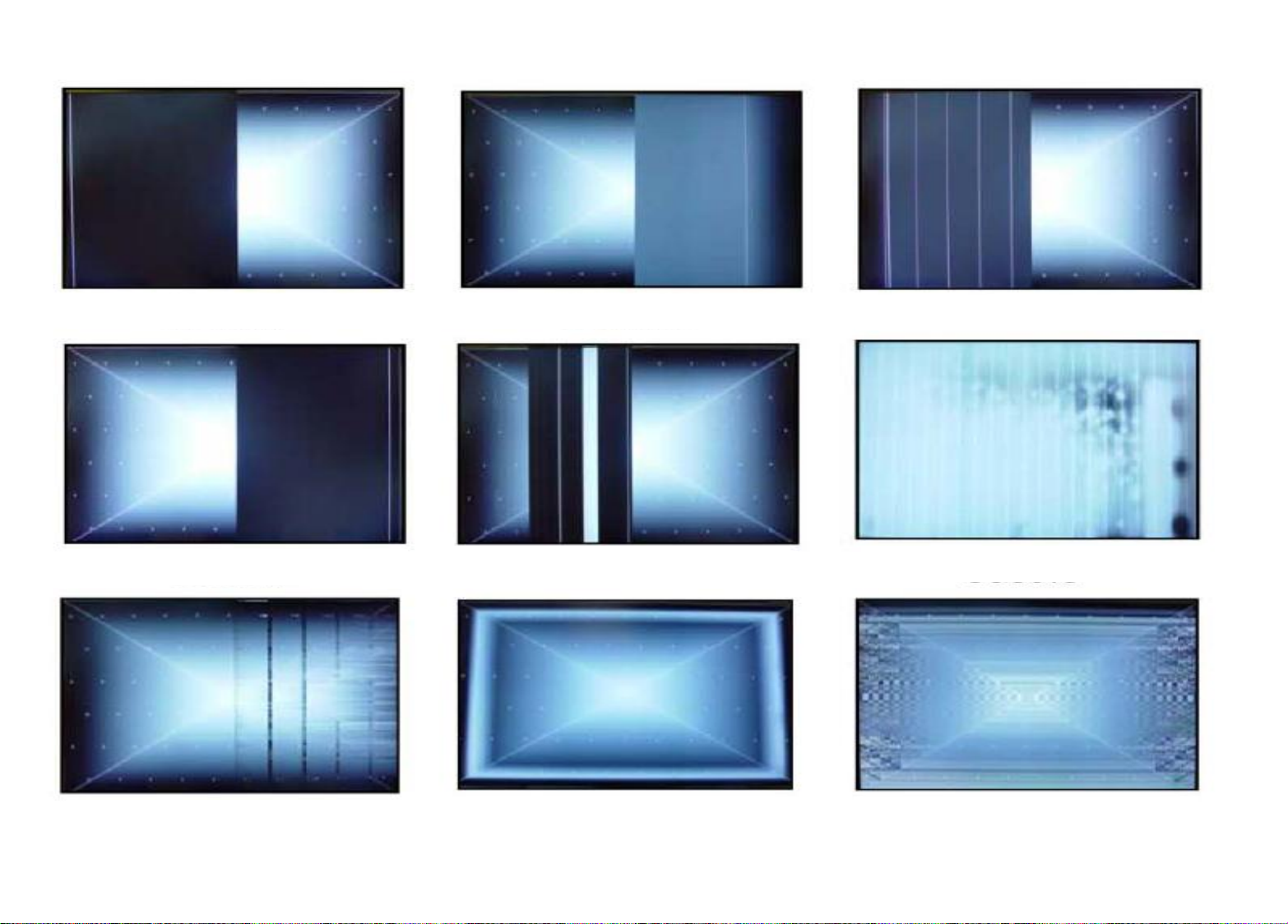
Solder defect, CNT Broken
T-Con Defect, CNT Broken
T-Con Defect, CNT Broken
T-Con Defect, CNT Broken
Solder defect, CNT Broken
Solder defect, CNT Broken
Solder defect, CNT Broken
Solder defect, CNT Broken
Abnormal Power Section
Solder defect, Short/Crack
Abnormal Power Section Solder defect, Short/Crack
Appendix : Exchange T-Con Board (1)
Copyright © 2015 LG Electronics. Inc. All rights reserved.
Only for training and service purposes
LGE Internal Use Only
Page 61
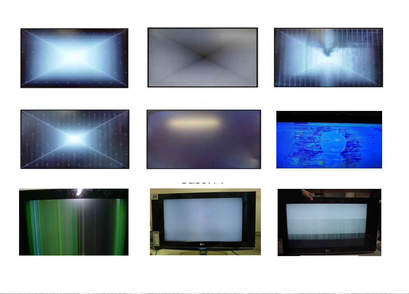
Abnormal Power Section
Solder defect, Short/Crack
Abnormal Power Section
Solder defect, Short/Crack
Fuse Open, Abnormal power section
Noise
GRADATION
GRADATION
Abnormal Display
Appendix : Exchange T-Con Board (2)
Copyright © 2015 LG Electronics. Inc. All rights reserved.
Only for training and service purposes
LGE Internal Use Only
Page 62
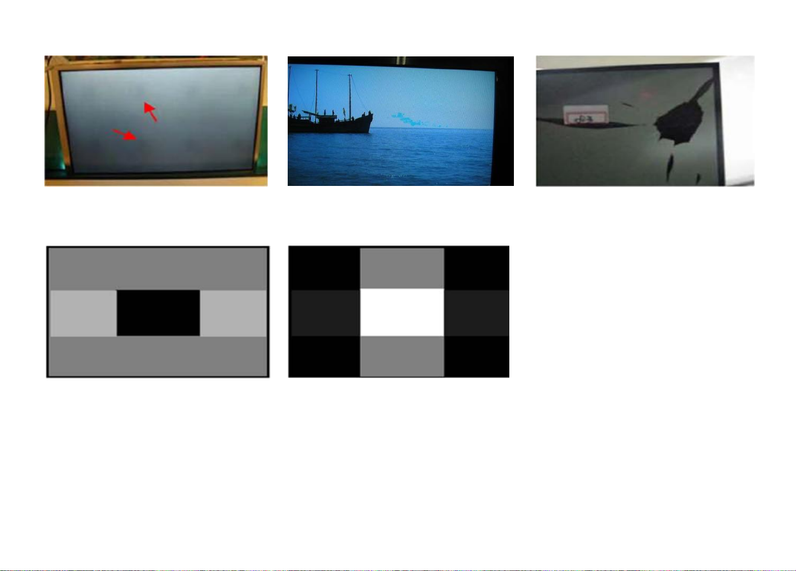
Appendix : Exchange the Module (1)
Crosstalk Crosstalk
Press damage Press damage
Un-repairable Cases
In this case please exchange the module.
Press damage
Copyright © 2015 LG Electronics. Inc. All rights reserved.
Only for training and service purposes
LGE Internal Use Only
Page 63
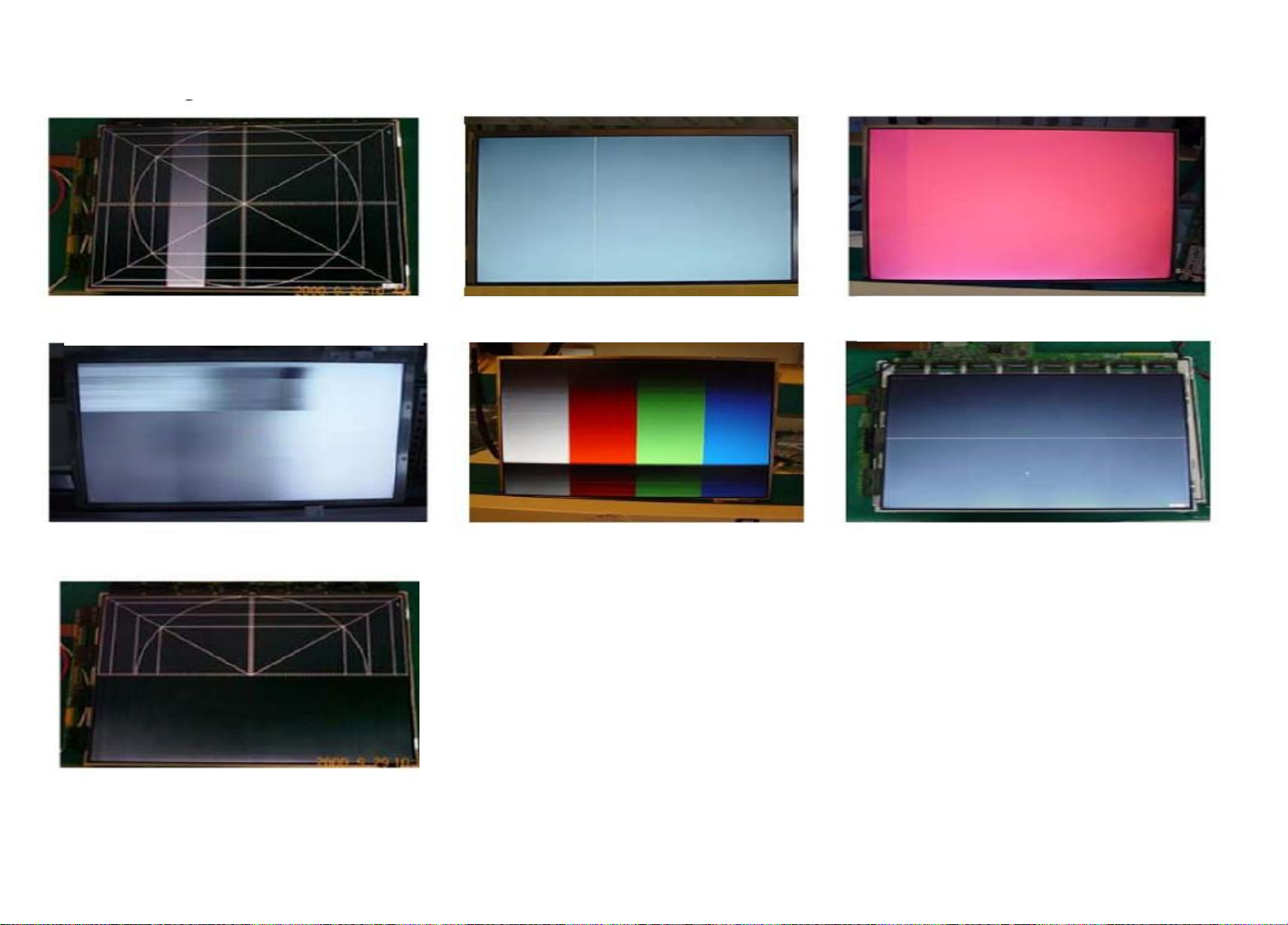
Vertical Block
Source TAB IC Defect
Horizontal Block
Gate TAB IC Defect
Gate TAB IC Defect
Gate TAB IC Defect
Vertical Line
Source TAB IC Defect
Vertical Block
Source TAB IC Defect
Horizontal Block
Gate TAB IC Defect
Horizontal line
Gate TAB IC Defect
Gate TAB IC Defect
Horizontal Block
Gate TAB IC Defect
Appendix : Exchange the Module (2)
Un-repairable Cases
In this case please exchange the module.
Copyright © 2015 LG Electronics. Inc. All rights reserved.
Only for training and service purposes
LGE Internal Use Only
Page 64
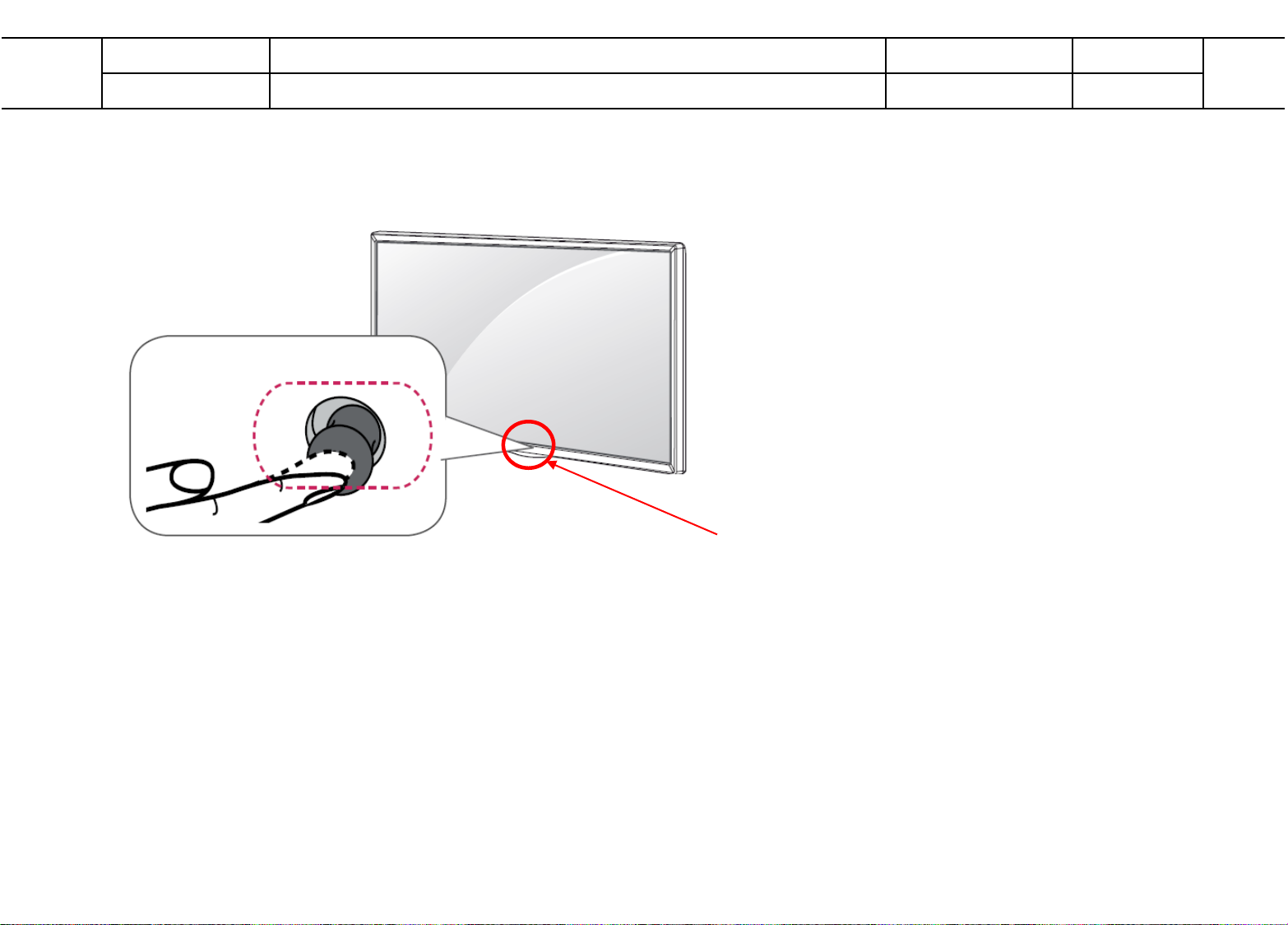
Standard Repair Process Detail Technical Manual
ST-BY condition: Red
Front LED control :
Menu Option Standby Light On/Off
Error Symptom
B. Power Error, No Power
Established date
2015.04.17
A11
Content
Check front Display LED
Revised date
Copyright © 2015 LG Electronics. Inc. All rights reserved.
Only for training and service purposes
LGE Internal Use Only
Page 65
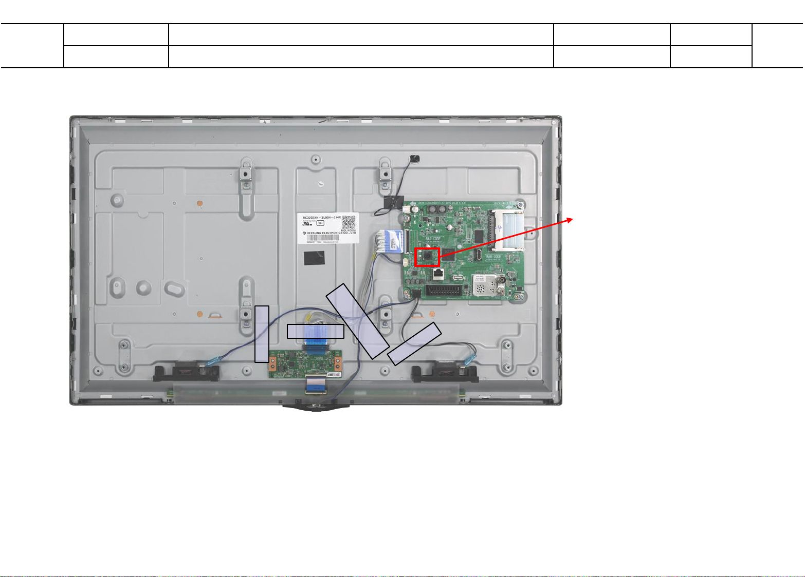
Standard Repair Process Detail Technical Manual
Check Voltage 19V of Adaptor Power
Error Symptom
B. Power Error, No Power
Established date
2015.04.17
A12/
A13
Content
Checking Method When Power is ON
Revised date
Copyright © 2015 LG Electronics. Inc. All rights reserved.
Only for training and service purposes
LGE Internal Use Only
Page 66
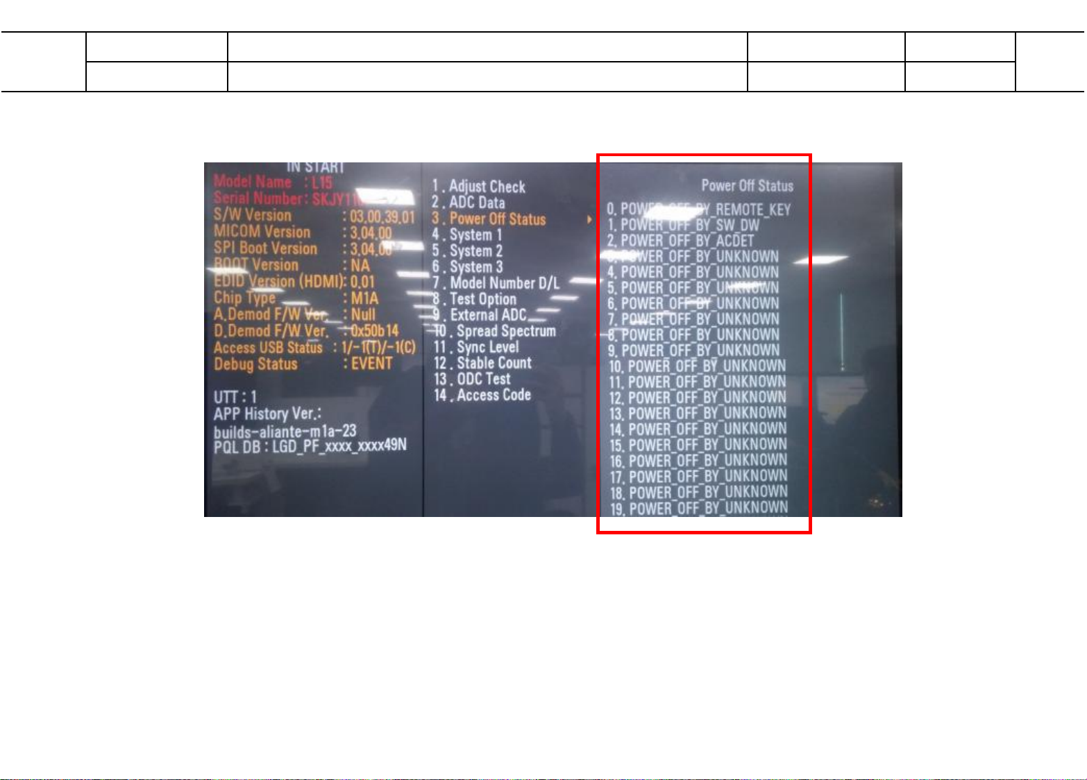
1. Press the IN-START button of the remote controller for adjustment
2. Check the entry into adjustment item 3
Standard Repair Process Detail Technical Manual
Error Symptom
B. Power Error, Off when on, off whiling viewing
Established date
2015.04.17
A14
Content
Power off Mode checking method
Revised date
Copyright © 2015 LG Electronics. Inc. All rights reserved.
Only for training and service purposes
LGE Internal Use Only
Page 67
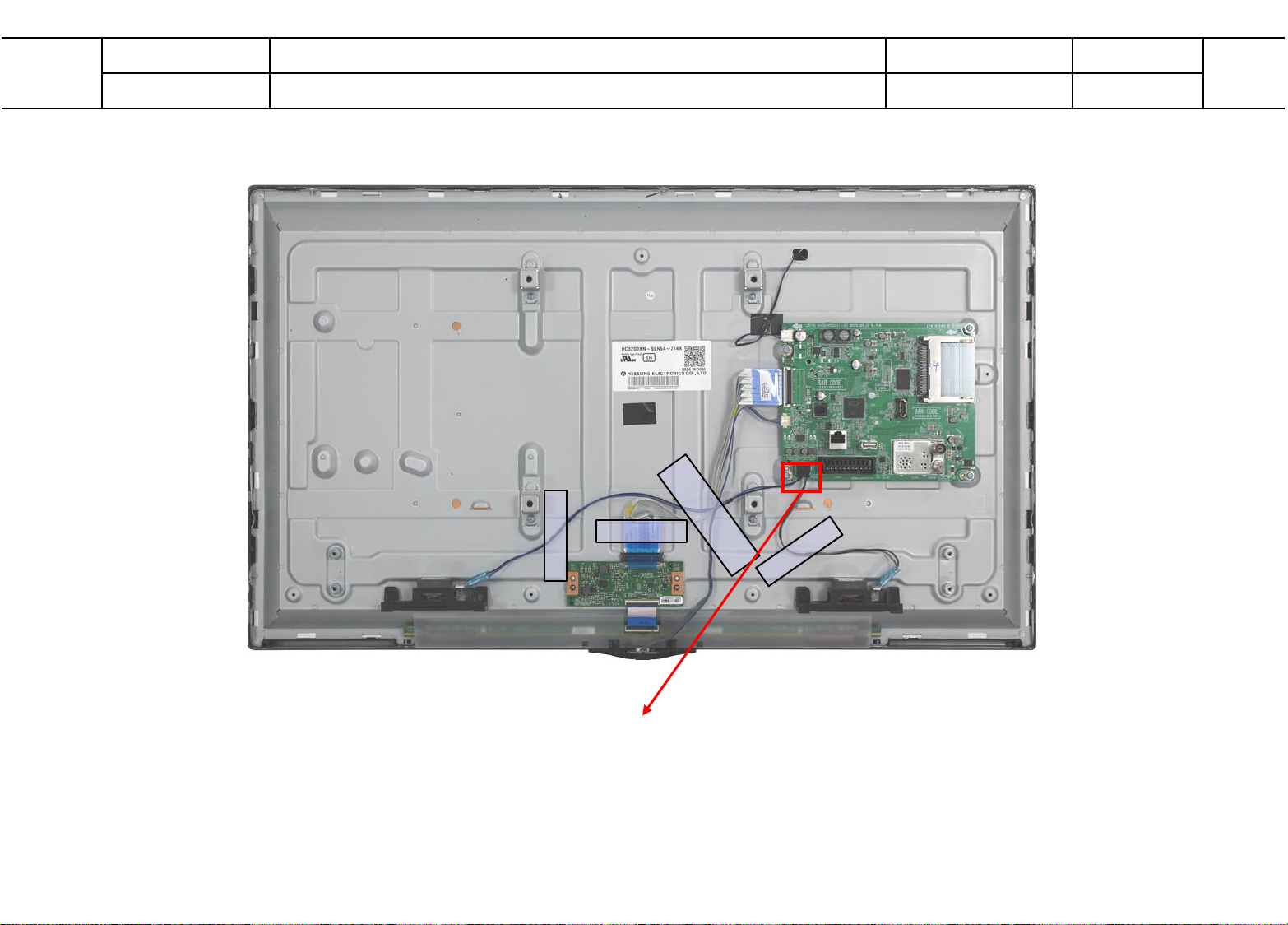
Check Connection from Main B/D to Speaker
Standard Repair Process Detail Technical Manual
Error Symptom
C. Audio Error, No Audio/Normal Video
Established date
2015.04.17
A15
Content
Checking method in menu when there is no audio
Revised date
Copyright © 2015 LG Electronics. Inc. All rights reserved.
Only for training and service purposes
LGE Internal Use Only
Page 68
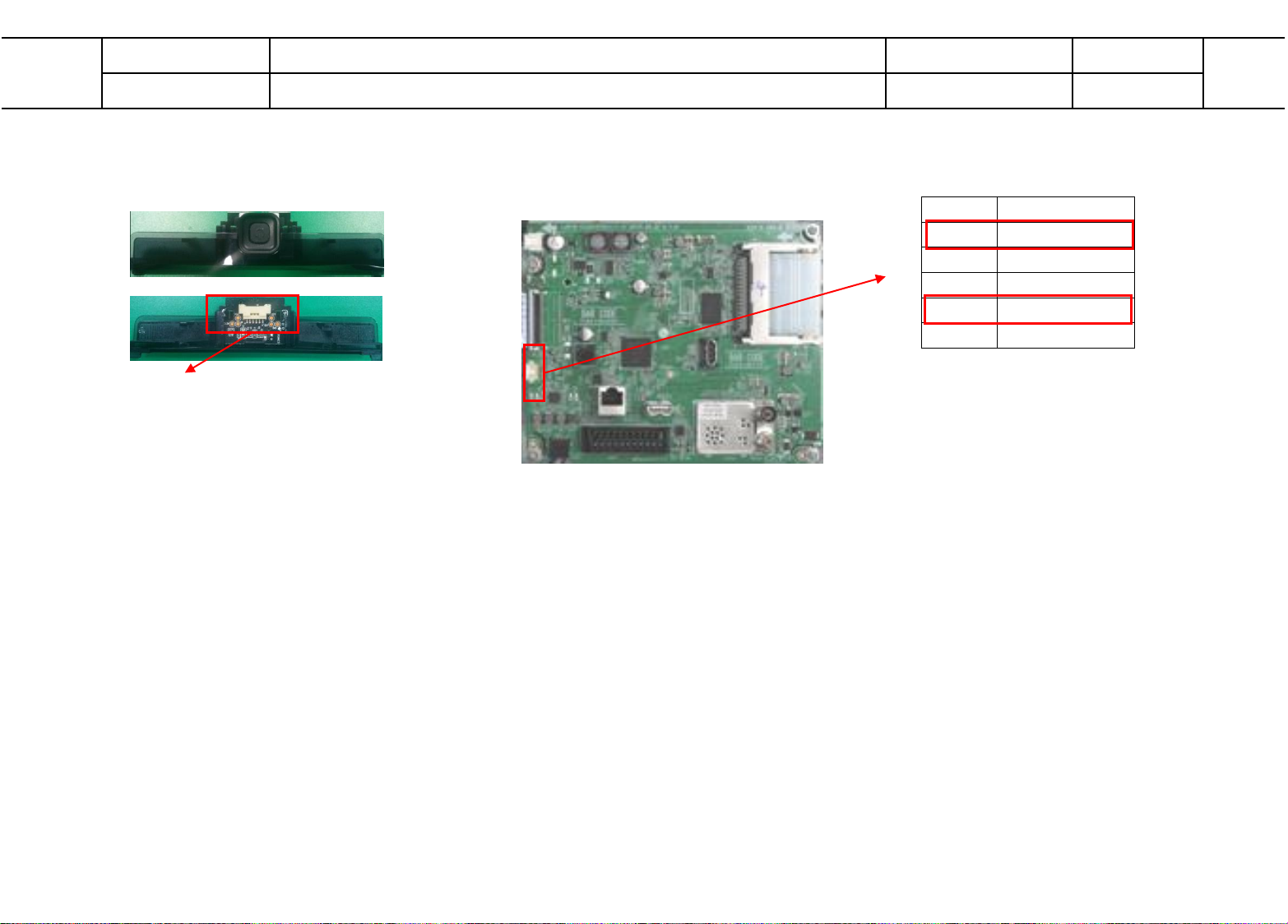
1
KEY2
2
3.5V_ST
3
GND
4
LED_R/BUZZ
5
IR
6
GND
1, 2. Check IR cable condition between IR & Main board
3. Check the ST-BY 3.5V on the terminal 4
4. When checking the Pre-Amp when the power is in ON condition, it is normal when the Analog
Tester needle moves slowly, and defective when it does not move at all.
Standard Repair Process Detail Technical Manual
①
②
③
④
P4600
< Sub Ass’y>
< Main Ass’y>
Error Symptom
D. Function Error, No Response in remote controller, Key error
Established date
2015.04.17
A16
Content
Remote controller operation checking method
Revised date
Copyright © 2015 LG Electronics. Inc. All rights reserved.
Only for training and service purposes
LGE Internal Use Only
 Loading...