

Page 1
LG TRAINING MANUAL
LG TRAINING MANUAL
Fall 2008 PDP Training
42PG20
50PG20
Page 2
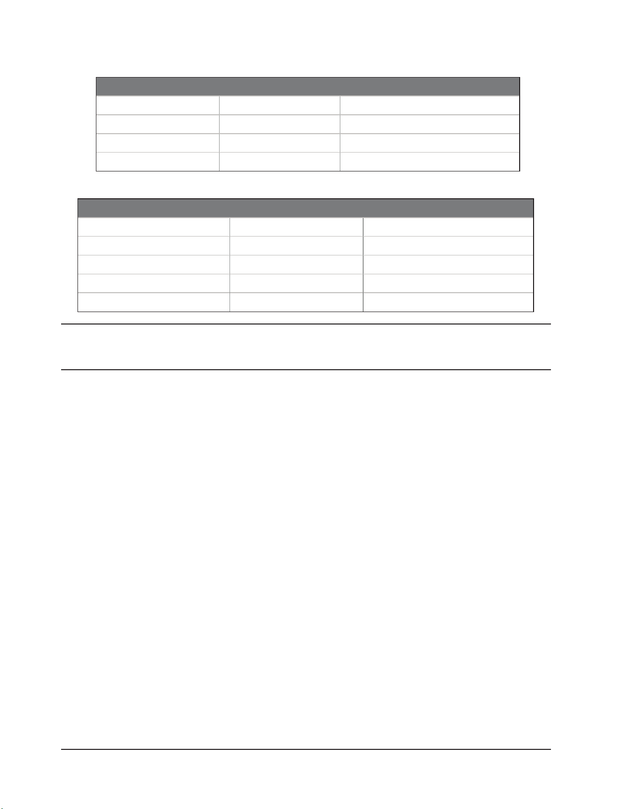
Ph o n e Co n t a C t s :
Contact Number Hours of Operation
Customer Service (800) 243-0000 24 hours a day / 7 days a week
Technical Support (800) 847-7597 7am-7pm Mon-Fri / Sat 8-2 CT
Parts Sales (888) 393-6484 7am-7pm Mon-Sat CT
Training Center (256) 774-4051 8am-5pm Mon-Fri CT
We b Co n t a C t s :
Web Site Address Description
LG USA www.lgusa.com Product information
Customer Service us.lgservice.com User manuals, FAQs
GCSC aic.lgservice.com Service manuals, parts, bulletins
Customer Service Academy www.lgcsacademy.com Web training, discussion forum
Live Training lge.webex.com Live training
Published July 2008 by LG Electronics USA Training Center
Copyright © 2008 LG Electronics of Alabama, Inc.
IMPORTANT SAFETY NOTICE
This manual was prepared for use only by properly trained audio-visual service technicians. When servicing this product, under no circumstances
should the original design be modified or altered without permission from LG Electronics. Unauthorized modifications will not only void the
warranty, but may lead to property damage or user injury. All components should be replaced only with types identical to those in the original
circuit and their physical location, wiring, and lead dress must conform to original layout upon completion of repairs. If any fuse (or Fusible
Resistor) in this TV receiver is blown, replace it only with the factory specified fuse type and rating. When replacing a high wattage resistor
(Oxide Metal Film Resistor, over 1W), keep the resistor 10mm away from PCB. Always keep wires away from high voltage or high temperature
parts. Do not attempt to modify this product in any way.
Special components are also used to prevent shock and fire hazard and are required to maintain safe performance. No deviations are allowed
without prior approval by LG Electronics. Service work should be performed only after you are thoroughly familiar with these safety checks and
servicing guidelines. Circuit diagrams may occasionally differ from the actual circuit used. This way, implementation of the latest safety and
performance improvement changes into the set is not delayed until the new service literature is printed.
ElECTROSTATICAllY SENSITIvE DEvICES
Some semiconductor (solid-state) devices can be damaged easily by static electricity. Such components commonly are called Electrostatically
Sensitive (ES) Devices. Examples of typical ES devices are integrated circuits and some field-effect transistors and semiconductor “chip” components.
The following techniques should be used to help reduce the incidence of component damage caused by static electricity.
Immediately before handling any semiconductor component or semiconductor-equipped assembly, drain off any electrostatic charge on the
body by touching a known earth ground. Alternatively, obtain and wear a commercially available discharging wrist strap device, which should
be removed for potential shock reasons prior to applying power to the unit under test. After removing an electrical assembly equipped with ES
devices, place the assembly on a conductive surface such as an ESD mat, to prevent electrostatic charge buildup or exposure of the assembly.
Use only a grounded-tip soldering iron to solder or unsolder ES devices. Use only an anti-static solder removal device. Some solder removal
devices not classified as “anti-static” can generate electrical charges sufficient to damage ES devices. Do not use refrigerant-propelled chemicals
which can generate electrical charge sufficient to damage ES devices. Do not remove a replacement ES device from its protective package until
immediately before you are ready to install it.
REGUlATORY INFORMATION
This equipment has been tested and found to comply with the limits for a Class B digital device, pursuant to Part 15 of the FCC Rules. These limits
are designed to provide reasonable protection against harmful interference when the equipment is operated in a residential installation. This
equipment generates, uses and can radiate radio frequency energy and, if not installed and used in accordance with the instruction manual, may
cause harmful interference to radio communications. However, there is no guarantee that interference will not occur in a particular installation.
If this equipment does cause harmful interference to radio or television reception, which can be determined by turning the equipment off and
on, the user is encouraged to try to correct the interference by one or more of the following measures: Reorient or relocate the receiving antenna;
Increase the separation between the equipment and receiver; Connect the equipment into an outlet on a circuit different from that to which the
receiver is connected; Consult the dealer or an experienced radio/TV technician for help.
The responsible party for this device’s compliance is: LG Electronics of Alabama, Inc. 201 James Record Road. Huntsville, AL 35813, USA. Digital
TV Hotline: 1-800-243-0000
Page 3

Page 4

Spring 2008 PDP Training
Page 5

Table of ConTenTs
OVERVIEW .................................................. 5
Introduction ....................................................5
Basic Troubleshooting Steps ...........................5
Caution............................................................5
Model Number Structure ...............................6
Serial Number Structure .................................6
Remote Control ..............................................7
New Features .................................................7
Computer Connection ....................................8
Service Menu ...................................................8
Power Consumption .......................................8
Service Remote ...............................................9
Check Firmware Version ............................. 10
Update Firmware ......................................... 10
42PG20 Dimensions .................................... 11
50PG20 Dimensions .................................... 11
DISASSEMBLY ........................................... 12
Introduction ................................................. 12
Back Cover Removal .................................... 12
Switch Mode Power Supply Removal .......... 13
Y-Sus board Removal .................................... 13
Y-Drive board Removal ............................... 13
Z-Sus board Removal ................................... 13
Main board Removal .................................... 13
Control Button Board Removal ................... 13
X-Drive boards Removal .............................. 13
TCP Connector Removal ............................. 15
P232 & P331 Connector Removal ............... 15
Control Button board removal .................... 16
42PG20 Exploded View ............................... 17
Block Diagram .............................................. 18
Signal and Voltage Block Diagram ................ 19
CIRCUIT DESCRIPTIONS ......................... 20
Introduction ................................................. 20
Adjustment Order **Important**................ 20
Power Supply (SMPS) ................................... 21
Y-Sus Board .................................................. 29
Y-Drive Board .............................................. 37
Z-Sus Board ................................................. 42
Control Board .............................................. 44
X-Drive Boards ............................................ 51
Left and Right X-Drive Removal .................. 55
Main (Digital) Board ..................................... 56
Power Switch and Keypad ........................... 61
DISASSEMBLY ........................................... 63
Introduction ................................................. 63
Back Cover Removal .................................... 63
Power Supply Board Removal ...................... 63
Y-Sus Board Removal ................................... 64
Top Y-Drive Board Removal ......................... 64
Bottom Y-Drive Board ................................. 64
Z-Sus Board Removal ................................... 65
Main Board Removal .................................... 65
Control Board Removal ............................... 65
X-Board Removal ......................................... 65
TCP connector removal ............................... 67
P232 & P331 connector removal ................. 67
50PG20 Exploded View ............................... 68
Block Diagram .............................................. 69
Signal and Voltage Block Diagram ................ 70
CIRCUIT DESCRIPTIONS ........................ 71
Introduction ................................................. 71
Adjustment Order **Important**................ 72
Power Supply ............................................... 72
Y-Sustain ....................................................... 82
Y-drive .......................................................... 88
Z-Sus Board ................................................. 93
Control Board .............................................. 97
X-Drive Boards .......................................... 102
Left and Right X-Drive Removal ................ 107
Main (Digital) Board ................................... 108
SCHEMATICS .......................................... 111
42PG20 :: Interconnect .............................. 111
42PG20 :: Waveforms ................................ 112
42PG20 :: Main Board :: Video & BCM ...... 113
42PG20 :: Main Board :: Control ............... 114
42PG20 :: Main Board :: DDR Memory ..... 115
42PG20 :: Main Board :: Tuner ................... 116
42PG20 :: Main Board :: Audio Processor . 117
42PG20 :: Main Board :: Power Regulator . 118
42PG20 :: Main Board :: Inputs .................. 119
42PG20 :: Main Board :: HDMI & USB ...... 120
42PG20 :: Power Supply :: PFC & MCU .... 121
42PG20 :: Power Supply :: Multi & Stby..... 122
42PG20 :: Power Supply :: VA & VA .......... 123
42PG20 :: Main Board :: PCB Layout ......... 124
42PG20 :: Main Board :: Bottom PCB ....... 125
42PG20 :: Sub Boards :: PCB Layout ......... 126
50PG20 :: Main Board :: Interconnect ....... 127
50PG20 :: Main Board :: Control ............... 128
50PG20 :: Main Board :: Video & BCM ...... 129
50PG20 :: Main Board :: Control ............... 130
50PG20 :: Main Board :: DDR Memory ..... 131
50PG20 :: Main Board :: Tuner ................... 132
50PG20 :: Main Board :: Audio Processor . 133
50PG20 :: Main Board :: Power Regulator . 134
50PG20 :: Main Board :: Interface .............. 135
50PG20 :: Main Board :: HDMI & USB ...... 136
50PG20 :: Main Board :: PCB Layout ......... 137
50PG20 :: Main Board :: Bottom PCB ....... 138
50PG20 :: Sub Boards :: PCB Layout ......... 139
PDP Training - Fall 2008 3
Page 6

- 4 -
Page 7

OVERVIEW
OVERVIEW 2008 PDP
INTRODUCTION
This manual covers two models from the 2008 Plasma Display Panel (PDP) product line.
Each model is an HDTV with integrated HD tuner. All 2008 PDP models include USB Media
Host and SimpLink. USB Media Host consists of a USB port on the back of the TV that
supports USB flash memory drives loaded with media or firmware for the TV. SimpLink
allows for control of other LG SimpLink products via the HDMI connection.
All PDP TV models are covered by a one year parts and labor warranty. Refer to the last
page of the owner’s manual for more warranty information. When making a warranty repair
involving a service bulletin, be sure to refer to the service bulletin number in the warratny
claim.
BASIC TROUBLESHOOTING STEPS
Define - Look at the symptom carefully and determine what circuits could be causing the
failure. Use your senses Sight, Smell, Touch and Hearing. Look for burned parts and
check for possible overheated components. Capacitors will sometimes leak dielectric
material and give off a distinct odor. The frequency of power supplies will change with
the load, or listen for a relay closing, etc. Observation of the front Power LED may
give some clues.
Localize - Carefully check the symptom and determining the circuits to be checked. After
giving a thorough examination using your senses, check the DC Supply Voltages to
those circuits under test. Always confirm the supplies are not only the proper level,
but are noise free. If the supplies are missing check the resistance for possible short
circuits.
Isolate - To further isolate the failure, check for the proper waveforms with an Oscilloscope
to make a final determination of the failure. Look for correct Amplitude Phasing and
Timing of the signals. Also check for the proper Duty Cycle of the signals. Sometimes
“glitches” or “road bumps” will be an indication of an imminent failure.
Correct - The final step is to correct the problem. Be careful of static sensitive components
and make sure to check the DC Supplies for proper levels. Make all necessary
adjustments. Lastly, always perform a Safety AC Leakage Test before returning the
product back to the Customer.
CAUTION
1) A (approximately) 10 minute pre-run time is required before any adjustments are
performed.
PDP Training - Fall 2008 5
Page 8
OVERVIEW
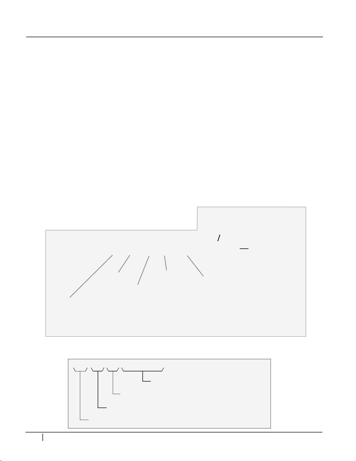
403 MX XQ
0 5 1 0 6
Sequential Number (5-7 Numbers)
Production Info (2 Letters)
Production Site (2 Letters)
Production Year and Month (3 Numbers). Ex, March 2004.
5 0 P G 2 0 - U A
Screen Size
Year
G = 2008
Series/Feature Level
20/25 = 720p HDTV
30 = Full HD
60 = Full HD & THX
Display Type
P = Plasma
L = LCD
D = DLP RPTV
J = Projector
Brand
Z= Zenith
Blank = LG
Region
U = North America
B = Europe & NA
Chassis Version
2) Refer to the Voltage Sticker inside the panel when making adjustments on the Power
Supply, Y-Sus and Z-Sus boards and adjust to the specified voltage level (±1/2 V).
3) The PDP module uses high voltage, be cautious of electric shock from the PDP
module. Before circuit board removal, check that the Power Supply and drive circuits
are completely discharged because of residual current stored.
4) C-MOS circuits are used extensively for processing the Drive Signals and should be
protected from static electricity.
5) The Plasma television and/or PDP Module must be carried/transported vertical, not
horizontal. (If laying down on its face, foam padding is a must).
6) Exercise care when making voltage and waveform checks to prevent costly short circuits
from damaging the unit.
7) Be cautious of loose screws and other metal objects to prevent a possible short in the
circuitry.
8) New panels and frames are much thinner than previous models. Be Careful with flexing
these panels. Be careful with lifting panels from a horizontal position. Damage to the
Frame mounts or panel can occur.
MODEL NUMBER STRUCTURE
SERIAL NUMBER STRUCTURE
6 PDP Training - Fall 2008
Page 9
INPUT
FAV
MUTE
TV
STB
POWER
Q. MENU MENU
AV MODERETURN
ENTER
VOL
CH
1 2 3
4 5 6
7 8
0
9
FLASHBK
P
A
G
E
DVD
VCR
REMOTE CONTROL
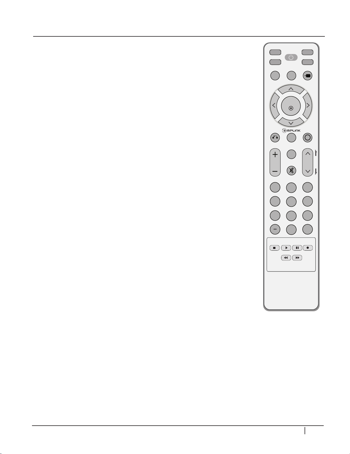
2008 models feature a newly designed, easier to use remote. The remote
has fewer buttons than previous designs which was accomplished by
moving many functions to an on-screen Quick Menu. The “Q. MENU”
button on the remote opens the Quick Menu and the user can choose
between options like aspect ratio, closed captions, sleep timer, etc.
The remotes are programmable for other devices. They also support
SimpLink devices. When using SimpLink, the device buttons on the
remote do not need to be pressed to switch modes before controlling
external equipment. So, the External devices are controlled by the TV
instead of the remote.
NEW FEATURES
Below are some of the new features on some 2008 PDP TVs.
FluidMotion (180Hz Effect) - Enjoy smoother, clearer motion with all
types of programming such as sports and action movies. The moving
picture resolution give the impression of performance of up to 3x
the panels actual refresh rate.
OVERVIEW
Full HD 1080p Resolution - Displays HDTV programs in full 1920 x
1080p resolution for a more detailed picture. Standard HD PDPs
are 1365 x 768p.
Expert Menu - Expert Menu features Imaging Science Foundation
Certified Calibration Controls (ISFccc) which allow precise in-home
picture calibrations.
Public Display Mode - This is an additional menu with advanced startup
options like startup volume, start channel, etc. This can be accessed
by holding the Menu key until it vanishes. Then key in 1, 1, 0, 5,
and press enter.
PDP Training - Fall 2008 7
Page 10
OVERVIEW
COMPUTER CONNECTION
A computer can be connected to the RGB (VGA)
or HDMI connection on the TV. The HDMI
connection will require a DVI to HDMI adapter
if the PC has a DVI connector.
Set the monitor output resolution and vertical
frequency on the PC before connecting it to
the TV. Refer to the owner’s manual for a full
list of suported resolutions, some examples are
listed below. The message “OUT OF RANGE”
will appear on the screen if the resoultion is not
supported.
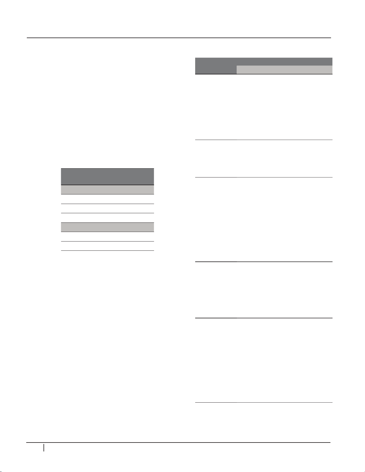
Resolution Vertical
30/40/50/60/70 series
1280x768 60Hz
1360x768 60Hz
1366x768 60Hz
50/60/70 series only
1600x1200 60Hz
1920x1080 60Hz
SERVICE MENU
The service menus can be used to make
adjustments, change color alignment, and get
software versions. There are two service menus.
The Adjust and Instart menu can be accessed
using the service remote (Service remotes are
available from LG parts). They can also be
accesed by holding down the menu button on
the TV and the remote until the user menu
disappears. The menus alternate between Adjust
and Instart every time the menu button is held
down. If the TV asks for a password, enter 0000
(four zeros).
POWER CONSUMPTION
Model
19LS4D-UA 42W 0.85 1W
20LS7D-NB 56W 0.85 1W
20LS7D-UK 56W 0.85 1W
22LC2D-UB 46W 0.85 1W
22LS4D-UA 46W 0.85 1W
23LS7D-NB 78W 0.85 1W
23LS7D-UK 78W 0.85 1W
26LC7DC-UB 110 160W 0.7 1W
26LC7DC-UK 30 160W 0.7 1W
26LC7D-UK 30 160W 0.7 1W
26LG30DC-UA 99 115W 0.36 0.8W
32LC4D-UA 150 190W 0.7 1W
32LC50C-UA 190W 3W
32LC5DC-UA 190W 3W
32LC7DC-UK 170 190W 0.7 1W
32LC7D-UB 150 190W 0.7 1W
32LC7D-UK 170 190W 0.7 1W
32LG30DC-UA 149 171W 0.36 0.8W
32LX50C-UA 190W 3W
32LX5DC-UA 190W 3W
37LC50C-UA 210W 3W
37LC5DC-UA 210W 3W
37LC7DC-UK 190 220W 0.8 1W
37LC7D-UB 180 220W 0.8 1W
37LC7D-UK 190 220W 0.8 1W
37LG30DC-UA 167 191W 0.36 0.8W
42LB50C-UA 240W 3W
42LB5DC-UA 240W 3W
42LC4D-UA 230 240W 0.8 1W
42LC50C-UA 240W 3W
42LC5DC-UA 240W 3W
42LC7DC-UK 220 240W 0.8 1W
42LC7D-UB 230 240W 0.8 1W
42LC7D-UK 220 240W 0.8 1W
42LG30DC-UA 226 244W 0.36 0.8W
TYP MAX UNIT TYP MAX UNIT
8 PDP Training - Fall 2008
Page 11
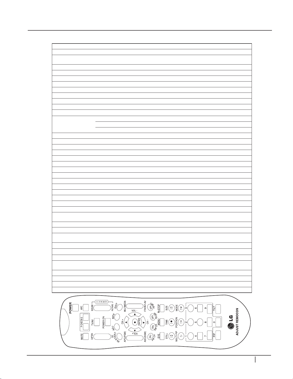
SERVICE REMOTE
NUM KEY FUNCTION
1 POWER To turn the TV on or off
2 POWER ON To turn the TV on automatically if the power is supplied to the TV. Use the POWER key to deactivate; It
3 MUTE To activate the mute function.
4 P-CHECK To check TV screen image easily.
5 S-CHECK To check TV screen sound easily
6 ARC To select size of the main screen (Normal, Spectacle, Wide or Zoom)
7 CAPTION Switch to closed caption broadcasting
8 TXT To toggle on/off the teletext mode
9 TV/AV To select an external input for the TV screen
10 TURBO SOUND To start turbo sound
11 TURBO PICTURE To start turbo picture
12 IN-START To enter adjustment mode when manufacturing the TV sets.
13 ADJ To enter into the adjustment mode. To adjust horizontal line and sub-brightness.
14 MPX To select the multiple sound mode (Mono, Stereo or Foreign language).
15 EXIT To release the adjustment mode.
16 APC(PSM) To easily adjust the screen according to surrounding brightness.
17 ASC(SSM) To easily adjust sound according to the program type.
18 MULTIMIDIA To check component input.
19 FRONT-AV To check the front AV.
20 CH To move channel up/down or to select a function displayed on the screen.
21 VOL To adjust the volume or accurately control a specic function.
22 ENTER To set a specic function or complete setting.
23 PIP CH-(OP1) To move the channel down in the PIP screen. To use as a red key in the teletext mode.
24 PIP CH+(OP2) To move the channel in the PIP screen. To use as a green key in the teletext mode.
25 PIP SWAP(OP3) To switch between the main and sub screens. To use as a yellow key in the teletext mode.
26 PIP INPUT(OP4) To select the input status in the PIP screen. To use as a blue key in the teletext mode.
27 EYE To set a function that will automatically adjust screen status to match. The surrounding brightness so natural
28 MENU To select the functions such as video, voice, function or channel.
29 IN-STOP To set the delivery condition status after manufacturing the TV set.
30 STILL To halt the main screen in the normal mode, or the sub screen at the PIP screen. Used as a hold key in the
31 TIME Displays the teletext time in the normal mode. Enables to select the sub code in the teletext mode.
32 SIZE Used as the size key in the PIP screen in the normal mode. Used as the size key in the teletext mode.
33 MULTI PIP Used as the index key in the teletext mode. Top index will be displayed if it is the top text.
34 POSITION To select the position of the PIP screen in the normal mode. Used as the update key in the teletext mode
35 MODE Used as Mode in the teletext mode.
36 PIP To select the simultaneous screen.
37 TILT To adjust screen tilt.
38 0~9 To manually select the channel.
OVERVIEW
should be deactivated when delivered.
To adjust the screen voltage (automatic): In-start mute Adjust AV (Enter into W/B adjustment mode).
W/B adjustment (automatic): After adjusting the screen W/B adjustment Exit two times
color can be displayed.
teletext mode. Page updating is stopped.
(Text will be displayed if the current page is updated.)
PDP Training - Fall 2008 9
Page 12
OVERVIEW
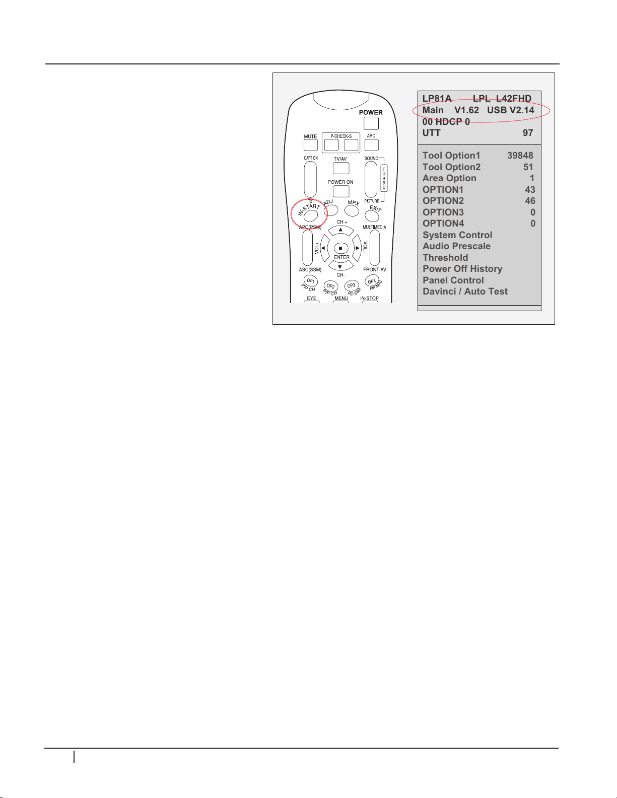
LP81A LPL L42FHD
Main V1.62 USB V2.14
00 HDCP 0
UTT 97
Tool Option1 39848
Tool Option2 51
Area Option 1
OPTION1 43
OPTION2 46
OPTION3 0
OPTION4 0
System Control
Audio Prescale
Threshold
Power Off History
Panel Control
Davinci / Auto Test
LP81A LPL L42FHD
Main V1.62 USB V2.14
00 HDCP 0
UTT 97
Tool Option1 39848
Tool Option2 51
Area Option 1
OPTION1 43
OPTION2 46
OPTION3 0
OPTION4 0
System Control
Audio Prescale
Threshold
Power Off History
Panel Control
Davinci / Auto Test
CHECK FIRMWARE VERSION
You can check the firmware version by
opening the service menu. It is located
near the top of the menu.
UPDATE FIRMWARE
1) Copy the firmware to the top
level on a USB flash drive and to
a folder named LG_DTV. Some
models require the LG_DTV
folder, and some don’t. Put it in
both locations if you are not sure
which is correct. Only copy the
file (or files) for the model you are
currently updating.
2) Turn on the TV and insert the USB
drive to the USB IN port.
3) If the firmware is newer than what is already installed, the upgrade menu should open
automatically. If the update menu doesn’t open, press MENU on the remote and select
OPTION. Now press the 7 key 7 times and the upgrade menu will open.
4) Select START and press ENTER on the remote to start the software upgrade.
5) The TV will copy the update from the drive and then install it. Do not turn the TV off
until it is finished.
6) The TV will automatically turn off and back on after the upgrade is successfully
finished.
7) Check the firmware version to verify the update was succesful.
10 PDP Training - Fall 2008
Page 13
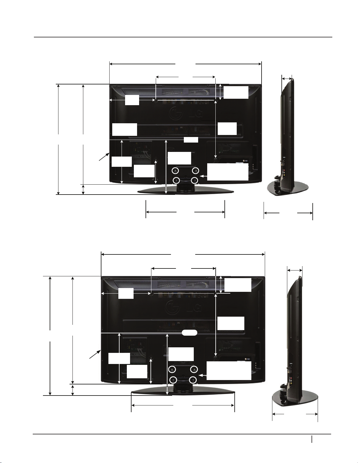
15.8"
400mm
26.7"
678.2mm
6.2"
158mm
40.9"
1038.9mm
28.8"
731.5mm
28.8"
731.5mm
3.4"
86.4mm
12.1"
307.3mm
Center
15.8"
400mm
6.6"
168.78mm
1.93"
49mm
Remove 4 screws to
remove stand for
wall mount
Model No.
Serial No.
Label
15.55"
394.95mm
12.4"
315mm
4.72"
120mm
17.48"
443.95mm
15.8"
400mm
31.1"
789.9mm
15.55"
394.95mm
48.2"
1224.28mm
Remove 4 screws to
remove stand for
wall mount
15.8"
402mm
27.8"
706.1mm
33.4"
848.36mm
3.4"
86.4mm
14.4"
365.76mm
Center
15.8"
400mm
6.69"
170mm
29.72"
759.95mm
2.36"
60mm
8.66"
220mm
Model No.
Serial No.
Label
42PG20 DIMENSIONS
DISASSEMBLY
4
2
P
G
2
50PG20 DIMENSIONS
0
PDP Training - Fall 2008 11
Page 14
DISASSEMBLY
Y-sus & Z-Sus Drive
Control (Logic)
Y-Drive
Voltage Label
Main (Digital)
Panel ID
Power Supply
Z-Sus
Right X-Board
Left X-Board
Side Input
DISASSEMBLY 42PG20
INTRODUCTION
4
2
P
G
2
0
This section of the manual will discuss disassembly of the 42PG20 PDP Direct View
Television. Upon completion of this section the Technician will have a better understanding
of the disassembly procedures, the layout of the printed circuit boards, and be able to
identify each board. The plugs listed are from left to right Pin 1,2, 3, etc. Remember to
be cautious of ESD as many semiconductors are CMOS and prone to static failure.
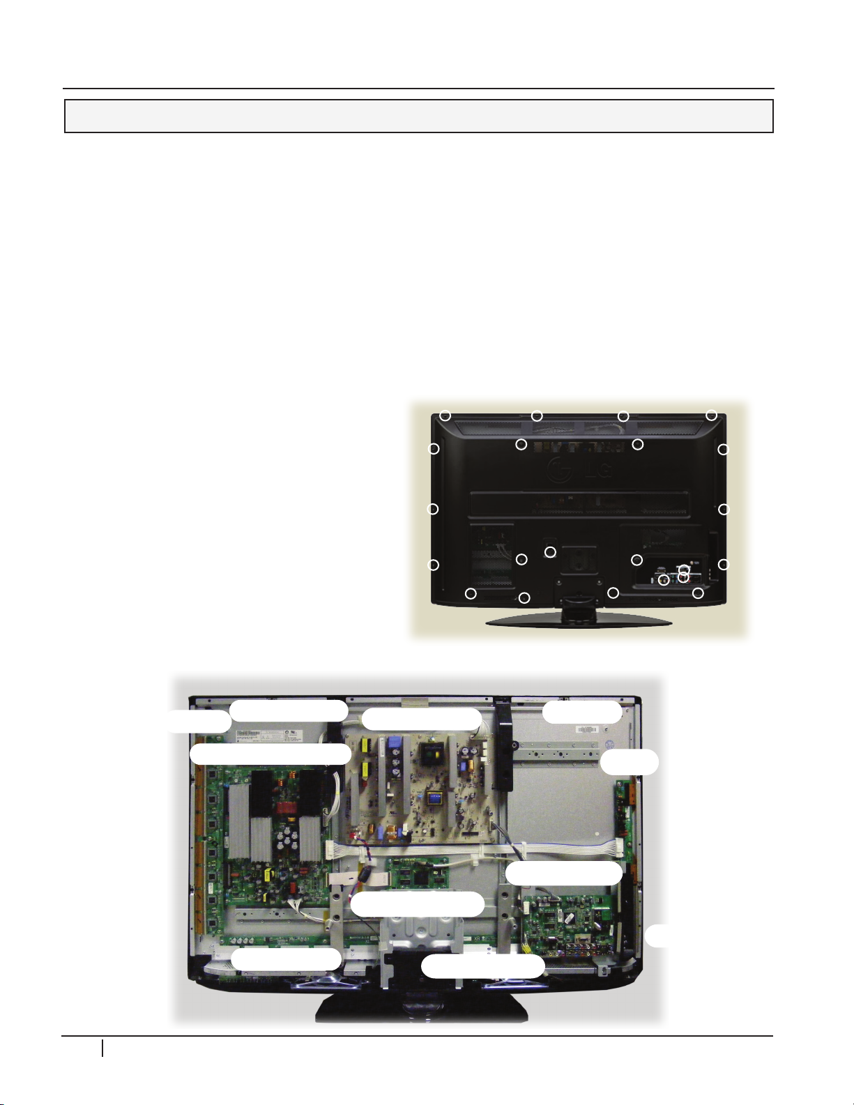
BACK COVER REMOVAL
Remove the 22 screws shown. Pay attention to the size and type of screw as there are
different types. Putting in the improper screw when reassembling may cause damage. The
stand does not need to be removed when removing the back.
BOARD LAYOUT
12 PDP Training - Fall 2008
Page 15

DISASSEMBLY
SWITCH MODE POWER SUPPLY REMOVAL
Disconnect the following connectors: P812, P813, CN101. Remove the 8 screws holding the
board in place. Remove the board. When replacing, be sure to readjust the Va/Vs voltages
in accordance with the Panel Label. Confirm VSC, -Vy and Zbias as well.
Y-SUS BOARD REMOVAL
4
Disconnect the following connectors: P201, P801, P101, P202. Remove the 8 screws
holding the board in place. Remove the board. When replacing, be sure to readjust the
Va/Vs voltages in accordance with the Panel Label. Confirm VSC, -Vy and Zbias as well.
Y-DRIVE BOARD REMOVAL
Disconnect the following Flexible Ribbon Connectors: P1, P2, P3, P4, P5, P6, P7 and
P8. Disconnect the following connectors: P201, P801, P101, P202. Remove the 3 screws
holding the board in place. Remove the board by lifting slightly and sliding the board to
the left unseating P204 and P200. from the Y-Sus board.
Z-SUS BOARD REMOVAL
Remove the support frame holding the Main board. Disconnect the following connectors:
P1, P2 and P3. Remove the 3 screws holding the board in place. Remove the board. When
replacing, be sure to readjust the Va/Vs voltages in accordance with the Panel Label.
Confirm VSC, -Vy and Zbias as well.
MAIN BOARD REMOVAL
Disconnect the following connectors: P701, P302, P303 and JK501. Remove the 2 screws
holding on the decorative plastic piece on the right side. Remove the 4 screws holding
the board in place. Remove the board.
2
P
G
2
0
CONTROL BUTTON BOARD REMOVAL
Disconnect the following connectors: P121, P160, P161 and P162. Remove the 2 screws
holding the board in place. Remove the board. (Note: Power board is behind the Control
board. Remove it’s 2 screws and remove.
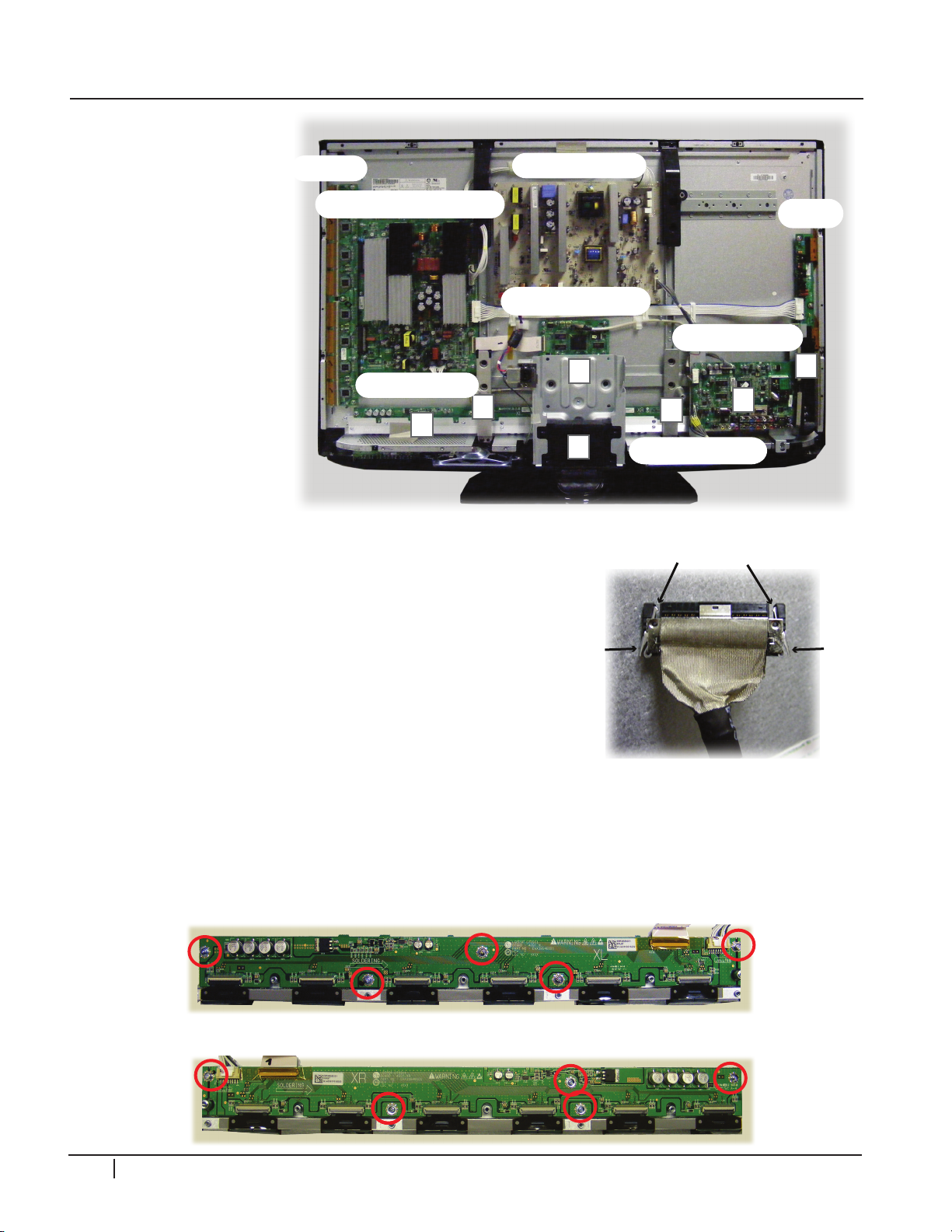
X-DRIVE BOARDS REMOVAL
X-Board Removal will require the most disassembly of all the boards. All the Brackets
and Assemblies marked A-F (Image on next page) will need to be removed including the
Stand. Before an X-Board can be removed. The Heat Sink assembly will also need to be
removed.
Lay the Plasma down carefully on a padded surface. Make sure AC is removed and remove
the back cover and the stand. Carefully remove the LVDS Cable P121 from the Control
board by pressing the Locking Tabs together and pull the connector straight back to
remove the cable. (This prevents damage).
PDP Training - Fall 2008 13
Page 16
DISASSEMBLY
Y-sus & Z-Sus Drive
Control (Logic)
Y-Drive
Main (Digital)
Power Supply
Z-Sus
Right X-Board
Left X-Board
A
F
B
E
E
C
D
A
Locking Tabs
Press In
Press In
Left X-Board
Right X-Board
A) Remove the sStand
mounting support
plastic piece.
4
2
P
G
2
0
B) Remove the stand
m et a l s up p o r t
bracket, unplug AC
ground lug.
C) Remove the 2 screws
from the decorative
black plastic piece
around side input
jacks (Marked B)
and remove.
D) Re m ov e th e 2
screws at the top
of the Main board
Mounting Bracket and peel the tape from the
bottom. Remove connectors P303 and JK501.
Carefully reposition the main board and mounting
bracket up and off to the right side.
E) Remove the metal support brackets marked “E”.
F) Remove the 13 screws holding the heat sink and
carefully lift it straight up and off (remember that
the TCP IC’s are located under the heat sink).
Disconnect all TCP ribbon cables from the defective
X-Drive board and remove the 5 screws holding
the board in place. Reassemble in the reverse order.
Recheck Va/Vs/V-Scan/-VY/Z-Drive.
14 PDP Training - Fall 2008
Page 17
DISASSEMBLY
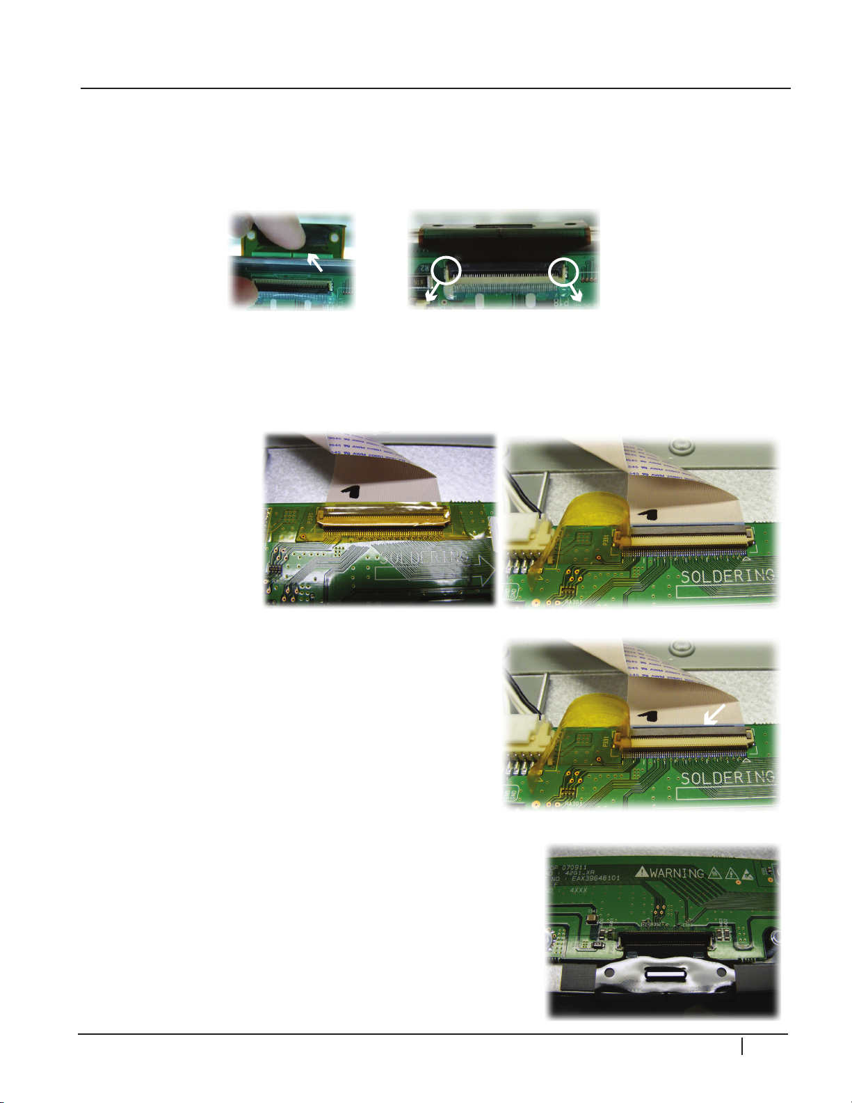
TCP CONNECTOR REMOVAL
Lift up the lock as shown by arrows. (The Lock can be easily broken. It needs to be handled
carefully.) Pull TCP apart as shown by the arrows. The TCP Film can be easily damaged,
handle with care.
P232 & P331 CONNECTOR REMOVAL
The X-Drive boards can be removed after removing the back cover, the main board, and
the heat sink covering the TCPs is removed (15 screws).
Peel the tape off
the connectors and
gently pry the locking
mechanism upward.
4
2
P
G
2
0
Gently pry the locking mechanism upward on all TCP
connectors P201-206 or P301-306.
Carefully lift the TCP ribbon up and off the cushion and
out of the way.
PDP Training - Fall 2008 15
Page 18
4
2
P
G
2
DISASSEMBLY
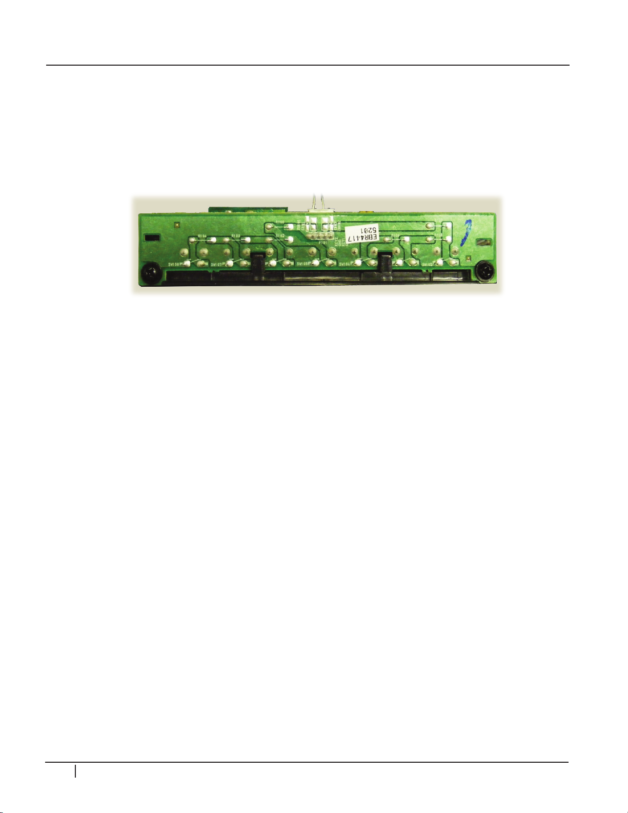
CONTROL BUTTON BOARD REMOVAL
The control button board and power switch board are located in the lower left hand section
(as viewed from the rear).
To remove, unplug the connector P101 and remove the 2 screws. Under each screw there
is a black tab. Release these tabs to lift the board upward. Then remove the connector
from the power switch board and remove it’s two screws.
0
16 PDP Training - Fall 2008
Page 19
300
305
400
203
205
202
240
204
302
200
206
250
201
303
304
306
900
580
560
571
120
561
570
301
260
590
501
270
603
520
602
601
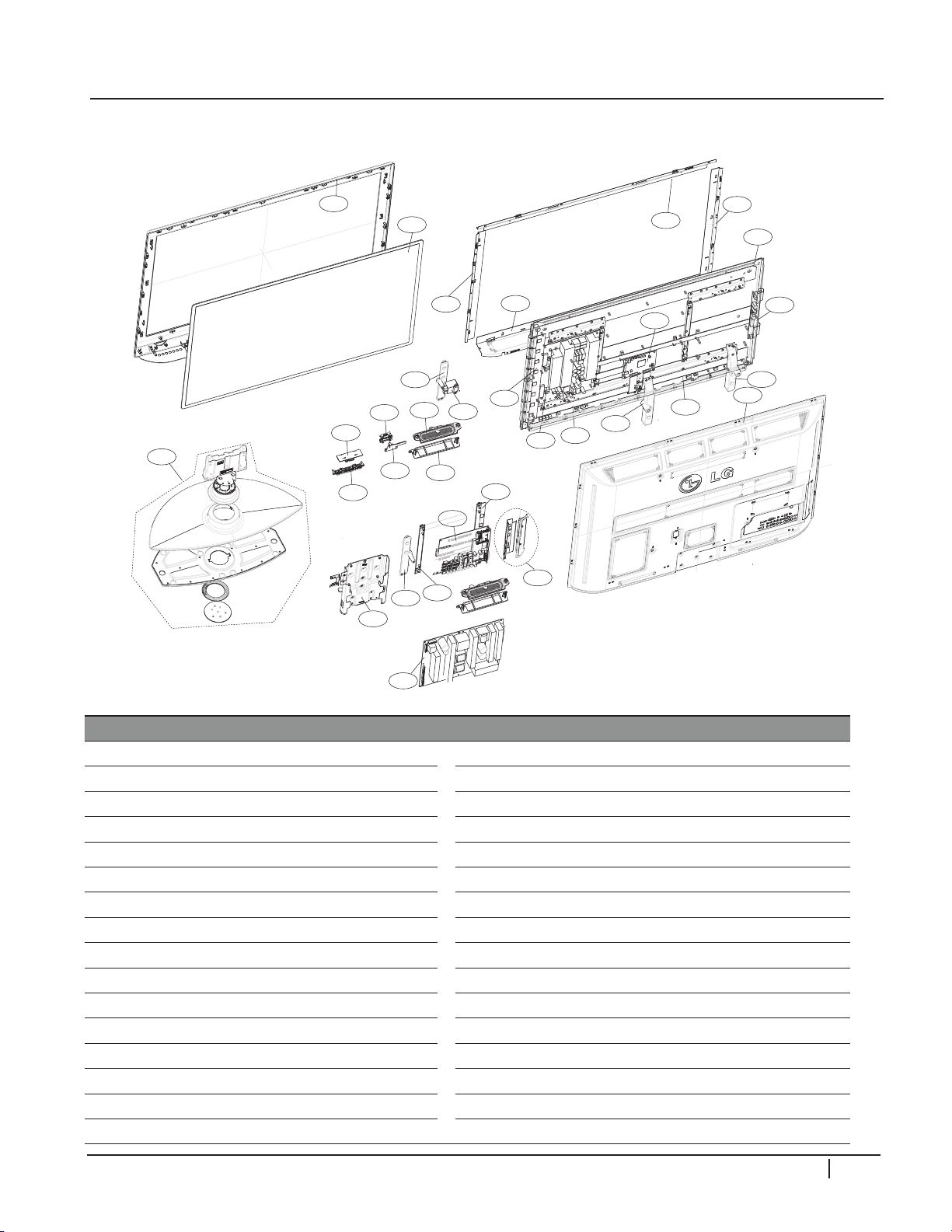
42PG20 EXPLODED VIEW
DISASSEMBLY
4
2
P
G
2
Part numbers subject to change.
Check GCSC (aic.lgservice.com) for
the current part numbers.
Location Part Num Description Location Part Num Description
120 EAB42609901
200 EAJ41970710
201 EBR39594901
202 EBR39712601
203 EBR39595001
204 EBR39595101
205 EBR39706801
206 EBR41668901
240 AJJ35680107
250 AJJ35680108
260 AJJ35680203
270 AJJ35680204
300 ABJ35121812 Front Cabinet 601 ABA35619217
301 ABA36825001 Speaker Bracket Assembly 602 MGJ41163807
302 AJJ35122402
303 AJJ35122502
Full Range Speaker
PDP Panel (PDP Module)
Control board (CTRL)
Y-drive (YDRV)
Left X-Drive (XRLB)
Right X-Drive (XRRB)
Y-Sustain (YSUS)
Z-Sustain (ZSUS)
Top Right Support
Top Left Support
Bottom Right Support
Bottom Left Support
Top Filter Support
Bottom Filter Support
304 AJJ35122602
305 MDJ42350902
306 AJJ35122702 Left Supporter Assembly
400 ACQ35123228 Rear Cover Assembly
501 MGJ41164512 Main Supporter Plate
520 EBR43929102 Hand Insert PCB Assembly,Main
560 EBR43385504
560 EBR48957101
561 MBG41119902
570 EBR44168002
571 ABA36967703 Bracket Assembly
580 EAY43533901
603 MGJ40268206 Side AV Shield
900 AAN35132205
Right Filter Support
Glass Filter
Main/Digital PCB
Sub PCB
Control Buttons
Sub PCB
Power Supply (SMPS)
Side Input Bracket Assembly
Main board Supporter
Stand (Base Assembly)
0
PDP Training - Fall 2008 17
Page 20
4
2
P
G
2
CIRCUIT DESCRIPTIONS
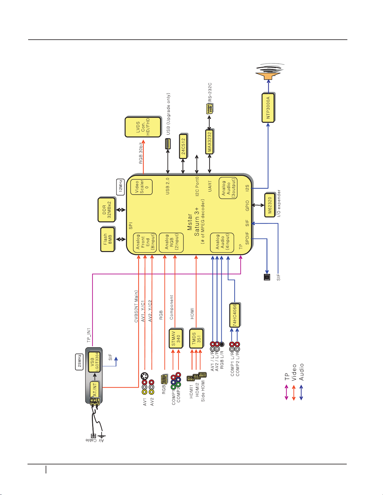
BLOCK DIAGRAM
0
18 PDP Training - Fall 2008
Page 21
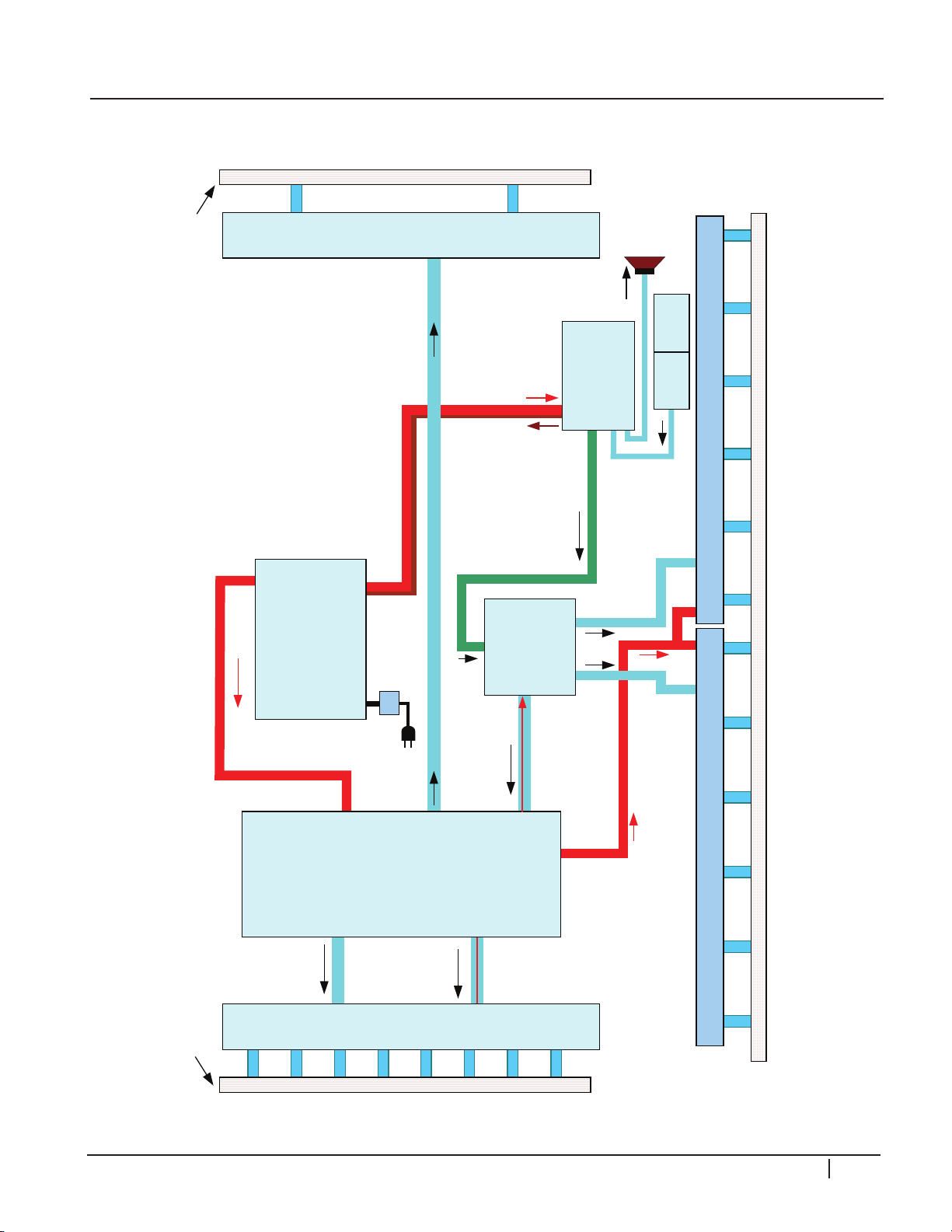
SIGNAL AND VOLTAGE BLOCK DIAGRAM
42PG20 SIGNAL and VOLTAGE DISTRIBUTION DIAGRAM
Display Panel
Horizontal Address
P100
5V
Drive Signal
NEW
Y-SUS
PWB
With Z-Drive
P204
P201
P801
P211
P101
P202
Drive Data
Clock (i2c)
P200
M5V, Va, Vs
P812
P813
CN101
STB +5V, 16V, 5V
SMPS
Turn On
Commands
SMPS
PWB
AC
Input
Filter
NEW
P1
SMPS OUTPUT VOLTAGES
STB +5V, 16V, 5V
Z-SUS
Drive Signals
Logic Signals
P160
AC Voltage
Det
P701
P302
P303
JK501
MAIN
PWB
Speakers
Control
Keys
Power
Keys
X-PWB-Right
X-PWB-Left
P201 P202 P203 P204 P205 P206 P301 P302 P303 P304 P305 P306
RGB Logic Signals
15V, Va
RGB Logic Signals
3.3V
CONTROL
PWB
P162
LVDS
Y Drive PWB
Z SUS PWB
P161
P121
P1 P2 P3 P4 P5 P6 P7 P8
P2P3
Outputs Only
P232
P211 P311 P331
Display Panel Vertical Address
IR
Vs
Display Panel
Horizontal Address
5V
DISASSEMBLY
4
2
P
G
2
0
PDP Training - Fall 2008 19
Page 22
CIRCUIT DESCRIPTIONS
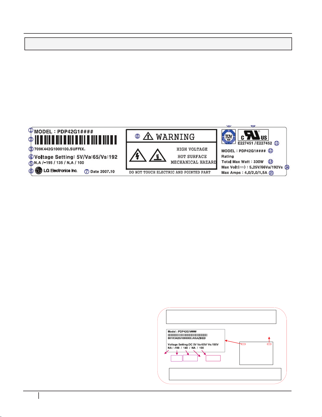
Remember, the Voltage Label MUST be followed,
it is specific to the panel’s needs.
All label references are from a specific panel.
They are not the same for every panel encountered.
-VY
Z_ BIA S
Panel
“Rear View”
Manufacturer
Bar Code
Set-
Up
Ve
Vscan
CIRCUIT DESCRIPTIONS 42PG20
INTRODUCTION
4
2
P
G
2
0
It is critical that the DC Voltage adjustments be checked whenever troubleshooting a
problem. Especially when:
1) The SMPS (Switch Mode Power Supply), Y-Sus (Y-Sustain) or Z-Sus (Z-Sustain)
are replaced.
2) The panel is replaced, since the SMPS does not come with new panel.
3) A picture issue is encountered.
PANEl lAbEl
(1) Model Name
(2) Bar Code
(3) Manufacture No.
(9) TUV Approval Mark
(10) UL Approval Mark
(11) UL Approval No.
(4) Adjusting Voltage DC, Va, Vs
(5) Adjusting Voltage (Set Up/-Vy/Vsc/Ve/Vzb)
(6) Trade name of LG Electronics
(7) Manufactured date (Year/Month)
(8) Warning
ADJUSTMENT ORDER **IMPORTANT**
DC vOlTAGE ADJUSTMENTS
SMPS board: Va Vs (Do SMPS adjustments first)•
Y-Sus board: Adjust Vscan, -Vy•
Y-Sus board: Adjust Zbias •
WAvEFORM ADJUSTMENTS
Y-Sus board: Ramp Up, Ramp Down.
Only necessary when:
1) The Y-Sus board is replaced.
2) “Mal-Discharge” problems.
3) Abnormal picture issues.
20 PDP Training - Fall 2008
(12) Model Name
(13) Max. Watt (Full White)
(14) Max. Volts
(15) Max. Amps
Page 23
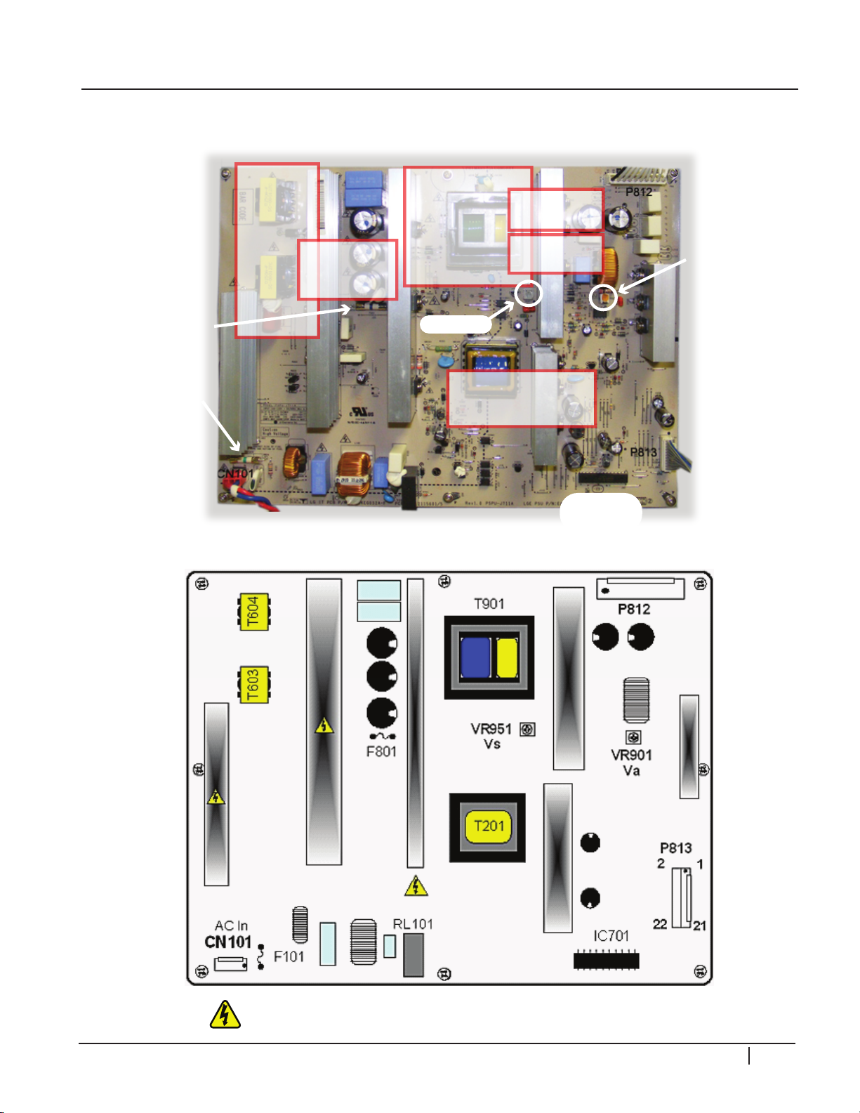
POWER SUPPLY (SMPS)
Hot Ground Symbol represents a SHOCK Hazard
F801
340V Fuse
10Amp/230V
F101
340V Fuse
10Amp/230V
P812
To Y/Z-Sus
Standby
Source
PFC
Circuit
CN 101
AC Input
VS Source
VA Source
IC701
Sub Micon
P813
To Main
VA VR901
380V Source
16V, 12V, 5V, 3.2V
Source
VS VR951
CIRCUIT DESCRIPTIONS
4
2
P
G
2
0
= Shock Hazard
PDP Training - Fall 2008 21
Page 24
4
2
CIRCUIT DESCRIPTIONS
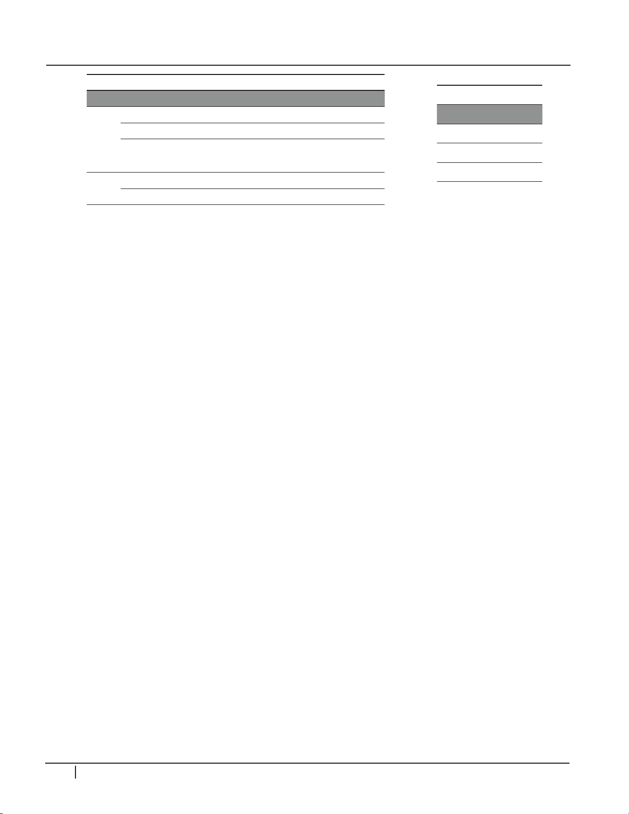
SMPS Outputs
Board Voltage Description
VS Drives the display panel Horizontal Grid
Y-Sus
Main
VA Responsible for display panel Vertical Grid
M5V VCC
16V Audio B+ Supply
5V Control Circuits
Used to develop Bias Voltages on the Y-Sus,
X-Drive, and Control boards
Adjustments
Voltage Location
VA RV901
VS RV951
M5V VCC Fixed
P
G
2
0
POWER SUPPlY OPERATION
Refer to the figures on page 25-27. AC Voltage is supplied to the SMPS board at Connector
CN101 from the AC Input Filter. Standby 5V is developed from 340V source supply
(which during standby measures 159V hot ground). This supply is also used to generate
all other voltages on the SMPS.
The 5V (standby) voltage is routed to the Sub Micon circuit (IC701) on the SMPS and
through P813 to the Main board or Micon (IC100). LD703 will glow green to indicate
STBY 5V has arrived.
AC detect Pin 18 of P813 is generated on the SMPS by monitoring the AC input and
rectifying a small sample voltage. This AC Detect Voltage is routed to IC701 on the Sub
Micon on the SMPS and the Micon (IC100) located on the Main board. It is used as a
basic “SMPS OK” signal.
When the Micon (IC100) on the Main board receives an “ON“ command from either the
keyboard or the Remote IR Signal, it outputs a high to RL-ON. This signal first turns on
a DC level shifter Q706 which creates 5V General. LD703 now glows amber indicating
5V General has been generated. This 5V General now provides the pull up voltages that
supply the output circuits to the SMPS. The RL-ON enters the SMPS board at Pin 19 of
P813. The RL-ON Voltage is sensed by the Sub Micon (IC701) circuit which causes the
Relay Drive Circuit to close Relay RL101. this brings the PFC source up to full power by
increasing the 159V standby to 340V. At this time the 16V source becomes active and
sent to the Main board via P813.
The next step is for the Micon (IC105) on the Main board to output a high on M5V_ON
Line to the SMPS at P813 Pin 21 which is sensed by the Sub Micon IC (IC701) on the
SMPS turning on the 5V VCC line. The last step to bring the supply to “Full Power” occurs
when the Micon (IC100) on the Main board brings the VS-ON line high at Pin 20 of
P813 on the SMPS board which when sensed by the Sub Micon IC (IC701) turns on the
VA and VS Supplies (VA is brought high before VS).
Note: If a voltage is missing, check for proper resistance before proceeding.
22 PDP Training - Fall 2008
Page 25

CIRCUIT DESCRIPTIONS
Understanding the Power On Sequence when Troubleshooting a possible Power Supply
Failure will simplify the process of isolating which circuit board failed to operate properly.
In this Section we will investigate the Power on Sequence and examine ways to locate
quickly where the failure occurred.
Check the Power On LED for Operation. A Red LED indicates a presence of 5V STB and
AC-ON/DETECT. Failure of the Power ON LED to light is an indication of loss of 5V STB
or AC ON/ Detect remember the 5V STB and AC-ON/DETECT are developed on the
SMPS and sent to the Main board. Check LD703 for Green glow.
4
2
When Power is pressed, look for LD703 to change to Amber. Listen for a Relay Click. The
click of the Relay is an indication of RL-ON going high. RL-ON is sent from the Main board
to the SMPS and when present, the IC701 controls the relay operation. RL-ON going High
and no relay is a failure of the SMPS. RL-ON staying low is a failure of the Main board.
Relay Operation means that the SMPS if working properly will output the 16V Supply to
the Main board. This voltage will allow the Tuner, Audio and Video Circuits on the Main
board to function, and if connected to an Antenna Input, Audio would be present. If the
Relays closed and these supplies failed suspect a problem with the SMPS.
The next step of operation calls for the M5V_ON line from the Main board to the SMPS
to go high pin 21 of P813. A high on the M5V_ON line activates the 5V VCC line. Loss
of 5V VCC results in no “Raster”, no Display Panel Reset, no Y, Z, Control or X-board
operation. Loss of 5V VCC and M5V_ON going high could be caused by any of these
boards or failure of the SMPS. M5V_ON staying low indicates a problem on the Main
board.
VS-ON is the last step of the Power Sequence and is responsible for bringing the VS
and VA voltages up. The VS-ON signal pin 20 of P813 is sent from the Main board to
the SMPS as a high, VS and VA and full operation of the Display Panel are now enabled.
Loss of VS-ON results in loss of VA and VS and no Raster, no Panel Display Reset but
audio would be present. If VS-ON went high and VS and VA where missing the problem
P
G
2
0
PDP Training - Fall 2008 23
Page 26
CIRCUIT DESCRIPTIONS
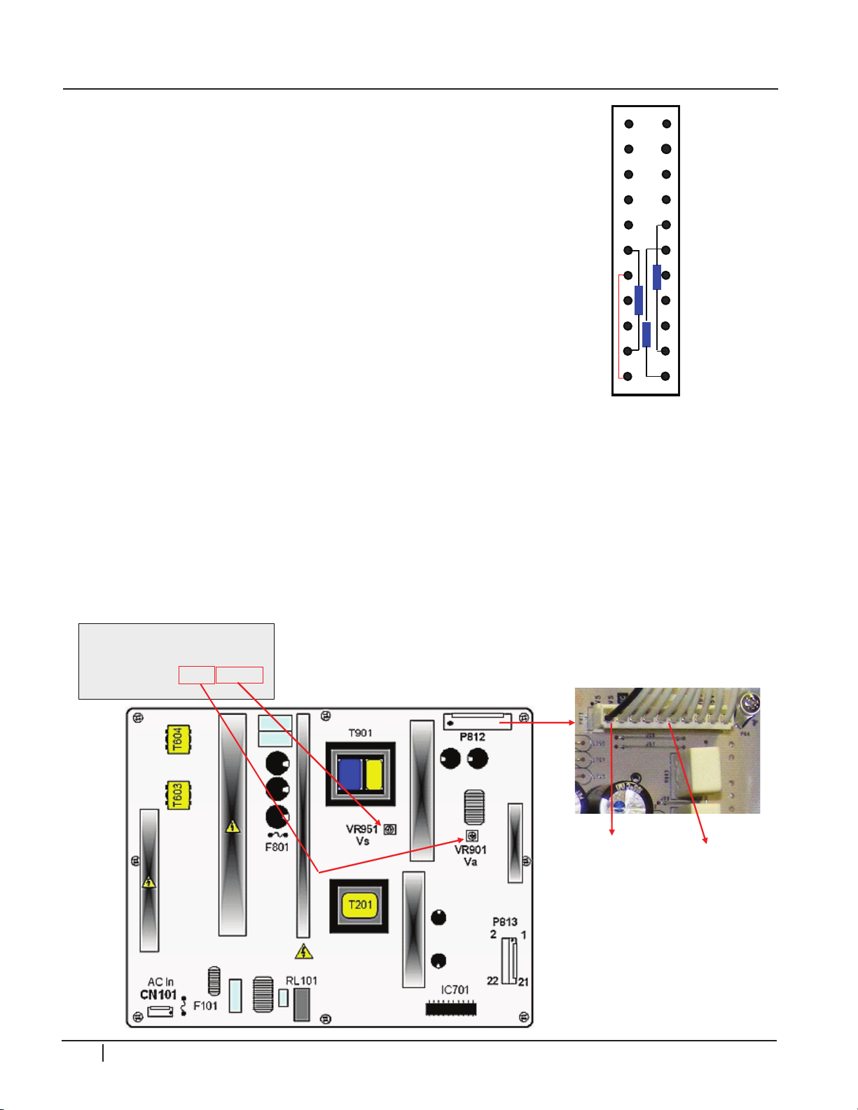
Model : PDP42G1####
||||||||||||||||||||||||||||||||||||||||||||||||||||
801K542 G1008000 .AKAZBED
Voltage Setti ng :DC 5V Va:65 V/ Vs:195 V
NA / -190 / 140 / NA / 100
Vs TP
P812
Pin 1 or 2
Use Full White Raster
Va TP
P812
Pin 5 or 6
2
4
6
8
10
12
14
16
18
22
16V
Gnd
NC
Gnd
5VSTB
5VSTB
Gnd
Gnd
AC Det
VS_ON
Auto Gnd
2
4
6
8
10
12
14
16
18
22
16V
Gnd
NC
Gnd
5VSTB
5VSTB
Gnd
Gnd
AC Det
VS_ON
Auto Gnd
20
3
5
7
9
11
13
15
17
19
21
Gnd
NC
Gnd
5VSTB
5VSTB
Gnd
Gnd
5_V Det
RL_ON
M5V_ON
1
15V
3
5
7
9
11
13
15
17
19
21
Gnd
NC
Gnd
5VSTB
5VSTB
Gnd
Gnd
5_V Det
RL_ON
M5V_ON
1
15V
could be caused by a failure on the SMPS or a circuit
using these voltages. A resistance check should narrow
the possible failures quickly.
4
2
P
G
2
0
POWER SUPPlY STATIC TEST
This test can confirm the proper operation of the SMPS
without the need to exchange the board.This Power
Supply can operate in a No Load State. This means that
by applying AC power to SC101 and all other plugs
disconnected, this power supply will function. Simply
removing P813 (Lower Right Hand Side of the board),
will cause the “AUTO” Pin 22 to go high from its normal
low state allowing the Power Supply to go to full power
on mode when AC Power is Supplied. Be careful after this
test and make sure the VA and VS lines have discharged before reconnecting the supply
cables.
If the Y-Sus and Z-Sus boards are working normal, “Display Panel Reset” will be visible
when the SMPS comes up to full power. Shorting the Auto Pattern Gen. test points at
this time should result in test patterns on the screen.
vS/vA ADJUSTMENTS
This Power Supply will come up and run with “no” load (P812 pulled). Pull P813, apply AC
power, and the Power Supply starts. Y-Sus/Z-Sus runs “Yes” both Y and Z waveforms.
24 PDP Training - Fall 2008
Page 27
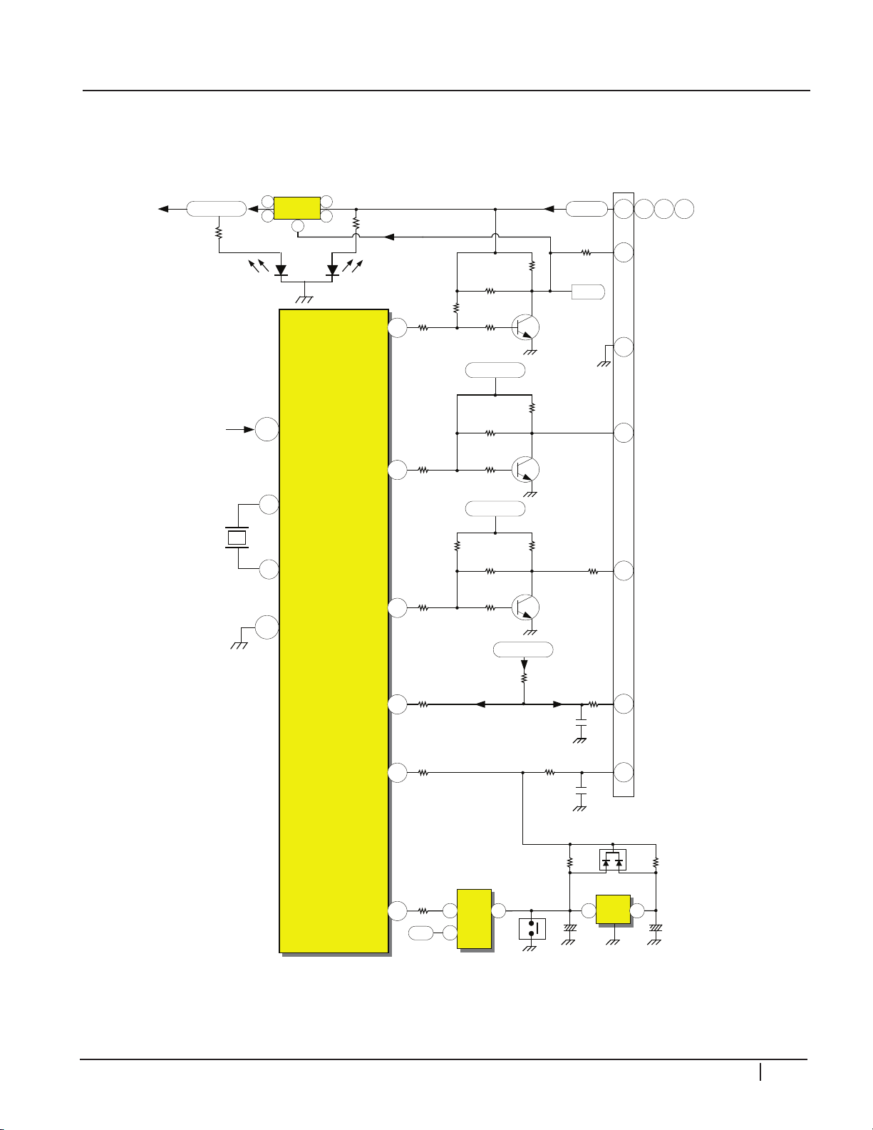
42PG20 Power Supply Controls from Micro Side
76
Pulse
R1045
RL-ON
Pull-Down
Va/Vs-On
166
Pull-Down
R137
M5V-On
115
INT
R184
AC-DET
AC-DET
I
O
1
1A
2
1Y
14
3.3V
128
HW-RESET
P701
18
R727
R764
R717
R723
R718
R715
19
R763
RL-ON
R711
R6070
R716
+5V-General
21
0ohm
RL-ON
M5V-On
AC-DET
VS-On
80
Pull-Up
R126
5V-MNT
17
5V-DET
R722
R720
R142
R141
C142
C143
68010K
SW100
Vcc
R135
167
R136
R732
R736
R729
20
0ohm
Q704
R6071
+5V-General
+5V-General
Q702
C713
Q703
C701
IC101
D100
IC104
254
255
X100
12Mhz
Vcc
9
10
11
12
+5V-ST
Level Shifter
LD703
Set Off +5VST Red
Set On 5VGen Amber
22
Gnd
Q706
+5V-General
4
6
5
RL-ON
LD703
1.8V
1.6V
IC100
RedGreen
3
2
MICRO POWER SUPPlY CONTROl
CIRCUIT DESCRIPTIONS
4
2
P
G
2
0
PDP Training - Fall 2008 25
Page 28
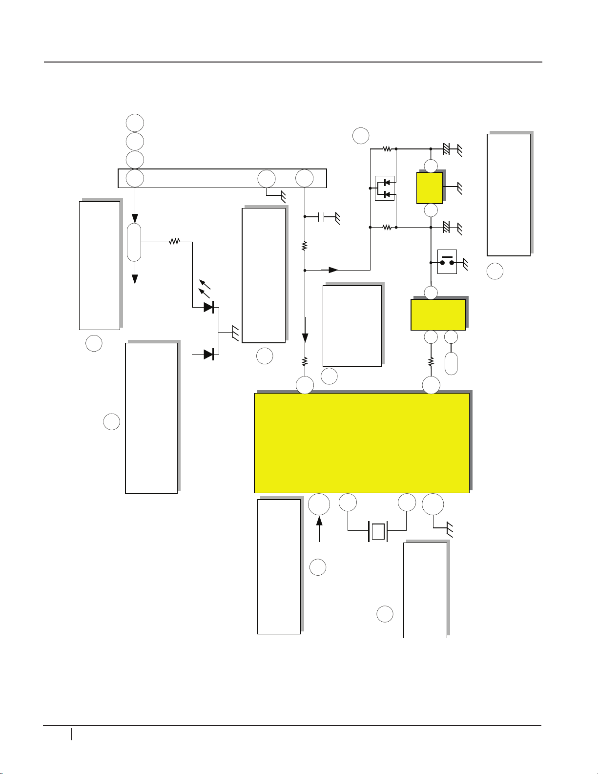
4
42PG20 Power Supply Controls from Micro Side 1
st
STEP
115
INT
R184
AC-DET
AC-DET
IO1
1A
2
1Y
14
3.3V
128
HW-RESET
P701
18
R727
AC-DET
R142
R141
C142
C143
68010K
SW100
Vcc
R135
C713
IC101
D100
IC104
254
255
X100
12Mhz
Vcc
9 10 11 12
Gnd
22
IC100
+5V-ST
RL-ON
LD703
1.8V
Green
5V-SBY Arrives
from SMPS
AC-DET Arrives
from SMPS
Micro Receives Vcc
AC-DET creates
Micro Reset
Oscillator
starts
LED703 receives
5VST and glows Green
A
B
B
A
A
D
A
C
SW 100 Manual
Micro. Reset
AC-DET is
Monitored
by uP
2
P
G
2
0
CIRCUIT DESCRIPTIONS
MICRO POWER SUPPlY CONTROl - STEP1
26 PDP Training - Fall 2008
Page 29
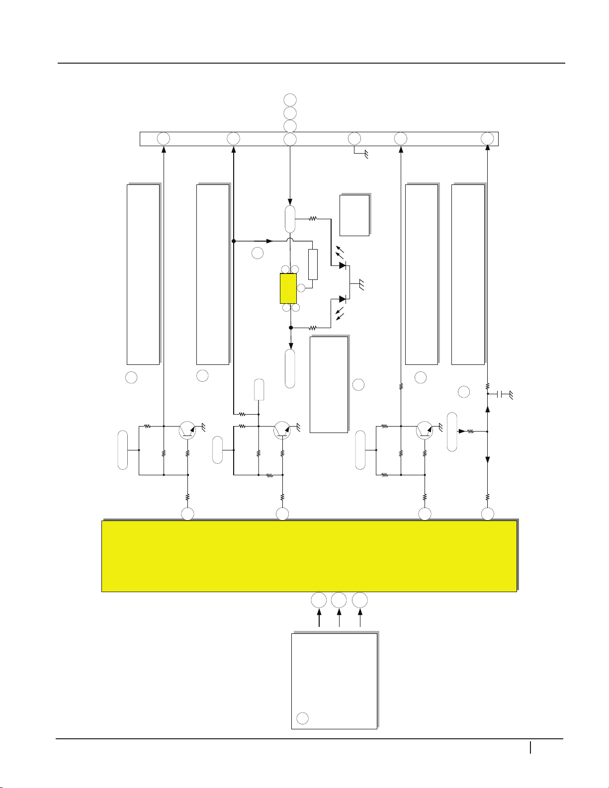
P701
118
9
10
11
12
+5V-ST
Q706
+5V-General
Level Shifter
4
6
LD703
1.8V1.6V
Red
5
42PG20 Power Supply Controls from Micro Side 2
nd
STEP
119
KEY
CONTROLS
IC100
114
REMOTE
IR In
R764
VS-On
80
Pull-Up
R126
5V-MNT
17
5V-DET
R722
R720
167
R136
R732
R736
R729
20
0ohm
Q704
R6071
+5V-General
+5V-General
C701
Green
Appears Amber
166
R137
M5V-On
R711
R6070
R716
+5V-General
21
0ohm
M5V-On
Q702
76
Pulse
R1045
RL-ON
R717
R723
R718
R715
+5V-ST
19
R763
RL-ON
RL-ON
Q703
22
RL-ON
To other
circuts
Receives
Power On
Command
From Side Keys or
Remote
Outputs Relay On (RL-ON) command
Turns on Power Supply Relay
Turns on Q706
Creates 5V General
Lights
Amber
Outputs M5V On command
Turns on 16V/12V Power Supplies
5V General allows 5V Detect
To be Generated
Outputs VS-On which turns on Va and
Vs in the Power Supply
A
E
B
D
F
C
B
3
2
MICRO POWER SUPPlY CONTROl - STEP2
CIRCUIT DESCRIPTIONS
4
2
P
G
2
0
PDP Training - Fall 2008 27
Page 30
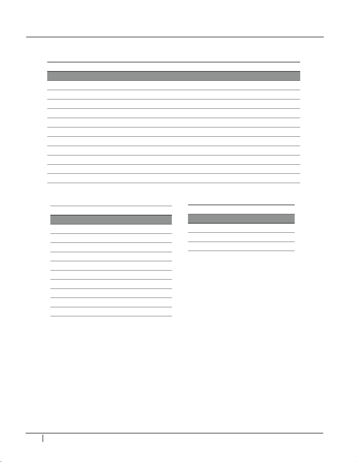
4
2
P
G
2
CIRCUIT DESCRIPTIONS
PIN vOlTAGES
P701 “Main” to P813 “SMPS”
Pin Label STBY Run No Load Diode Pin Label STBY Run No Load Diode
1 15V 0V 16.5V
3 Gnd Gnd Gnd
5 NC NC NC
7 Gnd Gnd Gnd
9 5V 5V 5V
11 5V 5V 5V
13 Gnd Gnd Gnd
15 Gnd Gnd Gnd
17 5_V Det .15V 5V
19 RL_On 0V 3.73V
21 M5V_ON 3.27V 3.24V
16.5V
Gnd
NC
Gnd
5V
5V
Gnd
Gnd
5V
0V
0V
3.8V 2 15V 0V 16.5V
Gnd 4 Gnd Gnd Gnd
Open 6 NC NC NC
Gnd 8 Gnd Gnd Gnd
0.75V 10 5V 5V 5V
0.75V 12 5V 5V 5V
Gnd 14 Gnd Gnd Gnd
Gnd 16 Gnd Gnd Gnd
3.25V 18 AC Det 5V 5V
Open 20 Vs_On 0V 3.2V
1.22V 22 AUTO Gnd Gnd
16.5V
Gnd
NC
Gnd
5V
5V
Gnd
Gnd
5V
0V
5V
2.82V
Gnd
Open
Gnd
0.75V
0.75V
Gnd
Gnd
Open
1.22V
Gnd
0
P812 “Power Supply” to P201 “Y-Sus”
Pin Label Standby Run Diode Mode
1 Vs 0V *194V Open
2 Vs 0V *194V Open
3 NC NC NC NC
4 Gnd 0V 0V Gnd
5 Gnd 0V 0V Gnd
6 Va 0V *65V Open
7 Va 0V *65V Open
8 Gnd 0V 0V Gnd
9 M5V 0V 5V .83V
10 M5V 0V 5V .83V
CN101 “Power Supply” from AC In
Pin Standby Run Resistance
1 120VAC 120VAC 480K
2 N/C - -
3 120 VAC 120VAC 480K
28 PDP Training - Fall 2008
Page 31
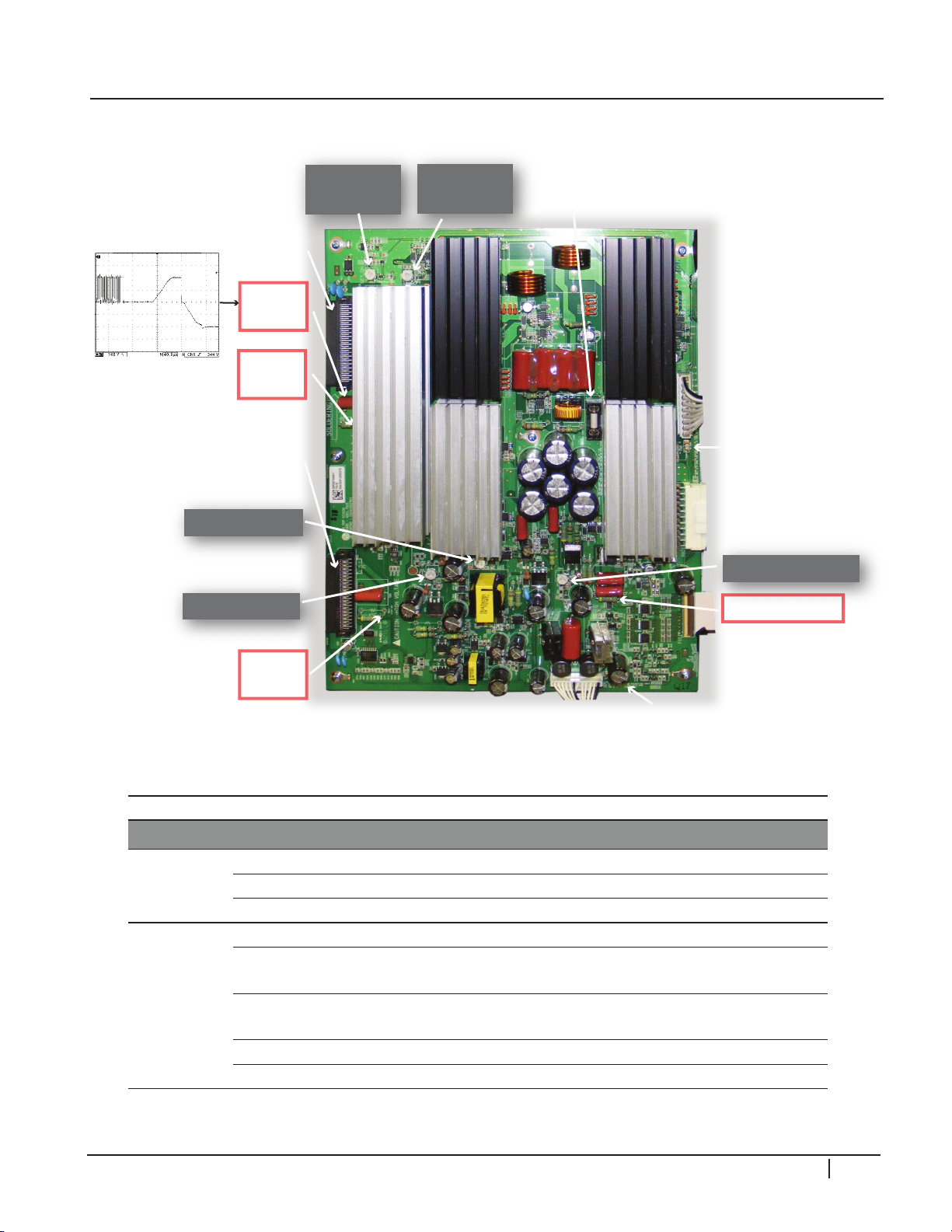
Y-SUS BOARD
VR602
V-Set Up
P204
To Y-Drive
VR601
V-Set Down
C221
Drive TP
VSC ADJ VR501
P200
To Y-Drive
R210
-VY TP
R211
VSC TP
-VY ADJ VR502
FS201
5A
Z-Bias ADJ VR905
P101
Logic Signals
From Control
Z-Bias TP R496
P801
Z-Drive to
Z output
P201
Vs & Va
From SMPS
FS701 (Va)
10A
P202
FS202 (Vs)
4A 250V
CIRCUIT DESCRIPTIONS
4
2
P
G
2
Board Voltage
SMPS
Developed on
Y/Z-Sus
VS Supplies the Horizontal Grid
VA Supplies the Vertical Grid
VCC 5V 5V Supplies Bias to Y/Z-Sus, Control, and X-Boards
-VY -VY Sets the Negative excursion of the Y SUS Drive Waveform
V-Set Up
VR602
V-Set Down
VR601
16V To the X-Drives and TCP ICs
VSC VSC Set the amplitude of the complex waveform
Ramp UP sets Pitch of the Top Ramp of the Drive Waveform
V Set Down sets the Pitch of the Bottom Ramp of the Drive Waveform
SMPS Outputs
0
PDP Training - Fall 2008 29
Page 32
4
30F122
Forward 0.5V ~ 0.7V
Reverse: OL
30F122
Forward 0.4V ~ 0.5V
Reverse: OL
RF2001
Forward 0.3V ~ 0.5V
Reverse: OL
RF2001
Forward 0.3V ~ 0.5V
Reverse: OL
45F123
Forward 0.3V ~ 0.5V
Reverse: OL
45F123
Forward 0.9V ~ 1.0V
Reverse: OL
VR502
Model : PDP42G1####
||||||||||||||||||||||||||||||||||||||||||||||||||||
801K542G1008000 .AKAZBED
Voltage Setting :DC 5V Va:65V/ Vs:195V
NA / -190 / 140 / NA / 100
VSC
-VY
Model : PDP42G1####
||||||||||||||||||||||||||||||||||||||||||||||||||||
801K542G1008000 .AKAZBED
Voltage Setting :DC 5V Va:65V/ Vs:195V
NA / -190 / 140 / NA / 100
VSC
-VY
Lower Left
Side of Y-Sus
VSC TP
-Vy TP
VR501
Lower Left
Side of Y-Sus
Middle Left
Side of Y-Sus
R210
R211
+
-
+
-
2
P
G
2
CIRCUIT DESCRIPTIONS
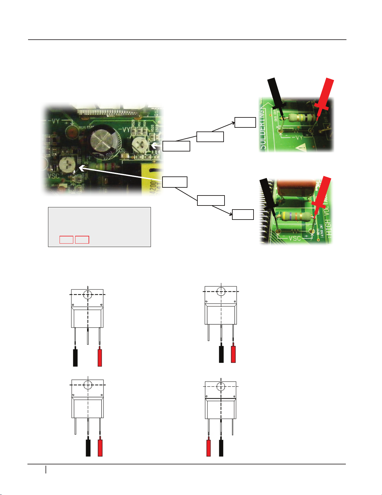
vSC AND -vY ADJUSTMENTS
Set should run for 15 minutes, this is the “Heat Run” mode. Set screen to White Wash
mode or 100IRE White input. Adjust –Vy to 190V (+/- 1V). Adjust VSC to 140 (+/1V).
0
Y-SUS OUTPUT FETS
-
+
+-
30 PDP Training - Fall 2008
+-
+ -
Page 33
CIRCUIT DESCRIPTIONS
0V
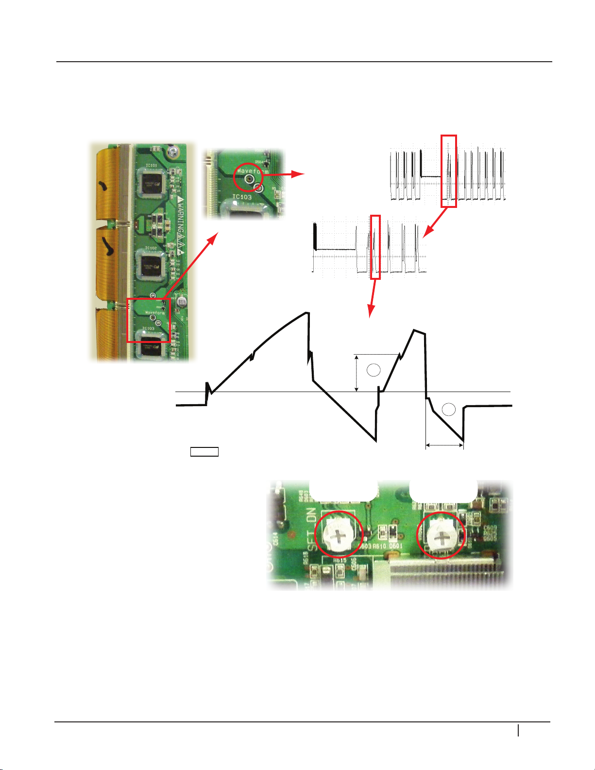
A) Observe the
Ramp Up portion
A
Y Setup Ramp VR602
150V p/p
+/- 5V
Y Drive PWB
Waveform Test Point
B
B) Observe the
Ramp Down
“Time” portion
Y Setup Ramp
VR601
110 us
+/- 5us
2
nd
Pulse
100us
2.00ms
100V per division
1.00ms
100V per division
V-Set Down
VR601
V-Set Up
VR602
Upper left side of the Y-Sus board
v-SET UP AND v-SET DOWN ADJUSTMENTS
VSC and –VY Must have already been completed. Observe the Picture while making these
adjustments. Normally, they do not have to be done.
4
2
P
G
2
0
PDP Training - Fall 2008 31
Page 34
4
FIG1
FIG2
FIG3
Area to
be adjusted
Area to
be adjusted
Zoomed out
Area to
be adjusted
Outlined
Area
FIG4
FIG5
FIG6
Area to
be adjusted
Area to
be adjusted
Area to
be adjusted
Zoomed out
Outlined
Area
2
P
CIRCUIT DESCRIPTIONS
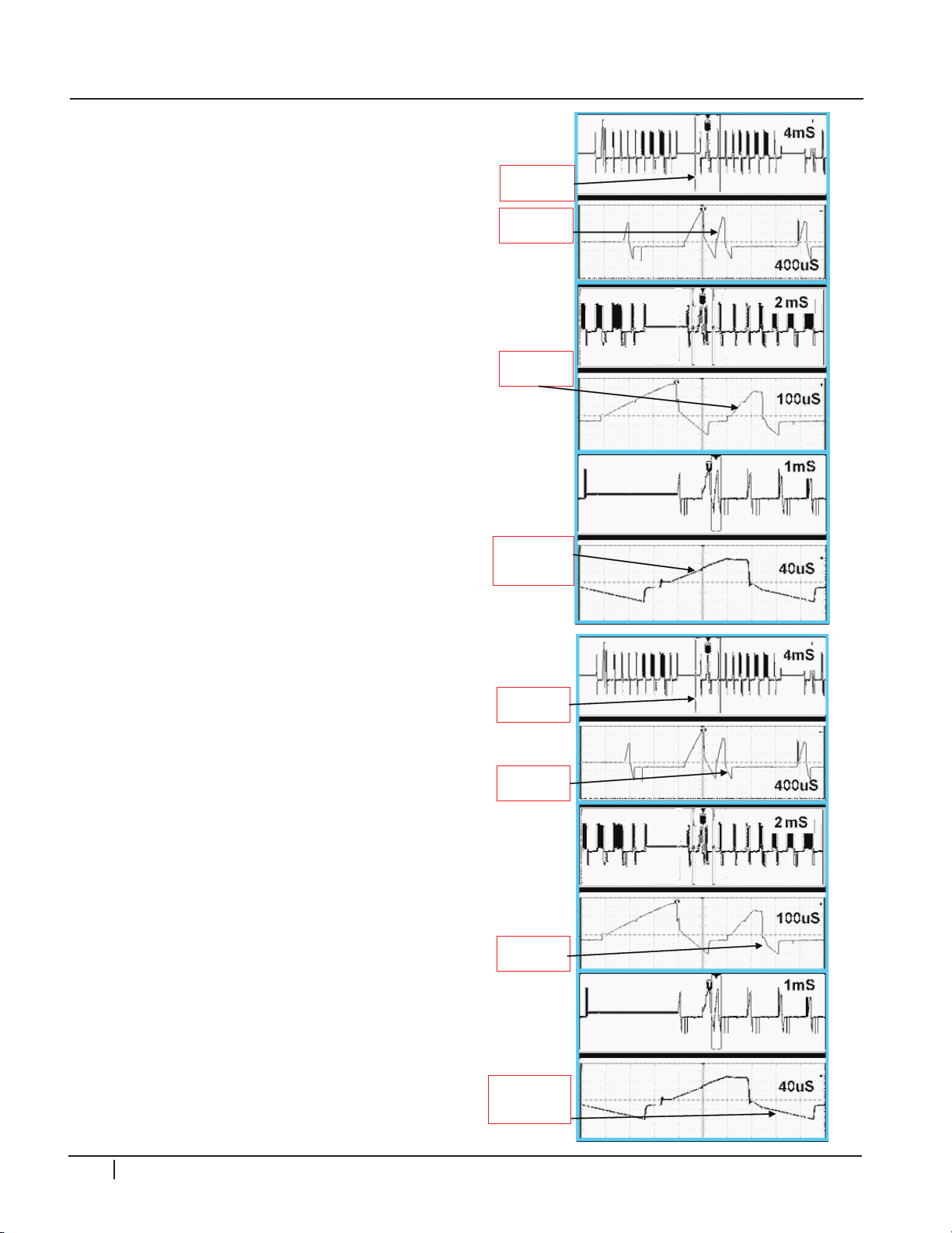
v-SET UP AND v-SET DOWN ADJUSTMENTS
Fig1 top shows the Y-Drive Waveform signal
locked in at 4ms per/div. The signal for Vsetup
is outlined within the Waveform.
At 400uSec per/division, the Fig1 lower
waveform shows Vsetup isolated.
Fig2 top is 2ms per/division. The signal for
Vsetup is now easier to recognize and is
outlined within the Waveform.
G
2
0
At 100uSec per/division, the Fig2 lower
waveform shows Vsetup isolated.
At 1ms per/division, the signal for Vsetup is
now clearly visible. It is outlined within the Fig
3 top waveform.
At 40uSec per/division in Fig3 lower, the
adjustment for Vsetup can be made.
Fig4 top shows the signal locked in at 4ms
per/div and the outlined signal for Vsetdn.
At 400uSec per/division, Fig4 lower waveform
shows Vsetdn isolated.
At 2ms per/divison as in Fig5 top, the outlined
signal for Vsetdn is now easier to recognize.
At 100uSec per/division, Fig5 lower waveform
shows Vsetdn isolated.
At 1ms per/division the outlined signal for
Vsetdn is now clearly visible in Fig6 top.
At 40uSec per/division as in Fig6 lower, the
adjustment for Vsetdn can be made.
32 PDP Training - Fall 2008
Page 35
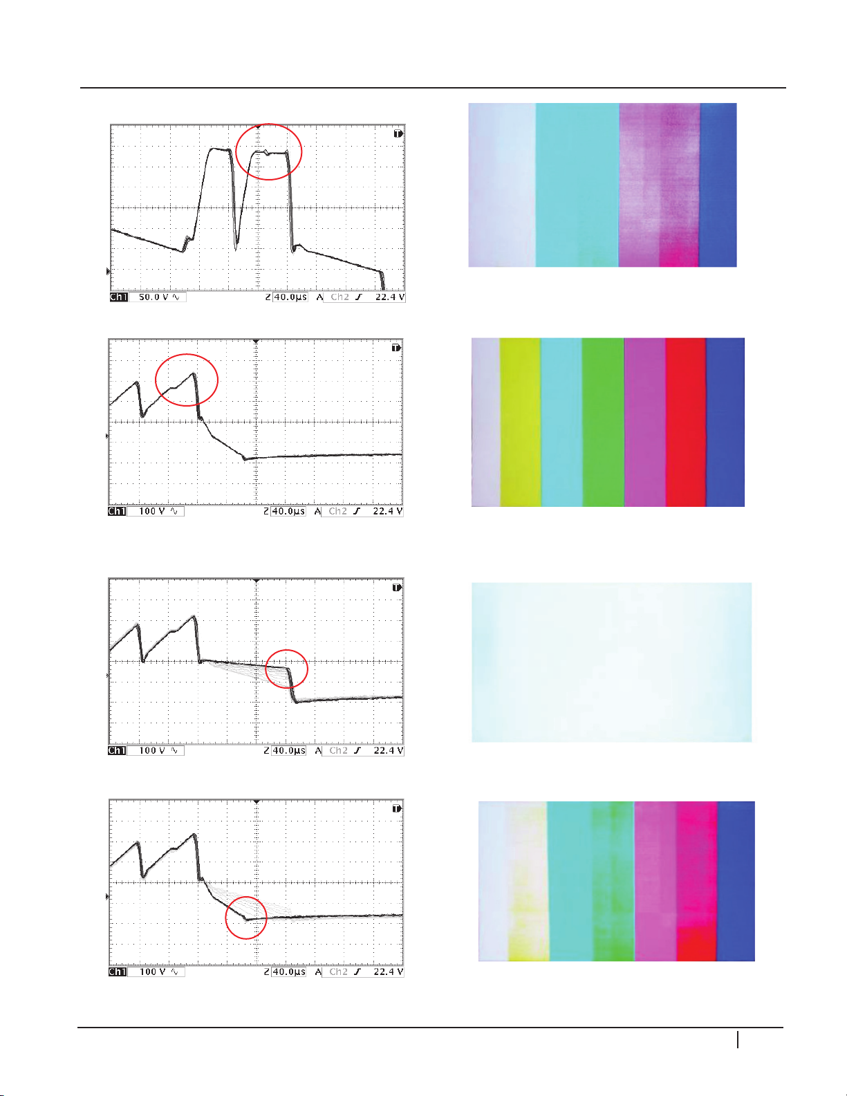
v-SET UP TOO hIGh OR lOW
V-Set Up Too High
CIRCUIT DESCRIPTIONS
The center begins to wash out and arc due to Vset UP
peeking too late and alters the start of the Vset DN
phase.
4
2
P
G
2
V-Set Up Too Low
v-SET DOWN TOO hIGh OR lOW
V-Set Down Too High
0
Very little alteration to the picture, the wave form
indicates a distorted Vset UP. The peek widens due to
the Vset UP peeking too quickly.
All of the center washes out due to increased Vset_DN
time.
V-Set Down Too Low
The center begins to wash out and arc due to decreased
Vset DN time.
PDP Training - Fall 2008 33
Page 36
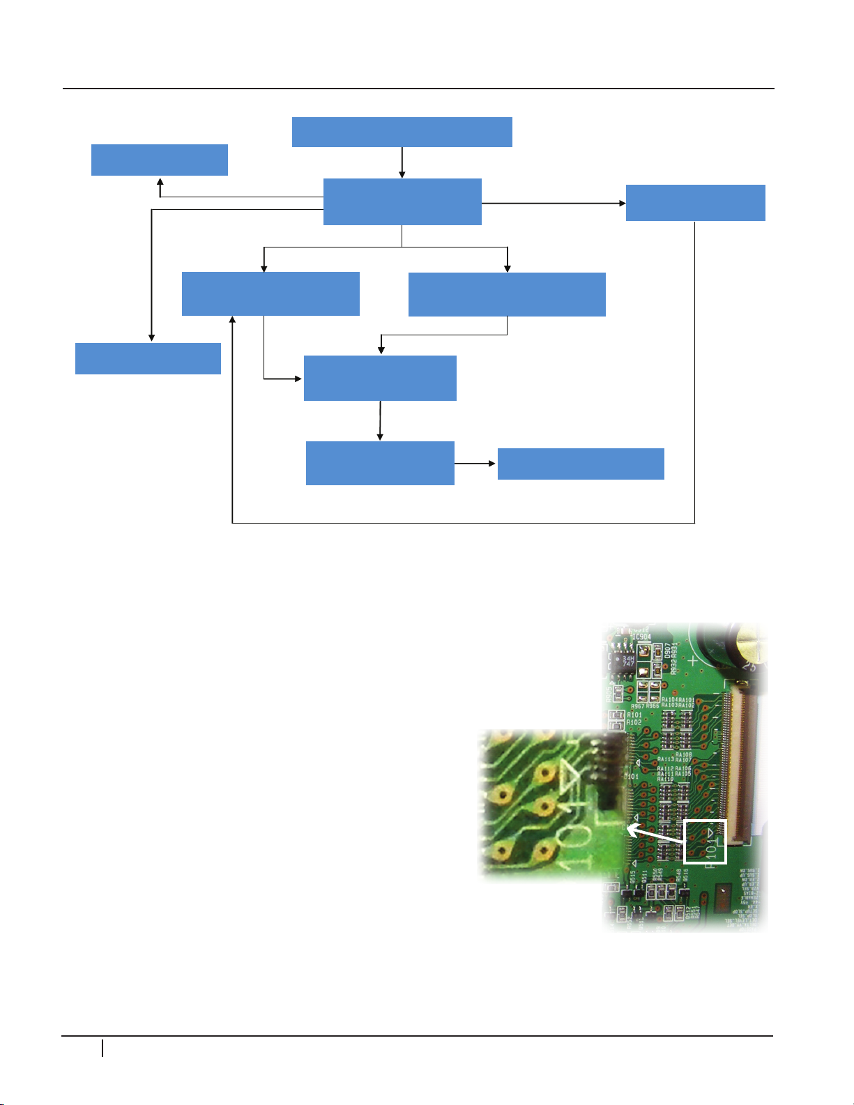
4
Y-Sus P101
Generates Vsc, -Vy and V Set Up
from Vs by DC/DC Converters
Control Board
Circuits generate
Y Sustain Waveform
Distributes 5V VS
Distributes 5V
Logic signals
needed to
generate drive
waveform
Distributes 16V VA
Receive 5V VCC, Va, Vs
from SMPS
Transfer Waveform
to Y Drive Board
Z SUS Section on the
Same PWB
Left/Right X Board
Display Panel
Power Supply Board - SMPS
FETs amplify Sustain
Waveform
2
P
G
2
CIRCUIT DESCRIPTIONS
Y-SUS blOCk DIAGRAM
0
Y-SUS P101 TO CONTROl P160
These connector pins are too close to read
without possible damage to the board. It’s a
60 Pin connector but only has labels 1-19
on the Control board. Looking closely, these
test points are “every other pin”. The bottom
TP represents the “19” label on the Control
board. Pin 1 on the Y-Sus board is actually pin
60 on the Control board side. Take resistance
readings with the board disconnected using the
Diode mode on a digital volt meter. However,
this connector has many more pins than shown
on the Control board Labeling. Roughly 39 pins
34 PDP Training - Fall 2008
Page 37
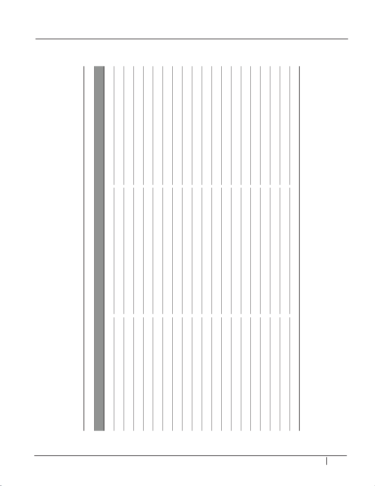
CIRCUIT DESCRIPTIONS
4
2
P
G
2
P101 “Y-Sus” to P160 “Control”
0
2 CLK 0V 3.2V 2.87V 22 Set_DN2 0V 0.2V 2.87V 42 5V OV 4.75V 0.76V / (1.7K)
1 Gnd Gnd Gnd Gnd 21 Gnd Gnd Gnd Gnd 41 5V OV 4.75V 0.76V / (1.7K)
Pin Label STBY Run Diode Mode Pin Label STBY Run Diode Mode Pin Label STBY Run Diode Mode
5 Gnd Gnd Gnd Gnd 25 Gnd Gnd Gnd Gnd 45 n/c n/c n/c n/c
4 STB 0V 0.76V 2.87V 24 PASS_TOP 0V 0.2V 2.87V 44 5V OV 4.75V 0.76V / (1.7K)
3 Gnd Gnd Gnd Gnd 23 Gnd Gnd Gnd Gnd 43 5V OV 4.75V 0.76V / (1.7K)
6 OSC1 0V 0V 2.87V 26 DELTA_Vy 0V 0.16V 2.87V 46 n/c n/c n/c n/c
7 Gnd Gnd Gnd Gnd 27 Gnd Gnd Gnd Gnd 47 Z-ENABLE 0V 0V 1.25V
8 OSC2 0V 3V 2.87V 28 DET_LEVEL 0V 0V 2.87V 48 Gnd Gnd Gnd Gnd
9 Gnd Gnd Gnd Gnd 29 Gnd Gnd Gnd Gnd 49 Z-BIAS 0V 1.71V 1.1V
10 D ATA 0V 0.6V 2.87V 30 SLOPE_RETE 0V 0V 2.87V 50 Gnd Gnd Gnd Gnd
11 Gnd Gnd Gnd Gnd 31 Gnd Gnd Gnd Gnd 51 VZB-SEL 0V 0V 1.1V
12 SUS_DN 0V 0V 2.87V 32 SET_UP 0V 1.9V 2.87V 52 Gnd Gnd Gnd Gnd
13 Gnd Gnd Gnd Gnd 33 Gnd Gnd Gnd Gnd 53 Z-ER_UP 0V 1.25V 1.1V
14 SUS_UP 0V 2V 2.87V 34 Set_DN_2 0V 1.4V 2.87V 54 Gnd Gnd Gnd Gnd
15 Gnd Gnd Gnd Gnd 35 Gnd Gnd Gnd Gnd 55 Z-ER_DN 0V 1.35V 1.1V
20 SET_UP 0V 0.26V 2.87V 40 5V OV 4.75V 0.76V / (1.7K) 60 Gnd Gnd Gnd Gnd
19 Gnd Gnd Gnd Gnd 39 n/c n/c n/c n/c 59 Z-Sus_DN 0V 1.15V 1.1V
18 ER_UP 0V 2V 2.87V 38 Y-Enable 0V 0.6V 2.87V 58 Gnd Gnd Gnd Gnd
17 Gnd Gnd Gnd Gnd 37 Gnd Gnd Gnd Gnd 57 Z-Sus_UP 0V 0.35V 1.1V
16 ER_DN 0V 1.2V 2.87V 36 X_ER 0V 2.9V 2.87V 56 Gnd Gnd Gnd Gnd
PDP Training - Fall 2008 35
Page 38
4
P204
To Y-Drive
P101
Logic Signals
From Control
P801
Z-Drive to
Z output
P201
Vs & Va
From SMPS
P202
P200
To Y-Drive
2
P
G
2
CIRCUIT DESCRIPTIONS
Y-SUS CONNECTIONS
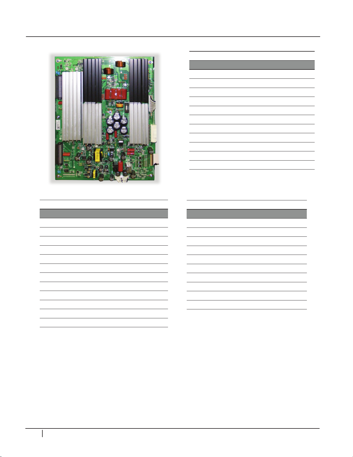
“Y-Sus” P801 to “Z-Drive” P1
Pin Label Standby Run Diode Mode
1 +Vs 0V *194V Open
2 Gnd Gnd Gnd Gnd
3 ZSUS 0V 70.46V Open
4 Gnd Gnd Gnd Gnd
5 ZSUS 0V 70.46V Open
6 Gnd Gnd Gnd Gnd
7 ZSUS 0V 70.46V Open
8 Gnd Gnd Gnd Gnd
9 ZSUS 0V 70.46V Open
10 Gnd Gnd Gnd Gnd
11 ZSUS 0V 70.46V Open
Note: Voltages will vary in accordance with Panel
Label
0
P202 “Y-Sus” to “X-Drive Left” P242
Pin Label Standby Run Diode Mode
1 Gnd Gnd Gnd Gnd
2 Gnd Gnd Gnd Gnd
3 15V 0V 15.8V 1V
4 ER2 0V 61.5V Open
5 ER2 0V 61.5V Open
6 Va 0V 64.9V Open
7 Gnd Gnd Gnd Gnd
8 Gnd Gnd Gnd Gnd
9 15V 0V 15.8V 1V
10 ER1 0V 61.5V Open
11 ER1 0V 61.5V Open
12 Va 0V *64.9V Open
Note: Voltages will vary in accordance with Panel
Label
P201 “Y-Sus” to “Power Supply” P812
Pin Label Standby Run Diode Mode
1 Vs 0V *194V Open
2 Vs 0V *194V Open
3 NC NC NC NC
4 Gnd 0V 0V Gnd
5 Gnd 0V 0V Gnd
6 Va 0V *65V Open
7 Va 0V *65V Open
8 Gnd 0V 0V Gnd
9 M5V 0V 5V .83V
10 M5V 0V 5V .83V
Note: Voltages will vary in accordance with
Panel Label
36 PDP Training - Fall 2008
Page 39
CIRCUIT DESCRIPTIONS
Top
Logic Signals
from the Y-Sus Board
P200
P100
Clock and Data
from the Y-Sus Board
Bottom
IC101
IC102
IC103
IC104
IC105
IC106
IC107
IC108
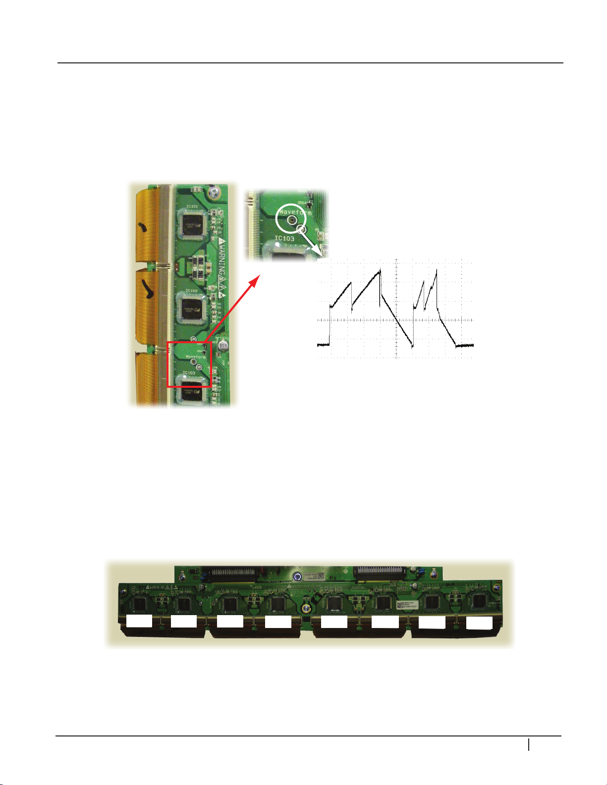
Y-DRIVE BOARD
Y-Drive board works as a path supplying the Sustain and Reset waveforms which are made
in the Y-Sustain board and sent to the panel through scan driver IC’s. The Y-Drive boards
supply a waveform which selects the horizontal electrodes sequentially. The 42PG20 uses
8 driver ICs on 1 Y-Drive board.
4
2
P
G
2
5 Volts and Logic Signals from Y-Sus board are supplied to the Drive board on connector
P200. Logic Signals are from P100. The 5V supply is underneath the board.
0
PDP Training - Fall 2008 37
Page 40
4
Gently Pry Up Here
Locking Tab in Upright Position
Before removing, lift
up slightly to be sure
ribbon cable is released.
2
P
G
CIRCUIT DESCRIPTIONS
REMOvING RIbbON CAblES
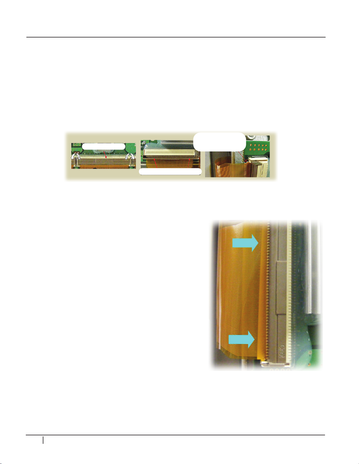
To remove the Ribbon Cable from the connector, first carefully lift the Locking Tab from
the back and tilt it forward (lift from under the tab as shown in Fig 1). The locking tab
must be standing straight up as shown in Fig 2. Lift up the entire Ribbon Cable gently to
release the Tabs on each end. (See Fig 2) Gently slide the Ribbon Cable free from the
connector. To reinstall the Ribbon Cable, carefully slide it back into the slot see ( Fig 3),
be sure the Tab is seated securely and press the Locking Tab back to the locked position
see (Fig 2 then Fig 1).
2
0
Fig 1
INCORRECT INSTAll
In the image to the right, the ribbon cable is improperly
seated into the connector. You can tell by observing
the linearity. The Locking Tab will offer a greater
resistance to closing in this case. Note that the cable
is crooked. In this case the tab on the ribbon cable was
improperly seated at the bottom. This can cause bars,
lines, intermittent lines abnormalities in the picture.
Remove the ribbon cable and re-seat it correctly.
Fig 2
Fig 3
38 PDP Training - Fall 2008
Page 41
CIRCUIT DESCRIPTIONS
Anywhere
BACK SIDE OF Y-DRIVE
RED LEAD ON
A
RED LEAD ON “B”
READING 0.73 V
BLACK LEAD ON
A
BLACK LEAD ON “B”
READING “OPEN”
A
B
FORWARD
REVERSE
RED LEAD ON
BUFFER IC
BLACK LEAD ON “ANY”
OUTPUT LUG.
READING 0.73 V
OUTPUT LUGS
BLACK LEAD ON
BUFFER IC
RED LEAD ON “ANY”
OUTPUT LUG.
READING “OPEN”
Indicated by Red outline
BACK SIDE OF Y-DRIVE PWB
Indicated by Red outline
Y-DRIvE bUFFER TROUblEShOOTING
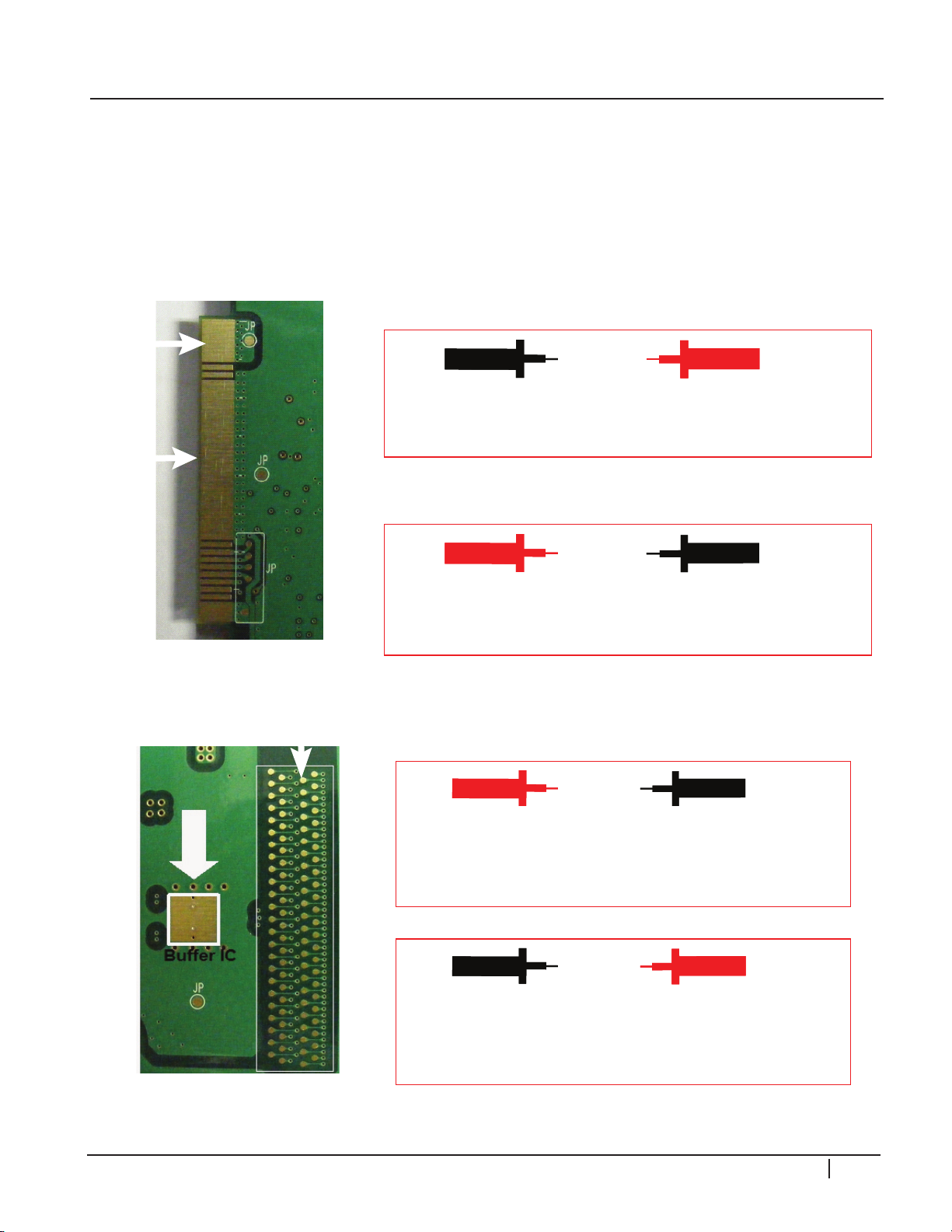
Using the “Diode Test” on the DVM, check the pins for shorts or abnormal loads. You
can check all 8 buffer ICs using this procedure. Using the “Diode Test” on a digital volt
meter, check the pins for shorts or abnormal loads. Any of the output lugs can be tested.
Look for shorts indicating a defective Buffer IC.
4
2
+
-
+
G
2
P
0
+
-
-
-
+
PDP Training - Fall 2008 39
Page 42
4
OS2
P200
TOP (Front View)
OS2
LE
CLK
DATA
52.3V
0V
-87.9V
-87.9V
0V
0V
-83V
-88V
-87.9V
-83V
-90.8V
-87.9V
-85.2V
2
P
G
2
0
CIRCUIT DESCRIPTIONS
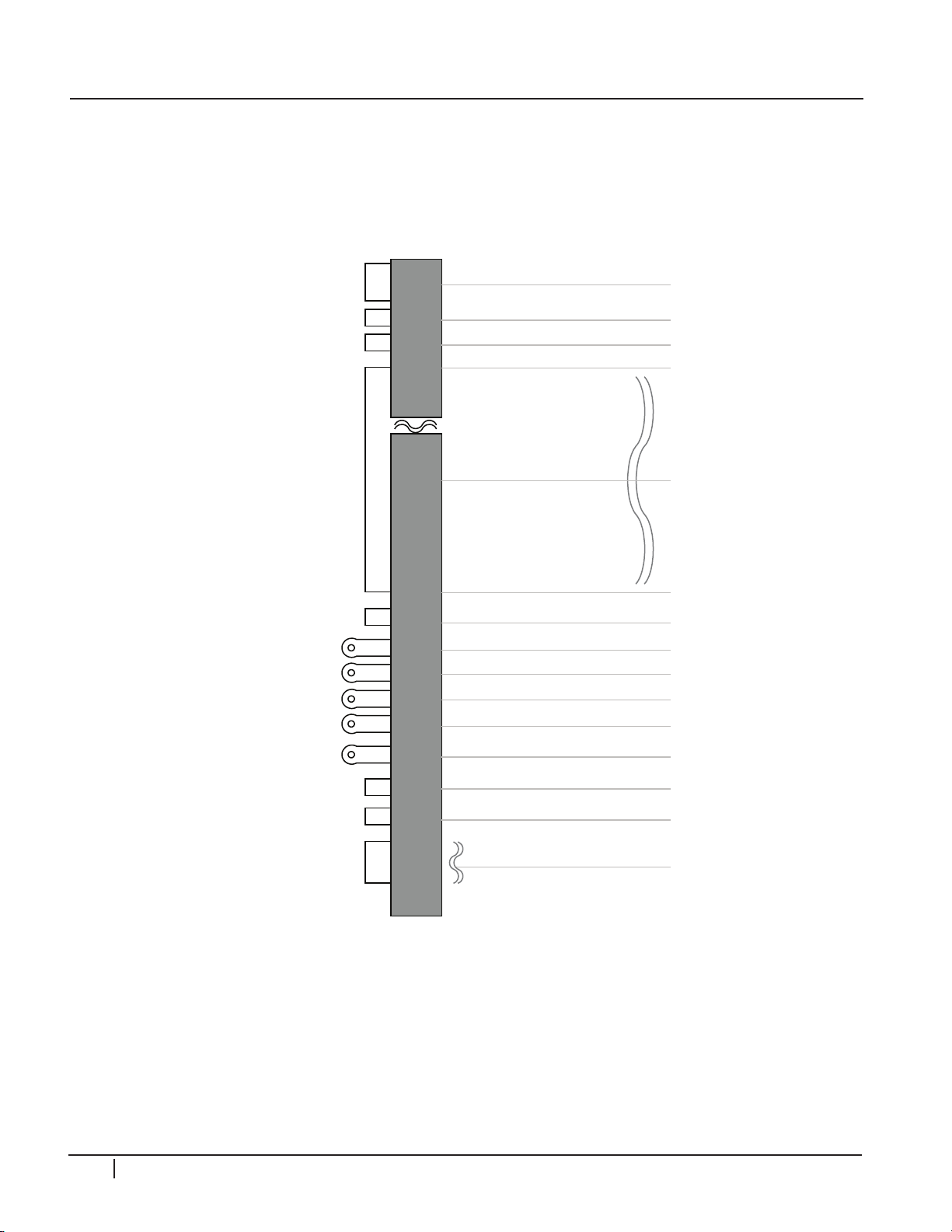
P200 ON ThE Y-DRIvE
Voltages taken with unit running and snow as a picture.
40 PDP Training - Fall 2008
Page 43
CIRCUIT DESCRIPTIONS
FS201
5V
Z-Bias ADJ VR905
P101
Logic Signals
From Control
Z-Bias TP R496
P801
Z-Drive to
Z output
P201
Vs & Va
From SMPS
FS701 (Va)
10A
P202
5V/Va to Left X
FS202 (Vs)
4A 250V
Y-Sus
Output
ICs
Y-Sus
Section
Z-Sus
Section
+
-
Z-bIAS ADJUSTMENT
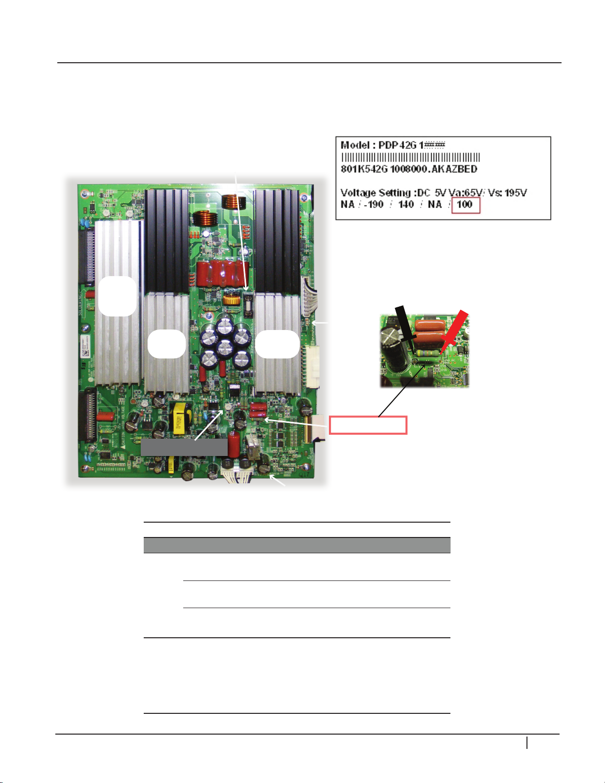
The Z-Sus Drive section is now located on the Y-Sus board. Set should run for 15 minutes
in “Heat Run” mode prior to any adjustments. Set screen to white wash mode or 100IRE
White input. Adjust VZ (Z-Bias) to 100V (+/- 1V).
Read the Label on the back of the
upper left hand side of the panel.
Adjust R946 to that voltage.
4
2
P
G
2
Board Voltage Description
Y-Sus
Z-Sus Z-Bias
VS
VA
M5V VCC
Z-Sus Input Voltages
VS is input at P3 pins 1 and 2 and supplied to the
driver IC circuit.
VA inputs at P3 pins 6 and 7 and supplied to the
driver IC circuit.
5V in input P3 pins 9 and 10. It is used to Bias
the circuits on the Z_ SUS board.
Z Bias Voltage is used to Bias the output circuits
driving the Sustain and Erase
Pulses, removing previous images from the
PDP. Z-bias is measured from the
Vzb TP on the Z -SUS board and adjusted by
VZB Adj.
0
PDP Training - Fall 2008 41
Page 44
4
Z-Drive Wavefrorm
2 ms/Div
100 us/Div
(Vzb) Z-Bias VR905
Vzb Voltage
100V ±1V
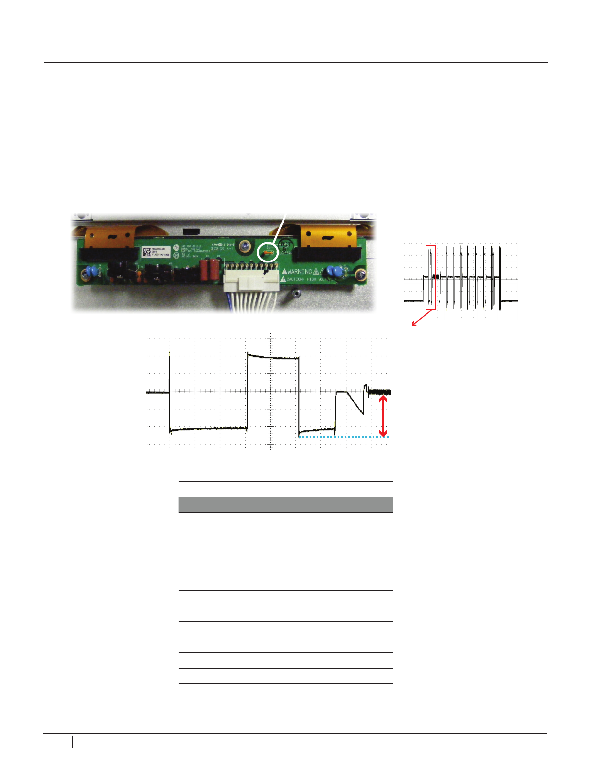
Probe Test Point
2
P
G
2
CIRCUIT DESCRIPTIONS
Z-SUS BOARD
Provides the SUSTAIN PULSE and ERASE PULSE for generating SUSTAIN discharge in
the panel by receiving Drive signals from the Y/Z-Sus board. This waveform is supplied
to the panel through FPC (Flexible Printed Circuit (Z). Z-Bias is a “DC” adjustment. The
effects of this adjustment can be observed on the scope looking at the Z-Sus output.
This Waveform is just for reference to observe the effects of Zbz adjustment. Note: The
Vzb Adjustment is a DC level adjustment.
0
“Y-Sus” P801 to “Z-Drive” P1
Pin Label Standby Run Diode Mode
1 +Vs 0V *194V Open
2 Gnd Gnd Gnd Gnd
3 ZSUS 0V 70.46V Open
4 Gnd Gnd Gnd Gnd
5 ZSUS 0V 70.46V Open
6 Gnd Gnd Gnd Gnd
7 ZSUS 0V 70.46V Open
8 Gnd Gnd Gnd Gnd
9 ZSUS 0V 70.46V Open
10 Gnd Gnd Gnd Gnd
11 ZSUS 0V 70.46V Open
42 PDP Training - Fall 2008
Page 45
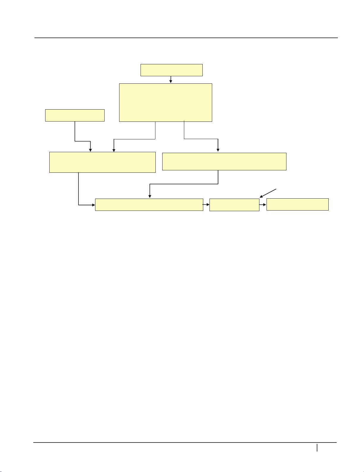
Z-SUS blOCk DIAGRAM
Circuits generate erase,
sustain waveforms
Generates Z Bias 100V
Distributes Logic Signals
Distributes 5V VCC, VA, VS
FET Makes Drive waveform
Display Panel
Via FPC
(flexible printed circuit )
Control Board
Z-SUS Section of the Y-
SUS PWB Receives
VS M5V
Y-SUS Board
Z-SUS FETs
Via P801 to P1
NO IPMs
Z-SUS PWB
CIRCUIT DESCRIPTIONS
4
2
P
G
2
0
PDP Training - Fall 2008 43
Page 46
4
IC211
P160
To Y/Z-Sus
P162
To X-Drive Right
Temperature
LEDs
P121
P131
Download
Connection
P164
n/c
IC121
Auto Gen
Test Pattern
IC201
MCM
IC212
IC213
IC122
IC133
IC171
Pin1 = 3.29V
Pin2 = 1.20V
Pin3 = 0V
IC171
IC101
VS_DA
3V ~3.3V
P161
To X-Drive Left
Crystal
2
P
G
CIRCUIT DESCRIPTIONS
CONTROL BOARD
2
0
Control board Inputs
Board Input
Main LVDS
Y-Sus 5V VCC
1.8V
3.3V
Developed
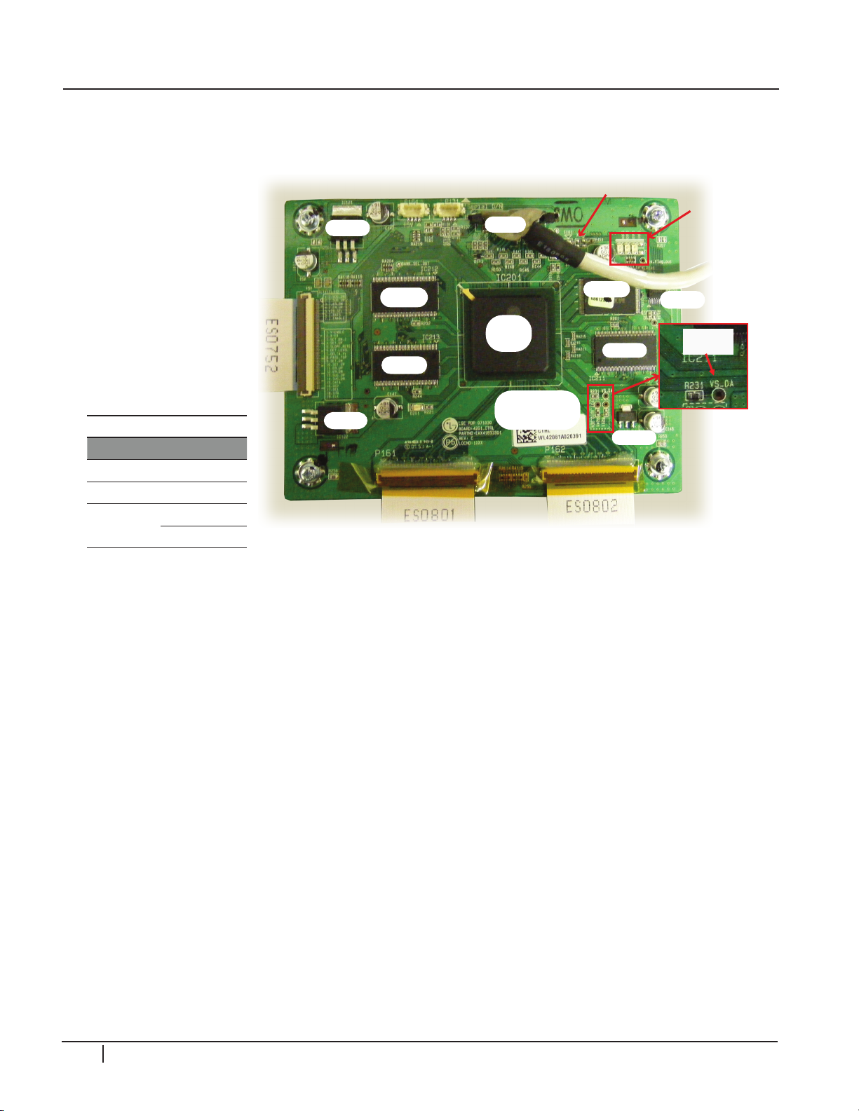
CONTROl bOARD TEST
For a quick board test. (All board connectors Disconnected). Jump 5V from Power Supply
to IC121 Pin 1. If the Temp LED lights, Pretty much guaranteed, board is OK. When the
Television has a problem related to; Shutdown caused by Main board No Picture. This
can be checked by disconnecting the Main board from all connectors. Apply AC power.
Since P813 is not connected, the set will come on. Short the two pins on the Auto Test
Pattern lands.
44 PDP Training - Fall 2008
Page 47
CIRCUIT DESCRIPTIONS
P121
Auto Gen
P161
P162
P164 P131
TEMP LEDS
IC121
X101
Download
Connector
IC212
IC213
IC201
IC211
IC101 IC133
D15 D16 D17
Crystal TP
50Mhz
VS_DA
Control PWB Check
3V ~ 3.3V
RGB Logic
Signals to
Center X PWB
RGB Logic
Signals to
Center R PWB
Auto Test Pattern Generator
Short Lands together
IC171
Pin 1 – 3.29V
Pin 2 – 1.20V
Pin 3 – 0V
IC122
IC122
Pin 1 – 4.75V
Pin 2 – 3.3V
Pin 3 – 0V
P160
Logic Signals to
Y-SUS PWB
Control Board
IC121
Pin 1 – 4.75V
Pin 2 – 3.3V
Pin 3 – 0V
IC171
LVDS
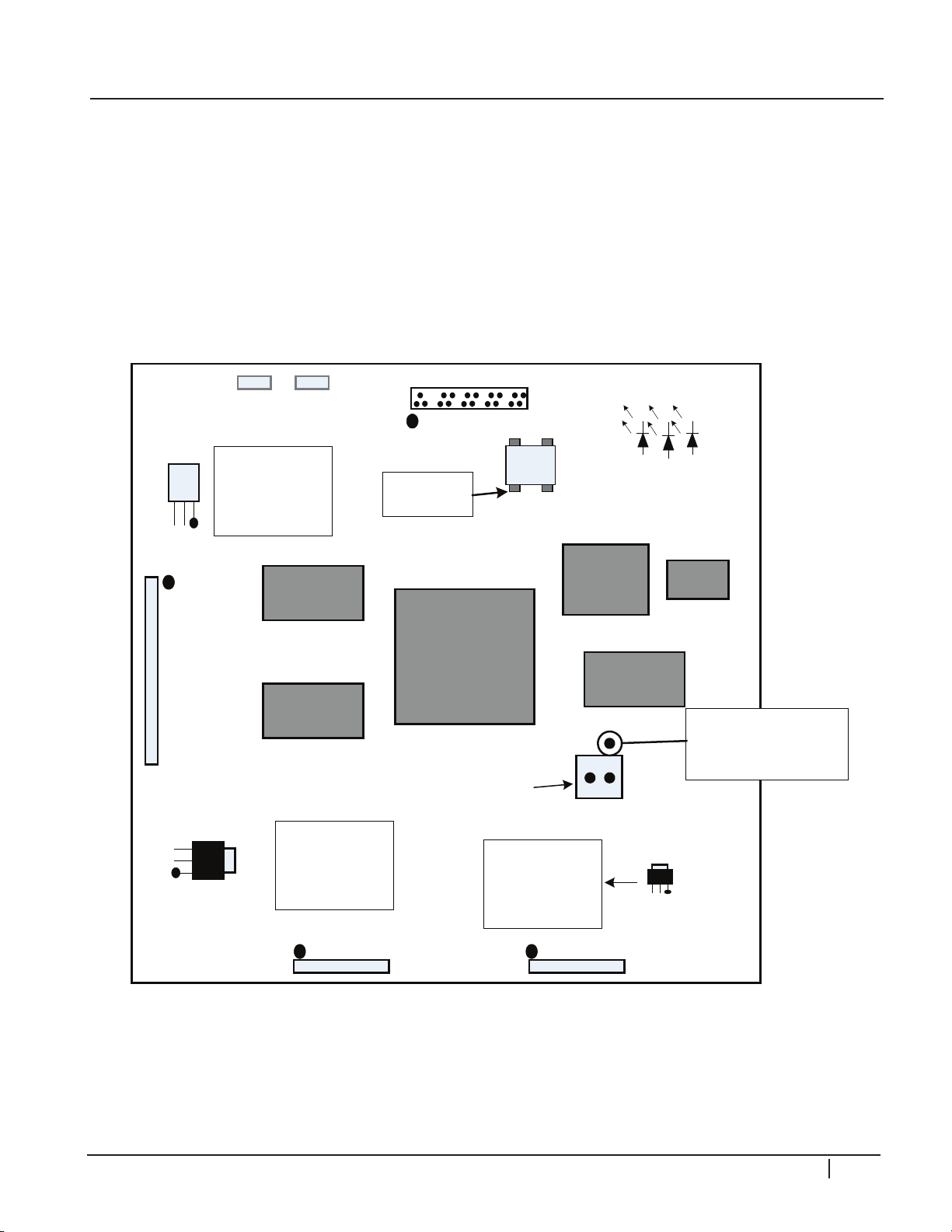
If there is a picture of cycling colors, the Y-Sus, Y-Drive, Z-Sus, Power Supply, Control
boards and Panel are all OK. Same test to tell if No Video is caused by the Main board.
Quick observation Of Temperature LEDs will tell if the Control board is running. With the
unit on. If none of D15, 16, 17 are illuminated. Check supplies to the board. If they are
present replace the Control board.
4
2
P
G
2
0
PDP Training - Fall 2008 45
Page 48
4
50 Mhz
Example of Normal Signals measured at 200mv/cm at 5µs/cm.
Menu OnMenu O
1
3
5
7
9
11
13
15
17
19
21
2
4
6
8
10
12
14
16
18
20
22
-
indicates signal pins.
P302 on Main Board
Locking Tabs
Press In
Press In
2
P
CIRCUIT DESCRIPTIONS
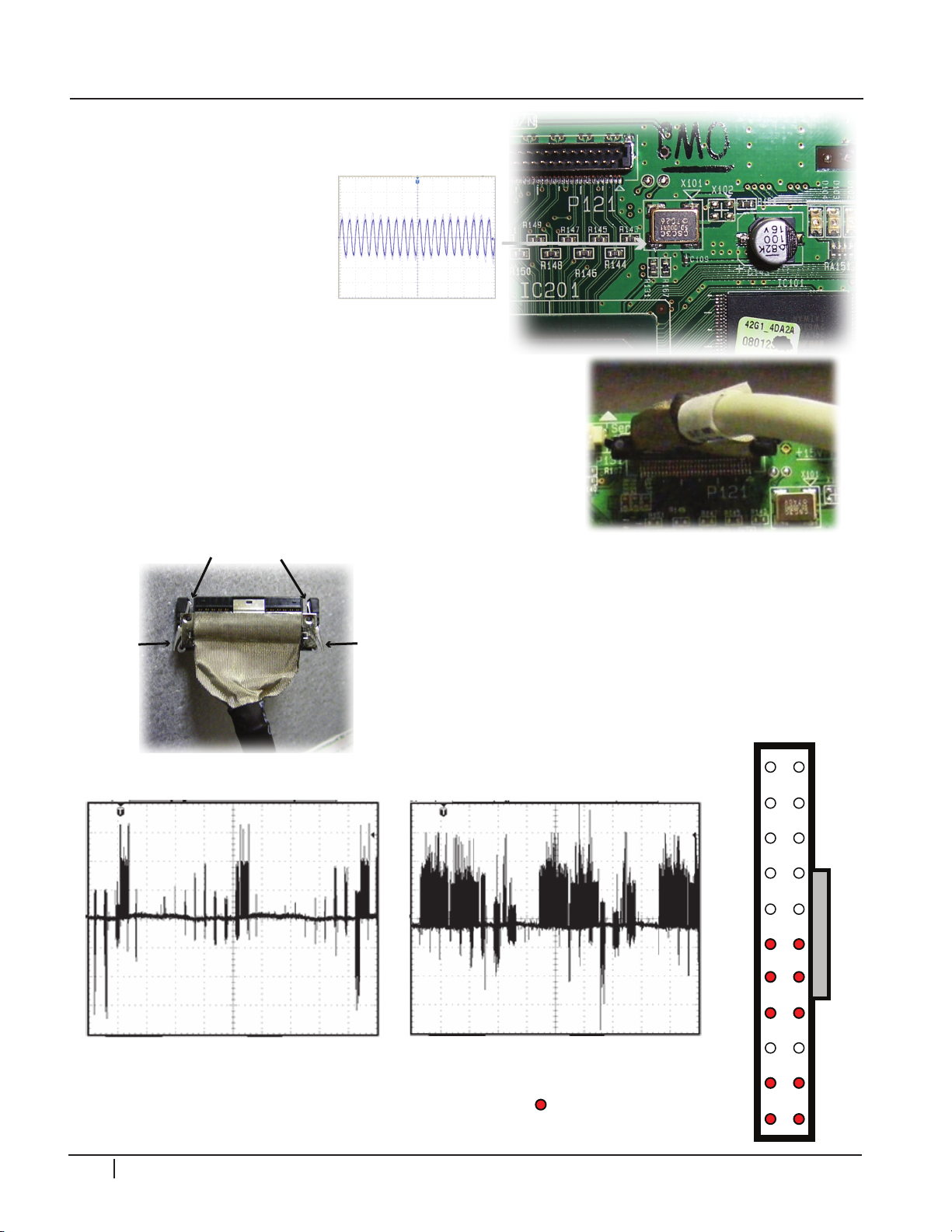
CRYSTAl ClOCk
Ch eck t he ou tpu t o f
the Oscillator package.
The freq uency of the
sine wave is 50 MHZ.
Missing this clock signal
can halt operation of the
unit.
G
2
0
lvDS CAblE
Video Signals from the Main board to the Control board
are referred to as Low Voltage Differential Signals or LVDS.
Their presence can be confirmed with the Oscilloscope by
monitoring the LVDS signals with no input signal selected
while pressing the
Menu Button on and off with the remote control
or keypad. Loss of these signals would confirm the
failure is on the Main board.
P121 on the Control board shown. Press the two
outside tabs inward to release.
46 PDP Training - Fall 2008
Page 49
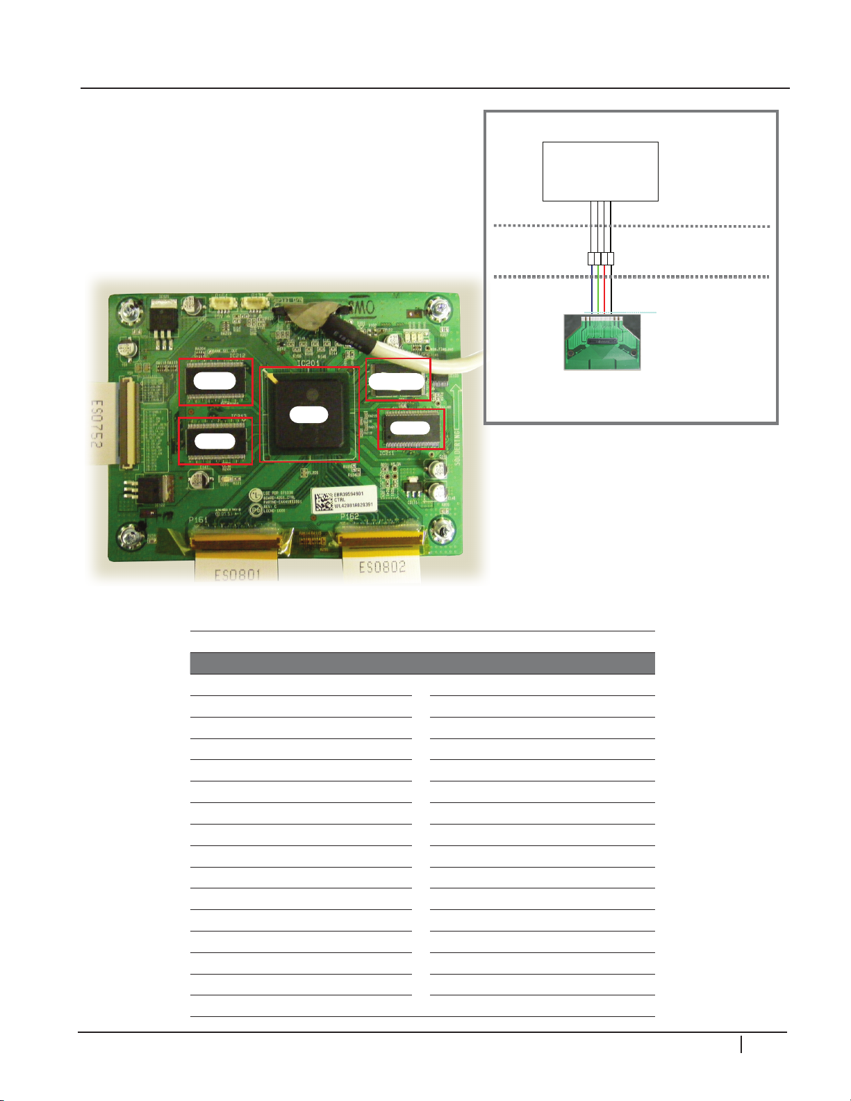
CONTROl bOARD SIGNAl blOCk
DRAM
MCM
DRAM
DRAM
EEPROM
MCM
16 line
Resistor Array
192 Lines output Total
IC201
2 Buffer
Outputs
per TCP
CONTROL PWB
X-DRIVE PWB
PANEL
96 Lines per Buffer
The Control board supplies Video Signals to
the TCP (Tape Carrier Package) ICs. If there is a
bar defect on the screen, it could be a Control
board problem. This Picture shows Signal Flow
Distribution to help determine the failure
depending on where the it shows on the screen.
CIRCUIT DESCRIPTIONS
4
2
P
G
2
P121 “Control” to P302 “Main”
Pin Stby Run Diode Check Pin Stby Run Diode Check
1 Gnd Gnd Gnd 2 0V 0V 1V
3 0V 0V 1V 4 0V 1.26V 1V
5 0V 1.19V 1V 6 0V 0V Gnd
7 0V 1.26V 1V 8 0V 1.19V 1V
9 0V 0V 1V 10 0V 0V 1V
11 0V 1.15V 1V 12 0V 1.26V 1V
13 Gnd Gnd Gnd 14 0V 0V Gnd
15 0V 0V 1V 16 0V 0V 1V
17 0V 0V 1V 18 0V 0V 1V
19 Gnd Gnd Gnd 20 0V 0.21V 1V
21 0V 0V 1V 22 0.89V 0.56V 2.5V
23 0V 5.29V 2.4V 24 0V 1.26V 1V
25 0V 1.2V 1V 26 Gnd Gnd Gnd
27 0V 3.29V 1.3V 28 0.89V 3.29V Open
29 0.89V 3.29V Open 30 0V 0V Open
31 Gnd Gnd Gnd
0
PDP Training - Fall 2008 47
Page 50
4
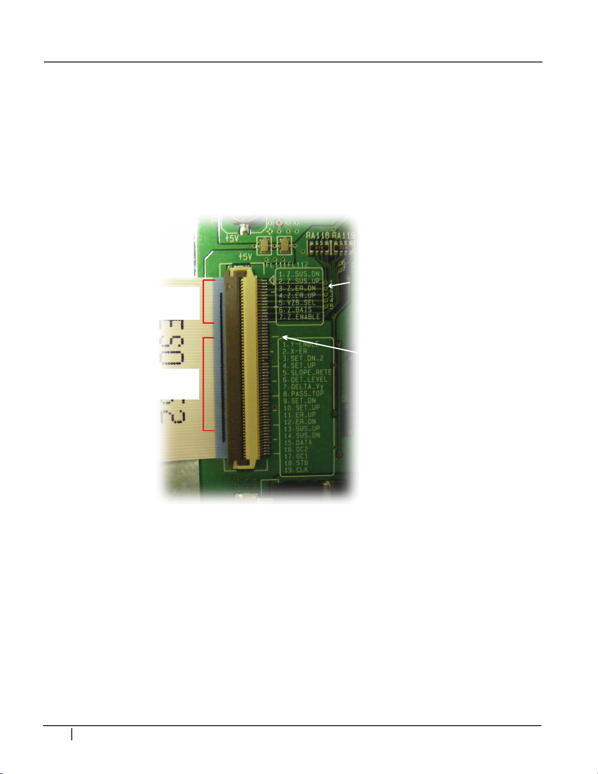
14 Pins Related
to Z-Sus
39 Pins related
to Y-Sus
This labeling does not refer to
P160 pin ID. This too has
ground between each pin.
These are responsible for Z
Drive signals.
Pins 17, 18, 19, 20 and 21
Deliver +5V to the Control
board from the Y-Sus. Easy to
check using 20th hash mark.
P160
20th Hash Mark
2
P
G
2
CIRCUIT DESCRIPTIONS
CONTROl TO Y-SUS
P160 is show below. These pins are very close together, so use caution when taking voltage
measurements. This connector is a little confusing in its labeling. It is actually a 60 pin
connector. This shows the Pin Labeling that is shown on the silk screening. Remember,
this connector has many more pins than the labels indicate. Actual Pin 1 (ground) 2
(Z-Sus-DN) 3 (ground) 4 (Z-Sus-UP) 5 (ground), etc. In other words, there is a ground
between each pin except the +5V area.
0
48 PDP Training - Fall 2008
Page 51
CIRCUIT DESCRIPTIONS
4
2
P
G
2
P101 “Y-Sus” to P160 “Control”
0
2 CLK 0V 3.2V 2.87V 22 Set_DN2 0V 0.2V 2.87V 42 5V OV 4.75V 0.76V / (1.7K)
1 Gnd Gnd Gnd Gnd 21 Gnd Gnd Gnd Gnd 41 5V OV 4.75V 0.76V / (1.7K)
Pin Label STBY Run Diode Mode Pin Label STBY Run Diode Mode Pin Label STBY Run Diode Mode
5 Gnd Gnd Gnd Gnd 25 Gnd Gnd Gnd Gnd 45 n/c n/c n/c n/c
4 STB 0V 0.76V 2.87V 24 PASS_TOP 0V 0.2V 2.87V 44 5V OV 4.75V 0.76V / (1.7K)
3 Gnd Gnd Gnd Gnd 23 Gnd Gnd Gnd Gnd 43 5V OV 4.75V 0.76V / (1.7K)
6 OSC1 0V 0V 2.87V 26 DELTA_Vy 0V 0.16V 2.87V 46 n/c n/c n/c n/c
7 Gnd Gnd Gnd Gnd 27 Gnd Gnd Gnd Gnd 47 Z-ENABLE 0V 0V 1.25V
8 OSC2 0V 3V 2.87V 28 DET_LEVEL 0V 0V 2.87V 48 Gnd Gnd Gnd Gnd
9 Gnd Gnd Gnd Gnd 29 Gnd Gnd Gnd Gnd 49 Z-BIAS 0V 1.71V 1.1V
10 D ATA 0V 0.6V 2.87V 30 SLOPE_RETE 0V 0V 2.87V 50 Gnd Gnd Gnd Gnd
11 Gnd Gnd Gnd Gnd 31 Gnd Gnd Gnd Gnd 51 VZB-SEL 0V 0V 1.1V
12 SUS_DN 0V 0V 2.87V 32 SET_UP 0V 1.9V 2.87V 52 Gnd Gnd Gnd Gnd
13 Gnd Gnd Gnd Gnd 33 Gnd Gnd Gnd Gnd 53 Z-ER_UP 0V 1.25V 1.1V
14 SUS_UP 0V 2V 2.87V 34 Set_DN_2 0V 1.4V 2.87V 54 Gnd Gnd Gnd Gnd
15 Gnd Gnd Gnd Gnd 35 Gnd Gnd Gnd Gnd 55 Z-ER_DN 0V 1.35V 1.1V
20 SET_UP 0V 0.26V 2.87V 40 5V OV 4.75V 0.76V / (1.7K) 60 Gnd Gnd Gnd Gnd
19 Gnd Gnd Gnd Gnd 39 n/c n/c n/c n/c 59 Z-Sus_DN 0V 1.15V 1.1V
18 ER_UP 0V 2V 2.87V 38 Y-Enable 0V 0.6V 2.87V 58 Gnd Gnd Gnd Gnd
17 Gnd Gnd Gnd Gnd 37 Gnd Gnd Gnd Gnd 57 Z-Sus_UP 0V 0.35V 1.1V
16 ER_DN 0V 1.2V 2.87V 36 X_ER 0V 2.9V 2.87V 56 Gnd Gnd Gnd Gnd
PDP Training - Fall 2008 49
Page 52
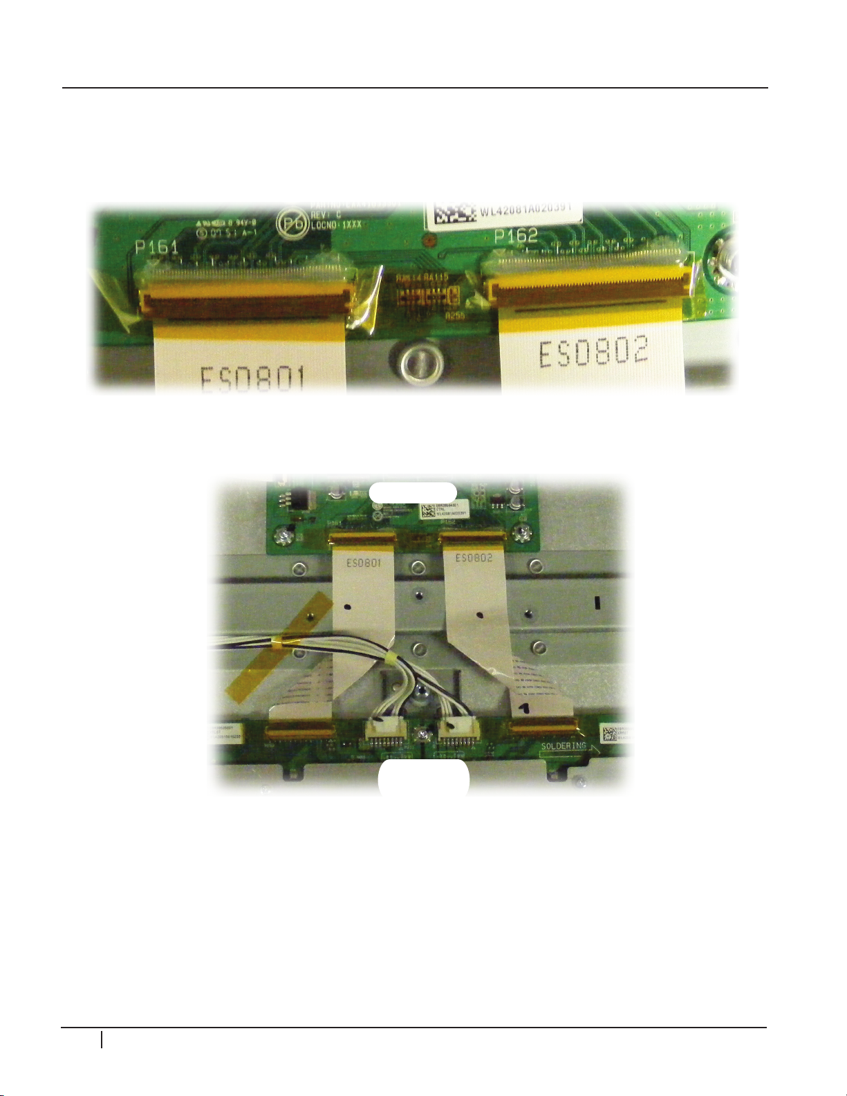
4
Signal Cable
Power Cables
(Va, 15V)
2
P
G
CIRCUIT DESCRIPTIONS
CONTROl TO X-DRIvE
Connector P161 on the Control board connects to P232 on the left X-Drive. Connector
P162 on the Control board connects to P331 on the right X-Drive. These pins are covered
in silicon, so no measurement can be made.
2
0
CONTROl TO X-bOARD
50 PDP Training - Fall 2008
Page 53
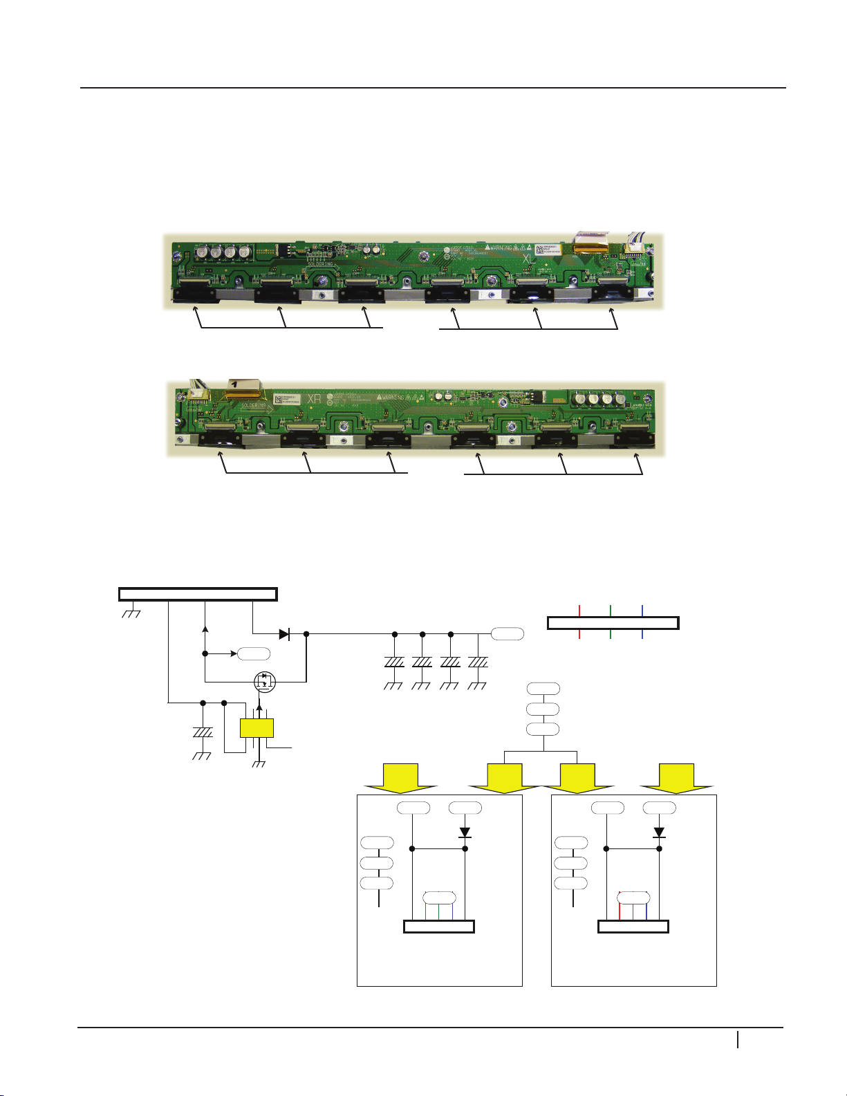
CIRCUIT DESCRIPTIONS
Left X-Board
P311
Right X-Board
P232
TCP ICs
P331
P211
TCP ICs
Va15VGND
+IC+ + +
TCP
X PWB Right
X = 6
EACH PWB HAS THIS SAME CIRCUIT
AFTER Va ARRIVES
VPP
R RGB Signals from the
Control PWB P162
P331
P232
P331
RGB Timing Signals from the Control PWB
From the Y-SUS PWB P210
EACH PWB HAS
THIS SAME CIRCUIT
VPP
Generation
Va
VPP
RGB
VaVPP
P232
L RGB Signals from the
Control PWB P161
Va
VPP
RGB
SUS-Up
1
8
5
4
G
D
S
P211 and P311
TCP
X PWB Left
X = 6
RGB
VaVPP
Va
VPP
RGB
P211 P311
Va
VPP
15V
X-DRIVE BOARDS
Warning: DO NOT attempt to run the set with the heat sinks removed from the TCPs.
After a very short time, these ICs will begin to self destruct due to overheating. TCP IC’s
shown are part of the Ribbon Cable.
4
2
P
G
2
TAPE CARRIER PACkAGE (TCP)
0
PDP Training - Fall 2008 51
Page 54
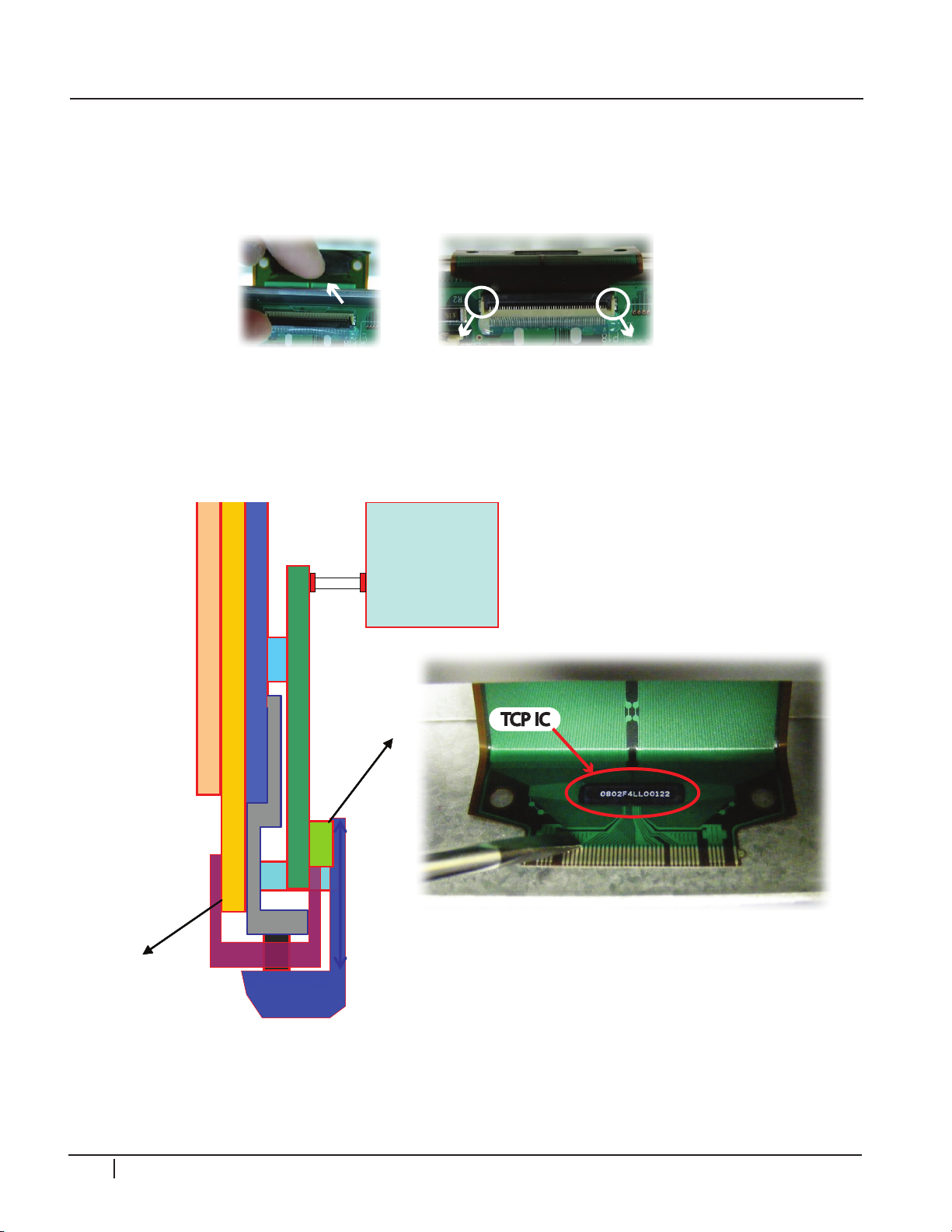
4
TCP
Frame
X_B/D
Front panel Horizontal Address
Rear panel Vertical Address
Frame
X_B/D
Front panel Horizontal Address
Rear panel Vertical Address
Control PWB
2
P
G
2
CIRCUIT DESCRIPTIONS
TCP CONNECTOR REMOvAl
Lift up the lock as shown by arrows. The Lock can be easily broken. It needs to be handled
carefully. Pull TCP apart as shown by arrow. TCP Film can be easily damaged., handle
with care.
TCP ICs supply RGB 16 bit signal to the PDP by connecting the PAD Electrode of the
panel with the X-Board.
0
52 PDP Training - Fall 2008
Page 55
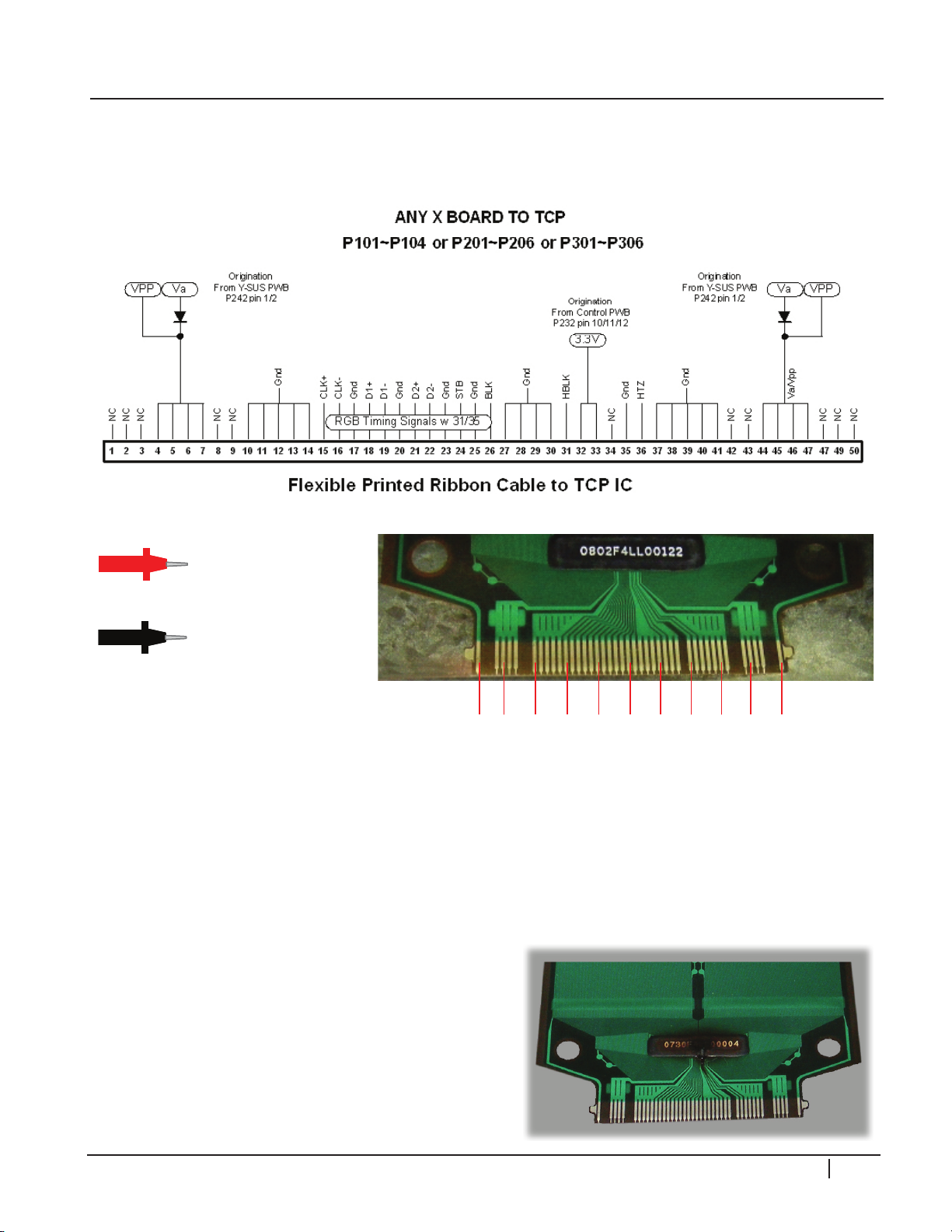
CIRCUIT DESCRIPTIONS
5 10 15 20 25 30 35 40 45 501
On any Gnd
On any Va
4,5,6,7,44,45,46,47
10,11,12,13,14,27,28,2
9,30,37,38,39,40,41
Va VaGnd Gnd
TCP TESTING
Typical Reading 0.65V Opposite reads open. Look for any TCPs being discolored.
Ribbon Damage. Cracks, folds Pinches, scratches, etc.
4
2
P
G
2
+
-
DAMAGED TCP
Warning: DO NOT attempt to run the set with the heat sinks over the TCPs removed.
After a very short time, these ICs will begin to self destruct due to overheating.
A damaged TCP can:
1) Cause the Power Supply to shutdown.
2) Generate abnormal vertical bars.
3) Cause the entire area driven by the TCP
to be “All White”.
0
4) Cause the entire area driven by the TCP
to be “All Black”.
5) Cause a “Single Line” defect.
PDP Training - Fall 2008 53
Page 56
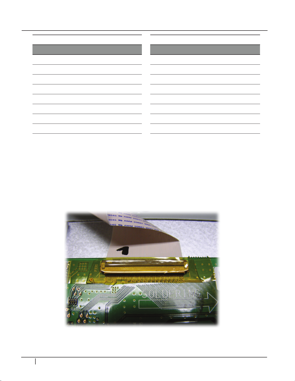
CIRCUIT DESCRIPTIONS
P211 “X-Drive Left” to “Y-Sus” P202 P311 “X-Drive Right” to “Y-Sus” P202
Pin Label Stby Run Diode Check Pin Label Stby Run Diode Check
4
2
P
G
2
0
1 Gnd 0V Gnd Gnd 1 Gnd Gnd Gnd Gnd
2 Gnd 0V Gnd Gnd 2 Gnd Gnd Gnd Gnd
3 15V 0V 15.4V Open 3 15V 0V 15V Open
4 n/c 0V n/a n/a 4 n/c 0V n/a n/a
5 n/c 0V n/a n/a 5 n/c 0V n/a n/a
6 VPP 0V *61.4V Open 6 VPP 0V *61.4V Open
7 VPP 0V *61.4V Open 7 VPP 0V *61.4V Open
8 VA 0V *64.9V Open 8 VA 0V *64.9V Open
P232 & P331 CONNECTORS
Voltage and resistance measurements for the X-Drive board. Voltage and resistance
measurements for these connectors are difficult to read. They are too close together for
safe test. The pins are also protected by a layer of tape to prevent the tab from being
released causing separation from the cable and the connector. Take resistance readings
with the PCB Disconnected.
54 PDP Training - Fall 2008
Page 57
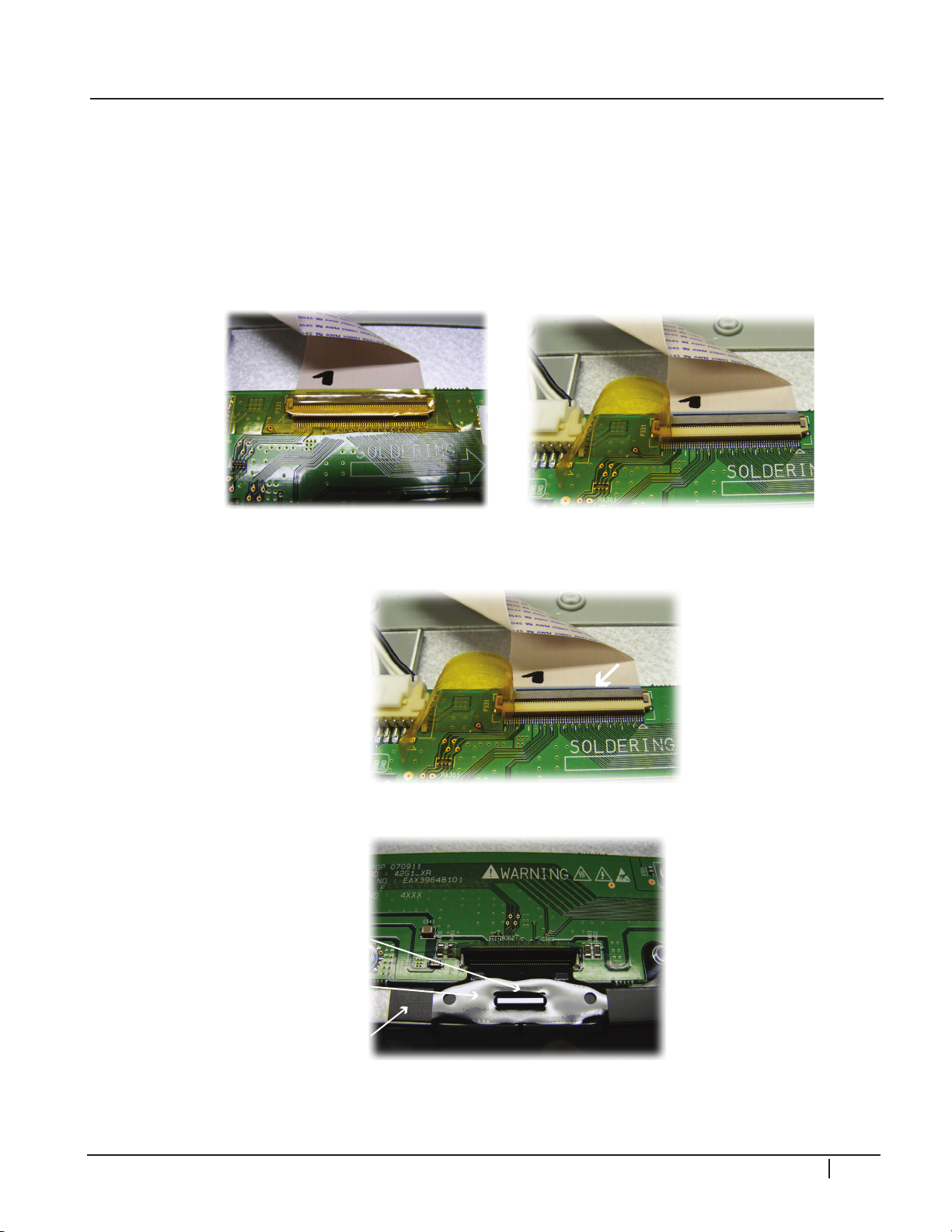
CIRCUIT DESCRIPTIONS
Cushion
TCP
Flexible Ribbon Cable
LEFT AND RIGHT X-DRIVE REMOVAL
After the back cover is removed, the Main board is lifted out of the way, the 15 screws are
removed from the heat sinks covering the TCPs, the X-Drive boards can be removed. Gently
lift the locking mechanism upward on all TCP connectors P201-206 or P301-306.
4
Peel the tape off the P232 or P331 connectors and gently pry the locking mechanism
upward.
Gently pry the locking mechanism upward on all TCP connectors P201-206 or
P301-306.
2
P
G
2
0
Carefully lift the TCP ribbon up and off the cushion and out of the way.
PDP Training - Fall 2008 55
Page 58
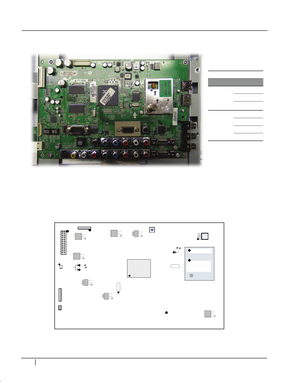
4
P701
P303
JK501
LD703
**LD400
P302
MAIN
PCB
To keys and IR
To Speakers
X400
X100
IC100
Micro
1.5V SBY
12 Meg
25 Meg
Run Only
IC805
IC706
IC709
Grayed Out ICs are
located on Back
IC702
5) .29V
4) 5V
3) 0V
2) 0V
1) 0V
IC709
1) 3.29V
2) 1.26V
3) 0V
IC708
1) 5V
2) 3.31V
3) 0V
IC705
IC705
1) 5V
2) 3.29V
3) 0V
IC706
1) 5V
2) 2.6V
3) 1.37V
IC708
IC501
1) 3.3V
2) 1.8V
3) 0V
IC501
Reset
LVDS
IC805
1) 5V
2) 3.3V
3) 0V*
*
*
*
*
*
*
IC702
IC101
*
IC101
1) 5V
2) 0V
3) 5V
Pin 1
Pin 16
Pin 1
TUNER
TUNER
Pin 16 Video
Pin 14 SIF
Q706
2
P
G
2
CIRCUIT DESCRIPTIONS
MAIN (DIGITAL) BOARD
Main Input Voltages
Board Voltage
5V
SMPS
Main
12V
16V
5V
3.3V
2.5V
1.8V
0
56 PDP Training - Fall 2008
Page 59
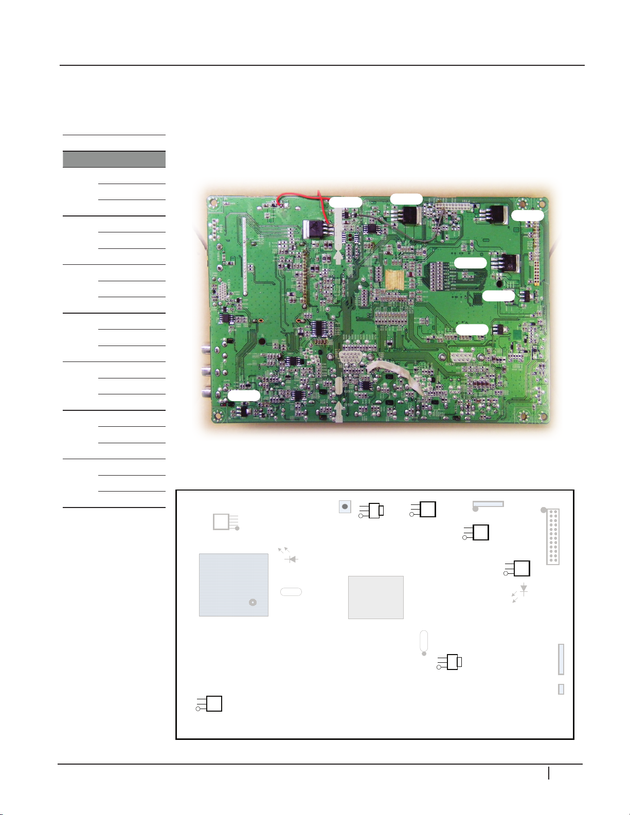
CIRCUIT DESCRIPTIONS
IC705
IC101
IC501
IC708
IC706
IC805
IC709
P701
P303
JK501
LD703
LD400
P302
MAIN PCB
“Back View”
To keys and IR
To Speakers
IC702
TUNER
X400
X100
IC1001
1.5V SBY
12 Meg
25 Meg
Run Only
IC805
IC706
IC709
Grayed Out ICs are
located on Front
IC705
IC101
IC501
Reset
LVDS
*
*
*
*
*
*
*
TUNER
P701
P303
JK501
LD703
**LD400
P302
MAIN
PCB
To keys and IR
To Speakers
X400
X100
IC100
Micro
1.5V SBY
12 Meg
25 Meg
Run Only
IC805
IC706
IC709
Grayed Out ICs are
located on Back
IC702
5) .29V
4) 5V
3) 0V
2) 0V
1) 0V
IC709
1) 3.29V
2) 1.26V
3) 0V
IC708
1) 5V
2) 3.31V
3) 0V
IC705
IC705
1) 5V
2) 3.29V
3) 0V
IC706
1) 5V
2) 2.6V
3) 1.37V
IC708
IC501
1) 3.3V
2) 1.8V
3) 0V
IC501
Reset
LVDS
IC805
1) 5V
2) 3.3V
3) 0V*
*
*
*
*
*
*
IC702
IC101
*
IC101
1) 5V
2) 0V
3) 5V
Pin 1
Pin 16
Pin 1
TUNER
TUNER
Pin 16 Video
Pin 14 SIF
Q706
MAIN bOARD bOTTOM
Be sure to prevent the board from touching the frame while the board is turned over. Use
a piece of cardboard or towel to insulate.
Main ICs
Chip Pin Voltage
1 5V
IC705
IC706
IC708
IC709
IC501
IC805
IC101
2 3.29V
3 0V
1 5V
2 2.6V
3 1.37V
1 5V
2 3.31V
3 0V
1 3.29V
2 1.26V
3 0V
1 3.3V
2 1.8V
3 0V
1 5V
2 3.3V
3 0V
1 5V
2 0V
3 5V
4
2
P
G
2
0
PDP Training - Fall 2008 57
Page 60
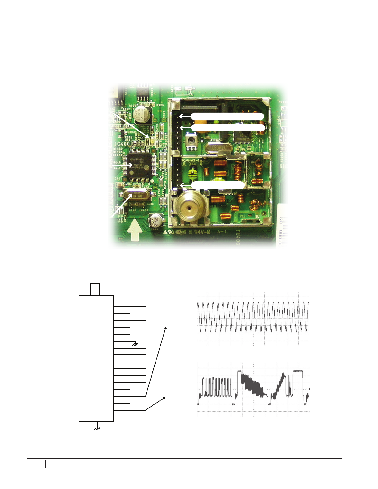
4
Pin 16
Video Signal
Pin 14
SIF Signal
17
16
15
14
13
12
11
10
9
8
7
6
5
4
3
2
1
TDVF-H051F
EBL37676801
NC_1
RF-AGC
+B (5V)
VTU
NC_2
GND
SDA
SCL
AS
DIGITAL_IF1
DIGITAL_IF2
IC_AGC
AUDIO_OUT
SIF
IF_AS
VIDEO_OUT
Shield
Not Used
Not Used
Not Used
Not Used
Not Used
Not Used
Not Used
850mVp/p 20nSec rate
1Vp/p 20uSec rate
X400
Tuner
Controller
Osc.
IC400
Tuner
Controller
LD400
Tuner Osc. Lock
On Unlocked
O Locked
VIF Pin 16 Video Test Point
SIF Pin 14 Audio Test point
Pin 3 Tuner B+ (5V)
2
P
G
2
CIRCUIT DESCRIPTIONS
MAIN bOARD TUNER TEST POINTS
Refer to the image below with the shield off and pins exposed on the tuner.
0
58 PDP Training - Fall 2008
Page 61
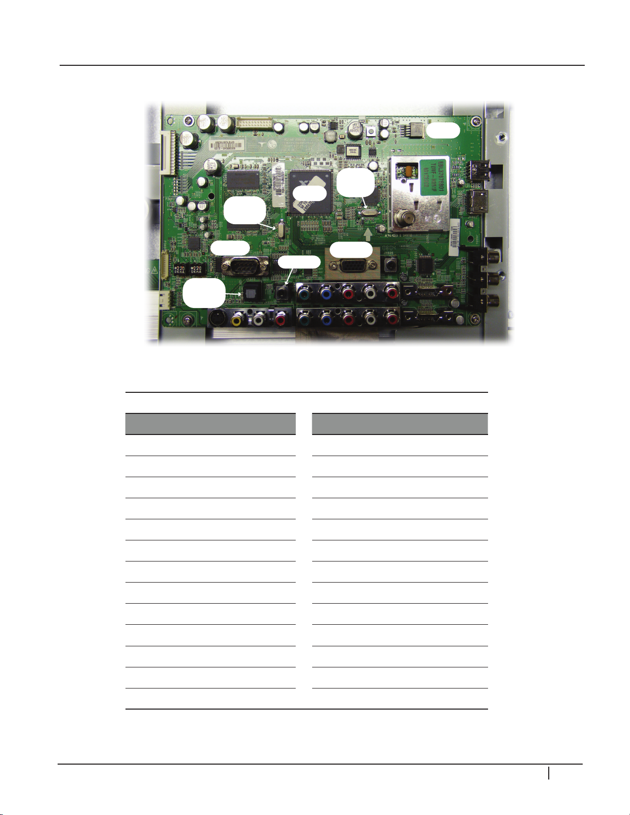
IC702
X100
12 Mhz
P701
To Power Supply
X400
25 Mhz
IC1001
SW100 Reset
USB
RGB/PC
RS-232
JK501
Speaker Out
P303
To Front Controls
P302
LVDS To Control
HDMI Inputs
AV 3
HDMI 3
AudioComponent
Remote
A/V Composite
Optical
Audio
MAIN bOARD CONNECTORS
CIRCUIT DESCRIPTIONS
4
2
P
G
2
P302 “Main” P121 “Control”
Pin Stby Run Diode Check Pin Stby Run Diode Check
1 0V 0V Open 2 0V 0V Open
3 0V 0V Open 4 0V 0V Open
5 Gnd Gnd Gnd 6 Gnd Gnd Gnd
7 Gnd Gnd Gnd 8 Gnd Gnd Gnd
9 0.89V 3.29V 1.97V 10 0.89V 3.29V 1.97V
11 0V 1.25V 1.17V 12 0V 1.21V 1.17V
13 0V 1.25V 1.17V 14 0V 1.21V 1.17V
15 0V 1.27V 1.17V 16 0V 1.21V 1.17V
17 0V 1.22V 1.17V 18 0V 1.25V 1.17V
19 0V 1.24V 1.17V 20 0V 1.21V 1.17V
21 0V 1.24V 0.83V 22 0V 1.18V 1.17V
23 0V 0.58V 1.01V 24 0.93V 3.29V 1.5V
0
25 0V 3.29V Open 26 Gnd Gnd Gnd
PDP Training - Fall 2008 59
Page 62
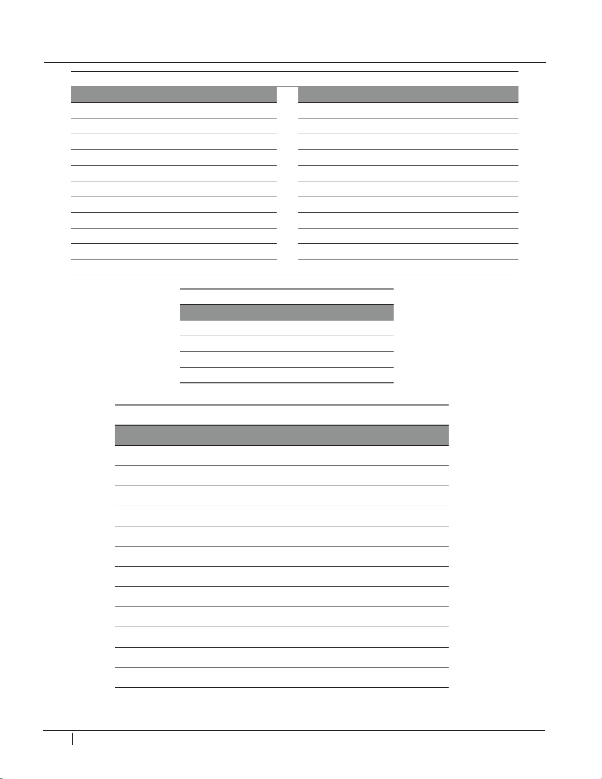
4
2
P
G
CIRCUIT DESCRIPTIONS
P701 “Main” to P813 “SMPS”
Pin Label STBY Run Diode Check Pin Label STBY Run Diode Check
1 15V 0V 16.5V 3.8V 2 15V 0V 16.5V 2.82V
3 Gnd Gnd Gnd Gnd 4 Gnd Gnd Gnd Gnd
5 NC NC NC Open 6 NC NC NC Open
7 Gnd Gnd Gnd Gnd 8 Gnd Gnd Gnd Gnd
9 5V 5V 5V 0.75V 10 5V 5V 5V 0.75V
11 5V 5V 5V 0.75V 12 5V 5V 5V 0.75V
13 Gnd Gnd Gnd Gnd 14 Gnd Gnd Gnd Gnd
15 Gnd Gnd Gnd Gnd 16 Gnd Gnd Gnd Gnd
17 5_V Det .15V 5V 3.25V 18 AC Det 5V 5V Open
19 RL_On 0V 3.73V Open 20 Vs_On 0V 3.2V 1.22V
21 M5V_ 3.27V 3.24V 1.22V 22 AUTO Gnd Gnd Gnd
2
0
CN701 “Main” to “Speakers”
Pin Stby Run Diode Check
1 0V 8V 2.58V
2 0V 8V 2.58V
3 0V 8V 2.58V
4 0V 8V 2.58V
P303 “MAIN” to “Front Keys”
Pin STBY Run Diode Check
1 5V 5V 2.99V
2 Gnd Gnd Gnd
3 0V 3.29V 1.18V
4 Gnd Gnd Gnd
5 0V 3.29V 1.18V
6 Gnd Gnd Gnd
7 5V 5V 0.75V
8 Gnd Gnd Gnd
9 0V 0V 1.12V
10 Gnd Gnd Gnd
11 0V 3.84V 1.03V
12 Gnd Gnd Gnd
Resistance Readings with the board Disconnected. DVM in the Diode mode.
60 PDP Training - Fall 2008
Page 63
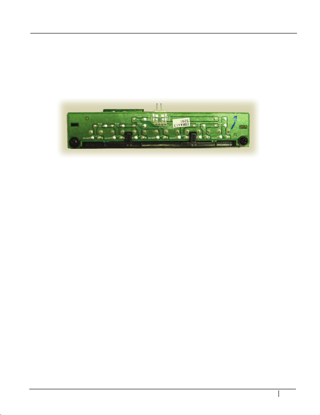
CIRCUIT DESCRIPTIONS
Keypad
Power Switch
POWER SWITCH AND KEYPAD
The Keypad board and Power Switch board are located (as viewed from the rear) in the
lower left hand section. To remove, unplug the connector P101 and remove the 2 screws.
Under each screw there is a black tab. Release these tabs to lift the board upward. Then
remove the connector from the Power Switch board and remove it’s two screws.
4
2
P
G
2
0
PDP Training - Fall 2008 61
Page 64

- 62 -
Page 65
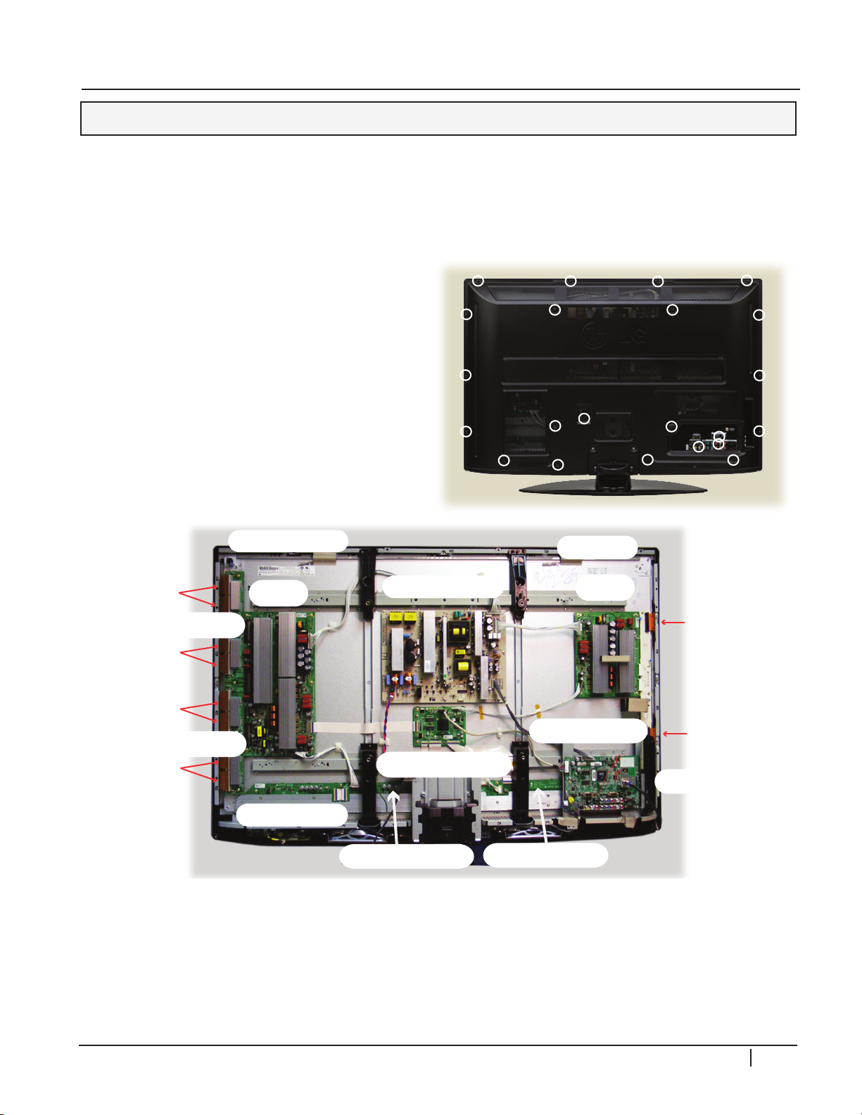
DISASSEMBLY
Y-Sus
Control (Logic)
Upper Y-Drive
Voltage Label
Main (Digital)
Panel ID
Power Supply
Z-Sus
Right X-Board
Left X-Board
Side Inputs
Lower Y-Drive
FPC
FPC
FPC
FPC
FPC
FPC
Center X-Board
DISASSEMBLY 50PG20
INTRODUCTION
This section of the manual will discuss Disassembly of the 50PG20 PDP Direct View
Television. Upon completion of this section the technician will have a better understanding
of the disassembly procedures, the layout of the printed circuit boards and be able
to identify each board. Remember to be
cautious of ESD as many semiconductors are
CMOS and prone to static failure.
BACK COVER REMOVAL
Remove the 22 screws shown. Pay attention
to the size and type of screw as there are
different types. Putting in the improper
screw when reassembling may cause damage.
The stand does not need to be removed.
POWER SUPPLY BOARD REMOVAL
Remove 8 screws securing the Power Supply and disconnect Connectors from Plugs CN101
(AC Input) P801 (Vs, Vs, NC, GND, GND, Va, Va, GND, M5V, M5V), P802 (Vs, Vs, NC,
GND, GND, Va, Va, GND, M5V, M5V), P803 (22 pins).
5
0
P
G
2
0
PDP Training - Fall 2008 63
Page 66
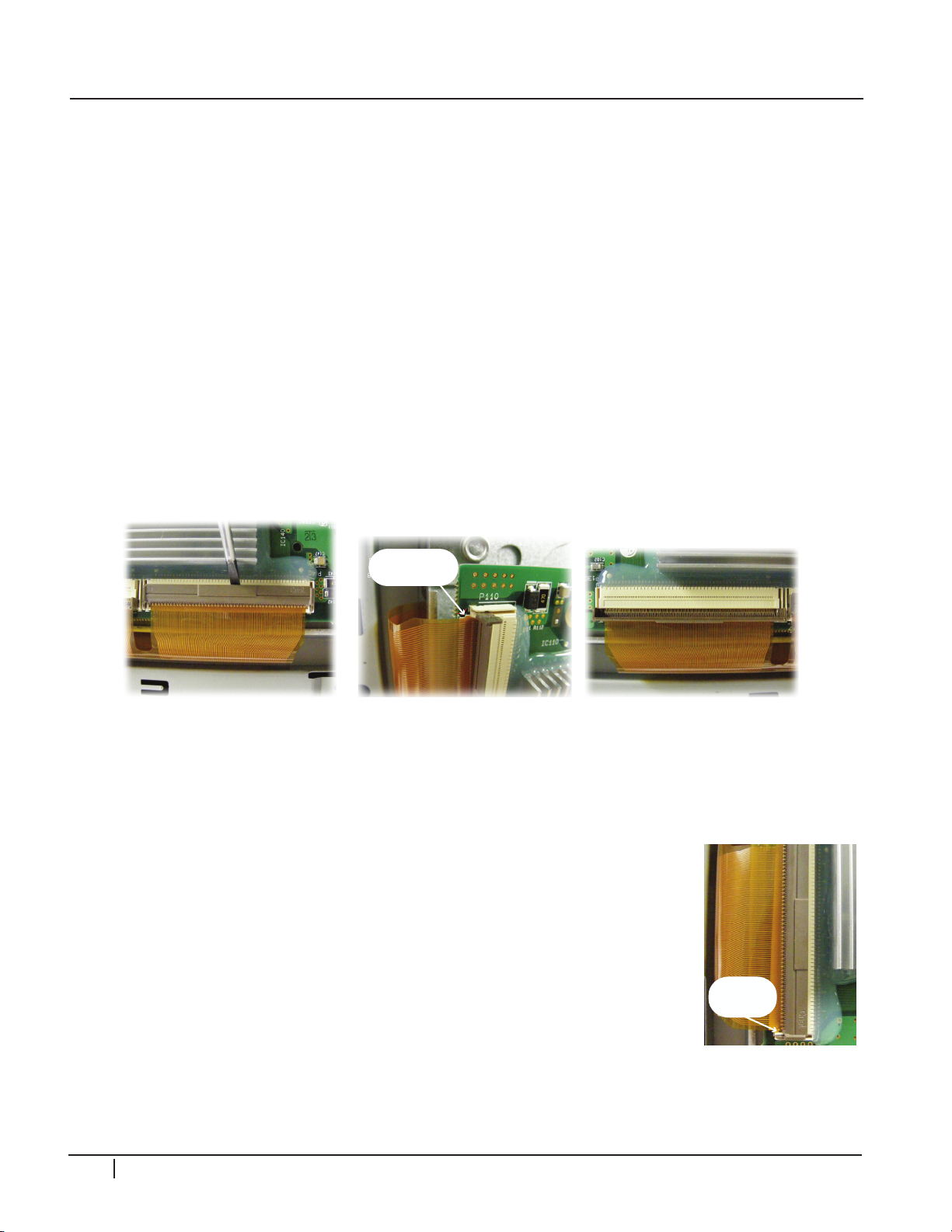
DISASSEMBLY
Tab
Exposed
Figure 1 Figure 2 Figure 3
Be sure tab
is released
After the board is replaced, readjust RV901(VS), RV902 (VA) according to the DC voltage
levels indicated by the voltage label in the upper left corner of the panel.
Y-SUS BOARD REMOVAL
Remove connectors P209, P102 and P210. Then remove the 9 screws holding the Y-Sus
secured. Lift gently and slide board to the right to release from the Upper and Lower
Y-Drive boards.
TOP Y-DRIVE BOARD REMOVAL
Remove the 4 connectors going to the Flexible Ribbon Connectors for the panel. Remove
the 3 screws holding the board in place. Lift the board up to unseat the board from the
stand-off collars and pull the board away from the Y-Sus board connectors.
To remove the Ribbon Cable from the connector first carefully lift the Locking Tab from
the back and tilt it forward (lift from the outside edge as shown in Fig1). Lift up the entire
Ribbon Cable gently to release the tabs on each end. Gently slide the Ribbon Cable free
from the connector.
5
0
P
G
2
0
INCORRECTlY SEATED RIbbON CAblE
The Ribbon Cable shown is improperly seated into the connector. You can tell by
observing the linearity. Note the cable is crooked. In this case the tab on the Ribbon
Cable was improperly seated at the bottom. This can cause bars, lines, and intermittent
lines abnormalities in the picture. Remove the ribbon cable and re-seat
it correctly.
BOTTOM Y-DRIVE BOARD
Remove the 4 connectors going to the Flexible Ribbon Connectors for
the panel. Remove the 3 screws holding the board in place. Lift the
board up to unseat the board from the screw stand-off collars and pull
the board away from the Y-Sus board connectors.
64 PDP Training - Fall 2008
Page 67
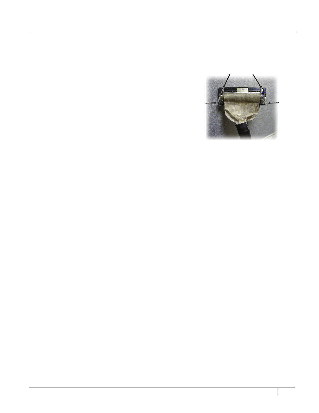
DISASSEMBLY
Locking Tabs
Press In
Press In
Z-SUS BOARD REMOVAL
Remove the P2 and P3 connectors. Remove the 6 Screws Lift the board up slightly and
pull board to the left to disengage the connectors going to the FPC cables interface
boards. When reinstalling board, be sure to check
Va/Vs and then readjust Z-Bias according to the
voltage panel label.
MAIN BOARD REMOVAL
Remove the P302, P303, P701 connectors and the
speaker plug CN701. Remove the 2 Screws holding
the decorative black plastic piece over the input
jacks and remove. Remove the 4 screws holding
the board in place and remove.
NOTE: If the board just needs to be out of the way; Remove the 2 Screws holding the
decorative black plastic piece over the input jacks and remove. Remove the two screws
at the top of the Main board mounting brackets, loosen the tape at the bottom of the
bracket, unplug P701 and CN701 and swing the board up and to the right.
CONTROL BOARD REMOVAL
Remove the following connectors: P111, P163, P162, P161, and P151. Carefully remove the
LVDS Cable P121 from the Control board by pressing the locking tabs together and pulling
straight out. Remove the 4 screws in each corner. Pay attention to the back side. Note:
The rubber type pad is actually a temperature transfer medium. Be sure to remove this
pad from the old board and place the pad back on the new board before installation.
X-BOARD REMOVAL
X-Board removal will require the most disassembly of all the boards. All the brackets
and assemblies marked A-F (Image on next page) will need to be removed including the
stand. Before an X-Board can be removed, the heat sink assembly will also need to be
removed.
Lay the unit face down on non-scratch material. To prevent damage to the LVDS Cable,
carefully remove the LVDS Cable P121 from the Control board by pressing the Locking
Tabs together and pulling straight back to remove the cable (see illustration above).
5
0
P
G
2
0
PDP Training - Fall 2008 65
Page 68
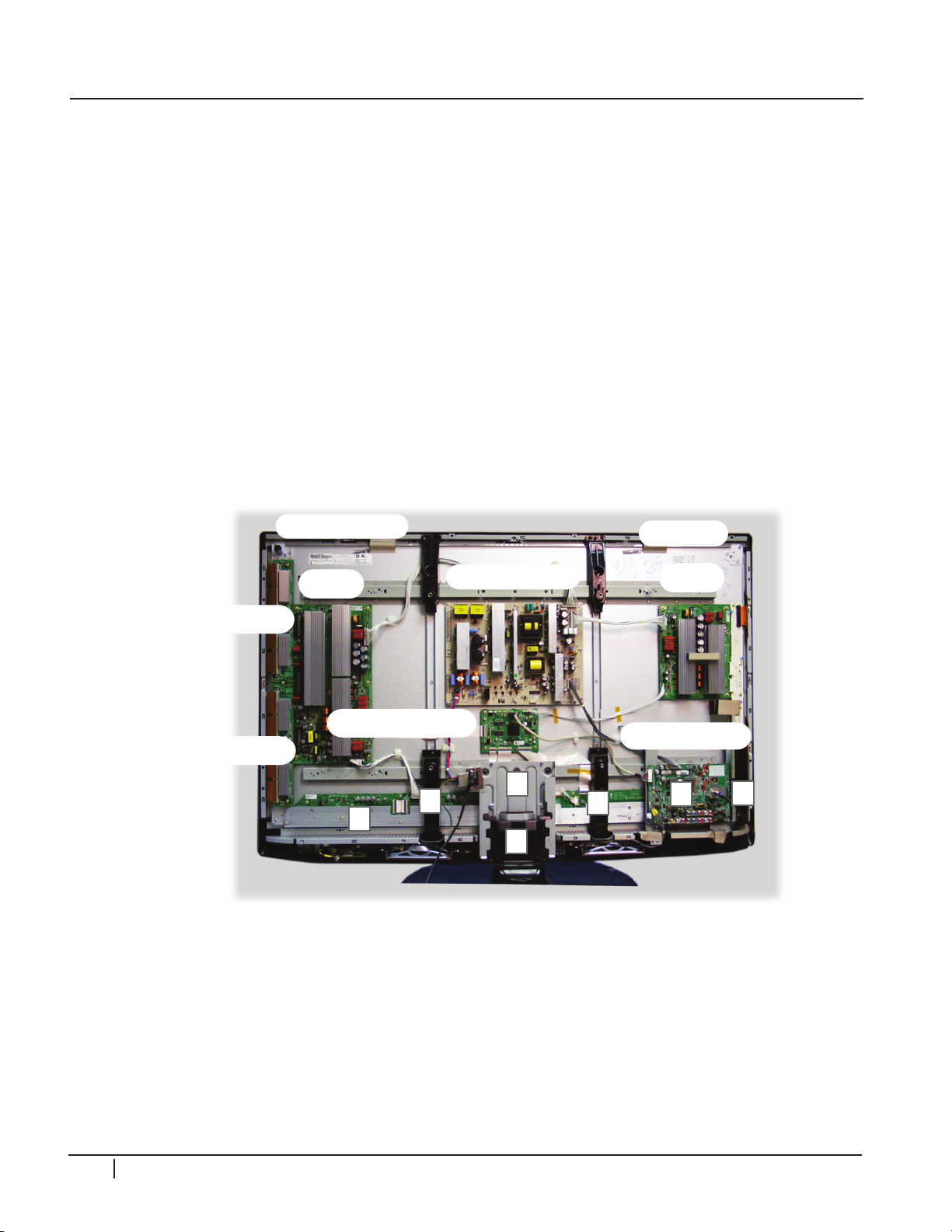
DISASSEMBLY
Y-Sus
Control (Logic)
Upper Y-Drive
Voltage Label
Main (Digital)
Panel ID
Power Supply
Z-Sus
Lower Y-Drive
F
B
E
E
C
D
A
Now remove the following components:
(A) Remove the stand mounting support plastic piece.
(B) Remove the stand metal support bracket, unplug AC ground lug.
(C) Remove the decorative black plastic piece over side inputs.
(D) Remove the two screws at the top of the Main board support bracket. Unplug the
speaker and front Input plugs and swing the board out of the way.
(E) Remove both bottom black support braces. 3 screws each.
(F) Remove the TCP heat sink 9 screws and remove.
Disconnect all connectors going to each board that needs to be removed. Left X-Drive:
P121, P101 through P104. Center X Drive: P242, P241, P232 P211, P201 through P206.
Right X-Drive: P331, P311, P503, P301 through P306. Remove the 4 screws for each
board and remove the board. One of the screws supports two boards. Reassemble in
reverse order. Recheck Va/Vs/VScan/-VY/Z-Drive.
5
0
P
G
2
0
66 PDP Training - Fall 2008
Page 69
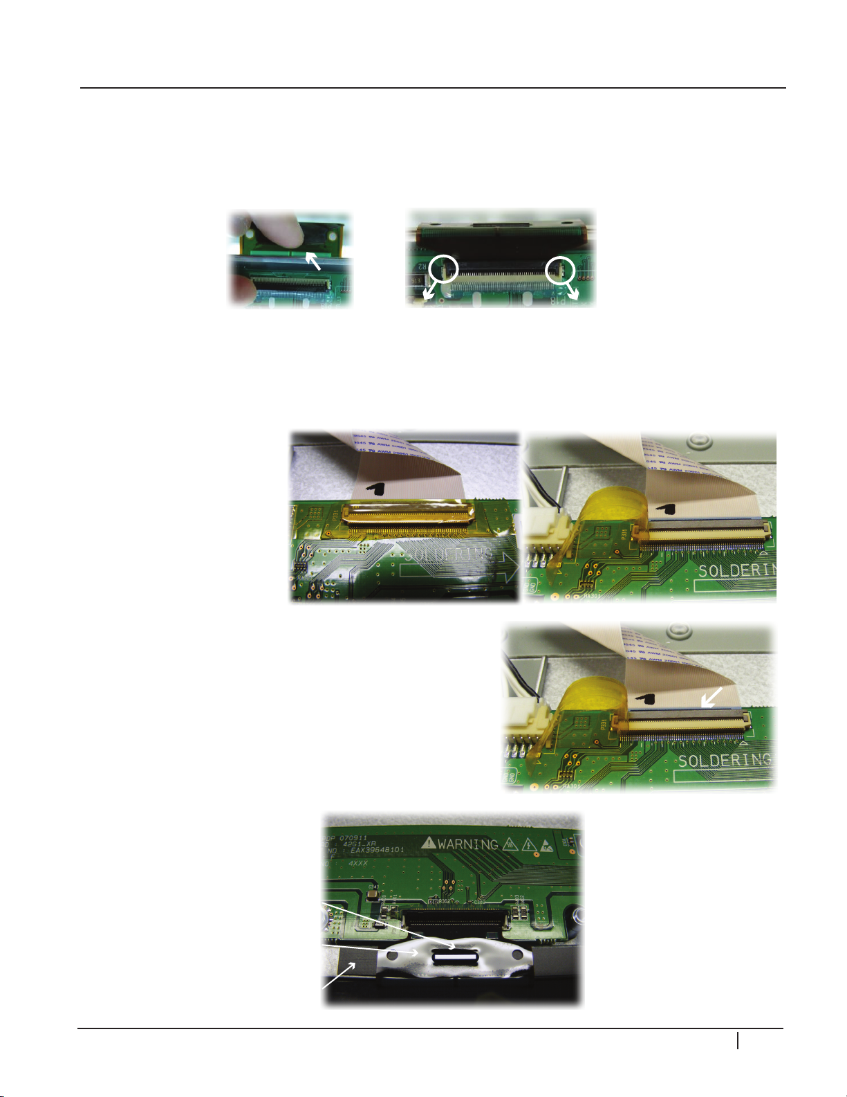
DISASSEMBLY
Cushion
TCP
Flexible Ribbon Cable
TCP CONNECTOR REMOVAL
Lift up the lock as shown by arrows. The Lock can be easily broken, it needs to be handled
carefully. Pull TCP apart as shown by arrow. TCP Film can be easily damaged, handle with
care.
P232 & P331 CONNECTOR REMOVAL
After removing the back cover, lifting the Main board out of the way, removing 15 screws
from the heat sink covering the TCPs, and removing the heat sink, the X-Drive boards
can be removed.
Pe el t he ta p e o ff
the c onnectors a nd
gently pry the locking
mechanism upward.
Gently pry the locking mechanism upward on all
TCP connectors P201-206 or P301-306. Carefully
lift the TCP ribbon up and off the cushion and out
of the way.
5
0
P
G
2
0
PDP Training - Fall 2008 67
Page 70
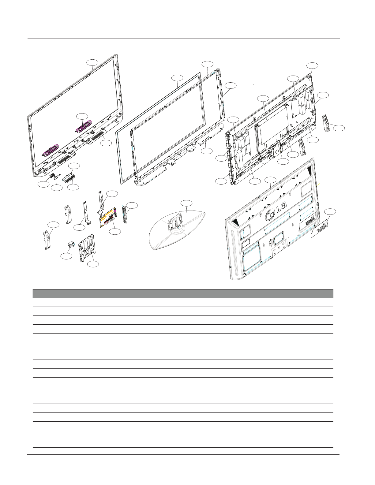
DISASSEMBLY
900
304
302
303
305
300
120
570
560
561
571
301
250
200
209
580
207
208
201
204
205
206
202
203
602
601
240
501
590
603
520
400
401
50PG20 EXPLODED VIEW
5
0
P
G
2
0
Location Part Num Description Location Part Num Description
120 EAB42609901 Full Range Speaker 304 AJJ35805301 Bottom Filter Support
200 EAJ41970601 PDP Panel (PDP Module) 305 MDJ42351002 Glass Filter
201 EBR38301801 Control board (CTRL) 400 ACQ35758902 Back Cover
202 EBR38374701 Top Y-drive (YDRV TOP) 401 MCK41119502 Rear Cover
203 EBR38374801 Bottom Y-Drive (YDRV BTM) 501 MJH40272501 Supporter/Module Guide
204 EBR38299201 Left X-Drive (XRLB) 520 EBR42710401 Main/Digital PCB
205 EBR38299501 Center X-Drive (XRCB) 560 EBR43329001 Sub PCB
206 EBR38299701 Right X-Drive (XRRB) 561 MBG41119901 Control Buttons
207 EBR38374401 Y-Sustain (YSUS) 570 EBR43329401 Preamp PCB
208 EBR38374501 Z-Sustain (ZSUS) 571 ABA36912801 Bracket Assembly
209 EBR40167201 Z-Sustain Sub (ZSUS SUB) 580 EAY41360901 Power Supply (SMPS)
240 AJJ35707601 Bottom Right Vertical Support 590 EAM35012711 AC Line Filter
250 AJJ35707501 Top Right Vertical Support 601 ABA35619217 Side Input Bracket Assembly
300 ABJ35754707 Cabinet Assembly 602 MGJ41164505 Main board Supporter
301 ABA36825004 Speaker Bracket Assembly 603 MGJ41163803 Main board Supporter CH
302 AJJ35805401 Right Filter Support 900 AAN36676501 Stand (Base Assembly)
303 AJJ35805201 Top Filter Support
Part numbers subject to change.
Check GCSC (aic.lgservice.com) for
the current part numbers.
68 PDP Training - Fall 2008
Page 71
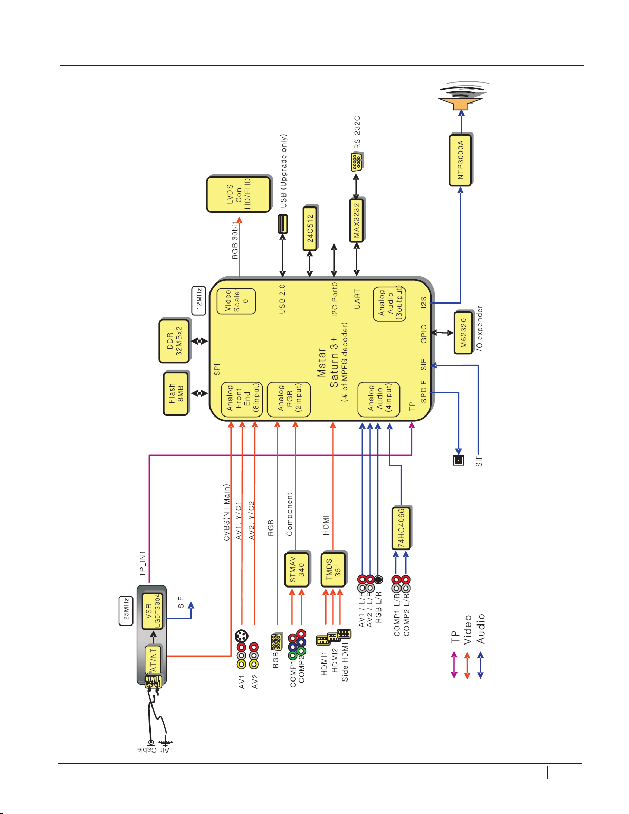
BLOCK DIAGRAM
DISASSEMBLY
5
0
P
G
2
0
PDP Training - Fall 2008 69
Page 72
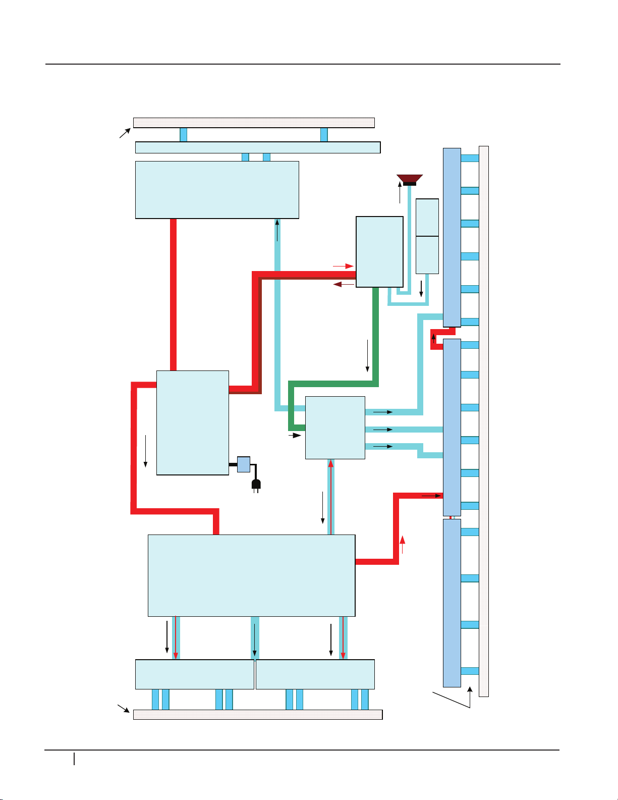
DISASSEMBLY
P110
P120
P230
P240
P210
P220
P130
P140
50PG20 SIGNAL and VOLTAGE DISTRIBUTION DIAGRAM
Display Panel
Horizontal Address
P100
5V
Drive Signal
Y-SUS
PWB
P206
P209
P208
P102
P210
P200
M5V, Va, Vs
P801
P803
CN101
STB +5V, 16V, 5V
SMPS
Turn On
Commands
SMPS PWB
AC
Input
Filter
P1
SMPS OUTPUT VOLTAGES
STB +5V, 16V, 5V
Drive Signals
Logic Signals
P160
AC Voltage Det
P701
P302
P303
CN701
MAIN
PWB
Speakers
Control
Keys
Power
Keys
X-PWB-RightX-PWB-Left
P101 P102 P103 P104 P201 P202
RGB Logic Signals
15V, Va
RGB Logic Signals
3.3V
CONTROL
PWB
P162
LVDS
Y Drive
Upper PWB
Z SUS
PWB
P151
P121
P6
P8
P241
P232
Display Panel Vertical Address
IR
Display Panel
Horizontal Address
M5V, Va, Vs
P802
P163
P2
P3
P4
P5
P10
P11
P161
P203 P204 P205 P206 P301 P302 P303 P304 P305 P306
P233P121
P242
P331
P311
P211
15V, Va
P207
P208
Drive Data
Clock (i2c)
5V
Drive Data
P200
Y Drive
Lower PWB
5V
Display Panel
Vertical Address
SIGNAL AND VOLTAGE BLOCK DIAGRAM
5
0
P
G
2
0
70 PDP Training - Fall 2008
Page 73
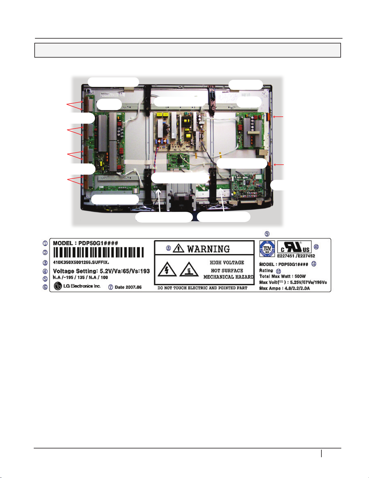
CIRCUIT DESCRIPTIONS
Y-Sus
Control (Logic)
Upper Y-Drive
Voltage Label
Main (Digital)
Panel ID
Power Supply
Z-Sus
Right X-Board
Left X-Board
Side Inputs
Lower Y-Drive
FPC
FPC
FPC
FPC
FPC
FPC
Center X-Board
CIRCUIT DESCRIPTIONS 50PG20
INTRODUCTION
PANEl lAbEl
(1) Model Name
(2) Bar Code
(3) Manufacture No.
(4) Adjusting Voltage DC, Va, Vs
(5) Adjusting Voltage (Set Up/-Vy/Vsc/Ve/Vzb)
(6) Trade name of LG Electronics
(7) Manufactured date (Year/Month)
(8) Warning
(9) TUV Approval Mark
(10) UL Approval Mark
(11) UL Approval No.
(12) Model Name
(13) Max. Watt (Full White)
(14) Max. Volts
(15) Max. Amps
5
0
P
G
2
0
PDP Training - Fall 2008 71
Page 74
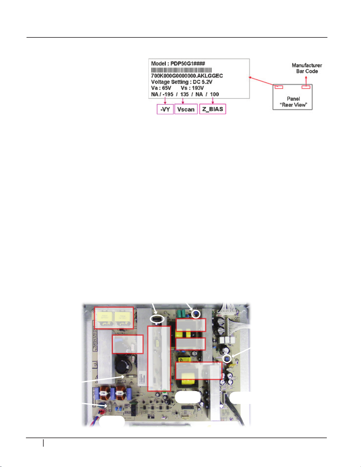
CIRCUIT DESCRIPTIONS
F801
340V Fuse
10Amp/230V
F101
340V Fuse
10Amp/230V
Standby
Source
PFC
Circuit
CN 101
AC Input
VS Source
VA Source
U701
Sub Micon
P803
To Main
VA VR902
380V
Source
16V, 12V, 5V, 3.2V
Source
VS VR901
P801
To Y-Sus
P802
To Z-Sus
U801
Regulation
ADJUSTMENT ORDER **IMPORTANT**
DC vOlTAGE ADJUSTMENTS
1) SMPS board: Va/Vs (Do
SMPS first).
2) Y-Sus board: Adjust Vscan,
-Vy.
3) Y-Sus board: Adjust Zbias
It is critical that the DC Voltage adjustments be checked whenever troubleshooting
a problem. Especially when: The SMPS, Y-Sus, or Z-Sus are replaced. Also when the
panel is replaced (since the SMPS does not come with new panel), or a picture issue is
encountered.
WAvEFORM ADJUSTMENTS
1) Y-Sus board: Ramp Up, Ramp Down.
Only necessary when: The Y-Sus board is replaced, a “Mal-Discharge” problem is
encountered, or an abnormal picture issues is encountered.
5
0
P
G
2
Always refer to the Voltage Sticker located on the back of the panel, in the upper lefthand side for the correct voltage levels for the VA, VS, -VY, Vscan, and Z-Bias as they will
vary from panel to panel. The 5V VCC is pre-adjusted and sealed.
POWER SUPPLY
Check the sticker on the upper left side to confirm origin of the panel or the white label on
the Power Supply itself to identify the board part number. We will examine the operation
of the EAY41360901.
0
72 PDP Training - Fall 2008
Page 75
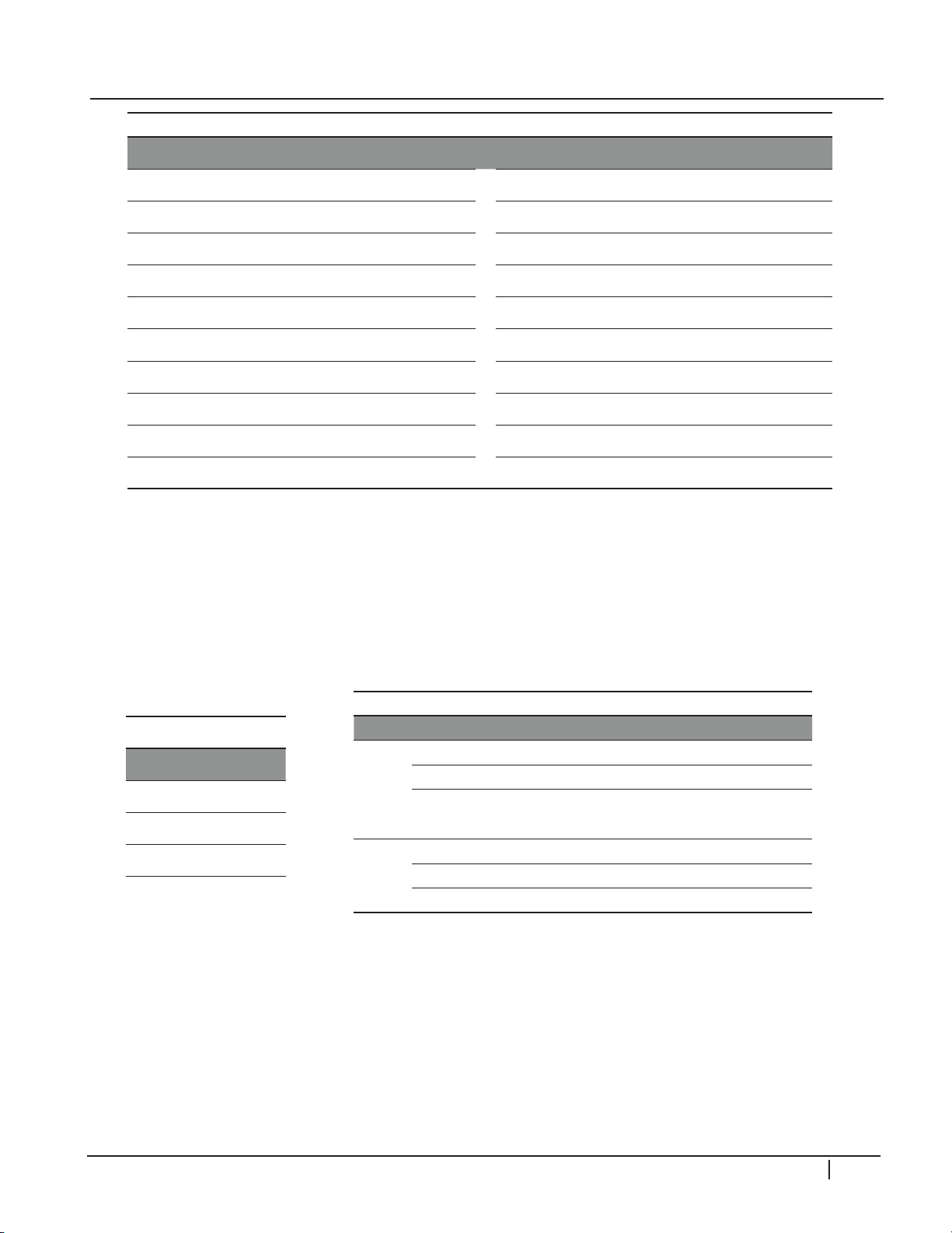
CIRCUIT DESCRIPTIONS
P802 “SMPS” to P3 “X-Sus”
Pin Label Stby Run Resistance Pin Label Stby Run Resistance
1 Vs 0V 192V OL 1 Vs 0V 192V OL
2 Vs 0V 192V OL 2 Vs 0V 192V OL
3 nc nc nc nc 3 Gnd Gnd Gnd nc
4 Gnd Gnd Gnd Gnd 4 Gnd Gnd Gnd Gnd
5 Gnd Gnd Gnd Gnd 5 Gnd Gnd Gnd Gnd
6 Va 0V 65V OL 6 Va 0V 65V OL
7 Va 0V 65V OL 7 Va 0V 65V OL
8 Gnd Gnd Gnd Gnd 8 Gnd Gnd Gnd Gnd
9 M5V 0V 5V .897V 9 M5V 0V 5V .897V
10 M5V 0V 5V .897V 10 M5V 0V 5V .897V
Adjustments
Voltage Location
VA RV901
VS RV951
M5V VCC Fixed
SMPS Outputs
Board Voltage Description
VS Drives the display panel Horizontal Grid
Y-Sus
/Z-Sus
Main
VA Responsible for display panel Vertical Grid
M5V VCC
16V Audio B+ Supply
12V Signal Processing Circuits and Fan Drive
5V Signal Processing Circuits
Used to develop Bias Voltages on the Y-Sus,
X-Drive, and Control boards
5
0
P
G
2
0
PDP Training - Fall 2008 73
Page 76

CIRCUIT DESCRIPTIONS
PSU OPERATION
AC Voltage is supplied to the SMPS board at connector SC101 from the AC Input Filter.
Standby 5V is developed from the 330V source supply (which during standby measures
155V with relation to AC Ground). This supply is also used to generate all other voltages
on the SMPS. The 5V (standby) voltage is routed to the Sub Micon (U701) on the SMPS
and through P803 to the Main board for Micon operation ( IC100).
AC detect Pin 18 of P803 is generated on the SMPS by monitoring the AC input and
rectifying a small sample voltage. This AC Detect voltage is routed to the Sub Micon
(U701) on the SMPS and the Micon (IC100) located on the Main board and is used as
a basic “SMPS OK” signal.
When the Micon (IC100) on the Main board receives an “ON“ Command from either
the Keyboard or the Remote IR Signal it outputs a high to RL-ON which enters the SMPS
board at Pin 19 of P803. The RL-ON Voltage is sensed by the Sub Micon (U701) circuit
which causes the Relay Drive Circuit to close Relay RL101 bringing the PFC source up to
full power by increasing the 155V standby to 330V. At this time the 16V source becomes
active and sent to the Main board via P803.
5
0
P
G
2
0
The next step is for the Micon (IC100) on the Main board to output a high on M5V_ON
line to the SMPS at P803 Pin 21 which is sensed by the Sub Micon IC (U701) on the
SMPS turning on the 5V VCC line. The last step to bring the supply to “Full Power” occurs
when the Micon (IC100) on the Main board brings the VS-ON line high at Pin 20 of
P803 on the SMPS board which when sensed by the Sub Micon IC (U701) turns on the
VA and VS Supplies (VA is brought high before VS).
Note: if a voltage is missing, check for proper resistance before proceeding.
TROUblEShOOTING TIPS
Understanding the power on sequence when troubleshooting a possible Power Supply
failure will simplify the process of isolating which circuit board failed to operate properly.
In this section we will investigate the power on sequence and examine ways to locate
quickly where the failure occurred.
Check the Power On LED for operation. A red LED indicates a presence of 5V STB and
AC-ON/DETECT. Failure of the Power ON LED to light is an indication of loss of 5V STB
or AC ON/ Detect remember the 5V STB and AC-ON/DETECT are developed on the
SMPS and sent to the Main board.
Listen for a relay click, the click of the relay is an indication of RL-ON going high. RL-ON
is sent from the Main board to the SMPS and when present the U701 controls the relay
operation. RL-ON going high and no relay is a failure of the SMPS. RL-ON staying low is
a failure of the Main board.
74 PDP Training - Fall 2008
Page 77

CIRCUIT DESCRIPTIONS
The next step of operation calls for the M5V_ON line from the Main board to the SMPS to
go high on P803 pin 21. A high on the M5V_ON Line activates the 5V VCC line. Loss of
5V VCC results in no raster, no display panel reset, no Y/Z Control or X-board operation.
Loss of 5V VCC and M5V_ON going high could be caused by any of these boards or
failure of the SMPS. M5V_ON staying low indicates a problem on the Main board.
VS-ON is the last step of the power sequence and is responsible for bringing the VS
and VA Voltages up. The VS-ON signal pin 20 P803 is sent from the Main board to the
SMPS as a high, VS and VA and full operation of the display panel are now enabled. Loss
of VS-ON results in loss of VA and VS and no raster, no panel display reset but audio
would be present. If VS-ON went high and VS and VA where missing the problem could
be caused by a failure on the SMPS or a circuit using these voltages. A resistance check
should narrow the possible failures quickly.
5
0
P
G
2
0
PDP Training - Fall 2008 75
Page 78
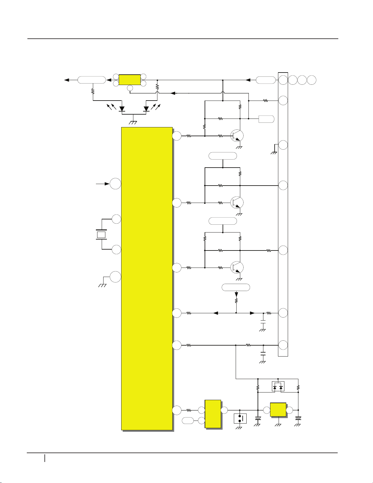
CIRCUIT DESCRIPTIONS
76
Pulse
R1045
RL-ON
Pull-Down
Va/Vs-On
166
Pull-Down
R137
M5V-On
115
INT
R184
AC-DET
AC-DET
I
O
1
1A
2
1Y
14
3.3V
128
HW-RESET
P701
18
R727
R764
R717
R723
R718
R715
19
R763
RL-ON
R711
R6070
R716
+5V-General
21
0ohm
RL-ON
M5V-On
AC-DET
VS-On
80
Pull-Up
R126
5V-MNT
17
5V-DET
R722
R720
R142
R141
C142
C143
68010K
SW100
Vcc
R135
167
R136
R732
R736
R729
20
0ohm
Q704
R6071
+5V-General
+5V-General
Q702
C713
Q703
C701
IC101
D100
IC104
254
255
X100
12Mhz
Vcc
9
10
11
12
+5V-ST
Level Shifter
LD703
Set Off +5VST Red
Set On 5VGen Amber
22
Gnd
Q706
+5V-General
4
6
3
5
RL-ON
LD703
1.8V
1.6V
IC100
RedGreen
2
MICRO CONTROl OF ThE POWER SUPPlY
5
0
P
G
2
0
76 PDP Training - Fall 2008
Page 79
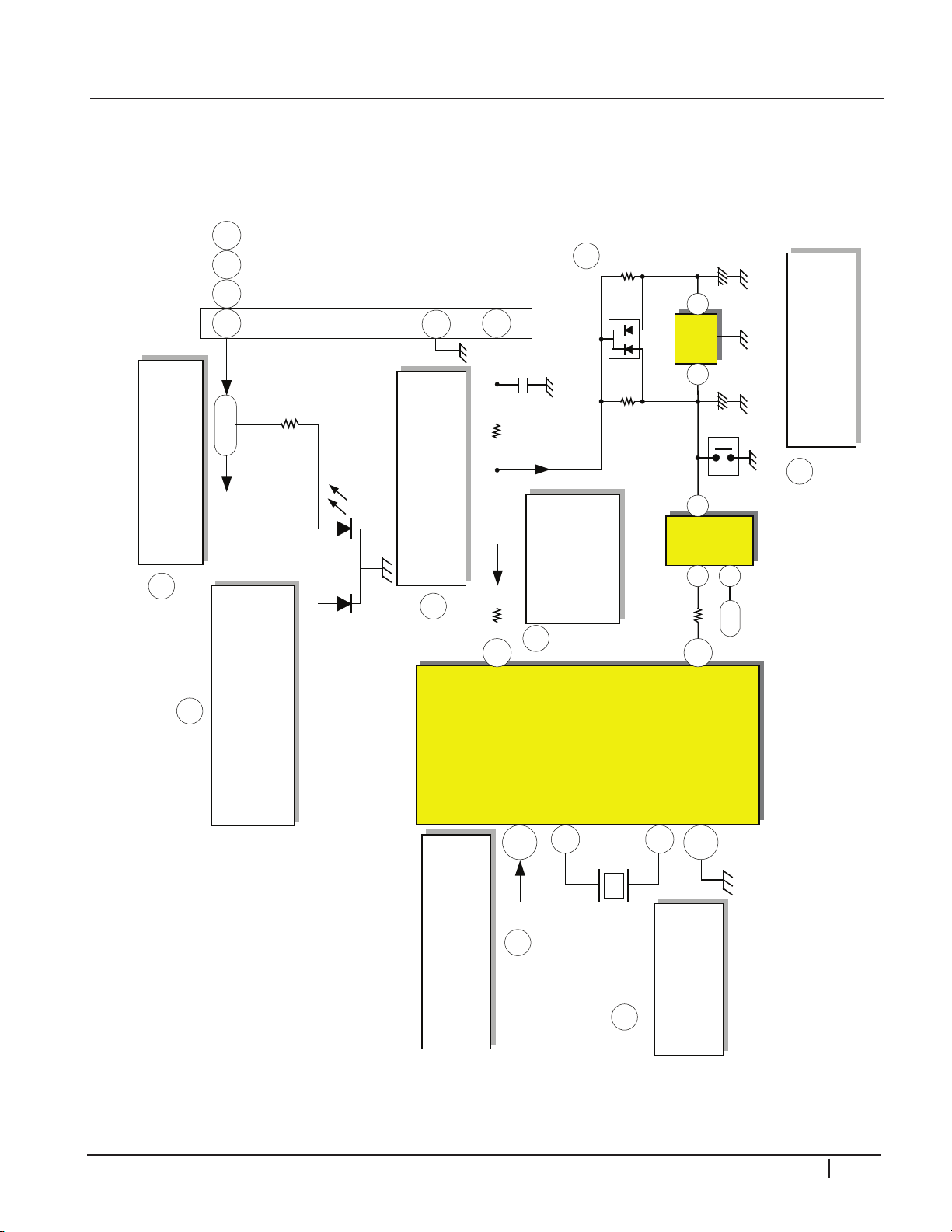
115
INT
R184
AC-DET
AC-DET
IO1
1A
2
1Y
14
3.3V
128
HW-RESET
P701
18
R727
AC-DET
R142
R141
C142
C143
68010K
SW100
Vcc
R135
C713
IC101
D100
IC104
254
255
X100
12Mhz
Vcc
9 10 11 12
Gnd
22
IC100
+5V-ST
RL-ON
LD703
1.8V
Green
50PG20 Power Supply Controls from Micro Side 1
st
STEP
5V-SBY Arrives
from SMPS
AC-DET Arrives
from SMPS
Micro Receives Vcc
AC-DET creates
Micro Reset
Oscillator
starts
LED703 receives
5VST and glows Green
A
B
B
A
A
D
A
C
SW 100 Manual
Micro. Reset
AC-DET is
Monitored
by uP
MICRO CONTROl OF ThE POWER SUPPlY STEP 1
CIRCUIT DESCRIPTIONS
5
0
P
G
2
0
PDP Training - Fall 2008 77
Page 80
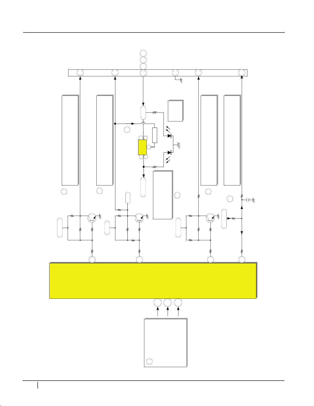
CIRCUIT DESCRIPTIONS
P701
118
9 10 11 12
+5V-ST
Q706
+5V-General
Level Shifter
4
6
LD703
1.8V1.6V
Red
5
50PG20 Power Supply Controls from Micro Side 1
st
STEP
119
KEY
CONTROLS
IC100
114
REMOTE
IR In
R764
VS-On
76
Pull-Up
R126
5V-MNT
17
5V-DET
R722
R720
167
R136 R732
R736
R729
20
0ohm
Q704
R6071
+5V-General
+5V-General
C701
Green
Appears Amber
166
R137
M5V-On
R711
R6070
R716
+5V-General
21
0ohm
M5V-On
Q702
76
Pulse
R1045
RL-ON
R717
R723
R718
R715
+5V-ST
19
R763
RL-ON
RL-ON
Q703
22
RL-ON
To other
circuts
Receives
Power On
Command
From Side Keys or
Remote
Outputs Relay On (RL-ON) command
Turns on Power Supply Relay
Turns on Q706
Creates 5V General
Lights
Amber
Outputs M5V On command
Turns on 16V/12V Power Supplies
5V General allows 5V Detect
To be Generated
Outputs VS-On which turns on Va and
Vs in the Power Supply
A
E
B
D
F
C
B
3
2
MICRO CONTROl OF ThE POWER SUPPlY STEP 2
5
0
P
G
2
0
78 PDP Training - Fall 2008
Page 81
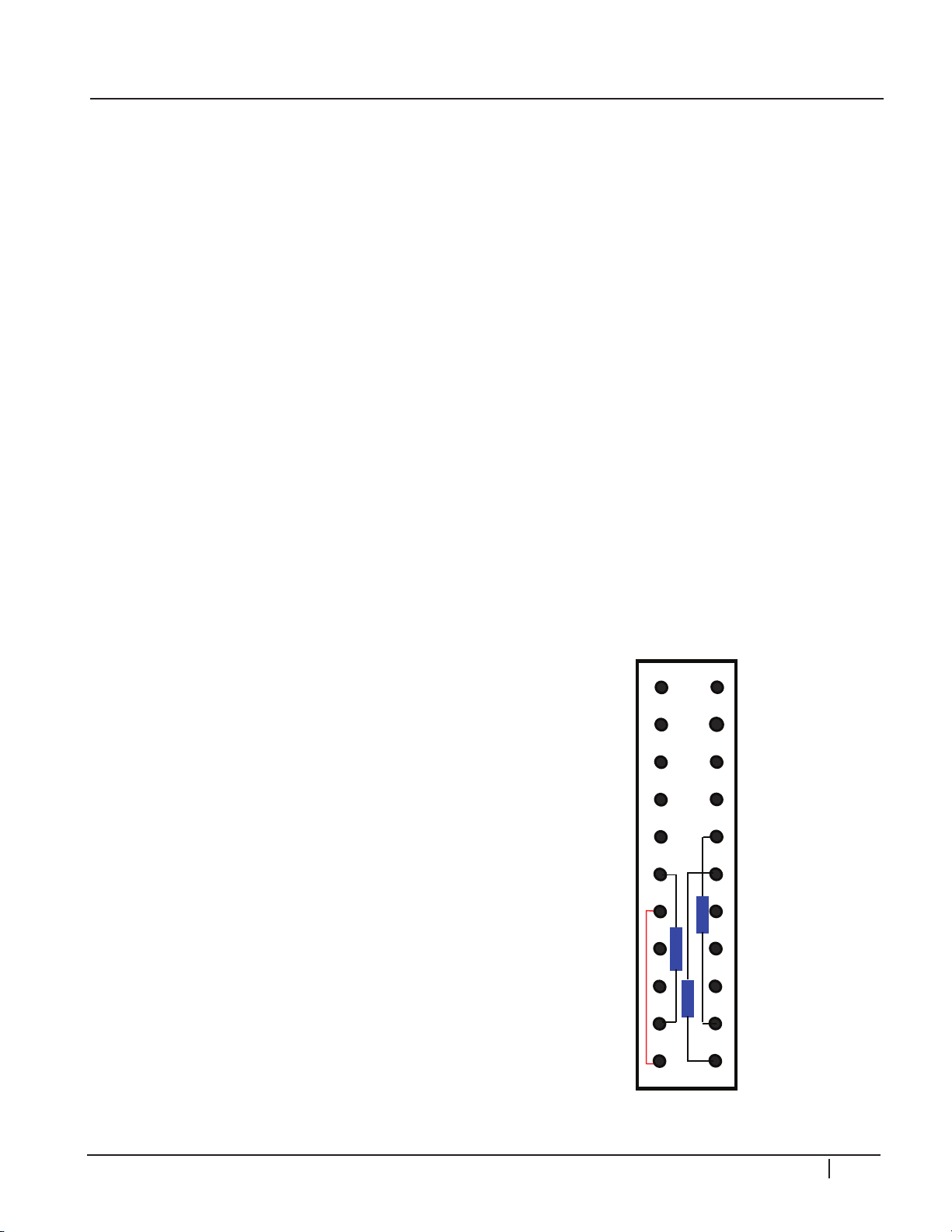
CIRCUIT DESCRIPTIONS
2
4
6
8
10
12
14
16
18
22
16V
Gnd
NC
Gnd
5VSTB
5VSTB
Gnd
Gnd
AC Det
VS_ON
Auto Gnd
2
4
6
8
10
12
14
16
18
22
16V
Gnd
NC
Gnd
5VSTB
5VSTB
Gnd
Gnd
AC Det
VS_ON
Auto Gnd
20
3
5
7
9
11
13
15
17
19
21
Gnd
NC
Gnd
5VSTB
5VSTB
Gnd
Gnd
5_V Det
RL_ON
M5V_ON
1
15V
3
5
7
9
11
13
15
17
19
21
Gnd
NC
Gnd
5VSTB
5VSTB
Gnd
Gnd
5_V Det
RL_ON
M5V_ON
1
15V
P803
SMPS STATIC TEST
This test can confirm the proper operation of the SMPS without the need to exchange
the board for testing purposes. This Power Supply can operate in a no load state. This
means that by applying AC power to SC101 and all other plugs disconnected, this
power supply will come up and run. Simply removing P803 (Lower right-hand side of the
board) will cause the “AUTO” pin 22 to go high from its normal low state. This will allow
the Power Supply to go to full power on when AC is applied and there are no excessive
loads on the P801 or P802 connectors going to the Y-Sus and Z-Sus boards. Remove
AC between each test step.
If the Y-Sus and Z-Sus boards are working OK, the power supply will fire up and run and
“Reset” will be visible. Shorting the Auto Pattern Gen. test points at this time should
result in seeing test patterns on the screen.
If either Y-Sus or Z-Sus is causing the power supply to shutdown, unplug the Z-Sus. This
will allow the Y-Sus to function. If you unplug the Y-Sus from the SMPS, the Z-Sus will
not run due to a loss of 5V to the Control board from the Y-Sus circuits.
For a “Stand-Alone” static test for the Power Supply, apply the usual 2 100 Watt light
bulb test on the Vs output line for a simulated load. If the power supply operates in this
condition, it is assured it can maintain its output power under load.
To turn power supply on in stages:
1) Ground the Auto Ground (Pin 22) on
P813.
2) AC Power Applied AC Det (Pin 18) and 5V
STB (Pins 9 ~ 12) are 5V.
3) 100Ω ¼ watt resistor added from 5V STB
(Pins 9 ~ 12) to RL ON (Pin 19) closes relay
RL101 turning on the 16V Supply.
4) 100Ω ¼ watt resistor added from 5V STB
(Pins 9 ~ 12) to M5V_ ON (Pin 21) brings
the 5V VCC line high.
5) 100Ω ¼ watt resistor added from 5V STB
(Pins 9 ~ 12) to VS _ON (Pin 20) brings
the VA and VS Lines high.
5
0
P
G
2
0
PDP Training - Fall 2008 79
Page 82
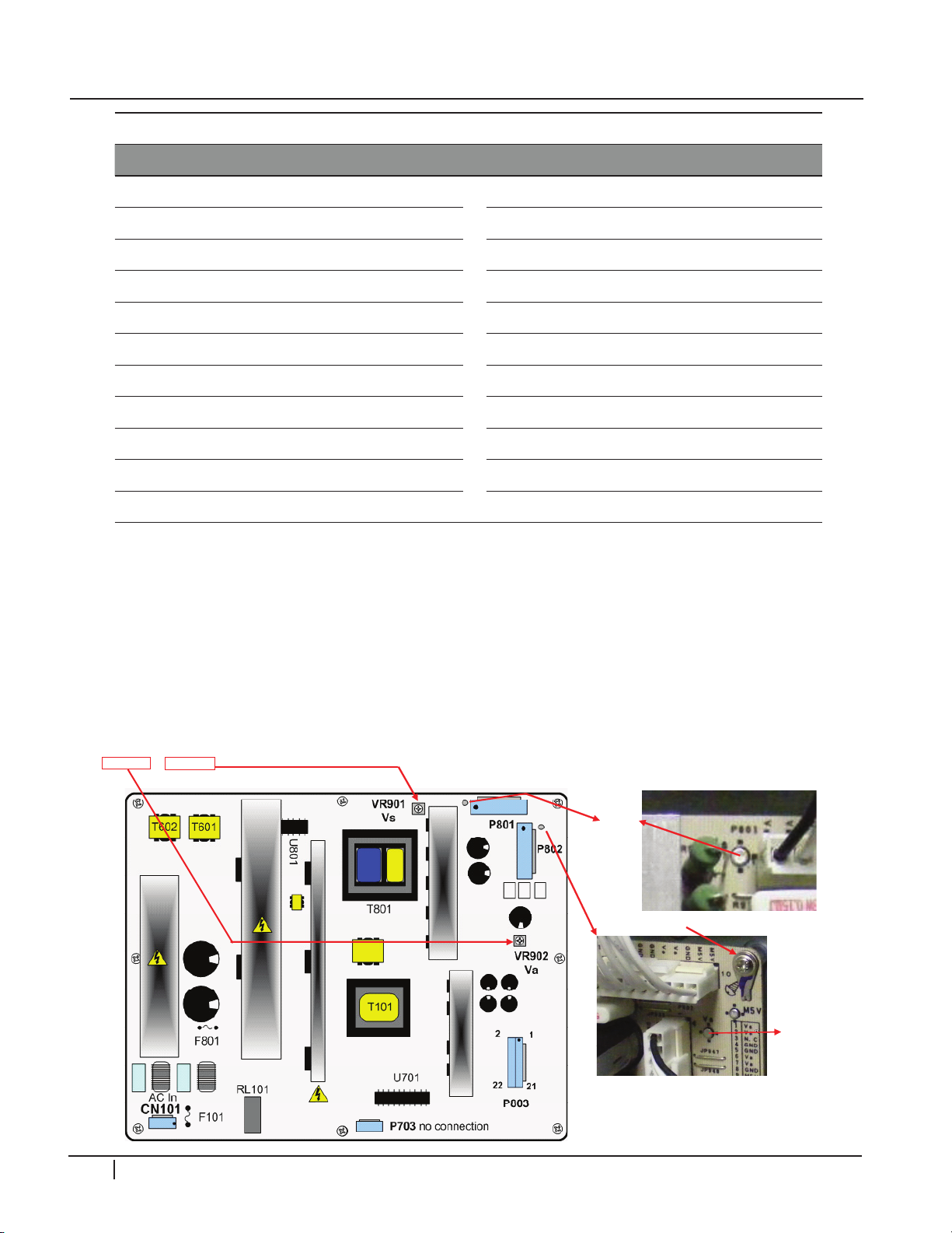
CIRCUIT DESCRIPTIONS
Model : PDP50G1####
|||||||||||||||||||||||||||||||||||||||||||
700K000G0000000.AKLGGEC
Voltage Setting : DC 5.2V
Va : 65V Vs : 193V
NA / -195 / 135 / NA / 100
Va
TP
Vs
TP
GND
P803 “SMPS” to P701 “Main”
Pin Label Stby Run No Load Resistance Pin Label Stby Run No Load Resistance
1 15V 0V 16V 16V 2.26V 2 15V 0V 16V 16V 2.6V
3 Gnd Gnd Gnd Gnd Gnd 4 Gnd Gnd Gnd Gnd Gnd
5 12V 0V 12V 12V 2V 6 12V 0V 12V 12V 2V
7 Gnd Gnd Gnd Gnd Gnd 8 Gnd Gnd Gnd Gnd Gnd
9 5V 5V 5V 5V 1.7V 10 5V 5V 5V 5V 1.7V
11 5V 5V 5V 5V 1.7V 12 5V 5V 5V 5V 1.7V
13 Gnd Gnd Gnd Gnd Gnd 14 Gnd Gnd Gnd Gnd Gnd
15 Gnd Gnd Gnd Gnd Gnd 16 Gnd Gnd Gnd Gnd Gnd
17 5_V Det .15V 5V 5V 1.56V 18 AC Det 5V 5V 5V 2.56V
19 RL_On 0V 4.5V 0V 2.6V 20 Vs_On 0V 3.2V 0V 2.7V
21 M5V_ON 0V 3.2V 0V 2.6V 22 AUTO 0V 0V 5V 2.1V
5
0
P
G
2
0
vS/vA ADJUSTMENTS
This Power Supply will come up and run with “NO” load. Use Full White Raster. Pull P803
and apply AC power. The power supply starts and Y and Z -SUS Runs. Pull “802” Y-Sus
Runs but not Z-Sus . Pull “801” and Y/Z-SUS will not Run.
80 PDP Training - Fall 2008
Page 83
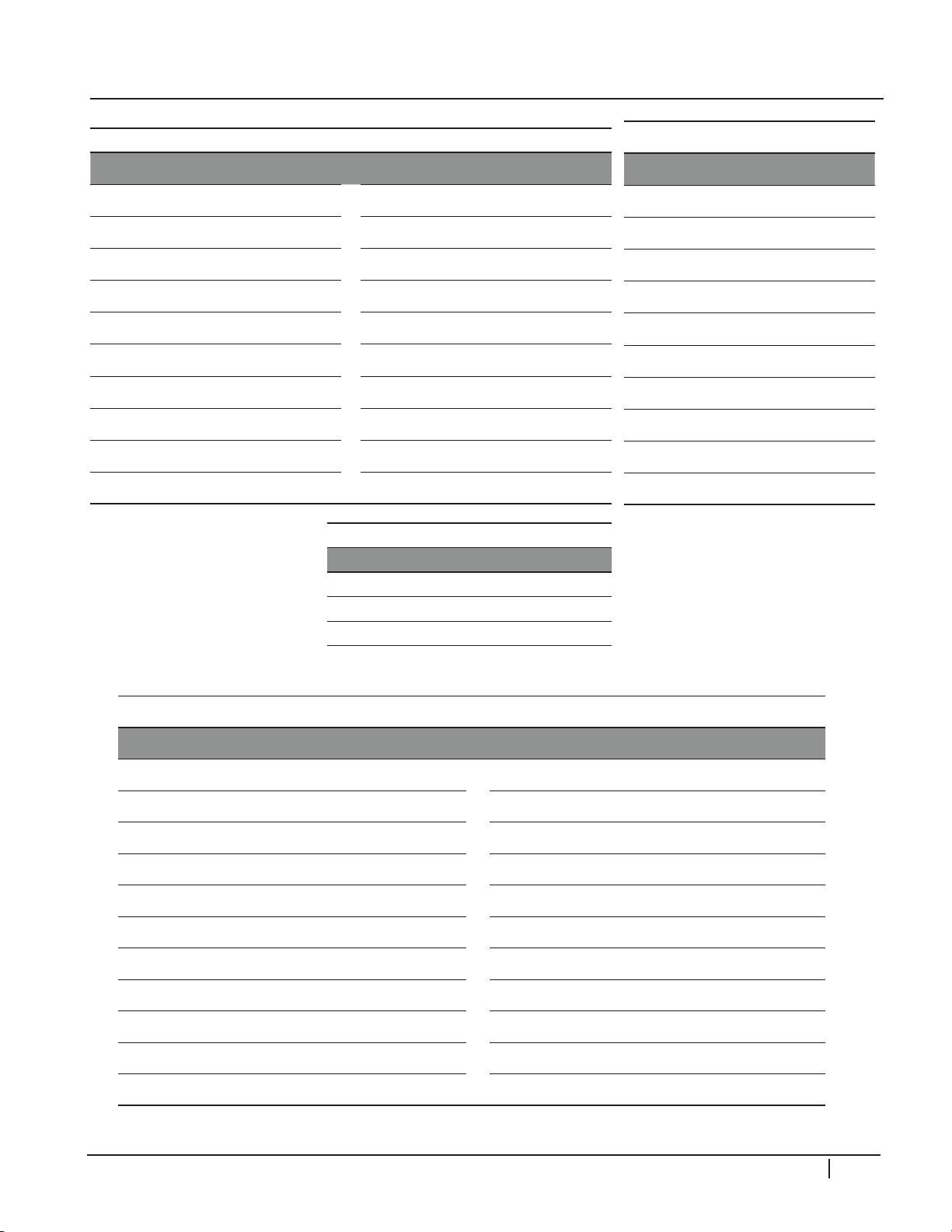
CIRCUIT DESCRIPTIONS
P802 “SMPS” to P3 “X-Sus”
Pin Label Stby Run Resistance Pin Label Stby Run Resistance
1 Vs 0V 192V OL 1 Vs 0V 192V OL
2 Vs 0V 192V OL 2 Vs 0V 192V OL
3 nc nc nc nc 3 Gnd Gnd Gnd nc
4 Gnd Gnd Gnd Gnd 4 Gnd Gnd Gnd Gnd
5 Gnd Gnd Gnd Gnd 5 Gnd Gnd Gnd Gnd
6 Va 0V 65V OL 6 Va 0V 65V OL
7 Va 0V 65V OL 7 Va 0V 65V OL
8 Gnd Gnd Gnd Gnd 8 Gnd Gnd Gnd Gnd
9 M5V 0V 5V .897V 9 M5V 0V 5V .897V
10 M5V 0V 5V .897V 10 M5V 0V 5V .897V
CN101 “Power Supply” from AC In
Pin Standby Run Resistance
1 120VAC 120VAC 480K
2 N/C - -
3 120 VAC 120VAC 480K
P801 “PSU” to P209 “Y-Sus”
Pin Label Stby Run Resistance
1 Vs 0V 192V OL
2 Vs 0V 192V OL
3 nc nc nc nc
4 Gnd Gnd Gnd Gnd
5 Gnd Gnd Gnd Gnd
6 Va 0V 65V OL
7 Va 0V 65V OL
8 Gnd Gnd Gnd Gnd
9 M5V 0V 5V 0.897V
10 M5V 0V 5V 0.897V
P803 “SMPS” to P701 “Main”
Pin Label Stby Run No Load Resistance Pin Label Stby Run No Load Resistance
1 15V 0V 16V 16V 2.26V 2 15V 0V 16V 16V 2.6V
3 Gnd Gnd Gnd Gnd Gnd 4 Gnd Gnd Gnd Gnd Gnd
5 12V 0V 12V 12V 2V 6 12V 0V 12V 12V 2V
7 Gnd Gnd Gnd Gnd Gnd 8 Gnd Gnd Gnd Gnd Gnd
9 5V 5V 5V 5V 1.7V 10 5V 5V 5V 5V 1.7V
11 5V 5V 5V 5V 1.7V 12 5V 5V 5V 5V 1.7V
13 Gnd Gnd Gnd Gnd Gnd 14 Gnd Gnd Gnd Gnd Gnd
15 Gnd Gnd Gnd Gnd Gnd 16 Gnd Gnd Gnd Gnd Gnd
17 5_V Det .15V 5V 5V 1.56V 18 AC Det 5V 5V 5V 2.56V
19 RL_On 0V 4.5V 0V 2.6V 20 Vs_On 0V 3.2V 0V 2.7V
21 M5V_ON 0V 3.2V 0V 2.6V 22 AUTO 0V 0V 5V 2.1V
5
0
P
G
2
0
PDP Training - Fall 2008 81
Page 84
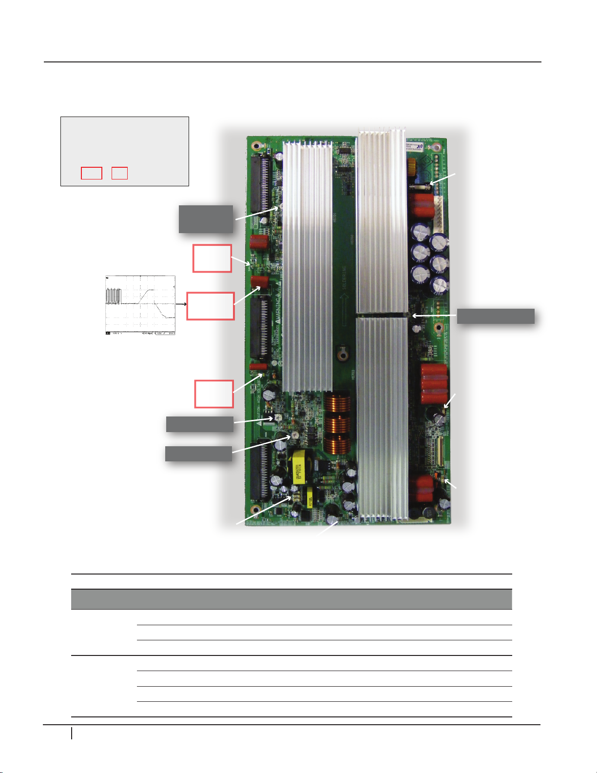
P206
To Y-Drive
VR601
V-Set Down
C213
Y-Drive TP
VSC ADJ R501
P200
To Y-Drive
R201
-VY TP
R202
VSC TP
-VY ADJ R502
P102
Logic Signals From
Control 5V & Va to
CenterX-Board
V-Set Up VR302
FS202 (5V)
125V 10A
FS701 (Va)
125V 10A
P209
Vs/Va Input
from SMPS
FS201 (Vs)
Glass 250V 4A
P207
To Y-Drive
P208
To Y-Drive
FS502 125V 1.5A
FS501 125V 1.5A
FS504 125V 1.5A
(All -90V)
FS503 (5V)
125V 5A
P210
Model : PDP 50G1####
||||||||||||||||||||||||||||||||||||||||||||||||||||
700K000G0000000 .AKLGGEC
Voltage Setting : DC 5.2V
Va : 65V Vs : 193 V
NA / -195 / 135 / NA / 100
VSC
-VY
Model : PDP 50G1####
||||||||||||||||||||||||||||||||||||||||||||||||||||
700K000G0000000 .AKLGGEC
Voltage Setting : DC 5.2V
Va : 65V Vs : 193 V
NA / -195 / 135 / NA / 100
VSC
-VY
CIRCUIT DESCRIPTIONS
Y-SUSTAIN
P206, P207, and P208 provide logic (drive) signals to the Y-Drive boards.
5
0
P
G
2
Board Voltage
SMPS
0
Developed on
Y/Z-Sus
82 PDP Training - Fall 2008
SMPS Outputs
VS Supplies the Horizontal Grid
VA Supplies the Vertical Grid
VCC 5V 5V Supplies Bias to Y/Z-Sus, Control, and X-Boards
-VY -VY Sets the Negative excursion of the Y SUS Drive Waveform
V-Set Up Ramp UP sets Pitch of the Top Ramp of the Drive Waveform
V-Set Down V-Set Down sets the Pitch of the Bottom Ramp of the Drive Waveform
VSC VSC Set the amplitude of the complex waveform.
Page 85
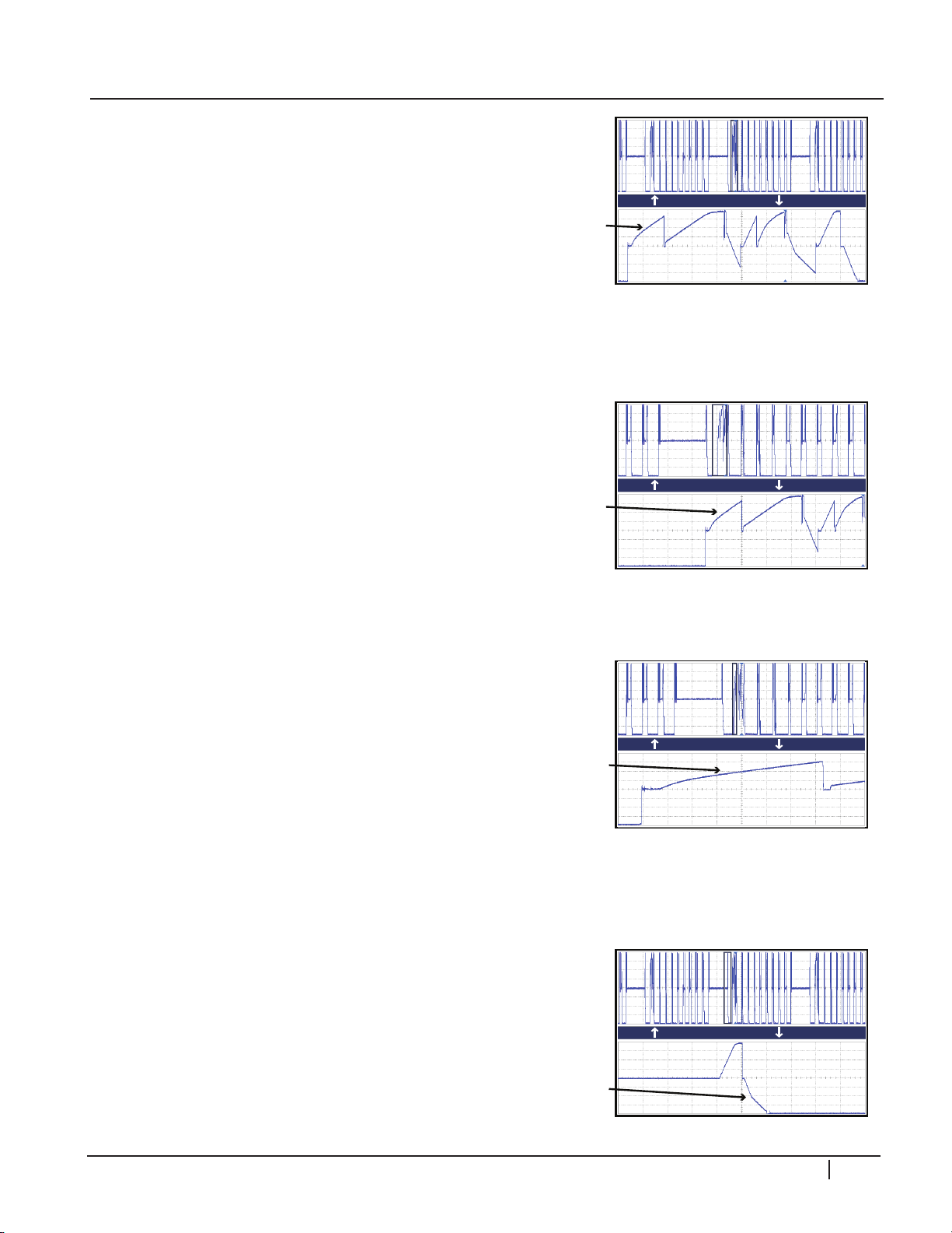
Y-DRIvE SIGNAl FOR vSETUP RAMP-UP
5ms
100us
Area
to be
adjusted
5ms
100us
Area
to be
adjusted
5ms
100us
Area
to be
adjusted
5ms
100us
Area to be
adjusted
expanded
As an example of how to lock in to the Y-Drive
Waveform. Figure 1 top shows the signal locked
in at 5ms per/div. The outlined signal for Vsetup
is outlined within the Waveform. At 100uSec
per/division, the waveform to use for Vsetup Is
now isolated.
At 2ms per/div. the outlined signal for Vsetup
is now easier to recognize. It is outlined within
the Waveform. At 100uSec per/division, the
waveform to use for Vsetup Is now isolated.
CIRCUIT DESCRIPTIONS
At 2ms per/div. the outlined signal for Vsetup
is now clearly visible. It is outlined within
the Waveform. At 20uSec per/division, the
adjustment for Vsetup can be made.
As an example of how to lock in to the Y-Drive
Waveform. Figure 1 top shows the signal
locked in at 5ms per/div. The outlined signal
for Vsetdn is outlined within the Waveform. At
100uSec per/division, the waveform to use for
Vsetdn is now isolated.
5
0
P
G
2
0
PDP Training - Fall 2008 83
Page 86
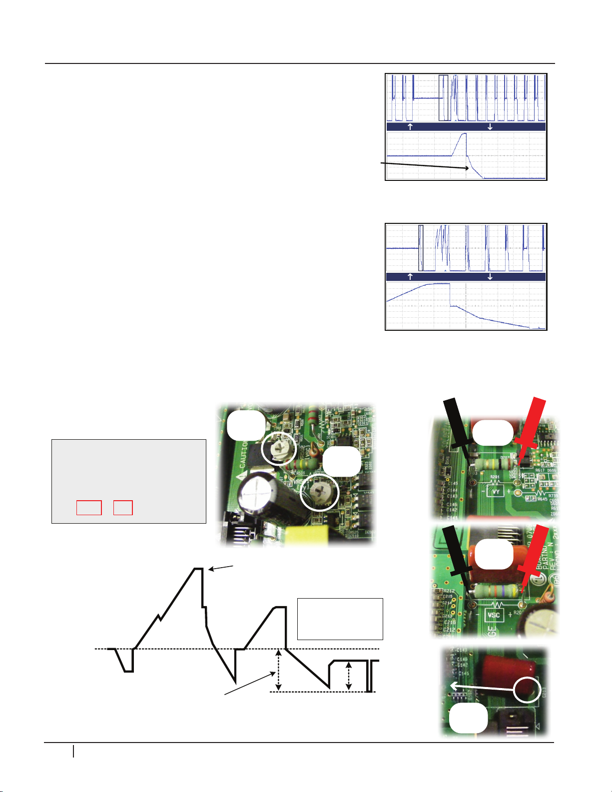
CIRCUIT DESCRIPTIONS
2ms
100us
Area
to be
adjusted
1ms
20us
Area to be
adjusted
expanded
Upper Left
of Y-Drive
Model : PDP50G1####
||||||||||||||||||||||||||||||||||||||||||||||||||||
700
K000G0000000.AKLGGEC
Voltage Setting : DC 5.2V
Va : 65V Vs : 193V
NA / -195 / 135 / NA / 100
VSC
-VY
Model : PDP50G1####
||||||||||||||||||||||||||||||||||||||||||||||||||||
700K000G0000000 .AKLGGEC
Voltage Setting : DC 5.2V
Va : 65V Vs : 193V
NA / -195 / 135 / NA / 100
VSC
-VY
Lower Left
of Y-Drive
R201
-VY TP
R202
VSC TP
VR502
VSC Adj
VR501
-VY Adj
Y Waveform
0V
Sync to this tip
-Vy = -195V
R501
Vsc = 135V
R502
This voltage actually reads
Positive during DC adjustment
Note: These
adjustments are DC
voltage adjustments
-Vy and Vsc DC Adjustments Effects on Y Drive Waveform
Center Left
of Y-Sus
C213
Y-Sus TP
+
-
+
-
At 2ms per/div. the outlined signal for Vsetdn
is now easier to recognize. It is outlined within
the Waveform. At 100uSec per/division, the
waveform to use for Vsetdn is now isolated.
At 1ms per/div. the outlined signal for Vsetdn
is now clearly visible. It is outlined within
the Waveform At 20uSec per/division, the
adjustment for Vsetdn can be made.
vSC AND -vY ADJUSTMENTS
Va/Vs adjustments should already be completed. If VSC is too high or too low, the image
will display some distortion in a quickly changing image.
5
0
P
G
2
0
84 PDP Training - Fall 2008
Page 87
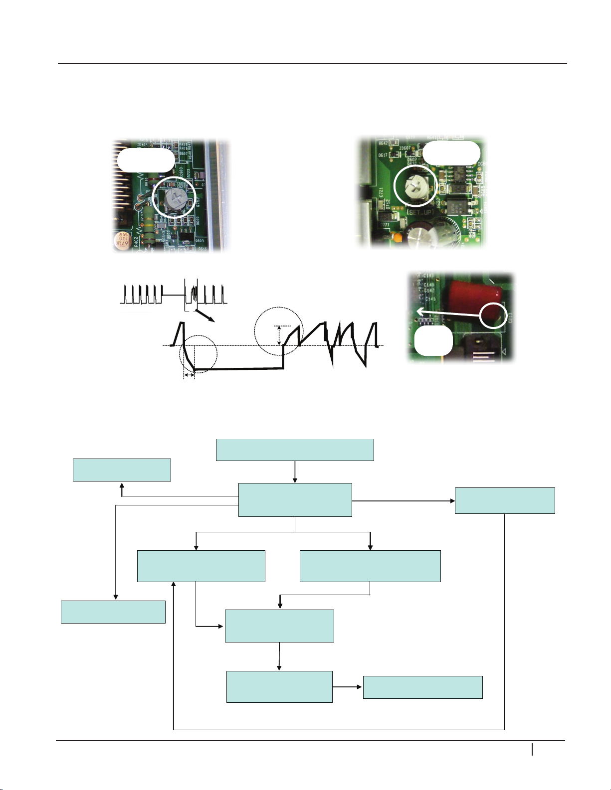
CIRCUIT DESCRIPTIONS
VR601
V-Set Down
C213
Y-Sus TP
Upper Left
of Y-Drive
Upper Right
of Y-Drive
VR602
V-Set Up
50PG20 V-Set-Up/Set-Down Adjustment
1: Vs, Va, Vsc, -Vy adjustments
should already be complete.
150V
+
-
5V
5us
100
-
+
A
B
Y Waveform
0V
Y Set-Up (Ramp)
VR602
Y SET-UP / Y SET-Down Waveform
Y Set-Down (Ramp
Dn) VR601
B) Observe the “Time” Portion of the waveform.
A) Observe
the “Peak”
Portion of
the waveform.
Generates Vsc, -Vy and V Set Up
from Vs by transformer
Control Board
Components generate
Sustain Waveform
Distributes 5V VA VS
Distributes 5V
Logic signals
needed to
generate drive
waveform
Distributes 5V VA
Receive 5V VCC, Va, Vs
from SMPS
Transfer Waveform
to Y Drive Board
Z SUS Board
Left X Board
Display Panel
Power Supply Board - SMPS
FETs amplify Sustain
Waveform
NO IPMs
v-SET UP AND v-SET DOWN ADJUSTMENTS
Va/Vs/Vsc –Vy and ZBias should already been completed.
PANEl WAvEFORM ADJUSTMENT
Y-SUSTAIN DIAGRAM
5
0
P
G
2
0
PDP Training - Fall 2008 85
Page 88
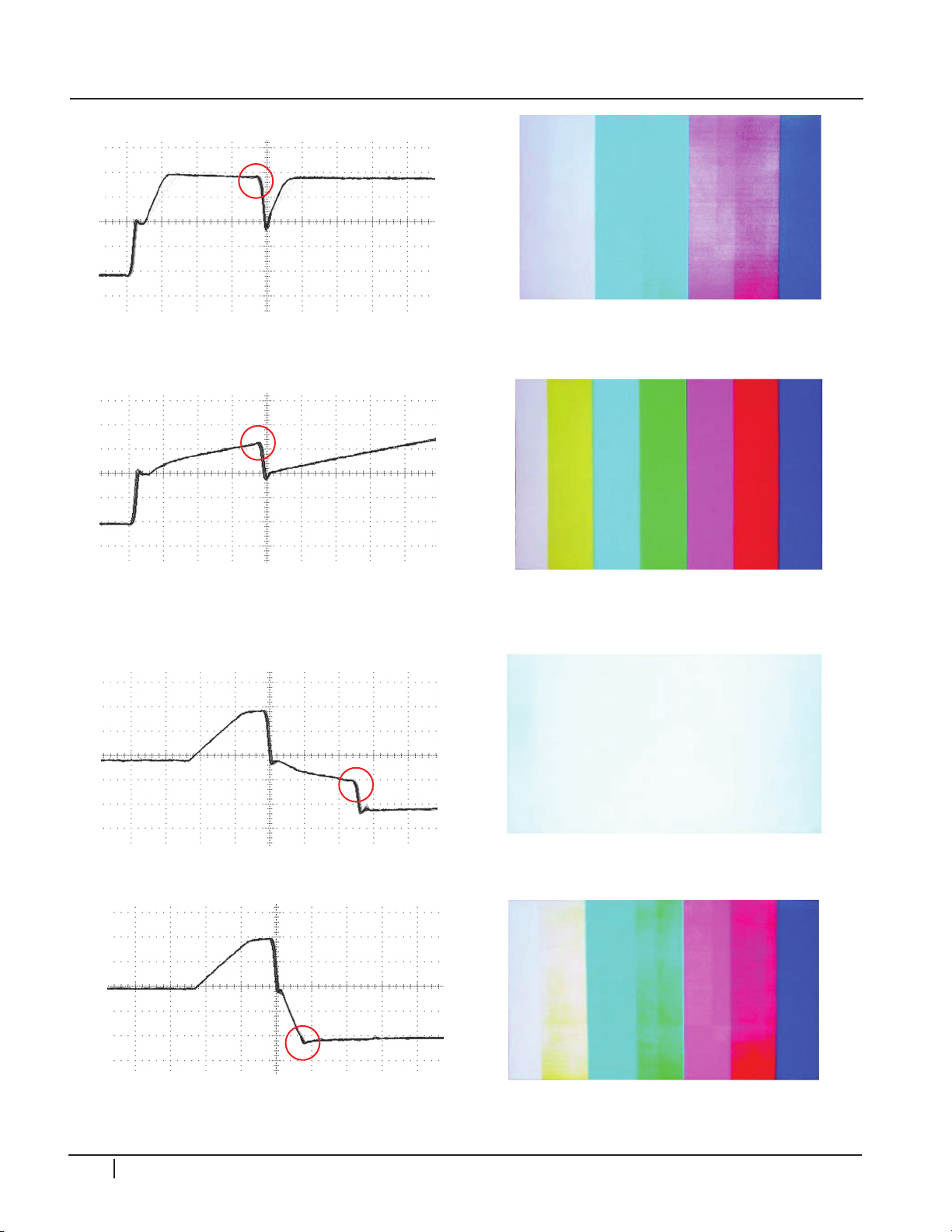
CIRCUIT DESCRIPTIONS
v-SET UP TOO hIGh OR lOW
5
0
V-Set Up Too High
V-Set Up Too Low
v-SET DOWN TOO hIGh OR lOW
The center begins to wash out and arc due to Vset UP
Peeking too late and alters the start of the Vset DN
phase.
Very little alteration to the picture, the wave form
indicates a distorted Vset UP. The peek widens due to
the Vset UP peeking too quickly.
P
G
2
0
V-Set Down Too High
V-Set Down Too Low
86 PDP Training - Fall 2008
All of the center washes out due to increased Vset_DN
time.
Page 89
CIRCUIT DESCRIPTIONS
P102 vOlTAGES
P102 This connector is a little confusing in its labeling. This is a 50 Pin Connector. Pin
1 is inverted on the Control board. It goes 1 (CLK) 2 (STB) 3 (OSC1) 4 (OSC2) 5
(DATA), etc. In other words, there is a ground between each pin. Roughly the first 39
pins are dedicated to Y-Sus. Pins 40-44 are 5V B+ to the Control board. Pins 45-50 are
not used.
P102 “Y-Sus” to P111 “Control”
Pin Label Stby Run Resistance Pin Label Stby Run Resistance
1 CLK 0V 3.2V 2.87V 11 SET_DN 0V 0.2V 2.87V
2 STB 0V 0.76V 2.87V 12 PASS_TOP 0V 0.2V 2.87V
3 OSC1 0V 0V 2.87V 13 DELTA_VY 0V 0.16V 2.87V
4 OSC2 0V 3V 2.87V 14 DET_LEVEL 0V 0V 2.87V
5 D ATA 0V 0.6V 2.87V 15 SLOPE_KEY 0V 0V 2.87V
6 SUS_DN 0V 0V 2.87V 16 SET_UP 0V 1.9V 2.87V
7 SUS_UP 0V 2V 2.87V 17 SET_DN 0V 1.4V 2.87V
8 ER_DN 0V 1.2V 2.87V 18 X_ER 0V 2.9V 2.87V
9 ER_UP 0V 2V 2.87V 19 Y_ENABLE 0V 0.6V 2.87V
10 SET_UP 0V 0.26V 2.87V
P210 “Y-Sus” to P242 “X-Drive Center”
P209 “Y-Sus” to P801 “Power Supply”
Pin Label Stby Run Resistance
Pin Label Stby Run Resistance
1 Va_C 0V 65V OL
1 Vs 0V 192V OL
2 Va_C 0V 65V OL
2 Vs 0V 192V OL
3 VPP_Out_XR 0V 62.4V OL
3 nc nc nc nc
4 VPP_Out_XR 0V 62.4V OL
4 Gnd Gnd Gnd Gnd
5 VPP_Out_XL 0V 62.3V OL
5 Gnd Gnd Gnd Gnd
6 VPP_Out_XL 0V 62.3V OL
6 Va 0V 65V OL
7 VPP_Out 0V 63.3V OL
7 Va 0V 65V OL
8 VPP_Out 0V 63.3V OL
8 Gnd Gnd Gnd Gnd
9 Gnd Gnd Gnd Gnd
9 M5V 0V 5V 0.897V
10 Gnd Gnd Gnd Gnd
10 M5V 0V 5V 0.897V
11 +15V 0V 15.9V 0.95V
5
0
P
G
2
0
12 +15V 0V 15.9V 0.95V
PDP Training - Fall 2008 87
Page 90
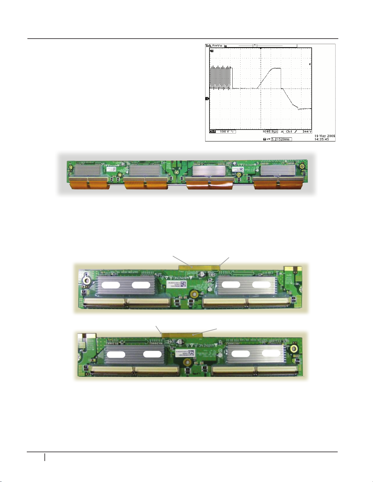
CIRCUIT DESCRIPTIONS
Logic Signals From the Y-Sus
P100
+5V
+5V
Logic Signals From the Y-Drive
P200
P204
IC203
IC202IC201
IC140
IC130
IC120
IC110
U
P
P
E
R
L
O
W
E
R
Y-DRIVE
Y-Drive board works as a path supplying the
Sustain and Reset waveforms which are made
in the Y-Sustain and sent to the Panel through
Scan Driver IC’s. The Y-Drive boards supply a
waveform which selects the horizontal electrodes
sequentially. 50PG20 uses 8 DRIVER ICs on 2
boards (TOP, BOTTOM: 4 each).
Y-DRIvE ID
5
0
P
G
2
0
5 Volts and Logic Signals from Y-Sus board are supplied to the top drive board on
connector P100. 5 volts input (shown below). Also they enter the bottom Y-Drive board
at P200.
88 PDP Training - Fall 2008
Page 91
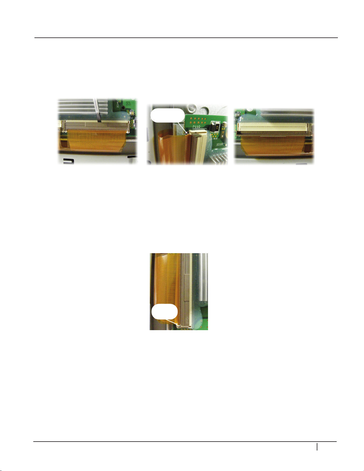
CIRCUIT DESCRIPTIONS
Tab
Exposed
Figure 1 Figure 2 Figure 3
Be sure tab
is released
Y-DRIvE RIbbON CAblE REMOvAl
To remove the ribbon cable from the connector first carefully lift the Locking Tab from the
back and tilt it forward (lift from the outside edge as shown in Fig1). Lift up the entire
ribbon cable gently to release the tabs on each end. Gently slide the ribbon cable free
from the connector.
INCORRECTlY SEATED RIbbON CAblE
The ribbon cable below is clearly improperly seated into the connector. You can tell by
observing the linearity. Note the cable is crooked. In this case the tab on the ribbon
cable was improperly seated at the bottom. This can cause bars, lines, intermittent lines
abnormalities in the picture. Remove the ribbon cable and re-seat it correctly.
5
0
P
G
2
0
PDP Training - Fall 2008 89
Page 92
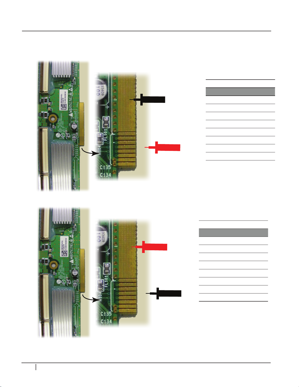
CIRCUIT DESCRIPTIONS
Y-Drive Upper Contacts
Data
DC1
DC2
LE
CLK
Data-Out
+5V
+5V
+
-
Y-Drive Upper Contacts
Data
DC1
DC2
LE
CLK
Data-Out
+5V
+5V
+
-
UPPER Y-DRIvE DIODE TEST
Using the “Diode Test” on the DVM, check the pins for shorts or abnormal loads.
Diode Test
Test Point Reading
Data Open
DC1 Open
DC2 Open
LE Open
CLK Open
Data-Out Open
+5V Open
+5V Open
5
0
P
G
2
0
Diode Test
Test Point Reading
Data .78 V
DC1 .63 V
DC2 .63 V
LE .63 V
CLK .63 V
Data-Out .73V
+5V .53V
+5V .53V
90 PDP Training - Fall 2008
Page 93
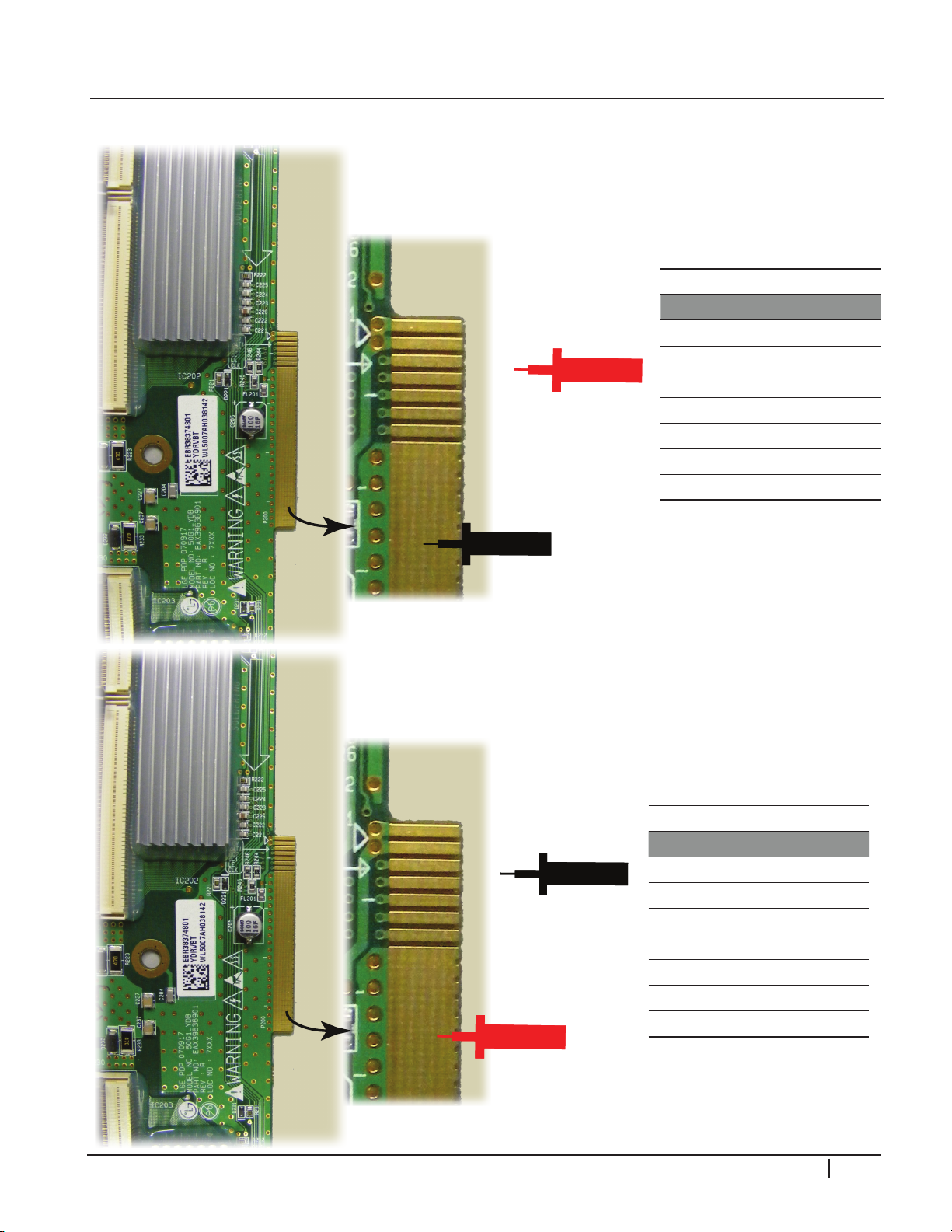
Y-Drive Lower Contacts
+5V
+5V
Data
DC2
DC1
LE
CLK
+
-
Y-Drive Lower Contacts
+5V
+5V
Data
DC2
DC1
LE
CLK
+
-
UPPER Y-DRIvE DIODE TEST
CIRCUIT DESCRIPTIONS
Diode Test
Test Point Reading
+5V Open
+5V Open
Data Open
DC2 Open
DC1 Open
LE Open
CLK Open
5
0
Diode Test
Test Point Reading
+5V .52 V
+5V .52 V
Data .78 V
DC2 .61 V
DC1 .62 V
LE .62 V
CLK .62 V
P
G
2
0
PDP Training - Fall 2008 91
Page 94
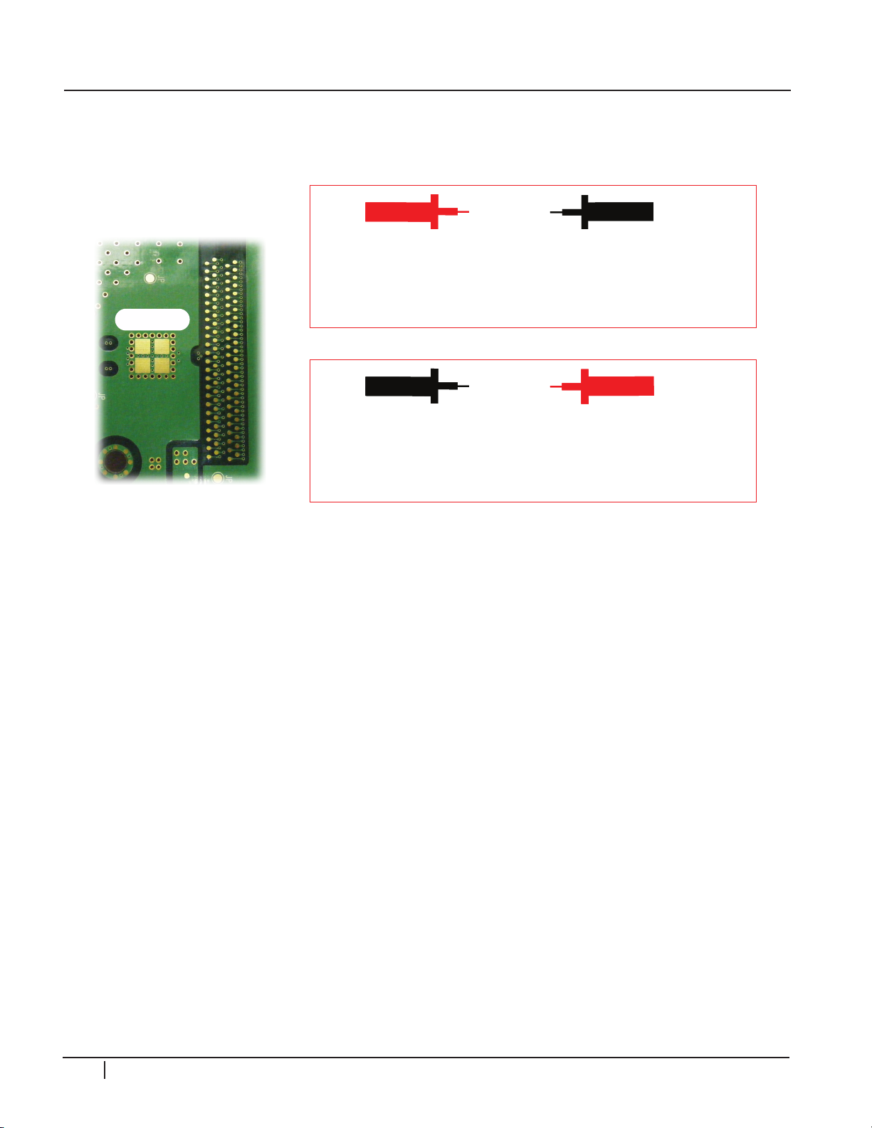
CIRCUIT DESCRIPTIONS
Buer IC
Output Lugs
RED LEAD ON
BUFFER IC
BLACK LEAD ON “ANY”
OUTPUT LUG.
READING 0.73 V
BLACK LEAD ON
BUFFER IC
RED LEAD ON “ANY”
OUTPUT LUG.
READING “OPEN”
Indicated by Red outline
Indicated by Red outline
bUFFER IC ChECk
Using the “Diode Test” on the DVM, check the pins for shorts or abnormal loads. Any of
the output lugs can be tested. Look for shorts indicating a defective Buffer IC.
+
-
-
+
5
0
P
G
2
0
92 PDP Training - Fall 2008
Page 95
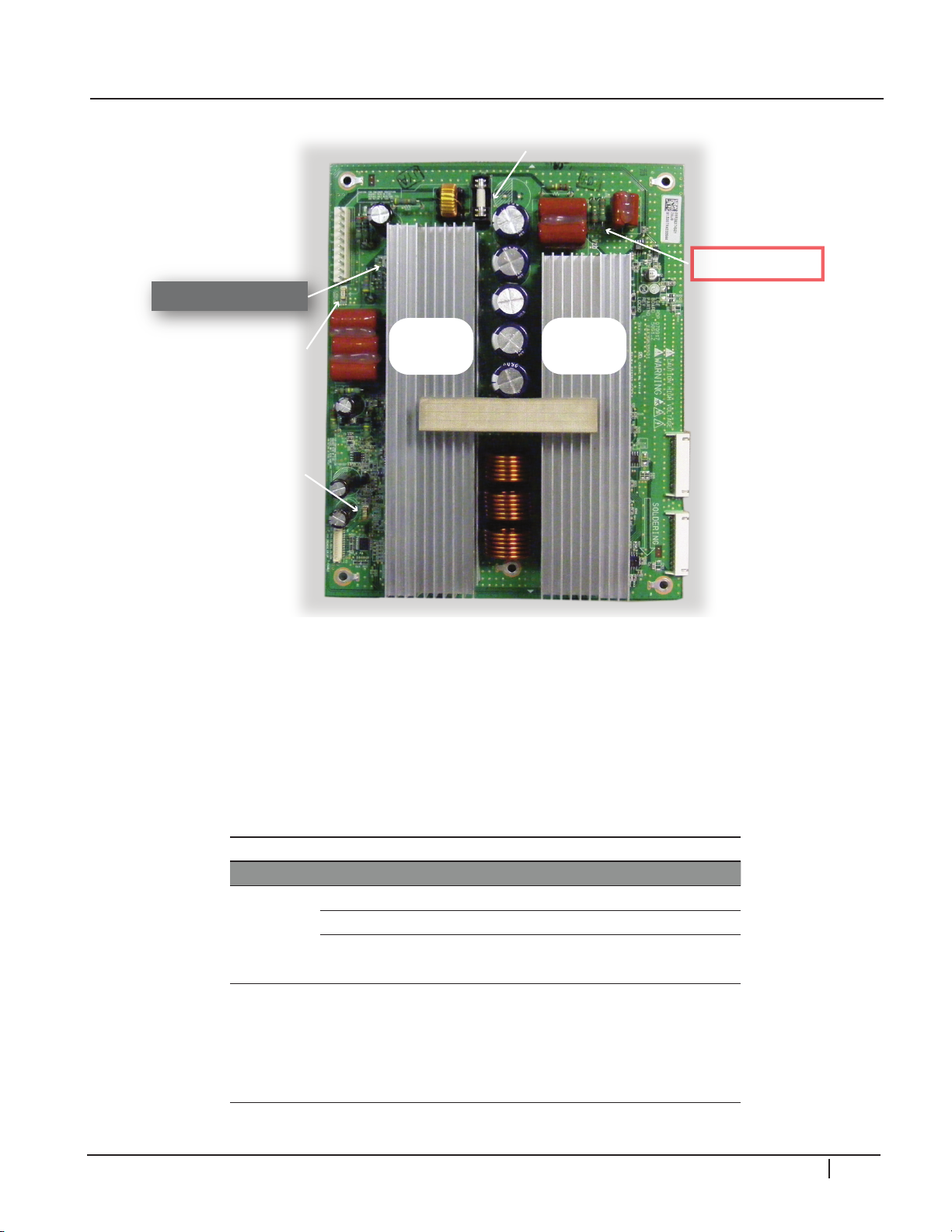
Z-SUS BOARD
P4
FS2 (5V)
125V 10A
P5
FS3 (16V)
125V 1.5A
P2
Logic Signals
From Control Board
Discrete
Components
(No IPMs)
VR8 Z-Bias Control
Z-Bias Test Point
P3
From SMPS
Discrete
Components
(No IPMs)
To Z-Sus
FS1 (Vs)
250V 4A
CIRCUIT DESCRIPTIONS
Order both Z-Sus and Z-Sub board when either board needs to be replaced. This assures
each connector is gender match. On original boards, P4 and P5 are male connectors. On
replacement boards they will be female. Z-Bias is a “DC” adjustment. The effects of this
adjustment can be observed on the scope looking at the Z-Sus output.
Z-Sus Input Voltages
Board Voltage Description
VS VS is input supplied to the driver IC circuit.
Y-Sus
DEveloped
on Z-Sus
VA VA inputs are supplied to the driver IC circuit.
5V VCC
Z-Bias
5V is used to Bias the circuits on the Z-Sus
board.
Z Bias Voltage is used to Bias the output circuits
driving the Sustain and Erase
Pulses, removing previous images from the
PDP. Z-bias is measured from the
Vzb TP on the Z -SUS board and adjusted by
VZB Adj.
5
0
P
G
2
0
PDP Training - Fall 2008 93
Page 96
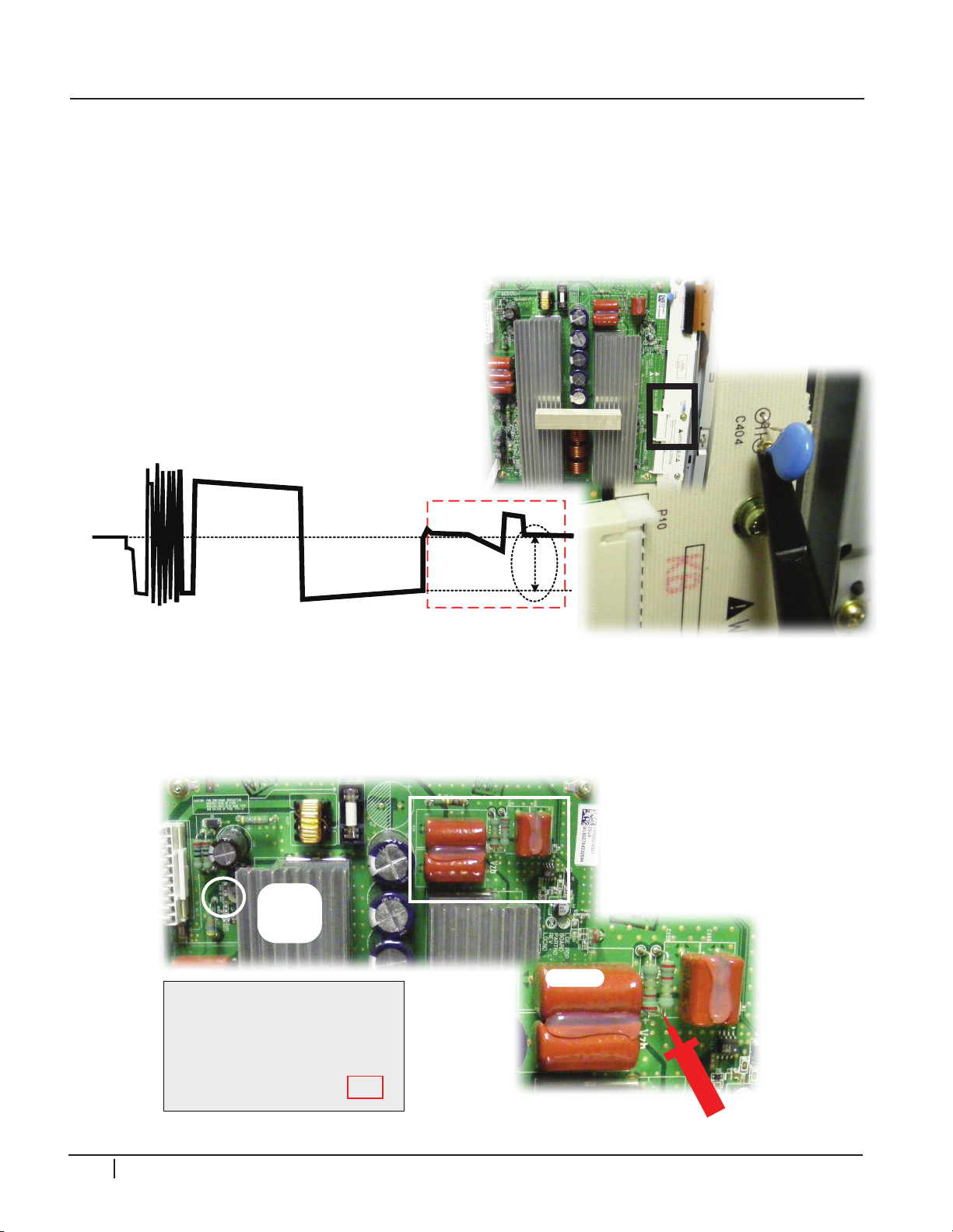
CIRCUIT DESCRIPTIONS
Center Right
of Z-Sus
Vzb voltage
+
-
1V
100V
0 V
Z Bias (Z-Sus Waveform)
(Vzb) Z Bias VR8
Note This adjustment is a DC voltage adjustment
Attach probe
to upper leg
of C404
VZB TP
Model : PDP50G1####
||||||||||||||||||||||||||||||||||||||||||||||||||||
700
K000G0000000.AKLGGEC
Voltage Setting : DC 5.2V
Va : 65V Vs : 193V
NA / -195 / 135 / NA / 100
Model : PDP50G1####
||||||||||||||||||||||||||||||||||||||||||||||||||||
700K000G0000000 .AKLGGEC
Voltage Setting : DC 5.2V
Va : 65V Vs : 193V
NA / -195 / 135 / NA / 100
Z-Bias
VR8
Z-Bias
Control
+
Z-SUS WAvEFORM
Provides the Sustain Pulse and Erase Pulse for generating Sustain discharge in the panel
by receiving Logic signals from the Control board. This waveform is supplied to the panel
through FPC (Flexible Printed Circuit (Z). Z-Bias is a “DC” adjustment. The effects of this
adjustment can be observed on the scope looking at the Z-Sus output.
5
Z-SUS ADJUST
Z-Bias Adjust VR 8, measurement from VZB test point to chassis ground. Adjust to the
level indicated on the voltage sticker on the upper Left-Hand side of the panel.
0
P
G
2
0
94 PDP Training - Fall 2008
Page 97
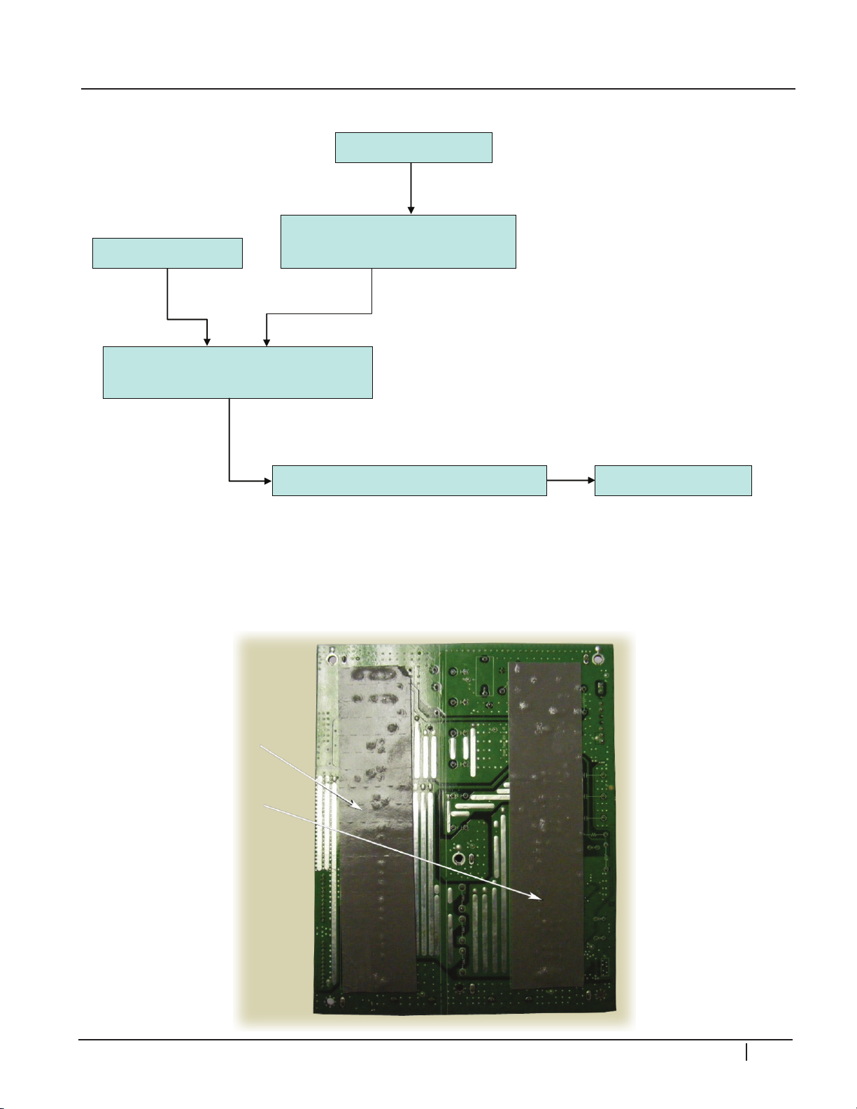
Z-SUS blOCk DIAGRAM
Drive Circuit generates
sustain waveforms
Distributes Logic Signals
Distributes 5V VCC, VA, VS
FET Makes Drive waveform
Display Panel
Via FPC (flexible printed circuit )
Control Board
Receive 5V VCC, VA, VS
Y SUS Board
NO IPMs
CIRCUIT DESCRIPTIONS
Z-SUS NOISE DAMPING PADS
Make sure the replacement boards come with the noise reducing pads. If they do not,
contact parts about sending the two pads.
5
0
P
G
2
0
PDP Training - Fall 2008 95
Page 98
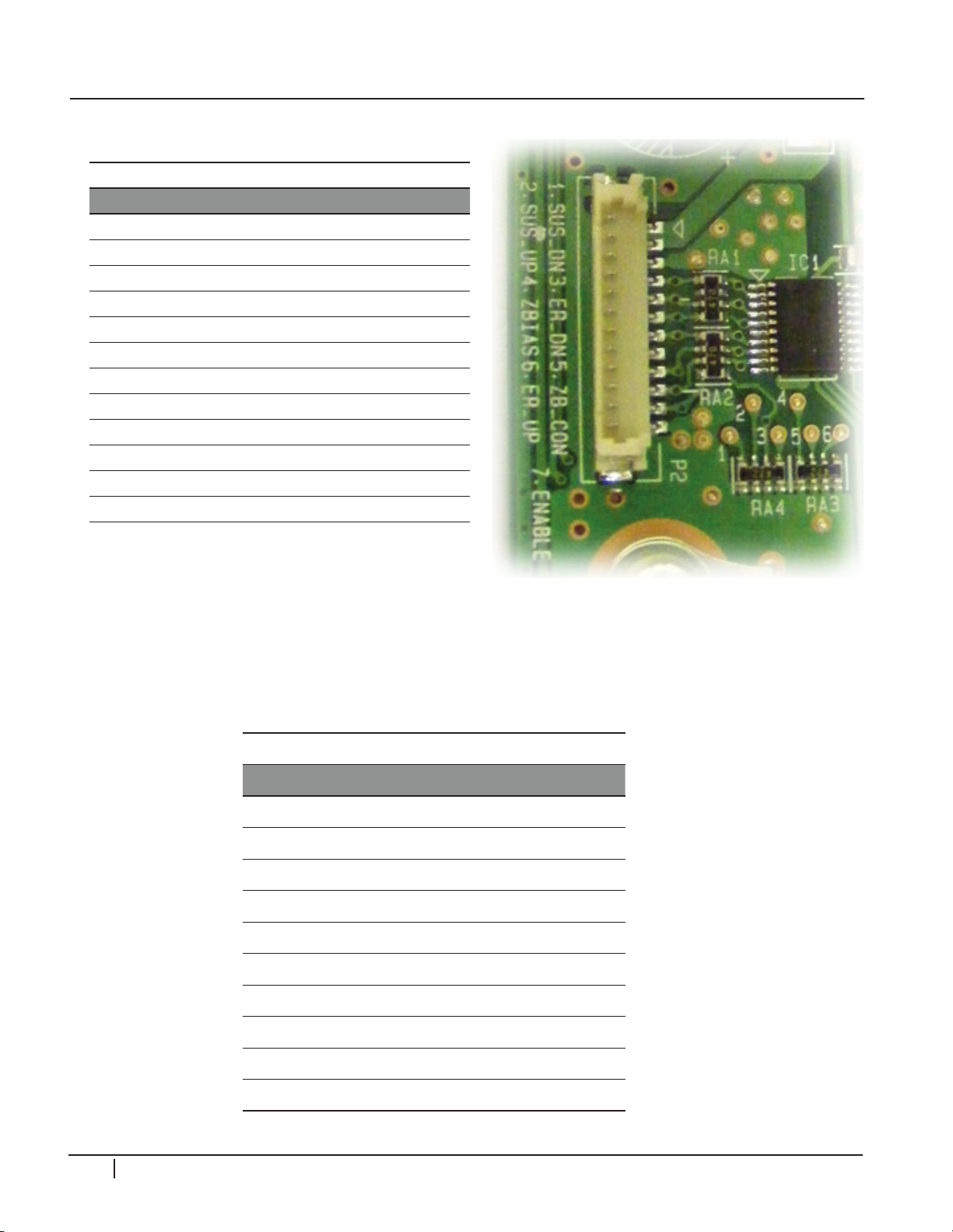
CIRCUIT DESCRIPTIONS
P2 “Z-Sus” to P163 “Control”
Pin Label Stby Run Resistance
1 SUS-DN 0V 16V 2.69V
2 SUS-UP 0V 16V 2.69V
3 ER-DN Gnd Gnd Gnd
4 ZBIAS 0V 0.48V 2.85V
5 ZB-CON 0V 0.27V 2.85V
6 ER-UP 0V 0.1V 2.85V
7 ENABLE 0V 0.06V 2.85V
8 none Gnd Gnd Gnd
9 none 0V 0V 2.85V
10 none 0V 1.93V 2.85V
11 none 0V 2.66V 0.66V
12 none Gnd Gnd Gnd
5
0
P
G
2
0
Note: These labels are actually backwards. Pin 1 is actually Pin 12. This is because the pin
numbers are inverted from the Controlboard.
P3 “Z-Sus” to P802 “Power Supply”
Pin Label Stby Run Resistance
1 Vs 0V 192V OL
2 Vs 0V 192V OL
3 nc nc nc nc
4 Gnd Gnd Gnd Gnd
5 Gnd 0V 0V Gnd
6 Va 0V 65V OL
7 Va 0V 65V OL
8 Gnd Gnd Gnd Gnd
9 M5V 0V 5V 1.3V
96 PDP Training - Fall 2008
10 M5V 0V 5V 1.3V
Page 99
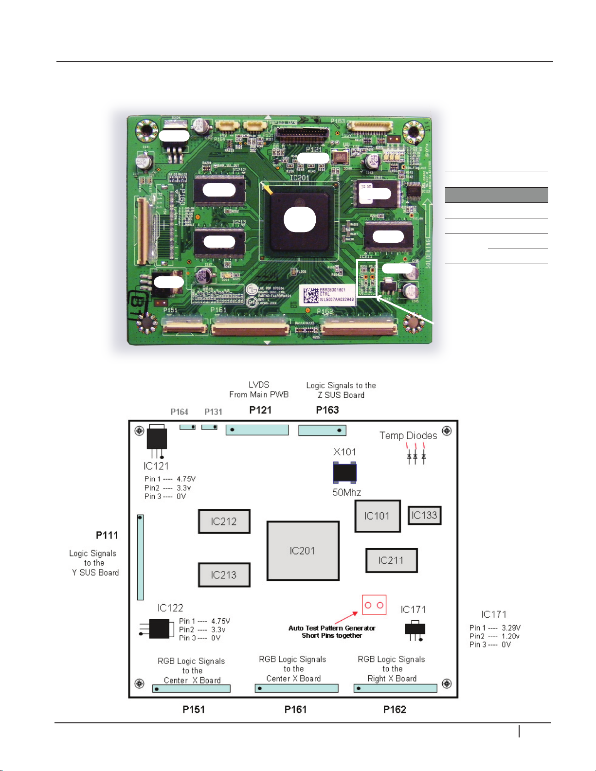
CONTROL BOARD
IC211
P121
LVDS
IC121
IC201
MCM
IC212
IC213
IC122
IC171
Auto Generated
Test Pattern
IC101
P164 P131
(No Connection)
P163
To Z-Sus
Temperature
LEDs
X101
P111
To Y-Sus
(Pins Inverted
on Y-Sus)
P151
To X-Drive Center
P161
To X-Drive Center
P162
To X-Drive Right
CIRCUIT DESCRIPTIONS
Control board Inputs
Board Input
Main LVDS
Y-Sus 5V VCC
Control
1.8V
3.3V
5
0
P
G
2
0
PDP Training - Fall 2008 97
Page 100
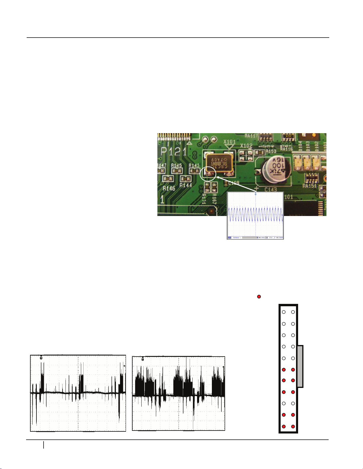
CIRCUIT DESCRIPTIONS
50Mhz
500mV 40ns
1
3
5
7
9
11
13
15
17
19
21
2
4
6
8
10
12
14
16
18
20
22
Connector P302 Configuration
- indicates signal pins.
Menu (OSD) Off
Menu (OSD) ON
CONTROl bOARD QUICk TEST
With all board connectors disconnected, Jump 5V from the Power Supply to IC121 pin.
If the Temp LED lights, the board is ok. When the Television has a problem related to
shutdown caused by the main board or no picture, it can be checked by the following.
Disconnect the Main board from all connectors. Apply AC power. Since P803 is not
connected, the set will come on. Short the two pins on the Auto Test Pattern lands. If
there is a picture of cycling colors, the Y-SUS, Y-Drive, Z-SUS, Power Supply, Control
boards, and panel are all ok. Check FL111 and FL112 to be sure they are ok.
CRYSTAl ClOCk TEST
Check the output of the oscillator
package. The frequency of the
sine wave is 50 MHZ. Missing this
clock signal can halt operation of
the unit.
lvDS SIGNAlS
Video signals from the Main board
to the Control board are referred to
as Low Voltage Differential Signals
5
0
P
G
2
0
or LVDS. Their presence can be confirmed with an oscilloscope by
monitoring the LVDS signals with no input signal selected while
pressing the Menu Button with the remote control or keypad. Loss
of these signals would confirm the failure is on the Main board.
Use only Component Input. Select by remote by guess since
there’s no video. Toggle between menu on/off to see a difference
in waveform. Below are examples of Normal Signals measured at
200mv/cm at 5us/cm.
98 PDP Training - Fall 2008
 Loading...