

Page 1

Internal Use Only
North/Latin America http://aic.lgservice.com
Europe/Africa http://eic.lgservice.com
Asia/Oceania http://biz.lgservice.com
LCD TV
SERVICE MANUAL
CHASSIS : LC12C
MODEL : 42LW6500 42LW6500-CA
47LW6500
55LW6500
65LW6500
CAUTION
BEFORE SERVICING THE CHASSIS,
READ THE SAFETY PRECAUTIONS IN THIS MANUAL.
47LW6500-CA
55LW6500-CA
65LW6500-CA
Printed in ChinaP/NO : MFL66984501 (1104-REV00)
Page 2

CONTENTS
CONTENTS .............................................................................................. 2
SAFETY PRECAUTIONS ......................................................................... 3
SPECIFICATION ....................................................................................... 6
ADJUSTMENT INSTRUCTION ..............................................................59
EXPLODED VIEW ..................................................................................90
SVC. SHEET ...............................................................................................
- 2 -
Page 3
- 3 -
SAFETY PRECAUTIONS
Many electrical and mechanical parts in this chassis have special safety-related characteristics. These parts are identified by in the
Schematic Diagram and Exploded View.
It is essential that these special safety parts should be replaced with the same components as recommended in this manual to prevent
Shock, Fire, or other Hazards.
Do not modify the original design without permission of manufacturer.
General Guidance
An isolation Transformer should always be used during the
servicing of a receiver whose chassis is not isolated from the AC
power line. Use a transformer of adequate power rating as this
protects the technician from accidents resulting in personal injury
from electrical shocks.
It will also protect the receiver and it's components from being
damaged by accidental shorts of the circuitry that may be
inadvertently introduced during the service operation.
If any fuse (or Fusible Resistor) in this TV receiver is blown,
replace it with the specified.
When replacing a high wattage resistor (Oxide Metal Film Resistor,
over 1W), keep the resistor 10mm away from PCB.
Keep wires away from high voltage or high temperature parts.
Before returning the receiver to the customer,
always perform an AC leakage current check on the exposed
metallic parts of the cabinet, such as antennas, terminals, etc., to
be sure the set is safe to operate without damage of electrical
shock.
Leakage Current Cold Check(Antenna Cold Check)
With the instrument AC plug removed from AC source, connect an
electrical jumper across the two AC plug prongs. Place the AC
switch in the on position, connect one lead of ohm-meter to the AC
plug prongs tied together and touch other ohm-meter lead in turn to
each exposed metallic parts such as antenna terminals, phone
jacks, etc.
If the exposed metallic part has a return path to the chassis, the
measured resistance should be between 1MΩ and 5.2MΩ.
When the exposed metal has no return path to the chassis the
reading must be infinite.
An other abnormality exists that must be corrected before the
receiver is returned to the customer.
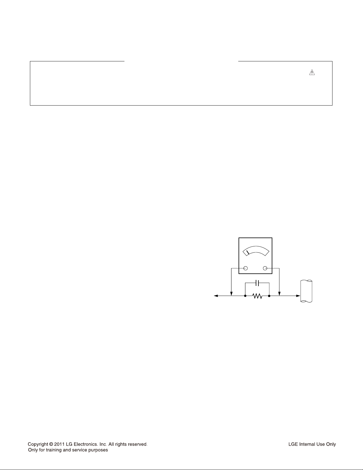
Leakage Current Hot Check (See below Figure)
Plug the AC cord directly into the AC outlet.
Do not use a line Isolation Transformer during this check.
Connect 1.5K/10watt resistor in parallel with a 0.15uF capacitor
between a known good earth ground (Water Pipe, Conduit, etc.)
and the exposed metallic parts.
Measure the AC voltage across the resistor using AC voltmeter
with 1000 ohms/volt or more sensitivity.
Reverse plug the AC cord into the AC outlet and repeat AC voltage
measurements for each exposed metallic part. Any voltage
measured must not exceed 0.75 volt RMS which is corresponds to
0.5mA.
In case any measurement is out of the limits specified, there is
possibility of shock hazard and the set must be checked and
repaired before it is returned to the customer.
Leakage Current Hot Check circuit
1.5 Kohm/10W
To Instrument’s
exposed
METALLIC PARTS
Good Earth Ground
such as WATER PIPE,
CONDUIT etc.
AC Volt-meter
IMPORTANT SAFETY NOTICE
0.15uF
Page 4

- 4 -
CAUTION: Before servicing receivers covered by this service
manual and its supplements and addenda, read and follow the
SAFETY PRECAUTIONS on page 3 of this publication.
NOTE: If unforeseen circumstances create conflict between the
following servicing precautions and any of the safety precautions on
page 3 of this publication, always follow the safety precautions.
Remember: Safety First.
General Servicing Precautions
1. Always unplug the receiver AC power cord from the AC power
source before;
a. Removing or reinstalling any component, circuit board
module or any other receiver assembly.
b. Disconnecting or reconnecting any receiver electrical plug or
other electrical connection.
c. Connecting a test substitute in parallel with an electrolytic
capacitor in the receiver.
CAUTION: A wrong part substitution or incorrect polarity
installation of electrolytic capacitors may result in an
explosion hazard.
2. Test high voltage only by measuring it with an appropriate high
voltage meter or other voltage measuring device (DVM,
FETVOM, etc) equipped with a suitable high voltage probe.
Do not test high voltage by "drawing an arc".
3. Do not spray chemicals on or near this receiver or any of its
assemblies.
4. Unless specified otherwise in this service manual, clean
electrical contacts only by applying the following mixture to the
contacts with a pipe cleaner, cotton-tipped stick or comparable
non-abrasive applicator; 10% (by volume) Acetone and 90% (by
volume) isopropyl alcohol (90%-99% strength)
CAUTION: This is a flammable mixture.
Unless specified otherwise in this service manual, lubrication of
contacts in not required.
5. Do not defeat any plug/socket B+ voltage interlocks with which
receivers covered by this service manual might be equipped.
6. Do not apply AC power to this instrument and/or any of its
electrical assemblies unless all solid-state device heat sinks are
correctly installed.
7. Always connect the test receiver ground lead to the receiver
chassis ground before connecting the test receiver positive
lead.
Always remove the test receiver ground lead last.
8. Use with this receiver only the test fixtures specified in this
service manual.
CAUTION: Do not connect the test fixture ground strap to any
heat sink in this receiver.
Electrostatically Sensitive (ES) Devices
Some semiconductor (solid-state) devices can be damaged easily
by static electricity. Such components commonly are called
Electrostatically Sensitive (ES) Devices. Examples of typical ES
devices are integrated circuits and some field-effect transistors and
semiconductor "chip" components. The following techniques
should be used to help reduce the incidence of component
damage caused by static by static electricity.
1. Immediately before handling any semiconductor component or
semiconductor-equipped assembly, drain off any electrostatic
charge on your body by touching a known earth ground.
Alternatively, obtain and wear a commercially available
discharging wrist strap device, which should be removed to
prevent potential shock reasons prior to applying power to the
unit under test.
2. After removing an electrical assembly equipped with ES
devices, place the assembly on a conductive surface such as
aluminum foil, to prevent electrostatic charge buildup or
exposure of the assembly.
3. Use only a grounded-tip soldering iron to solder or unsolder ES
devices.
4. Use only an anti-static type solder removal device. Some solder
removal devices not classified as "anti-static" can generate
electrical charges sufficient to damage ES devices.
5. Do not use freon-propelled chemicals. These can generate
electrical charges sufficient to damage ES devices.
6. Do not remove a replacement ES device from its protective
package until immediately before you are ready to install it.
(Most replacement ES devices are packaged with leads
electrically shorted together by conductive foam, aluminum foil
or comparable conductive material).
7. Immediately before removing the protective material from the
leads of a replacement ES device, touch the protective material
to the chassis or circuit assembly into which the device will be
installed.
CAUTION: Be sure no power is applied to the chassis or circuit,
and observe all other safety precautions.
8. Minimize bodily motions when handling unpackaged
replacement ES devices. (Otherwise harmless motion such as
the brushing together of your clothes fabric or the lifting of your
foot from a carpeted floor can generate static electricity
sufficient to damage an ES device.)
General Soldering Guidelines
1. Use a grounded-tip, low-wattage soldering iron and appropriate
tip size and shape that will maintain tip temperature within the
range or 500°F to 600°F.
2. Use an appropriate gauge of RMA resin-core solder composed
of 60 parts tin/40 parts lead.
3. Keep the soldering iron tip clean and well tinned.
4. Thoroughly clean the surfaces to be soldered. Use a mall wirebristle (0.5 inch, or 1.25cm) brush with a metal handle.
Do not use freon-propelled spray-on cleaners.
5. Use the following unsoldering technique
a. Allow the soldering iron tip to reach normal temperature.
(500°F to 600°F)
b. Heat the component lead until the solder melts.
c. Quickly draw the melted solder with an anti-static, suction-
type solder removal device or with solder braid.
CAUTION: Work quickly to avoid overheating the circuit
board printed foil.
6. Use the following soldering technique.
a. Allow the soldering iron tip to reach a normal temperature
(500°F to 600°F)
b. First, hold the soldering iron tip and solder the strand against
the component lead until the solder melts.
c. Quickly move the soldering iron tip to the junction of the
component lead and the printed circuit foil, and hold it there
only until the solder flows onto and around both the
component lead and the foil.
CAUTION: Work quickly to avoid overheating the circuit
board printed foil.
d. Closely inspect the solder area and remove any excess or
splashed solder with a small wire-bristle brush.
SERVICING PRECAUTIONS
Page 5

- 5 -
IC Remove/Replacement
Some chassis circuit boards have slotted holes (oblong) through
which the IC leads are inserted and then bent flat against the
circuit foil. When holes are the slotted type, the following technique
should be used to remove and replace the IC. When working with
boards using the familiar round hole, use the standard technique
as outlined in paragraphs 5 and 6 above.
Removal
1. Desolder and straighten each IC lead in one operation by gently
prying up on the lead with the soldering iron tip as the solder
melts.
2. Draw away the melted solder with an anti-static suction-type
solder removal device (or with solder braid) before removing the
IC.
Replacement
1. Carefully insert the replacement IC in the circuit board.
2. Carefully bend each IC lead against the circuit foil pad and
solder it.
3. Clean the soldered areas with a small wire-bristle brush.
(It is not necessary to reapply acrylic coating to the areas).
"Small-Signal" Discrete Transistor
Removal/Replacement
1. Remove the defective transistor by clipping its leads as close as
possible to the component body.
2. Bend into a "U" shape the end of each of three leads remaining
on the circuit board.
3. Bend into a "U" shape the replacement transistor leads.
4. Connect the replacement transistor leads to the corresponding
leads extending from the circuit board and crimp the "U" with
long nose pliers to insure metal to metal contact then solder
each connection.
Power Output, Transistor Device
Removal/Replacement
1. Heat and remove all solder from around the transistor leads.
2. Remove the heat sink mounting screw (if so equipped).
3. Carefully remove the transistor from the heat sink of the circuit
board.
4. Insert new transistor in the circuit board.
5. Solder each transistor lead, and clip off excess lead.
6. Replace heat sink.
Diode Removal/Replacement
1. Remove defective diode by clipping its leads as close as
possible to diode body.
2. Bend the two remaining leads perpendicular y to the circuit
board.
3. Observing diode polarity, wrap each lead of the new diode
around the corresponding lead on the circuit board.
4. Securely crimp each connection and solder it.
5. Inspect (on the circuit board copper side) the solder joints of
the two "original" leads. If they are not shiny, reheat them and if
necessary, apply additional solder.
Fuse and Conventional Resistor
Removal/Replacement
1. Clip each fuse or resistor lead at top of the circuit board hollow
stake.
2. Securely crimp the leads of replacement component around
notch at stake top.
3. Solder the connections.
CAUTION: Maintain original spacing between the replaced
component and adjacent components and the circuit board to
prevent excessive component temperatures.
Circuit Board Foil Repair
Excessive heat applied to the copper foil of any printed circuit
board will weaken the adhesive that bonds the foil to the circuit
board causing the foil to separate from or "lift-off" the board. The
following guidelines and procedures should be followed whenever
this condition is encountered.
At IC Connections
To repair a defective copper pattern at IC connections use the
following procedure to install a jumper wire on the copper pattern
side of the circuit board. (Use this technique only on IC
connections).
1. Carefully remove the damaged copper pattern with a sharp
knife. (Remove only as much copper as absolutely necessary).
2. carefully scratch away the solder resist and acrylic coating (if
used) from the end of the remaining copper pattern.
3. Bend a small "U" in one end of a small gauge jumper wire and
carefully crimp it around the IC pin. Solder the IC connection.
4. Route the jumper wire along the path of the out-away copper
pattern and let it overlap the previously scraped end of the good
copper pattern. Solder the overlapped area and clip off any
excess jumper wire.
At Other Connections
Use the following technique to repair the defective copper pattern
at connections other than IC Pins. This technique involves the
installation of a jumper wire on the component side of the circuit
board.
1. Remove the defective copper pattern with a sharp knife.
Remove at least 1/4 inch of copper, to ensure that a hazardous
condition will not exist if the jumper wire opens.
2. Trace along the copper pattern from both sides of the pattern
break and locate the nearest component that is directly
connected to the affected copper pattern.
3. Connect insulated 20-gauge jumper wire from the lead of the
nearest component on one side of the pattern break to the lead
of the nearest component on the other side.
Carefully crimp and solder the connections.
CAUTION: Be sure the insulated jumper wire is dressed so the
it does not touch components or sharp edges.
Page 6
LGE Display Division
Product Specification
LC12C Product Specification
LC12C
LG 전자
LCD TV Research Department 3
LG ELECTRONICS Inc.
GL1 Group
Page 7
LGE Display Division
LC12C Product Specification
- Contents -
1. Application range.
2. Specification
3. Test Method
4. Electrical Specification
5. Feature and Function
6. Safety and Regulation
7. Video
8. Digital Receiver (DTMB)
9. Digital Receiver (DVB-C)
10. Chroma & Brightness
11. Audio
12. Power
13. Standard Level For Input Signal(Video, Audio, Y/C, Component, RGB)
)
, P
14. Component Video Input (Y, P
B
R
15. RGB Input ( PC )
16. HDMI Input
17. 3D Mode – HDMI & USB
18. RGB/HV Control Signal In/Out Spec(D-sub15 pin Cable )
19. USB Input
20. Magic Remocon
21. WiFi
22. Screen Size(over scan spec)
23. The others
LG 전자
Page 8

LGE Display Division
LC12C Product Specification
24. Reliability
25. LED Control
26. SET factoring condition
27. Accessories & Mechanical Spec.
28. EEI
LG 전자
Page 9
LGE Display Division
LC12C Product Specification
1. Application range.
This spec sheet is applied to the LCD TV used LC12C chassis.
Chassis Basic Model Name Market Place Brand Remarks
LC12C 42/47/55LW6500-CA CHINA,HONG KONG (PAL/DTMB Market) LG
2. Specification
Each part is tested as below without special appointment.`
2.1 Temperature : 25±5℃ (77±9℉), CST : 40±5℃
2.2 Relative Humidity : 65±10%
2.3 Power Voltage : Standard input voltage (100~240V@ 50/60Hz)
Standard Voltage of each product is marked by models
2.4 Specification and performance of each parts are followed each drawing and specification by part number in accordance with BOM .
2.5 The receiver must be operated for about5 minutes prior to the adjustment
LG 전자
Page 10
LGE Display Division
3. Test method
3.1 Performance : LGE TV test method followed.
3.2 Demanded other specification
Safety : CE, IEC specification
EMC : CE, IEC
42/47/55LW6500-CA
Model Market Appliance Remarks
CHINA,HONG KONG
(PAL/DTMB Market)
LC12C Product Specification
Safety : IEC/EN60065
EMI : EN55013
EMS : EN55020
LG 전자
Page 11
LGE Display Division
LC12C Product Specification
4. Electrical Specification
4.1 Module Specification
4.1.1 General Specification
No Item Specification Measurement Result Remark
1 Display Screen Device 42,47,55 Wide Color Display Module LCD
2 Aspect Ratio 16:9
LC420EUF-SDF1 42LW6500-CA
3 LCD Module
4 Operating Environment
5 Storage Environment
6 Input Voltage AC100 ~ 240V, 50/60Hz
Power Consumption
Outline Dimension
7
Pixel Pitch
Back Light
Color depth
Surface treatment
LC470EUF-SDF1 47LW6500-CA
LC550EUF-SDF1 55LW6500-CA
Temp. : 0 ~ 50 deg
Humidity : 20 ~ 90 %
Temp. : -20 ~ 60 deg
Humidity : 10 ~ 90 %
42” LGD Typ : 90.5W (Total.)
47” LGD Typ : 101.1W (Total)
55” LGD Typ : 108.5W (Total.)
42” LGD
47” LGD
55” LGD
42” LGD
47” LGD
55” LGD
42” LGD
47” LGD
55” LGD
968.4(H) x 564.0(V) x 10.8(B) / 22.9mm(D)
1078.6(H) x 626.0(V) x 10.8(B) / 22.9mm (D)
1209.6(H) x 680.4 (V) x 10.8(B) / 24.0 mm (D)
0.4845 mm x 0.4845 mm x RGB
0.5415 mm x 0.5415 mm x RGB
0.630 mm x 0.630 mm x RGB
Edge LED
10Bit(D), 1.06 Billion colors
Hard coating(2H), Anti-glare treatment of the
front polarizer (Haze 10%)
LG 전자
Page 12
LGE Display Division
LC12C Product Specification
4.2 MODEL General Specification
No Item Specification Measurement Result Remarks
1 Market CHINA, HongKong
1) PAL-DK
2) PAL-I
2 Broadcasting system
3 Receiving system
5 Video Input RCA (2EA) PAL, NTSC
6 Component Input (2EA) Y/Cb/Cr, Y/Pb/Pr
7 RGB Input (1EA) RGB-PC
8 HDMI Input (4EA)
3) NTSC-M
4) DTMB
5) DVB-C
Analog : Upper Heterodyne
Digital : COFDM, QAM
HDMI1-DTV/DVI
HDMI2-DTV/DVI
HDMI3-DTV/DVI
HDMI4-DTV/DVI
Analog (D-SUB 15PIN)
DTMB : DMB-T (Multi Carrier) + ADTB-T (Single Carrier)
▶ DTMB
(Carrier, Code Rate, Constellation, Frame Header, Interleaving)
※China
- MODE1 : 3780, 0.4, 16QAM, PN945, 720, 9.626Mbps
- MODE2 : 1, 0.8, 4QAM, PN595, 720, 10.396Mbps
- MODE3 : 3780, 0.6, 16QAM, PN945, 720, 14.438Mbps
- MODE4 : 1, 0.8, 16QAM, PN595, 720, 20.791Mbps
- MODE5 : 3780, 0.8, 16QAM, PN420, 720, 21.658Mbps
- MODE6 : 3780, 0.6, 64QAM, PN420, 720, 24.365Mbps
- MODE7 : 1, 0.8, 32QAM, PN595, 720, 25.989Mbps
※ Hong Kong
- 3780, 0.4/0.6, 4/16/64QAM, PN945, 720
▶ DVB-C
- Symbolrate :
4.0Msymbols/s to 7.2Msymbols/s
- Modulation :
16QAM, 64-QAM, 128-QAM and 256-QAM
PC(HDMI version 1.4)
Support HDCP
LG 전자
Page 13
LGE Display Division
No Item Specification Measurement Result Remarks
RGB/DVI Audio,
9 Audio Input (4EA)
10 SDPIF out (1EA) SPDIF out
11 USB (2EA)
Component 1, AV1,
Component 2 + AV2
EMF(JPEG, MP3), DivX (HD)
For SVC (download)
LC12C Product Specification
L/R Input
LG 전자
Page 14
LGE Display Division
LC12C Product Specification
5. Feature and Function
No Item Specification Measurement Result Remarks
1 TV/ DTV Input 2EA
2 RGB Input 1EA Analog RGB D-Sub 15 pin
3 HDMI Input 4EA Digital Input
4 AV Input 2EA CVBS Rear (1EA), Bottom (1EA)
5 Component Input 2EA 480i /576i/480p/576p/720p/1080i/1080p Rear (1EA), Bottom (1EA)
6 RS-232C 1EA Remote Control Rear (1EA)
7 Audio Input 4EA
8 SPDIF Output 1EA SPDIF out Bottom (1EA)
9 USB 2EA EMF, DivX, For SVC (download) Side (2EA)
10 Remocon Code LG code
11 Remote control Wireless Remote Control Only Hong Kong
12 Local Key ▼PR▲, ◄VOL►, OK, MENU, INPUT, Power
13 Set Installation Wall Mount / Desk top
14 Main Power Key O Soft touch
15 Favorite O
16 AVL O
17 On/Off Timer O
18 Aspect Ratio 16:9/JustScan/Original/Full Wide/4:3/14:9/Zoom/Cinema Zoom1/
19 Picture Mode
20 Sound Mode Standard /Music /Cinema /Sport /Game
setup
21
(SETUP)
Auto Tuning
Manual Tuning
Programme Edit
Analog : PAL BG, DK, I/I’
Digital : DTMB, DVB-C
RGB/DVI Audio,Component, AV,
Bottom Gender(Component2, AV2)
Intelligent sensor/ Vivid/ Standard/ Cinema/
Sport/ Game/ Expert1/ Expert2
Quick (Home Tuning/Frequency/Symbol rate/Modulation/Network ID/Start and
End frequency)
Full (full frequency search)
DTV (UHF CH,Frequency)
TV/CATV (Storage, System, Band, Channel, Search, Name)
CADTV (Frequency, Symbol Rate, Modulation)
ATV/TV: Pr.change, Navigation, Page Change, Favourite Pr., Favourite Pr.
Group, Previous, Skip, Move, block/unblock, Delete
CADTV:Pr.change,favouritePr.,favouritePrGroup,previous,skip,block/unblock,m
ove,page change
Right : DTMB, Analog
Left : DVB-C, Analog
Rear (2EA)
Bottom (2EA)
LG 전자
Page 15
LGE Display Division
No Item Specification Measurement Result Remarks
DTV/Radio/Cable radio: Pr.change, Navigation, Page Change, Favaourite Pr.,
Favourite Pr. Group, Previous, Skip, Move, block/unblock
Booster On/Off DTV (DTMB) Mode
CI Information Module DTV (DVB-C) Mode
Service operator
Channel auto update(on/ff)
Audio auto mode(on/off)
16:9
-DTV,ATV, AV1/2, Component, RGB, HDMI1~4
Just Scan
-DTV, Component, HDMI1~4(over 720p)
Original
- DTV,ATV, AV1/2, HDMI1~4
Full Wide(WSS signal)
-ATV, AV1/2
4:3
-DTV,ATV, AV1/2, Component, RGB, HDMI1~4
14:9
-DTV,ATV, AV1/2,Component, HDMI1~4
Zoom
-DTV,ATV, AV1/2,Component, HDMI1~4
Cinema Zoom 1
-DTV,ATV, AV1/2,Component, HDMI1~4
Intelligent sensor/Vivid/ Standard/ Natural/ Cinema/ Sport/ Game/ Expert1/
Expert2
BackLight(0~100), Contrast(0~100), Brightness(0~100),
Sharpness(0~100), Colour(0~100), Tint(R50~G50),
Colour Temp(W50~C50),
22
setup
(PICTURE)
Cable DTV
Setting
Aspect Ratio
Set 3D Video (TV/HDMI/USB mode?)
Picture Wizard O
Energy Saving Auto/Off/Minimum/Medium/Maximum/Screen Off
Picture Mode
LC12C Product Specification
Only CHINA
1. You can only select 4:3,
16:9 (Wide), 14:9,
Zoom/Cinema Zoom in
Component mode.
2. You can only select 4:3,
Original, 16:9 (Wide), 14:9,
Zoom/Cinema Zoom in HDMI
mode.
3. You can only select 4:3,
16:9 (Wide) in RGB-PC,
HDMI-PC mode only.
4. In DTV/HDMI/Component
(over 720p) mode, Just Scan
is available.
5. In Analogue/AV mode, Full
Wide is available.
LG 전자
Page 16
LGE Display Division
No Item Specification Measurement Result Remarks
Dynamic Contrast : Off, Low, Medium, High
Dynamic Colour : Off, Low, High
Clear white : off
Skin Colour : 0
Noise Reduction : Off, Low, Medium. High
23 setup
(Audio)
Advanced
Control
TruMotion:Off, Low, High, User
TruMotion
Screen
LED Local
Dimming
Auto volume Off / On
Clear Voice II Off / On
Balance 0 (L50 ~ R50)
Sound Mode
Sound Optimizer Normal, Wall Mount Type, Stand Type
De-Judder:(user mode adjust)0-10
De-Blur:(user mode adjust)0-10
Resolution
Auto Config
Position
Size
Phase
Reset
Standard /Music /Cinema /Sport /Game
Infinite Sound, Treble, Bass, Reset
Digital Noise Reduction : Off, Low, Medium. High
Gamma : Low, Medium, High
Black Level : Low, High
Eye Care : on/off
Real Cinema : on/off
Coluor Gamut : Standard, Wide
xvYCC : on / off / Auto
LC12C Product Specification
Only RGB mode
Digital Audio Out Auto, PCM
TV Speaker Off / On
ARC Mode Off/On
DTV Audio
Setting
Auto, AAC, Dolby Digital+, Dolby Digital, MPEG DTV mode
LG 전자
Page 17
LGE Display Division
No Item Specification Measurement Result Remarks
AV Sync : Off/ On
24
25
26
27
setup
(TIME)
setup
(Lock)
setup
(Option)
Hot Key
(Remote)
AV Sync
Clock Date, Month, Year, Hour, Minute, Time Zone
Off Time Repeat (Off, Once, Daily, Mon.~Fri., Mon.~Sat., Sat.~Sun., Sun.) Hour, Minute DTV mode
On Time
Sleep timer Off / 10min / 20min / 30min / 60min / 90min/ 120min / 180min / 240min
Set Password New, Confirm
Lock System
Language
City/Area Beijing, others, Hong Kong
Disabled
Assistance
Power Indicator
Pointer
My Media Settin
g
Factory Reset
Set ID 1 ~ 99
Mode Setting
ENERGY
SAVING
TV Speaker :
SPDIF :
Repeat (Off, Once, Daily, Mon.~Fri., Mon.~Sat., Sat.~Sun., Sun.) Hour, Minute,
Input(Antenna, AV1, AV2, AV3, Component, RGB, HDMI1, HDMI2, HDMI3,
HDMI4), Programme, Volume
On / Off
Block
Programme
Parental
Guidance
Input Block AV1, AV2,
Menu
Language
Audio
Language
Subtitle
Language
On/off
Standby Light On / Off
Power Light On / Off
Speed(Normal/Fast/Slow), Shape(TypeA/TypeB/TypeC/TypeD),
YES / NO
Store Domo / Home Use
Auto/Off/Minimum/Medium/Maximum/Screen Off
LC12C Product Specification
DTV mode
DTV/RADIO/TV
(Change, Navigation, Page Change, Previos, Block/Unblock)
4~18 and above
Chinese / English
Mandarin / Cantonese / English
Mandarin / Cantonese / English
LG 전자
Page 18
LGE Display Division
No Item Specification Measurement Result Remarks
Antenna→AV1→AV2→Component1→Component2→RGB→HDMI1 →HDMI2
→ HDMI3 → HDMI4 → Antenna
POWER, Navigation key (Up, Down ,Left ,Right ), OK, Numeric(0~9), P +/-, Δ
+/-,
RED KEY, GREEN KEY, YELLOW KEY, BLUE KEY
SUBTITLE,REC KEY,SIMPLINK
IP Auto Setting / IP Manual Setting
IP Address(0.0.0.0)
Subnet Mask(0.0.0.0)
Gateway(0,0,0,0)
DNS Server(0,0,0,0)
Setting/Test/Close
28
29
setup
(Network)
Customer
support
INPUT
RATIO
TV/RAD
Q.MENU
MENU
GUIDE
RETURN
INFO
AV MODE
Etc.
MARK Favorite List
MUTE Audio Mute
LIST
Q.VIEW
APP/* APP List MHP model
Network type Wired / Wireless
Network Setting
Network Status
Legal Notice
Software update
Picture test
Sound test
Signal test
Product service info.
LC12C Product Specification
LG 전자
Page 19
LGE Display Division
No Item Specification Measurement Result Remarks
Network test
30 MENU(UI) Netcast
31 MENU(UI) APP.store
32 MENU(UI) PR guide
33 MENU(UI) PR list
34 MENU(UI) Recorded list
35 MENU(UI) My media
Ex MENU(UI) Bottom widget
LC12C Product Specification
Yahoo, netflix, accuwether,picasa, you tube
HOT(TBD), NEW(TBD)
More, search, Appstore, yutnori, sudoku,
jump, janggi
LG 전자
Page 20
LGE Display Division
LC12C Product Specification
6. Safety and Regulation
No Item Min Typ Max Unit Remarks
1. Force Stability – Incline Plane Tip Test 10 12 Deg
Clearances & Creepage,
2.
: AC-AC
Clearances & Creepage,
3.
: AC-GND
Clearances & Creepage
4.
: Primary ↔ Secondary
Power
5.
Consumption,
Max
Power
6.
Consumption,
Stand by
7. Dielectric Voltage 1.5 kV
8. Dielectric Voltage(for M/P) 1.8 kV
9. Isolation Resistance 4
Leakage
10.
Current
11. Power cord Length 1.6 1.8 3.0 M
12. Sharp Edge None
13. Korea Safety K60065 Not Applied
42LW6500-CA
47LW6500-CA
55LW6500-CA
All-inch 0.1 0.5 W
UL/CSA 0.5 mA (rms)
Etc. 0.35 V Peak
3.0 6 mm
3.0 6 mm
6 7.5 mm
120
131
140
150
170
∝
W
W
W
㏁
10 ㏁
IEC60065
※ Power Consumption Stand by
- Power Indicator RED LED : Off
※ Dielectric Voltage (AC↔FG)
※ Dielectric Voltage(WITHOUT
FG)
- 3kV/100mA/1min
Energy Saving Spec※
Maximum:40±15%
- Min / Medium / Screen off
has 10% difference each
other.
- 1.5kV/100mA/1min
- 1.8kV/100mA/1sec(M/P)
External interface signal
line↔AC
- 3.6kV/100mA/1sec
Energy Saving Spec ※
OFF : 100%
Minimum: 80±10%
Medium: 63±10%
Maximum: 43±10%
Screen Off: 29±10%
LG 전자
Page 21
LGE Display Division
No Item Min Typ Max Unit Remarks
Compliance
UL Compliance
Compliance
Compliance
CE Compliance
EMC
Safety UL6500
EMC
Safety CSA60065 CSA
EMC GRR Part II A
Safety IEC60065, d IEC
EMC CISPR Applied
Safety EN60065 Applied
EMC
LC12C Product Specification
MIC Class A
MIC Class B
FCC Part 15 Class A
FCC Part 15 Class B
EN55013, EN55020 Applied
EN61000-3-2 Harmonics
EN61000-3-3 Flicker
EN61000-4-2 ESD
EN61000-4-3 Radiated
EN61000-4-4 EFT
EN61000-4-5 Surge
EN61000-4-6
EN61000-4-11 Applied
Not Applied
Applied
Conducted
immunity
LG 전자
Page 22
LGE Display Division
LC12C Product Specification
7. Video
No Item Min Typ Max Unit Remarks
1. IF Rejection Ratio -13.0 dB
2. Image Rejection Ratio -13.0 dB
3. Adjacent CH Rejection, Upper -6.0 dB
4. Adjacent CH Rejection, Lower -13.0 dB
5. Sync Level 25 %
6. Color 7 %
7. AFT -1.5 +1.5 MHz
8. AGC speed 100 Hz Multi-Tuner(PAL/SECAM)
8. Sub Carrier Pull In Range -450 +450 Hz
9. Sub Carrier Delay -1.5 +1.5 usec
10. AV Video Out Level 0.85 1.0 1.15 Vpp AV Out
11. AV Video Sync Out Level 0.25 0.3 0.35 Vpp
12. AV Burst Out Level 0.15 0.3 0.35 Vpp
AV Video Out Frequency
13.
Characteristic
14. AV Video Out S/N 40.0 DB
AV Video Out Frequency
15.
Characteristic
16. Color Distortion, DG 10 %
17. Color Distortion, DP 10 deg
18. Color S/N, AM 43 dB
19. Color S/N, PM 43 dB
20. AV Video In Level 0.85 1 1.15 Vpp
21. AV Sync In Level 0.25 0.3 0.35 Vpp
22. AV Burst In Level 0.15 0.3 0.35 Vpp
23. AV Video In Impedance 100KHz 67.5 75 82.5 Ohm
24. AV Video In Impedance 2MHz 67.5 75 82.5 Ohm
25. Video Processing Time (50Hz) 270 ms Signal Time delay from input to output
26. Video Processing Time (60Hz) 208 ms Signal Time delay from input to output
3.0 MHz
3.0 MHz
LG 전자
Page 23
LGE Display Division
LC12C Product Specification
8. Digital Receiver
8-1.Digital Receiver (DTMB : ADTB-T) : C=1, 16QAM, 0.8, PN=595, M=720
No Item Min Typ Max Unit
1 Frequency Range
2 Input Impedance 75 Ω
3 Carrier C=1
4 Modulation 4QAM, 16QAM, 32QAM
5 Code Rate 0.8
6 Frame Header PN595
7 Interleaver M=720
8-1 RF Sensitivity(VHF) -85 -25 dBm
8-2 RF Sensitivity(UHF) -83 -25 dBm
9 Channel Offsets ±150 kHz
10 C/N with AWGN 14 dB
11-1 PAL CCI Protection (Analog) 2 dB
11-2 PAL CCI Protection (Digital) 14 dB
12-1 PAL ACI protection(Analog Lower) -37 dB
12-2 PAL ACI protection(Analog Upper) -36 dB
12-3 PAL ACI protection(Digital) -28 dB
13 Ricean channel C/N 15 dB
14 Rayleigh channel C/N 18 dB
474
52.5
866
219
MHz
Remarks
UHF BAND
VHF BAND
LG 전자
Page 24
LGE Display Division
LC12C Product Specification
8-2.Digital Receiver (DTMB : DMB-T) : C=3780, 16QAM, 0.8, PN=420, M=720
No Item Min Typ Max Unit
1 Frequency Range
2 Input Impedance 75 Ω
3 Carrier C=3780
4 Modulation 16QAM, 64QAM
5 Code Rate 0.4, 0.6, 0.8
6 Frame Header PN420, PN945
7 Interleaver M=720
8-1 RF Sensitivity(VHF) -85 -25 dBm
8-2 RF Sensitivity(UHF) -83 -25 dBm
9 Channel Offsets ±150 kHz
10 C/N with AWGN 14 dB
11-1 PAL CCI Protection (Analog) 2 dB
11-2 PAL CCI Protection (Digital) 14 dB
12-1 PAL ACI protection(Analog Lower) -37 dB
12-2 PAL ACI protection(Analog Upper) -36 dB
12-3 PAL ACI protection(Digital) -28 dB
13 Ricean channel C/N 15 dB
14 Rayleigh channel C/N 18 dB
474
52.5
866
219
MHz
UHF BAND
VHF BAND
Remarks
LG 전자
Page 25
LGE Display Division
LC12C Product Specification
9. DVB-C
No Item Min Typ Max Unit
1. Frequency Range 52.5 866 MHz
2. Input Impedance 75 Ω
3. Symbol Rate
4. Modulation 16, 64, 128, 256QAM
5 RF Sensitivity 47 70 dBuV
16QAM 20.5 dB
32QAM 26.5 dB
6. C/N with AWGN
64QAM 29.5 dB
128QAM 31.5 dB
256QAM 32.5 dB
4000 Ks/s~7200 Ks/s
Remarks
LG 전자
Page 26
LGE Display Division
LC12C Product Specification
10. Chroma & Brightness
10.1 Module optical specifications.
* 42 Edge LED module (LGD) - LC420EUF-SDF1
for more details, refer to the module spec.
No. Item Specification Min. Typ. Max. Remark
2D
Viewing Angle
1.
2. Surface Luminance White
3. Contrast Ratio CR 1100 1600
4. 3D Cross talk 3D C/T 1 3 %
5. CIE Color Coordinates
1) Standard Test Condition(The unit has been ‘ON’)
(CR>10)
3D
(CT ≤10%)
White
RED
Green
Blue
Right/Left/Up/Down
Up + Down 22 26
3D 120 150 cd/m2
2D 320 400
WX 0.279
W
0.292
Y
Rx 0.650
Ry 0.333
Gx 0.307
Gy 0.604
Bx 0.150
By
89
Typ.-0.03
- Degree
Typ.+0.03
0.059
2) Stable for approximately 60 minutes in a dark environment at 25℃
3) The values specified are at approximate distance 50Cm from the LCD surface
LG 전자
Page 27
LGE Display Division
LC12C Product Specification
* 47 Edge LED module (LGD) - LC470EUF-SDF1
for more details, refer to the module spec.
No. Item Specification Min. Typ. Max. Remark
2D
Viewing Angle
1.
2. Surface Luminance White
3. Contrast Ratio CR 1100 1600
4. 3D Cross talk 3D C/T 1 3 %
5. CIE Color Coordinates
1) Standard Test Condition(The unit has been ‘ON’)
(CR>10)
3D
(CT ≤10%)
White
RED
Green
Blue
Right/Left/Up/Down
Up + Down 22 26
3D 120 150 cd/m2
2D 320 400
WX 0.279
W
0.292
Y
Rx 0.648
Ry 0.332
Gx 0.306
Gy 0.606
Bx 0.150
By
89
Typ.-0.03
- Degree
Typ.+0.03
0.058
2) Stable for approximately 60 minutes in a dark environment at 25℃
3) The values specified are at approximate distance 50Cm from the LCD surface
LG 전자
Page 28
LGE Display Division
LC12C Product Specification
* 55 Edge LED Module (LGD) LC550EUF-SDF1
for more details, refer to the module spec.
No. Item Specification Min. Typ. Max. Remark
2D
Viewing Angle
1.
2. Surface Luminance White
3. Contrast Ratio CR 1100 1600
4. 3D Cross talk 3D C/T 1 3 %
5. CIE Color Coordinates
1) Standard Test Condition(The unit has been ‘ON’)
(CR>10)
3D
(CT ≤10%)
White
RED
Green
Blue
Right/Left/Up/Down
Up + Down
3D 120 150 cd/m2
2D 320 400
WX 0.279
W
0.292
Y
Rx 0.651
Ry 0.333
Gx 0.307
Gy 0.602
Bx 0.150
By
89
22
Typ.-0.03
- Degree
26
0.060
Typ.+0.03
2) Stable for approximately 60 minutes in a dark environment at 25℃
3) The values specified are at approximate distance 50Cm from the LCD surface
LG 전자
Page 29
LGE Display Division
LC12C Product Specification
10.2 Chroma (PSM: Vivid, Color Temperature: Cool )
– except “RGB PC Mode PSM: Standard, Color Temperature: Medium”
** The W/B Tolerance is ±0.002 for Adjustment, but for DQA ±0.015
(W/B Variation Design(R&D) Spec : ±0.002, DQA Spec ±0.015)
No Item Min Typ Max Unit Remark
1. Cool
2. Medium
3. Warm
Color Space : After 90min heat run, test the Color Space Spec
Luminance : After 90min heat run, test the Luminance Spec
White Balance, X axis
White Balance, Y axis
White Balance, X axis
White Balance, Y axis
White Balance, X axis
White Balance, Y axis
0.267
0.271
0.283
0.291
0.311
0.327
0.269
0.273
0.285
0.293
0.313
0.329
0.271
0.275
0.287
0.295
0.315
0.331
DQA : ±0.015
DQA : ±0.015
DQA : ±0.015
DQA : ±0.015
DQA : ±0.015
DQA : ±0.015
<Test Condition>
85% Full white pattern
Cool/Medium : Backlight 100
Warm : Backlight 30
Color Temperature measure specification
1) In non-impressed condition, measure White Balance displayable as much as possible LCD module.
2) Measuring instrument: CA-210 or a sort of Color Analyzer.
3) Pattern Generator : VG-828 or a sort of digital pattern generator (216 Gray)
4) Measure condition
● Test pattern: 85% Full White pattern
● SET condition : Contrast & Brightness Level default
● Environment condition : Dark room in the non outside light
● Video menu option condition
LG 전자
Page 30
LGE Display Division
ITEM Signal Picture Mode Dynamic Contrast
LC12C Product Specification
Dynamic
Color
Clear
white
RF PAL Vivid Off Off Off
AV PAL Vivid Off Off Off
Component 720P Vivid Off Off Off
RGB 1024x768 Vivid NA NA Off
HDMI DTV 720P(16~235) Vivid Off Off Off
Max Luminance measure specification
1) In non-impressed condition, measure peak brightness displayable as much as possible LCD module.
2) Measuring instrument: CA-210 or a sort of Color Analyzer.
3) Pattern Generator : VG-828 or a sort of digital pattern generator (displayable Full White & 1/25 White Window pattern)
4) Measure condition
● Test pattern: in center, 1/5(H) * 1/5(V) of Window Pattern (white pattern in non-impressed condition)
● SET condition : Contrast & Brightness Level 100%
● Environment condition : Dark room in the non outside light
● Video menu option condition
Signal Picture Mode Dynamic Contrast
Dynamic
Color
Clear
White
RF PAL Vivid Off Off Off
AV PAL Vivid Off Off Off
Component 1080p Vivid Off Off Off
RGB 1920x1080 Vivid NA NA Off
HDMI DTV 1080P Vivid Off Off Off
LG 전자
Page 31

LGE Display Division
Brightness / Contrast tracking measure specification
1) In non-impressed condition, measure peak brightness displayable as much as possible LCD module.
2) Measuring instrument: CA-210 or a sort of Color Analyzer.
3) Pattern Generator : VG-828 or a sort of digital pattern generator (displayable Full White & 1/25 White Window pattern)
4) Measure condition
● Test pattern: in center, 1/5(H) * 1/5(V) of Window Pattern (white pattern in non-impressed condition)
● Environment condition : Dark room in the non outside light
● Video menu option condition
Signal Picture Mode Dynamic Contrast Dynamic Color
LC12C Product Specification
RF PAL Vivid Off Off
AV PAL Vivid Off Off
Component 1080p Vivid Off Off
RGB 1920x1080 Vivid NA NA
HDMI DTV 1080p Vivid Off Off
5) Measurement
● Do heat-run LCD module at 30minutes in normal temperature (25℃) by using full white pattern of 100% signal level(255 gray level).
● Impress test pattern signal in 1/5(H) * 1/5(V) White Window of 100%(255Gray Level)
● Brightness tracking : Change brightness value in video menu. Check the luminance and chromaticity every 10 point while decrease brightness
value 100 to 0.
● Contrast tracking : Change contrast value in video menu. Check the luminance and chromaticity every 10 point while decrease contrast value 100 to 0.
● Measure the same condition in video signal /RGB signal.
LG 전자
Page 32

LGE Display Division
LC12C Product Specification
Average Brightness measure specification
1)
Impress 100%(255Gray Level) full white pattern at the same peak brightness measurement.
2)
Measure average brightness in 5 points.
Contrast ratio measure specification
1) Test display signal : 100%(255Gray)Full White Window signal & all Black Raster signal(0Gray)
2) Dark room measure condition : : Using touch type Color analyzer CA-210 Dark room in the non outside light
3) Bright room measure condition : In bright room of 150Lx illumination in the panel surface, locate a source of light on the above 45˚of the panel surface.
4) Measure method
● In standard test condition, impress 100%(255Gray)Full White Window Pattern signal .
measure center peak brightness degree Lw of white window
● Impress black Raster signal as contrast ratio measurement signal.
Measure black brightness degree Lb of central
Calculate the following numerical formula
Contrast ratio = Lw / Lb
LG 전자
Page 33

LGE Display Division
If it does not use Prior measurement, use generally simple test measurement.
Signal Picture Mode Dynamic Contrast Dynamic
RF PAL Vivid High High Off
AV PAL Vivid High High Off
Component 1080p Vivid High High Off
RGB 1920x1080 Vivid NA NA Off
HDMI DTV 1080P Vivid High High Off
Luminance uniformity measure specification (IOP LED)
1) Impress 100 % (255Gray Level) full white pattern at the same peak brightness measurement.
2) Measure average brightness in IOP LED 17 points.
< IOP LED >
2 3 4
10 11 12
9 13 1 14
5
15 16 17
8 7 6
LC12C Product Specification
Color
Clear
White
< ALEF LED>
1 4 7
2 5 8
3 6 9
- Luminance uniformity: Min 77% (Full white (17 point measure))
LG 전자
Page 34

LGE Display Division
LC12C Product Specification
10.3 SET Optical Feature
1) General feature
(Measurement Condition: Full white/ Dynamic) Æ Measure the black luminance after 30 seconds.
No Item Module
1 42LW6500 LGD 250 200
2 47LW6500 LGD 250 200
3 55LW6500 LGD 250 200
2) Test Method
Luminance (min) C/R(min)
AV, COMPONENT, HDMI AV, COMPONENT, HDMI
Except from the PC mode.
Except from the PC mode.
Except from the PC mode.
Remark
LG 전자
Page 35

LGE Display Division
LC12C Product Specification
11. Audio
No. Item Min Typ Max Unit Remark
Spec
In SVC mode EQ off(0)
RF Audio Output
1
(RF 1kHz 100% modulation)
PC Audio Output
(1KHz 0.7Vrms)
2 Speaker Impedance 8 ohm
Speaker Power rating 10 12 W
4 IF Rejection Ratio -13 dB
5 Image Rejection Ratio -13 dB
6 Adjacent CH Rejection, Upper -6 dB
7 Adjacent CH Rejection, Lower -13 dB
8 Audio S/N, Main (Mono)
9 Audio S/N, Sub (SAP) 40 dB
10 Audio S/N, L 40 dB
11 Audio S/N, R 40 dB
12 Audio Buzz P/S Ratio
13 Audio Noise Limited Sensitivity, M
14 Audio Noise Limited Sensitivity, S -70 dBm
15 Audio F Response Low, L/Mono 80 Hz
16 Audio F Response High, L/Mono
17 Audio F Response Low, R 80 Hz
18 Audio F Response High, R 7 10 15 KHz
19 Audio THD, L (Mono) 2 %
9 10 12
9 10 12
9 10 12
40 dB
37 dB
30 dB
20 dB
-80 dBm
-60 dBm
7 10 15 KHz
6 10 15 KHz
W
W
W
LG 전자
Page 36

LGE Display Division
20 Audio THD, R 2 %
21 Audio Practical Max Output, L/Mono 9 10 12 W
22 Audio Practical Max Output, R 9 10 12 W
23 Audio Max Output, L/Mono 9 10 12 W
24 Audio Max Output, R 9 10 12 W
25 Max Distortion 20 %
26 Audio Residual Hum, L/Mono 12.5 uW
27 Audio Residual Hum, R 12.5 uW
28 Dual Sound Crosstalk, Main -45 dB
29 Dual Sound Crosstalk, Sub -45 dB
30 Stereo Separation, L 25 dB
31 Stereo Separation, R 25 dB
32 Pilot Detection Sensitivity, Dual -70 dBm
33 Pilot Detection Sensitivity, Stereo -70 dBm
34 Audio Balance Deviation, L/R 1.5 dB
35 Deviation Linearity 250 %
36 Deviation 250% Max Distortion 10 %
37 Output Level at Volume 30% 0.05 0.065 0.085 W
38 NICAM Audio S/N, L 45 dB
39 NICAM Audio S/N, R 45 dB
40 NICAM Audio S/N, Main 45 dB
41 NICAM Audio S/N, Sub 45 dB
42 NICAM Audio Sensitivity -75 dB
43 NICAM Audio P/N Ratio 30 dB
44 NICAM Audio F Response Low, L 80 Hz
45 NICAM Audio F Response High, L 7 10 18 KHz
46 NICAM Audio F Response Low, R 80 Hz
47 NICAM Audio F Response High, R 7 10 18 KHz
48 NICAM Audio Distortion, L 1 %
49 NICAM Audio Distortion, R 1 %
LC12C Product Specification
LG 전자
Page 37

LGE Display Division
50 NICAM Audio Separation, L 40 dB
51 NICAM Audio Separation, R 40 dB
52 NICAM Audio Output, L 9 10 12 W
53 NICAM Audio Output, R 9 10 12 W
54 AV Audio Out Level, L
55 AV Audio Out Level, R 0.4 0.5 0.6 V
56 AV Audio Out Crosstalk, L 20 dB
57 AV Audio Out Crosstalk, R 20 dB
58 AV Audio Out S/N, L 43(37) dB
59 AV Audio Out S/N, R 43 dB
AV Audio Out Frequency Response,
60
Low
AV Audio Out Frequency Response,
61
High
62 AV Audio Out Distortion 2 %
63 AV Audio In Level, L 0.87 V
64 AV Audio In Level, R 0.87 1.2 V
65 AV Audio In Crosstalk, L 40 dB
66 AV Audio In Crosstalk, R 40 dB
67 AV Audio In S/N, L 43 dB
68 AV Audio In S/N, R 43 dB
69 AV Audio In Frequency Response, Low 80 Hz
70 AV Audio In Frequency Response, High 7 10 18 kHz
71 AV Audio In Distortion 2 %
72 AV Audio In Dynamic Range 2 V
73 AV Audio In Max Distortion 10 %
74 AV Audio In Impedance, 100 Hz 10 Kohm
75 AV Audio In Impedance, 1 kHz 10 Kohm
76 AVL -8 8 dB
LC12C Product Specification
0.4 0.5 0.6 V
0.4 0.5 0.6 V
AV OUT : N/A
40 Hz
8 10 18 kHz
6 10 18 kHz
LG 전자
Page 38

LGE Display Division
LC12C Product Specification
12. Power
No Item Min Typ Max Unit Remarks
1. AC Power Shut Down Voltage 90 264 Vac
2. DC Voltage, Inverter
DC Voltage, LCD
3.
Panel
4. DC Voltage, Stand By 3.15 3.5 3.85 Vdc
5. DC Voltage, Sound AMP
(20,24V)
DC Voltage, Sound AMP (3.3V)
6. DC Voltage, Tuner (3.3V)
DC Voltage, Tuner (2.5V)
DC Voltage, Tuner (1.2V)
7. DC Voltage, BCM (3.5V)
DC Voltage, BCM (2.5V)
DC Voltage, BCM (1.5V)
DC Voltage, BCM (0.9)
8. DC Voltage, Micom 3.15 3.5 3.85 Vdc NED Micom
47” 22.8 24 25.2 Vdc
55” 22.8 24 25.2 Vdc
60” 22.8 24 25.2 Vdc
47” 11.4 12.0 12.6 Vdc
55” 11.4 12.0 12.6 Vdc
60” 11.4 12.0 12.6 Vdc
18.8
22.8
3.135
0
2.2
1.1
3.135
2.2
0.81
20
24
3.3
3.3
2.5
1.2
3.3
2.5
0.9
21.2
25.2
3.465
3.6
2.8
1.3
3.465
2.8
10
Vdc
Vdc
Vdc
Vdc
Vdc
Vdc
Vdc
Vdc
Vdc
NTP7400
Main
Full NIM
LG 전자
Page 39

LGE Display Division
LC12C Product Specification
13. Standard Level For Input Signal (Video, Audio, Y/C, Component, RGB)
No Item Min Typ Max Unit Remarks
1. Video Input Level 0.9 1 1.1 Vpp
2. S Video Input Level(Y) 0.85 1 1.15 Vpp
3. S Video Input Level(C-Burst) 0.143 0.286 Vpp
4. Audio Input Level 0.4 0.5 0.6 Vrms PAL,SECAM
Component Video Input Level (Y, C
5.
C
/PR)
R
6. R/G/B Video Input Level, 0.6 0.7 0.8 Vpp
/PB,
B
0.6 0.7 0.8 Vpp
LG 전자
Page 40

LGE Display Division
14. Component Video Input (Y, PB, P
No.
Resolution H-freq(kHz) V-freq(Hz)
1.
2.
3.
4.
5.
6.
7.
8.
9.
10.
11.
12.
13. 1920×1080 56.250 50
14. 1920×1080 67.5 60
720×480 15.73 60.00 SDTV, DVD 480i
720×480 15.63 59.94
720×480 31.47 59.94
720×480 31.50 60.00
720×576 15.625 50.00
720×576 31.25 50.00
1280×720 45.00 50.00
1280×720 44.96 59.94
1280×720 45.00 60.00
1920×1080 31.25 50.00
1920×1080 33.75 60.00
1920×1080 33.72 59.94
)
R
LC12C Product Specification
Specification
SDTV, DVD 480i
480p
480p
SDTV, DVD 625 Line
HDTV 576p
HDTV 720p
HDTV 720p
HDTV 720p
HDTV 1080i
HDTV 1080i
HDTV 1080i
HDTV 1080p
HDTV 1080p
Remark
LG 전자
Page 41

LGE Display Division
15. RGB Input ( PC )
No Resolution H-freq(kHz) V-freq.(Hz)
1. 720*400 31.468 70.08 28.321 For only DOS mode
2. 640*480 31.469 59.94 25.17 VESA
3 800*600
4 1024*768 48.363 60.00 65.00 VESA(XGA)
6 1360*768 47.72 59.8 84.75 WXGA
8 1920*1080 66.587 59.93 138.625 WUXGA FHD model
15-1. EDID Data (RGB-PC)
* RGB-PC EDID DATA:
Refer to adjust specification.
37.879
LC12C Product Specification
Pixel
clock(MHz)
60.31 40.00 VESA
Proposed Remarks
Input 848*480 60Hz, 852*480 60Hz
Î 640*480 60Hz Display
16. HDMI input
16-1. DTV mode
LG 전자
Page 42

LGE Display Division
No Resolution H-freq(kHz) V-freq.(kHz) Pixel clock(MHz) Proposed Remarks
1. 720*480 31.469 / 31.5 59.94 / 60 27.00/27.03 SDTV 480P
2. 720*576 31.25 50 54 SDTV 576P
3. 1280*720 37.500 50 74.25 HDTV 720P
4. 1280*720 44.96 / 45 59.94 / 60 74.17/74.25 HDTV 720P
5. 1920*1080 33.72 / 33.75 59.94 / 60 74.17/74.25 HDTV 1080I
6. 1920*1080 28.125 50.00 74.25 HDTV 1080I
7. 1920*1080 26.97 / 27 23.97 / 24 74.17/74.25 HDTV 1080P
8. 1920*1080
9. 1920*1080 56.250 50 148.5 HDTV 1080P
10. 1920*1080 67.43 / 67.5 59.94 / 60 148.35/148.50 HDTV 1080P
33.716 /
33.75
29.976 / 30.00
LC12C Product Specification
74.25
HDTV 1080P
16-2. PC mode
No Resolution H-freq(kHz) V-freq.(Hz) Pixel clock(MHz) Proposed Remarks
1. 720*400 31.468 70.08 28.321 HDCP
2. 640*480 31.469 59.94 25.17 VESA HDCP
3 800*600
4 1024*768 48.363 60.00 65.00 VESA(XGA) HDCP
5 1280*768 47.78 59.87 79.5 WXGA HDCP
6 1360*768 47.72 59.8 84.75 WXGA HDCP
7 1280*1024 63.595 60.0 108.875 SXGA HDCP / FHD model
8 1920*1080 67.5 60.00 138.625 WUXGA HDCP / FHD model
37.879
60.31 40.00 VESA HDCP
17. 3D Mode – HDMI & RF & USB
17-1. HDMI Input(1.4a)
LG 전자
Page 43

LGE Display Division
No Resolution H-freq(kHz) V-freq.(kHz) Pixel clock(MHz) Proposed 3D input proposed mode
1. 1920*1080 53.95 / 54 23.98 / 24
2. 1280*720 89.9 / 90 59.94/60
3. 1280*720 75 50
4 1920*1080 67.5 60 148.5 HDTV 1080P Side by Side(half), Top and bottom
5 1920*1080 56.3 50 148.5 HDTV 1080P Side by Side(half), Top and bottom,
6 1280*720 45 60 74.25 HDTV 720P Side by Side(half), Top and Bottom
7 1280*720 37.5 50 74.25 HDTV 720P Side by Side(half), Top and Bottom
8 1920*1080 33.7 60 74.25 HDTV 1080i Side by Side(half), Top and Bottom
9 1920*1080 28.1 50 74.25 HDTV 1080i Side by Side(half), Top and Bottom
10 1920*1080 27 24 74.25 HDTV 1080P Side by Side(half), Top and Bottom
11 1920*1080 33.7 30 89.1 HDTV 1080P Side by Side(half), Top and Bottom
LC12C Product Specification
148.35/148.5 HDTV 1080P Frame packing
148.35/148.5 HDTV 720P Frame packing
148.5 HDTV 720P Frame packing
17-2 HDMI Input(1.3)
No Resolution H-freq(kHz) V-freq.(Hz) Pixel clock(MHz) Proposed 3D input proposed mode
1 1280*720 45.00 60.00 74.25 HDTV 720P Side by Side, Top & Bottom
2 1280*720 37.500 50 74.25 HDTV 720P Side by Side, Top & Bottom
3 1920*1080 33.75 60.00 74.25 HDTV 1080I Side by Side, Top & Bottom
4 1920*1080 28.125 50.00 74.25 HDTV 1080I Side by Side, Top & Bottom
5 1920*1080 27.00 24.00 74.25 HDTV 1080P Side by Side, Top & Bottom, Checkerboard
6 1920*1080 33.75 30.00 74.25 HDTV 1080P Side by Side, Top & Bottom, Checkerboard
7 1920*1080 67.50 60.00 148.5 HDTV 1080P
8 1920*1080 56.250 50 148.5 HDTV 1080P
17-3 RF 3D Input(DTV)
No Resolution H-freq(kHz) V-freq.(Hz) Pixel clock(MHz) Proposed 3D input proposed mode
Side by Side, Top & Bottom, Checkerboard
Single Frame Sequential
Side by Side, Top & Bottom, Checkerboard
Single Frame Sequential
LG 전자
Page 44

LGE Display Division
No Resolution H-freq(kHz) V-freq.(Hz) Pixel clock(MHz) Proposed 3D input proposed mode
1 1280*720 37.500 50 74.25 HDTV 720P Side by Side, Top & Bottom
2 1920*1080 28.125 50 74.25 HDTV 1080I Side by Side, Top & Bottom
LC12C Product Specification
17-4 USB Input
No Resolution H-freq(kHz) V-freq.(Hz) Pixel clock(MHz) 3D input proposed mode Proposed
Side by Side
1 1920*1080 33.75 30.000 74.25
Top & Bottom
Checkerboard
HDTV 1080P
17-5 3D Input mode
No Side by Side Top & Bottom Checkerboard
1
RL
Single Frame
Sequential
R
L
Frame Packing
17-6. HDMI EDID Data
* HDMI EDID DATA:
Refer to adjust specification.
18. RGB/HV Control Signal In/Out Spec (D-sub15 pin Cable )
LG 전자
Page 45

LGE Display Division
No Pin Name Min Typ Max Unit Spec. Remarks
1 R 0.65 0.7 0.75 Vpp 75Ohm
2 G 0.65 0.7 0.75 Vpp 75Ohm
3 B 0.65 0.7 0.75 Vpp 75Ohm
4 NC
5 ID_DSUBN 3 5 5.5 Vdc D-sub Enable
6 GND Case Common GND
7 GND Case Common GND
8 GND Case Common GND
9 NC
10 GND Case Common GND
11 NC
12 SDA 3.0 4.5 5.5 Vdc
13 H_SYNC 3.0 5.0 5.5 Vdc
14 V_SYNC 3.0 5.0 5.5 Vdc
15 SCL 3.0 4.5 5.5 Vdc
LC12C Product Specification
19. USB Input
LG 전자
Page 46

LGE Display Division
LC12C Product Specification
19.1 PHOTO/MUSIC
19.1.1 2D Mode
No Extension Item Profile Measurement Result Remark
SOF0 : baseline
JPEG,
1 PHOTO
2 MUSIC MP3
JPG,
JPE
Support File type
Picture Size
Bit rate 32kbps~320kbps
Sample freq. 32kHz~48kHz
Support
SOF1 : Extend Sequential
SOF2 : Progressive
Min : 64 * 64
Max : - Normal type : 15360(W)*8640(H)
- Progressive type : 1920(W) * 1440(H)
MPEG1, MPEG2, MPEG2.5
Layer2, Layer3
LG 전자
Page 47

LGE Display Division
LC12C Product Specification
19.1.2 3D Mode
No Extension Item Profile Measurement Result Remark
Support File type MPO
1 PHOTO MPO
2 MUSIC MP3
Picture Size
Bit rate 32kbps~320kbps
Sample freq. 32kHz~48kHz
Support
1. 4:3 size : 3,648 x 2,736, 2,592 x 1,944
2,048 x 1,536
2. 3:2 size : 3,648 x 2,432
MPEG1, MPEG2, MPEG2.5
Layer2, Layer3
19.2 MOVIE
■ VIDEO
19.2.1 2D Mode
No Item Specification Measurement Result Remark
MPG
1
MPEG
VOB
2 DAT
Extended
name
Video Size
Video
Format
Audio
Format
Extended
name
Video Size
Video
Format
mpg, mpeg, vob
1920 X 1080 ≤ 30FPS
1280 X 720 ≤ 60FPS
720 X 576 ≤ 50FPS
720 X 480 ≤ 60FPS
MPEG-1, MPEG-2
AC3, MPEG, MP3, PCM
dat
1920 X 1080 ≤ 30FPS
1280 X 720 ≤ 60FPS
720 X 576 ≤ 50FPS
720 X 480 ≤ 60FPS
MPEG-1
LG 전자
Page 48

LGE Display Division
No Item Specification Measurement Result Remark
TS
3
TRP
TP
4 MP4
5 AVI
Audio
Format
Extended
name
Video Size
Video
Format
Audio
Format
Extended
name
Video Size
Video
Format
Audio
Format
Extended
name
Video Size
Video
Format
Audio
Format
AC3, MPEG, MP3, PCM
ts, trp, tp
1920 X 1080 ≤ 30FPS
1280 X 720 ≤ 60FPS
720 X 576 ≤ 50FPS
720 X 480 ≤ 60FPS
MPEG-2, H.264
AC3, AAC, MPEG
mp4
1920 X 1080 ≤ 30FPS
1280 X 720 ≤ 60FPS
720 X 576 ≤ 50FPS
720 X 480 ≤ 60FPS
MPEG-4 SP, MPEG-4 ASP, DivX 3.11, DivX 4.12, DivX 5.x, DivX 6, Xvid
1.00, Xvod 1.01, Xvid 1.02, Xvid 1.03, Xvid 1.10-beta 1, Xvid 1.10-beta 2,
H.264
AC3, EAC3, HEAAC, AAC, MPEG, MP3, PCM
avi
1920 X 1080 ≤ 30FPS
1280 X 720 ≤ 60FPS
720 X 576 ≤ 50FPS
720 X 480 ≤ 60FPS
MPEG-2, MPEG-4 SP, MPEG-4 ASP, DivX 3.11, DivX 4, DivX 5, DivX 6,
Xvid 1.00, Xvod 1.01, Xvid 1.02, Xvid 1.03, Xvid 1.10-beta 1, Xvid 1.10beta 2, H.264
AC3, EAC3, HEAAC, AAC, MPEG, MP3, PCM
LC12C Product Specification
H.264 :
profile level ≤ 4.0
H.264 :
profile level ≤ 4.0
H.264 :
profile level ≤ 4.0
LG 전자
Page 49

LGE Display Division
No Item Specification Measurement Result Remark
Extended
name
Video Size
6 MKV
Video
Format
Audio
Format
Extended
name
Video Size
7 DIVX
Video
Format
Audio
Format
mkv
1920 X 1080 ≤ 30FPS
1280 X 720 ≤ 60FPS
720 X 576 ≤ 50FPS
720 X 480 ≤ 60FPS
H.264, MPEG-1, MPEG-2, MPEG-4 SP, MPEG-4 ASP, AVC
AC3, EAC3, HEAAC, AAC, MPEG, MP3, PCM
DivX
1920 X 1080 ≤ 30FPS
1280 X 720 ≤ 60FPS
720 X 576 ≤ 50FPS
720 X 480 ≤ 60FPS
MPEG-2, MPEG-4 SP, MPEG-4 ASP, DivX 3.11, DivX 4, DivX 5, DivX 6,
Xvid 1.00, Xvod 1.01, Xvid 1.02, Xvid 1.03, Xvid 1.10-beta 1, Xvid 1.10beta 2, H.264
AC3, EAC3, HEAAC, AAC, MPEG, MP3, PCM
LC12C Product Specification
H.264 :
profile level ≤ 4.0
H.264 :
profile level ≤ 4.0
19.2.2 3D Mode
(Top &Bottom, Side by Side, Checker Board)
No Item Specification Measurement Result Remark
Extended
name
MPG
1
MPEG
VOB
2 DAT
Video Size 1920 X 1080 @30p
Video
Format
Audio
Format
Extended
name
LG 전자
mpg, mpeg, vob
MPEG-1, MPEG-2
AC3, MPEG, MP3, PCM
dat
Page 50

LGE Display Division
No Item Specification Measurement Result Remark
Video Size 1920 X 1080 @30p
TS
3
TRP
TP
4 MP4
5 AVI
6 MKV
Video
Format
Audio
Format
Extended
name
Video Size 1920 X 1080 @30p
Video
Format
Audio
Format
Extended
name
Video Size 1920 X 1080 @30p
Video
Format
Audio
Format
Extended
name
Video Size 1920 X 1080 @30p
Video
Format
Audio
Format
Extended
name
Video Size 1920 X 1080 @30p
Video
Format
Audio
Format
MPEG-1
AC3, MPEG, MP3, PCM
ts, trp, tp
MPEG-2, H.264
AC3, AAC, MPEG
mp4
MPEG-4 SP, MPEG-4 ASP, DivX 3.11, DivX 4.12, DivX 5.x, DivX 6, Xvid
1.00, Xvod 1.01, Xvid 1.02, Xvid 1.03, Xvid 1.10-beta 1, Xvid 1.10-beta 2,
H.264
AC3, EAC3, HEAAC, AAC, MPEG, MP3, PCM
avi
MPEG-2, MPEG-4 SP, MPEG-4 ASP, DivX 3.11, DivX 4, DivX 5, DivX 6,
Xvid 1.00, Xvod 1.01, Xvid 1.02, Xvid 1.03, Xvid 1.10-beta 1, Xvid 1.10beta 2, H.264
AC3, EAC3, HEAAC, AAC, MPEG, MP3, PCM
mkv
H.264, MPEG-1, MPEG-2, MPEG-4 SP, MPEG-4 ASP, AVC
AC3, EAC3, HEAAC, AAC, MPEG, MP3, PCM
LC12C Product Specification
H.264 :
profile level ≤ 4.0
H.264 :
profile level ≤ 4.0
H.264 :
profile level ≤ 4.0
H.264 :
profile level ≤ 4.0
LG 전자
Page 51

LGE Display Division
No Item Specification Measurement Result Remark
7 DIVX
Extended
name
Video Size 1920 X 1080 @30p
Video
Format
Audio
Format
DivX
MPEG-2, MPEG-4 SP, MPEG-4 ASP, DivX 3.11, DivX 4, DivX 5, DivX 6,
Xvid 1.00, Xvod 1.01, Xvid 1.02, Xvid 1.03, Xvid 1.10-beta 1, Xvid 1.10beta 2, H.264
AC3, EAC3, HEAAC, AAC, MPEG, MP3, PCM
LC12C Product Specification
H.264 :
profile level ≤ 4.0
■ AUDIO
No Audio Codec Bit rate Sampling rate Measurement Result Remark
1 MP3 32kbps~320kbps 32kHz ~ 48kHz
2 AC3,EAC3 32kbps~640kbps 32kHz, 44.1kHz, 48kHz
3 MPEG 32kbps~448kbps 32kHz ~ 48kHz
4 AAC,HEAAC 24kbps~3844kbps 8kHz ~ 96kHz
5 CDDA 1.44kbps 44.1kHz
6 PCM 1.41~9.6Mbps
Multi-channel : 44.1kHz,88.2kHz/48kHz,96kHz
Stereo : 176.4kHz, 192kHz
Not Support :
DTS Audio Codec
■ SUBTITLE
No File Extension Subtitle language Support Language Measurement Result Remark
English, Spanish, French, German, Italian,
1 Latin1
smi,srt,sub,ssa,ass,p
2 Latin2
sb,txt
3 Latin4 Estonian, Latvian, Lithuanian
4 Cyrillic Bulgarian, Macedonian, Russian, Ukrainian, Kazakh
5 Greek Greek
6
Turkish Turkish
Swedish, Finnish, Dutch, Portuguese, Danish,
Romanian, Norwegian, Albanian, Gaelic, Welsh,
Irish, Catalan, Valencian
Bosnian, Polish, Croatian, Czech,
Slovak, Slovenian, Serbian, Hungarian
LG 전자
Page 52

LGE Display Division
20. Magic Remocon
No Communication spec Output
1 Customized RF -30dbm ~ 1dbm
No Item Min Typ Max Unit Remarks
2 Operating voltage 2.0 3.6 V
Operation Temperature
3
range
4 Storage Temperature range -50 150 C
5 Frequency Range 2.400 2.4835 GHz
6 Impedance at Antenna 50 Ohm
LC12C Product Specification
Maximum communication
Range
Line of open sight approx.
10m(30ft)
-40 85 C
Frequency band Modulation Support
2.4GHz band
(2.400GHz ~
2.4835GHz)
2-FSK
GFSK
MSK
7 Crystal frequency 24 26 27 MHz
8 Crystal frequency accuracy ±40 ppm
RF Receiver
1 Receiver Sensitivity -91.5 -88.4 dBm at 250kbps varies by VDD
Spurious Emissions
2
25MHz ~ 1GHz
Spurious Emissions
3
Above 1GHz
RF Transmitter
-57 dBm
-47 dBm
LG 전자
Page 53

LGE Display Division
No Item Min Typ Max Unit Remarks
1 Output Power -30 1 dBm
2 Occupied Bandwidth (99%) -28 -21 dBc
Spurious Emissions
3
25MHz ~ 1GHz
Spurious Emissions
4
Above 1GHz
-36 dBm
-30 dBm
LC12C Product Specification
LG 전자
Page 54

LGE Display Division
21. Wi-Fi(Use Wifi Dongle)
22. Screen Size (over scan spec)
-.
LG Test PAL/NTSC title Reference #2 basis.
Horizontal size is 8% (left 4%+ right 4%) over scan.
ATV DTV AV1/AV2 AV3 Component HDMI 1/2/3 RGB
Vertical 93.5% 93% 93.5% 93.5% 96% 96% 100%
LC12C Product Specification
Horizontal 93.5% 92% 93.5% 93.5% 96% 96% 100%
LG 전자
Page 55

LGE Display Division
LC12C Product Specification
23. The others
No Item Min Typ Max Unit Remarks
1. Soft Ware Functionality Test LGE Specification
REMOCON Working Sensitivity,
2.
Straight
3. REMOCON Working Sensitivity
Emitted audible Noise
4.
(B&K2260)
5. TEXT Sensitivity -70 dBm
Average
12 M
9 M L/R, 30 degree
7 M T/B, 30 degree
6 M
18.0 dB Front Side (Distance:1m)
25.0 dB Rear Side (Distance 1m)
3 wave length 650Lux,
Susceptibility characteristic
1200Lux
LG 전자
Page 56

LGE Display Division
LC12C Product Specification
24. Reliability
No Item Min Typ Max Unit Remarks
1. ESD 15 kV IEC-1000-4-2
2. EFT/Burst 2 kV IEC-1000-4-4
3. Surge Immunity 4 kV IEC-1000-4—5
4. Voltage Dip Test, 10ms 100 % IEC-1000-4-11
5. Voltage Dip Test, 100ms 40 % IEC-1000-4-11
6. CST LGE Specification
7. Abnormal Test LGE Specification
8. Operation Temperature 0 25 40 deg LGE Specification
9. Operation Humidity 80 % LGE Specification
10. Storage Temperature -20 60 Deg LGE Specification
11. Storage Humidity 85 % LGE Specification
12. Accumulated MTBF 180,000 Hours LGE Specification
13. Ship Test LGE Specification
LG 전자
Page 57

LGE Display Division
25. LED Control
LED Status LED Color Abnormal 비고
Power Indicator LED
LC12C Product Specification
Off none
ST-BY Off or Red Default : Off
Power On White
Remote control key White Blinking
Power On Sequence Red->Pink->Blue->Violet->White
LG 전자
Page 58

LGE Display Division
LC12C Product Specification
26. SET factoring condition (Not Fixed)
No. Item Condition Remark
Power
1.
3. Volume Level 10
4. Main Picture Input
5. Main Last Channel N.A.
6. Mute Off
ARC
7.
Auto Tuning
SETUP
8.
(DTV&ATV)
9. PICTURE
Manual Tuning DTV/TV
Programme edit TV/DTV/Radio
Booster
CI information Module
Aspect Ratio
Picture Wizard
Energy Saving
Picture Mode
Off
DTV
16:9(DTV)
16:9
Off
Standard
Backlight
Contrast 100
Brightness 50
Sharpness 70
Colour 60
Tint 0
Colour Temp 0
DTV&ATV
Dynamic Contrast Medium
Dynamic Colour Low
Clear White off
Skin Colour 0
Noise Reduction Low
Digital Noise
Reduction
TBD
TBD
Medium
LG 전자
Page 59

LGE Display Division
Screen
Auto Volume Off
Clear Voice II Off On Level 3
Balance 0
10. AUDIO
11.
Time
Sound Mode
Digital Audio out PCM
TV Speaker On
DTV Audio Setting Auto
Clock -- : -Off time Off
On time
Sleep Timer Off
LC12C Product Specification
Picture Reset
TruMotion Low
Resolution
Auto Config
Position
Size
Phase
Reset
Standard
Infinity Sound : off
Treble 50
Bass 50
Reset
Off
Gamma Medium
Black level Auto
Eye Care Low
Real Cinema On
Colour Gamut Wide
xvYCC Off
Standard
Music
Cinema
Sport
Game
Treble 50
BASS 50
User control
LG 전자
Page 60

LGE Display Division
Menu Language
Audio language
Subtitle Language
Hard of hearing
Country UK
12. OPTION
13.
LOCK
14.
Bluetooth(spec out)
15.
USB
Set ID 1
Power Indicator
Factory Reset Off
Mode setting Home Use
IR Blaster off
Lock System Off
Set Password
Block Programme DTV/RADIO/TV
Parental Guidance Blocking Off
Input Block
Off None
Photo List
Music List
Movie List
LC12C Product Specification
English
English
English
Off
Stand by Light Off
Power Light on
New * * * *
Confirm * * * *
Stand by Light Control on first boot
up
LG 전자
Page 61

LGE Display Division
LC12C Product Specification
27. Accessories
42/47/55LW6500-CA
No Item Q’ty(EA) type P/N
1. Gender Cable Comp /AV 1EA/Type 2
2. Manual
3. Remote control 1 1
4. Battery 2 1
5 Cleansing Cloths 1 1
6 Screw (Stand Body + Top) 8 1
7. Deco Stand Cover Detach
8. Cover Stand Rear 0 0
9. Protective bracket for power cord 1 1
CD Manual Only HK model 1
Owner’s manual 1 1
28. Energy Efficiency Index
1
2
EEI
Item
47LW6500
55LW6500
Model
Measurement Grade
1.3(Typ) 2
1.7(Typ) 1
Remarks
Minimum should get Grade 3.
PS: HK model need not to check EEI
LG 전자
Page 62

LGE LCD Division LG(51)
Establish:
Reform:
LC12C Adjust Specification
Adjust
Specification
LC12C
GL1 Group
LCD TV Research Department 3
LG ELECTRONICS Inc.
LG Electronics
Page 63

LGE LCD Division LG(51)
Establish:
LC12C Adjust Specification
Reform:
Revision History
Revision No. Effective data. Contents Modified by
1
2
3
4
5
2010.09.13
2010-11-05
2010-11-25
2010-12-03
2010-12-13
Initial draft
ADC Adjust correct for RGB(mode:255Î126)
Delete ADC Adjust step
Update Edge LED W/B adjust table
Correcting the Local Dimming Pattern
Oh Young Kwon
Xing Biao
Xing Biao
Xing Biao
Xing Biao
Note) Refer to ECO about detail of revision history.
LG Electronics
Page 64

LGE LCD Division LG(51)
Establish:
Reform:
LC12C Adjust Specification
1. Application range
Chassis Model Name
LC12C 42/47/55LW6500-CA Edge LED O 1 point W/B adjustment
Module
type
Local
dimming
Remark
1.1 This spec sheet is applied all of the LCD TV with LC12C chassis.
1.2 Main manufacturing type
▪SET ( o )
▪CKD ( o )
▪SKD ( o )
2. Specification
2.1 Because this is not a hot chassis, it is not necessary to use an isolation transformer.
However, the use of isolation transformer will help protect test instrument.
2.2
Adjustment must be done in the correct order.
2.3
The adjustment must be performed in the circumstance of 25 ±5 °C of temperature and
65±10% of relative humidity if there is no specific designation.
2.4
The input voltage of the receiver must keep 100~240V, 50/60Hz.
2.5 At first worker must turn on the SET by using Power Only Key.
2.6
The receiver must be operated for about 5 minutes prior to the adjustment when module
is in the circumstance of over 15
In case of keeping module is in the circumstance of 0°C, it should be placed in the
circumstance of above 15°C for 2 hours
In case of keeping module is in the circumstance of below -20°C, it should be
placed in the circumstance of above 15°C for 3 hours,.
Caution) When still image is displayed for a period of 20 minutes or longer (especially where
W/B scale is strong. Digital pattern 13ch and/or Cross hatch pattern 09ch), there can some
afterimage in the black level area.
LG Electronics
Page 65

LGE LCD Division LG(51)
Establish:
Reform:
LC12C Adjust Specification
3. Adjustment items
3.1 Main PCB check process
▪ MAC Address Download
▪ Adjust 480i Comp1
▪ Adjust 1920*1080p Comp1, RGB
▪ EDID/DDC download
Above adjustment items can be also performed in Final Assembly if needed. Both
Board-level and Final assembly adjustment items can be check using In-Star Menu
1.ADJUST CHECK.
3.2 Final assembly adjustment
▪ White Balance adjustment
▪ RS-232C functionality check
▪ PING Test
▪ Local Dimming Function Check
▪ Factory Option setting per destination
▪ Ship-out mode setting (In-Stop)
3.3 Etc
▪ Ship-out mode
▪ Service Option Default
▪ USB Download(S/W Update, Option, Service only)
▪ ISP Download (Option)
LG Electronics
Page 66

LGE LCD Division LG(51)
Establish:
Reform:
LC12C Adjust Specification
4. Automatic Adjustment
4.1 MAC Address
4.1.1 Equipment & Condition
▪ Play file: Serial.exe
▪ MAC Address edit
▪ Input Start / End MAC address
4.1.2 Download method
4.1.2.1 Communication Port connection
PCBA
PC(RS-232C)
RS-232C Port
Connect: PCBA Jig-> RS-232C Port== PC-> RS-232C Port
4.1.2.2 MAC Address Download
▪ Com 1,2,3,4 and 115200(Baudrate)
▪ Port connection button click(1)
▪ Load button click(2) for MAC Address write.
▪ Start MAC Address write button(3)
LG Electronics
Page 67

LGE LCD Division LG(51)
Establish:
Reform:
LC12C Adjust Specification
▪ Check the OK Or NG
4.2 LAN PORT (Automatic IP)
4.2.1 Equipment & Condition
▪ Each other connection to LAN Port of IP Hub and Jig
4.2.2 LAN inspection solution
▪ LAN Port connection with PCB
▪ Network setting at MENU Mode of TV
▪ setting automatic IP
▪ Setting state confirmation
- If automatic setting is finished, you confirm IP and MAC Address.
4.3 LAN PORT INSPECTION(PING TEST)
LG Electronics
Page 68

LGE LCD Division LG(51)
Establish:
Reform:
LC12C Adjust Specification
4.3.1. Equipment setting
1) Play the LAN Port Test PROGRAM.
2) Input IP set up for an inspection to Test
Program.
*IP Number : 12.12.2.2
4.3.2. LAN PORT inspection (PING TEST)
1) Play the LAN Port Test Program.
2) connect each other LAN Port Jack.
3) Play Test (F9) button and confirm OK Message.
4) remove LAN CABLE
LG Electronics
Page 69

LGE LCD Division LG(51)
Establish:
Reform:
LC12C Adjust Specification
4.4 Model name & Serial number Download
4.4.1 Model name & Serial number D/L
■ Press “Power on” key of service remocon.(Baud rate : 115200 bps)
■ Connect RS232 Signal Cable to RS-232 Jack.
■ Write Serial number by use RS-232.
■ Must check the serial number at Instart menu.
4.4.2 Method & notice
A. Serial number D/L is using of scan equipment.
B. Setting of scan equipment operated by Manufacturing Technology Group.
C. Serial number D/L must be conformed when it is produced in production line, ※
Manual Download (Model Name and Serial Number)
If the TV set is downloaded By OTA or Service man, Sometimes model name or serial number
is initialized.( Not always)
There is impossible to download by bar code scan, so It need Manual download.
a. Press the ‘instart’ key of ADJ remote controller.
b. Go to the menu ‘5.Model Number D/L’ like below photo.
c. Input the Factory model name(ex 47LD450-CA) or Serial number like photo.
d. Check the model name Instart menu Æ Factory name displayed (ex 47LD450-CA)
5. Manual Adjustment
5.1 White Balance Adjustment
5.1.1 Overview
LG Electronics
Page 70

LGE LCD Division LG(51)
Establish:
Reform:
LC12C Adjust Specification
▪ W/B adj. Objective & How-it-works
- Objective: To reduce each Panel’s W/B deviation
- How-it-works: When R/G/B gain in the OSD is at 192, it means the panel is at its Full Dynamic
Range. In order to prevent saturation of Full Dynamic range and data, one of
R/G/B is fixed at 192, and the other two is lowered to find the desired value.
-Adj. condition : normal temperature
1) Surrounding Temperature: 25±5℃
2) Warm-up time: About 5 Min
3) Surrounding Humidity: 20% ~ 80%
5.1.2 Equipment
1) Color Analyzer: CA-210 (LED Module : CH 14)
2) Adj. Computer(During auto adj., RS-232C protocol is needed)
3) Adjust Remocon
4) Video Signal Generator MSPG-925F 720p/216-Gray(Model:217, Pattern:78)
→ Only when internal pattern is not available
▪Color Analyzer Matrix should be calibrated using CS-1000
5.1.3 Equipment connection MAP
Color Analyzer
Probe
Computer
RS-232C
※
Pattern Generator
Signal
RS-232C
RS-232C
※If TV internal pattern is used, not needed
Source
5.1.4 Adj. Command (Protocol)
<Command Format>
START 6E A 50 A LEN A 03 A CMD A 00 A VAL A CS A
LG Electronics
Page 71

LGE LCD Division LG(51)
Establish:
Reform:
LC12C Adjust Specification
STOP
- LEN: Number of Data Byte to be sent
- CMD: Command
- VAL: FOS Data value
- CS: Checksum of sent data
- A: Acknowledge
Ex) [Send: JA_00_DD] / [Ack: A_00_okDDX]
▪RS-232C Command used during auto-adj.
RS-232C COMMAND
[CMD ID DATA]
wb 00 00 Begin White Balance adj.
Explanation
wb 00 10 Gain adj.(internal white pattern)
wb 00 1f Gain adj. completed
wb 00 20 Offset adj.(internal white pattern)
wb 00 2f Offset adj. completed
wb 00 ff End White Balance adj.
(internal pattern disappears )
Ex) wb 00 00 -> Begin white balance auto-adj.
wb 00 10 -> Gain adj.
ja 00 ff -> Adj. data
jb 00 c0
...
...
wb 00 1f -> Gain adj. complete
*(wb 00 20(start), wb 00 2f(endc)) -> Off-set adj.
wb 00 ff ->End white balance auto adj.
▪Adj. Map
Adj. item Command
(lower caseASCII)
CMD1 CMD2 MIN MAX
LG Electronics
Data Range
(Hex.)
Default
(Decimal)
Details
Page 72

LGE LCD Division LG(51)
Establish:
Reform:
Cool
Medium
Warm
LC12C Adjust Specification
R Gain j g 00 C0 TBD
G Gain j h 00 C0 TBD
B Gain j i 00 C0 TBD
R Cut TBD
G Cut TBD
B Cut TBD
R Gain j a 00 C0 TBD
G Gain j b 00 C0 TBD
B Gain j c 00 C0 TBD
R Cut TBD
G Cut TBD
B Cut TBD
R Gain j d 00 C0 TBD
G Gain j e 00 C0 TBD
B Gain j f 00 C0 TBD
R Cut TBD
G Cut TBD
5.1.5 Adj. method
5.1.5.1 Auto adj. method
1) Set TV in adj. mode using ADJ key
2) Zero calibrate probe then place it on the center of the Display
3) Connect Cable(RS-232C)
4) Select mode in adj. Program and begin adj.
5) When adj. is complete (OK Sing), check adj. status pre mode
(Warm, Medium, Cool)
6) Remove probe and RS-232C cable to complete adj.
▪ W/B Adj. must begin as start command “wb 00 00” , and finish as end command “wb 00 ff”,
and Adj. offset if need
5.1.5.2 Manual adj. method
1) Set TV in Adj. mode using ADJ key
LG Electronics
Page 73

LGE LCD Division LG(51)
Establish:
Reform:
LC12C Adjust Specification
2) Zero Calibrate the probe of Color Analyzer, then place it on the center of LCD module within
10cm of the surface..
3) Press ADJ key Æ EZ adjust using adj. R/C Æ 7. White-Balance then press the cursor to the
right (KEY).
(When KEY() is pressed 216 Gray internal pattern will be displayed)
4) One of R Gain / G Gain / B Gain should be fixed at 192, and the rest will be lowered to meet
the desired value.
5) Adj. is performed in COOL, MEDIUM, WARM 3 modes of color temperature.
▪ If internal pattern is not available, use RF input. In EZ Adj. menu 7.White Balance, you can
select one of 2 Test-pattern: ON, OFF. Default is inner(ON). By selecting OFF, you can
adjust using RF signal in 216 Gray pattern.
▪ Adj. condition and cautionary items
1) Lighting condition in surrounding area
Surrounding lighting should be lower 10 lux. Try to isolate adj. area into dark surrounding.
2) Probe location
- PDP: Color Analyzer (CA-100, CA-100+, CA210) probe should be firmly attached to the
Module
- LCD: Color Analyzer (CA-210) probe should be within 10cm and perpendicular of the
module surface (80°~ 100°)
3) Aging time
- After Aging Start, Keep the Power ON status during 5 Minutes.
- In case of LCD, Back-light on should be checked using no signal or Full-white pattern.
5.1.6 Reference (White Balance Adj. coordinate and color temperature)
▪ Luminance: 216 Gray
▪ Standard color coordinate and temperature using CS-1000 (over 26 inch)
Mode
Cool
Medium 0.285 0.293 9300K 0.0000
Warm 0.313 0.329 6500K 0.0000
Coordinate
x y
0.269 0.273 13000K
Temp
△uv
0.0000
LG Electronics
Page 74

LGE LCD Division LG(51)
Establish:
Reform:
LC12C Adjust Specification
▪ Standard color coordinate and temperature using CA-210(CH 14)
Mode
Cool
Medium 0.285±0.002 0.293±0.002 9300K 0.0000
Warm 0.313±0.002 0.329±0.002 6500K 0.0000
1) Edge LED Models : LV5500/LV4500/LW6500/LW5500/LV2500
Aging time Cool Medium Warm
GP3
1
2
3
4
5
6
7
8
9
10-19
80-149
Over 150
0.269±0.002 0.273±0.002 13000K
(Min) x y x y x y
0-2
3-5
6-9
20-35
36-49
50-79
Coordinate
x y
269 273 285 293 313 329
279 288 295 308 319 338
278 286 294 306 318 336
277 285 293 305 317 335
276 283 292 303 316 333
274 280 290 300 314 330
272 277 288 297 312 327
271 275 287 295 311 325
270 274 286 294 310 324
269 273 285 293 309 323
Temp △uv
0.0000
5.1.7 Local Dimming Inspection (Optional)
Edge LED models with local dimming
1) Press ‘TILT” key of the Adj. R/C and check moving patterns. The black bar patterns moves from
bottom to top.
If local dimming function does not work, a whole screen shows full white.
5.2 EYE-Q function check
Step 1) Turn on TV
Step 2) Press EYE key of Adj. R/C
Step 3) Cover the Eye Q II sensor on the front of the using your hand and wait for 6 seconds
Step 4) Confirm that R/G/B value is lower than 10 of the “Raw Data (Sensor data, Back light )” . If after
LG Electronics
Page 75

LGE LCD Division LG(51)
Establish:
Reform:
LC12C Adjust Specification
6 seconds, R/G/B value is not lower than 10, replace Eye Q II sensor
Step 5) Remove your hand from the Eye Q II sensor and wait for 6 seconds
Step 6) Confirm that “ok” pop up.
If change is not seen, replace Eye Q II sensor
5.3 Option selection per country
5.3.1 Overview
▪ Option selection is only done for models in Non-USA North America due to rating
▪ Applied model: LC12C Chassis applied None USA model (CHINA ,HONGKONG)
5.3.2 Method
1) Press ADJ key on the Adj. R/C, then select Country Group Menu(TBD)
2) Depending on destination, select KR or US, then on the lower Country option, select US,
CA, MX. Selection is done using +,
5.4 Tool Option selection
▪ Method: Press Adj. key on the Adj. R/C, then select Tool option.
Model Tool 1 Tool 2 Tool 3 Tool 4 Tool 5 Tool 6
42LW6500-CA(HK)
47LW6500-CA(HK)
55LW6500-CA(HK)
47LW6500-CA(CN)
55LW6500-CA(CN)
33030 5397 3327 17577 48725 5830
33032 5397 3327 17577 48725 5830
33035 5397 3327 17577 48725 5830
33032 5397 3263 17569 48721 5830
33035 5397 3263 17569 48721 5830
- KEY(TBD)
6. GND and Internal Pressure check
6.1 Method
1) GND & Internal Pressure auto-check preparation
- Check that Power Cord is fully inserted to the SET.
LG Electronics
Page 76

LGE LCD Division LG(51)
Establish:
Reform:
LC12C Adjust Specification
(If loose, re-insert)
2) Perform GND & Internal Pressure auto-check
- Unit fully inserted Power cord, Antenna cable and A/V arrive to the auto-check process.
- Connect D-terminal to AV JACK TESTER
- Auto CONTROLLER(GWS103-4) ON
- Perform GND TEST
- If NG, Buzzer will sound to inform the operator.
- If OK, changeover to I/P check automatically.
(Remove CORD, A/V form AV JACK BOX)
- Perform I/P test
- If NG, Buzzer will sound to inform the operator.
- If OK, Good lamp will lit up and the stopper will allow the pallet to move on to next process.
6.2 Checkpoint
▪ TEST voltage
- GND: 1.5KV/min at 100mA
- SIGNAL: 3KV/min at 100mA
▪ TEST time: 1 second
▪ TEST POINT
- GND TEST = POWER CORD GND & SIGNAL CABLE METAL GND
- Internal Pressure TEST = POWER CORD GND & LIVE & NEUTRAL
▪ LEAKAGE CURRENT: At 0.5mArms
7. Audio
No Item Min Typ Max Unit Remark
1.
Audio practical max
Output, L/R
(Distortion=10%
max Output)
9.0 10.0 12.0 W
8.5 8.9 9.8 Vrm
s
EQ Off
AVL Off
Clear Voice
Off
2.
Speaker (8Ω
Impedance)
10.0 15.0 W EQ On
AVL On
Clear Voice
On
LG Electronics
Page 77

LGE LCD Division LG(51)
Establish:
Reform:
LC12C Adjust Specification
Measurement condition:
1. RF input: Mono, 1KHz sine wave signal, 100% Modulation
2. CVBS, Component: 1KHz sine wave signal 0.5Vrms
3. RGB PC: 1KHz sine wave signal 0.7Vrms
-----<<<8. Magic Romocon Test
- Equipment: RF-Remote Controller for Test, IR-KEY-CODE Remote Controller for Test.
- should have enough Battery Power of RF-Remote Controller before test.
(Recommend: changing new Battery for each LOT.)
- Test Method
a) Push “Mute (Start Key)” on the controller to pair the TV SET.
b) Push “OK Key” on the controller, check whether the cursor appears on the screen.
c) Push “Vol+(STOP) on the controller, cancel the paring.
>>>>>----
9. 3D Function test
(Pattern Generator MSHG-600 or MSPG-6100 HDMI 1.4 Supported Equipment
, HDMI mode No. 872 , pattern No. 83)
1) Input 3D test pattern.
(HDMI mode No. 872, Pattern No. 83)
2) After automatically display 3D OSD, push the OK Key.
LG Electronics
Page 78

LGE LCD Division LG(51)
Establish:
Reform:
LC12C Adjust Specification
3) Check the pattern such as in the following Fig2 without having to wear glasses.
LG Electronics
Page 79

LGE LCD Division LG(51)
Establish:
Reform:
LC12C Adjust Specification
9. Ship-out mode check (In-stop) (Not Fixed)
▪ After final inspection, press In-Stop key of the Adj. R/C and check that the unit goes to Stand-
by mode.
10. Ship-out condition
No Item Condition Remark
1
Channel
Cable DTV Setting
2
Picture
Auto Tuning Quick
Manual Tuning DTV
Programe Edit DTV
Aspect Ratio 16:9
Picture Wizard
Energy saving Off
Picture Mode Vivid
Backlight 100
Contrast 95
Brightness 50
Sharpness 70
Color 70
Tint 0
Colour Temp C50
Advanced Control
Dynamic Contrast High
Dynamic Colour High
Clear White High
Skin Colour 0
Noise Reduction Medium
Digital Noise Reduction Medium
Gamma Medium
Black Level Auto
Eye Care Low
Real Cinema On
Color Gamut Wide
LG Electronics
Page 80

LGE LCD Division LG(51)
Establish:
Reform:
LC12C Adjust Specification
No Item Condition Remark
xvYCC Off
Picture Reset
TrueMotion Low
Screen
Resolution Differ according
to resolution.
Auto Config
Position
Size Vary with the
result from doing
Auto Config
Phase Vary with the
result from doing
LED Local
Dimming
3
Audio
Auto Volume
Clear Voice II Off Clear
Balance 0 Balance
Sound Mode Standard
Digital Audio Out PCM
TV Speaker
Auto Config
Reset
On
Off
Infinite Sound(Off)
Treble 50
Bass 50
Reset
On
Auto
Volume
Voice
Sound
Mode
DTV Audio Setting Auto
4
Time Clock Manual
LG Electronics
Page 81

LGE LCD Division LG(51)
Establish:
Reform:
LC12C Adjust Specification
No Item Condition Remark
Off Timer
On Timer
Sleep Timer
5
LOCK
Set Password
Lcock System
Key Lock
Off
Off
Off
Off
Off
6 OPTION Language
City/Area Bejing
Hard of Hearing Off
Power Indicator Off
Factory Reset
Set ID 1
Mode Setting Home Use
LG Electronics
Page 82

LGE LCD Division LG(51)
Establish:
Reform:
LC12C Adjust Specification
No Item Condition Remark
7 Network Network Setting None
Network Status Not connected
Legal Notice
11. USB S/W Download (option, Service only)
1. Put the USB Stick to the USB socket
2. Automatically detecting update file in USB Stick
- If your downloaded program version in USB Stick is Low, it didn’t work.
But your downloaded version is High, USB data is automatically detecting
3. Show the message “Copying files from memory”
LG Electronics
Page 83

LGE LCD Division LG(51)
Establish:
Reform:
4. Updating is staring.
LC12C Adjust Specification
5. Updating Completed, The TV will restart automatically
LG Electronics
Page 84

LGE LCD Division LG(51)
Establish:
Reform:
LC12C Adjust Specification
6. If your TV is turned on, check your updated version and Tool option. (explain the Tool
option, next stage)
* If downloading version is more high than your TV have, TV can lost all channel data. In
this case, you have to channel recover. if all channel data is cleared, you didn’t have
a DTV/ATV test on production line.
* After downloading, have to adjust TOOL OPTION again.
1. Push "IN-START" key in service remote controller.
2. Select "Tool Option 1" and Push “OK” button.
3. Punch in the number. (Each model has their number.)
12. Preset CH Information
If you turn on TV by pushing the ‘POWER ON’ or ‘P-ONLY’ key, TV catch the channel 10
DTV, 1 CADTV, 12 ATV and
2 CATV channels on line condition. Pr.2~4 of CADTV will be updated after changing
channel to CADTV channel 1.
DTV Ch name is displayed below initially, but if you do channel tuning just one time,
you can see DTV Ch name.
Total = 25(+3) Channels
DTV : MUX No. in ‘( )’ is used for Hong Kong DTV.
MUX Pr. Name CH information Factory
1(82) J2 SD 16 : 9 576i P/T
15 (23)
16 (24)
2(83) Interactive Information SD 16 : 9 576i P/T
3(85) High Definition Jade HD 16 : 9 1080i P/T
P/T
4(900) CCTV-1 SD 4 : 3 576i
LGEND
P/T
5(901) CCTV-2 SD 4 : 3 576i
LGEND
6(902)
7(903)
8(904) BTV-1 SD 4 : 3 576i P/T
CCTV-少儿
CCTV-音乐
SD 4 : 3 576i
P/T
LGEND
P/T
SD 4 : 3 576i
LGEND
LG Electronics
Page 85

LGE LCD Division LG(51)
Establish:
Reform:
LC12C Adjust Specification
9(905) CETV-3 SD 4 : 3 576i
20 (28)
10(906
)
CADTV : MUX No. in ‘( )’ is used for Hong Kong DTV.
MUX Pr. Name CH information Factory
1 CCTV-4 SD 4 : 3 576i LGEND
2 CCTV-9 SD 4 : 3 576i LGEND
55 (63)
3 CCTV F SD 4 : 3 576i LGEND
4 CCTV E SD 4 : 3 576i LGEND
(Pr.2~4 of CADTV will be updated automatically after changing channel to Pr.1)
ATV
CCTV–高淸
HD 16 : 9 1080i
LGEND
P/T
LGEND
P/T
LGEND
Pr System Band Name CH Freq. Factory
1 NTSC M V/UHF US-04 C 04 67.25
2
NTSC M CABLE J-01 S 67 91.25
3
NTSC M V/UHF US-13 C 13 211.25
4
NTSC M Cable US-14 C 14 471.25
5
NTSC M V/UHF US-63 C 63 765.25
6 NTSC M CABLE - S 15 127.25 LGEND
7
PAL DK V/UHF D-10 C 10 200.25
8
PAL DK V/UHF D-36 C 36 695.25
P/T
LGEND
P/T
LGEND
P/T
LGEND
P/T
LGEND
P/T
LGEND
P/T
LGEND
P/T
LGEND
9 C34
10 PAL I V/UHF I-11 C 11 231.25 P/T
11 PAL I V/UHF I-41 C 41 631.25 P/T
12 S39 807.25
LG Electronics
Page 86

LGE LCD Division LG(51)
Establish:
Reform:
LC12C Adjust Specification
CATV
Pr System Band Name CH Freq. Factory
1 PAL DK V/UHF - C 02 57.75 LGEND
9. Addendum
▪This regulation being starting 2008/11/05.
승 인 연구 3 실 AJ Gr.장 ( 인 )
심 의 Display 품질보증 Gr.장 ( 인 )
Display 생기 Gr.장 ( 인 )
Display 제조 Gr.장 ( 인 )
성 안 연구 3 실 AJ Gr.장 ( 인 )
LG Electronics
Page 87

Block diagram for GP3 M/B_Input
USB
Comp GenderJK1105
LAN
Comp GenderJK1101
CVBS GenderJK1102
CVBS GenderJK1104
SPDIF JK802
(Side)
PC
Audio
RGB In
ETHERNET
(JK1401)
EPHY_ACTIVITY / LINK, EPHY_TDP/TDP
EPHY_RDN/RDP
SC/R_CIMP2_Pr,SC/B_COMP2_Pb,SC/G_COMP2_Y
SC/COMP2_R/L_IN, SC_DET/COMP2_DET
(JK1201/2)
USB_DM2/DP2
AP2191SG
AP2191SG
(IC
(IC
AP2191SG-13
(IC2202/2203)
2202/2203
2202/2203
-
-
13
13
)
)
AV1_CBVS, AV1_CVBS_DET ,AV1_L/R_IN
COMP1_Y/Pb/Pr, COMP1_DET
SPDIF_OUT
AV2_CBVS_IN, AV2_CVBS_DET ; AV2_L/R_IN
USB2512A
USB2512A
USB2512A
IC2201
IC2201
IC2201
SIDE_USB_DM/DP
SCL2 / SDL2_3.3V
(JK801)
(JK804)
USB_DM1/DP1
PC _R/L _IN
RGB_DDC_SCL/SDA
EEPROM
EEPROM
( IC802)
( IC802)
( IC801)
( IC801)
DSUB_R/G/B+, DSUB_DET,
EEPROM
EEPROM
DSUB_H/V SYNC
TDFQ
TDFQ
TDFQ-G031D,TU2203
-
-
G031D,
G031D,
TU2203
TU2203
(refer to page 3)
TDFR-G155D,TU2202
Tuner
TDFR
TDFR
-
-
G155D,
G155D,
TU2202
TU2202
TDTJ
TDTJ
TDTJ-S031D,TU2201
-
-
S031D,
S031D,
TU2201
TU2201
M_Remote_RX / TX
DC/DD_MREMOTE,3D_GPIO_0/1/2,3D_SYNC_RF
M_RF Module_ reset
M_ Remocon
P1302
High Chassis
High Chassis
High Chassis
BCM35230
BCM35230
BCM35230
(IC10
(IC10
(IC101)
1
1
)
)
HDMI_RX0+/-,
(SCL2/SDA2_3.3V)
Wireless _SCL/SDA
Wireless (JK1001)
NEC_ISP_TX/RX
BCM_RX/TX
NEC_TXD/RXD
MAX3232CDR
MAX3232CDR
MAX3232CDR
RS232C IC
IC803
IC803
IC803
Wireless_DET,Wireless_PWR_EN
RS232C (P802)
RS232C IC
RS232C IC
IC602
IC602
IC602
NEC_ Micom
UPD78F0514
NEC_ Micom
UPD78F0514
NEC_ Micom
UPD78F0514
EEPROM _SCL/SDA
EEPROM
EEPROM
( IC601)
( IC601)
HDMI_ARC
D0/1/2+/-, HDMI_HPD_4,CK+/-_HDMI1
DDC_SCL4/SDA4
(JK704)
DDC_SCL3/SDA3
HDMI4 In
(JK702)
HDMI_SCL/SDA
TDA19997
SWITCH
D0/1/2+/-, HDMI_HPD_3,CK+/-_HDMI1
HDMI3 In
RX1+/-,RX2+/-,CLK+/-
IC701
HDMI
DDC_SCL2/SDA2
(JK701)
D0/1/2+/-, HDMI_HPD_2,CK+/-_HDMI1
D0/1/2+/-, HDMI_HPD_1,CK+/-_HDMI1
DDC_SCL1/SDA1
HDMI2 In
HDMI1 In
(JK703)
- 87 -
Page 88

Block diagram for GP3 M/B_Output
( IC401,IC402)
NAND FLASH
(
NAND FLASH
(
NAND FLASH
(8Gbit, IC102)
8
8
G
G
bit
bit
, IC10
, IC10
2
2
)
)
NAND_DATA[0-7]
( IC401,IC402)
EEPROM
EEPROM
DDR
(IC601)
DDR
(IC601)
(IC10
(IC10
(IC101)
EEPROM_SCL/SDA
BCM35230
BCM35230
BCM35230
S/T_SCL/SDA
High Chassis
High Chassis
High Chassis
LED_B/LG LOGO
(
(
(1M, IC103)
1M
1M
NVRAM
NVRAM
NVRAM
, IC10
, IC10
3
3
)
)
NAND _ WEb/ALE/CLE…
SDA/SCL1_3.3V
DDR_AA…,DDR01/23_CLK/CLKb,……
DDR_DQ[0-7]/[8-15]/[16-23]/[24-31]
SCL2/SDA2_3.3V
P901
P901
P901
IC602
IC602
IC602
IR & KEY
IR & KEY
IR & KEY
LED_R/Buzz
NEC_Micom
NEC_Micom
NEC_Micom
SOC_ Reset
Power B/D
Power B/D
Power B/D
P502
P502
P502
INV_CTL,RL_ON
KEY1/2 ,IR
P601
P601
P601
Debugger
Debugger
Debugger
NEC_ISP_TX/RX,OCD1A/B,FLMD0,MINCOM_RESET
AUD_MASTER_CLK
IC1802
IC1802
IC1802
AUD_LRCH/LRCK/SCK, AMP_Mute
NTP
NTP
NTP-7400L
-
-
7400L
7400L
LPF
SPK_R+/-
Audio AMP
Audio AMP
Audio AMP
PWM
SCL1/SDA1_3.3V
SPK_L+/-
IC1801
AUD_MASTER_CLK
IC1801
IC1801
P1802
P1802
P1802
AUD_LRCH/LRCK/SCK, AMP_Mute
NTP
NTP
NTP-7400L
-
-
7400L
7400L
SPK_Woofer
+/-
Woofer
Woofer
Woofer
SCL1/SDA1_3.3V
Woofer
Woofer
Woofer
IC1804
IC1804
IC1804
HP_L/R_OUT_N/P
Earphone AMP
Earphone AMP
Earphone AMP
HP_L/ROUT
1
1
)
)
TXA/B/C/D [0-4] N/P,
TXA/B/C/D CLKN/CLKP
FRC
FRC
FRC
LVDS_TXA/B [0-4] N/P,
LVDS_TXA/B CLKN/CLKP
FRC_RESET
SPI_DO/CS/SCLK/DI
( IC4002,2M)
( IC4002,2M)
SPI FLASH
SPI FLASH
( IC4100,4M)
( IC4100,4M)
DDR3
DDR3
(DDR3_DQU/DQL[0-7])
FRC_DQU/DQL[0-7]
FRC_A[0-13],FRC_BA0/1/2,FRC_MCLK/CLE/MCLKB…
(DDR3_A[0-13],DDR3_BA0/1/2,DDR3_MCLK…)
MST7398Q
MST7398Q
MST7398Q
IC4000
IC4000
IC4000
LVDS_TXC/D CLKN/CLKP
LVDS_TXC/D [0-4] N/P,
P1801
LED Driving B/D
LED Driving B/D
LED Driving B/D
LED Driving B/D
LED Driving B/D
LED Driving B/D
P4300(51PIN)
P4300(51PIN)
P4301(41PIN)
P4301(41PIN)
P4300(51PIN)
P4301(41PIN)
Speaker
HP
- 88 -
Page 89

Block diagram –Tuner(GP3)
TDFQ-G031D
TDFQ-G031D
TU2203
TU2203
_
_
LNB_TX,TU_TS_VAL/ERR
LNB_OUT
SCL3/SDA3_3.3V
IC2301
IC2301
IC2301
TS_VAL_ERR
/CI_CD1/CD2
LNB_INT
TU_TS_SYNC,TU_TS_CLK
FE_TS_DATA[0-7],IF_P/N_MAIN
SCL0/SDA0_3.3V,
S2_ Reset,IF_AGC_MAIN,TU_RESET,RF_SWITCH/BOOSTER_CTL
TU_CVBS/SIF,
CI Slot
CI Slot
P19
P19
CI Slot
P1901
01
01
11/12/13]
PCM_ADDR[2/3/4/7/9/
CI_ADDR[2-14],
CI_DATA[0-7]
IC1903
CI_ADDR[2/3/4/7/9/
IC1903
IC1903
High Chassis
BCM35230
BCM35230
BCM35230
NAND_DATA[0-7]
High Chassis
High Chassis
IC1905
IC1905
IC1904
IC1904
IC1905
IC1904
11/12/13]
CI_DET
(IC10
(IC10
(IC101)
1
1
)
)
- 89 -
Page 90

300
200
120
510
511
810
900
910
800
530
540
521
400
A2
AG1
A5
A10
LV1
LV2
710
700
EXPLODED VIEW
Many electrical and mechanical parts in this chassis have special safety-related characteristics. These
parts are identified by in the Schematic Diagram and EXPLODED VIEW.
It is essential that these special safety parts should be replaced with the same components as
recommended in this manual to prevent X-RADIATION, Shock, Fire, or other Hazards.
Do not modify the original design without permission of manufacturer.
IMPORTANT SAFETY NOTICE
- 90 -
Page 91

NAND FLASH MEMORY 8Gbit
+3.3V_Normal
NC_1
1
NC_2
2
NC_3
3
NC_4
4
NC_5
5
NC_6
6
RY/BY
7
RE
8
CE
9
NC_7
0
LGE35230(BCM35230KFSBG)
D13
R106
3K
NC_8
VCC_1
VSS_1
NC_9
NC_10
CLE
ALE
WE
WP
NC_11
NC_12
NC_13
NC_14
NC_15
B5
HDMI0_CLKN
C5
HDMI0_CLKP
A4
HDMI0_D0N
B4
HDMI0_D0P
A3
HDMI0_D1N
B3
HDMI0_D1P
A2
HDMI0_D2N
B2
HDMI0_D2P
W2
CEC
V4
DDC0_SCL
W4
DDC0_SDA
V3
HDMI0_HTPLG_IN
V2
HDMI0_HTPLG_OUT
HDMI0_ARC
E6
HDMI0_RESREF
10
11
12
13
14
15
16
17
18
19
20
21
22
23
24
IC101
NON_BCM_CAP
LT0VCAL_MONITOR
NAND_RBb
NAND_REb
NAND_CEb
NAND_CEb2
NAND_CLE
NAND_ALE
R101
4.7K
FLASH_WP
R105
4.7K
NAND_WEb
R104
4.7K
R195
4.7K
Write Protection
- High : Normal Operation
- Low : Write Protection
+3.3V_Normal
R107 2.7K
R148
+3.3V_Normal
R103
4.7K
HDMI_CLKHDMI_CLK+
HDMI_RX0HDMI_RX0+
HDMI_RX1HDMI_RX1+
HDMI_RX2HDMI_RX2+
HDMI_ARC
16Gbit
R149 0
16Gbit
C102
4700pF
C101
0.1uF
OPT
IC102
TC58DVG3S0ETA00
NAND_8Gbit
TXOUT0_L0N
TXOUT0_L0P
TXOUT0_L1N
TXOUT0_L1P
TXOUT0_L2N
TXOUT0_L2P
TXCLK_LN
TXCLK_LP
TXOUT0_L3N
TXOUT0_L3P
TXOUT0_L4N
TXOUT0_L4P
TXOUT0_U0N
TXOUT0_U0P
TXOUT0_U1N
TXOUT0_U1P
TXOUT0_U2N
TXOUT0_U2P
TXCLK_UN
TXCLK_UP
TXOUT0_U3N
TXOUT0_U3P
TXOUT0_U4N
TXOUT0_U4P
TXOUT1_L0N
TXOUT1_L0P
TXOUT1_L1N
TXOUT1_L1P
TXOUT1_L2N
TXOUT1_L2P
TXCLK1_LN
TXCLK1_LP
TXOUT1_L3N
TXOUT1_L3P
TXOUT1_L4N
TXOUT1_L4P
TXOUT1_U0N
TXOUT1_U0P
TXOUT1_U1N
TXOUT1_U1P
TXOUT1_U2N
TXOUT1_U2P
TXCLK1_UN
TXCLK1_UP
TXOUT1_U3N
TXOUT1_U3P
TXOUT1_U4N
TXOUT1_U4P
GPIO_BL_ON
BL_PWM/GPIO
AE27
AE28
AF27
AF28
AG27
AG28
AE26
AF26
AH27
AG26
AF25
AE25
AH26
AG25
AE24
AD24
AH25
AF24
AE23
AD23
AG24
AF23
AC22
AD22
AG23
AH23
AE22
AE21
AF22
AH22
AG22
AF21
AG21
AF20
AD21
AC21
AG20
AH20
AD19
AE19
AF19
AH19
AE18
AD18
AG19
AF18
AG18
AF17
AC18
AH16
AG16
16Gbit
IC102-*1
TH58DVG4S0ETA20
SDA0_3.3V
SCL0_3.3V
SCL2_3.3V
SDA2_3.3V
R199 22
R197 22
48
47
46
45
44
43
42
41
40
39
38
37
36
35
34
33
32
31
30
29
28
27
26
25
NC_26
NC_25
NC_24
NC_23
I/O8
I/O7
I/O6
I/O5
NC_22
PSL
NC_21
VCC_2
VSS_2
NC_20
NC_19
NC_18
I/O4
I/O3
I/O2
I/O1
NC_17
NC_16
NC_15
NC_14
+3.3V_Normal
NC_1
1
NC_28
48
NC_27
47
NC_26
46
NC_25
45
I/O8
NAND_DATA[7]
44
I/O7
NAND_DATA[6]
43
I/O6
42
NAND_DATA[5]
I/O5
41
NAND_DATA[4]
NC_24
40
39
38
37
36
35
34
33
32
31
30
29
28
27
26
25
PSL
NC_23
VCC_2
VSS_2
NC_22
NC_21
NC_20
I/O4
I/O3
I/O2
I/O1
NC_19
NC_18
NC_17
NC_16
16Gbit
R151
+3.3V_Normal
C104 10uF
NAND_DATA[3]
NAND_DATA[2]
NAND_DATA[1]
NAND_DATA[0]
TXB4P
TXB4N
TXB3P
TXB3N
TXBCLKP
TXBCLKN
TXB2P
TXB2N
TXB1P
TXB1N
TXB0P
TXB0N
TXA4P
TXA4N
TXA3P
TXA3N
TXACLKP
TXACLKN
TXA2P
TXA2N
TXA1P
TXA1N
TXA0P
TXA0N
TXD4P
TXD4N
TXD3P
TXD3N
TXDCLKP
TXDCLKN
TXD2P
TXD2N
TXD1P
TXD1N
TXD0P
TXD0N
TXC4P
TXC4N
TXC3P
TXC3N
TXCCLKP
TXCCLKN
TXC2P
TXC2N
TXC1P
TXC1N
TXC0P
TXC0N
+3.3V_Normal
0
C103
0.1uF
10V
R194
2.7K
R108 10K
NAND_DATA[0-7]
RGB_DDC_SDA
RGB_DDC_SCL
BBS CONNECT
P101
TJC2508-4A
1
2
3
4
C105
2.2uF
10V
Q101
BSS83
Q102
BSS83
+3.3V_Normal
VCC
SCL
SDA
GND
A_DIM
RY/BY2
RY/BY1
VCC_1
VSS_1
NC_10
NC_11
NC_12
NC_13
SBD
G
SBD
G
NC_2
NC_3
NC_4
NC_5
NC_6
NC_7
NC_8
NC_9
CE1
CE2
CLE
ALE
RE
WE
WP
C106
4.7uF
DEV_NAND_16Gbit
2
3
4
5
6
7
8
9
10
11
12
13
14
15
16
17
18
19
20
21
22
23
24
+3.3V_Normal
R196
10K
C118
0.1uF
16V
+3.3V_Normal
R198
10K
C119
0.1uF
16V
R110
R109
1.5K
1.5K
DVB_S Option: apply EU Satellite model
FOR HDMI STANDARD
APPLY ONLY WHEN CONNECT TO PULL-UP GPIO
Boot ROM Device Select - (FA4,FAD7,FAD2,FAD1)
+3.3V_Normal
R113
10K
R114
10K
OPT
R117
10K
OPT
R118
10K
R122
10K
R123
10K
OPT
R127
10K
OPT
R128
10K
CI_ADDR[4]
NAND_DATA[7]
NAND_DATA[2]
NAND_DATA[1]
NAND ECC (FA3, FA2, FALE)
+3.3V_Normal
R119
R115
R111
10K
OPT
R112
10K
10K
R116
10K
OPT
10K
OPT
R120
10K
CI_ADDR[3]
CI_ADDR[2]
NAND_ALE
DUAL COMPONENT
IC102 1ST : EAN61000101 2ND : T-TH58DVG4S0ETA20
IC102-*1
LGE35230(BCM35230KFSBG)
AG6
TVM_XTALIN
AF6
TVM_XTALOUT
V5
IRRXDA
AB4
FP_IN0
Y4
FP_IN1
AA4
SPARE_ADC1
Y5
SPARE_ADC2
AB2
FS_IN1
AB5
FS_IN2
U3
VGA_SDA
U2
VGA_SCL
Y2
RDA
Y1
TDA
33
AA3
BSCDATAA
AA2
BSCCLKA
H3
RDB/GPIO
H2
TDB/GPIO
H4
BSC_S_SCL
H5
BSC_S_SDA
F25
NMIB
W5
POWER_CTRL
U5
AON_HSYNC
U4
AON_VSYNC
W3
AON_GPIO_36
W1
AON_GPIO_37
AB6
AON_RESETOUTB
Y6
TVM_BYPASS
Y3
RESETB
G24
RESETOUTB
J6
TMODE
W6
TESTEN
F7
VDAC_VREG
E7
VDAC_RBIAS
BCM REFRENCE is 562ohm
R121
1.2K
C107
33pF
50V
DVB_S
+3.3V_Normal
+3.3V_Normal
R124
1K
OPT
R125
1K
R126
1.2K
C108
33pF
50V
DVB_S
OPT
R129
1.2K
C109
33pF
50V
5V_HDMI_3
R130
2K
R132 4.7K
+3.3V_Normal
C111 0.01uF
C112 0.1uF
54MHz_XTAL_P
54MHz_XTAL_N
R131
1.2K
C110
33pF
50V
PCM_5V_CTL
5V_HDMI_1
5V_HDMI_2
5V_HDMI_4
SOC_RESET
LNB_INT
SC_ID
BCM_RX
BCM_TX
R135
R136 33
+3.3V_Normal
R141 4.7K
R142 22
R143 22
R144 22
R145 22
R139 0
SRST
R140
560
1%
OPT
OPT
OPT
OPT
0000: ST Micro M25P or compatible Serial Flash
0010: 8-bit 512Mbit 512B page SLC NAND Flash devices
0100: 8-bit 128, 256Mbit 512B page SLC NAND Flash devices
0110: 8-bit 1Gbit 2KB page SLC NAND Flash devices
1000: 8-bit 2Gbit, 4Gbit, 8Gbit 2KB page SLC NAND Flash devices
1010: 8-bit 16Gbit, 32Gbit 4KB page SLC NAND Flash devices (O)
0001: 8-bit 8/16/32Gbit 2KB page MLC NAND Flash devices
0011: 8-bit 16/32Gbit 4KB page MLC NAND Flash devices
0101: 8-bit 32Gbit 8KB page MLC NAND Flash devices
0111: 3B dual IO Serial Flash
1001: BB dual IO Serial Flash
1011: fast Serail Flash > 50Mhz
1100: OneNAND Flash (always 16-bit)
1110: Reserved
1101, 1111: Reserved
000 = ECC disabled
001 = ECC 1-bit repair
010 = ECC 4-bit BCH (O)
011 = ECC 8-bit BCH, 27 byte spare
100 = ECC 12-bit BCH, 27 byte spare
101 = ECC 8-bit BCH, 16 byte spare
110, 111 = Reservedd
IC101
NON_BCM_CAP
AVS_NDRIVE_1
AVS_PDRIVE_1
FAD_7
FAD_6
FAD_5
FAD_4
FAD_3
FAD_2
FAD_1
FAD_0
FALE
FCEB_0
FCEB_1
FCEB_2
FCEB_3
NFWPB
FRDYB
FA_0
FA_1
FA_2
FA_3
FA_4
FA_5
FA_6
FA_7
FA_8
FA_9
FA_10
FA_11
FA_12
FA_13
FA_14
FA_15
TRSTB
TDI/GPIO
TMS/GPIO
TCK/GPIO
DINT/GPIO
AVS_VFB
AVS_VSENSE
AVS_RESETB
VDAC_1
VDAC_2
AB1
NAND_DATA[7]
AB3
NAND_DATA[6]
AC1
NAND_DATA[5]
AC2
NAND_DATA[4]
AC3
NAND_DATA[3]
AD2
NAND_DATA[2]
AD3
NAND_DATA[1]
AE2
NAND_DATA[0]
AG1
AF1
AC5
AE6
AG5
AF3
AG2
FWE
AE3
FRD
AA5
AF2
AE1
AC4
AD5
AD4
AE4
AE5
AD6
AH3
AF4
AH4
AG4
AF5
AG3
AH2
AH5
AD15
AF14
AH14
TDO
AD14
AG14
AC16
AH7
AG7
AD7
AF7
AH8
C6
D7
NAND_ALE
NAND_CEb
NAND_CEb2
/CI_CE1
/CI_CE2
FLASH_WP
NAND_WEb
NAND_REb
/PCM_WAIT
NAND_CLE
NAND_RBb
CI_ADDR[2]
CI_ADDR[3]
CI_ADDR[4]
CI_ADDR[5]
CI_ADDR[6]
CI_ADDR[7]
CI_ADDR[8]
CI_ADDR[9]
CI_ADDR[10]
CI_ADDR[11]
CI_ADDR[12]
CI_ADDR[13]
CI_ADDR[14]
R146 10K
NAND_DATA[0-7]
R147
1K
DTV/MNT_V_OUT
Strap Setting
CI_ADDR[2-14]
+3.3V_Normal
R150
R153
1K
R156
1K
1K
SRST
+3.3V_Normal
R157
R160
R154
10K
10K
OPT
OPT
R158
R155
10K
10K
NAND_DATA[0]:
0: System is LITTLE endian (O)
1: System is BIG endian
CI_ADDR[7]:
0: Disable EDID automatic Downloading from Flash (O)
1: Enable EDID automatic Downloading from Flash
NAND_DATA[6] :
0: Disable OSC clock output on chip Pin (O)
1: Enable OSC clock output on chip pin.
CI_ADDR[6]:
0: Host MIPS run at 500 MHz (O)
1: Host MIPS run at 250 MHz
NAND_CLE:
0: Differential Oscillators TVM not bypassed (O)
1: Differential Oscillators TVM bypassed
NAND_DATA[4]:
0: 27MHz TVM Crystal Frequency
1: 54MHz TVM Crystal Frequency (O)
R162
R159
1K
R166
1K
1K
R163
1K
10K
OPT
R161
10K
R164
10K
OPT
R165
10K
R167
10K
OPT
R168
10K
R175
10K
OPT
R176
10K
R177
10K
R178
10K
OPT
R170
10K
R171
10K
OPT
CI_ADDR[9],CI_ADDR[11],CI_ADDR[12],CI_ADDR[13]
TVM Crystal oscillator bias/gain control
0000: 210uA
0001: 390uA
0010: 570uA
0011: 730uA
0100: 890uA (O)
0111: 1290uA
1000: 1416uA
1111: 2196uA
0101, 0110, 1001, 1010, 1011, 1100, 1101, 1110: Reserved
CI_ADDR[8]:
0: RESETOUTb (in On/Off only) stay asserted until software releases them.
1: Fix amount of delay for de-assertion on RESETOUTb (in On/IOff only)
at end of RESETb pulse (O)
NAND_DATA[3]:
0: MIPS will boot from external flash (O)
1: MIPS will boot from ROM
NAND_DATA[5]:
0: FLASH MODE (O)
1: BSC_SLAVE(BBS) MODE
R179
10K
OPT
R180
10K
R181
10K
OPT
R182
10K
R183
10K
R184
10K
OPT
R187
10K
OPT
R188
10K
NVRAM
+3.3V_Normal
R169
0
R173
R172
4.7K
4.7K
OPT
R174
4.7K
BCM_NVM_1M
IC103
M24M01-HRMN6TP
OPT
NC
1
E1
2
A8’h
E2
3
VSS
4
+3.3V_Normal
VCC
8
WP
7
SCL
6
SDA
5
R190 33
R191 33
54MHz X-TAL
C113
12pF
50V
3
X-TAL_2
4
GND_2
54MHz
X101
CRYSTAL_BCM_Sunny
C114
12pF
EAW58812611
50V
SUNNY ELECTRONICS CORPORATION
2
1
GND_1
X-TAL_1
R185 0
R186 0
R189
1M
OPT
54MHz_XTAL_N
54MHz_XTAL_P
R192
10K
OPT
NAND_DATA[0]
CI_ADDR[7]
NAND_DATA[6]
CI_ADDR[6]
NAND_CLE
NAND_DATA[4]
CI_ADDR[9]
CI_ADDR[11]
CI_ADDR[12]
CI_ADDR[13]
CI_ADDR[8]
NAND_DATA[3]
NAND_DATA[5]
R193
10K
BCM_NVM_256K
IC103-*1
AT24C256C-SSHL-T
A0
1
A1
2
A2
3
GND
4
Write Protection
- Low : Normal Operation
- High : Write Protection
X101-*2
54MHz
X-TAL_1
1
GND_1
2
CRYSTAL_BCM_KDS
EAW58239604
DAISHINKU CORPORATION.
X101-*1
54MHz
X-TAL_1
1
GND_1
2
CRYSTAL_BCM_Lihom
EAW60763703
LIHOM CO., LTD.
VCC
8
WP
7
SCL
6
SDA
5
SCL3_3.3V
SDA3_3.3V
GND_2
4
X-TAL_2
3
GND_2
4
X-TAL_2
3
THE SYMBOL MARK OF THIS SCHEMETIC DIAGRAM INCORPORATES
SPECIAL FEATURES IMPORTANT FOR PROTECTION FROM X-RADIATION.
FILRE AND ELECTRICAL SHOCK HAZARDS, WHEN SERVICING IF IS
ESSENTIAL THAT ONLY MANUFATURES SPECFIED PARTS BE USED FOR
THE CRITICAL COMPONENTS IN THE SYMBOL MARK OF THE SCHEMETIC.
BCM35230
MAIN & NAND FLASH
2010.09.18
1
Page 92

+3.3V_Normal
FHD
R252
1K
HD
R262
1K
PHM
OLED
LCD
BCM
internal
FRC
00 11
1 100
HIGH
Support
FE_TS_DATA[0-7]
CHBO_TS_CLK
CHBO_TS_SERIAL
CHBO_TS_SYNC
CHBO_TS_VAL_ERR
R251
1K
1K
1K
BCM_FRC/URSA5
R261
1K
NO_FRC/FRC2
R250
FRC2/URSA5
R260
NO_FRC/BCM_FRC
MODEL OPTION
MODEL_OPT_0
MODEL_OPT_1
MODEL_OPT_2
MODEL_OPT_3
MODEL_OPT_4
MODEL_OPT_5
MODEL_OPT_6
MODEL_OPT_7 Enable Disable
NO_FRC
DDR speed
T2 Tuner
S Tuner
R253
R263
1K
1K
R254
1K
OPT
R264
1K
LG FRC2
LOW
HDFHD
LCDOLED
16001333
Not Support
Not SupportSupport
R255
1K
T2_TUNER
R265
1K
NO_T2_TUNER
external
URSA5
SIDE_USB_OCD1
SIDE_USB_OCD2
PCM_TS_DATA[0-7]
R201 0
F/NIM_EU_CN
PCM_MDI[0-7]
OPT
R202
0
R256
1K
S_TUNER
R266
1K
NO_S_TUNNER
+3.3V_Normal
R286
10K
WIFI
TU_TS_CLK
FE_TS_DATA[0]
FE_TS_DATA[1]
FE_TS_DATA[2]
FE_TS_DATA[3]
FE_TS_DATA[4]
FE_TS_DATA[5]
FE_TS_DATA[6]
FE_TS_DATA[7]
PHM
NO_PHM
R287
10K
WIFI
R257
1K
R267
1K
R203 0
R204 0
R205 0
R206 0
R207 0
R208 0
R209 0
C201
100pF
OPT
F/NIM_EU_CN
F/NIM_EU_CN
PCM_MDI[0]
PCM_MDI[1]
PCM_MDI[2]
PCM_MDI[3]
PCM_MDI[4]
PCM_MDI[5]
PCM_MDI[6]
PCM_MDI[7]
R211
6.04K
EPHY_TDP
EPHY_TDN
EPHY_RDP
EPHY_RDN
R210
4.87K
1%
SIDE_USB_DM
SIDE_USB_DP
SIDE_USB_CTL1
WIFI_DM
WIFI_DP
SIDE_USB_CTL2
PCM_TS_CLK
PCM_TS_DATA[0]
PCM_TS_DATA[1]
PCM_TS_DATA[2]
PCM_TS_DATA[3]
PCM_TS_DATA[4]
PCM_TS_DATA[5]
PCM_TS_DATA[6]
PCM_TS_DATA[7]
PCM_TS_SYNC
PCM_TS_VAL
F/NIM_EU_CN
F/NIM_EU_CN
F/NIM_EU_CN
F/NIM_EU_CN
F/NIM_EU_CN
TU_TS_SYNC
TS_VAL_ERR
PCM_MCLKI
PCM_MISTRT
PCM_MIVAL_ERR
/PCM_IRQA
MODEL_OPT_0
MODEL_OPT_1
MODEL_OPT_2
MODEL_OPT_3
MODEL_OPT_4
MODEL_OPT_5
MODEL_OPT_6
MODEL_OPT_7
LGE35230(BCM35230KFSBG)
F26
D26
F27
F28
E27
E26
F5
E5
C2
D1
E1
D2
B1
C1
C3
C4
M4
L5
M5
L6
N3
N1
N2
M3
M2
L4
N4
K6
J4
K5
J2
J3
K2
K1
K3
L1
L3
L2
P4
T2
R3
R2
P3
P2
P1
R6
N5
T4
P5
R4
U1
T3
T1
T5
IC101
NON_BCM_CAP
EPHY_VREF
EPHY_RDAC
EPHY_TDP
EPHY_TDN
EPHY_RDP
EPHY_RDN
USB_MONCDR
USB_RREF
USB_PORT1DN
USB_PORT1DP
USB_PWRFLT_1/GPIO
USB_PWRON_1/GPIO
USB_PORT2DN
USB_PORT2DP
USB_PWRFLT_2/GPIO
USB_PWRON_2/GPIO
TCLKA/GPIO
TDATA_0/GPIO
TDATA_1/GPIO
TDATA_2/GPIO
TDATA_3/GPIO
TDATA_4/GPIO
TDATA_5/GPIO
TDATA_6/GPIO
TDATA_7/GPIO
TSTRTA/GPIO
TVLDA/GPIO
TCLKD/GPIO
TDATD_0/GPIO
TDATD_1/GPIO
TDATD_2/GPIO
TDATD_3/GPIO
TDATD_4/GPIO
TDATD_5/GPIO
TDATD_6/GPIO
TDATD_7/GPIO
TSTRTD/GPIO
TVLDD/GPIO
MPEG_CLK/GPIO
MPEG_D_0/GPIO
MPEG_D_1/GPIO
MPEG_D_2/GPIO
MPEG_D_3/GPIO
MPEG_D_4/GPIO
MPEG_D_5/GPIO
MPEG_D_6/GPIO
MPEG_D_7/GPIO
MPEG_SYNC/GPIO
MPEG_DATA_EN/GPIO
MCIF_RESET/GPIO
MCIF_SCLK/GPIO
MCIF_SCTL/GPIO
MCIF_SDI/GPIO
MCIF_SDO/GPIO
PCI_DEVSELB/GPIO
PCI_FRAMEB/GPIO
C225
0.22uF
6.3V
VI_IFP0
VI_IFM0
VDDR_AGC
AGC_SDM_2
AGC_SDM_1
GPIO_0
GPIO_1
GPIO_2
GPIO_3
PCI_VIO_0
PCI_VIO_1
PCI_VIO_2
GPIO_4
GPIO_5
GPIO_6
GPIO_7
GPIO_70
GPIO_71
GPIO_72
GPIO_73
GPIO_74
GPIO_75
GPIO_76
GPIO_77
GPIO_78
GPIO_79
PCI_AD05
PCI_AD06
PCI_AD07
PCI_AD08
PCI_AD09/GPIO
PCI_AD10/GPIO
PCI_AD11/GPIO
PCI_AD12/GPIO
PCI_AD13/GPIO
PCI_AD14/GPIO
PCI_AD15/GPIO
PCI_AD16/GPIO
PCI_AD17/GPIO
PCI_AD18/GPIO
PCI_AD19/GPIO
PCI_AD20/GPIO
PCI_AD21/GPIO
PCI_AD22
PCI_AD23
PCI_AD24
PCI_AD25
PCI_CBE00
PCI_CBE01/GPIO
PCI_CBE02/GPIO
PCI_CBE03
PCI_IRDYB/GPIO
PCI_PAR/GPIO
PCI_PERRB/GPIO
PCI_REQ1B
PCI_SERRB/GPIO
PCI_STOPB/GPIO
PCI_TRDYB/GPIO
+0.9V_CORE
C221
0.1uF
C17
B17
D15
B16
A16
A15
C16
G28
G26
+3.3V_Normal
W14
W15
W13
J5
R5
V6
H6
AE15
AF15
AG15
AF16
AD16
AE16
AG17
AH17
AE17
AD17
AB13
AC15
AB12
AB11
AE14
AG13
AH13
AF13
AE13
AD12
AF12
AG10
AF10
AE10
AD10
AE9
AE8
AC10
AC11
AC8
AB8
AC14
AG12
AH10
AB7
AG11
AD11
AE11
AD13
AE12
AC12
AC13
AH11
AF11
C223
0.01uF
C203
10uF
10V
close to soc
Non_CHB
R212
C218
1K
closed to soc
R213 2K
C216 0.01uF
R280
22
R214 22
R215 22
R281 22
R282 22
R216 22
R218 22
R220 22
R221 22
R222 22
R283
22
R223 22
R284 22
R224 22
R235
R225 0
R226 22
R285 22
R227 22
C205
C207
10uF
4.7uF
10V
10V
C217
16V
100
0.1uF
R241
100
0.1uF
R242
16V
IF_AGC
3D_SYNC
M_REMOTE_RX
CI_DET
M_RFModule_RESET
EPHY_ACTIVITY
EPHY_LINK
DTV_ATV_SELECT
RF_SWITCH_CTL_2
INSTANT_MODE
BCM_L/DIM
BCM_L/DIM
100
OPT
NFM18PS105R0J
C233
6.3V
OUTIN
GND
C232
4.7uF
10V
C209
4.7uF
10V
IF_P
IF_N
MODEL_OPT_0
MODEL_OPT_1
MODEL_OPT_2
MODEL_OPT_3
R228 22
R230 22
SC_DET/COMP2_DET
CHB_RESET
TW9910_RESET
AV2_CVBS_DET
RF_BOOSTER_CTL
DSUB_DET
PCM_RST
MODEL_OPT_4
DC_MREMOTE
DD_MREMOTE
L/DIM0_MOSI
L/DIM0_SCLK
COMP1_DET
MODEL_OPT_5
3D_GPIO_0
MODEL_OPT_6
MODEL_OPT_7
ERROR_OUT
RF_SWITCH_CTL
3D_GPIO_1
3D_GPIO_2
NFM18PS105R0J
C234
0.1uF
C211
0.1uF
+3.3V_Normal
+3.3V_Normal
BCM_L/DIM
R231-*1 0
FRC2_RESET
R231 100
URSA_RESET
C204
6.3V
OUTIN
GND
C236
0.1uF
C213
0.1uF
L201
BLM18PG121SN1D
C229
0.1uF
R240
2.7K
+3.3V_Normal
NFM18PS105R0J
C238
4.7uF
10V
C220
C215
0.1uF
0.01uF
+3.3V_Normal
NON_NTP
PWM_DIM
L/DIM0_VS
R232
4.7K
URSA_RESET
C244
6.3V
GND
R232-*1
4.7K
OUTIN
R233
1.2K
C227
33pF
50V
+0.9V_CORE
+3.3V_Normal
+1.5V_DDR
C222
0.01uF
R234
1.2K
C231
33pF
50V
FRC2_RESET
C247
22uF
C248
10uF
10V
SDA1_3.3V
SCL1_3.3V
NON_NTP
FRC_RESET
Place Cap
Very close to R22 Ball
POWER 2.5V
+2.5V_BCM35230
BLM18PG121SN1D
C249
10uF
10V
+2.5V_BCM35230
BLM18PG121SN1D
+2.5V_BCM35230
C250
4.7uF
10V
Place Cap
Very close to R22 Ball
C242
0.1uF
L202
L203
C251
0.1uF
16V
L204
BLM18PG121SN1D
+1.5V_DDR
MLG1005S22NJT
L220
+3.3V_Normal
C253
10uF
10V
EPHY_VDD25
C252
4.7uF
10V
VAFE3_VDD25
C254
4.7uF
C224
1uF
25V
OPT
+3.3V_Normal
+0.9V_CORE
AADC_AVDD25
C258
C256
0.1uF
0.1uF
C255
0.1uF
C257
0.1uF
+0.9V_CORE
LGE35230(BCM35230KFSBG)
V12
V7
M10
N10
P10
R10
T10
U10
V10
W10
V13
L11
M11
N11
P11
R11
T11
U11
V11
W11
V14
L18
M18
N18
P18
R18
T18
U18
V18
W18
V15
L19
M19
N19
P19
R19
T19
U19
V19
W19
V16
V17
L10
C226
0.1uF
L22
16V
AA28
OPT
V28
R28
M28
J28
K23
M22
T22
T23
U22
Y22
R22
G15
H22
G23
AB9
K7
AB15
L7
AB14
M7
N6
P6
AA6
AA7
Y7
U7
T7
T6
+2.5V_BCM35230
BLM18PG121SN1D
+2.5V_BCM35230
C259
10uF
10V
+2.5V_BCM35230
+2.5V_BCM35230
IC101
NON_BCM_CAP
VDDC_1
VDDC_2
VDDC_3
VDDC_4
VDDC_5
VDDC_6
VDDC_7
VDDC_8
VDDC_9
VDDC_10
VDDC_11
VDDC_12
VDDC_13
VDDC_14
VDDC_15
VDDC_16
VDDC_17
VDDC_18
VDDC_19
VDDC_20
VDDC_21
VDDC_22
VDDC_23
VDDC_24
VDDC_25
VDDC_26
VDDC_27
VDDC_28
VDDC_29
VDDC_30
VDDC_31
VDDC_32
VDDC_33
VDDC_34
VDDC_35
VDDC_36
VDDC_37
VDDC_38
VDDC_39
VDDC_40
VDDC_41
VDDC_42
POR_VDD
VDDR1_1
VDDR1_2
VDDR1_3
VDDR1_4
VDDR1_5
VDDR1_6
VDDR1_7
VDDR1_8
VDDR1_9
VDDR1_10
VDDR1_11
VDDR1_12
DDR_LDO_VDDO
VDDR3_1
VDDR3_2
VDDR3_3
VDDR3_4
VDDR3_5
VDDR3_6
VDDR3_7
VDDR3_8
VDDR3_9
VDDR3_10
VDDR3_11
AON_VDDC_1
AON_VDDC_2
AON_POR_VDD
AON_VDDR3
AON_VDDR10_1
AON_VDDR10_2
L205
C260
4.7uF
BLM18PG121SN1D
BLM18PG121SN1D
VSS_1
VSS_2
VSS_3
VSS_4
VSS_5
VSS_6
VSS_7
VSS_8
VSS_9
VSS_10
VSS_11
VSS_12
VSS_13
VSS_14
VSS_15
VSS_16
VSS_17
VSS_18
VSS_19
VSS_20
VSS_21
VSS_22
VSS_23
VSS_24
VSS_25
VSS_26
VSS_27
VSS_28
VSS_29
VSS_30
VSS_31
VSS_32
VSS_33
VSS_34
VSS_35
VSS_36
VSS_37
VSS_38
VSS_39
VSS_40
VSS_41
VSS_42
VSS_43
VSS_44
VSS_45
VSS_46
VSS_47
VSS_48
VSS_49
VSS_50
VSS_51
VSS_52
VSS_53
VSS_54
VSS_55
VSS_56
VSS_57
VSS_58
VSS_59
VSS_60
VSS_61
VSS_62
VSS_63
VSS_64
VSS_65
VSS_66
VSS_67
VSS_68
VSS_69
VSS_70
VSS_71
VSS_72
VSS_73
VSS_74
VSS_75
VSS_76
VSS_77
VSS_78
VSS_79
VSS_80
VSS_81
VSS_82
VSS_83
VSS_84
ADAC_AVDD25
C271
C261
10uF
10V
L206
L207
C267
C263
4.7uF
C262
10uF
C265
4.7uF
PLL_VAFE_AVDD25
C264
4.7uF
K10
K11
K12
L12
M12
N12
P12
R12
T12
U12
W12
K13
L13
M13
N13
P13
R13
T13
U13
W16
K14
L14
M14
N14
P14
R14
T14
U14
K15
L15
M15
N15
P15
R15
T15
U15
K16
L16
M16
N16
P16
R16
T16
U16
K17
L17
M17
N17
P17
R17
T17
U17
W17
K18
K19
H7
G14
AB16
R7
M6
AB23
P7
W7
J7
N7
AB10
AC23
AC6
G19
AA22
J23
J22
K22
J25
N22
N23
M25
P22
R25
V22
W22
W23
V25
AA25
0.01uF
0.1uF
C272
C270
C266
4.7uF C277
VAFE2_VDD25
0.1uF
C269
0.1uF
C268
0.1uF
0.01uF
Place as close as possible to the pad
use only for A0/B0 chip
CORE 0.9V
+0.9V_CORE
+0.9V_CORE
+0.9V_CORE
HDMI_AVDD
L209
BLM18PG121SN1D
C274
22uF
L210
BLM18PG121SN1D
L211
BLM18PG121SN1D
C280
0.1uF
PLL_AUD_AVDD
C281
0.1uF
4.7uF
PLL_VAFE_AVDD
C279
4.7uF
C282
0.1uF
POWER 3.3V
+3.3V_Normal
VAFE3_VDD25
C210-*1
220pF
50V
BCM_A0/B0
PLL_VAFE_AVDD25
+0.9V_CORE
Place as close as possible to the pad
Place as close as possible to the pad
PLL_VAFE_AVDD
L212
BLM18PG121SN1D
VAFE2_DVDD
VAFE2_VDD25
VAFE3_DVDD
C208
390pF
50V
C202
C206
390pF
390pF
50V
50V
USB_AVDD33
+3.3V_Normal
VDAC_AVDD33
+0.9V_CORE
BLM18PG121SN1D
C284
22uF
+0.9V_CORE
BLM18PG121SN1D
C283
0.1uF
BLM18PG121SN1D
ADAC_AVDD25
HDMI_AVDD33
+2.5V_BCM35230
+2.5V_BCM35230
USB_AVDD33
C212
390pF
50V
C210
390pF
50V
BCM_C0
PLL_MAIN_AVDD
PLL_MIPS_AVDD
C273
0.1uF
L214
L215
+3.3V_Normal
L213
AADC_AVDD25
EPHY_VDD25
C275
0.1uF
OPT
USB_AVDD
C214
390pF
50V
PLL_AUD_AVDD
+3.3V_Normal
C276
0.01uF
OPT
USB_AVDD
C288
C285
0.1uF
4.7uF
VAFE3_DVDD
C290
C287
0.1uF
4.7uF
L216
BLM18PG121SN1D
VDAC_AVDD33
C289
C286
0.1uF
4.7uF
LGE35230(BCM35230KFSBG)
F19
AADC_AVDD25
D25
ADACA_AVDD25
D24
ADACC_AVDD25
E24
ADACD_AVDD25
F24
EPHY_BVDD25
E25
C278
0.1uF
AE20
AD20
AC20
AB20
AD25
D5
D4
D14
E4
D3
D6
D18
E17
D16
D17
D9
D8
E8
F9
E9
F8
G25
K4
D11
D12
AE7
U6
EPHY_AVDD25
HDMI0_AVDD
HDMI0_AVDD33
LT0VDD25_1
LT0VDD25_2
LT0VDD25_3
LT0VDD25_4
SPDIF_IN_AVDD25
USB_AVDD
USB_AVDD33
VDAC_AVDD33
VAFE2_DVDD
VAFE2_AVDD25_1
VAFE2_AVDD25_2
VAFE2_DVDD25
VAFE3_DVDD
VAFE3_AVDD25_1
VAFE3_AVDD25_2
VAFE3_AVDD25_3
VAFE3_DVDD25
POR_VDD25
PLL_AUD_AVDD
PLL_MAIN_AVDD
PLL_MIPS_AVDD
PLL_VAFE_AVDD
PLL_VAFE_AVDD25
TVM_OSC_AVDD
AUX_AVDD33
HDMI_AVDD
+0.9V_CORE
+0.9V_CORE
BLM18PG121SN1D
+0.9V_CORE
HDMI_AVDD33
C291
4.7uF
IC101
NON_BCM_CAP
L219
BLM18PG121SN1D
C292
22uF
L217
L218
BLM18PG121SN1D
C293
0.1uF
AADC_AVSS
ADACA_AVSS
ADACC_AVSS
ADACD_AVSS
EPHY_AVSS
HDMI0_AVSS_1
HDMI0_AVSS_2
LT0VSS_1
LT0VSS_2
LT0VSS_3
LT0VSS_4
LT0VSS_5
LT0VSS_6
LT0VSS_7
SPDIF_IN_AVSS
USB_AVSS_1
USB_AVSS_2
VDAC_AVSS
VAFE2_VSS_1
VAFE2_VSS_2
VAFE2_VSS_3
VAFE2_VSS_4
VAFE2_VSS_5
VAFE2_VSS_6
VAFE2_VSS_7
VAFE3_VSS_1
VAFE3_VSS_2
VAFE3_VSS_3
VAFE3_VSS_4
VAFE3_VSS_5
VAFE3_VSS_6
PLL_MIPS_AVSS
TVM_OSC_AVSS
VAFE2_DVDD
C299
C296
0.1uF
4.7uF
PLL_MAIN_AVDD
C297
C294
0.1uF
4.7uF
PLL_MIPS_AVDD
C298
C295
0.1uF
4.7uF
F20
G22
G21
F22
F23
F6
G6
AB22
AB21
AB19
AC19
AB18
AB17
AC17
F15
G7
G8
G9
G20
E18
G18
G17
F18
G16
F16
G13
G12
F12
G11
G10
F10
AD26
AC7
THE SYMBOL MARK OF THIS SCHEMETIC DIAGRAM INCORPORATES
SPECIAL FEATURES IMPORTANT FOR PROTECTION FROM X-RADIATION.
FILRE AND ELECTRICAL SHOCK HAZARDS, WHEN SERVICING IF IS
ESSENTIAL THAT ONLY MANUFATURES SPECFIED PARTS BE USED FOR
THE CRITICAL COMPONENTS IN THE SYMBOL MARK OF THE SCHEMETIC.
BCM35230
MAIN POWER
2
50
Page 93

AV2_CVBS_IN
INCM_VID_AV2
INCM_VID_COMP1
C303 0.1uF
C304 0.1uF
R303
36
TU_CVBS
AV1_CVBS_IN
INCM_VID_AV1
TU_SIF
DSUB_R+
INCM_R
DSUB_B+
INCM_B
COMP1_Y
COMP1_Pr
COMP1_Pb
EU
R325-*1
10
C317 0.1uF
C318 0.1uF
R304
36
C320 0.1uF
C321 0.1uF
R311
36
C322 0.1uF
C323 0.1uF
R312
36
R310
0
SC_R/COMP2_Pr
SC_G/COMP2_Y
SC_B/COMP2_Pb
INCM_VID_SC/COMP2
SC_CVBS_IN
INCM_VID_SC
NON_EU
R325 0
INCM_TUNER
R306
75
1%
OPT
+2.5V_BCM35230
C319 0.1uF
R305
240
OPT
INCM_SIF
DSUB_G+
INCM_G
C325 0.1uF
C326 0.1uF
R316
36
R313
10K
+2.5V_BCM35230
R314
12K
C324 0.1uF
R315
120
OPT
C327 0.1uF
C328 0.1uF
R317
36
DSUB_HSYNC
DSUB_VSYNC
C329 0.1uF
C330 0.1uF
C331 0.1uF
C332 0.1uF
C333 0.1uF
C334 0.1uF
C335 0.1uF
C336 0.1uF
R318
0
SC_FB
R319
10K
OPT
R320
12K
OPT
LGE35230(BCM35230KFSBG)
B6
A6
C7
A7
B7
C8
C13
A13
C9
A9
B9
B8
C11
A10
B10
C10
D10
F13
A12
C12
B12
B11
E12
E14
E15
F17
E16
F14
E11
C18
B18
A18
C19
A19
B19
C20
B20
E19
D19
E10
F11
IC101
NON_BCM_CAP
VI_R
VI_INCM_R
VI_G
VI_INCM_G
VI_B
VI_INCM_B
HSYNC_IN
VSYNC_IN
VI_Y1
VI_PR1
VI_PB1
VI_INCM_COMP1
VI_SC_R1
VI_SC_G1
VI_SC_B1
VI_INCM_SC1
VI_FB_1/GPIO
VI_FS1
VI_SC_R2
VI_SC_G2
VI_SC_B2
VI_INCM_SC2
VI_FB_2/GPIO
VI_FS2
VI_L1
VI_C1_1
VI_INCM_LC1_1
VI_C1_2
VI_INCM_LC1_2
VI_CVBS1
VI_INCM_CVBS1
VI_CVBS2
VI_INCM_CVBS2
VI_CVBS3
VI_INCM_CVBS3
VI_CVBS4
VI_INCM_CVBS4
VI_SIF1_1
VI_INCM_SIF1_1
VI_SIF1_2
VI_INCM_SIF1_2
Near
Near
Near
Near
Near
Near
Near
Near
P801
P801
P801
JK1101
JK1104
TU2101/2
TU2201/2/3
JK1102
JK1103
JK2501
VIDEO INCM
Run Along DSUB_R Trace
Run Along DSUB_G Trace
Run Along DSUB_B Trace
Run Along COMP_Y_IN,COMP_Pr_IN,COMP_Pb_IN Trace
Run Along AV2_CVBS Trace
Run Along TUNER_CVBS_IF_P Trace
Run Along AV1_CVBS Trace
Run Along COMP_Y_IN,COMP_Pr_IN,COMP_Pb_IN/SC R,G,B Trace
INCM_R
INCM_G
INCM_B
INCM_VID_COMP1
INCM_VID_AV2
INCM_TUNER
INCM_VID_AV1
INCM_VID_SC/COMP2
BCM35230_with_CAP_220pF
IC101-*1
LGE35230
B6
BCM_CAP
VI_R
A6
VI_INCM_R
C7
VI_G
A7
VI_INCM_G
B7
VI_B
C8
VI_INCM_B
C13
HSYNC_IN
A13
VSYNC_IN
C9
VI_Y1
A9
VI_PR1
B9
VI_PB1
B8
VI_INCM_COMP1
C11
VI_SC_R1
A10
VI_SC_G1
B10
VI_SC_B1
C10
VI_INCM_SC1
D10
VI_FB_1/GPIO
F13
VI_FS1
A12
VI_SC_R2
C12
VI_SC_G2
B12
VI_SC_B2
B11
VI_INCM_SC2
E12
VI_FB_2/GPIO
E14
VI_FS2
E15
VI_L1
F17
VI_C1_1
E16
VI_INCM_LC1_1
F14
VI_C1_2
E11
VI_INCM_LC1_2
C18
VI_CVBS1
B18
VI_INCM_CVBS1
A18
VI_CVBS2
C19
VI_INCM_CVBS2
A19
VI_CVBS3
B19
VI_INCM_CVBS3
C20
VI_CVBS4
B20
VI_INCM_CVBS4
E19
VI_SIF1_1
D19
VI_INCM_SIF1_1
E10
VI_SIF1_2
F11
VI_INCM_SIF1_2
SCL3_3.3V
SDA3_3.3V
+3.3V_Normal
R302
R301
1.2K
1.2K
C301
33pF
50V
PHONE JACK
INCM_AUD_SC/COMP2
M_REMOTE_TX
C302
33pF
50V
PC_L_IN
PC_R_IN
AV1_L_IN
AV1_R_IN
INCM_AUD_AV1
AV2_L_IN
AV2_R_IN
INCM_AUD_AV2
SC/COMP2_L_IN
SC/COMP2_R_IN
C305 1uF 10V
C306 1uF 10V
C307 1uF 10V
C308 1uF 10V
C309 1uF 10V
C310 1uF 10V
C311 1uF 10V
C312 1uF 10V
C313 1uF 10V
C314 1uF 10V
C315 1uF 10V
C316 1uF 10V
NON_BCM_CAP
SPDIF_INC_P
SPDIF_INC_N
SPDIF_IND_P
SPDIF_IND_N
I2SSCK_IN/GPIO
I2SWS_IN
I2SSD_IN/GPIO
AADC_LINE_L1
AADC_LINE_R1
AADC_INCM1
AADC_LINE_L2
AADC_LINE_R2
AADC_INCM2
AADC_LINE_L3
AADC_LINE_R3
AADC_INCM3
AADC_LINE_L4
AADC_LINE_R4
AADC_INCM4
AADC_LINE_L5
AADC_LINE_R5
AADC_INCM5
AADC_LINE_L6
AADC_LINE_R6
AADC_INCM6
AADC_LINE_L7
AADC_LINE_R7
AADC_INCM7
IC101
I2SSCK_OUTA/GPIO
I2SWS_OUTA/GPIO
I2SSD_OUTA0/GPIO
I2SSOSCK_OUTA/GPIO
I2SSD_OUTA1/GPIO
I2SSD_OUTA2/GPIO
I2SSCK_OUTC/GPIO
I2SWS_OUTC/GPIO
I2SSD_OUTC/GPIO
I2SSOSCK_OUTC/GPIO
I2SSCK_OUTD/GPIO
I2SWS_OUTD/GPIO
I2SSD_OUTD/GPIO
I2SSOSCK_OUTD/GPIO
SPDIF_OUTA/GPIO
LGE35230(BCM35230KFSBG)
B15
C15
C14
B14
G4
F4
G5
C25
B24
A24
E22
E23
D23
C24
C23
B23
E21
D21
D22
B22
C22
A22
F21
D20
E20
A21
C21
B21
AUDMUTE_0/GPIO
AUDMUTE_1
ADAC_AL_N
ADAC_AL_P
ADAC_AR_N
ADAC_AR_P
ADAC_CL_N
ADAC_CL_P
ADAC_CR_N
ADAC_CR_P
ADAC_DL_N
ADAC_DL_P
ADAC_DR_N
ADAC_DR_P
AF8
AF9
AG9
AC9
AD8
AD9
E2
F2
E3
F3
G2
G3
G1
H1
B13
AG8
E13
C28
C27
D28
D27
C26
A27
B27
B28
B25
A25
A26
B26
R326 100
R327 100
R328 100
R329 100
TU_RESET_SUB
HP_DET
AV1_CVBS_DET
TU_RESET
SC_RE1
SC_RE2INCM_AUD_PC
/RST_HUB
S2_RESET
SPDIF_OUT
HP_LOUT_N
HP_LOUT_P
HP_ROUT_N
HP_ROUT_P
SCART1_Lout_N
SCART1_Lout_P
SCART1_Rout_N
SCART1_Rout_P
C337
22pF
OPT
C338
22pF
OPT
C339
22pF
OPT
C340
33pF
OPT
AUD_SCK
AUD_LRCK
AUD_LRCH
AUD_MASTER_CLK
Near
Near
Near
Near
Near
JK1102
JK1103
JK2501
JK1104
JK801
TU2101/2
TU2201/2/3
R321 0
R322 0
R323 0
R324 0
AUDIO INCM
Route Between AV1_L_IN & AV1_R_IN Trace
Route Between SC/COMP2_L_IN & SC/COMP2_R_IN Trace
Route Between AV2_L_IN & AV2_R_IN Trace
Route Between PC_L_IN & PC_R_IN Trace
Route Along With TUNER_SIF_IF_N
INCM_AUD_AV1
INCM_AUD_SC/COMP2
INCM_AUD_AV2
INCM_AUD_PC
INCM_SIF
THE SYMBOL MARK OF THIS SCHEMETIC DIAGRAM INCORPORATES
SPECIAL FEATURES IMPORTANT FOR PROTECTION FROM X-RADIATION.
FILRE AND ELECTRICAL SHOCK HAZARDS, WHEN SERVICING IF IS
ESSENTIAL THAT ONLY MANUFATURES SPECFIED PARTS BE USED FOR
THE CRITICAL COMPONENTS IN THE SYMBOL MARK OF THE SCHEMETIC.
BCM35230
MAIN AUDIO/VIDEO
3
50
Page 94

DDR STRAP
R401
4.7K
DDR_1333
R403
4.7K
R405
4.7K
DDR_1333
R407
4.7K
DDR_DQ[0]
DDR_DQ[1]
DDR_DQ[2]
DDR_DQ[3]
DDR_DQ[4]
JEDEC Types : DDR_DQ[0:4]
R409
00001 : DDR3-1333H (CasL=9)
4.7K
10101 : DDR3-1600K (CasL=11) (O)
OPT
DUAL COMPONENT
IC401,IC402 1ST : EAN61667501, 2ND : EAN61570701
IC401-*1
IC402-*1
1ST : T-K4B2G1646B_HCK0, 2ND : T-H5TQ2G63BFR-PBC
+1.5V_DDR
OUTIN
GND
C403
2.2uF
C405
10uF
C407
2.2uF
NFM18PS105R0J
C410
6.3V
C417
470pF
C421
2.2uF
C423
10uF
C425
10uF
NFM18PS105R0J
C432
6.3V
OUTIN
GND
+1.5V_DDR
DDR_DQ[10]
DDR_DQ[9]
DDR_DQ[7]
DDR_DQ[8]
DDR_DQ[6]
DDR_DQ[5]
R408
4.7K
IC101
NON_BCM_CAP
DDR_ADA_ALT_4
DDR_ADA_ALT_5
DDR_ADA_ALT_6
DDR_CKA01_P
DDR_CKA01_N
DDR_CKA23_P
DDR_CKA23_N
R410
4.7K
OPT
DDR_ADA_0
DDR_ADA_1
DDR_ADA_2
DDR_ADA_3
DDR_ADA_4
DDR_ADA_5
DDR_ADA_6
DDR_ADA_7
DDR_ADA_8
DDR_ADA_9
DDR_ADA_10
DDR_ADA_11
DDR_ADA_12
DDR_ADA_13
DDR_ADA_14
DDR_BAA_0
DDR_BAA_1
DDR_BAA_2
DDR_RASA_N
DDR_CASA_N
DDR_WEA_N
DDR_CKEA
DDR_VREFA
DDR_RST_N
DDR_ZQ
V23
AB27
Y23
Y26
AB26
Y24
AC26
AB24
AC25
AC24
AB25
AD28
Y25
AA27
AC27
AA26
AA24
AD27
Y27
AB28
W24
V24
W25
V26
U24
W27
W28
N28
N27
U23
AA23
W26
IC401-*2
NT5CB128M16BP-CG
DDR_1333_NANYA
N3
A0
P7
A1
P3
A2
N2
A3
P8
A4
P2
A5
R8
A6
R2
A7
T8
A8
R3
A9
L7
A10/AP
R7
A11
N7
A12
T3
NC_6
M7
NC_5
M2
BA0
N8
BA1
M3
BA2
J7
CK
K7
CK
K9
CKE
L2
CS
K1
ODT
J3
RAS
K3
CAS
L3
WE
T2
RESET
F3
DQSL
G3
DQSL
C7
DQSU
B7
DQSU
E7
DML
D3
DMU
E3
DQL0
F7
DQL1
F2
DQL2
F8
DQL3
H3
DQL4
H8
DQL5
G2
DQL6
H7
DQL7
D7
DQU0
C3
DQU1
C8
DQU2
C2
DQU3
A7
DQU4
A2
DQU5
B8
DQU6
A3
DQU7
Bus Width : DDR_DQ[10]
0 - 16b
1 - 32b (O)
Chip Width : DDR_DQ[8]
0 - 8b
1 - 16b (O)
Chip Size : DDR_DQ[6:5]
00 - 4Gbit
01 - 2Gbit (O)
10 - 1Gbit
11 - 512Mbit
DDR_AA0
DDR_AA1
DDR_AA2
DDR_AA3
DDR01_AA4
DDR01_AA5
DDR01_AA6
DDR23_AA4
DDR23_AA5
DDR23_AA6
DDR_AA7
DDR_AA8
DDR_AA9
DDR_AA10
DDR_AA11
DDR_AA12
DDR_AA13
DDR_AA14
DDR_BAA0
DDR_BAA1
DDR_BAA2
DDR_RASb
DDR_CASb
DDR_WEb
DDR_CKE
DDR01_CLK
DDR01_CLKb
DDR23_CLK
DDR23_CLKb
DDR_VREFA
DDR_RESETb
R411 240
1%
M8
VREFCA
H1
VREFDQ
L8
ZQ
B2
VDD_1
D9
VDD_2
G7
VDD_3
K2
VDD_4
K8
VDD_5
N1
VDD_6
N9
VDD_7
R1
VDD_8
R9
VDD_9
A1
VDDQ_1
A8
VDDQ_2
C1
VDDQ_3
C9
VDDQ_4
D2
VDDQ_5
E9
VDDQ_6
F1
VDDQ_7
H2
VDDQ_8
H9
VDDQ_9
J1
NC_1
J9
NC_2
L1
NC_3
L9
NC_4
T7
NC_7
A9
VSS_1
B3
VSS_2
E1
VSS_3
G8
VSS_4
J2
VSS_5
J8
VSS_6
M1
VSS_7
M9
VSS_8
P1
VSS_9
P9
VSS_10
T1
VSS_11
T9
VSS_12
B1
VSSQ_1
B9
VSSQ_2
D1
VSSQ_3
D8
VSSQ_4
E2
VSSQ_5
E8
VSSQ_6
F9
VSSQ_7
G1
VSSQ_8
G9
VSSQ_9
IC402-*2
NT5CB128M16BP-CG
DDR_1333_NANYA
N3
A0
P7
A1
P3
A2
N2
A3
P8
A4
P2
A5
R8
A6
R2
A7
T8
A8
R3
A9
L7
A10/AP
R7
A11
N7
A12
T3
NC_6
M7
NC_5
M2
BA0
N8
BA1
M3
BA2
J7
CK
K7
CK
K9
CKE
L2
CS
K1
ODT
J3
RAS
K3
CAS
L3
WE
T2
RESET
F3
DQSL
G3
DQSL
C7
DQSU
B7
DQSU
E7
DML
D3
DMU
E3
DQL0
F7
DQL1
F2
DQL2
F8
DQL3
H3
DQL4
H8
DQL5
G2
DQL6
H7
DQL7
D7
DQU0
C3
DQU1
C8
DQU2
C2
DQU3
A7
DQU4
A2
DQU5
B8
DQU6
A3
DQU7
C453
1uF
6.3V
DDR01_CLK
DDR01_CLKb
R412
56
1%
DDR_DQ[0-7]
DDR_DQ[8-15]
IC401-*3
NT5CB128M16BP-DI
DDR_1600_NANYA
M8
VREFCA
H1
VREFDQ
L8
ZQ
B2
VDD_1
D9
VDD_2
G7
VDD_3
K2
VDD_4
K8
VDD_5
N1
VDD_6
N9
VDD_7
R1
VDD_8
R9
VDD_9
A1
VDDQ_1
A8
VDDQ_2
C1
VDDQ_3
C9
VDDQ_4
D2
VDDQ_5
E9
VDDQ_6
F1
VDDQ_7
H2
VDDQ_8
H9
VDDQ_9
J1
NC_1
J9
NC_2
L1
NC_3
L9
NC_4
T7
NC_7
A9
VSS_1
B3
VSS_2
E1
VSS_3
G8
VSS_4
J2
VSS_5
J8
VSS_6
M1
VSS_7
M9
VSS_8
P1
VSS_9
P9
VSS_10
T1
VSS_11
T9
VSS_12
B1
VSSQ_1
B9
VSSQ_2
D1
VSSQ_3
D8
VSSQ_4
E2
VSSQ_5
E8
VSSQ_6
F9
VSSQ_7
G1
VSSQ_8
G9
VSSQ_9
N3
A0
P7
A1
P3
A2
N2
A3
P8
A4
P2
A5
R8
A6
R2
A7
T8
A8
R3
A9
L7
A10/AP
R7
A11
N7
A12
T3
NC_6
M7
NC_5
M2
BA0
N8
BA1
M3
BA2
J7
CK
K7
CK
K9
CKE
L2
CS
K1
ODT
J3
RAS
K3
CAS
L3
WE
T2
RESET
F3
DQSL
G3
DQSL
C7
DQSU
B7
DQSU
E7
DML
D3
DMU
E3
DQL0
F7
DQL1
F2
DQL2
F8
DQL3
H3
DQL4
H8
DQL5
G2
DQL6
H7
DQL7
D7
DQU0
C3
DQU1
C8
DQU2
C2
DQU3
A7
DQU4
A2
DQU5
B8
DQU6
A3
DQU7
M8
VREFCA
H1
VREFDQ
L8
ZQ
B2
VDD_1
D9
VDD_2
G7
VDD_3
K2
VDD_4
K8
VDD_5
N1
VDD_6
N9
VDD_7
R1
VDD_8
R9
VDD_9
A1
VDDQ_1
A8
VDDQ_2
C1
VDDQ_3
C9
VDDQ_4
D2
VDDQ_5
E9
VDDQ_6
F1
VDDQ_7
H2
VDDQ_8
H9
VDDQ_9
J1
NC_1
J9
NC_2
L1
NC_3
L9
NC_4
T7
NC_7
A9
VSS_1
B3
VSS_2
E1
VSS_3
G8
VSS_4
J2
VSS_5
J8
VSS_6
M1
VSS_7
M9
VSS_8
P1
VSS_9
P9
VSS_10
T1
VSS_11
T9
VSS_12
B1
VSSQ_1
B9
VSSQ_2
D1
VSSQ_3
D8
VSSQ_4
E2
VSSQ_5
E8
VSSQ_6
F9
VSSQ_7
G1
VSSQ_8
G9
VSSQ_9
IC402-*3
NT5CB128M16BP-DI
DDR_1600_NANYA
N3
A0
P7
A1
P3
A2
N2
A3
P8
A4
P2
A5
R8
A6
R2
A7
T8
A8
R3
A9
L7
A10/AP
R7
A11
N7
A12
T3
NC_6
M7
NC_5
M2
BA0
N8
BA1
M3
BA2
J7
CK
K7
CK
K9
CKE
L2
CS
K1
ODT
J3
RAS
K3
CAS
L3
WE
T2
RESET
F3
DQSL
G3
DQSL
C7
DQSU
B7
DQSU
E7
DML
D3
DMU
E3
DQL0
F7
DQL1
F2
DQL2
F8
DQL3
H3
DQL4
H8
DQL5
G2
DQL6
H7
DQL7
D7
DQU0
C3
DQU1
C8
DQU2
C2
DQU3
A7
DQU4
A2
DQU5
B8
DQU6
A3
DQU7
OPT
R432
4.7K
R404
4.7K
OPT
4.7K
OPT
R402
4.7K
OPT
R406
LGE35230(BCM35230KFSBG)
DDR_DQ[0-7]
DDR_DQ[0]
DDR_DQ[1]
DDR_DQ[2]
DDR_DQ[3]
DDR_DQ[4]
DDR_DQ[5]
DDR_DQ[24]
DDR_DQ[25]
DDR_DQ[26]
DDR_DQ[27]
DDR_DQ[28]
DDR_DQ[29]
DDR_DQ[30]
DDR_DQ[31]
DDR_DM[0]
DDR_DM[1]
DDR_DM[2]
DDR_DM[3]
DDR_QS0
DDR_QS0b
DDR_QS1
DDR_QS1b
DDR_QS2
DDR_QS2b
DDR_QS3
DDR_QS3b
DDR_DQ[6]
DDR_DQ[7]
DDR_DQ[8]
DDR_DQ[9]
DDR_DQ[10]
DDR_DQ[11]
DDR_DQ[12]
DDR_DQ[13]
DDR_DQ[14]
DDR_DQ[15]
DDR_DQ[16]
DDR_DQ[17]
DDR_DQ[18]
DDR_DQ[19]
DDR_DQ[20]
DDR_DQ[21]
DDR_DQ[22]
DDR_DQ[23]
DDR_DQ[8-15]
DDR_DQ[16-23]
DDR_DQ[24-31]
DDR_DM[0-3] DDR_QS3
U26
R26
U27
R27
V27
P26
U25
P27
R24
N24
T25
M23
R23
N25
T24
N26
L26
H27
L27
J26
M27
G27
M26
H26
L23
H25
L24
J24
M24
H23
L25
H24
T26
P25
J27
K24
T27
T28
P24
P23
K27
K28
K25
K26
DDR_DQA_0
DDR_DQA_1
DDR_DQA_2
DDR_DQA_3
DDR_DQA_4
DDR_DQA_5
DDR_DQA_6
DDR_DQA_7
DDR_DQA_8
DDR_DQA_9
DDR_DQA_10
DDR_DQA_11
DDR_DQA_12
DDR_DQA_13
DDR_DQA_14
DDR_DQA_15
DDR_DQA_16
DDR_DQA_17
DDR_DQA_18
DDR_DQA_19
DDR_DQA_20
DDR_DQA_21
DDR_DQA_22
DDR_DQA_23
DDR_DQA_24
DDR_DQA_25
DDR_DQA_26
DDR_DQA_27
DDR_DQA_28
DDR_DQA_29
DDR_DQA_30
DDR_DQA_31
DDR_DMA_0
DDR_DMA_1
DDR_DMA_2
DDR_DMA_3
DDR_DQSA_P_0
DDR_DQSA_N_0
DDR_DQSA_P_1
DDR_DQSA_N_1
DDR_DQSA_P_2
DDR_DQSA_N_2
DDR_DQSA_P_3
DDR_DQSA_N_3
R413
56
1%
C401
1000pF
+1.5V_DDR
C455
C454
1uF
1uF
6.3V
6.3V
DDR_AA0
DDR_AA1
DDR_AA2
DDR_AA3
DDR01_AA4
DDR01_AA5
DDR01_AA6
DDR_AA7
DDR_AA8
DDR_AA9
DDR_AA10
DDR_AA11
DDR_AA12
DDR_AA13
DDR_BAA0
DDR_BAA1
DDR_BAA2
DDR_CKE
+1.5V_DDR
R414 10K
DDR_RASb
DDR_CASb
DDR_WEb
DDR_RESETb
DDR_QS0
DDR_QS0b
DDR_QS1
DDR_QS1b
DDR_DM[0]
DDR_DM[1]
DDR_DQ[0]
DDR_DQ[1]
DDR_DQ[2]
DDR_DQ[3]
DDR_DQ[4]
DDR_DQ[5]
DDR_DQ[6]
DDR_DQ[7]
DDR_DQ[8]
DDR_DQ[14]
DDR_DQ[13]
DDR_DQ[12]
DDR_DQ[9]
DDR_DQ[10]
DDR_DQ[15]
DDR_DQ[11]
M8
VREFCA
H1
VREFDQ
L8
ZQ
B2
VDD_1
D9
VDD_2
G7
VDD_3
K2
VDD_4
K8
VDD_5
N1
VDD_6
N9
VDD_7
R1
VDD_8
R9
VDD_9
A1
VDDQ_1
A8
VDDQ_2
C1
VDDQ_3
C9
VDDQ_4
D2
VDDQ_5
E9
VDDQ_6
F1
VDDQ_7
H2
VDDQ_8
H9
VDDQ_9
J1
NC_1
J9
NC_2
L1
NC_3
L9
NC_4
T7
NC_7
A9
VSS_1
B3
VSS_2
E1
VSS_3
G8
VSS_4
J2
VSS_5
J8
VSS_6
M1
VSS_7
M9
VSS_8
P1
VSS_9
P9
VSS_10
T1
VSS_11
T9
VSS_12
B1
VSSQ_1
B9
VSSQ_2
D1
VSSQ_3
D8
VSSQ_4
E2
VSSQ_5
E8
VSSQ_6
F9
VSSQ_7
G1
VSSQ_8
G9
VSSQ_9
N3
P7
P3
N2
P8
P2
R8
R2
T8
R3
L7
R7
N7
T3
M7
M2
N8
M3
J7
K7
K9
L2
K1
J3
K3
L3
T2
F3
G3
C7
B7
E7
D3
E3
F7
F2
F8
H3
H8
G2
H7
D7
C3
C8
C2
A7
A2
B8
A3
NFM18PS105R0J
K4B2G1646C
A0
A1
A2
A3
A4
A5
A6
A7
A8
A9
A10/AP
A11
A12/BC
A13
NC_5
BA0
BA1
BA2
CK
CK
CKE
CS
ODT
RAS
CAS
WE
RESET
DQSL
DQSL
DQSU
DQSU
DML
DMU
DQL0
DQL1
DQL2
DQL3
DQL4
DQL5
DQL6
DQL7
DQU0
DQU1
DQU2
DQU3
DQU4
DQU5
DQU6
DQU7
C402
6.3V
OUTIN
GND
IC401
DDR_1333_SS
VREFCA
VREFDQ
VDD_1
VDD_2
VDD_3
VDD_4
VDD_5
VDD_6
VDD_7
VDD_8
VDD_9
VDDQ_1
VDDQ_2
VDDQ_3
VDDQ_4
VDDQ_5
VDDQ_6
VDDQ_7
VDDQ_8
VDDQ_9
NC_1
NC_2
NC_3
NC_4
NC_6
VSS_1
VSS_2
VSS_3
VSS_4
VSS_5
VSS_6
VSS_7
VSS_8
VSS_9
VSS_10
VSS_11
VSS_12
VSSQ_1
VSSQ_2
VSSQ_3
VSSQ_4
VSSQ_5
VSSQ_6
VSSQ_7
VSSQ_8
VSSQ_9
C412
1uF
ZQ
M8
H1
L8
R415 240
B2
D9
G7
K2
K8
N1
N9
R1
R9
A1
A8
C1
C9
D2
E9
F1
H2
H9
J1
J9
L1
L9
T7
A9
B3
E1
G8
J2
J8
M1
M9
P1
P9
T1
T9
B1
B9
D1
D8
E2
E8
F9
G1
G9
+1.5V_DDR
C415
0.01uF
C416
0.01uF
1%
+1.5V_DDR
DDR_AA14
R416
4.99K
1%
R417
4.99K
1%
DDR_VREFA
+1.5V_DDR
DDR23_CLK
DDR23_CLKb
DDR_DQ[16-23]
DDR_DQ[24-31]
R418
DDR23_AA4
DDR23_AA5
DDR23_AA6
R419
56
56
1%
1%
C419
1000pF
+1.5V_DDR
DDR_RESETb
DDR_DM[2]
DDR_DM[3]
DDR_DQ[24]
DDR_DQ[30]
DDR_DQ[29]
DDR_DQ[28]
DDR_DQ[25]
DDR_DQ[26]
DDR_DQ[31]
DDR_DQ[27]
THE SYMBOL MARK OF THIS SCHEMETIC DIAGRAM INCORPORATES
SPECIAL FEATURES IMPORTANT FOR PROTECTION FROM X-RADIATION.
FILRE AND ELECTRICAL SHOCK HAZARDS, WHEN SERVICING IF IS
ESSENTIAL THAT ONLY MANUFATURES SPECFIED PARTS BE USED FOR
THE CRITICAL COMPONENTS IN THE SYMBOL MARK OF THE SCHEMETIC.
DDR_AA0
DDR_AA1
DDR_AA2
DDR_AA3
DDR_AA7
DDR_AA8
DDR_AA9
DDR_AA10
DDR_AA11
DDR_AA12
DDR_AA13
DDR_BAA0
DDR_BAA1
DDR_BAA2
DDR_CKE
R420 10K
DDR_RASb
DDR_CASb
DDR_WEb
DDR_QS2
DDR_QS2b
DDR_QS3b
DDR_DQ[16]
DDR_DQ[17]
DDR_DQ[18]
DDR_DQ[19]
DDR_DQ[20]
DDR_DQ[21]
DDR_DQ[22]
DDR_DQ[23]
NFM18PS105R0J
C433
6.3V
OUTIN
GND
N3
P7
P3
N2
P8
P2
R8
R2
T8
R3
L7
R7
N7
T3
M7
M2
N8
M3
J7
K7
K9
L2
K1
J3
K3
L3
T2
F3
G3
C7
B7
E7
D3
E3
F7
F2
F8
H3
H8
G2
H7
D7
C3
C8
C2
A7
A2
B8
A3
K4B2G1646C
A0
A1
A2
A3
A4
A5
A6
A7
A8
A9
A10/AP
A11
A12/BC
A13
NC_5
BA0
BA1
BA2
CK
CK
CKE
CS
ODT
RAS
CAS
WE
RESET
DQSL
DQSL
DQSU
DQSU
DML
DMU
DQL0
DQL1
DQL2
DQL3
DQL4
DQL5
DQL6
DQL7
DQU0
DQU1
DQU2
DQU3
DQU4
DQU5
DQU6
DQU7
C426
1uF
IC402
DDR_1333_SS
VREFCA
VREFDQ
VDD_1
VDD_2
VDD_3
VDD_4
VDD_5
VDD_6
VDD_7
VDD_8
VDD_9
VDDQ_1
VDDQ_2
VDDQ_3
VDDQ_4
VDDQ_5
VDDQ_6
VDDQ_7
VDDQ_8
VDDQ_9
NC_1
NC_2
NC_3
NC_4
NC_6
VSS_1
VSS_2
VSS_3
VSS_4
VSS_5
VSS_6
VSS_7
VSS_8
VSS_9
VSS_10
VSS_11
VSS_12
VSSQ_1
VSSQ_2
VSSQ_3
VSSQ_4
VSSQ_5
VSSQ_6
VSSQ_7
VSSQ_8
VSSQ_9
ZQ
+1.5V_DDR
M8
H1
L8
R421 240
B2
D9
G7
K2
K8
N1
N9
R1
R9
A1
A8
C1
C9
D2
E9
F1
H2
H9
J1
J9
L1
L9
T7
A9
B3
E1
G8
J2
J8
M1
M9
P1
P9
T1
T9
B1
B9
D1
D8
E2
E8
F9
G1
G9
+1.5V_DDR
R422
4.99K
1%
R423
C435
4.99K
0.01uF
1%
DDR_VREFA
C436
0.01uF
+1.5V_DDR
1%
DDR_AA14
BCM35230
MAIN DDR
IC401-*1
K4B2G1646C-HCK0
N3
A0
P7
A1
P3
A2
N2
A3
P8
A4
P2
A5
R8
A6
R2
A7
T8
A8
R3
A9
L7
A10/AP
R7
A11
N7
A12/BC
T3
A13
M7
NC_5
M2
BA0
N8
BA1
M3
BA2
J7
CK
K7
CK
K9
CKE
L2
CS
K1
ODT
J3
RAS
K3
CAS
L3
WE
T2
RESET
F3
DQSL
G3
DQSL
C7
DQSU
B7
DQSU
E7
DML
D3
DMU
E3
DQL0
F7
DQL1
F2
DQL2
F8
DQL3
H3
DQL4
H8
DQL5
G2
DQL6
H7
DQL7
D7
DQU0
C3
DQU1
C8
DQU2
C2
DQU3
A7
DQU4
A2
DQU5
B8
DQU6
A3
DQU7
DDR_1600_SS
VREFCA
VREFDQ
VDD_1
VDD_2
VDD_3
VDD_4
VDD_5
VDD_6
VDD_7
VDD_8
VDD_9
VDDQ_1
VDDQ_2
VDDQ_3
VDDQ_4
VDDQ_5
VDDQ_6
VDDQ_7
VDDQ_8
VDDQ_9
NC_1
NC_2
NC_3
NC_4
NC_6
VSS_1
VSS_2
VSS_3
VSS_4
VSS_5
VSS_6
VSS_7
VSS_8
VSS_9
VSS_10
VSS_11
VSS_12
VSSQ_1
VSSQ_2
VSSQ_3
VSSQ_4
VSSQ_5
VSSQ_6
VSSQ_7
VSSQ_8
VSSQ_9
DDR23_AA6
DDR23_AA4
DDR23_AA5
DDR01_AA6
DDR01_AA4
DDR01_AA5
M8
H1
L8
ZQ
B2
D9
G7
K2
K8
N1
N9
R1
R9
A1
A8
C1
C9
D2
E9
F1
H2
H9
J1
J9
L1
L9
T7
A9
B3
E1
G8
J2
J8
M1
M9
P1
P9
T1
T9
B1
B9
D1
D8
E2
E8
F9
G1
G9
DDR_RESETb
DDR_CKE
DDR_AA13
DDR_AA14
DDR_AA2
DDR_AA11
DDR_AA3
DDR_AA7
DDR_AA9
DDR_AA8
DDR_AA0
DDR_AA1
DDR_BAA0
DDR_BAA2
DDR_BAA1
DDR_AA10
DDR_AA12
DDR_WEb
DDR_CASb
DDR_RASb
R428
82
R424 56
R425 56
AR401 56
AR402 56
AR403 56
AR404 56
AR405 56
AR406 56
R426 56
R427 56
IC402-*1
K4B2G1646C-HCK0
DDR_1600_SS
N3
A0
P7
A1
P3
A2
N2
A3
P8
A4
P2
A5
R8
A6
R2
A7
T8
A8
R3
A9
L7
A10/AP
R7
A11
N7
A12/BC
T3
A13
M7
NC_5
M2
BA0
N8
BA1
M3
BA2
J7
CK
K7
CK
K9
CKE
L2
CS
K1
ODT
J3
RAS
K3
CAS
L3
WE
T2
RESET
F3
DQSL
G3
DQSL
C7
DQSU
B7
DQSU
E7
DML
D3
DMU
E3
DQL0
F7
DQL1
F2
DQL2
F8
DQL3
H3
DQL4
H8
DQL5
G2
DQL6
H7
DQL7
D7
DQU0
C3
DQU1
C8
DQU2
C2
DQU3
A7
DQU4
A2
DQU5
B8
DQU6
A3
DQU7
+1.5V_DDR
R429
82
C437
100pF
OPT
C441 1uF
VREFCA
VREFDQ
ZQ
VDD_1
VDD_2
VDD_3
VDD_4
VDD_5
VDD_6
VDD_7
VDD_8
VDD_9
VDDQ_1
VDDQ_2
VDDQ_3
VDDQ_4
VDDQ_5
VDDQ_6
VDDQ_7
VDDQ_8
VDDQ_9
NC_1
NC_2
NC_3
NC_4
NC_6
VSS_1
VSS_2
VSS_3
VSS_4
VSS_5
VSS_6
VSS_7
VSS_8
VSS_9
VSS_10
VSS_11
VSS_12
VSSQ_1
VSSQ_2
VSSQ_3
VSSQ_4
VSSQ_5
VSSQ_6
VSSQ_7
VSSQ_8
VSSQ_9
4
M8
H1
L8
B2
D9
G7
K2
K8
N1
N9
R1
R9
A1
A8
C1
C9
D2
E9
F1
H2
H9
J1
J9
L1
L9
T7
A9
B3
E1
G8
J2
J8
M1
M9
P1
P9
T1
T9
B1
B9
D1
D8
E2
E8
F9
G1
G9
C438
C404
C406
C450
C408
C439
C409
C451
C411
C440
C452
R430
4.7K
OPT
C442
100pF
R431
4.7K
OPT
1uF
0.1uF
0.1uF
0.1uF
0.1uF
1uF
0.1uF
0.1uF
0.1uF
1uF
0.1uF
50
Page 95

NEC MICOM
For Debug
P601
12505WS-12A00
+3.5V_ST
1
2
3
4
5
6
7
8
9
10
11
12
13
R607
R610
+3.5V_ST
R606 10K
10K
10K
R61 5 2 2
R61 7 2 2
R62 1 2 2
EEPROM for Micom
IC601
M24C16-WMN6T
NC/E0
NC/E1
NC/E2
1
2
3
VSS
4
7K
R60 1
4
VCC
8
WC
7
SCL
6
SDA
5
MICOM MODEL OPTION
+3.5V_ST
PDP/3D
R613 10K
R611 10K
LCD/OLED
R612 10K
TOUCH_KEY
TACT_KEY
R614 10K
AMP_RESET_N
PANEL_CTL
INSTANT_MODE
R604 100
R605 100
R602 100
R603 100
R619
22
R616
22
I2C LED
R622 10K
PWM_LED
R623 10K
MICOM_RESET
NEC_ISP_Tx
NEC_ISP_Rx
OCD1A
OCD1B
FLMD0
NEC_ISP_Rx
NEC_ISP_Tx
R624 10K
10YEAR_TOOL
R625 10K
11YEAR_TOOL
+3.5V_ST
MODEL1_OPT_0
MODEL1_OPT_1
MODEL1_OPT_2
MODEL1_OPT_3
EEPROM_SCL
EEPROM_SDA
PIN NAME
MODEL_OPT_0
MODEL_OPT_1 I2C_LED
MODEL_OPT_2
MODEL_OPT_3
MODEL_OPT_3
MODEL_OPT_1
MODEL_OPT_2
MODEL OPTION
PIN NO.
LCD
HIGH
10YEAR_TOOL
8
(10 SENSOR)
11
30
TOUCH_KEY
31
PDP/3D
PDP
0 0
LOW
1
0 10
10
LOW
11YEAR_TOOL
(11 SENSOR)
PWM_LED
TACT_KEY
LCD/OLED
OLED 3D
TBD
0
GND
+3.5V_ST
C602
13pF
C603
50V
50V
13pF
X601
10MHz
47K
OPT
R637
10Mhz Crystal
+3.5V_ST
C604
0.1uF
+3.5V_ST
VDD
R626 4.7K
SCL2_3.3V
SDA2_3.3V
EEPROM_SCL
EEPROM_SDA
HDMI_CEC
POWER_ON/OFF2_1
AMP_MUTE
MODEL1_OPT_0
SOC_RESET
INV_CTL
MODEL1_OPT_1
OCD1B
S/T_SCL
+3.5V_ST
R628 4.7K
R629
R630
R631 22
R632 22
R633
22
OPT
R627
4.7K
22
22
P60/SCL0
P61/SDA0
P62/EXSCL0
P33/TI51/TO51/INTP4
P73/KR3
P72/KR2
P71/KR1
P70/KR0
P32/INTP3/OCD1B
P63
P75
P74
1
2
3
4
5
6
7
8
9
10
11
12
48
13
P31/INTP2/OCD1A
OPT
1
HIGHLOW_SMALL
1
1
+3.5V_ST
4.7K
R636
R63 8 22
S/T_SDA
OCD1A
FLMD0
R641
R639 10K
GND
C605 0.1uF
P122/X2/EXCLK/OCD0B
P121/X1/OCD0A
REGC
VSS
44
45
46
47
IC602
uPD78F0514
NEC_MICOM
14
15
16
17
P30/INTP1
P15/TOH0
P17/TI50/TO50
P16/TOH1/INTP5
10K
R64 0
IR
POWER_DET
LED_R/BUZZ
LED_B/LG_LOGO
0
15pF
C606
MICOM_DOWNLOAD
C607 15pF
X602
32.768KHz
R642
4.7M
OPT
P124/XT2/EXCLKS
P123/XT1
FLMD0
41
42
43
18
19
20
P14/RXD6
P13/TXD6
P12/SO10
NEC_ISP_Tx
NEC_ISP_Rx
POWER_ON/OFF2_2
WIRELESS_PWR_EN
WIRELESS_DET
C608
0.1uF
16V
R643 22
P120/INTP0/EXLVI
P41
P40
RESET
37
38
39
40
36
35
34
33
32
31
30
29
28
27
26
25
21
22
23
24
AVSS
AVREF
P11/SL10/RXD0
P10/SCK10/TXD0
NEC_TXD
NEC_RXD MICOM_RESET
+3.5V_ST
47K
OPT
270K
R647 20K
R646
20K
JTP-1127WEM
4 3
1/16W
1%
1/16W
1%
SW1
12
R644
R645
P140/PCL/INTP6
P00/TI000
P01/TI010/TO00
P130
P20/ANI0
ANI1/P21
ANI2/P22
ANI3/P23
ANI4/P24
ANI5/P25
ANI6/P26
ANI7/P27
+3.5V_ST
C609 1uF
R648 10K
R649 0
OPT
RL_ON
SCART_MUTE
C
Q601
B
2SC3052
E
EDID_WP
MODEL1_OPT_3
MODEL1_OPT_2
POWER_ON/OFF1
MICOM_DOWNLOAD
SIDE_HP_MUTE
KEY2
KEY1
THE SYMBOL MARK OF THIS SCHEMETIC DIAGRAM INCORPORATES
SPECIAL FEATURES IMPORTANT FOR PROTECTION FROM X-RADIATION.
FILRE AND ELECTRICAL SHOCK HAZARDS, WHEN SERVICING IF IS
ESSENTIAL THAT ONLY MANUFATURES SPECFIED PARTS BE USED FOR
THE CRITICAL COMPONENTS IN THE SYMBOL MARK OF THE SCHEMETIC.
BCM35230
MICOM
6
50
Page 96

BODY_SHIELD
20
EAG62611201
19
18
17
16
15
14
13
12
11
10
9
8
7
6
5
4
3
2
1
HP_DET
5V
GND
DDC_DATA
DDC_CLK
ARC
CE_REMOTE
CK-
CK_GND
CK+
D0-
D0_GND
D0+
D1-
D1_GND
D1+
D2-
D2_GND
D2+
5V_HDMI_1
R730
3.6K
OPT
VR703
10V
OPT
CEC_REMOTE
CK-_HDMI1
CK+_HDMI1
D0-_HDMI1
D0+_HDMI1
D1-_HDMI1
D1+_HDMI1
D2-_HDMI1
D2+_HDMI1
R737
0
DUAL COMPONENT
D707,D708
D713
D710,D711
D713
R754
27K
BODY_SHIELD
HP_DET
5V
GND
DDC_DATA
DDC_CLK
NC
CE_REMOTE
CK-
CK_GND
CK+
D0-
D0_GND
D0+
D1-
D1_GND
D1+
D2-
D2_GND
D2+
5V_HDMI_4
R735
3.6K
OPT
VR707
10V
OPT
CEC_REMOTE
CK-_HDMI4
CK+_HDMI4
D0-_HDMI4
D0+_HDMI4
D1-_HDMI4
D1+_HDMI4
D2-_HDMI4
D2+_HDMI4
R727
0
R729
1K
OPT
HDMI_HPD_4
* HDMI CEC
BAT54_SUZHO
CEC_REMOTE
VR708
10V
OPT
C717
OPT
0.1uF
16V
OPT
DDC_SDA_4
DDC_SCL_4
GND
20
EAG62611201
19
18
17
16
15
14
13
12
11
10
9
8
7
6
5
4
3
2
1
R77 5
150
R77 6
63. 4
R728
1K
OPT
HDMI_HPD_1
HDMI_ARC
VR706
10V
OPT
C714
OPT
0.1uF
16V
OPT
DDC_SDA_1
DDC_SCL_1
ARC
C730
0.1uF
1ST : 0DD184009AA 2ND : 0DSIH00028A
1ST : T-BAT54_SUZHO, 2ND : 0DSON00138A
+3.5V_ST
G
SBD
Q710
BSS83
R741
120K
HDMI_CEC
+3.3V_Normal +3.3V_HDMI
L701
BLM18PG121SN1D
C720
0.1uF
16V
C718
10uF
C719
10uF
JK703
RSD-105156-100
BODY_SHIELD
20
EAG62611201
JK701
RSD-105156-100
BODY_SHIELD
20
EAG62611201
JK702
RSD-105156-100
19
18
17
16
15
14
13
12
11
10
9
8
7
6
5
4
3
2
1
19
18
17
16
15
14
13
12
11
10
HP_DET
5V
GND
DDC_DATA
DDC_CLK
NC
CE_REMOTE
CK-
CK_GND
CK+
D0-
D0_GND
D0+
D1-
D1_GND
D1+
D2-
D2_GND
D2+
5V
DDC_CLK
NC
CE_REMOTE
CK-
CK_GND
CK+
D0-
9
D0_GND
8
D0+
7
D1-
6
D1_GND
5
D1+
4
D2-
3
D2_GND
2
D2+
1
HP_DET
GND
DDC_DATA
5V_HDMI_2
R740
3.6K
OPT
5V_HDMI_3
R739
3.6K
OPT
VR701
10V
OPT
VR702
10V
OPT
R725
0
R731
0
HDMI1
R736
1K
OPT
HDMI_HPD_2
CEC_REMOTE
CK-_HDMI2
CK+_HDMI2
D0-_HDMI2
D0+_HDMI2
D1-_HDMI2
D1+_HDMI2
D2-_HDMI2
D2+_HDMI2
VR704
10V
OPT
C715
OPT
0.1uF
16V
OPT
DDC_SDA_2
DDC_SCL_2
HDMI2
R726
1K
OPT
HDMI_HPD_3
CEC_REMOTE
CK-_HDMI3
CK+_HDMI3
D0-_HDMI3
D0+_HDMI3
D1-_HDMI3
D1+_HDMI3
D2-_HDMI3
D2+_HDMI3
VR705
10V
OPT
C716
OPT
0.1uF
16V
OPT
DDC_SDA_3
DDC_SCL_3
RSD-105156-100
JK704
+5V_Normal
D707
R713
4.7K
+5V_Normal
D708
R714
4.7K
5V_HDMI_1
A1CA2
5V_HDMI_3
A1CA2
R715
4.7K
R716
4.7K
HDMI3
THE SYMBOL MARK OF THIS SCHEMETIC DIAGRAM INCORPORATES
SPECIAL FEATURES IMPORTANT FOR PROTECTION FROM X-RADIATION.
FILRE AND ELECTRICAL SHOCK HAZARDS, WHEN SERVICING IF IS
ESSENTIAL THAT ONLY MANUFATURES SPECFIED PARTS BE USED FOR
THE CRITICAL COMPONENTS IN THE SYMBOL MARK OF THE SCHEMETIC.
DDC_SDA_1
DDC_SCL_1
DDC_SDA_3
DDC_SCL_3
HDMI4
+5V_Normal
5V_HDMI_2
A1CA2
D710
R723
R720
4.7K
4.7K
+5V_Normal
5V_HDMI_4
R721
4.7K
A1CA2
R724
4.7K
D711
EDID Pull-up
DDC_SDA_2
DDC_SCL_2
DDC_SDA_4
DDC_SCL_4
+3.3V_HDMI
C707
10uF
10V
HDMI2
CK-_HDMI2
CK+_HDMI2
D0-_HDMI2
D0+_HDMI2
D1-_HDMI2
D1+_HDMI2
D2-_HDMI2
D2+_HDMI2
HDMI3
CK-_HDMI3
CK+_HDMI3
D0-_HDMI3
D0+_HDMI3
D1-_HDMI3
D1+_HDMI3
D2-_HDMI3
D2+_HDMI3
C701
10uF
10V
C706
10uF
10V
C703
0.1uF
16V
C711
0.1uF
16V
C712
0.1uF
16V
C713
0.1uF
16V
R1XCN
R1XCP
R1X0N
R1X0P
R1X1N
R1X1P
R1X2N
R1X2P
VCC33_1
RSVD_1
R2XCN
R2XCP
R2X0N
R2X0P
R2X1N
R2X1P
R2X2N
R2X2P
HDMI1
D2-_HDMI1
D1+_HDMI1
D0-_HDMI1
D0+_HDMI1
D1-_HDMI1
D2+_HDMI1
R0X0N
R0X0P
R0X1N
R0X1P
R0X2N
R0X2P
[EP]GND
67
68
69
70
71
72
1
2
THERMAL
3
73
4
5
6
7
8
9
SII9287B
10
11
12
13
14
15
16
17
18
19
R3XCN20R3XCP21R3X0N22R3X0P23R3X1N24R3X1P25R3X2N26R3X2P
CK-_HDMI4
D0-_HDMI4
D0+_HDMI4
CK+_HDMI4
D1-_HDMI4
D1+_HDMI4
CK+_HDMI1
R0XCP
66
IC701
D2-_HDMI4
HDMI4
CK-_HDMI1
VCC33_3
R0XCN
64
65
27
VCC33_2
D2+_HDMI4
HDMI S/W OUTPUT
HDMI_RX0+
HDMI_CLK-
HDMI_RX0-
HDMI_CLK+
TX0P
TX0N
TXCP
TXCN
60
61
62
63
28
29
31
DSDA030DSCL0
RSVD_2
CBUS_HPD0
DDC_SCL_1
DDC_SDA_1
HDMI_HPD_1
HDMI_RX1-
HDMI_RX1+
TX2N
TX1P
TX1N
58
59
32
33
DSDA134DSCL1
R0PWR5V
DDC_SDA_2
HDMI_RX2+
HDMI_RX2-
+5V_Normal
C708
1uF
OPT
OPT
C710
1uF
10V
R780 33
R781 33
R778
33
R779
33
TPWR_CI2CA
TX2P
55
56
57
35
36
R1PWR5V
CBUS_HPD1
DDC_SCL_2
HDMI_HPD_2
CSCL
54
CSDA
53
INT
52
CEC_D
51
CEC_A
50
R4PWR5V
49
DSCL4
48
DSDA4
47
R3PWR5V
46
CBUS_HPD3
45
DSCL3
44
DSDA3
43
R2PWR5V
42
CBUS_HPD2
41
DSCL2
40
DSDA2
39
SBVCC
38
MICOM_VCC33
37
1uF
C704
C709
1uF
R708
10
R712
10
R777
4.7K
1/16W
R707
1K
1%
5V_HDMI_1
1/16W
R703
1K
1%
R706
0
5V_HDMI_2
BCM35230
HDMI 7
HDMI_HPD_4
DDC_SCL_4
DDC_SDA_4
HDMI_HPD_3
DDC_SCL_3
DDC_SDA_3
SCL1_3.3V
SDA1_3.3V
SCL3_3.3V
SDA3_3.3V
R717
10
C705
1uF
C702
1uF
1/16W
R711
1K
1%
5V_HDMI_4
5V_HDMI_3
R718
10
1/16W
R705
1K
1%
31
Page 97

RGB/ PC AUDIO/ SPDIF/ EARPHONE/ RS232C
RGB PC
DSUB_VSYNC
DSUB_HSYNC
R868
0
R869
0
DUAL COMPONENT
L804
BG2012B080TF
C828
0.22uF
10V
+3.3V_Normal
R842
4.7K
C
Q801
E
L805
BG2012B080TF
C829
0.22uF
10V
B
2SC3052
OPT
R843
0
R844
1K
HP_LOUT
SIDE_HP_MUTE
HP_ROUT
D811
5.6V
OPT
+5V_Normal
EDID_WP
RGB_DDC_SCL
RGB_DDC_SDA
+3.3V_Normal
R819
10K
D812
5.6V
ESD_COMMON
R8201K
D812-*1
5.6V
ESD_CERADIODE
DSUB_DET
EARPHON JACK
+3.3V_Normal
R822
2.7K
HP_LOUT
HP_DET
R8211K
HP_ROUT
EARPHONE AMP
HP_LOUT_N
HP_LOUT_P
HP_ROUT_P
HP_ROUT_N
R823
R824
4.7K
OPT
R825
R826 0
C816
1uF
10V
C817
1uF
10V
C818
1uF
10V
C819
1uF
10V
OPT
OPT
JK803
KJA-PH-0-0177
5GND
4L
3DETECT
1R
EAG61030001
0
OPT
R828
SPK_R+_HOTEL
SPK_R-_HOTEL
INL-
INL+
INR+
INR-
4.7K
R827
Close to the IC
SGND
OUTL
15
16
1
2
IC804
TPA6132A2
3
4
EAN60724701
6G07G18
5
OUTR
+3.3V_Normal
D810
KDS184
A2
C
A1
IC801
74F08D
D0A
1
D0B
R801
22
R802
22
R850 0
R851 0
2
Q0
3
D1A
4
OPT
D1B
5
OPT
Q1
6
GND
7
DSUB_B+
DSUB_G+
DSUB_R+
+5V_Normal
IC802
VCC
14
D3B
13
D3A
12
Q3
11
D2B
R852 0
10
OPT
D2A
R853 0
9
OPT
Q2
8
R807
10K
OPT
R808
10K
OPT
R812
75
R811
75
R813
75
D804
30V
D805
30V
C830
47pF
50V
C831
47pF
50V
C832
47pF
50V
AT24C02BN-SH-T
A0
1
A1
2
A2
3
GND
4
5.6V
D808-*1
ESD_CERADIODE
5.6V
D806-*1
ESD_CERADIODE
5.6V
D807-*1
ESD_CERADIODE
VCC
8
WP
7
SCL
6
SDA
5
C807
22pF
50V
C808
22pF
50V
BLM15BD121SN1
ESD_COMMON
D808
30V
BLM15BD121SN1
ESD_COMMON
D806
30V
BLM15BD121SN1
ESD_COMMON
D807
30V
Closed to JACK
L807
L808
L806
C809
18pF
R814
R815
2.7K
2.7K
R848 22
R847 22
C810
18pF
50V
50V
R817
10K
OPT
D809
5.6V
91010
5
15
D804,D805,D806
D807,D808,D813
D814
D810
Q801
IC805
L803
120-ohm
BLM18PG121SN1D
C822
10uF
10V
C821
1uF
10V
EN14VDD
13
12
11
10
9
HPVSS
C823
2.2uF
10V
HPVDD
CPP
PGND
CPN
C824
0.1uF
16V
1ST : EAH39491601, 2ND : EAH33945901
1ST : 0DD184009AA, 2ND : 0DSIH00028A
1ST : 0TRIY80001A, 2ND : 0TR387500AA
1ST : EAN61151201, 2ND : EAN61130001
LPF READEY
(For H/P Noise Improvement)
R837
C825
100K
2.2uF
OPT
10V
C826
2.2uF
10V
PC AUDIO
JK801
KJA-PH-0-0177
5 GND
4 L
3 DETECT
1 R
SPDIF OUT
SPDIF_OUT
R803
0
D801
AMOTECH
5.6V
ESD_COMMON
D802
AMOTECH
5.6V
ESD_COMMON
R804
470K
R805
470K
R806
2.7K
R866
22
C801
560pF
50V
R867
22
C802
560pF
50V
+3.3V_Normal
D803
30V
OPT
C803
0.1uF
16V
C804
560pF
50V
C805
560pF
50V
PC_L_IN
PC_R_IN
JK802
2F11TC1-EM52-4F
VIN
A
VCC
B
GND
C
Fiber Optic
4
SHIELD
111112121313141415
6677889
112233445
JK804
SLIM-15F-D-2
16
16
RS232C
10
5
JP809
9
8
7
6
SPG09-DB-009
JK805
R862
0
R863
0
R864
0
R865
0
4
3
2
1
BCM_RX
NEC_RXD
BCM_TX
NEC_TXD
0.1uF
C8120.1uF
C813
C8150.1uF
IR_OUT
100
+3.5V_ST
IC803
MAX3232CDR
C1+
1
V+
2
C1-
3
C2+
C8140.1uF
4
C2-
5
V-
6
DOUT2
7
RIN2
8
EAN41348201
VCC
16
GND
15
DOUT1
14
RIN1
13
ROUT1
12
DIN1
11
DIN2
10
ROUT2
9
R833
100
R834
ESD_COMMON
D813-*1
D813
30V
5.6V
ESD_CERADIODE
+3.5V_ST
D814
30V
ESD_COMMON
5.6V
D814-*1
R860
4.7K
OPT
IR_OUT
ESD_CERADIODE
R861
4.7K
OPT
R8380
JP810
THE SYMBOL MARK OF THIS SCHEMETIC DIAGRAM INCORPORATES
SPECIAL FEATURES IMPORTANT FOR PROTECTION FROM X-RADIATION.
FILRE AND ELECTRICAL SHOCK HAZARDS, WHEN SERVICING IF IS
ESSENTIAL THAT ONLY MANUFATURES SPECFIED PARTS BE USED FOR
THE CRITICAL COMPONENTS IN THE SYMBOL MARK OF THE SCHEMETIC.
BCM35230
2010.10.21
8COMMON JACK
58
Page 98

Q901,Q902,Q903
Q904,Q905,Q906
D903,D904
D905,D906
DUAL COMPONENT
1ST : 0TRIY80001A 2ND : 0TR387500AA
1ST : EAH42720601, 2ND : EAH60994401
IR & KEY
IR
Q901
2SC3052
+3.5V_ST
R903
47K
R902
0
+3.5V_ST
KEY1
KEY2
3.5V
3.3V
S/T_SCL
ST_SDA
GND
GND
IR
GND
GND
IR_15P
P901
12507WR-15L
1
2
3
4
5
6
7
8
9
10
11
12
13
14
15
16
.
IR_12P
P902
12507WR-12L
1
2
3
4
5
6
7
8
9
10
11
12
13
EEPROM_SCL
EEPROM_SDA
LED_B/LOGO
LED_R/BUZZ
C911
100pF
50V
R933
100
R934
100
R928 1.5K
D907
5.6V
AMOTECH
LED_R/BUZZ
D903
CDS3C05HDMI1
5.6V
D904
CDS3C05HDMI1
5.6V
D905
CDS3C05HDMI1
5.6V
D906
CDS3C05HDMI1
5.6V
R929
1.5K
LED_B/LG_LOGO
+3.3V_Normal
BLM18PG121SN1D
16V
EEPROM_SCL
EEPROM_SDA
L902
C913
0.1uF
16V
ESD_ATSC
R920
R919
10K
10K
1%
1%
R915
100
KEY1
R916
+3.5V_ST
R908
47K
COMMERCIAL_EU
Q903
2SC3052
COMMERCIAL_EU
WIRELESS
Q904
2SC3052
WIRELESS
+3.5V_ST
R909
3.3K
OPT
+3.5V_ST
R911
47K
C
B
E
COMMERCIAL_EU
COMMERCIAL_US
R910
0
+3.5V_ST
R912
47K
C
B
E
R905
47K
R904
C
10K
B
E
OPT
Q902
2SC3052
C
B
E
COMMERCIAL
R906
COMMERCIAL
22
IR_OUT
WIRELESS
R907
WIRELESS
22
IR_PASS
KEY2
R913
10K
R914
10K
WIRELESS
R917
COMMERCIAL
Q905
2SC3052
COMMERCIAL
R918
WIRELESS
Q906
2SC3052
WIRELESS
100
+3.5V_ST
47K
+3.5V_ST
47K
C
E
C
E
47K
B
COMMERCIAL
47K
B
WIRELESS
R921
R922
+3.5V_ST
C901
0.1uF
C902
0.1uF
OPT
BLM18PG121SN1D
16V
L901
S/T_SCL
S/T_SDA
C903
0.1uF
C904
0.1uF
D901
5.6V
AMOTECH
16V
OPT
Zener Diode is
close to wafer
C905
1000pF
50V
R935
100
R936
100
D902
5.6V
AMOTECH
ESD_ATSC
C912
0.1uF
THE SYMBOL MARK OF THIS SCHEMETIC DIAGRAM INCORPORATES
SPECIAL FEATURES IMPORTANT FOR PROTECTION FROM X-RADIATION.
FILRE AND ELECTRICAL SHOCK HAZARDS, WHEN SERVICING IF IS
ESSENTIAL THAT ONLY MANUFATURES SPECFIED PARTS BE USED FOR
THE CRITICAL COMPONENTS IN THE SYMBOL MARK OF THE SCHEMETIC.
BCM35230
IR/KEY
9
50
Page 99

WIRELESS READY MODEL
D1001,D1002
Q1001
Q1002
DUAL COMPONENT
1ST : EAH42720601 2ND : EAH60994401
1ST : EBK61012601, 2ND : 0TRDI80002A
1ST : EBK60752501, 2ND : EBK61011501
Wireless power
+24V
R1002
22K
WIRELESS
R1003
2.2K
WIRELESS
WIRELESS_PWR_EN
R1001
10K
WIRELESS
B
C1002
2.2uF
WIRELESS
Q1002
AO3407A
WIRELESS
C
Q1001
MMBT3904(NXP)
WIRELESS
E
JK1001
KJA-PH-3-0168
DETECT
INTERRUPT
GND_1
RESET
GND_2
I2C_SCL
I2C_SDA
GND_3
UART_RX
UART_TX
GND_4
GND_5
IR
WIRELESS
1
2
3
4
5
6
7
8
9
10
11
12
13
14
15
16
17
18
19
20GND_6
21
SHIELD
VCC(24V/20V/17V)_1
VCC(24V/20V/17V)_2
VCC(24V/20V/17V)_3
VCC(24V/20V/17V)_4
VCC(24V/20V/17V)_1
VCC(24V/20V/17V)_1
+3.3V_Normal
S
G
D
L1001
MLB-201209-0120P-N2
WIRELESS
C1004
10uF
35V
WIRELESS
WIRELESS_DET
WIRELESS_SCL
WIRELESS_SDA
IR_PASS
R1008
WIRELESS
R1007 1K
WIRELESS
D1001
CDS3C05HDMI1
WIRELESS
10K
5.6V
WIRELESS
D1002
5.6V
CDS3C05HDMI1
THE SYMBOL MARK OF THIS SCHEMETIC DIAGRAM INCORPORATES
SPECIAL FEATURES IMPORTANT FOR PROTECTION FROM X-RADIATION.
FILRE AND ELECTRICAL SHOCK HAZARDS, WHEN SERVICING IF IS
ESSENTIAL THAT ONLY MANUFATURES SPECFIED PARTS BE USED FOR
THE CRITICAL COMPONENTS IN THE SYMBOL MARK OF THE SCHEMETIC.
Wireless I2C connection with I2C_1
Address : 0X20
WIRELESS_SCL
WIRELESS_SDA
R1005 33
WIRELESS
R1006 33
WIRELESS
SCL2_3.3V
SDA2_3.3V
BCM35230
10
50WIRELESS
Page 100

CVBS 1 PHONE JACK
D1105
D1107
5.6V
5.6V
ZD1115
5.1V
ZD1116
5.1V
D1108
5.6V
R1110
JK1102
KJA-PH-1-0177
5 M5_GND
4 M4
3 M3_DETECT
1 M1
6 M6
COMPONENT 1 PHONE JACK
D1101
JK1101
KJA-PH-1-0177
5 M5_GND
4 M4
3 M3_DETECT
1 M1
6 M6
5.6V
ZD1117
5.1V
ZD1110
5.1V
ZD1111
5.1V
ZD1112
5.1V
ZD1113
5.1V
ZD1114
5.1V
R1109
75
1%
470K
R1111
470K
+3.3V_Normal
R1105
2.7K
R1106
75
1%
R1107
75
1%
R1108
75
1%
+3.3V_Normal
R1112
2.7K
C1106
47pF
50V
C1107
560pF
50V
C1108
560pF
50V
R1137
10
R1138
10
R1139
10
R1143
22
R1144
22
R1113
1K
R1136
10
R1114
1K
L1110
CM2012FR27KT
C1102
27pF
50V
L1111
CM2012FR27KT
C1103
27pF
50V
L1112
CM2012FR27KT
C1104
27pF
50V
FOR EMI
C1109
560pF
50V
C1110
560pF
50V
C1125
27pF
50V
C1126
27pF
50V
C1127
27pF
50V
COMP1_DET
COMP1_Y
COMP1_Pb
COMP1_Pr
AV1_CVBS_DET
AV1_CVBS_IN
AV1_L_IN
AV1_R_IN
JACK_PACK
JK1105
PPJ238-01
[RD1]E-LUG
6C
[RD1]O-SPRING
5C
[RD1]CONTACT
4C
[WH1]O-SPRING
5B
[YL1]CONTACT
4A
[YL1]O-SPRING
5A
[YL1]E-LUG
6A
[RD2]E-LUG
6H
[RD2]O-SPRING_2
5H
[RD2]CONTACT
4H
[WH2]O-SPRING
5G
[RD2]O-SPRING_1
5F
[RD2]E-LUG-S
7F
[BL2]O-SPRING
5E
[BL2]E-LUG-S
7E
[GN2]CONTACT
4D
[GN2]O-SPRING
5D
[GN2]E-LUG
6D
CVBS2 REAR JACK
JK1104
PPJ233-01
AV2_JACK
[RD]E-LUG
5C
[RD]O-SPRING
4C
[RD]CONTACT
3C
[WH]C-LUG
4B
[YL]CONTACT
3A
[YL]O-SPRING
4A
[YL]E-LUG
5A
COMP2 REAR JACK
COMP2
COMP2
COMP2
COMP2
COMP2
COMP2
ZD1103
5.1V
ZD1104
5.1V
ZD1105
5.1V
ZD1106
5.1V
ZD1107
5.1V
ZD1108
5.1V
AV2
R1141
22
D1109
AMOTECH
5.6V
AV2
D1110
AMOTECH
5.6V
AV2
ZD1101
AV2
5.1V
ZD1102
AV2
5.1V
D1111
AV2
5.6V
COMP2
R1119
0
COMP2
R1124
75
COMP2
R1120
0
COMP2
R1125
75
COMP2
R1121
0
COMP2
R1126
75
D1112
5.6V
COMP2
D1113
5.6V
COMP2
COMP2
D1114
5.6V
AV2
10
10
10
AV2
AV2
COMP2
COMP2
COMP2
R1116
470K
R1117
470K
R1118
75
R1133
R1134
R1135
+3.3V_Normal
+3.3V_Normal
R1128
2.7K
AV2
COMP2
R1122
470K
COMP2
R1123
470K
COMP2_Pr
COMP2_Pb
COMP2_Y
COMP2
R1127
2.7K
C1118
560pF
50V
AV2
C1119
560pF
50V
AV2
C1120
47pF
50V
AV2
BLM18PG121SN1D
C1113
560pF
50V
COMP2
BLM18PG121SN1D
COMP2
C1114
560pF
50V
COMP2_Pr
COMP2_Pb
COMP2_Y
COMP2
R11301K
COMP2
COMP2
R1142
22
R1129
1K
AV2
L1103
L1104
C1123
560pF
50V
C1121
560pF
50V
COMP2
COMP2
C1122
560pF
50V
CM2012FR27KT
C1115
27pF
50V
CM2012FR27KT
C1116
27pF
50V
CM2012FR27KT
C1117
27pF
50V
L1109
L1108
L1107
FOR EMI
AV2
C1124
560pF
50V
AV2
COMP2
R1131
22
COMP2
R1132
22
AV2
R1140
10
SC/COMP2_R_IN
SC/COMP2_L_IN
SC_R/COMP2_Pr
C1128
27pF
50V
SC_B/COMP2_Pb
C1129
27pF
50V
SC_G/COMP2_Y
C1130
27pF
50V
SC_DET/COMP2_DET
AV2
AV2_R_IN
AV2_L_IN
AV2_CVBS_IN
AV2_CVBS_DET
THE SYMBOL MARK OF THIS SCHEMETIC DIAGRAM INCORPORATES
SPECIAL FEATURES IMPORTANT FOR PROTECTION FROM X-RADIATION.
FILRE AND ELECTRICAL SHOCK HAZARDS, WHEN SERVICING IF IS
ESSENTIAL THAT ONLY MANUFATURES SPECFIED PARTS BE USED FOR
THE CRITICAL COMPONENTS IN THE SYMBOL MARK OF THE SCHEMETIC.
BCM35230
COMP/AV 11
50
 Loading...