

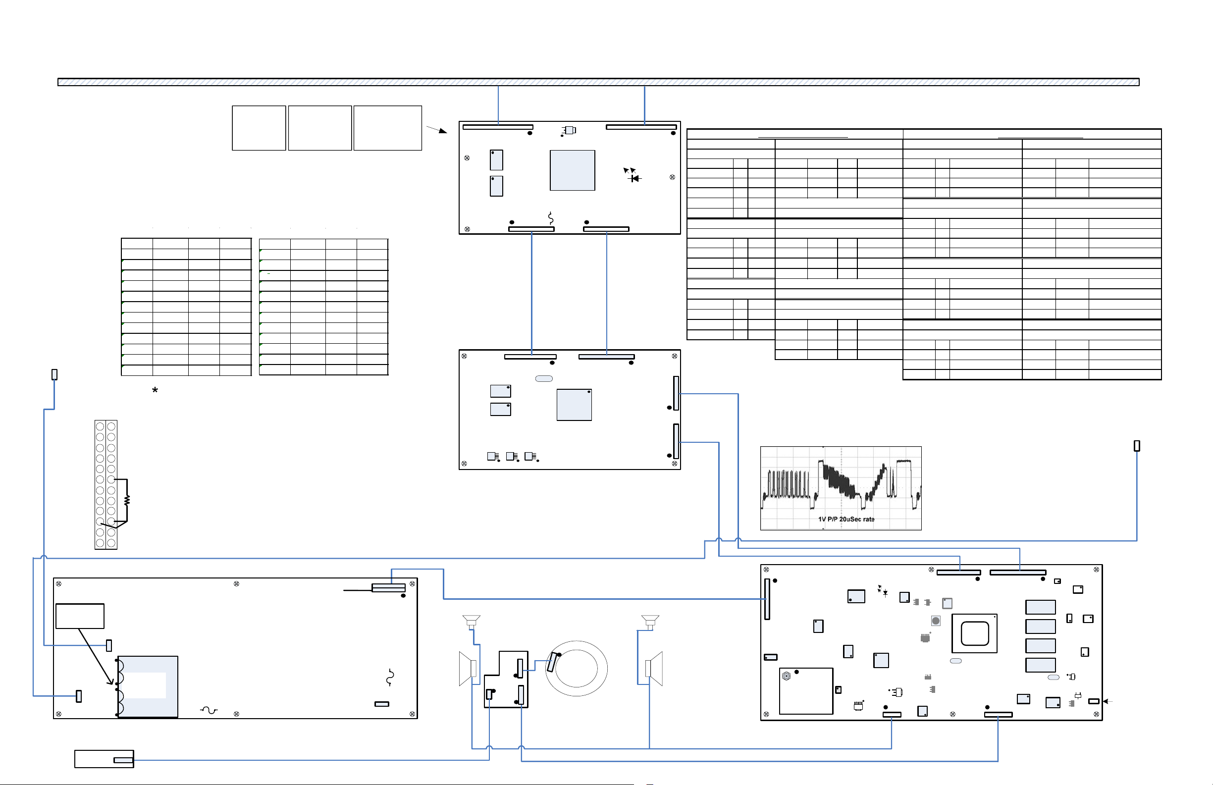
LG 42LG60 Diagram
Left
Backlight
Plug
42LG60 CIRCUIT INTERCONNECT DIAGRAM
TFT PANEL
LD1 Blue LED TFT Drive PWB Check
SET 0FF
LED OFF
Anode
Cathode0V0V
The appearance of LD1 when the set is on appears to be lit dimly.
However there is a small hole in the back panel frame and the
T-CON PWB that allows the backlight to make it appear lit.
BOOT OK
LED ON
Anode
Cathode
11.6V0VAnode
SET ON
LED OFF
Cathode
11.6V
9.5V
CN5 CN4
U15
U16
TFT-Drive (T-CON)
P2 "SMPS" to P801 "Main PWB"
Odd Pins
Pin Label STBY Run
1 16V 0V 16V
3 Gnd Gnd Gnd
5 12V 0V 11.8V
7 Gnd Gnd Gnd
95V5V5.15V
11 5V 5V 5.15V
13 Gnd Gnd Gnd
15 Gnd Gnd Gnd
17 ERR 3.19V 3.3V
19 PWR 0V 2.86V
21 ADIM 0.1V 1.68V
23 SEL 0V 3.2V
PDIM Pin 22 can vary according to OSD Backlight
P2
1
2
3
4
5
6
7
8
9
10
11
12
13
14
15
16
17
18
19
20
21
22
23
24
1st” short either pin 9, 10, 11 or 12 (5V) to Pin 19 (PWR) using a 10K resistor.
This turns on the power supply.
nd
2
: To test the Backlights, jump Pin 20 (INV) to Pin 19 (PWR)
Observe the Backlights.
If normal, the backlights should turn on and off 4 times. Then they go off.
If only ½ the backlights light, (Right side or Left Side), confirm connectors are OK.
If yes, panel defective.
If no backlight activity, confirm the Fuse F700 has approx. 300V on both sides.
If on one side, check fuse for open.
10K
If no 300V, replace Power Supply.
If 300V present, observe the center leg on the left hand side of ballast transformer
T701. Look for 45Khz pulse at 8.7V p/p.
If yes, confirm connectors to backlight OK, if OK, then panel defective.
If no pulse, replace the Power Supply.
setting. 0.9V 0% to 3.3V 100%
Pin Label STBY Run
2 16V 0V 16V
4 Gnd Gnd Gnd
6 12V 0V 11.8V
8 Gnd Gnd Gnd
10 5V 5.15V 5.15V
12 5V 5.15V 5.15V
14 Gnd Gnd Gnd
16 Gnd Gnd Gnd
18 ACD 4V 4.57V
20 INV 0V 3.29V
22 *PDIM 0V 3.38V
24 SYNC 0V 0V
Pins 17, 23 and 24
Not Used
Pin 21 is a
Fixed Voltage
IC108
IC108
5 (1.2V)
4 (1.3V)
3 (0V)
2 (3.37V)
1 (3.29V)
CN1 CN2
P103 P104
IC103
IC102
IC109 IC110
IC109
5 (0V)
4 (1.79V)
3 (0V)
2 (3.36V)
1 (3.29V)
US1
0V
3.2V
1.8V
UC1
F1
3A 125V
11.6V
LVDS
X101
20.25Mhz
IC101
TRU-MOTION
IC110
5 (2.5V)
4 (0V)
3 (0V)
2 (3.3V)
1 (3.37V)
LD1
P101
P102
FRONT SIDE OF MAIN PWB
5V Switching Regulator
In from IC806 1 8.95V In 6,7,8,10 5V 1 0V Source C ST-5V
On/Off 2 3.3V Out 1,2,3,4,5 2.6V Out 2 3.3V Control B RL-ON (PWR)
Out (+5V-TU) 3 5.0V On/Off 17
n/c 4 0.0V
Gnd 5 0.0V
In (+12V) 1 11.6V In 6,7,8,10 5V On/Off 1 Power Control-3.3V Out 3 Low to High to B Q400
Gnd 2 0.0V Out 1,2,3,4,5 1.2V
Out 3 9V On/Off 17
Gnd
Out 2 3.3V Function Pin Volts Name
In 3 5V In 3 5V ST_+5V
IC800
Function Pin Volts Function Pin Volts Name Function Pin Volts Function Pin Volts
IC806 IC820
9V Regulator
Function Pin Volts Function Pin Volts Name Out 4 3.3V (A3.3V-BCM) Gnd 2 0.0V
IC404
3.3V Regulator
Function Pin Volts Out 2 1.8V (+1.8V-NTP) Control B LVDS-Panel-Control
1 0V Gnd 1 Gnd E 0V
2.6V Switching Regulator A2.6V-BCM
Use L801 left side to test output
Use any top pin of IC807 to test input
1.2V Switching Regulator A1.2V-BCM
Use L014 left side to test output
Use any top pin of IC820 to test input
Out 2 3.3V Reset Function Pin Volts Function Pin Volts
Gnd 1 0V Gnd In C ST-5V Source 1, 3 12V
IC807
IC404 uP 3.3V
3.3VST-MICOM
Power Control
Power Control
IC802 (On Back)
3.3V Regulator
Gnd
In 3 5V Gnd E 0V
IC805 (On Back)
3.3V Switching Regulator A3.3V-BCM
Function Pin Volts Function Pin Volts
In 2 5V In 1 3.3VST-MICOM
IC810 (On Back)
1.8V Switching Regulator +1.8V-NTP
Function Pin Volts Function Pin Volts
In 3 3.3V from IC802 Source C 12V
0V
Q802 (On Back)
5V Switch control to Q801
Control B RL-ON (PWR) Control 2, 4 Low from Q902
Gnd E 0V Output 5~8 12V
BACK SIDE OF MAIN PWB
Q801 (On Back)
5V Switch
IC405 uP Reset (On Back)
Reset by Charge of C431
Q902 (On Back)
12V LVDS control to Q901
Q901 (On Back)
12V LVDS On control to P900 Pins 1~4
LVDS
Right
Backlight
Tuner Pin 16 SMTE Color bar In
See back side of page for Waveforms for
P900 using SMTE Color bar as the Input.
Plug
Scope
test point
Backlight pulse over
1000V p/p (45KhZ)
P402
Ballast
Section
P401
Side Control Keys
P100
POWER SUPPY
F700
5A 250V
335V
F700 90V in Stand-By
Pin 24
Pin 23
F101
8A 250V
AC
AC In
P2
Tweeter Tweeter
Ft. PWB
Spk
Assy.
J2
J1
LG
J3
J1
Ft. TOUCH
LED/Push Sw
Spk
5V Pin 3
Video Pin 16
Audio SIF Pin 14
TUNER
MAIN PWB
P801
IC402
Pin 1 ~ 16
TUNER
ATSC/QAM/
NTSC
IC503
116
IC900
IC600
IC701
IC800
IC820
LD803
3.3V BCM
IC805
OK LED
IC500
IC806
P501
*Q902
*IC400
Reset
BCM
*IC805
*IC802
IC501
P800
*Q901
IC100
BCM
X200 (54Mhz)
*IC810
IC807
uP
IC1201
IC304
IC1200
IC202
IC404
Q400
EB
*IC405
P900
IC302
IC300
IC303
IC301
24Mhz
IC1000
P401
X400
IC407
*Grayed out components on the back
P200
Not Used
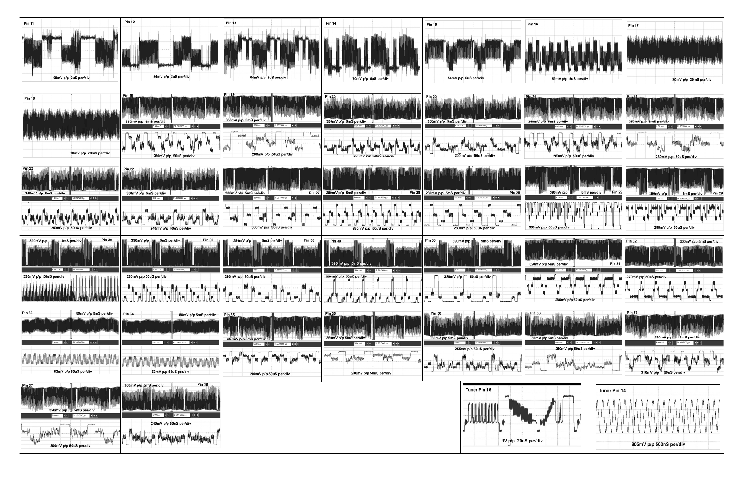
LVDS CABLE P900 FROM MAIN PWB TO CONTROL
PWB P101 USING SMTP COLOR BAR INPUT
LAST TWO WAVEFORMS ARE FROM THE TUNER
Measurements +/- 5%
 Loading...