

Page 1

LCD TV
SERVICE MANUAL
CAUTION
BEFORE SERVICING THE CHASSIS,
READ THE SAFETY PRECAUTIONS IN THIS MANUAL.
CHASSIS : LA73E
MODEL : 42LC7D
42LC7D-UB
R
Page 2

- 2 -
CONTENTS
CONTENTS .............................................................................................. 2
PRODUCT SAFETY ..................................................................................3
SPECIFICATION........................................................................................6
ADJUSTMENT INSTRUCTION................................................................11
TROUBLE SHOOTING & BLOCK DIAGRAM ........................................17
EXPLODED VIEW .................................................................................. 43
REPLACEMENT PARTS LIST ............................................................... 45
SVC. SHEET ...............................................................................................
Page 3
- 3 -
SAFETY PRECAUTIONS
Many electrical and mechanical parts in this chassis have special safety-related characteristics. These parts are identified by in the
Schematic Diagram and Replacement Parts List.
It is essential that these special safety parts should be replaced with the same components as recommended in this manual to prevent
Shock, Fire, or other Hazards.
Do not modify the original design without permission of manufacturer.
General Guidance
An isolation Transformer should always be used during the
servicing of a receiver whose chassis is not isolated from the AC
power line. Use a transformer of adequate power rating as this
protects the technician from accidents resulting in personal injury
from electrical shocks.
It will also protect the receiver and it's components from being
damaged by accidental shorts of the circuitry that may be
inadvertently introduced during the service operation.
If any fuse (or Fusible Resistor) in this TV receiver is blown,
replace it with the specified.
When replacing a high wattage resistor (Oxide Metal Film Resistor,
over 1W), keep the resistor 10mm away from PCB.
Keep wires away from high voltage or high temperature parts.
Before returning the receiver to the customer,
always perform an AC leakage current check on the exposed
metallic parts of the cabinet, such as antennas, terminals, etc., to
be sure the set is safe to operate without damage of electrical
shock.
Leakage Current Cold Check(Antenna Cold Check)
With the instrument AC plug removed from AC source, connect an
electrical jumper across the two AC plug prongs. Place the AC
switch in the on position, connect one lead of ohm-meter to the AC
plug prongs tied together and touch other ohm-meter lead in turn to
each exposed metallic parts such as antenna terminals, phone
jacks, etc.
If the exposed metallic part has a return path to the chassis, the
measured resistance should be between 1MΩ and 5.2MΩ.
When the exposed metal has no return path to the chassis the
reading must be infinite.
An other abnormality exists that must be corrected before the
receiver is returned to the customer.
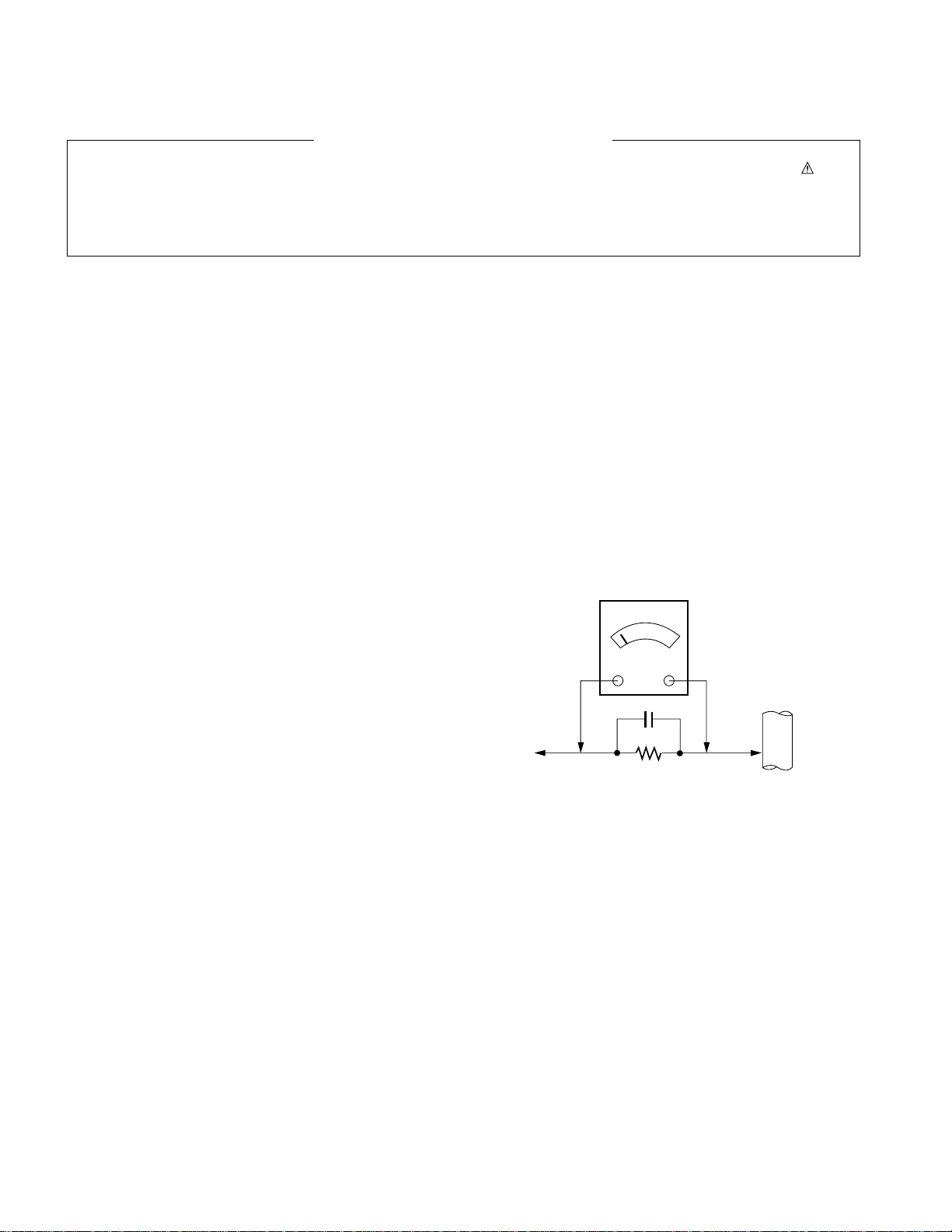
Leakage Current Hot Check (See below Figure)
Plug the AC cord directly into the AC outlet.
Do not use a line Isolation Transformer during this check.
Connect 1.5K/10watt resistor in parallel with a 0.15uF capacitor
between a known good earth ground (Water Pipe, Conduit, etc.)
and the exposed metallic parts.
Measure the AC voltage across the resistor using AC voltmeter
with 1000 ohms/volt or more sensitivity.
Reverse plug the AC cord into the AC outlet and repeat AC voltage
measurements for each exposed metallic part. Any voltage
measured must not exceed 0.75 volt RMS which is corresponds to
0.5mA.
In case any measurement is out of the limits specified, there is
possibility of shock hazard and the set must be checked and
repaired before it is returned to the customer.
Leakage Current Hot Check circuit
T
e
M
IMPORTANT SAFETY NOTICE
0.15uF
o Instrument's
xposed
ETALLIC PARTS
AC Volt-meter
Good Earth Ground
such as WATER PIPE,
CONDUIT etc.
1.5 Kohm/10W
Page 4

- 4 -
CAUTION: Before servicing receivers covered by this service
manual and its supplements and addenda, read and follow the
SAFETY PRECAUTIONS on page 3 of this publication.
NOTE: If unforeseen circumstances create conflict between the
following servicing precautions and any of the safety precautions on
page 3 of this publication, always follow the safety precautions.
Remember: Safety First.
General Servicing Precautions
1. Always unplug the receiver AC power cord from the AC power
source before;
a. Removing or reinstalling any component, circuit board
module or any other receiver assembly.
b. Disconnecting or reconnecting any receiver electrical plug or
other electrical connection.
c. Connecting a test substitute in parallel with an electrolytic
capacitor in the receiver.
CAUTION: A wrong part substitution or incorrect polarity
installation of electrolytic capacitors may result in an
explosion hazard.
2. Test high voltage only by measuring it with an appropriate high
voltage meter or other voltage measuring device (DVM,
FETVOM, etc) equipped with a suitable high voltage probe.
Do not test high voltage by "drawing an arc".
3. Do not spray chemicals on or near this receiver or any of its
assemblies.
4. Unless specified otherwise in this service manual, clean
electrical contacts only by applying the following mixture to the
contacts with a pipe cleaner, cotton-tipped stick or comparable
non-abrasive applicator; 10% (by volume) Acetone and 90% (by
volume) isopropyl alcohol (90%-99% strength)
CAUTION: This is a flammable mixture.
Unless specified otherwise in this service manual, lubrication of
contacts in not required.
5. Do not defeat any plug/socket B+ voltage interlocks with which
receivers covered by this service manual might be equipped.
6. Do not apply AC power to this instrument and/or any of its
electrical assemblies unless all solid-state device heat sinks are
correctly installed.
7. Always connect the test receiver ground lead to the receiver
chassis ground before connecting the test receiver positive
lead.
Always remove the test receiver ground lead last.
8. Use with this receiver only the test fixtures specified in this
service manual.
CAUTION: Do not connect the test fixture ground strap to any
heat sink in this receiver.
Electrostatically Sensitive (ES) Devices
Some semiconductor (solid-state) devices can be damaged easily
by static electricity. Such components commonly are called
Electrostatically Sensitive (ES) Devices. Examples of typical ES
devices are integrated circuits and some field-effect transistors and
semiconductor "chip" components. The following techniques
should be used to help reduce the incidence of component
damage caused by static by static electricity.
1. Immediately before handling any semiconductor component or
semiconductor-equipped assembly, drain off any electrostatic
charge on your body by touching a known earth ground.
Alternatively, obtain and wear a commercially available
discharging wrist strap device, which should be removed to
prevent potential shock reasons prior to applying power to the
unit under test.
2. After removing an electrical assembly equipped with ES
devices, place the assembly on a conductive surface such as
aluminum foil, to prevent electrostatic charge buildup or
exposure of the assembly.
3. Use only a grounded-tip soldering iron to solder or unsolder ES
devices.
4. Use only an anti-static type solder removal device. Some solder
removal devices not classified as "anti-static" can generate
electrical charges sufficient to damage ES devices.
5. Do not use freon-propelled chemicals. These can generate
electrical charges sufficient to damage ES devices.
6. Do not remove a replacement ES device from its protective
package until immediately before you are ready to install it.
(Most replacement ES devices are packaged with leads
electrically shorted together by conductive foam, aluminum foil
or comparable conductive material).
7. Immediately before removing the protective material from the
leads of a replacement ES device, touch the protective material
to the chassis or circuit assembly into which the device will be
installed.
CAUTION: Be sure no power is applied to the chassis or circuit,
and observe all other safety precautions.
8. Minimize bodily motions when handling unpackaged
replacement ES devices. (Otherwise harmless motion such as
the brushing together of your clothes fabric or the lifting of your
foot from a carpeted floor can generate static electricity
sufficient to damage an ES device.)
General Soldering Guidelines
1. Use a grounded-tip, low-wattage soldering iron and appropriate
tip size and shape that will maintain tip temperature within the
range or 500
F to 600 F.
2. Use an appropriate gauge of RMA resin-core solder composed
of 60 parts tin/40 parts lead.
3. Keep the soldering iron tip clean and well tinned.
4. Thoroughly clean the surfaces to be soldered. Use a mall wirebristle (0.5 inch, or 1.25cm) brush with a metal handle.
Do not use freon-propelled spray-on cleaners.
5. Use the following unsoldering technique
a. Allow the soldering iron tip to reach normal temperature.
(500
F to 600 F)
b. Heat the component lead until the solder melts.
c. Quickly draw the melted solder with an anti-static, suction-
type solder removal device or with solder braid.
CAUTION: Work quickly to avoid overheating the
circuitboard printed foil.
6. Use the following soldering technique.
a. Allow the soldering iron tip to reach a normal temperature
(500
F to 600 F)
b. First, hold the soldering iron tip and solder the strand against
the component lead until the solder melts.
c. Quickly move the soldering iron tip to the junction of the
component lead and the printed circuit foil, and hold it there
only until the solder flows onto and around both the
component lead and the foil.
CAUTION: Work quickly to avoid overheating the circuit
board printed foil.
d. Closely inspect the solder area and remove any excess or
splashed solder with a small wire-bristle brush.
SERVICING PRECAUTIONS
Page 5

- 5 -
IC Remove/Replacement
Some chassis circuit boards have slotted holes (oblong) through
which the IC leads are inserted and then bent flat against the
circuit foil. When holes are the slotted type, the following technique
should be used to remove and replace the IC. When working with
boards using the familiar round hole, use the standard technique
as outlined in paragraphs 5 and 6 above.
Removal
1. Desolder and straighten each IC lead in one operation by gently
prying up on the lead with the soldering iron tip as the solder
melts.
2. Draw away the melted solder with an anti-static suction-type
solder removal device (or with solder braid) before removing the
IC.
Replacement
1. Carefully insert the replacement IC in the circuit board.
2. Carefully bend each IC lead against the circuit foil pad and
solder it.
3. Clean the soldered areas with a small wire-bristle brush.
(It is not necessary to reapply acrylic coating to the areas).
"Small-Signal" Discrete Transistor
Removal/Replacement
1. Remove the defective transistor by clipping its leads as close as
possible to the component body.
2. Bend into a "U" shape the end of each of three leads remaining
on the circuit board.
3. Bend into a "U" shape the replacement transistor leads.
4. Connect the replacement transistor leads to the corresponding
leads extending from the circuit board and crimp the "U" with
long nose pliers to insure metal to metal contact then solder
each connection.
Power Output, Transistor Device
Removal/Replacement
1. Heat and remove all solder from around the transistor leads.
2. Remove the heat sink mounting screw (if so equipped).
3. Carefully remove the transistor from the heat sink of the circuit
board.
4. Insert new transistor in the circuit board.
5. Solder each transistor lead, and clip off excess lead.
6. Replace heat sink.
Diode Removal/Replacement
1. Remove defective diode by clipping its leads as close as
possible to diode body.
2. Bend the two remaining leads perpendicular y to the circuit
board.
3. Observing diode polarity, wrap each lead of the new diode
around the corresponding lead on the circuit board.
4. Securely crimp each connection and solder it.
5. Inspect (on the circuit board copper side) the solder joints of
the two "original" leads. If they are not shiny, reheat them and if
necessary, apply additional solder.
Fuse and Conventional Resistor
Removal/Replacement
1. Clip each fuse or resistor lead at top of the circuit board hollow
stake.
2. Securely crimp the leads of replacement component around
notch at stake top.
3. Solder the connections.
CAUTION: Maintain original spacing between the replaced
component and adjacent components and the circuit board to
prevent excessive component temperatures.
Circuit Board Foil Repair
Excessive heat applied to the copper foil of any printed circuit
board will weaken the adhesive that bonds the foil to the circuit
board causing the foil to separate from or "lift-off" the board. The
following guidelines and procedures should be followed whenever
this condition is encountered.
At IC Connections
To repair a defective copper pattern at IC connections use the
following procedure to install a jumper wire on the copper pattern
side of the circuit board. (Use this technique only on IC
connections).
1. Carefully remove the damaged copper pattern with a sharp
knife. (Remove only as much copper as absolutely necessary).
2. carefully scratch away the solder resist and acrylic coating (if
used) from the end of the remaining copper pattern.
3. Bend a small "U" in one end of a small gauge jumper wire and
carefully crimp it around the IC pin. Solder the IC connection.
4. Route the jumper wire along the path of the out-away copper
pattern and let it overlap the previously scraped end of the good
copper pattern. Solder the overlapped area and clip off any
excess jumper wire.
At Other Connections
Use the following technique to repair the defective copper pattern
at connections other than IC Pins. This technique involves the
installation of a jumper wire on the component side of the circuit
board.
1. Remove the defective copper pattern with a sharp knife.
Remove at least 1/4 inch of copper, to ensure that a hazardous
condition will not exist if the jumper wire opens.
2. Trace along the copper pattern from both sides of the pattern
break and locate the nearest component that is directly
connected to the affected copper pattern.
3. Connect insulated 20-gauge jumper wire from the lead of the
nearest component on one side of the pattern break to the lead
of the nearest component on the other side.
Carefully crimp and solder the connections.
CAUTION: Be sure the insulated jumper wire is dressed so the
it does not touch components or sharp edges.
Page 6

- 6 -
SPECIFICATION
NOTE : Specifications and others are subject to change without notice for improvement
.
4. General Specification(TV)
No. Item Specification Remark
1. Receiving System ATSC/64 & 256 QAM/ NTSC-M
2. Available Channel 1) VHF : 02~13
2) UHF : 14~69
3) DTV : 02-69
4) CATV : 01~135
5) CADTV : 01~135
3. Input Voltage 1) AC 100 ~ 240V 50/60Hz
4. Market NORTH AMERICA
5. Screen Size 26 inch Wide – 26 inches(582.96mm) For 26LC7D-UB
32 inch Wide - 31.51inches(800.4mm) For 32LC7D-UB,32LC4D-UA
37 inch Wide – 32.02 inches(940.3mm) For 37LC7D-UB
42 inch Wide – 42.02 inches(1067.308mm) For 42LC7D-UB,42LC4D-UA
6. Aspect Ratio 16:9
7. Tuning System FS
8. LCD Module T260XW02-V5 For 26LC7D-UE
LC320WX4-SLA1 For 32LC7D-UB,32LC4D-UA
LC370WX3-SLA1 For 37LC7D-UB
LC420WX6-SLA1 For 42LC7D-UB,42LC4D-UA
9. Operating Environment 1) Temp : 0 ~ 40 deg
2) Humidity : ~ 80 %
10. Storage Environment 1) Temp : -20 ~ 60 deg
2) Humidity : 0 ~ 90 %
1. Application Range.
This spec sheet is applied to the 37"/42" LCD TV used LA73E
chassis.
2. Especificación
Each part is tested as below without special appointment
2.1 Temperature : 20 ±5°C
2.2 Relative Humidity : 65 ±10%
2.3 Power Voltage : Standard input voltage
(100~240V@ 50/60Hz)
• Standard Voltage of each products is marked by models
2.4 Specification and performance of each parts are followed
each drawing and specification by part number in
accordance with BOM .
2.5 The receiver must be operated for about 20 minutes prior
to the adjustment.
3. Test method
3.1 Performance : LGE TV test method followed.
3.2 Demanded other specification
Safety : UL, CSA, IEC specification
3.3 EMC : FCC, ICES, IEC specification
Page 7

- 7 -
5. Chroma & Brightness
5-1. 37LC7D-UB
CONDITION : EZ-Picture "Daylight"
5-2. 42LC7D-UB, 42LC4D-UA
CONDITION : EZ-Picture "Daylight"
No Item Min Typ Max Unit Remark
1. White peak brightness 360 450 cd/m
2
HDMI input, full white,
Video Black level=High
2. Contrast ratio 700:1 900:1 Non dimming mode
(PC Mode)
3000:1 4000:1 5000:1 Dimming mode
1. Input full black, wait 10 minute
,
measure black level
2. Input full white , wait 10 minute,
measure white level
3. Brightness uniformity 1.3 Refer to LCD SPEC.
4. Color coordinate RED X 0.633 +/- 0.03
Y 0.339 +/- 0.03
GREEN X 0.286 +/- 0.03
Y 0.610 +/- 0.03
BLUE X 0.147 +/- 0.03
Y 0.065 +/- 0.03
WHITE X 0.276 +/- 0.03
Y 0.283 +/- 0.03
5. Viewing angle 178 R/L, U/D
6. Color Temperature Standard 8,300 9,300 10,300 <Test Signal>
Cool 10,000 11,000 12,000
HDMI input, With 16-gray pattern
Warm 5,500 6,500 7,500 6thbar from right
No Item Min Typ Max Unit Remark
1. White peak brightness 360 450 cd/m
2
HDMI input, full white,
Video Black level=High
2. Contrast ratio 800:1 1000:1 Non dimming mode
(PC Mode)
3000:1 4000:1 5000:1 Dimming mode
1. Input full black, wait 10 minute
,
measure black level
2. Input full white , wait 10 minute,
measure white level
3. Brightness uniformity 1.3 Refer to LCD SPEC.
4. Color coordinate RED X 0.633 +/- 0.03
Y 0.339 +/- 0.03
GREEN X 0.286 +/- 0.03
Y 0.610 +/- 0.03
BLUE X 0.147 +/- 0.03
Y 0.065 +/- 0.03
WHITE X 0.276 +/- 0.03
Y 0.283 +/- 0.03
5. Viewing angle 178 R/L, U/D
6. Color Temperature Standard 8,300 9,300 10,300 <Test Signal>
Cool 10,000 11,000 12,000 HDMI input,
Warm 5,500 6,500 7,500 Daylight/Cool 85 IRE
Page 8

- 8 -
6. Component Video Input (Y, PB
, PR)
No.
Specification
Remark
Resolution H-freq(kHz) V-freq(Hz)
1. 720*480 15.73 59.94 SDTV ,DVD 480I
2. 720*480 15.73 60.00 SDTV ,DVD 480I
3. 720*480 31.47 59.94 SDTV 480P
4. 720*480 31.50 60.00 SDTV 480P
5. 1280*720 44.96 59.94 HDTV 720P
6. 1280*720 45.00 60.00 HDTV 720P
7. 1920*1080 33.72 59.94 HDTV 1080I
8. 1920*1080 33.75 60.00 HDTV 1080I
9. 1920*1080 27 24 HDTV 1080P
10. 1920*1080 33.75 30 HDTV 1080P
No.
Specification
Remark
Resolution H-freq(kHz) V-freq(Hz)
Pixel clock(MHz)
PC DDC
1. 640*350 31.469 70.08 25.17 DOS
2. 720*400 31.469 70.08 28.32 DOS O
3. 640*480 31.469 59.94 25.17 VESA(VGA) O
4. 800*600 37.879 60.31 40.00 VESA(SVGA) O
5. 1024*768 48.363 60.00 65.00 VESA(XGA) O
6. 1280*768 47.776 59.87 79.50 CVT(WXGA) O
7. 1360*768 47.720 59.799 84.75 CVT(WXGA) O
8. 1366*768 47.13 59.65 72
7. RGB PC
- RGB PC INPUT Mode Table
- HDMI INPUT(PC/DTV)
No. Resolution H-freq(kHz) V-freq(Hz) Pixel clock(MHz) Remark
PC DDC
1. 640*480 31.469 59.94 25.17 VESA(VGA) O
2. 800*600 37.879 60.31 40.00 VESA(SVGA) O
3. 1024*768 48.363 60.00 65.00 VESA(XGA) O
4. 1280*768 47.776 59.87 79.50 CVT(WXGA) O
5. 1360*768 47.720 59.799 84.75 CVT(WXGA) O
6. 1366*768 47.13 59.65 72
DTV
7. 720*480 31.469 59.94 27.00 SDTV 480P
8. 720*480 31.500 60.00 27.03 SDTV 480P
9. 1280*720 44.96 59.94 74.17 HDTV 720P
10. 1280*720 45.00 60.00 74.25 HDTV 720P
11. 1920*1080 33.72 59.94 74.17 HDTV 1080I
12. 1920*1080 33.75 60.00 74.25 HDTV 1080I
13. 1920*1080 27 24.00 74.25 HDTV 1080P
14. 1920*1080 33.75 30.00 74.25 HDTV 1080P
Page 9

- 9 -
8. Mechanical specification
1) 37LC7D
No. Item Content Unit Remark
1. Product Widt(W) Length(D) Height(H) mm
Dimension Before Packing 927 280.5 692.8 mm With Stant
After Packing 999 264 874 mm
2. Product Only SET 20 Kg
With BOX 25 Kg
2) 42LC7D
No. Item Content Unit Remark
1. Product Widt(W) Length(D) Height(H) mm
Dimension Before Packing 1033.4 287.6 750 mm With Stant
After Packing 1119 374 858 mm
2. Product Only SET 24.9 Kg
With BOX 30.4 Kg
Page 10

- 10 -
9. Customer Menu Setup (Shipment Condition)
No Item Condition Remark
1. Input Mode TV02CH
2. Volume Level 30
3. Mute Off
4. Aspect Ratio 16:9
5. Video EZ Picture Daylight
Contrast 100
Brightness 40
Color 70
Sharpness 70
Tint 0
Color-temperature Cool
XD Auto(On)
Advanced Cinema3:2 Mode(Off)
Black Level(RF,HDMI=>Low),(AV=>High)( RGB-PC,Component=>Disable)
6. Audio Audio Language Off
EZ Sound Normal
Balance 0
Bass 50
Front Surround Off
TV Speaker On
7. Timer Auto clock Off
Manual Clock Off
Off Timer Off
On Timer Off
Sleep Timer Off
Auto Off Off
8. Option Aspect Ratio 16:9
Caption/Text Off
Caption Option Set By Program
Language English
Simplink On
9. Lock Lock System Off
Set password On
(Default:0000)
Block channel None
Movie Rating Off
TV Rating-Children None
TV Rating-General None
Input Block Off
10. Channel Memory RF : 2, 3, 4, 5, 6, 7, 8, 9, 10, 11, 12, 13, 14, 30, 51, 63
CATV : 15, 16, 17
Page 11
- 11 -
ADJUSTMENT INSTRUCTION
1. Application Object
These instructions are applied to all of the LCD TV, LA73E.
2. Notes
(1) Because this is not a hot chassis, it is not necessary to use
an isolation transformer. However, the use of isolation
transformer will help protect test equipment.
(2) Adjustments must be done in the correct order.
(3) The adjustments must be performed in the circumstance of
20±5°C of temperature and 65±10% of relative humidity if
there is no specific designation.
(4) The input voltage of the receiver be must kept 110V, 60Hz
when adjusting.
(5) The receiver must be operational for about 15 minutes
prior to the adjustments.
Perform preliminary operation after receiving 100% White
Pattern (06CH).
(Or 3. White Pattern status of Ez-Adjust)
White Pattern entry method
A) Enter into Ez-Adjust by pressing the ADJ key on the
adjustment R/C.
B) 100% FULL WHITE PATTERN appears if pressing the
OK (
) key after selecting the 3.WHITE PATTERN with
the CH + / - KEY.
* It is possible to heat run the set without a separate
signal generator in this mode.
Caution : Care must be taken as afterimage
phenomena may occur about the black level part of
screen If leaving pause image turned on for more
than 20 minutes (especially inner digital pattern (13
CH), Cross Hatch Pattern (09CH) with significant
black/white contrast).
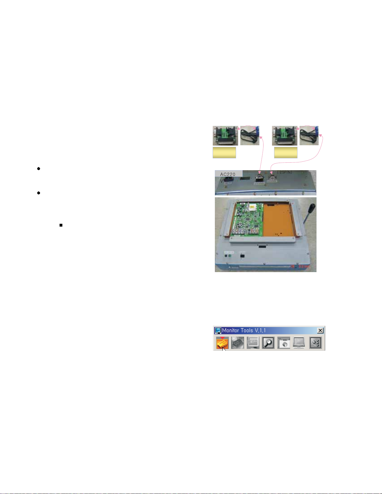
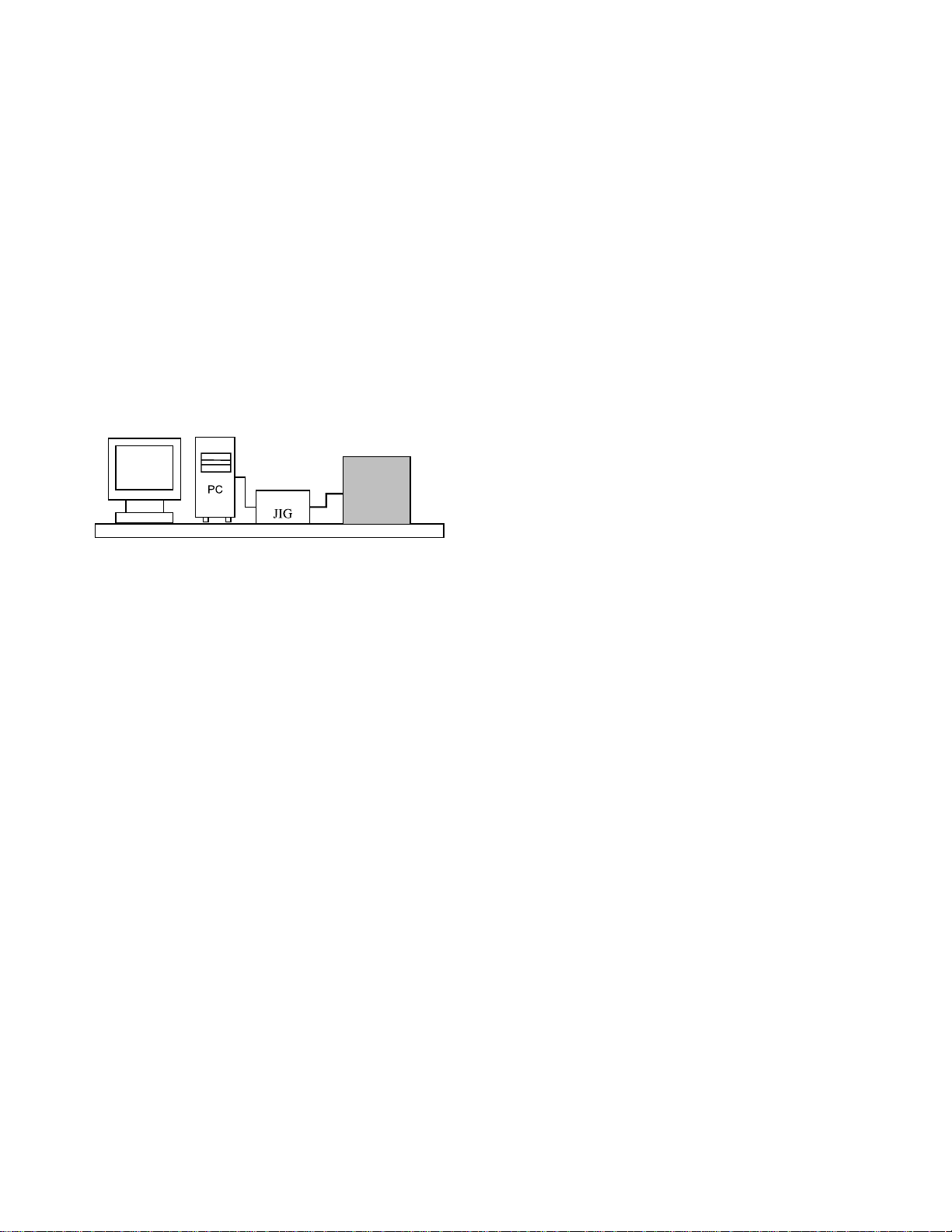
3. MICOM Download(Option)
3-1. Required Test Equipment
(1) JIG-LEVER TYPE for adjusting: 1EA
(2) PC & MONITOR: 2EA
(3) BOARD for INTERFACE: IIC & ISP BOARD: 2EA
(4) 15P D-SUB CABLE: 2EA
(5) Using the 12/15 line of D-SUB 15P
12-SDA/15-SCL
3-2. JIG Connection
3-3. Establishment Program
(1) Establish LGE Monitor Tools v1.1
(2) The program work and it is opened program window as
seen below.
connection
to PC
connection
to PC
Page 12
- 12 -
(3) Click the first icon shown in fig.9. The window seen in
fig.10 should appear.
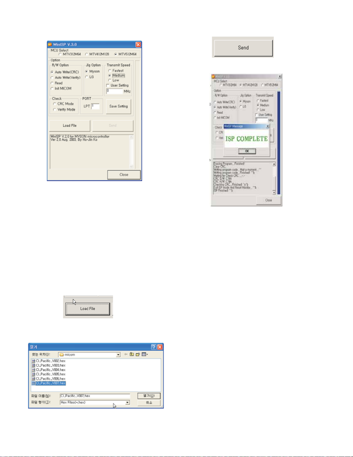
3-4. Set Method
(1) MCU Select: MTV512M64
(2) Option
R/W Option: Auto Write(Verity)
Jig Option: Myson
Transmit Speed: Medium
(3) Check: Just do it with blank micom.
(4) PORT
Chose Parallel Port (normal LPT1)
Attention: You must chose EPP when select Rom BIAS at
LPT
3-5. Download Method
(1) Click the Load File.
(2) Locate and select the correct file from your computer.
(*.hex).
(3) Click the Send.
(4) When you see (ISP COMPLETE) the download is
complete.
Page 13
- 13 -
6. ADC-Set Adjustment
6-1. Synopsis
ADC-Set adjustment to set the black level and the Gain to
optimum.
6-2. Test Equipment
Service R/C, 801GF(802V, 802F, 802R) or MSPG925FA
Pattern Generator
(480i/1080i The Horizontal 100% Color Bar Pattern adjust to
within 0.7±0.1Vp-p)
[ADC adjustment (MSPG-925Fx series) Model No. & Pattern No.]
- Model No.: #209(480i adjustment), #223(1080i adjustment)
- Pattern No.: #65(7ColorBar Pattern)
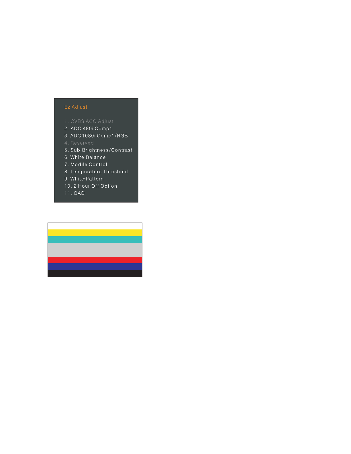
6-3. Adjustment
(1) Select Component1 as the input with 100% Horizontal
Color Bar Pattern(HozTV31Bar) in 480i Mode
(2) After receiving signal for at least 1 second, press the ADJ
Key on the Service R/C to enter the ‘Ez - Adjust’ and select
the ‘2. ADC 480i Comp1’.
Pressing the Enter Key to adjust automatically.
(3) When the adjustment is over, 'MST3361 Component
Success’ is displayed. If the adjustment has errors,
'MST3361 Configuration Error’ is displayed.
(4) Select Component1 as the input with 100% Horizontal
Color Bar Pattern(HozTV31Bar) in 1080i Mode.
(5) After receiving signal for at least 1 second, press the ADJ
Key on the Service R/C to enter the ‘Ez - Adjust’ and select
the ‘3. ADC 1080i Comp1/RGB’.
Pressing the Enter Key to adjust automatically.
(6) When the adjustment is over, 'MST3361 Component
Success’ is displayed. If the adjustment has errors,
'MST3361 Configuration Error’ is displayed.
(7) After the Component MST3361 adjustment is over, convert
the RGB-DTV Mode and display Pattern.
When the adjustment is over, 'MST3361 RGB_DTV
Success’ is displayed.
(8) Readjust after confirming the case Pattern or adjustment
condition where the adjustment errors.
(9) After adjustment is complete, exit the adjustment mode by
pressing the ADJ KEY.
<Fig. 2> Adjustment Mode
<Fig. 3> Adjustment Pattern: 480i/1080i 60Hz HozTV30 Bar
Pattern
Page 14
- 14 -
7. EDID(The Extended Display
Identification Data)/DDC
(Display Data Channel) Download
This is the function that enables “Plug and Play".
7-1. HDMI EDID Data Input
(1) Required Test Equipment
1) PC, Jig for adjusting DDC. (PC serial to D-sub
Connection equipment)
2) S/W for writing DDC(EDID data write & read)
3) D-Sub cable
4) Jig for HDMI Cable connection
(2) Preparation for Adjustments &
Setting of Device
1) Set devices as below and turn on the PC and JIG.
2) Open S/W for writing DDC (EDID data write & read).
(operated in DOS mode)
7-2. EDID DATA for LA73E
:EDID for HDMI-1 (DDC (Display Data Channel) Data)
EDID Block 0 table =
EDID Block 1 table =
:EDID for HDMI-2 (DDC (Display Data Channel) Data)
EDID Block 0 table =
EDID Block 1 table =
:EDID for RGB-PC
EDID Block 0 table =
0 | 00 FF FF FF FF FF FF 00 1E 6D 01 00 01 01 01 01
10 | 00 11 01 03 80 73 41 96 0A CF 74 A3 57 4C B0 23
20 | 09 48 4C 2F CE 00 31 40 45 40 61 40 01 01 01 01
30 | 01 01 01 01 01 01 66 21 50 B0 51 00 1B 30 40 70
40 | 36 00 C4 8E 21 00 00 1E 0E 1F 00 80 51 00 1E 30
50 | 40 80 37 00 C4 8E 21 00 00 1C 00 00 00 FD 00 38
60 | 4B 1F 3C 09 00 0A 20 20 20 20 20 20 00 00 00 FC
70 | 00 4C 47 20 54 56 0A 20 20 20 20 20 20 20 01 98
0 | 02 03 16 F1 46 84 05 03 02 20 22 23 15 07 50 66
10 | 03 0C 00 10 00 80 01 1D 00 72 51 D0 1E 20 6E 28
20 | 55 00 C4 8E 21 00 00 1E 01 1D 80 18 71 1C 16 20
30 | 58 2C 25 00 C4 8E 21 00 00 9E 8C 0A D0 8A 20 E0
40 | 2D 10 10 3E 96 00 C4 8E 21 00 00 18 8C 0A D0 8A
50 | 20 E0 2D 10 10 3E 96 00 13 8E 21 00 00 18 00 00
60 | 00 00 00 00 00 00 00 00 00 00 00 00 00 00 00 00
70 | 00 00 00 00 00 00 00 00 00 00 00 00 00 00 00 25
0 | 00 FF FF FF FF FF FF 00 1E 6D 01 00 01 01 01 01
10 | 00 11 01 03 80 73 41 96 0A CF 74 A3 57 4C B0 23
20 | 09 48 4C 2F CE 00 31 40 45 40 61 40 01 01 01 01
30 | 01 01 01 01 01 01 01 1D 00 72 51 D0 1E 20 6E 28
40 | 55 00 C4 8E 21 00 00 1E 01 1D 80 18 71 1C 16 20
50 | 58 2C 25 00 C4 8E 21 00 00 9E 00 00 00 FC 00 4C
60 | 47 20 54 56 0A 20 20 20 20 20 20 20 00 00 00 FD
70 | 00 38 4B 1F 3C 09 00 0A 20 20 20 20 20 20 01 66
0 | 02 03 16 F1 46 84 05 03 02 20 22 23 15 07 50 66
10 | 03 0C 00 20 00 80 8C 0A D0 8A 20 E0 2D 10 10 3E
20 | 96 00 C4 8E 21 00 00 18 8C 0A D0 8A 20 E0 2D 10
30 | 10 3E 96 00 13 8E 21 00 00 18 00 00 00 00 00 00
40 | 00 00 00 00 00 00 00 00 00 00 00 00 00 00 00 00
50 | 00 00 00 00 00 00 00 00 00 00 00 00 00 00 00 00
60 | 00 00 00 00 00 00 00 00 00 00 00 00 00 00 00 00
70 | 00 00 00 00 00 00 00 00 00 00 00 00 00 00 00 B3
0 | 00 FF FF FF FF FF FF 00 1E 6D 01 00 01 01 01 01
10 | 00 11 01 03 68 73 41 96 0A CF 30 A3 57 4C B0 23
20 | 09 50 4E A1 08 00 01 01 01 01 01 01 01 01 01 01
30 | 01 01 01 01 01 01 66 21 50 B0 51 00 1B 30 40 70
40 | 36 00 C4 8E 21 00 00 1E 0E 1F 00 80 51 00 1E 30
50 | 40 80 37 00 C4 8E 21 00 00 1C 00 00 00 FD 00 38
60 | 4B 1F 3C 09 00 0A 20 20 20 20 20 20 00 00 00 FC
70 | 00 4C 47 20 54 56 0A 20 20 20 20 20 20 20 00 D0
LCD TV SET
(or Digital Board)
Page 15

- 15 -
8. Adjustment of White Balance
8-1. The Purpose and Principal of Color
Temperature Adjustment
(1) Purpose: to reduce the difference in color temperature
among modules
(2) Principal: A module is in full dynamic range when RGB
Gain on OSD is 192. To adjust the white balance without
causing full dynamic range and full data, fix one of RGB
Gains at 192 and control the other two by reducing them
from 192.
8-2. Required Equipment
(1) Color Analyzer : CA-110 or CA-210
(2) Automatic adjustor (with automatic adjustment necessity
and the RS-232C communication being possible)
8-3. Connection Diagram of Equipment
for Measuring
(Automatic Adjustment)
Use the internal pattern to adjust White Balance. The pattern
is automatically given when the automatic adjustment device
is connected or when a user presses ADJ on the remote
controller to start Ez Adjust and then selects 6.White-Balance.
[ Requirements for Automatic Adjustment
(1) The illuminance of surroundings
10 lux or less; preventing light in surroundings as much as
possible
(2) The location of the Probe
1) For PDP: place the color analyzer (CA-110, CA-210)
close to the surface of a module and start the
adjustment.
2) For LCD: place the color analyzer (CA-110, CA-210)
close to the surface of a module within 10 cm and keep
the probe of the color analyzer at 80° to 100° angle from
the surface of a module.
(3) Aging time
1) Once Aging is started, keep the power on without power
supply interruption for at least 15 minutes for heat run.
2) For PDP, use the internal pattern to adjust White
Pattern.
3) For LCD, use NO SIGNAL or Full White Pattern to
ensure the backlight is turned on.
8-4. Adjustment of White Balance
(Automatic Adjustment)
(1) Turn on the POWER ON( ) of the remote controller to set
the adjustment and then start the automatic adjustment or
set the Baud Rate to 115200.Â) of the remote controller to
(2) Start the adjustment from “wb 00 00” and complete it at
“wb 00 ff”. (Adjust the offset if necessary)
wb 00 00 the automatic adjustment of White Balance is
started.
wb 00 10 adjusting gain (internal pattern appears) is
started.
ja 00 ff adjusting data
jb 00 c0
...
wb 00 1f adjusting gain is completed.
Adjust the offset (from wb 00 20 to wb 00 2f) if necessary.
wb 00 ff the automatic adjustment of White Balance
(internal pattern disappears) is completed.
Connection Diagram of Automatic Adjustment
Full W hite Pattern
RS-232C
CA-100+
COL OR
ANALYZER
TYPE; CA-100+
Page 16

- 16 -
[[
RS-232C Command
(Automatic Adjustment)
LA73E Chassis Model All]
8-5. Adjustment of White Balance
(Manual Adjustment)
Required Equipment : CA-210
(1) Enter ‘Ez - Adjust’ by pressing ADJ KEY on the Service
Remote Control.
(2) Select "9. TEST PATTERN" using CH +/- Key and HEAT
RUN at least 30 minutes by pressing the ENTER Key.
(3) Zero Calibrate of the Color Analyzer, then attach sensor to
LCD module surface when you adjust.
(4) Select ‘6. White-Balance’ of ‘Ez - Adjust’ by pressing the
ADJ KEY on the Service R/C. Then enter adjustment mode
by pressing the Right KEY (
G
) .
(The internal pattern of full white appears by pressing
G
)
(5) The adjustment is conducted in three levels of color
temperature; COOL, MEDIUM, and WARM.
[ Color temperature: Cool, Medium, Warm
(1) When R Gain is fixed at 192,
Control G Gain and B Gain by reducing them from 192.
(2) When B Gain is fixed at 192,
Control R Gain and G Gain by reducing them from 192.
(3) When G Gain is fixed to 192,
Control R Gain and B Gain by reducing them from 192.
Fix one of three Gains (R Gain, G Gain, and B Gain) at 192
and control the other two by reducing values from 192 to
prevent it from increasing.
(When RGB Gains are all 192, the module is in full dynamic
range.)
R Gain
G Gain
B Gain
R Cut
G Cut
B Cut
jg
jh
ji
Cool
ja
jb
jc
Mid
RS-232C COMMAND
[CMD ID DATA]
CENTER
(DEFAULT)(Decimal)
jd
je
jf
00
00
00
192
192
192
Warm
Min
Max
(Deci
mal)
64
64
64
Cool
64
64
64
Mid
64
64
64
Warm
9. USB S/W Download (Option)
9-1. Overview
USB Download enables quick response to S/W upgrading
and helps to configure the panel to the latest updates.
9-2. How to Download
(1) Before starting USB download, ensure that the power is
turned off and the display is turned on.
(2) Once the USB memory stick containing the upgraded file
is connected to the USB port on the main board, the
following picture appears on the screen.
(3) Check the current version at [Current TV Software Version
Information] and the target version at [New Found TV
Software Version Information]. Press Enter on the remote
controller to confirm the upgrade.
(4) The following picture shows the downloading in progress.
Once the download is completed, the power is
automatically turned on and off. (Otherwise, please turn
the power on and off)
(5) Once the download is completed, remove the USB
memory stick from the USB port. Press IN-START on the
remote controller to check the upgraded S/W version at
the top of the screen while the display is turned on.
<S/W Upgrade Screen>
<Downloading in progress Screen>
Do not plug off.
Press EXIT to cancel the upgrade.
The software upgrade is now in progress.
Until the whole process if completed, please.
- Do not remove the memory card from the slot.
- Do not plug off.
Reading the file---Done
Upgrading---Done
The TV will restart automatically in 0 seconds.
Page 17

- 17 -
TROUBLESHOOTING & BLOCK DIAGRAM
- Prouct Brief spec
RGB In (15 Pin)
Others
1 RF(Air /Cable)RF
O(PSIP)Program Guide Type
YesXD Engine
Yes(2D)Enhanced Noise Reduction
YesAdaptive Picture Mode
YesSRS Trusurround TX
YesBBE
YesAuto Navigation (Link)
NoRGB DTV
DOS70,VGA60,S
VGA60,
XGA60,WXGA60,
SXGA60
¥Audio Output
10W*2
¥Freeze No
RemarkBroadcomFeature
1 RF
Use Brief Info
USE scalier On/Off OSD Menu
Phase, SizeAdjust
Page 18

- Block diagram for CI DTV
- 18 -
12
EEP
Audio
ROM
X-tal
54MHz
256Mbit
SDRAM
256Mbit
SDRAM
RS-232C
64-Bit I/F
USB for upgrade S/W
BCM3560
VSB/QAM/NTSC/SIF
LVDS
Trans
Digital Output.
VDEC_CVBS/S_Y
SPDIF Out
SPDIF_OUT
I2S Audio Input
Audio
PWM L/R
I2S Output
DVI Input
16MB
Flash Memory
LR
MNT_Out
(MTV416)
(MTV416)
Sub Micom
Sub Micom
IIC
AUDIO DAC
IIS
HDMI/DVI
Tuner
CableANT.
SIF for NTSC
ATSC/NT
SC Tuner
Reset IC
S
B
V
C
CXA2069(AV S/W)
SIF for NTSC
V, LR
Rear AV
IF P/N for DTV
IN5
IN1
YC, LR
Rear S
IN1
V,LR
Side AV
Y,C
CVBS
OUT1
IN4
YC, LR
Side S
IN4
I2S
Audio R/L
IN4
IN3
OUT3
LR
LR
LR
MNT_V_Out
RGB(Phone)
Comp_1
Comp_2
SPDIF
Data [24]
Hsync/Vsync/DE/Clk
AUDIO ADC
HDMI & Component
HDCP
RGB-PC
MST3361
H/V Sync
2X1
S/W
R/G/B
2X1
S/W
YCbCr
YCbCr
Comp_1
Comp_2
TMDS
TMDS
DDS
DDS
Page 19

- 19 -
- Powr flow diagram
5V_PANEL
CMO, AUO
CMO, AUO
MP1593
MP1593
MST3361
MST3361
BCM3560
M62320FP
M62320FP
LM75CIMX
LM75CIMX
MM1732
MM1732
+2.5V_MST
SC1566-2.5
SC1566-2.5
BCM3560
A1.2V_BCM, D1.2V_BCM
DDC
DDC
SI4925DY
SI4925DY
FAN4
FAN4
KIA78R09
KIA78R09
FAN1,2,3
FAN1,2,3
MC3307
MC3307
+5.0V
CS5331A
CS5331A
CS4344
CS4344
AT24C02N
AT24C02N
AT24C512W
AT24C512W
74F08D
74F08D
TPS2042
TPS2042
FMS6400
FMS6400
FMS6407
FMS6407
+5V_TU
D3.3V_BCM
FSA1156
FSA1156
TUNER
TUNER
BCM3560
BCM3560
3.3VST_MICOM
BCM3560
BCM3560
3.3V_MST
MST3361
MST3361
A2.6V_BCM
SC1566-2.5
SC1566-2.5
74LVC14A
74LVC14A
HYDU561622
HYDU561622
THC63LVD
THC63LVD
MTV416GMF
MTV416GMF
BCM3560
BCM3560
D2.6V_BCM
S29GL128M
S29GL128M
P_+19V
P_+19V
TPA3100
TPA3100
+12.0V
+12.0V
KIA78R09
KIA78R09
PQ05DZ1U
PQ05DZ1U
CXA2069
CXA2069
+9.0V
+9.0V
+6.0V
+6.0V
AZ1117H-3.3
AZ1117H-3.3
ST_5V
ST_5V
BA033FP
BA033FP
A3.3V_BCM
A3.3V_BCM
BCM3560
BCM3560
BCM3560
SC1566-2.5
SC1566-2.5
+3.3V
+3.3V
BCM3560
Page 20

- 20 -
- 12C Control block diagram
0x90
0xA6
I2C Address
0xC2
0x74
0x9C
0x1C
0x50
M62320
AV S/W(CXA2069)
5.0V
4.7K J
Main EEPROM
5.0V
ATSC/NTSC Tuner
I2C1_3.3
V
4.7K J
3.3V
2.7K J
MST3361
PDP Module
Sub-Micom
3.3V
2.7K J
I2C0_5V
I2C_Channel 0
BCM3560
I2C1_5V
I2C_Channel 1
I2C2_3.3
V
I2C_Channel 2
I2C3_3.3
V
I2C_Channel 3
Page 21

- 21 -
- Video signal path for Composite/S-Video/IF
BCM3550
IF_P
IF_N
LPF for
IF_N from TUNER for DTV
IF_P from TUNER for DTV
SD_CVBS
SD_CVBS
M_CVBS
CVBS
SD_Y
Y
Y/CVBS
FMS6400
M_CVBS/Y
SD_C
C
C
C
TUNER
ANT/ Cable
CVBS from TUNER
TV IN
CXA2069
IN1
IN1
V, LR
Rear AV
V,LR
YC, LR
Rear S
Side AV
OUT1/Y
IN4
IN4
YC, LR
Side S
OUT1/C
LR
Comp_1
IN4
IN3
LR
LR
RGB(Phone)
Comp_2
OUT3
MNT_V_Out
Page 22

- 22 -
- Video signal path for Composite
GPIO for Component 2
6(Out3) Y/G to LPF
5(Out2) Pb/B to LPF
3(Out1) Pr/R to LPF
IC1001
BCM3550
HD-DVI
GPIO
GPIO
H,V Sync/Clock
GPIO
8(3A)
L
11(2A)
16(1A)
IC5002
MM1731
RGB_G 9(3B)
H
RGB_B 14(2B)
RGB_R 1(1B)
2 12 7
SW1 SW2 SW3
Data [24]
DATA_OUT
H/V/DE/CLK
/DE/Clock
H sync/V sync
GPIO for sync selection
LPF_CTRL1
GPIO for Component 1
LPF_CTRL0
GPIO for Component 2
IC704
MST3361
44(GIN+)
43(SOGIN)
41(BIN+)
46(RIN+)
RGB_HS
RGB_VS
6(Out3) Comp_Y
5(Out2) Comp_Pb
3(Out1) Comp_Pr
RGB_HS
RGB_VS
IC5001
L
MM1732
Comp1_Y 8(3A)
Comp1_Pb 11(2A)
Comp1_Pr 16(1A)
Comp2_Y 9(3B)
H
Comp2_Pb 14(2B)
Comp2_Pr 1(1B)
2 12 7
SW1 SW2 SW3
RGB_B
RGB_G
GPIO for Component 1
RGB_R
16 Comp_Y
15 Comp_Pb
14 Comp_Pr
7404
V Sync
H Sync
IC4009
FMS6407
Y/G 3(YIN)
Pb/B 5(PBIN)
Pr/R 7(PBIN)
RGB_HS
1(EXT_SYNC)
GPIO for sync selection
18(SYNC_IN)
LPF_CTRL0
LPF_CTRL1
Page 23

- 23 -
- Video signal path for HDMI
IC1001
BCM3550
IC704
MST3361
DDC1
INPUT
HD-DVI
Data [0: 23]
H sync/V sync
DATA_OUT
TMDS1
INPUT
H,V Sync/Clock
/DE/Clock
/Clock
H,V Sync/DE
GPIO for Interrupt
GPIO
INT
GPIO for Hot plug detection 1
DDC2
GPIO
GPIO for Power detection 1
INPUT
GPIO
GPIO
GPIO for Power detection 2
GPIO for Hot plug detection 2
TMDS2
INPUT
GPIO
NDA
NCL
DDC SDA1
DDC SCL1
HDMI 1
TMDS1 RX2+/-
TMDS1 RX0+/-
TMDS1 RX3+/-
TMDS1 RX1+/-
DDC SDA1
EEPROM
DDC SCL1
DDC SDA2
DDC SCL2
HDCP SDA
EEPROM
HDCP SCL
For HDCP
For EDID
TMDS2 RX2+/-
TMDS2 RX0+/-
TMDS2 RX1+/-
GPIO for Power detection 1
GPIO for Hot plug detection 1
EEPROM
For EDID
TMDS2 RX3+/-
GPIO for Hot plug detection 2
DDC SDA2
DDC SCL2
GPIO for Power detection 2
HDMI 2
Page 24

- 24 -
- Audio signal path for all
BCM3550
IF_P
IF_N
SIF from TUNER
IF_N from TUNER for DTV
IF_P from TUNER for DTV
SIF
I2S_SCK_IN
I2S_SCK_IN
I2S_LRCH_IN
AUDIO ADC
Audio R
OUT1/R
CXA2069
I2S_LRCK_IN
I2S_LRCH_IN
I2S_LRCK_IN
(CS5331)
Audio L
OUT1/L
SPDIF_IN_P
SPDIF from MST3361
I2S_SCK_OUT
I2S_SCK_OUT
I2S_LRCK_OUT
I2S_LRCH_OUT
I2S_LRCK_OUT
I2S_LRCH_OUT
(CS4344)
AUDIO DAC
MC3307
(OP-AMP)
AUD_LEFT_P
SPDIF_OUT_P
SPK_L_P
SPDIF Out
AUD_LEFT_N
SPK_L_N
Audio
AUD_RIGHT_P
SPK_R_P
AMP
AUD_RIGHT_N
SPK_R_N
(TPA3100)
TUNER
ANT/ Cable
IN1
V, LR
Rear AV
IN1
V,LR
YC, LR
Rear S
Side AV
IN4
YC, LR
Side S
IN4
IN4
LR
LR
Comp_1
Comp_2
IN3
RGB(Phone) LR
_L
_R
MNT_Out
MNT_Out
Analog L_OUT
Analog R_OUT
Page 25

- 25 -
- Audio Link system
P7007
P7008
5(GND)
P7004
10k
HDMI_POWER_1
2.7k
(R5128)
0(R3072)
AD24
AC4
22(R3126)
0(R3075)
5V_HIGH
BCM3550
5V_HIGH
+5V
HDMI_POWER_2
22(R3052)
5V_HIGH
AC22
AE1
22(R3125)
5V_HIGH
/RGB-PC
¥RGB-PC ‰d, H/W †˛ B\L.
1k
0V_HIGH
Y23
¥Plug-IN (LOW), Plug-OUT (HIGH)
+9V
6(S2-1)
100k
(R5027)
CXA2069
9V_HIGH
+9V
13(S2-2)
100k
(R5069)
9V_HIGH
+5V
4.7k(R5097)
J5005
4.7k
+5V
J5004
COMP2_SW
J5007
AV1_SW
COMP1_SW
P5001
0(R5088) 100(R5079)
AV2_SW
Page 26

- 26 -
- Audio Input level for RF/AV
PALNTSC and PALNTSC and PALSystem
SCART-CVBSAVRFInput signal
700mV700mVInput
700mV700mV
* Measurement data for RF/AV amplitude at the point of BCM3550 input pin
IC spec
Measurement
data
waveform
Measurement
Page 27

- 27 -
- Video Input level for S-Video/Component
ComponentS-Video
500mV~1V700mV
480i@60Hz,576i@50Hz
NTSC and PAL
800mV700mV
Input
* Measurement data for S-video/Component input amplitude at the point of
BCM3550 input pin
System
Input signal
IC spec
Measurement
data
waveform
Measurement
Page 28

- 28 -
- Main feature of BCM3550
Page 29

- 29 -
- Main feature of BCM3550
Page 30

- 30 -
- Whole chip internal block
Page 31

- 31 -
- Brief diagram for our system
VEC
CRC
CRC
Lbox
Lbox
Detect
Detect
Capture 0
Capture 0
Capture 1
Capture 1
Capture 2
Capture 2
2D HD Scaler
2D HD Scaler
2D HD Scaler
PEP
TNT/
PEP
TNT/
Video
Netw
2D HD Scaler
Compositor
VBP
VBP
ork
Swith
Back
DNR
DNR
2D SD Scaler
2D SD Scaler
NULL
NULL
MAD
MAD
Feed Back
Feed Back
NULL
NULL
UpScaler
UpScaler
Graphic
Graphic
MPEG Feeder
MPEG Feeder
Video
ITU 656
ITU 656
Video Feeder
Video Feeder
Video Feeder
Video Feeder
Video Feeder
Video Feeder
Digital
Input
Network Swith
HD-DVI
HD-DVI
Front
HDMI-RX
HDMI-RX
VDEC 0
VDEC 0
VDEC 1
VDEC 1
Feed Back
Feed Back
Page 32

- 32 -
- ADC/IF Demodulator
Input Band
Input Band
Input Band
Input Band
Video Output
Video Output
BCM3560 DATA
BCM3560 DATA
Transport Module
Transport Module
Input Band
Input Band
Audio Output
Audio Output
MPEG-2 Transport
MPEG-2 Transport
Band
Input
Band
Input
MUX
MUX
Demux w/DVB,DES
Demux w/DVB,DES
HSX1 Serial
HSX1 Serial
Memory Controller
Memory Controller
Input Band
Input Band
Inband
Inband
FEC
FEC
ATSC
ATSC
Receiver
Receiver
Advanced
ATSC VSB
Advanced
ATSC VSB
12Bit A/D
12Bit A/D
Inband AFE
Inband AFE
AGC Control
Output
Output
Interface
Interface
ITU-T J.83
ITU-T J.83
QAM VSB
QAM VSB
Annex
Annex
A/B/C FEC
A/B/C FEC
Receiver
Receiver
Advanced
Advanced
NTSC IF
NTSC IF
Demodulator
Demodulator
OOB
OOB
Output
Output
DVS-167 FEC
DVS-167 FEC
OOB QPSK
OOB QPSK
6Bit A/D
6Bit A/D
OOB AFE
OOB AFE
Interface
Interface
DVS-178 FEC
DVS-178 FEC
Receiver
Receiver
AGC Control
Page 33

- 33 -
- Before Video network
Lbox
Lbox
Detect
Detect
BVB
BVB
Interface
Interface
De-Inter
De-Inter
Buffer
Frame
Buffer
Frame
MPEG Feeder
Horizon
Horizon
Pan Scan
Pan Scan
Croma
Croma
Conversion
Conversion
SCB
BUS
SCB
BUS
TAB
TAB
2D - Scaler
2D - Scaler
BVB
BVB
Interface
Interface
De-Inter
De-Inter
Buffer
Frame
Buffer
Frame
Video Feeder
Horizon
Horizon
Pan Scan
Pan Scan
Croma
Croma
Conversion
Conversion
SCB
BUS
SCB
BUS
2D - Scaler
2D - Scaler
DVI-Primary
BVB
BVB
Input
Input
Timing
RGB
RGB
???
Interface
Timing
Converter
???
Interface
Adjust
Adjust
Converter
MAD-IT
MAD-IT
Video
Netwo
rk
Input
DVI-Secondary
HDMI Block
HDMI
Swith
BVB
BVB
Input
Timing
Timing
RGB
RGB
???
???
HDCP
HDCP
HDMI
Receive
Receive
Interface
Interface
Converter
Converter
Decrypt
Decrypt
Front
Adjust
Adjust
Decode
Decode
BVB
BVB
Interface
Interface
End
Back
End
Back
Demo
Demo
Chroma
Chroma
Y/C
Y/C
VDEC Block
Separation
Separation
End
End
Front
Front
NULL
NULL
BVB
BVB
Interface
Interface
Color
Color
Convertor
Convertor
Coef Table
Coef Table
Gamma
Gamma
Correction
Correction
Scaler
Scaler
Horizon
Horizon
Pre-
Pre-
Alpha
Multipl
Alpha
Multipl
Memory Interface (SCB)
Memory Interface (SCB)
Graphic Feeder Block
Feed Back
Feed Back
Key
Key
Color
Color
Color
Color
Expansion
Expansion
Pixel
Pixel
Cropping
Cropping
CLUT
CLUT
DVI
DVI
Pins
Pins
HDMI
HDMI
HDMI
HDMI
Pins
Pins
TMDS
TMDS
Pins
Pins
AFE
AFE
Pins
Pins
ANALOG
ANALOG
SCB
SCB
DATA
DATA
Buffer
Buffer
Page 34

- 34 -
- Scaler and MAD
CRC
CRC
Capture 0
Capture 0
Capture 1
Capture 1
Capture 2
Capture 2
Video
Netwo
Compositor
Compositor
PEP
PEP
rk
Swith
Back
VBP
VBP
NULL
NULL
Feed Back
Feed Back
Lbox
Lbox
Detect
Detect
TAB
TAB
Scaler
Scaler
Vertical
Vertical
MUX
MUX
TAB 2D-Scaler
MUX
MUX
BVB
BVB
Receiver
Hoarizonal
Receiver
Hoarizonal
MUX
MUX
MUX
MUX
SCB
SCB
Vertical
2D-Scaler
Vertical
MUX
MUX
Scaler
BVB
BVB
Receiver
Hoarizonal
Receiver
Hoarizonal
MUX
MUX
Scaler
Scaler
Scaler
MAD
Scaler
Scaler
Output
Output
Pixel
Pixel
Pixel
Pixel
Distribution
Distribution
Processing
Processing
Block
Block
BVB
BVB
BVB
BVB
Block
Block
Receiver
Receiver
Interface
Interface
Field Control Block
Field Control Block
NULL
NULL
Video
Netwo
Graphic Feeder Block
rk
Swith
Front
Page 35

- 35 -
- PEP and Compositor
BVB
BVB
Interface
Interface
CRC
CRC
Fore
Ground
Fore
Ground
Fore
Ground
Blend2
Blend2
Blend1
Blend1
Back
Ground
Back
Ground
Blend0
Blend0
Back
Ground
PEP COMPOSITOR
MUX
MUX
Surfaces
Surfaces
Screen
Screen
Compositer
Compositer
BVB
BVB
Interface
Interface
SCB
BUS
SCB
BUS
LAB
DMA
DMA
Burst
FIFO
Burst
LAB
422 TO 444
Conversion
422 TO 444
FIFO
Conversion
Cropping
Cropping
Luma
Luma
Keying
Keying
Video Intra-Surface (With PEP)
Capture Block
Packing&
Packing&
RDMA Trig
RDMA Trig
BVB
BVB
Receiver
Receiver
CAB
CAB
BVB
BVB
Adjust
(Matrix)
Adjust
(Matrix)
Color Bright
Color Bright
CLIP
Color
CLIP
Color
Reciever
Reciever
BVB
BVB
Interface
Interface
Cropping
Cropping
Luma
Luma
Keying
Keying
BVB
BVB
Interface
Interface
Y/Cb/Cr Register
Y/Cb/Cr Register
Cropping
Cropping
BackGround Color
Graphics Intra-Surface
Adjust
(Matrix)
Adjust
(Matrix)
Color Bright
Color Bright
Video Intra-Surface (Without PEP)
422 TO 444
Conversion
422 TO 444
Conversion
BVB
BVB
Reciever
Reciever
BVB
BVB
VBP
VBP
Reciever
Reciever
(Video Bypass)
(Video Bypass)
NULL
NULL
Feed Back
Feed Back
Video
Netwo
Video
Netwo
Graphic Feeder Block
rk
Swith
Front
rk
Swith
Front
Page 36

- 36 -
- Back end(Digital and Analog)
656
DVI
DAC3
DAC2
DAC1
DAC0
MISC_ITU656_IN_MUX.SELECT
Digital
Digital
CSC
CSC
(Matrix)
Mux
Mux
(Matrix)
656
656
Video
Video
Formatter
Formatter
Digital
Timing
Digital
Timing
DVI
DVI
Interface
Interface
Video
Digital
Video
Digital
Formatter
Formatter
CSC
CSC
(Matrix)
(Matrix)
Mux
Mux
MISC_DVI_IN_MUX.SELECT
Digital
Timing
Digital
Generator
Generator
Timing
Generator
Generator
Cross
Cross
CSC
CSC
(Matrix)
Bar
Bar
Modulator
Modulator
SUB-Carrier
SUB-Carrier
Video
Video
Formatter
Formatter
(Matrix)
Input
Input
Timing
Timing
VIDEO_ENC_BYPASS_CONTROL.SELECT
Mux
Mux
Video
Video
Compositor
Compositor
Digital
Timing
Digital
Timing
RAM
RAM
VIDEO_ENC_PRIM_CONTROL.SELECT
Mux
Mux
VBP
VBP
(Video Bypass)
(Video Bypass)
Page 37

- 37 -
- Explanation
VDEC Detail Block
BVB
BVB
Interface
Interface
End
Back
End
Back
Demo
Demo
Chroma
Chroma
Y/C
Y/C
Separation
Separation
End
End
Front
Front
AFE
AFE
Mpeg Feeder And Video Feeder (MFD and VFD)
-Mpeg Feeder is a data path of VSB or QAM decoded signal. These signals go to the Minititan of BCM3550.
-In the minititan block do processing the MPEG and video.
Explanation
VDEC ( Video Display Decoder)
color decoding, auto gain control, etc.
-This block has several detailed block. It can handle the input composite signal for example, Y/C separation,
Digital Input
are decoded. So this path is very important block in our system.
-Digital input can handle digital video signal. In our system th rough this path, component,RGB PC, HDMI/DVI signals
Page 38

- 38 -
- TV/CATV doesn't display
& IIC lines.
You should check power line
NO
IIC lines?
YES
Are they all normal?
Could you measure voltage of TU4001 &
NO
YES
Can you see the normal signal?
Check TU4001 Pin9(Video output)
You should replace TUNER.
should decide to replace AV switch or not.
After checking the Power of AV switch you
NO
switch(IC5003).
Check the input(Pin63) of AV
Can you see the normal waveform?
YES
should decide to replace AV switch or not.
After checking the Power of AV switch you
NO
switch(IC5003).
Check the output(Pin56) of AV
Can you see the normal waveform?
decide to replace LPF or not.
decide to replace LPF or not.
chip(BCM3550) have some troubles.
After checking the Power of LPF you should
NO
YES
After checking the Power of LPF you should
NO
YES
This board has big problem because Main
YEX
YES
BCM3550(IC4006).
After checking thoroughly all path once again,
You should decide to replace BCM3550 or not.
more easy to check.
Check the input(PinH26) of
Can you see the normal waveform?
Check the input(Pin1) of LPF(IC4006).
Can you see the normal waveform?
Check the output(Pin8) of LPF(IC4006).
Can you see the normal waveform?
Measure waveform at C1010 because its
Page 39

- 39 -
- Video doesn't display
Jack.
J5007 may have problem. Replace this
NO
YES
NO
Check J5007 Pin3C
Can you see the normal waveform?
Check the input(Pin1 or Pin8) of AV
switch(IC5003). Pin1 is for video1,Pin8 is
After checking the Power of AV switch you
should decide to replace AV switch or not.
for video 2.
Can you see the normal waveform?
After checking the Power of AV switch you
NO
YES
Check the output(Pin56) of AV
should decide to replace AV switch or not.
YES
switch(IC5003).
Can you see the normal waveform?
decide to replace LPF or not.
After checking the Power of LPF you should
NO
YES
Can you see the normal waveform?
Check the input(Pin1) of LPF(IC4006).
decide to replace LPF or not.
After checking the Power of LPF you should
NO
Can you see the normal waveform?
Check the output(Pin8) of LPF(IC4006).
chip(BCM3550) have some troubles.
This board has big problem because Main
After checking thoroughly all path once again,
You should decide to replace BCM3550 or not.
YEX
YES
BCM3550(IC4006).
more easy to check.
Check the input(PinH26) of
Can you see the normal waveform?
Measure waveform at C1010 because its
Page 40

- 40 -
- Component doesn't display
Jack.
J5004,J5005 may have problem. Replace this
After checking the input TR of component, you
not.
should decide to replace component switch or
After checking the Power of component switch
you should decide to replace component switch
or not.
should decide to replace MST3361 or not.
After checking the Power of MST3361 you
should decide to replace MST3361 or not.
After checking the Power of MST3361 you
chip(BCM3550) have some troubles.
This board has big problem because Main
After checking thoroughly all path once again,
You should decide to replace BCM3550 or not.
NO
Check J5004,J5005.
Can you see the normal waveform?
NO
YES
NO
YES
switch(IC5001,IC5002).
Check the input of Component
Can you see the normal waveform?
NO
YES
switch(IC5001,IC5002).
Check the output of Component
Can you see the normal waveform?
Check the input of MST3361(IC7004
YES
Pin41,44,46).
Can you see the normal waveform?
NO
YEX
YES
Check the input and output of
Can you see the normal waveform?
Check the output of MST3361(IC7004 ).
check
The H,V sync and clock.
Can you see the normal waveform?
BCM3550(IC4006). Especially you should
Page 41

- 41 -
- RGB_PC doesn't display
not.
After checking the input TR of RGBHV, you
P7004 may have problem. Replace this Jack.
should decide to replace these components or
After checking the Power of RGB switch you
not.
should decide to replace component switch or
should decide to replace MST3361 or not.
After checking the Power of MST3361 you
should decide to replace MST3361 or not.
After checking the Power of MST3361 you
chip(BCM3550) have some troubles.
This board has big problem because Main
After checking thoroughly all path once again,
You should decide to replace BCM3550 or not.
NO
Check input connect P7004.
Can you see the normal waveform?
NO
YES
NO
YES
switch(IC5002).
Check the input of Component
Can you see the normal waveform?
switch(IC5002).
Check the output of Component
Can you see the normal waveform?
YES
NO
Pin41,44,46).
Can you see the normal waveform?
Check the input of MST3361(IC7004
NO
YES
Can you see the normal waveform?
Check the output of MST3361(IC7004 ).
YEX
YES
check
The H,V sync and clock.
Check the input and output of
Can you see the normal waveform?
BCM3550(IC4006). Especially you should
Page 42

- 42 -
- HDMI doesn't display
not.
should decide to replace this or not.
After checking the Power of this chip, you
P7007 may have problem. Replace this Jack.
NO
NO
YES
Pin5,6)
Check input connect P7007.
Can you see the normal waveform?
Check DDC communication lines(IC7013
should decide to replace this or not.
After checking the Power of this chip, you
should decide to replace MST3361 or not.
MST3361, you should decide to replace MST3361 or
After checking the trace of TMDS lines and power of
NO
YES
NO
YES
After checking the Power of MST3361 you
NO
YES
YES
Pin5,6)
This signal is TMDS.
chip(BCM3550) have some troubles.
This board has big problem because Main
After checking thoroughly all path once again,
You should decide to replace BCM3550 or not.
YEX
check
The H,V sync and clock.
Check the input and output of
Can you see the normal waveform?
Check HDCP communication lines(IC7005
Check the input of MST3361(IC7004)
Can you see the normal waveform?
Check the output of MST3361(IC7004 ).
BCM3550(IC4006). Especially you should
Can you see the normal waveform?
Page 43

- 43 -
300
200
310
500
510
120
820
801
802
803
800
804
600
610
530
520
400
810
840
900
807
830
805
806
EXPLODED VIEW
Page 44

- 44 -
EXPLODED VIEW PARTS LIST
No.
PART NO.
DESCRIPTION
120 EAB33775101
"Speaker,Full Range", EN1562C-6712 ND 10W 8OHM 82DB 100HZ 193.5 X 42 X 39.9 LUG KOREA TOPTONE
200 EAJ33852601
"LCD,Module-TFT", LC420WX6-SLA1 WXGA 42INCH 1366X768 450CD COLOR 72% 16/9 1000:1(Basic) DCR(5000:1) Inverterless Narrow A-TW Pol. 10000K LG PHILIPS LCD
300 ABJ32403509 Cabinet Assembly, "42LC7D-UB PACIFIC2 BCM FOR SKD 42"" CABINET ASSY"
310 ABA32548801 Bracket Assembly, GRILLE 42LB7 - SPEAKER GRILLE ASSY
400 ACQ32247911 Cover Assembly, "42LC7D-UB BCM 42"" BACK COVER ASSY_BCM"
500 EBR35527601 PCB Assembly, "SUB T.T LA63E 42LC2D-UA V668, BCM PRE AMP TOTAL ASSY"
510 EBR35527701 PCB Assembly, "SUB T.T LA73E 42LC7D-UB V668,BCM CONTROL TOTAL ASSY"
520 AGF33004001 Package Assembly, "SUB 42LC7D-UB V668,ACINLET,PACKING ASSY"
530 EBR35527001 PCB Assembly, "SUB T.T LA73E 42LC7D-UB V668, BCM SIDE A/V TOTAL ASSY"
600 EAY34797001
Power Supply Assembly, "Tornado 42inch 42INCH Tornado 42inch LCD LGIT LCD Tornado 42inch (Power+Inverter) ¥Î«¸ PSU LG INNOTEK.,LTD."
610 EBT35526501 Chassis Assembly, "MAIN LA63E 42LC7D-UA,V668,MAIN TOTAL ASSY"
800 MGJ32902303
Plate, "PRESS EGI 1.2 FRAME SBHG-A 42LC7R METAL BAR TOP FOR LPL MODULE (C/SKD OF P/NO ""01"")"
801 MGJ32902406
Plate, PRESS EGI 1.6 FRAME SBHG-A 42LC7 METAL BAR BOTTOM ('c'∫Œ pem-nut 'NO') FOR LPL MODULE (C/SKD OF P/NO 05)
802 MGJ32902504 Plate, "PRESS EGI 1.2 FRAME SBHG-A 42LC7 METAL BAR RIGHT C/SKD OF P/NO ""02"""
803 MGJ32902705
Plate, "PRESS EGI 1.2 FRAME SBHG-A 42LC7 METAL BAR CENTER('c'∫Œ pem nut 'NO') V668 module C/SKD OF P/NO""04"""
804 MJH34248204
Supporter, "PRESS EGI 1.2 GUIDE EGI 42LC7 METAL BAR LEFT FOR V668 MODULE C/SKD OF P/NO""01"""
805 MGJ32902808
Plate, "PRESS EGI 1.2 FRAME SBHG-A 42LC7D_UB (BCM) METAL BAR SIDE TOP C/SKD OF P/NO ""04"""
806 MGJ32902907
Plate, "PRESS EGI 1.2 FRAME SBHG-A 42LC7D-UB(BCM) METAL BAR SIDE BOTTOM C/SKD OF P/NO ""04"""
807 MJH34000502
Supporter, "PRESS EGI 2 GUIDE EGI 42LC4 METAL STAND SUPPORTER C/SKD OF P/NO ""01"""
810 MGJ32918108 "Plate,Shield", "PRESS SPTE 0.5 SHIELD SPTE 37"" upper for pacific2 chassis ""02"" C/SKD"
820 MCK32929601 Cover, "MOLD ABS HF-380 42LC4 ABS, HF-380 CABLE MANAGEMENT"
830 EAM35501401
"Filter,AC Line", IF3-N06CEWL1 5.3mH 250VAC 6A 0.22uF 1000pF UL/CSA/VDE/K HOUSING/RING BK DONG IL TECHNOLOGY LTD.
840 MAZ34241801 Bracket MOLD ABS STAND 42LC5 - ABS GUIDE
900 AAN32937104 Base Assembly, STAND 42LC7D-UB LA73E STAND ASSY_NO PRINT_CSKD(HIGH GLOSSY)
Page 45

Page 46

Page 47

Feb., 2007
Printed in KoreaP/NO : MFL36768812
 Loading...