

Page 1
LG PLASMA LG PLASMA
ALIGNMENT HAND BOOKALIGNMENT HAND BOOK
QUICK REFERENCE QUICK REFERENCE
Updated 01/06/2011
Page 2

Intentionally left blank
Page 3

PANELS CONVERED IN THE HANDBOOK
(42G1 PANEL)
42PG20
42PG25
The Following Models use the 42G1 Panel (2008)
(42G2 PANEL) The Following Models use the 42G2 Panel (2009)
42PQ20
42PQ30
(42T1 PANEL) The Following Models use the 42G2 Panel (2009)
42PJ350
(42V7 PANEL) The Following Models use the 42V7 Panel (2006)
42PC3DVUD
42PM2DS / 2DW
42PM3MVATA / MVHMC / MVMC / MVTA / MVZA
42PM3RV / RV1NC / RVA / RVANC / RVNC / RVS / RVW
42PX3DV / DVA / DVANC / DVAW / DVB / DVBNC / DVBW
42PX3DVNC / DVW
42PX3RVMC / RVZA
42PX4DVAZC / DVEA / DW
42PX4MVHTA
42PX4RVHTA / RVMC / RVTA / RVZA
(42X2 PANEL) The Following Models use the 42X2 Panel (2004)
DN42PX12X / PX13X / PX13XW / PX40X / DN42PY10X / PY11X / PY11X /
DN42PZ66 / PZ75 / DT42PY10X / DU42PX12X / DU42PY10X /
MN42PZ95XV /
MU42PM12X / MU42PZ90XVMZ42PM12X / MZ42PZ92XV / RP42PY10X /
RT42PX12X / RT42PY10X / RZ42PX12X / RZ42PY10X /
MZ42PM12X / MZ42PZ92XV / RP42PY10X / RT42PX12X / RT42PY10X /
RZ42PX12X / RZ42PY10X
Page 4

PANELS CONVERED IN THE HANDBOOK
(42X2A PANEL)
42PM2D / 42PX2DUC / 42PX4DGS / 42PX4DGS2 / 42PX4DGW / X4DNA /
42PX4DR / PX4DRK / PX4DRKNA / PX4DRKS / PX4DRKW / PX4DRW /
42PX4DS / PX4DUB / 42PX5D / PX5DEB / PX5RTB / DN42PX12
The Following Models use the 42X2A Panel (2005)
(42X3A PANEL) The Following Models use the 42X3A Panel (2006)
THE FOLLOWING MODELS USE THE 42X3A PANEL
42PB2DR / DR1 / DRNA / DR1S / DRD / DRL / DRLNA / DRNA
42PB2DRW
42PB2RR / B2RRML
42PC1D / D1 / D1ND / D1NF / D1S / D1W / D1DA
42PC1DB / DB1 / DB1ND / DB1NF / DB1S / DB1S1 / DB1W 42PC1DBND/
DCNF / DDA / DND / DR / DR1 / DR1NA / DR1W 42PC1DR2 / DR2NA/ DRA /
DRANA / DRNA / DRW / DRW1 42PC1DRWNA / DRX / DRXNA / DW / RRTL /
RRZL / RTH / RZH
42PC3D / DHUD / DUD / RAZJ
42PC7DHUA / RHMA
42PM2DNA
42PX3DUE
42PX4D / DAA / DG / DGNB / DNB / DRB / DRBNA / DRBS
42PX4DRBW / DRBW1 / DRBW2 / DRNA / DRNA
42PX5DA / DA1 / DA1NA / DANA / DAW / DMNA / DNA
(42X4A PANEL) The Following Models use the 42X4A Panel (2007)
42PB2RRHML
42PB4D / DAA / DAUA / DNB / DR / DRNA / DRPNG / DTUB
42PB4RTMA / RTTB
42PC1D2 / D2NF / DB2 / DB2NF / DGAA
42PC35ZC
42PC3DA / DANA / DANG
42PC51ZB
42PC5D / DAB / DCNB / DDB / DNA / DNG / DUC / DUL / DZB
42PC5RHTB / RTB / RZB
42PC7RAMA
42PT81ZB
Page 5

PANELS CONVERED IN THE HANDBOOK
50PF95ZA / 50PY3DFUA / 50PY3DFUJ / 50PY3DR / 50PY3DRNB
50PS80
50PK540 / 50PK250
(50G1 PANEL)
The Following Models use the 50G1 Panel (2008)
50PG25
50PG20
(50G2 PANEL)
The Following Models use the 50G2 Panel (2009)
50PQ20, 50PQ30
(50H1 PANEL)
The Following Models use the 50H1 Panel (2007)
(50H2 PANEL) The Following Models use the 50H2 Panel (2009)
50PG60
50PG30
(50H3 PANEL) The Following Models use the 50H3 Panel (2009)
50PS30-UB
50PS60-UA / PS60C-UA
(50R1 PANEL) The Following Models use the 50R1 Panel (2010)
50PK950 / 50PK750 / 50PK560 / 50PK550 /
(50R3 PANEL) The Following Models use the 50R3 Panel (2011)
50PZ950
(50T1 PANEL) The Following Models use the 50T1 Panel (2010)
50PJ340 / 50PJ350
Page 6

PANELS CONVERED IN THE HANDBOOK
(50X2 PANEL)
50PM2D
50PX4D / 4DG / 4DGNB / 4DGS / 4DGW / 4DNB
50PX5D / 5DAB
50PY2DR / 2DR2 / 2DR2NA / 2DRUA / 2DRW1
DN50PX13
DN50PY10 / DN50PY11 / DN50PY12N
DN50PZ66
DT50PY10
DU50PX10 / DU50PX41S
DU50PY10 / DW50PY10
MT50PM20 / M10
MZ50PM10 / RP50PX10H
RP50PY10 / RT50PX10
RZ50PX10 / RZ50PY10
TN50PY20 / TU50PY22
The Following Models use the 50X2 Panel (2005)
(50X3 PANEL) The Following Models use the 50X3 Panel (2006)
50PB2DR/ 2DR1/ 2DR1NA / 2DRA / 2DRANA
50PB2DRNA / 2DRNA / 2DRW / 2RRHML
50PB2RRHTL / 2RRML / 2RRTL
50PC1D / 1D1 / 1D1ND / 1DB / 1DB1ND / 1DB1S
50PC1DB1W / 1DBND / 1DCNF / 1DND / 1DR
50PC1DR1 / 1DR1NA / 1DR2 / 1DR2NA / 1DRW
50PC1DRW1 / 1DRWNA / 1DW / 1RTH
50PM1MATA
50PM2DNA
50PX1DHUC
50PX2DUD
50PX4D1 / 4D1NB / 4D1S / 4D1W / 4DEB
50PX4MHTB / 4RHTB / 4RTB / RZB
50PX5DNA
50PY1DN / 1DNNA
50PY2DR1 / 2DR1NA / 2DR1S / DR1W / DR1W1
50PY2DRG / 2DRGNA / 2DRGW / 2DRNA / 2DRNA
DN50PX12
DN50PX40M
Page 7

PANELS CONVERED IN THE HANDBOOK
(50X4P PANEL)
50PB2DR 50X4P / 50PB3DP / DP1 / DR / DRW
50PB4DA / DR / DRP / DT / RT / RTH
50PC1D / D1 / D2 / DB1 / DB2 / R / RR
50PC5D / DP / R
50PC35 / DA / DAP / 51 / 55
50PT81 50X4P / 50PX4MP
The Following Models use the 50X4P Panel (2006)
(60H1 PANEL) The Following Models use the 60H1 Panel (2007)
60PY3D
60PB4D
(60H2 PANEL) The Following Models use the 60H2 Panel (2008)
60PG30FC-UA / 60PG30F-UA / 60PG3HFD-UA
60PG60F-UA / 60PG70F-UB / 60PG7HFD-UB
(60H3 PANEL) The Following Models use the 60H3 Panel (2008)
60PS11-UA / 60PS60-UA /60PS60C-UA / 60PS80-UA
(60R1 PANEL) The Following Models use the 60R1 Panel (2010)
60PK950 / 60PK750 / 60PK560 / 60PK550 /
60PK540 / 60PK250
(60X6 PANEL) The Following Models use the 60X6 Panel (2006)
60PC1D / DR / 60PY2R / 2D / 2DR / 60PZ9M / MA
(60X7 PANEL) The Following Models use the 60X7 Panel (2006)
60PB4DA / DR / DT
(71H2 PANEL) The Following Models use the 71H2 Panel (2006)
71PY1M
Page 8

Intentionally left blank
Page 9

42G1 PANEL
42G1 PANEL
QUICK REFERENCE
QUICK REFERENCE
ALIGNMENT HAND BOOK
ALIGNMENT HAND BOOK
MODELS USING THE 42G1 PANEL
42PG20
42PG25
Page 10

Intentionally left blank
Page 11
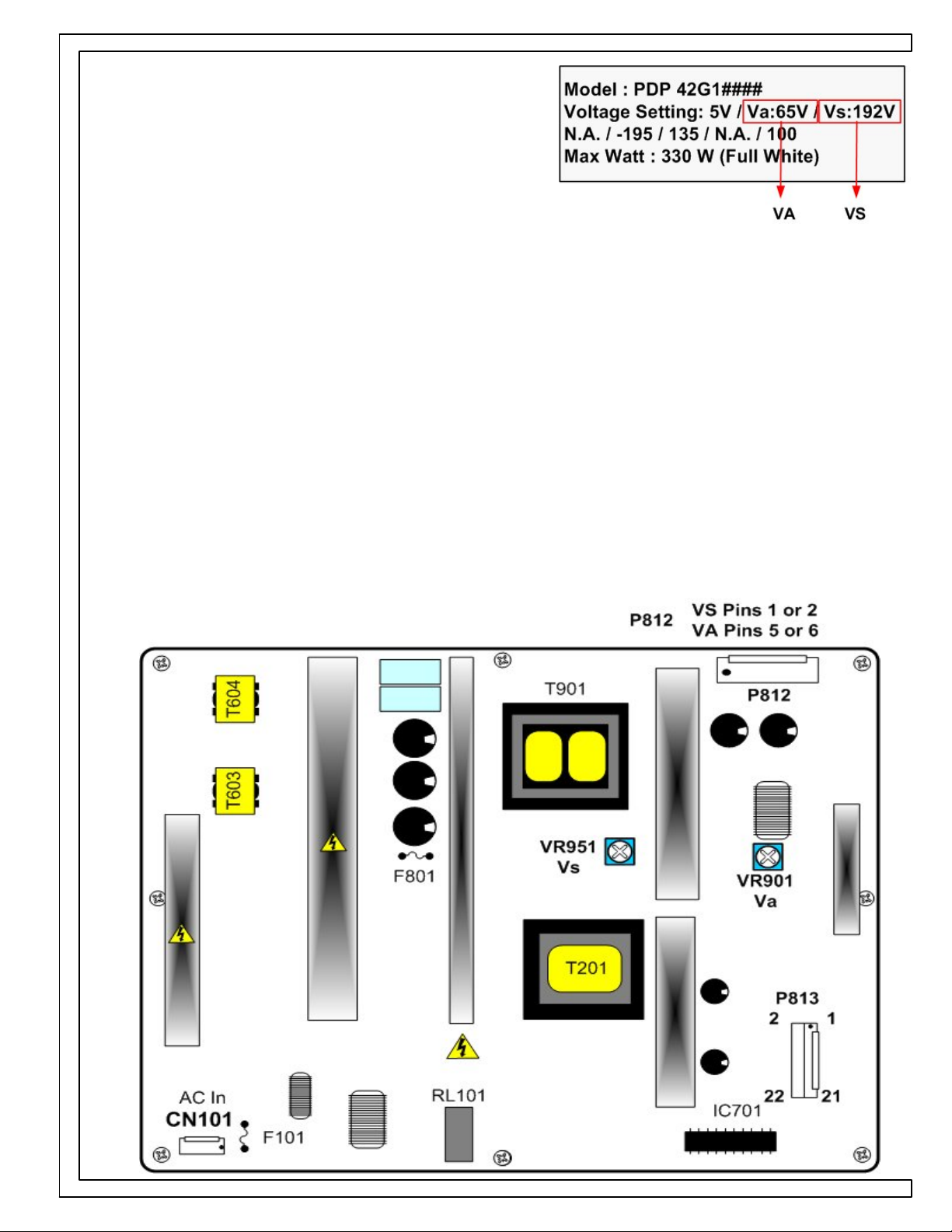
42G1 VS / VA ADJUSTMENT
PREPARATION:
1.) Pre-Heat unit for at least 10
Minutes before making adjustments.
2.) Place unit into White Wash from the Customer’s
Menu for all adjustments.
3.) Be sure to use all adjustment values as
indicated on the panel voltage label in the
upper left hand corner of the panel. (Example above)
PROCEDURE: (See preceding figure for locations)
1.) Adjust VS using VR951. Measured from Pin 1 P812
to chassis ground. Match Panel Voltage label ±1V.
2.) Adjust VA using VR901. Measured from Pin 6 P812
to chassis ground. Match Panel Voltage label ±1V.
42G1 PANEL
Page 12

42G1 Y-SUS BOARD ADJUSTMENT POINTS
V SET DOWN set too high
can cause shut down.
If this happens, remove the LVDS cable and
pre-alighn adjustments.
42G1 PANEL
Page 13

42G1 Y-SUS ADJUSTMENT PREPARATION:
PREPARATION:
1.) Pre-Heat unit for at least 10
Minutes before making adjustments.
2.) Place unit into White Wash from the Customer’s
Menu for all adjustments.
3.) Be sure to use all adjustment values as
indicated on the panel voltage label in the
upper left hand corner of the panel. (Example above)
PROCEDURE: (See figures for locations)
1) Adjust -Vy using VR501. Measured across R210.
Match Panel Voltage label ±1V.
2) Adjust VSC using VR502. Measured across R211
Match Panel Voltage label ±1V.
42G1 PANEL
Voltage Reads Positive
-
-Vy TP R210
+
Lower Left Side
of Board
VR502
VR501
-
VSC TP R211
-Vy Adj
VSC Adj
+
Middle Left Side of Board
Lower Left Side of Board
Page 14

42G1 Y-Drive Waveform Test Point
Figure 1 shows the Y-Drive Waveform Test Point on the Center Top
Y-Drive PWB. Indicated by the Arrow. Use this TP for alignment of the
Y-Drive signal using Set-Up and Set-Down adjustments shown on the
next page.
(Fig. 1)
Y Drive
Waveform TP
Top Y-Drive board.
42G1 PANEL
Page 15
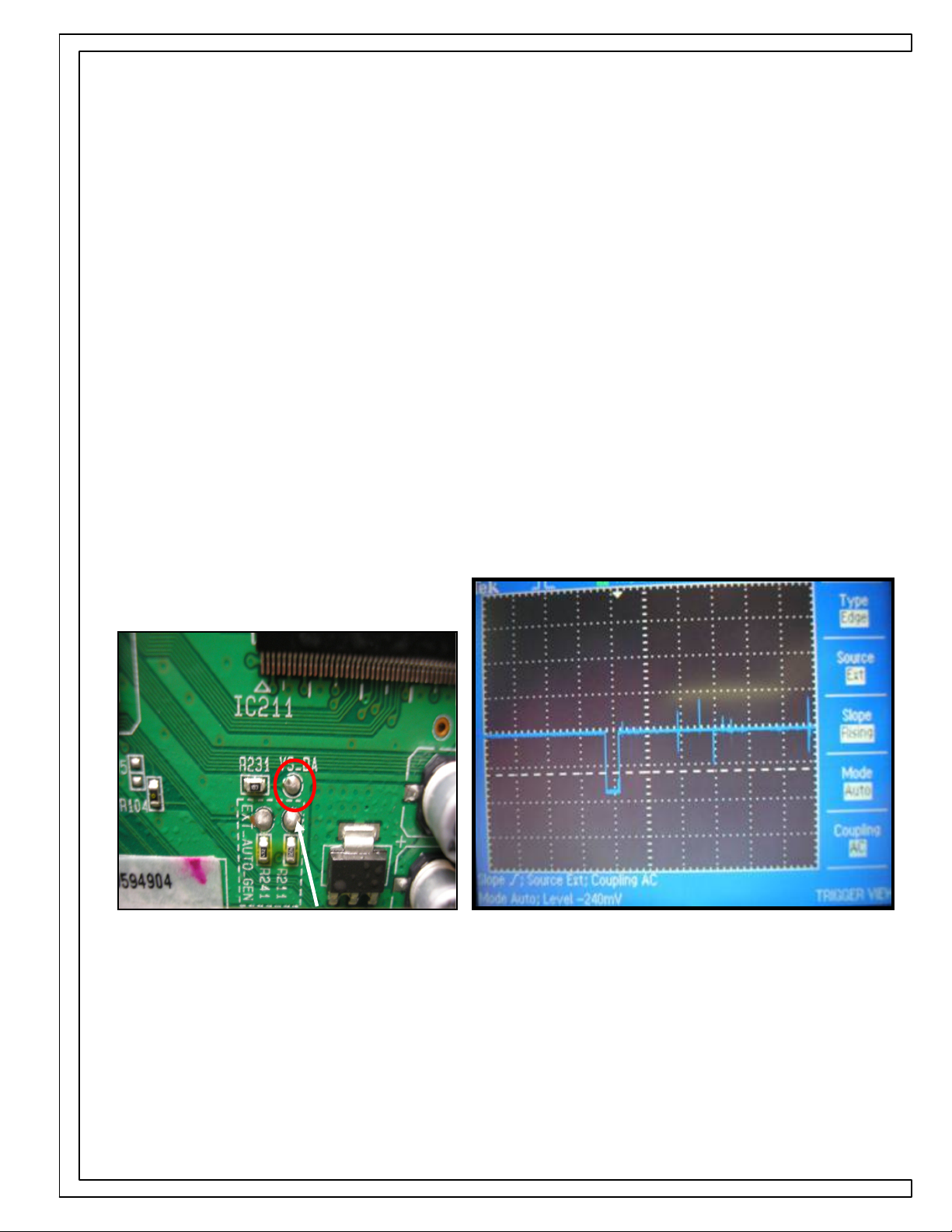
Observing the Y-SUS and Z-SUS Output Waveforms
External Triggering of the Oscilloscope allows for a Stable
Display of both the Y and Z SUS Output Waveforms
regardless of how distorted the waveforms may be,
allowing the wave shape and phasing to be easily
examined.
To set the Oscilloscope up for External Trigger first connect
a Scope Probe set on direct to the External Input Jack.
Next set the External Jack for AC Coupling either positive or
negative slope, use the Trigger Menu on the Scope.
Finally you will need to set the Trigger Level press the
Trigger View and set the level as indicated in the picture
below.
42G1 PANEL
VS_DA Located on the Control Board just above the AUTO
Gen Test Points may be used as an external trigger source
Trigger Level Adjust
for locking the waveform on the Oscilloscope
Page 16

42G1 Y-DRIVE WAVEFORM ADJUSTMENT
PRELIMINARY:
Adjustment locations for adjusting the Y-Drive waveform on the Y-SUS
PWB shown below.
See Y-SUS Test Points and Adjustments diagram for detailed
locations. (4 pages back).
See next page for Adjustment specifications.
Top Left of PWB
Set-Dn
VR401
B
Set-Up
VR601
A
42G1 PANEL
Page 17
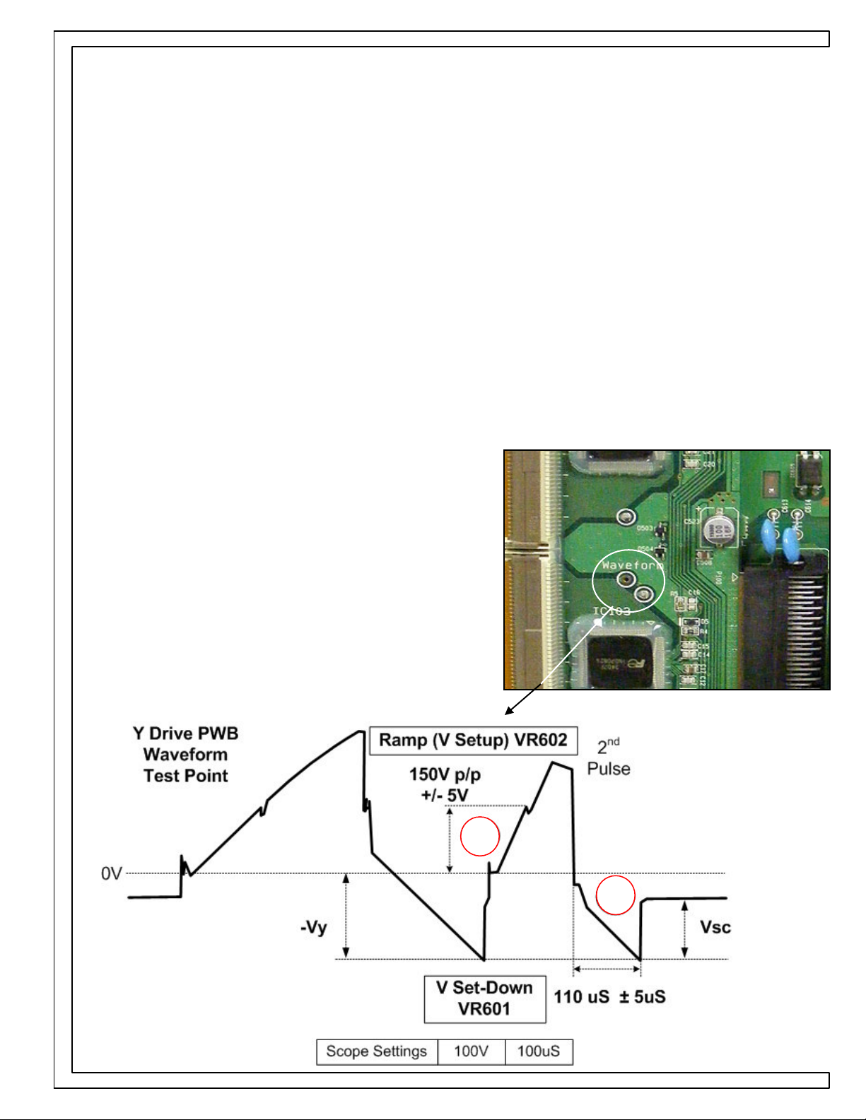
42G1 Y-SUS ADJUSTMENT PREPARATION:
PREPARATION:
1) All adjustment preliminary preparations should be the same as
for Va and Vs adjustments.
2) Va, Vs, -Vy, and VSC adjustments should be complete.
3) Be sure to use all adjustment values as
indicated on the panel voltage label in the upper left hand
corner of the panel.
PROCEDURE: (See preceding page for locations)
Connect scope to Waveform TP on Y-Drive PWB.
1) Adjust RAMP until point “A”in
diagram below is
150V p / p ±5V.
42G1 PANEL
2) Adjust V SET-DOWN until
point “B” in diagram below is
110uSec ±5uS
A
B
Page 18

42G1 Y-SUS BOARD Z-SUS ADJUSTMENT POINTS
Z-Bias Adjustment Section of
the Y-SUS PWB
42G1 PANEL
Page 19

42G1 Z-SUS ADJUSTMENT PREPARATION:
PREPARATION:
1.) Pre-Heat unit for at least 10
Minutes before making adjustments.
2.) Place unit into White Wash from the
Customer’s Menu for all adjustments.
3.) All other adjustments should be complete.
4.) Be sure to use all adjustment values as indicated on the panel
voltage label in the upper left hand corner of the panel.
(Example above)
PROCEDURE: (See preceding page for locations)
1.) Place DC Volt meter on VZB TP (Across R946 on the
Y-SUS Board).
2.) Adjust VZB (Z Bias) VR905 in accordance to your Panel’s
voltage label.
42G1 PANEL
Z-Bias Adj
VR905
+
-
Z-Bias TP
Bottom right side of Y-SUS PWB
R946
Page 20

Intentionally left blank
Page 21

42G2 PLASMA PANEL
42G2 PLASMA PANEL
QUICK REFERENCE
QUICK REFERENCE
ALIGNMENT HAND BOOK
ALIGNMENT HAND BOOK
MODELS USING THE 42G2 PANEL
42PQ20
42PQ30
Page 22

Intentionally left blank
Page 23
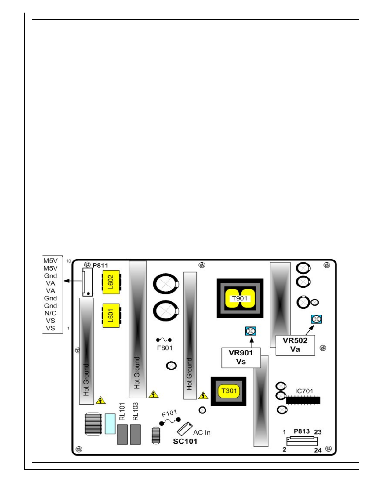
42G2 SMPS BOARD ADJUSTMENT POINTS
These two voltages are adjustable and should be adjusted to the
correct values as indicated by the panel label.
Example shown in the outlined area below.
Always adjust “Highest to Lowest” voltages.
VS and VA adjustment resistors are shown in the drawing below.
They are located towards the top right hand side of the board.
VR901 is the VS adjustment pot.
VR502 is the VA adjustment pot.
Set should be in “Full White Raster”
1) VS ADJUST: Connect DVM to pin 1 or 2 of P811. Adjust VR901 until
the voltage matches the panel’s voltage label.
2) VA ADJUST: Connect DVM to pin 9 or 10 of P811. Adjust VR502 until
the voltage matches the panel’s voltage label.
42G2 PANEL
All measurements taken from Chassis Gnd.
Page 24
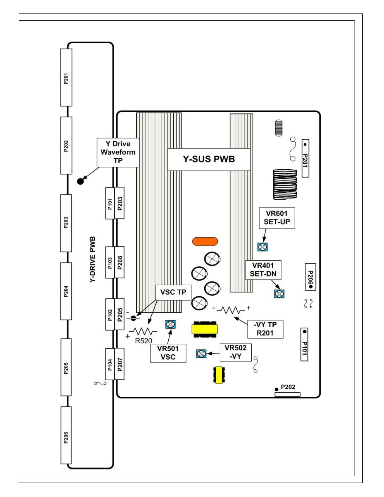
42G2 Y-SUS BOARD ADJUSTMENT POINTS
42G2 PANEL
Page 25
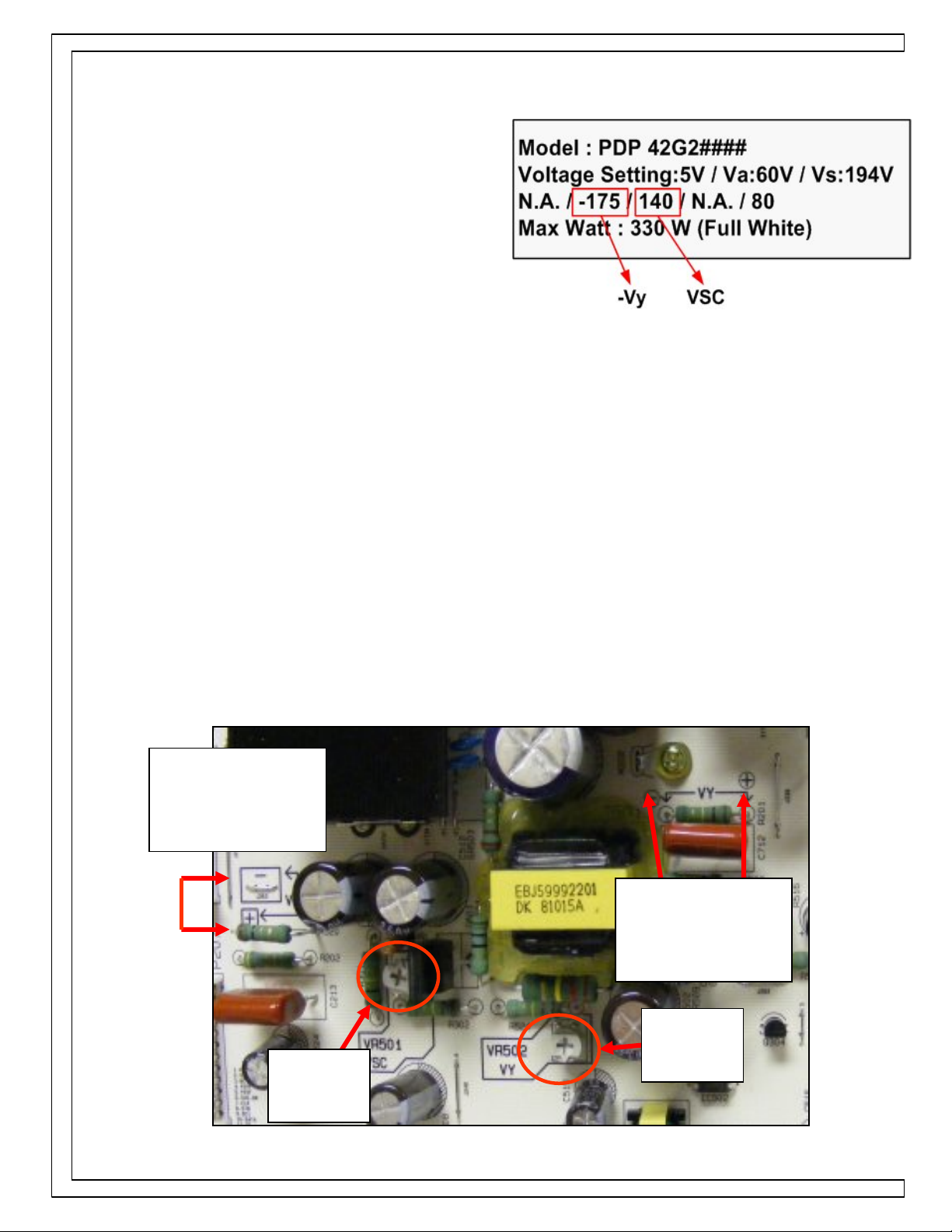
VSC and –Vy Voltage Adjustment Locations
These voltages are adjustable and
Should be adjusted to the correct
values as indicated by the panel’s
voltage label.
Example shown to the right.
-Vy (VR502) variable resistor located bottom center of the board.
Adjust the -Vy (VR502) while reading across R201.
Match your specific panel’s voltage label.
VSC (VR501) variable resistor located bottom center of the board.
42G2 PANEL
Adjust the VSC (VR501) while reading between left side R520 and TP
just above R520. Match your specific panel’s voltage label.
VSC TP
Measure
Across TPs
-Vy TP
Across
VR201
VSC
VR501
-VY
VR502
Page 26

42G2 Y-Drive Waveform Test Point
Figure 1 shows the Y-Drive PWB with the area of the Waveform TP
outlined in the Red circle.
Use this TP for alignment of the Y-Drive signal using Set-Up and SetDown adjustments shown on the next page.
Y-DRIVE
Y Drive
Waveform TP
42G2 PANEL
Y-SUS
(Fig. 1)
Page 27
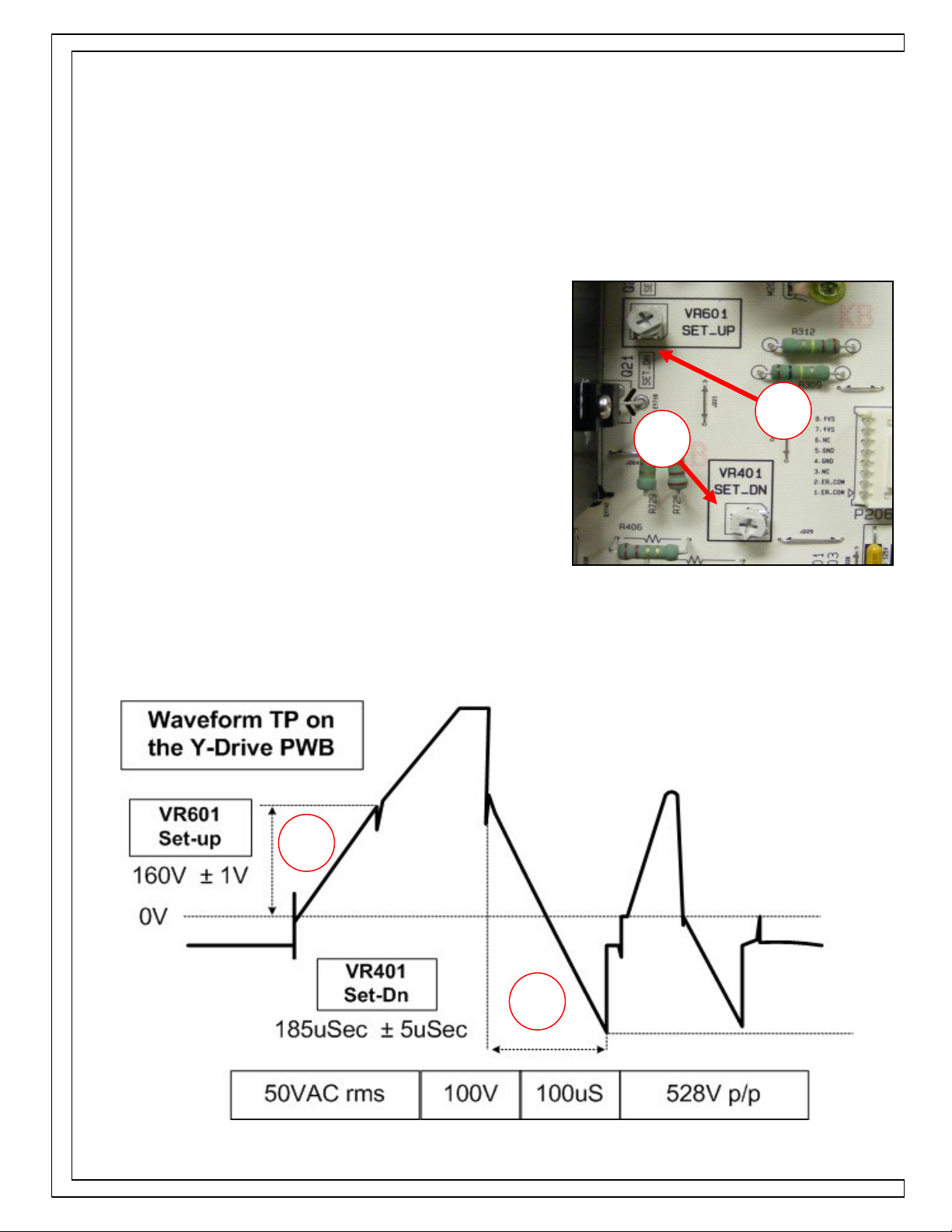
42G2 Y-DRIVE WAVEFORM ADJUSTMENT
VS, VA, VSC, -Vy should have been completed.
See Y-SUS Test
Using a Full White Raster, adjust the
Set-up and Set-dn section of the Y-Drive
waveform.
Oscilloscope TP “Waveform” TP
on the Y-Drive PWB.
(A) Set-Up: Adjust VR601 while observing
area (A) and set to 160V ± 1V.
(B) Set-Down: Adjust VR401 while
observing area (B) and set to
42G2 PANEL
185uSec ± 5uSec.
Points and
Adjustments diagram
for locations.
A
B
A
B
Page 28
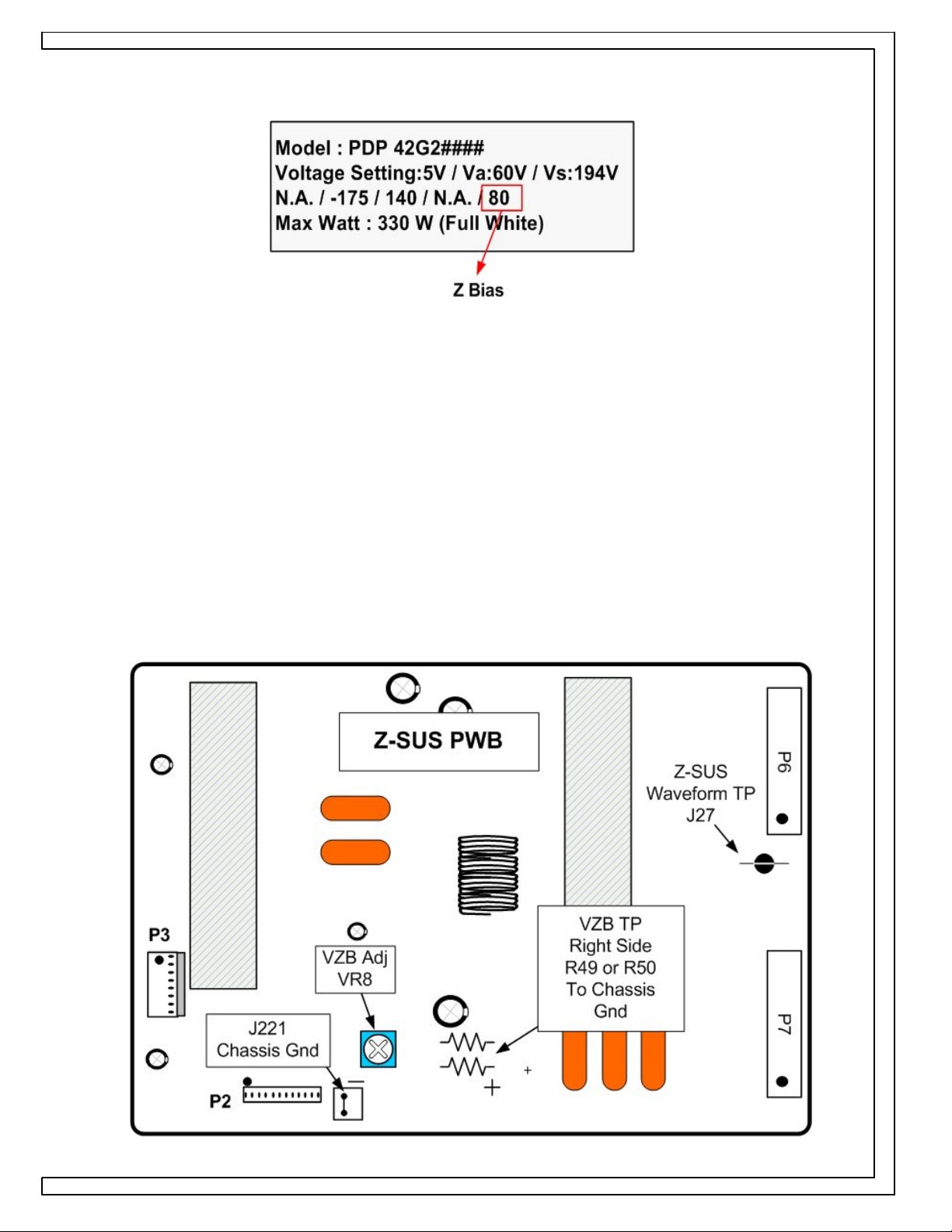
42G2 Z-SUS BOARD ADJUSTMENT POINTS
The above picture represents a 42G2 Panel Voltage Label. This is for an
example only. You should adjust your set’s
Z-Bias adjustment to your specific Panel’s Voltage Label not this book.
The picture below represents the 42G2 Z-SUS PWB. Use this for
reference to locate the Adjustment control and the adjustment Test
Points.
42G2 PANEL
Page 29
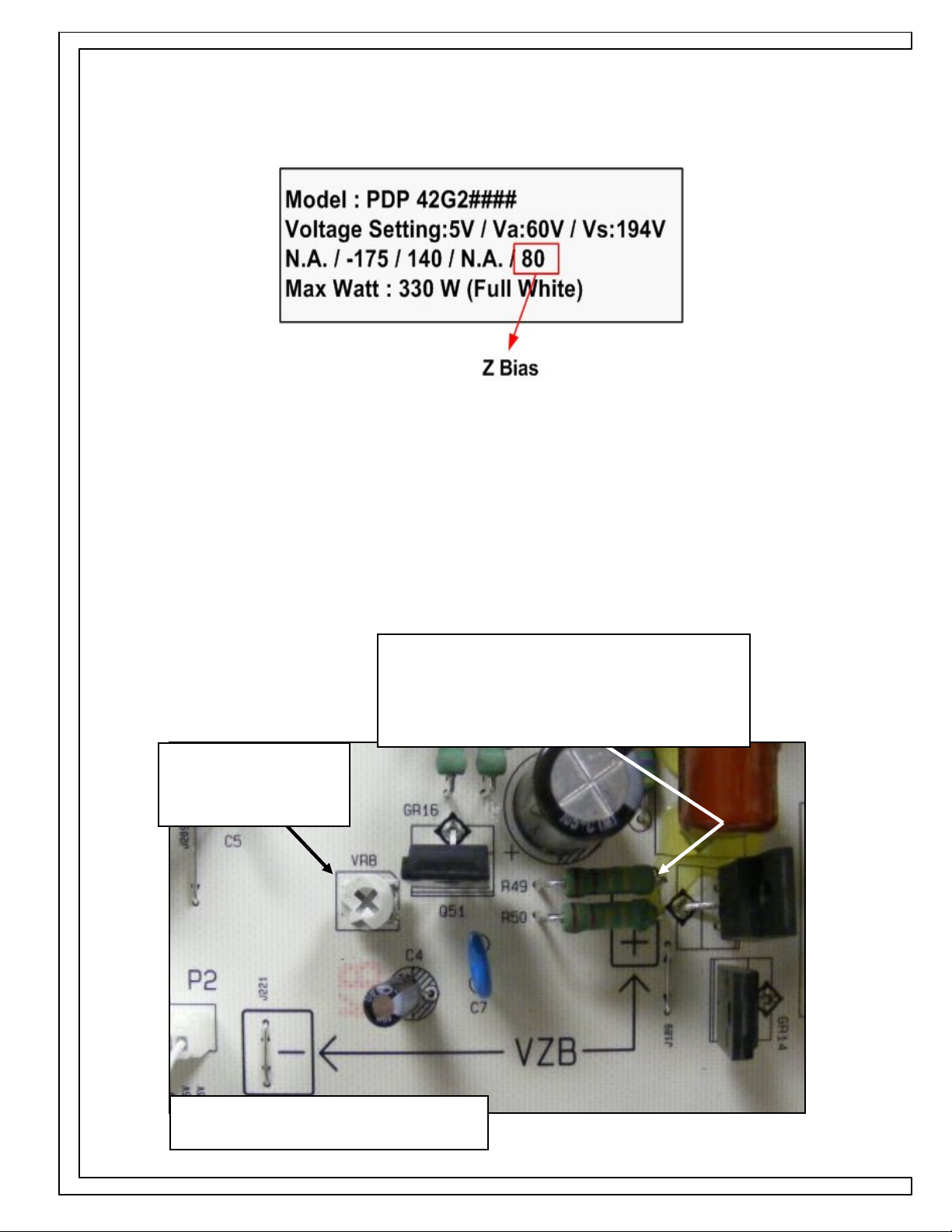
42G2 Z-SUS BOARD ADJUSTMENT POINTS
VS, VA, VSC, -Vy should have been completed.
Full White Raster
1) Z-Bias TP: Connect DVM (+) right side R49 or R50 to
Chassis Gnd.
2) Adjust Z-Bias (VR8) to match your specific panel’s
42G2 PANEL
voltage label.
Z Bias Test Point
Right Side of either R49 or 50
To Chassis Ground
Z Bias Adjust
VR8
Same as Chassis Gnd.
Page 30

Intentionally left blank
Page 31

42T1 PANEL
42T1 PANEL
QUICK REFERENCE
QUICK REFERENCE
ALIGNMENT HAND BOOK
ALIGNMENT HAND BOOK
THE FOLLOWING MODELS USE THE 42T1 PANEL
42PJ350
Page 32

42T1 SMPS BOARD ADJUSTMENT POINTS
Set should be in “White Wash”
These two voltages are adjustable and
should be adjusted to the correct values
as indicated by your Panel’s Voltage
Label. Example shown on the right.
Always adjust “Highest to Lowest” voltages.
VS and VA adjustment resistors are shown in the drawing below.
They are located at the top Right of the board.
1) VS ADJUST:
Connect DVM to VS Test Point or pins 1 or 2 of P811.
Adjust VR901 until the voltage matches your panel’s voltage label.
2) VA ADJUST:
Connect DVM to VA Test Point or pins 6 or 7 of P811.
Adjust VR502 until the voltage matches your panel’s voltage label.
42T1 PANEL
Example: Use Your Panel’s Label
VR502 VR901
Page 33

42T1 Y-SUS BOARD ADJUSTMENT POINTS
42T1 PANEL
Page 34

42T1 VSC, -Vy ADJUSTMENTS
PREPARATION:
1) Pre-Heat unit for at least 10 Minutes
before making adjustments.
Vs and Va adjustments complete.
2) Place unit into White Wash from the
Customer’s Menu for all adjustments.
3) Be sure to use all adjustment values as
indicated on your panel’s voltage label in
the upper left of the panel.
PROCEDURE: (See figure below for locations).
(See previous page for Location details)
Example: Use Your Panel’s Label
1) Adjust –Vy VR502. Measured across –Vy TPs.
Match your specific Panel’s Voltage label ±1V.
2) Adjust VSC VR501. Measured across VSC TPs.
42T1 PANEL
Match your specific Panel’s Voltage label ±1V.
VSC TP
Location: Bottom Left of board
Just below Heat Sink
-
+
VR501
VSC Adj
Voltages Reads Positive
-
-Vy TP
+
VR502
-Vy Adj
Voltages Reads Positive
Location: Bottom Center of board
Just below T501 Transformer
Page 35

42T1 Y Drive Waveform Test Point
The figure below shows a close-up image of the Y-Drive waveform test
point on the Y-Drive Upper board. (Waveform TP).
There is another on the Lower Y-Drive board.
Set-Up and Set-Down portions of the waveform are adjusted using
either of these Test Points.
TP LOCATION UNDER 2ndBUFFER OF Y-DRIVE
(See next page for adjustment Details)
2MSec
Waveform TP
Upper Y-Drive Board
Blanking
Blanking
42T1 PANEL
540V p/p69~72 VRms
100uSec
Page 36

42T1 Y-DRIVE WAVEFORM ADJUSTMENTS
PREPARATION:
1) Pre-Heat unit for at least 10 Minutes before making adjustments.
Vs, Va, -Vy and VSC adjustments should be completed.
2) Place unit into White Wash from the Customer’s Menu for all adjustments.
A
A
42T1 PANEL
See figure below for adjustment locations.
ADJUSTMENT LOCATIONS
(See 3 pages back for Waveform TP locations)
VR601
A
B
VR401
B
B
ADJUSTMENT LOCATION:
Center Right of the board.
SET-UP ADJUST:
1) Adjust VR601 and set the (A) portion of the signal to match the
waveform above. (155V p/p ± 5V)
SET-DN ADJUST:
2) Adjust VR401 and set the (B) time of the signal to match the waveform
above. (170uSec ± 5uSec)
Page 37

42T1 Z-SUS ADJUSTMENT POINTS
42T1 PANEL
Page 38

42T1 Z-SUS (Z-Bias) ADJUSTMENT:
PREPARATION:
1) Pre-Heat unit for at least 10 Minutes
before making adjustments.
2) Place unit into White Wash from the
Customer’s Menu for all adjustments.
3) Be sure to use all adjustment values as indicated
on the panel voltage label in the upper left hand corner of the
panel.
PROCEDURE: (See preceding page for locations)
1. Place DC Volt meter between VZB TPs.
2. Adjust VZB (Z Bias) VR1 in accordance with your Panel’s
voltage label.
Example: Use Your Panel’s Label
VZB (Z Bias)
42T1 PANEL
Location
Bottom Left of Z-SUS Board
-
VZB (Z-Bias)
TP
+
VZB (Z Bias)
VR1
Page 39

42V7 PLASMA PANEL
42V7 PLASMA PANEL
QUICK REFERENCE
QUICK REFERENCE
ALIGNMENT HAND BOOK
ALIGNMENT HAND BOOK
MODELS USING THE 42V7 PANEL
42PC3DVUD
42PM2DS / 2DW
42PM3MVATA / MVHMC / MVMC / MVTA / MVZA
42PM3RV / RV1NC / RVA / RVANC / RVNC / RVS / RVW
42PX3DV / DVA / DVANC / DVAW /
42PX3DVB / DVBNC / DVBW
42PX3DVNC / DVW
42PX3RVMC / RVZA
42PX4DVAZC / DVEA / DW
42PX4MVHTA
42PX4RVHTA / RVMC / RVTA / RVZA
Page 40

Intentionally left blank
Page 41

42V7 SMPS BOARD ADJUSTMENT POINTS
Part Number: 6709V00003A
These two voltages are adjustable and should be adjusted to the
correct values as indicated by the panel label.
Example shown below just above the PWB drawing.
Always adjust “Highest to Lowest” voltages.
VS and VA adjustment resistors are shown in the drawing below.
They are located at the top left of the board.
RV401 is the VS adjustment pot.
RV501 is the VA adjustment pot.
Set should be in “Full White Raster”
1) VS ADJUST: Connect DVM to pin 1, 2 or 3 of P805. Adjust RV401 until
the voltage matches the panel’s voltage label.
2) VA ADJUST: Connect DVM to pin 9 or 10 of P805. Adjust RV501 until
the voltage matches the panel’s voltage label.
42V7 PANEL
Page 42

42V7 SMPS BOARD ADJUSTMENT POINTS
Part Number: EAY32808901
These two voltages are adjustable and should be adjusted to the
correct values as indicated by the panel label.
Example shown below just above the PWB drawing.
Always adjust “Highest to Lowest” voltages.
VS and VA adjustment resistors are shown in the drawing below.
They are located at the top left of the board.
RV401 is the VS adjustment pot.
RV601 is the VA adjustment pot.
Set should be in “Full White Raster”
1) VS ADJUST: Connect DVM to pin 1, 2 or 3 of P805. Adjust RV401 until
the voltage matches the panel’s voltage label.
2) VA ADJUST: Connect DVM to pin 9 or 10 of P805. Adjust RV601 until
the voltage matches the panel’s voltage label.
42V7 PANEL
Page 43

42V7 Y-SUS BOARD ADJUSTMENT POINTS
42V7 PANEL
Page 44

VSC and –Vy Voltage Adjustment Locations
These voltages are
Adjustable and should
be adjusted to the
correct values as
indicated by the panel’s
voltage label.
Example shown in the top right.
VSC (VR3) adjustment resistor located top center of the board is
shown in the picture below.
Adjust the VSC (VR3) while reading across R53 until voltage matches
the panel’s voltage label.
-Vy (VR4) adjustment resistor located top center of the board is
shown in the picture below.
Adjust the -Vy (VR4) while reading across R78 until voltage matches
the panel’s voltage label.
-VSC
TP
R53
-VY
VSC
VR3
-VY
VR4
42V7 PANEL
TP
R78
Page 45

42V7 Y-Drive Waveform Test Point
Figure 1 shows the Y-SUS PWB with the area of the Waveform TP
outlined in the white box.
Figure 2
Shows a close-up image of the Y-Drive waveform test point B32.
42V7 PANEL
B32
(Fig. 2)
(Fig. 1)
Lower Left Hand Side
of the Y-SUS PWB
Page 46

42V7 Y-DRIVE WAVEFORM ADJUSTMENT
VS, VA, VSC, -Vy should have been completed.
See Y-SUS Test
Using a Full White Raster, adjust the Setup and Set-dn section of the Y-Drive
waveform.
Oscilloscope TP B32 on the “Waveform”
TP on the Y-SUS PWB.
(A) Set-Up: Adjust VR1 while observing
area (A) and set to
10uSec ± 1uSec.
(B) Set-Down: Adjust VR2 while
observing area (B) and set to
100uSec ± 1uSec.
Points and
Adjustments diagram
for locations.
B
Set-Down
A
Set-Up
A
B
After adjustment, please recheck VS, VA, VSC, -Vy and Z-bias.
42V7 PANEL
Page 47

42V7 Z-SUS BOARD ADJUSTMENT POINTS
42V7 PANEL
Page 48

42V7 Z-SUS PWB ADJUSTMENT POINTS
VS, VA, VSC, -Vy should have been completed.
Full White Raster
1) Z-Bias TP: Connect DVM across R23.
2) Adjust Z-Bias (VR1) to match the panel’s voltage label.
Z Bias Test Point
Across R23
Bottom of the Y-SUS Board
42V7 PANEL
Z Bias Adjust
VR1
Page 49

42X2 and 42X2A PANEL
42X2 and 42X2A PANEL
QUICK REFERENCE
QUICK REFERENCE
ALIGNMENT SECTION
ALIGNMENT SECTION
THE FOLLOWING MODELS
USE THE 42X2 PANEL
DN42PX12X
DN42PX13X
DN42PX13XW
DN42PX40X
DN42PY10X
DN42PY11X
DN42PY11X
DN42PZ66
DN42PZ75
DT42PY10X
MZ42PM12X
MZ42PZ92XV
RP42PY10X
RT42PX12X
RT42PY10X
RZ42PX12X
RZ42PY10X
THE FOLLOWING MODELS
USE THE 42X2A PANEL
42PM2D
42PX2DUC
42PX4DGS
42PX4DGS2
42PX4DGW
42PX4DNA
42PX4DR
42PX4DR
42PX4DRK
42PX4DRKNA
42PX5D
42PX5DEB
42PX5RTB
DN42PX12
DU42PX12X
DU42PY10X
MN42PZ95XV
MU42PM12X
MU42PZ90XV
42PX4DRKS
42PX4DRKW
42PX4DRW
42PX4DS
42PX4DUB
Page 50

42X2 SMPS BOARD ADJUSTMENT POINTS
Set should be in “White Wash”
These voltages are adjustable and should be adjusted to
the correct values as indicated by your Panel’s Voltage
Label. Examples shown on the right.
Always adjust “Highest to Lowest” voltages.
Adjustment resistors are shown in the drawing below.
They are located at the top Right of the board.
Note: Your Board my vary in appearance.
1) 3.4V ADJUST:
Connect DVM to Pin 1 or 2 of P802
Adjust VR251 (3.4V Adj) until the DVM reads 3.4V
2) 6V ADJUST:
Connect DVM to Pin 5 or 6 of P802
Adjust VR280 (6V Adj) until the DVM reads 6V
3) 5V ADJUST:
Connect DVM to Pin 3 of P801
Adjust VR159 (5V Adj) until the DVM reads 5V
42X2 PANEL
4) 19V ADJUST: (Audio)
Connect DVM to Pin 1 or 2 of P803
Adjust (19V Adj) pot until the DVM reads 19V
VA
VR551
The Label difference between
a 42X2 and 42X2##2#
5) VS ADJUST:
Connect DVM to Pin 9 or 10 of P805
Adjust VR551 and match your label.
6) VA ADJUST:
Connect DVM to Pin 1 or 2 of P803
Adjust VR351 (VS Adj) and match your label
VS
VR901
VR159
5V
Page 51

42X2 Y-SUS BOARD ADJUSTMENT POINTS
42X2 PANEL
Page 52

42X2 VSCAN and -Vy ADJUSTMENTS
PREPARATION:
1) Pre-Heat unit for at least 10 Minutes
before making adjustments.
Vs and Va adjustments complete.
2) Place unit into White Wash from the
Customer’s Menu for all adjustments.
3) Be sure to use all adjustment values as indicated on your panel’s voltage label
in the upper left of the panel.
PROCEDURE: (See figure below for locations)
1) Adjust –Vy (VR On PS101). Measured across –Vy TP R117.
Match your specific Panel’s Voltage label ±1V.
2) Adjust Vscan (VR On PS102). Measured across Vscan TP C142.
Match your specific Panel’s Voltage label ±1V.
Location: Bottom Left of board
-Vy VSC
42X2 PANEL
Voltage Reads
Positive
For Vscan Adj.
You can clip the
black lead of the
DVM to either of
these two screws
going to the
Y-Drive
PS102
+
VScan
Adj
-
For -Vy Adj.
C142
VScan TP
-Vy
Adj
PS101
+
You can clip the
black lead of the
DVM to the
bottom leg of
R118 just to the
left of R117.
Voltage Reads
Positive
R117
-Vy TP
-
Page 53

42X2 Y-SUS Drive Waveform Test Point
The figure below shows a close-up image of the Y-Drive waveform test point on
the Y-SUS board. (B1).
It is located on the Center Left hand side of the Y-SUS board.
VRamp, VSet-Up and VSet-Down portions of the waveform are adjusted using this
Test Point.
TP LOCATION UNDER CENTER SET OF TWO SCREWS TO THE
Y-DRIVE BOARD (See next page for adjustment details)
2MSec
Waveform TP B1
Center Left of the Board
Blanking
42X2 PANEL
Page 54

42X2 Y-DRIVE WAVEFORM ADJUSTMENTS
PREPARATION:
1) Pre-Heat unit for at least 10 Minutes before making adjustments.
All DC adjustments to the panel should have been completed.
2) Place unit into White Wash from the Customer’s Menu for all adjustments.
ADJUSTMENT LOCATIONS
(See 3 pages back for Adjustment VR and Waveform TP locations)
VRAMP ADJUST:
1) Adjust VR51 and set the (A) time of the signal to match the
waveform shown below. (10uSec ± 2uSec)
VR51
A
B
42X2 PANEL
VR22
VR11
VSET-UP ADJUST:
2) Adjust VR22 and set the (B) portion of the signal to match
the waveform shown below.
42X2#### panel (100V ± 10V) or
42X2##2# panel (80V ± 10V)
Waveform Test Point
Y-SUS Center Left (Waveform TP B1)
C
ADJUSTMENT
LOCATIONS:
Bottom Center of
the board.
VSET-DN ADJUST:
2) Adjust VR11 and set the (C) time of the signal
to match the waveform shown above.
(20uSec ± 5uSec)
Page 55

42X2 Z-SUS ADJUSTMENT POINTS
42X2 PANEL
p/n 6781QZH034C
Page 56

42X2 Z-SUS (Z-Bias) ADJUSTMENT:
PREPARATION:
1) Pre-Heat unit for at least 10 Minutes before
making adjustments.
2) Place unit into White Wash from the
Customer’s Menu for all adjustments.
3) Be sure to use all adjustment values as indicated on the panel voltage
label in the upper right hand corner of the panel.
PROCEDURE: (See preceding page for locations)
1. Place DC Volt meter on VZB TP (Across R111). Top side to Chassis
Ground.
2. Adjust VZB (Z Bias) pot located on PS101 in accordance with your
Panel’s voltage label.
Top Right of Z-SUS Board
VZB (Z Bias)
PS101
42X2 PANEL
VZB (Z Bias)
VZB (Z-Bias) TP
Top Side R111
Page 57

42X3 PLASMA PANEL
42X3 PLASMA PANEL
QUICK REFERENCE
QUICK REFERENCE
ALIGNMENT HAND BOOK
ALIGNMENT HAND BOOK
MODELS USING THE 42X3 PANEL
42PB2DR / DR1 / DRNA / DR1S / DRD
42PB2DRL/ DRLNA / DRNA/ DRW
42PB2RR / B2RRML
42PC1D / D1 / D1ND / D1NF / D1S / D1W / D1DA
42PC1DB / DB1 / DB1ND / DB1NF / DB1S / DB1S1 / DB1W
42PC1DBND/ DCNF / DDA / DND / DR / DR1 / DR1NA / DR1W
42PC1DR2 / DR2NA/ DRA / DRANA / DRNA / DRW / DRW1
42PC1DRWNA / DRX / DRXNA / DW / RRTL / RRZL / RTH / RZH
42PC3D / DHUD / DUD / RAZJ
42PC7DHUA / RHMA
42PM2DNA
42PX3DUE
42PX4D / DAA / DG / DGNB / DNB / DRB / DRBNA / DRBS
42PX4DRBW / DRBW1 / DRBW2 / DRNA / DRNA
42PX5DA / DA1 / DA1NA / DANA / DAW / DMNA / DNA
Page 58

Intentionally left blank
Page 59

42X3 SMPS Test Points and Adjustments
42X3 PANEL
Page 60

42X3 VA and VS Voltage Adjustment Locations
These two voltages are adjustable
and should be adjusted to the
correct values as indicated by the
panel label.
Example shown in the top right.
Always adjust “Highest to Lowest”
voltages.
VS and VA adjustment resistors are shown in the picture below.
They are located at the top left of the board.
VR901 is the VS adjustment pot.
VR951 is the VA adjustment pot.
Set should be in “Full White Raster”
1) VS ADJUST: Connect DVM to pin 8 or 9 of P812. Adjust VR951
until the voltage matches the panel’s voltage label.
2) VA ADJUST: Connect DVM to pin 6 of P812. Adjust VR901 until
the voltage matches the panel’s voltage label.
42X3 PANEL
Top Left of the SMPS PWB
Page 61

42X3 Y-SUS Test Points and Adjustment Locations
42X3 PANEL
Page 62

42X3 VSC and –Vy Voltage Adjustment Locations
These two voltages are adjustable
and should be adjusted to the
correct values as indicated by the
panel label.
(Upper left hand side of the Panel).
Example shown in the top right.
Always adjust “Highest to Lowest”
voltages.
-Vy and VSC adjustment resistors
are shown in the picture below.
They are located on the Boards labeled PS101 and S102.
PS101 is the -VY supply
PS102 is the VSC supply
Adjust the –Vy adjustment pot on the PS101 module while reading
across R36 until voltage matches the panel’s voltage label. (See
previous page for location).
Adjust the VSC adjustment pot on the PS102 module while reading
across C51 until voltage matches label. (See previous page for
location).
VSC Adj
PS102
PS101
-VY Adj
42X3 PANEL
Page 63

42X3 Y Drive Waveform Test Point
Figure 1 shows the Y-Drive Board
Figure 2
Shows a close-up image of the Y-Drive waveform
test point.
42X3 PANEL
(Fig. 1)
(Fig. 2)
Page 64

42X3 Y-Drive Waveform Adjustment
Using a Full White Raster, adjust the
Set-up and Set-dn section of the Y-Drive
waveform. VS, VA, -Vy and VSC should
have been completed.
Oscilloscope TP on the “Waveform” TP on
See Y-SUS Test
Points and
Adjustments diagram
for locations.
the Y-Drive PWB.
V Set-Up Adjustment: Adjust VR3 while
observing area (A) and set to 150V ± 1V.
V Set-Down Adjustment: Adjust VR2 while
observing area (B) and set to 10uSec ±
5uSec.
A
A
B
42X3 PANEL
B
Page 65

Z-SUS Test Points and Adjustment Locations
42X3 PANEL
Page 66

Z-SUS (Z-Bias Adjustment)
All other adjustments should have been completed.
Full White Raster
Z-Bias Adjustment:
Adjust Z-Bias while reading the voltage between Q18 Collector to
chassis ground. Match your specific panel’s Voltage Label.
PS101
Z-Bias
Adjustment
Bottom Center of the SMPS Board
42X3 PANEL
Measure VZBias from collector of
Q18 to ground.
Page 67

42X4A PANEL
42X4A PANEL
QUICK REFERENCE
QUICK REFERENCE
ALIGNMENT SECTION
ALIGNMENT SECTION
MODELS USING THE 42X4A PANEL
42PB2RRHML
42PB4D / DAA / DAUA / DNB / DR /
42PB4D DRNA / DRPNG / DTUB
42PB4RTMA / RTTB
42PC1D2 / D2NF / DB2 / DB2NF / DGAA
42PC35ZC
42PC3DA / DANA / DANG
42PC51ZB
42PC5D / DAB / DCNB / DDB / DNA / DNG / DUC / DUL /
DZB
42PC5RHTB / RTB / RZB
42PC7RAMA
42PT81ZB
Page 68

Intentionally left blank
Page 69

42X4A SMPS PWB ADJUSTMENT POINTS
These two voltages are adjustable and should be adjusted to the
correct values as indicated by the panel label.
Example shown in the outlined area below.
Always adjust “Highest to Lowest” voltages.
VS and VA adjustment resistors are shown in the drawing below.
They are located at the top left of the board.
VR901 is the VS adjustment pot.
VR951 is the VA adjustment pot.
Set should be in “Full White Raster”
1) VS ADJUST: Connect DVM to pin 7 or 8 of P12. Adjust VR901 until the
voltage matches the panel’s voltage label.
2) VA ADJUST: Connect DVM to pin 3 of P12. Adjust VR951 until the
voltage matches the panel’s voltage label.
42X4 PANEL
Page 70

42X4A SMPS PWB ADJUSTMENT POINTS
These two voltages are adjustable and should be adjusted to the
correct values as indicated by the panel label.
Example shown in the outlined area below.
Always adjust “Highest to Lowest” voltages.
VS and VA adjustment resistors are shown in the drawing below.
They are located at the top left of the board.
VR951 is the VS adjustment pot.
VR901 is the VA adjustment pot.
Set should be in “Full White Raster”
1) VS ADJUST: Connect DVM to pin 8 or 9 of P812. Adjust VR951 until
the voltage matches the panel’s voltage label.
2) VA ADJUST: Connect DVM to pin 3 of P812. Adjust VR901 until the
voltage matches the panel’s voltage label.
42X4 PANEL
Page 71

42X4A Y-SUS PWB ADJUSTMENT POINTS
42X4 PANEL
Page 72

42X4 –Vy Voltage Adjustment Locations
-VY
The -Vy voltages is adjustable
and should be adjusted to the
correct values as indicated by the panel label.
Example shown in the top right.
-Vy adjustment resistor R65
is shown in the picture below.
They are located bottom left of the board.
Adjust the -Vy (VR4) while reading across R65 until voltage matches
label. (See previous page for location).
-VY
VR4
-VY
42X4 PANEL
TP
R65
Page 73

42X4 Y Drive Waveform Test Point
Figure 1 shows the Y-Drive Board
Figure 2
Shows a close-up image of the Y-Drive
waveform test point.
42X4 PANEL
(Fig. 2)
(Fig. 1)
Page 74

42X4 Y-Drive Waveform Adjustment
Using a Full White Raster, adjust the
Set-up and Set-dn section of the Y-Drive
waveform. VS, VA, -Vy and VSC should
have been completed.
Oscilloscope TP on the “Waveform”
TP on the Y-Drive Board.
1) Set-Up: Adjust VR3 while
observing area (A) and set to
305V ± 1V.
2) Set-Down: Adjust VR2 while
observing area (B) and set to
120uSec ± 5uSec.
See Y-SUS Test
Points and
Adjustments diagram
for locations.
A
A
B
42X4 PANEL
B
Page 75

42X4A Z-SUS BOARD ADJUSTMENT POINTS
42X4 PANEL
Page 76

42X4A Z-SUS BOARD ADJUSTMENT POINTS
All other adjustments should have been completed.
Full White Raster
1) Connect DVM between Q2 Drain and chassis ground
2) Adjust Z-Bias (VR1) to match the panel’s voltage label.
Lower Right Hand Side of PWB
VR1
Z Bias Adjust
Z Bias Test Point
Q2 Drain
42X4 PANEL
Chassis Gnd
Measure Vzbias from Drain
of Q2 to Chassis Ground.
Page 77

50G1 PLASMA PANEL
50G1 PLASMA PANEL
QUICK REFERENCE
QUICK REFERENCE
ALIGNMENT HAND BOOK
ALIGNMENT HAND BOOK
MODEL USING THE 50G1 PANEL
50PG20
Page 78

Intentionally left blank
Page 79

50G1 Vs / Va ADJUSTMENT
PREPARATION:
1) Pre-Heat unit for at least 10
Minutes before making
adjustments.
2) Place unit into White Wash from the
Customer’s Menu for all adjustments.
3) Be sure to use all adjustment values as
indicated on the panel voltage label in the
upper left hand corner of the panel. See example above.
PROCEDURE: (See figure for locations)
1) Adjust Vs using VR901. Measured from Pin 1 or 2 P801 to
chassis ground. Match Panel Voltage label ±1V.
2) Adjust Va using VR902. Measured from Pin 5 or 6 P801 to
chassis ground. Match Panel Voltage label ±1V.
50G1 PANEL
Page 80

50G1 Y-SUS BOARD ADJUSTMENT POINTS
50G1 PANEL
Page 81

50G1 -Vy / VSC ADJUSTMENT
PREPARATION:
1) Pre-Heat unit for at least 10 Minutes
before making adjustments.
2) Place unit into White Wash from the
Customer’s Menu for all adjustments.
3) Be sure to use all adjustment values as indicated on the
panel voltage label in the upper left hand corner of the
panel. See example to the upper right.
PROCEDURE: (See previous page for locations)
1) Adjust -Vy using VR501. Measured across R201.
Match Panel Voltage label ±1V.
2) Adjust VSC using VR502. Measured across R202.
Match Panel Voltage label ±1V.
50G1 PANEL
VSC
ADJ
VR502
- +
Upper Left Side Of PWB
-VY ADJ
VR501
Lower Left Side of Board
+
-
Lower Left Side Of Board
Page 82

50G1 Y Drive Waveform Test Point
Figure 1 shows the Y-Drive Waveform Test Point on the Y-Drive
PWB. Indicated by the Arrow. There are several test points that
can be used, but they are not marked. Look just above and
below each output buffer. Three of the heat sinks will have test
points just like the one below.
Use this TP for alignment of the Y-Drive signal using Set-Up
and Set-Down adjustments shown on the next page.
(Fig. 1)
Y Drive
Waveform TP
Bottom of the Y-Drive board.
50G1 PANEL
Page 83

Observing the Y-SUS and Z-SUS Output Waveforms
External Triggering of the Oscilloscope allows for a Stable
Display of both the Y and Z SUS Output Waveforms
regardless of how distorted the waveforms may be,
allowing the wave shape and phasing to be easily
examined.
To set the Oscilloscope up for External Trigger first connect
a Scope Probe set on direct to the External Input Jack.
Next set the External Jack for AC Coupling either positive or
negative slope, use the Trigger Menu on the Scope.
Finally you will need to set the Trigger Level press the
Trigger View and set the level as indicated in the picture
below.
50G1 PANEL
VS_DA Located on the Control Board just above the AUTO
Gen Test Points may be used as an external trigger source
Trigger Level Adjust
for locking the waveform on the Oscilloscope
Page 84

50G1 Y-DRIVE WAVEFORM ADJUSTMENT
PRELIMINARY:
Adjustment locations for adjusting the Y-Drive waveform on the
Y-SUS PWB shown below.
See Y-SUS Test Points and Adjustments diagram for detailed
locations. (4 pages back).
See next page for Adjustment specifications.
Right Center Top of PWB
Upper Left of PWB
50G1 PANEL
Set-Up
VR601
A
Set-Dn
VR401
B
Page 85

50G1 Y-SUS ADJUSTMENT PREPARATION:
PREPARATION:
*Be sure to use all adjustment values as indicated on the
panel voltage label in the upper left hand corner of the panel.
NOTE
the Y-Drive waveform.
Connect scope to Waveform TP. (Shown 3 pages back)
PROCEDURE:
(See preceding page for adjustment locations)
1) SET-UP: Adjust SET-UP VR601 until point “A” in
diagram below is 150V pp ± 5V
2) Set-DOWN: Adjust SET-DOWN until point “B” in
diagram below is 100uSec ±5uS.
50G1 PANEL
: All DC adjustments must be corrected prior to Adjustment of
If V-Set-Dn exceeds 120us the unit will shut down.
If this occurs remove LVDS cable and readjust V-Set-Dn.
Page 86

50G1 Z-SUS BOARD ADJUSTMENT POINTS
For Z-Waveform, attach scope to Z-SUS TP.
Any bottom leg of any capacitor on the Z-SUB board.
Be care, these legs are close together.
50G1 PANEL
Page 87

50G1 Zbias ADJUSTMENT
PREPARATION:
1) Pre-Heat unit for at least
10 Minutes before making
adjustments.
2) Place unit into White Wash from the
Customer’s Menu for all adjustments.
3) Be sure to use all adjustment values as
indicated on the panel voltage label in the
upper left hand corner of the panel. See example above.
PROCEDURE: (See figures for locations)
1) Adjust Zbias using VR8. Measured from the bottom side
of R49 or R50 to chassis ground.
Match Panel Voltage label ±1V.
50G1 PANEL
Z Bias Adj
VR8
Z Bias TP
Bottom of
R49 or R50
To Chassis Gnd.
Top Side Of Board
Page 88

Intentionally left blank
Page 89

50G2 PLASMA PANEL
50G2 PLASMA PANEL
QUICK REFERENCE
QUICK REFERENCE
ALIGNMENT HAND BOOK
ALIGNMENT HAND BOOK
MODEL USING THE 50G2 PANEL
50PQ20
50PQ30
Page 90

Intentionally left blank
Page 91

50G2 Vs / Va ADJUSTMENT
PREPARATION:
1) Pre-Heat unit for at least 10
Minutes before making
adjustments.
2) Place unit into White Wash from the
Customer’s Menu for all adjustments.
3) Be sure to use all adjustment values as
indicated on the panel voltage label in the
upper left hand corner of the panel. See example above.
PROCEDURE: (See figure for locations)
1) Adjust Vs using VR901. Measured from Pin 1 or 2 P811 to
chassis ground. Match Panel Voltage label ±1V.
2) Adjust Va using VR502. Measured from Pin 6 or 7 P811 to
chassis ground. Match Panel Voltage label ±1V.
50G2 PANEL
Page 92

50G2 Y-SUS BOARD ADJUSTMENT POINTS
50G2 PANEL
Page 93

50G2 -Vy / VSC ADJUSTMENT
PREPARATION:
1) Pre-Heat unit for at least 10 Minutes
before making adjustments.
2) Place unit into White Wash from the
Customer’s Menu for all adjustments.
3) Be sure to use all adjustment values as indicated on the
panel voltage label in the upper left hand corner of the
panel. See example to the upper right.
PROCEDURE: (See previous page for locations)
1) Adjust -Vy using VR502. Measured across R201.
Match Panel Voltage label ±1V.
50G2 PANEL
2) Adjust VSC using VR501. Measured across R202.
Match Panel Voltage label ±1V.
Lower portion of the board
Page 94

50G2 Y Drive Waveform Test Point
The Figure below shows the Y-Drive Waveform Test Points on the Y-Drive boards.
Indicated by the circles. There are several test points that can be used, but they
are not marked. Look just above and below each output buffer.
Use this TP for alignment of the Y-Drive signal using Set-Up and Set-Down
adjustments shown on the next page.
(Fig. 1)
There are several other test points on either the Upper or Lower Y-Drive
boards that can be used.
Basically any output pin on any of the FPC to the panel are OK to use.
Y-Drive Upper Test
Point
(Bottom of Board)
VR108
VR209
Y-Drive Lower Test
Point
(Top of Board)
c Overall signal observed
d Highlighted signal from
waveform above observed
e Highlighted signal
from waveforms
above observed
100uS/div
4mS/div
400uS/div
80VRms
50G2 PANEL
516V p/p
NOTE: The Waveform Test Points are
fragile. If by accident the land is torn and
the run lifted, make sure there are no lines
left to right in the screen picture.
100uS
Page 95

Observing the Y-SUS and/or Z-SUS Output Waveforms
External Triggering of the Oscilloscope allows for a Stable Display of both the
Y-SUS and Z SUS Output Waveforms. Regardless of how distorted the
waveforms may be, using this TP will assist in locking the scope, allowing the
wave shape and phasing to be easily examined.
To set the Oscilloscope up for External Trigger first connect a Scope Probe set on
direct to the External Input Jack.
Next set the External Jack for AC Coupling either positive or negative slope, use the
Trigger Menu on the Scope.
Finally you will need to set the Trigger Level press the Trigger View and set the
level as indicated in the picture below.
50G2 PANEL
Trigger Level Adjust
VS_DA Located on the Control Board just above the AUTO
Gen Test Points. This TP may be used as an external trigger source for locking
the waveform on the Oscilloscope
Page 96

50G2 Y-DRIVE WAVEFORM ADJUSTMENT
PRELIMINARY: Set must be in “WHITE WASH”
All other DC Voltage adjustments should have already been made.
Adjustment locations for adjusting the Y-Drive waveform are on the Y-SUS board.
See Y-SUS Test Points and Adjustments diagram for detailed locations.
(4 pages back).
SET-UP ADJUST:
1) Adjust VR601 and set the (A) portion of the signal to match the
waveform below. (150V ± 5V)
SET-DN ADJUST:
2) Adjust VR401 and set the (B) time of the signal to match the
waveform below. (150uSec 5uSec)
VR601
VR401
ADJUSTMENT LOCATIONS:
Top Left VR601.
Center Right VR401
50G2 PANEL
Page 97

50G2 Z-SUS BOARD ADJUSTMENT POINTS
P101
Z-Bias TP
Top of R271 or R272
To Chassis Ground
50G2 PANEL
FS100
M5V
FS100
M5V
FS102
Vs
P104
FPC
Z-Bias
VR200
Z-SUS
Waveform
Test Point
J27
P100
FS101
17V
P105
FPC
P103
Page 98

50G2 Z-SUS Z BIAS (VZB) ADJUSTMENT
PRELIMINARY: Set must be in “WHITE WASH”
All other DC Voltage adjustments should have already been made.
Note: You can also measure across
C239 for the VZB (Zbias) adjustment.
Read the Label on the back of the upper left hand
side of the panel when adjusting VR200.
Top of Z-SUS
Board
Chassis Ground or the
Top of C239 or J125
VZB (Z-Bias) TP Top
Side R271 or R272
VZB (Z Bias)
VR200
Z Bias
50G2 PANEL
Adjustment:
VZ (Z-Bias) to match your specific Panel’s Voltage Label (± 1V)
Measured from Chassis Ground
Page 99

50H1 PLASMA PANEL
50H1 PLASMA PANEL
QUICK REFERENCE
QUICK REFERENCE
ALIGNMENT HAND BOOK
ALIGNMENT HAND BOOK
MODELS USING THE 50H1 PANEL
50PF95ZA
50PY3DFUA
50PY3DFUJ
50PY3DR
50PY3DRNB
Page 100

Intentionally left blank
 Loading...