

Page 1
Internal Use Only
North/Latin America http://aic.lgservice.com
Europe/Africa http://eic.lgservice.com
Asia/Oceania http://biz.lgservice.com
LED TV
SERVICE MANUAL
CHASSIS : LT33B
MODEL : 39LN5700/5730 39LN5700/5730-DH/DD
CAUTION
BEFORE SERVICING THE CHASSIS,
READ THE SAFETY PRECAUTIONS IN THIS MANUAL.
Printed in KoreaP/NO : MFL67686924 (1302-REV00)
Page 2

CONTENTS
CONTENTS .............................................................................................. 2
PRODUCT SAFETY ................................................................................. 3
SPECIFICATION ....................................................................................... 6
ADJUSTMENT INSTRUCTION .............................................................. 17
BLOCK DIAGRAM .................................................................................. 25
EXPLODED VIEW .................................................................................. 35
SCHEMATIC CIRCUIT DIAGRAM ..............................................................
Only for training and service purposes
- 2 -
LGE Internal Use OnlyCopyright © LG Electronics. Inc. All rights reserved.
Page 3
SAFETY PRECAUTIONS
IMPORTANT SAFETY NOTICE
Many electrical and mechanical parts in this chassis have special safety-related characteristics. These parts are identified by in the
Schematic Diagram and Exploded View.
It is essential that these special safety parts should be replaced with the same components as recommended in this manual to prevent
Shock, Fire, or other Hazards.
Do not modify the original design without permission of manufacturer.
General Guidance
An isolation Transformer should always be used during the
servicing of a receiver whose chassis is not isolated from the AC
power line. Use a transformer of adequate power rating as this
protects the technician from accidents resulting in personal injury
from electrical shocks.
It will also protect the receiver and it's components from being
damaged by accidental shorts of th e cir cuitry that may be
inadvertently introduced during the service operation.
If any fuse (or Fusible Resistor) in this TV receiver is blown,
replace it with the specified.
When replacing a high wattage resistor (Oxide Metal Film Resistor,
over 1 W), keep the resistor 10 mm away from PCB.
Keep wires away from high voltage or high temperature parts.
Before returning the receiver to the customer,
always perform an AC leakage current check on the exposed
metallic parts of the cabinet, such as antennas, terminals, etc., to
be sure the set is safe to operate without damage of electrical
shock.
Leakage Current Cold Check(Antenna Cold Check)
With the instrument AC plug removed from AC source, connect an
electrical jumper across the two AC plug prongs. Place the AC
switch in the on position, connect one lead of ohm-meter to the AC
plug prongs tied together and touch other ohm-meter lead in turn to
each exposed metallic parts such as antenna terminals, phone
jacks, etc.
If the exposed metallic part has a return path to the chassis, the
measured resistance should be between 1 MΩ and 5.2 MΩ.
When the exposed metal has no return path to the chassis the
reading must be infinite.
An other abnormality exists that must be corrected before the
receiver is returned to the customer.
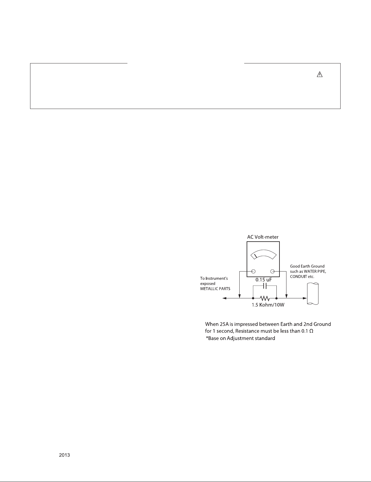
Leakage Current Hot Check (See below Figure)
Plug the AC cord directly into the AC outlet.
Do not use a line Isolation Transformer during this check.
Connect 1.5 K / 10 watt resistor in parallel with a 0.15 uF capacitor
between a known good earth ground (Water Pipe, Conduit, etc.)
and the exposed metallic parts.
Measure the AC voltage across the resistor using AC voltmeter
with 1000 ohms/volt or more sensitivity.
Reverse plug the AC cord into the AC outlet and repeat AC voltage
measurements for each exp ose d metallic par t. Any voltage
measured must not exceed 0.75 volt RMS which is corresponds to
0.5 mA.
In case any measurement is out of the limits specified, there is
possibility of shock hazard and the set must be checked and
repaired before it is returned to the customer.
Leakage Current Hot Check circuit
Only for training and service purposes
- 3 -
LGE Internal Use OnlyCopyright © LG Electronics. Inc. All rights reserved.
Page 4

SERVICING PRECAUTIONS
CAUTION: Before servicing receivers covered by this service
manual and its supplements and addenda, read and follow the
SAFETY PRECAUTIONS on page 3 of this publication.
NOTE: If unforeseen circumstances create conict between the
following servicing precautions and any of the safety precautions
on page 3 of this publication, always follow the safety precautions.
Remember: Safety First.
General Servicing Precautions
1. Always unplug the receiver AC power cord from the AC power
source before;
a. Removing or reinstalling any component, circuit board mod-
ule or any other receiver assembly.
b. Disconnecting or reconnecting any receiver electrical plug or
other electrical connection.
c. Connecting a test substitute in parallel with an electrolytic
capacitor in the receiver.
CAUTION: A wrong part substitution or incorrect polarity
installation of electrolytic capacitors may result in an explosion hazard.
2. Test high voltage only by measuring it with an appropriate
high voltage meter or other voltage measuring device (DVM,
FETVOM, etc) equipped with a suitable high voltage probe.
Do not test high voltage by "drawing an arc".
3. Do not spray chemicals on or near this receiver or any of its
assemblies.
4. Unless specied otherwise in this service manual, clean
electrical contacts only by applying the following mixture to the
contacts with a pipe cleaner, cotton-tipped stick or comparable
non-abrasive applicator; 10 % (by volume) Acetone and 90 %
(by volume) isopropyl alcohol (90 % - 99 % strength)
CAUTION: This is a ammable mixture.
Unless specied otherwise in this service manual, lubrication of
contacts in not required.
5. Do not defeat any plug/socket B+ voltage interlocks with which
receivers covered by this service manual might be equipped.
6. Do not apply AC power to this instrument and/or any of its
electrical assemblies unless all solid-state device heat sinks are
correctly installed.
7. Always connect the test receiver ground lead to the receiver
chassis ground before connecting the test receiver positive
lead.
Always remove the test receiver ground lead last.
8. Use with this receiver only the test xtures specied in this
service manual.
CAUTION: Do not connect the test xture ground strap to any
heat sink in this receiver.
Electrostatically Sensitive (ES) Devices
Some semiconductor (solid-state) devices can be damaged easily by static electricity. Such components commonly are called
Electrostatically Sensitive (ES) Devices. Examples of typical ES
devices are integrated circuits and some eld-effect transistors
and semiconductor “chip” components. The following techniques
should be used to help reduce the incidence of component damage caused by static by static electricity.
1. Immediately before handling any semiconductor component or
semiconductor-equipped assembly, drain off any electrostatic
charge on your body by touching a known earth ground. Alternatively, obtain and wear a commercially available discharging
wrist strap device, which should be removed to prevent potential shock reasons prior to applying power to the unit under test.
2. After removing an electrical assembly equipped with ES
devices, place the assembly on a conductive surface such as
aluminum foil, to prevent electrostatic charge buildup or exposure of the assembly.
3. Use only a grounded-tip soldering iron to solder or unsolder ES
devices.
4. Use only an anti-static type solder removal device. Some solder
removal devices not classied as “anti-static” can generate
electrical charges sufcient to damage ES devices.
5. Do not use freon-propelled chemicals. These can generate
electrical charges sufcient to damage ES devices.
6. Do not remove a replacement ES device from its protective
package until immediately before you are ready to install it.
(Most replacement ES devices are packaged with leads electrically shorted together by conductive foam, aluminum foil or
comparable conductive material).
7. Immediately before removing the protective material from the
leads of a replacement ES device, touch the protective material
to the chassis or circuit assembly into which the device will be
installed.
CAUTION: Be sure no power is applied to the chassis or circuit,
and observe all other safety precautions.
8. Minimize bodily motions when handling unpackaged replacement ES devices. (Otherwise harmless motion such as the
brushing together of your clothes fabric or the lifting of your
foot from a carpeted oor can generate static electricity sufcient to damage an ES device.)
General Soldering Guidelines
1. Use a grounded-tip, low-wattage soldering iron and appropriate
tip size and shape that will maintain tip temperature within the
range or 500 °F to 600 °F.
2. Use an appropriate gauge of RMA resin-core solder composed
of 60 parts tin/40 parts lead.
3. Keep the soldering iron tip clean and well tinned.
4. Thoroughly clean the surfaces to be soldered. Use a mall wirebristle (0.5 inch, or 1.25 cm) brush with a metal handle.
Do not use freon-propelled spray-on cleaners.
5. Use the following unsoldering technique
a. Allow the soldering iron tip to reach normal temperature.
(500 °F to 600 °F)
b. Heat the component lead until the solder melts.
c. Quickly draw the melted solder with an anti-static, suction-
type solder removal device or with solder braid.
CAUTION: Work quickly to avoid overheating the circuit
board printed foil.
6. Use the following soldering technique.
a. Allow the soldering iron tip to reach a normal temperature
(500 °F to 600 °F)
b. First, hold the soldering iron tip and solder the strand against
the component lead until the solder melts.
c. Quickly move the soldering iron tip to the junction of the
component lead and the printed circuit foil, and hold it there
only until the solder ows onto and around both the component lead and the foil.
CAUTION: Work quickly to avoid overheating the circuit
board printed foil.
d. Closely inspect the solder area and remove any excess or
splashed solder with a small wire-bristle brush.
Only for training and service purposes
- 4 -
LGE Internal Use OnlyCopyright © LG Electronics. Inc. All rights reserved.
Page 5

IC Remove/Replacement
Some chassis circuit boards have slotted holes (oblong) through
which the IC leads are inserted and then bent at against the circuit foil. When holes are the slotted type, the following technique
should be used to remove and replace the IC. When working with
boards using the familiar round hole, use the standard technique
as outlined in paragraphs 5 and 6 above.
Removal
1. Desolder and straighten each IC lead in one operation by
gently prying up on the lead with the soldering iron tip as the
solder melts.
2. Draw away the melted solder with an anti-static suction-type
solder removal device (or with solder braid) before removing
the IC.
Replacement
1. Carefully insert the replacement IC in the circuit board.
2. Carefully bend each IC lead against the circuit foil pad and
solder it.
3. Clean the soldered areas with a small wire-bristle brush.
(It is not necessary to reapply acrylic coating to the areas).
"Small-Signal" Discrete Transistor
Removal/Replacement
1. Remove the defective transistor by clipping its leads as close
as possible to the component body.
2. Bend into a "U" shape the end of each of three leads remaining
on the circuit board.
3. Bend into a "U" shape the replacement transistor leads.
4. Connect the replacement transistor leads to the corresponding
leads extending from the circuit board and crimp the "U" with
long nose pliers to insure metal to metal contact then solder
each connection.
Power Output, Transistor Device
Removal/Replacement
1. Heat and remove all solder from around the transistor leads.
2. Remove the heat sink mounting screw (if so equipped).
3. Carefully remove the transistor from the heat sink of the circuit
board.
4. Insert new transistor in the circuit board.
5. Solder each transistor lead, and clip off excess lead.
6. Replace heat sink.
Diode Removal/Replacement
1. Remove defective diode by clipping its leads as close as possible to diode body.
2. Bend the two remaining leads perpendicular y to the circuit
board.
3. Observing diode polarity, wrap each lead of the new diode
around the corresponding lead on the circuit board.
4. Securely crimp each connection and solder it.
5. Inspect (on the circuit board copper side) the solder joints of
the two "original" leads. If they are not shiny, reheat them and if
necessary, apply additional solder.
3. Solder the connections.
CAUTION: Maintain original spacing between the replaced
component and adjacent components and the circuit board to
prevent excessive component temperatures.
Circuit Board Foil Repair
Excessive heat applied to the copper foil of any printed circuit
board will weaken the adhesive that bonds the foil to the circuit
board causing the foil to separate from or "lift-off" the board. The
following guidelines and procedures should be followed whenever
this condition is encountered.
At IC Connections
To repair a defective copper pattern at IC connections use the
following procedure to install a jumper wire on the copper pattern
side of the circuit board. (Use this technique only on IC connections).
1. Carefully remove the damaged copper pattern with a sharp
knife. (Remove only as much copper as absolutely necessary).
2. carefully scratch away the solder resist and acrylic coating (if
used) from the end of the remaining copper pattern.
3. Bend a small "U" in one end of a small gauge jumper wire and
carefully crimp it around the IC pin. Solder the IC connection.
4. Route the jumper wire along the path of the out-away copper
pattern and let it overlap the previously scraped end of the
good copper pattern. Solder the overlapped area and clip off
any excess jumper wire.
At Other Connections
Use the following technique to repair the defective copper pattern
at connections other than IC Pins. This technique involves the
installation of a jumper wire on the component side of the circuit
board.
1. Remove the defective copper pattern with a sharp knife.
Remove at least 1/4 inch of copper, to ensure that a hazardous
condition will not exist if the jumper wire opens.
2. Trace along the copper pattern from both sides of the pattern
break and locate the nearest component that is directly connected to the affected copper pattern.
3. Connect insulated 20-gauge jumper wire from the lead of the
nearest component on one side of the pattern break to the lead
of the nearest component on the other side.
Carefully crimp and solder the connections.
CAUTION: Be sure the insulated jumper wire is dressed so the
it does not touch components or sharp edges.
Fuse and Conventional Resistor
Removal/Replacement
1. Clip each fuse or resistor lead at top of the circuit board hollow
stake.
2. Securely crimp the leads of replacement component around
notch at stake top.
Only for training and service purposes
- 5 -
LGE Internal Use OnlyCopyright © LG Electronics. Inc. All rights reserved.
Page 6

SPECIFICATION
NOTE : Specifications and others are subject to change without notice for improvement
1. Application range
This spec sheet is applied all of the 32”, 39", 42”,47”,55”,60”, 65” LED TV with LT33B chassis
2. Test condition
Each part is tested as below without special notice.
1) Temperature : 25 ºC ± 5 ºC, CST : 40 ºC±5 ºC
2) Relative Humidity: 65 % ± 10 %
3) Power Voltage
Standard input voltage (100~240V@ 50/60Hz)
* Standard Voltage of each products is marked by models.
4) Specification and performance of each parts are followed each drawing and specification by part number in accordance with
BOM.
5) The receiver must be operated for about 20 minutes prior to the adjustment.
3. Test method
1) Performance: LGE TV test method followed
2) Demanded other specification
- Safety : CE, IEC specification
- EMC: CE, IEC
.
Only for training and service purposes
- 6 -
LGE Internal Use OnlyCopyright © LG Electronics. Inc. All rights reserved.
Page 7
4. General Specification
No Item Specication Remark
1. Display Screen Device 32” wide Color Display Module Resolution: 1366*768 (32LN570)
32” wide Color Display Module Resolution: 1920*1080
39” wide Color Display Module Resolution: 1920*1080
42” wide Color Display Module Resolution: 1920*1080
47” wide Color Display Module Resolution: 1920*1080
50” wide Color Display Module Resolution: 1920*1080
55” wide Color Display Module Resolution: 1920*1080
60” wide Color Display Module Resolution: 1920*1080
2. Aspect Ratio 16:9 All
3. LCD Module 32" TFT WUXGA LCD
32" TFT WXGA LCD Only 32LN570B
42" TFT WUXGA LCD
47” TFT WUXGA LCD
50” TFT WUXGA LCD
55” TFT WUXGA LCD
60” TFT WUXGA LCD
4. Operating Environment TFT 1) Temp. : 0 ~ 40 deg
5. Storage Environment TFT 1) Temp. : -20 ~ 60 deg
6. Input Voltage AC100 ~ 240V, 50/60Hz
7. Power Consumption(Max) =
LCD(Module) + Backlight(LED)
FHD
T240Hz
POLA
FHD
T120Hz POLA
FHD 60Hz POLA
FHD
T120Hz
CINEMA
FHD
T120Hz
Edge
FHD
T120Hz
Direct
HD (32” only)
FHD 60Hz
Direct
(32/39/42/47”)
POLA (55”)
2) Humidity : 0 ~ 85%
2) Humidity : 10 ~ 90%
60 TBD W
TBD W
120 W
55 TBD W FPR : LC550EUJ-SEK1 [55LA6200-DA]
55 TBD W Normal : LC550EUJ-SEE1 [55LN5700-DC]
42” 56.4 W
47” 62.4 W FPR: LC470EUG-KFF1 [47LA66/68 6900-DA]
55” 74.3 W FPR: LC550EUG-KFF1 [55LA66/68/6900-DA]
42” 57 W FPR: LC420EUN-SFF2 [42LA6400-DA]
47” 68 W FPR: LC470EUN-SFF2 [47LA6400-DA]
50” 76 W FPR: LC500EUN-SFF1 [50LA6400-DA]
50” 70.5 W FPR: T500HVD02.1[50LA6600-DA]
55” 88 W FPR: LC550EUN-SFF1 [55LA6400-DA]
42” 77 W FPR : LC420DUE-SFU1 [42LA6200-DA]
77 W Normal : LC420DUE-SFR1 [42LN5700-DH]
47” 91 W FPR : LC470DUE-SFU1 [47LA6200-DA]
91 W Normal : LC470DUE-SFR1 [47LN5700-DH]
50” 108 W FPR : LC500DUE-SFU1 [50LA6200-DA]
42” 62.34 W Normal : LC420DUE-SFR1 [42LN5700]
47” 91 W Normal : LC470DUE-SFR1 [47LN5700-DH]
55” Normal : LC550DUK-SEE1 [55LN5700-DC]
39” W HC390DUN- VCFP1[39LN5700/5730]
32” 39.2 W LC320DXE-SFR1 [32LN570B (HD)]
38 W LC320DUE-SFR1 [32LN5700(FHD)]
LGE SPEC
FPR : LC600DUK-SEF1 [60LA6200-DA]
FPR: HC600DUD-SLFO1[60LA7400-DA].
Normal : HC600DUD-SLFP1
FPR: LC420EUG-KFF1 [42LA65/66/68/6900-DA]
Only for training and service purposes
- 7 -
LGE Internal Use OnlyCopyright © LG Electronics. Inc. All rights reserved.
Page 8
8. LCD Module Size Maker Inch (H) × (V) × (D)
LGD 32” TBD LC320EUA-KFF1 [32LA6900-DA]
947.7 x 546.65 x 9.7 LC420EUG-KFF1 [42LA66/68/6900-DA]
42” 958 x 559.1 x 9.9 LC420EUN-SFF2 [42LA6400-DA]
956.4 x 555.0 x 37.4 LC420DUE-SFU1 [42LA6200-DA]
958.2 x 555.8 x 35.0 LC420DUE-SFR1 [42LN5700-DH]
47” 1059.5 x 609.5 x 9.7 LC470EUG-KFF1 [47LA66/68/6900-DA]
1070.6 x 622.0 x 9.9 LC470EUN-SFF2 [47LA6400-DA]
1068.0 x 617.8 x 38.8 LC470DUE-SFU1 [47LA6200-DA]
1067.6 x 617.4 x 36.5 LC470DUE-SFR1 [47LN5700-DH]
50” 1121.6 x 644.3 x 10.8 LC500EUN-SFF1 [50LA6400-DA]
1123.0 x 648.2 x 40.3 LC500DUE-SFU1 [50LA6200-DA]
55” 1229.4 x 706.3 x 13.2 LC550EUG-KFF1 [55LA66/68/6900-DA]
1244.6 x 720.9 x 9.9 LC550EUN-SFF1 [55LA6400-DA]
1232.0 x 704.0 x 1.94 LC550EUJ-SEK1 [55LA6200-DA]
1232.0 x 704.0 x 1.94 LC550EUJ-SEE1 [55LN5700-DC]
60” 1333.0 x 758.94 x 1.42 LC600DUK-SEF1 [60LA6200-DA]
1346.8 x 774.4 x 29.9 HC600DUD-SLFP1[60LN5700-DA]
CMI 39” 853.92 × 480.33 ×38.5 HC390DUN- VCFP1[39LN5700/5730]
AUO 50” 1111.8x637.3x26.2 T500HVD02.1[50LA6600-DA]
HeeSung 60” 1346.8 x 774.4 x 29.9 HC600DUD-SLFO1[60LA7400-DA].
Pixel Pitch Maker Inch (H) × (V) × (D)
LGD 32” TBD LC320EUA-KFF1 [32LA6900-DA]
170.25 x 510.75 LC320DUE-SFR1 [32LN570B]
42” 483.3 x 483.3 LC420EUG-KFF1 [42LA66/68/6900-DA]
483.3 x 483.3 LC420EUN-SFF2 [42LA6400-DA]
483.3 x 483.3 LC420DUE-SFU1 [42LA6200-DA]
483.3 x 483.3 LC420DUE-SFR1 [42LN56/5700-DA]
47” 541.5 x 541.5 LC470EUG-KFF1 [47LA66/68/6900-DA]
541.5 x 541.5 LC470EUN-SFF2 [47LA6400-DA]
541.5 x 541.5 LC470DUE-SFU1 [47LA6200-DA]
541.5 x 541.5 LC470DUE-SFR1 [47LN5700-DH]
50” 570.75 x 570.75 LC500EUN-SFF1 [50LA6400-DA]
570.75 x 570.75 LC500DUE-SFU1 [50LA6200-DA]
55” 630 x 630 LC550EUG-KFF1 [55LA66/68/6900-DA]
630 x 630 LC550EUN-SFF1 [55LA6400-DA]
630 x 630 LC550EUJ-SEK1 [55LA6200-DA]
630 x 630 LC550EUJ-SEE1 [55LM5700-DC]
60” 687 x 687 LC600DUK-SEF1 [60LA6200-DA]
687 x 687 HC600DUD-SLFP1[60LN5700-DA]
CMI 39” 176.75*530.25 HC390DUN- VCFP1[39LN5700/5730]
AUO 50” 570.75 x 570.75 T500HVD02.1[50LA6600-DA]
HeeSung 60” 687 x 687 HC600DUD-SLFO1[60LA7400-DA].
Only for training and service purposes
- 8 -
LGE Internal Use OnlyCopyright © LG Electronics. Inc. All rights reserved.
Page 9
8. Back Light Maker Inch TYPE Module Name
LGD 32” CINEMA FPR : LC320EUA-KFF1 [32LA6900-DA]
42”
47”
55”
42” Edge FPR: LC420EUN-SFF2 [42LA6400-DA]
47” FPR: LC470EUN-SFF2 [47LA6400-DA]
50” FPR: LC500EUN-SFF1 [50LA6400-DA]
55” FPR: LC550EUN-SFF1 [55LA6400-DA]
55” POLA FPR: LC550EUJ-SEK1 [55LA6200-DA]
60” FPR: LC600DUK-SEF1 [60LA6200-DA]
39” POLA, CMI HC390DUN- VCFP1[39LN5700/5730]
32 Direct LC320DXE-SFR1 [32LN570B-DH]
42 FPR : LC420DUE-SFU1 [42LA6200-DA]
47 FPR : LC470DUE-SFU1 [47LA6200-DA]
50 FPR : LC500DUE-SFU1 [50LA6200-DA]
AUO 50” Edge T500HVD02.1[50LA6600-DA]
HeeSung 60” POLA HC600DUD-SLFO1[60LA7400-DA].
Display Colors 1.06 B (10-bit) Except FHD 60Hz models
16.7 M (8-bit) FHD/HD 60Hz models
Coating 3H(Hard coating), Anti-glare
FPR: LC420EUG-KFF1 [42LA66/68/6900-DA]
FPR: LC470EUG-KFF1 [47LA66/68/6900-DA]
FPR: LC550EUG-KFF1 [55LA66/68/6900-DA]
Normal : LC550EUJ-SEE1 [55LN5700-DC]
Normal : HC600DUD-SLFP1[60LN5700-DA]
Normal : LC420DUE-SFR1 [42LN 5700-DH]
Normal : LC470DUE-SFR1 [47LN5700-DH]
Only for training and service purposes
- 9 -
LGE Internal Use OnlyCopyright © LG Electronics. Inc. All rights reserved.
Page 10
5. External Input Support Format
5.1. Component input(Y, CB/PB, CR/PR)
No Resolution H-freq(kHz) V-freq.(kHz) Pixel clock Proposed
1. 720*480 15.73 60 13.5135 SDTV ,DVD 480I
2. 720*480 15.73 59.94 13.5 SDTV ,DVD 480I
3. 720*480 31.50 60 27.027 SDTV 480P
4. 720*480 31.47 59.94 27.00 SDTV 480P
5. 720*576 15.625 50* 13.5 SDTV 576I
6. 720*576 31.25 50* 13.5 SDTV 576P
7. 1280*720 37.5 50* 74.25 HDTV 720P
8. 1280*720 45.00 60.00 74.25 HDTV 720P
9. 1280*720 44.96 59.94 74.176 HDTV 720P
10. 1929*1080 28.125 50* 74.25 HDTV 1080I
11. 1920*1080 33.75 60.00 74.25 HDTV 1080I
12. 1920*1080 33.72 59.94 74.176 HDTV 1080I
13. 1920*1080 56.25 50* 148.5 HDTV 1080P
14. 1920*1080 67.50 60 148.50 HDTV 1080P
15. 1920*1080 67.432 59.94 148.352 HDTV 1080P
16. 1920*1080 27.00 24.00 74.25 HDTV 1080P
17. 1920*1080 26.97 23.976 74.176 HDTV 1080P
18. 1920*1080 33.75 30.00 74.25 HDTV 1080P
19. 1920*1080 33.71 29.97 74.176 HDTV 1080P
Only for training and service purposes
- 10 -
LGE Internal Use OnlyCopyright © LG Electronics. Inc. All rights reserved.
Page 11
5.2. HDMI : EDID DATA : Refer to adjust specification
5.2.1. DTV mode
No Resolution H-freq(kHz) V-freq.(Hz)
1 720*480 15.73 59.94 13.500 SDTV, DVD 480I(525I) Spec. out but display
2 15.75 60.00 13.514 SDTV, DVD 480I(525I)
3 720*576 15.625 50.00 13.500 SDTV, DVD 576I(625I) 50Hz
4 720*480 31.47 59.94 27 SDTV 480P
5 31.5 60.00 27.027 SDTV 480P
6 720*576 31.25 50.00 27 SDTV 576P
7 1280*720 44.96 59.94 74.176 HDTV 720P
8 45 60.00 74.25 HDTV 720P
9 37.5 50.00 74.25 HDTV 720P
10 1920*1080 28.125 50.00 74.25 HDTV 1080I
11 33.72 59.94 74.176 HDTV 1080I
12 33.75 60.00 74.25 HDTV 1080I
13 26.97 23.976 63.296 HDTV 1080P
14 27.00 24.000 63.36 HDTV 1080P
15 33.71 29.97 79.120 HDTV 1080P
16 33.75 30.00 79.20 HDTV 1080P
17 56.25 50.00 148.5 HDTV 1080P
18 67.432 59.94 148.350 HDTV 1080P
19 67.5 60.00 148.5 HDTV 1080P
Pixel
clock(MHz)
Proposed Remark
5.2.2. PC mode
No. Resolution H-freq(kHz) V-freq.(kHz) Pixel clock Proposed Remarks
1 640*350 31.468 70.09 25.17 EGA
2 720*400 31.469 70.09 28.32 DOS
3 640*480 31.469 59.94 25.17 VESA(VGA)
4 800*600 37.879 60.31 40 VESA(SVGA)
5 1024*768 48.363 60.00 65 VESA(XGA)
6 1152*864 54.348 60.053 80.002 VESA(VGA)
7 1360*768 47.712 60.015 84.75 VESA(WXGA)
8 1280*1024 63.981 60.020 109.00 SXGA
9 1920*1080 67.5 60 158.40 WUXGA (Reduced Blanking) Only FHD Model
Only FHD Model (Support to HDMI-PC)
Only for training and service purposes
- 11 -
LGE Internal Use OnlyCopyright © LG Electronics. Inc. All rights reserved.
Page 12

5.3. 3D mode
5.3.1. RF Input
No Resolution Proposed 3D input proposed mode
1 HD 1080I
720P
2 SD 576P
576I
5.3.2. RF Input (3D supported mode automatically)
No Signal 3D input proposed mode
1 Frame Compatible Side by Side(Half), Top & Bottom
5.3.3. HDMI Input 1.3(3D supported mode manually)
No Resolution H-freq(kHz) V-freq.(Hz) Pixel clock(MHz) Proposed Remark
1 1280*720 45.00 60.00 74.25 HDTV 720P 2D to 3D
2 1280*720 37.500 50 74.25 HDTV 720P 2D to 3D
3 1920*1080 33.75 60.00 74.25 HDTV 1080I 2D to 3D
4 1920*1080 28.125 50.00 74.25 HDTV 1080I 2D to 3D
5 1920*1080 27.00 24.00 74.25 HDTV 1080P 2D to 3D
6 1920*1080 28.12 25 74.25 HDTV 1080P 2D to 3D
7 1920*1080 33.75 30.00 74.25 HDTV 1080P 2D to 3D
8 1920*1080 56.25 50 148.5 HDTV 1080P 2D to 3D
9 1920*1080 67.50 60.00 148.5 HDTV 1080P 2D to 3D
2D to 3D
Side by Side(Half)
Top & Bottom
2D to 3D
Side by Side(half),
Top & Bottom,
Single Frame Sequential
Side by Side(half),
Top & Bottom,
Single Frame Sequential
Side by Side(half),
Top & Bottom
Side by Side(half),
Top & Bottom
Side by Side(half),
Top & Bottom,
Checkerboard
Side by Side(half),
Top & Bottom,
Checkerboard
Side by Side(half),
Top & Bottom,
Checkerboard
Side by Side(half),
Top & Bottom,
Checkerboard,
Single Frame Sequential,
Row Interleaving,
Column Interleaving
Side by Side(half),
Top & Bottom,
Checkerboard,
Single Frame Sequential,
Row Interleaving,
Column Interleaving
Only for training and service purposes
- 12 -
LGE Internal Use OnlyCopyright © LG Electronics. Inc. All rights reserved.
Page 13
5.3.4. HDMI Input 1.4b (3D supported mode automatically)
No Resolution H-freq(kHz) V-freq.(Hz) Pixel clock(MHz) 3D input proposed
mode
1 640*480 31.469 / 31.5 59.94/ 60 25.175/25.2 Top-and-Bottom
Side-by-side(half)
2 62.938 / 63 59.94/ 60 50.35/50.4 Frame packing
Line alternative
3 31.469 / 31.5 59.94/ 60 50.35/50.4 Side-by-side(Full) (SDTV 480P)
4 720*480 31.25 50 27 Top-and-Bottom
Side-by-side(half)
5 62.5 50 54 Frame packing
Line alternative
6 31.25 50 54 Side-by-side(Full) (SDTV 480P)
7 720*576
(576p)
8 62.5 50 54 Frame packing
9 31.25 50 54 Side-by-side(Full) (SDTV 576P)
720 (1440)*576
10 15.625 50 27 Top-and-Bottom
(576i)
11 31.25 50 54 Frame packing
12 15.625 50 54 Side-by-side(Full) (SDTV 576I)
13 1280*720 37.5 50 74.25 Top-and-Bottom
14 75 50 148.5 Frame packing
15 37.5 50 148.5 Side-by-side(Full) (HDTV 720P)
16 44.96 / 45 59.94 / 60 74.18/74.25 Top-and-Bottom
17 89.91 / 90 59.94 / 60 148.35/148.5 Frame packing
18 44.96 / 45 59.94 / 60 148.35/148.5 Side-by-side(Full) (HDTV 720P)
31.25 50 27 Top-and-Bottom
Side-by-side(half)
Line alternative
Side-by-side(half)
Field alternative
Side-by-side(half)
Line alternative
Side-by-side(half)
Line alternative
Secondary(SDTV 480P)
Secondary(SDTV 480P)
Secondary(SDTV 480P)
(SDTV 480P)
Secondary(SDTV 480P)
Secondary(SDTV 480P)
Secondary(SDTV 480P)
(SDTV 480P)
Secondary(SDTV 576P)
Secondary(SDTV 576P)
Secondary(SDTV 576P)
(SDTV 576P)
Secondary(SDTV 576I)
Secondary(SDTV 576I)
Secondary(SDTV 576I)
(SDTV 576I)
Primary(HDTV 720P)
Primary(HDTV 720P)
Primary(HDTV 720P)
(HDTV 720P)
Primary(HDTV 720P)
Primary(HDTV 720P)
Primary(HDTV 720P)
(HDTV 720P)
Proposed
Only for training and service purposes
- 13 -
LGE Internal Use OnlyCopyright © LG Electronics. Inc. All rights reserved.
Page 14
No Resolution H-freq(kHz) V-freq.(Hz) Pixel clock(MHz) 3D input proposed
mode
19 1920*1080 33.72 / 33.75 59.94 / 60 74.18/74.25 Top-and-Bottom
Side-by-side(half)
20 67.432 / 67.5 59.94 / 60 148.35/148.5 Frame packing
Field alternative
21 33.72 / 33.75 59.94 / 60 148.35/148.5 Side-by-side(Full) (HDTV 1080I)
22 28.125 50.00 74.25 Top-and-Bottom
Side-by-side(half)
23 56.25 50.00 148.5 Frame packing
Field alternative
24 28.125 50.00 148.5 Side-by-side(Full) (HDTV 1080I)
25 26.97 / 27 23.97 / 24 74.18/74.25 Top-and-Bottom
Side-by-side(half)
26 43.94 / 54 23.97 / 24 148.35/148.5 Frame packing
Line alternative
27 26.97 / 27 23.97 / 24 148.35/148.5 Side-by-side(Full) (HDTV 1080P)
28 28.12 25 74.25 Top-and-Bottom
Side-by-side(half)
29 56.25 25 148.5 Frame packing
Line alternative
30 28.125 25 148.5 Side-by-side(Full) (HDTV 1080P)
31 33.716 / 33.75 29.976 / 30.00 74.18/74.25 Top-and-Bottom
Side-by-side(half)
32 67.432 / 67.5 29.976 / 30.00 148.35/148.5 Frame packing
Line alternative
33 33.716 / 33.75 29.976 / 30.00 148.35/148.5 Side-by-side(Full) (HDTV 1080P)
34 56.25 50 148.5 Top-and-Bottom
Side-by-side(half)
35 67.43 / 67.5 59.94 / 60 148.35/148.50 Top-and-Bottom
Side-by-side(half)
Secondary(HDTV 1080I)
Primary(HDTV 1080I)
Primary(HDTV 1080I)
(HDTV 1080I)
Secondary(HDTV 1080I)
Primary(HDTV 1080I)
Primary(HDTV 1080I)
(HDTV 1080I)
Primary(HDTV 1080P)
Primary(HDTV 1080P)
Primary(HDTV 1080P)
(HDTV 1080P)
Secondary(HDTV 1080P)
Secondary(HDTV 1080P)
Secondary(HDTV 1080P)
(HDTV 1080P)
Primary(HDTV 1080P)
Secondary(HDTV 1080P)
Primary(HDTV 1080P)
(HDTV 1080P)
Primary(HDTV 1080P)
Secondary(HDTV 1080P)
Primary(HDTV 1080P)
Secondary(HDTV 1080P)
Proposed
5.3.5. HDMI-PC 3D Input (3D supported mode manually)
No Resolution H-freq(kHz) V-freq.(Hz) Pixel clock(MHz) 3D input proposed mode Proposed
1 1024*768 48.36 60 65 2D to 3D,
Side by Side(half)
Top & Bottom
2 1360*768 47.71 60 85.5 2D to 3D,
Side by Side(half)
Top & Bottom
3 1920*1080 67.500 60 148.50 2D to 3D,
Side by Side(half)
Top & Bottom,
Checker Board,
Single Frame Sequential
Row Interleaving,
Column Interleaving
4 Others - - - 2D to 3D 640*350
- 14 -
Only for training and service purposes
HDTV 768P
HDTV 768P
HDTV 1080P
720*400
640*480
800*600
1152*864
LGE Internal Use OnlyCopyright © LG Electronics. Inc. All rights reserved.
Page 15
5.3.6. Component 3D Input (3D supported mode manually)
No Resolution H-freq(kHz) V-freq.(Hz) Pixel clock(MHz) 3D input proposed mode Proposed
1 1280*720 37.5 50 74.25 2D to 3D,
Side by Side(half),
Top & Bottom
2 1280*720 45.00 60.00 74.25 2D to 3D,
Side by Side(half),
Top & Bottom
3 1280*720 44.96 59.94 74.176 2D to 3D,
Side by Side(half)
Top & Bottom
4 1920*1080 33.75 60.00 74.25 2D to 3D,
Side by Side(half)
Top & Bottom
5 1920*1080 33.72 59.94 74.176 2D to 3D,
Side by Side(half)
Top & Bottom
6 1920*1080 28.12 50 74.25 2D to 3D,
Side by Side(half)
Top & Bottom
7 1920*1080 67.500 60 148.50 2D to 3D,
Side by Side(half)
Top & Bottom
8 1920*1080 67.432 59.94 148.352 2D to 3D,
Side by Side(half)
Top & Bottom
9 1920*1080 27.000 24.000 74.25 2D to 3D,
Side by Side(half)
Top & Bottom
10 1920*1080 28.12 25 74.25 2D to 3D,
Side by Side(half)
Top & Bottom
11 1920*1080 56.25 50 74.25 2D to 3D,
Side by Side(half)
Top & Bottom
12 1920*1080 26.97 23.976 74.176 2D to 3D,
Side by Side(half)
Top & Bottom
13 1920*1080 33.75 30.000 74.25 2D to 3D,
Side by Side(half)
Top & Bottom
14 1920*1080 33.71 29.97 74.176 2D to 3D,
Side by Side(half)
Top & Bottom
HDTV 720P
HDTV 720P
HDTV 720P
HDTV 1080I
HDTV 1080I
HDTV 1080I
HDTV 1080P
HDTV 1080P
HDTV 1080P
HDTV 1080P
HDTV 1080P
HDTV 1080P
HDTV 1080P
HDTV 1080P
Only for training and service purposes
- 15 -
LGE Internal Use OnlyCopyright © LG Electronics. Inc. All rights reserved.
Page 16
5.3.7. USB Input (3D) (3D supported mode manually)
No Resolution H-freq(kHz) V-freq.(Hz) Pixel clock(MHz) 3D input proposed mode Proposed
1 1920*1080 33.75 30 74.25 2D to 3D
Side by Side(Half)*,
Top & Bottom*,
Checkerboard*
Row Interleaving,
Column Interleaving
(Photo : side by Side(half),
Top & Bottom)
HDTV 1080P
5.2.8. DLNA Input (3D)
No Resolution H-freq(kHz) V-freq.(Hz) Pixel clock(MHz) 3D input proposed mode Proposed
1 1920*1080 33.75 30 74.25 2D to 3D
Side by Side(Half)*,
Top & Bottom*,
Checkerboard*
Row Interleaving,
Column Interleaving
(Photo : side by Side(half), Top
& Bottom)
HDTV 1080P
Only for training and service purposes
- 16 -
LGE Internal Use OnlyCopyright © LG Electronics. Inc. All rights reserved.
Page 17

ADJUSTMENT INSTRUCTION
1. Application Range
This specification sheet is applied all of the LT33B LED TV
models, which produced in manufacture department or similar
LG TV factory
2. Specification
(1) Because this is not a hot chassis, it is not necessary to use
an isolation transformer. However, the use of isolation
transformer will help protect test instrument.
(2) Adjustment must be done in the correct order. But it is
flexible when its factory local problem occurs.
(3) The adjustment must be performed in the circumstance of
25 ±5ºC of temperature and 65±10% of relative humidity if
there is no specific designation.
(4) The input voltage of the receiver must keep 100~220V,
50/60Hz.
(5) Before adjustment, execute Heat-Run for 5 minutes.
▪ After Receive 100% Full white pattern (06CH) then process
Heat-run
(or “8. Test pattern” condition of Ez-Adjust status)
▪ How to make set white pattern
1) Press Power ON button of Service Remocon
2) Pr ess ADJ button of Service remocon. Select “8. Test
pattern” and, after select “White” using navigation button,
and then you can see 100% Full White pattern.
* In this status you can maintain Heat-Run useless any pattern
generator
* Notice : if you mai nt ain one pictu re ov er 20 minutes
(Especially sharp distinction black with white pattern
-13Ch, or Cross hatch pattern – 09Ch) then it can
appear image stick near black level.
4. PCB Assembly Adjustment
4.1. MAC Address, ESN Key and Widevine
Key download
4.1.1. Equipment & Condition
1) Play file: keydownload.exe
4.1.2. Communication Port connection
1) Key Write: Com 1,2,3,4 and 115200 (Baudrate)
2) Barcode: Com 1,2,3,4 and 9600 (Baudrate)
4.1.3. Download process
1) Select the download items.
2) Mode check: Online Only
3) Check the test process
- DETECT -> MAC_WRITE -> ESN_WRITE -> WIDEVINE_
WRITE
4) Play : START
5) Check of result: Ready, Test, OK or NG
4.1.4. Communication Port connection
1) Connect: PCBA Jig -> RS-232C Port == PC -> RS-232C
Port
3. Adjustment items
3.1. PCB Assembly Adjustment
▪ MAC Address / ESN / Widevine Download
▪ EDID (The Extended Display Identification Data)/D DC
(Display Data Channel) download
* If it is necessary, it can adjustment at Manufacture Line
You can see set adjustment status at “1. ADJUST CHECK”
of the “In-start menu”
3.2. Set Assembly Adjustment
▪ Color Temperature (White Balance) Adjustment
▪ Using RS-232C
▪ PING Test
▪ Selection Factory output option
Only for training and service purposes
4.1.5. Download
1) 13Y LCD TV+MAC+Widevine+ESN Key+ HDCP1.4 and
HDCP2.0
4.1.6. Inspection
- In INSTART menu, check these keys.
- 17 -
LGE Internal Use OnlyCopyright © LG Electronics. Inc. All rights reserved.
Page 18

4.2. LAN PORT INSPECTION(PING TEST)
4.2.1. Equipment setting
1) Play the LAN Port Test PROGRAM.
2) Input IP set up for an inspection to Test
Program.
*IP Number : 12.12.2.2.
4.2.2. LAN PORT inspection (PING TEST)
1) Play the LAN Port Test Program.
2) connect each other LAN Port Jack.
3) Play Test (F9) button and confirm OK Message.
4) remove LAN CABLE
4.3. ADC Adjust => No need at Assembly
line because of OPT type
* OTP mode
Automatic ADC Calibration. (Internal ADC Calibration) On the
manufacture line, OTP is used
for ADC Calibration automatically.
* External mode
Manual ADC Calibration. When OTP mode is failed, ADC
calibration should be “OK” by
using External mode.
- If you want re-adjust for ADC.
■ Enter Service Mode by pushing “ADJ” key,
■ Enter Internal ADC mode by pushing “►” key at “6. ADC
Calibration”
■
Adjustment protocol
Order Command Set response
(1) Inter the Adjustment mode aa 00 00 a 00 OK00x
(2) Change the Source xb 00 40
xb 00 60
(3) Start Adjustment ad 00 10
(4) Return the Response OKx ( Success condition )
(5) Read Adjustment data ( main)
ad 00 20
( main )
ad 00 30
(6) Conrm Adjustment ad 00 99 NG 03 00x (Failed condition)
(7) End of Adjustment ad 00 90 d 00 OK90x
b 00 OK40x (Adjust 480i Comp1 )
(Adjust 1080p Comp1)
b 00 OK60x (Adjust 1080p RGB)
NGx ( Failed condition )
(main : component1 480i, RGB 1080p)
000000000000000000000000007c007b006dx
(main : component1 1080p)
000000070000000000000000007c0083
0077x
NG 03 01x (Failed condition)
NG 03 02x (Failed condition)
OK 03 03x (Success condition)
Only for training and service purposes
- 18 -
LGE Internal Use OnlyCopyright © LG Electronics. Inc. All rights reserved.
Page 19

5. Factory Adjustment
5.1. EDID (The Extended Display Identification
Data)/DDC (Display Data Channel) Download
● Summary
▪ It is established in VESA, for communication between PC
and Monitor without order from user for building user
condition. It helps to make easily use realize “Plug and Play”
function. For EDID data write, we use DDC2B protocol.
● Auto Download (No need Writing EDID data in Assembly line)
▪ After Set Tool Option, then TV turn off and on finish auto
download
* EDID data for 3DTV (LA62/64/66/68/69/74 Seriese) (Model
name = LG TV ) .
*Rev. 15xxx to confirm that, Rev. up subject to change
- HDMI EDID table
* EDID data for Non-3DTV (LN56/57 Seriese) (Model name =
LG TV )
*Rev. 15xxx to confirm that, Rev. up subject to change
- HDMI EDID table
- HDMI-1 EDID table (0X43, 0x8A)
(1) HDMI 1 Check sum : 0x43, 0X8A (CEA Block 0x21 :10)
(2) HDMI 2 Check sum : 0x43, 0X7A (CEA Block 0x21 :20)
(3) HDMI 3 Check sum : 0x43, 0X6A (CEA Block 0x21 :30)
- HDMI-1 EDID table (0xE8, 0xCC)
(1) HDMI 1 Check sum : 0xE8, 0XCC (CEA Block 0x21 :10)
(2) HDMI 2 Check sum : 0xE8, 0XBC (CEA Block 0x21 :20)
(3) HDMI 3 Check sum : 0xE8, 0XAC (CEA Block 0x21 :30)
Only for training and service purposes
- 19 -
LGE Internal Use OnlyCopyright © LG Electronics. Inc. All rights reserved.
Page 20

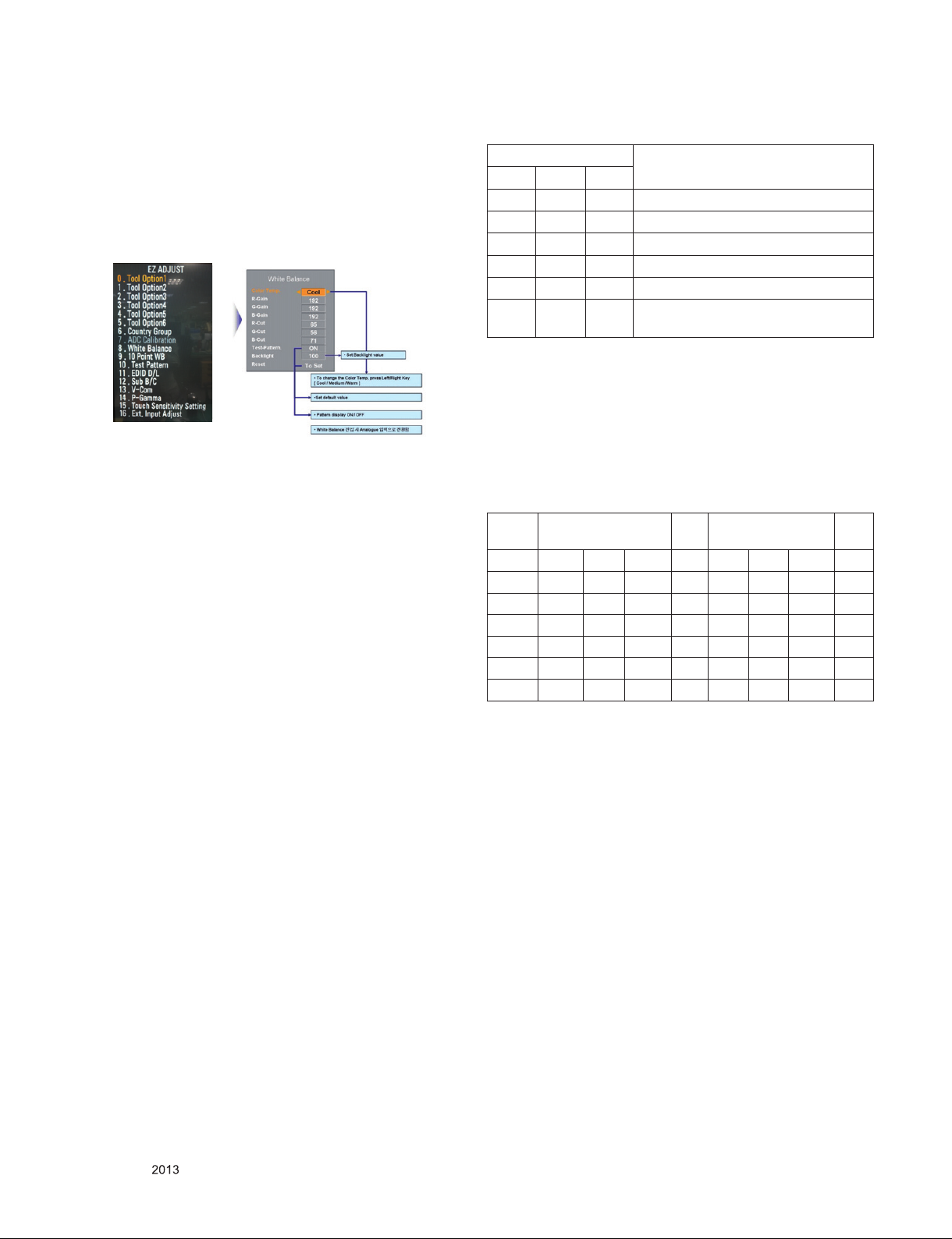
5.2. Adjustment White balance
● W/B Equipment condition
CA210 : CH 9, Test signal : Inner pattern (80IRE) – LAMP
Module
CH14 , Test signal : Inner pattern (80IRE) – LED Module
● Above 5 minutes H/run in the inner pattern. (“power on” key of
adjust remote control)
※ The spec of color temperature and coordinate.
X=0.269
Cool (C50) 13,000k K
All
Medium (0) 9,300k K
Warm (W50) 6,500k K
※ LA6xxx, LA7xxx, LA8xxx, LN5x Series (Normal Line)
Cool Medium Warm
H/R Time(Min)
1 0-2 281 287 295 310 320 342
2 3-5 280 285 294 308 319 340
3 6-9 278 284 292 307 317 339
4 10-19 276 281 290 304 315 336
5 20-35 275 277 289 300 314 332
6 36-49 274 274 288 297 313 329
7 50-79 273 272 287 295 312 327
8 80-119 272 271 286 294 311 326
9 Over 120 271 270 285 293 310 325
x y x x y x
271 270 285 293 313 329
※ LA6xxx, LA7xxx, LA8xxx, LN5x Series (Aging Chamber)
Cool Medium Warm
H/R Time(Min)
1 0-5 280 285 294 308 319 340
2 6-10 276 280 290 303 315 335
3 11-20 272 275 286 298 311 330
4 21-30 269 272 283 295 308 327
5 31-40 267 268 281 291 306 323
6 41-50 266 265 280 288 305 320
7 51-80 265 263 279 286 304 318
8 81-119 264 261 278 284 303 316
9 Over 120 264 260 278 283 303 315
x y x x y x
271 270 285 293 313 329
(±0.002)
Y=0.273
(±0.002)
X=0.285
(±0.002)
Y=0.293
(±0.002)
X=0.313
(±0.002)
Y=0.329
(±0.002)
<Test signal>
- Inner pattern
for W/B adjust
- External white
pattern (80IRE,
204gray)
※ Connecting picture of the measuring instrument (On Automatic
control)
Inside PATTERN is used when W/B is controlled. Connect to
auto controller or push Adjustment R/C POWER-ON -> Enter
the mode of White-Balance, the pattern will come out
● Auto-control interface and directions
(1) Adjust in the place where the influx of light like floodlight
around is blocked. (Illumination is less than 10ux).
(2) Adhere closely the Color Analyzer ( CA210 ) to the module
less than 10cm distance, keep it with the surface of the
Module and Color Analyzer’s Prove vertically.(80~100°).
(3) Aging time
- After aging start, keep the power on (no suspension of power
supply) and heat-run over 5 minutes.
- Using ‘no signal’ or ‘full white pattern’ or the others, check the
back light on.
● Auto adjustment Map(RS-232C)
RS-232C COMMAND
[ CMD ID DATA ]
Wb 00 00 White Balance Start
Wb 00 ff White Balance End
RS-232C COMMAND
[CMD ID DATA]
Cool Mid Warm 00 Cool Mid Warm
R Gain Jg ja jd 00 172 192 192 192
G Gain Jh jb je 00 172 192 192 192
B Gain Ji jc jf 192 192 172 192
R Gain 64 64 64 128
G Gain 64 64 64 128
B Gain 64 64 64 128
MIN CENTER
(DEFAULT)
MAX
Only for training and service purposes
- 20 -
LGE Internal Use OnlyCopyright © LG Electronics. Inc. All rights reserved.
Page 21
● Manual W/B process using adjusts Remote control.(TBD)
- Co lor analyzer(CA100+, CA210) should be used in the
calibrated ch by CS-1000
- Operate the zero-calibration of the CA100+ or CA-210, then
stick sensor to the module when adjusting.
- After enter Service Mode by pushing “ADJ” key,
- Enter White Balance by pushing “►” key at “8. White
Balance”
● For manual adjustment, it is also possible by the following
sequence
(1) Set TV in Adj. mode using “P-ONLY” key on remote controller
and then operate heat run longer than 15 minutes.
(I f not executed this step, the condition for W/B may be
different.)
(2) Push “Exit” key.
(3) Enter White Balance mode by pushing the ADJ key and select
“8. White Balance”. When KEY (►) is pressed, 206 Gray
internal pattern will be displayed.
(4) Zero Calibrate the probe of Color Analyzer, then place it on
the center of LCD module within 10cm of the surface
(5) Select each items (Red/Green/Blue Gain) using ▲/▼(CH +/-)
key on R/C..
(6) Adjust R/ G/ B Gain using ◄/►(VOL +/-) key on R/C.
(7) Adjust three modes all (Cool / Medium / Warm) -Fix the one of
R/G/B gain and change the others
(8) When adjustment is completed, exit adjustment mode using
EXIT key on R/C.
※ CASE Cool
- First adjust the coordinate far away from the target value(x, y).
(1) x, y > target
(i) Decrease the R, G.
(2) x, y < target
(i) First decrease the B gain,
(ii) Decrease the one of the others.
(3) x > target , y < target
(i) First decrease B, so make y a little more than the target.
(ii) Adjust x value by decreasing the R
(4) x < target , y > target
(i) First decrease B, so make x a little more than the target.
(ii) Adjust x value by decreasing the G
● RS-232C Command (Commonly apply)
RS-232C COMMAND
CMD DATA ID
wb 00 00 White Balance adjustment start
Wb 00 10
wb 00 1f End of gain adjust
wb 00 20
wb 00 2f End of offset adjust
wb 00 ff End of White Balance adjust
▪ “wb 00 00”: Start Auto-adjustment of white balance.
▪ “wb 00 10”: Start Gain Adjustment (Inner pattern)
▪ “jb 00 c0” :
▪ …
▪ “wb 00 1f”: End of Adjustment
* If it needs, offset adjustment (wb 00 20-start, wb 00 2f-end)
▪ “wb 00 ff”: End of white balance adjustment (inner pattern
disappear)
※ Notice) Adjustment Mapping information
RS-232C COMMAND
[CMD ID DATA]
Cool Mid Warm 00 Cool Mid Warm
R Gain Jg ja jd 00 172 192 192 192
G Gain Jh jb je 00 172 192 192 192
B Gain Ji jc jf 192 192 172 192
R Gain 64 64 64 128
G Gain 64 64 64 128
B Gain 64 64 64 128
Start of adjust gain (Inner white pattern)
Start of offset adjust(Inner white pattern)
(Inner pattern disappeared)
Explanation
MIN CENTER
(DEFAULT)
MAX
5.3. Magic Motion remote controller Check
5.3.1 Test equipment
- RF-remote controller for check, IR-KEY-CODE remote
controller.
- Check AA battery before test. A recommendation is that a
tester change battery every lots.
5.3.2. Test
(1) Make pairing with TV set by pressing “Mute (START) key”
on RCU.
(2) Check a cursor on screen by pressing ‘ENTER” or “OK”
key of RCU
(3) Stop paring with TV set by pressing “VOL+ (STOP) key.
※ After You finish all adjustments, Press “In-start” button and
compare Tool option and Area option value with its BOM, if it is
correctly same then unplug the AC cable.
If it is not same, then correct it same with BOM and unplug AC
cable. For correct it to the model’s module from factory JIG
model.
※ Push The “I N STOP KEY” after completing the functi on
inspection.
Only for training and service purposes
- 21 -
LGE Internal Use OnlyCopyright © LG Electronics. Inc. All rights reserved.
Page 22
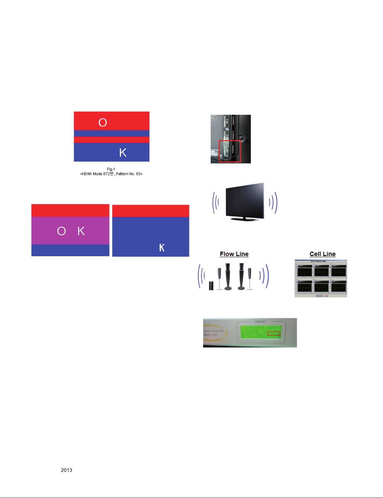
5.4. 3D pattern test
5.4.1. Test equipment
(1) Pattern Generator MSHG-600 or MSPG-6100 (HDMI 1.4
support)
(2) Pattern: HDMI mode (model No. 872, pattern No. 83)
5.5. HDMI ARC Function Inspection
5.5.1. Test equipment
- Optic Receiver Speaker
- MSHG-600 (SW: 1220 ↑)
- HDMI Cable (for 1.4 version)
5.4.2. Test method
(1) Input 3D test signal as Fig.1.
(2) Press ‘OK” key as a 3D input OSD is shown.
(3) Check pattern as Fig2 without 3D glasses. (3D mode
without 3D glasses)
Fig.2 Fig.3
<OK in 3D mode without 3D glasses> <NG in 3D mode without 3D glasses>
5.5.2. Test method
(1) Insert the HDMI Cable to the HDMI ARC port from the
master equipment (HDMI1)
(2) Check the sound from the TV Set
(3) Check the Sound from the Speaker or using AV & Optic
TEST program (It’s connected to MSHG-600)
Only for training and service purposes
* Remark: Inspect in Power Only Mode and check SW version
in a master equipment
5.6. Selection of Country option
Selection of country option is allowed only North American
model (Not allowed Korean model). It is selection of Country
about Rating and Time Zone.
▪ Models: All models which use LJ22E Chassis (See the first
page.)
▪ Press “In-Start” button of Service Remocon, then enter the
“Option” Menu with “PIP CH-“ Button
▪ Select one of these three (USA, CANADA, MEXICO) defends
on its market using “Vol. +/-“button.
- 22 -
LGE Internal Use OnlyCopyright © LG Electronics. Inc. All rights reserved.
Page 23
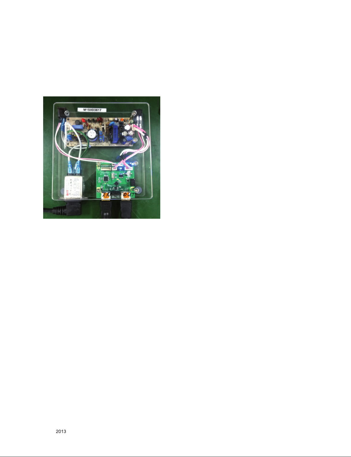
5.7. MHL Test
Step 1) Turn on TV
Step 2) Select HDMI4 mode using input Menu.
Step 3) Set MHL Zig(M1S0D3617) using MHL input, output
and power code.
Step 4) Connect HDMI cable between MHL Zig and HDMI4
port.
Step 5) Check LED light of Zig and Module of Set
Result) If, The LED light is green and The Module shows
normal stream -> OK
Else -> NG
6. GND and HI-POT Testing
6.1. GND & HI-POT auto-check preparation
Check the connection between set and
power cord
(1) Check the POWER CABLE and SIGNAL CABE insertion
condition
6.2. GND & HI-POT auto-check
(1) Pallet moves in the station. (POWER CORD / AV CORD is
tightly inserted)
(2) Connect the AV JACK Tester
(3) Controller (GWS103-4) on.
(4) GND Test (Auto)
- If Test is failed, Buzzer operates.
- If Test is passed, execute next process (Hi-pot test).
(Remove A/V CORD from A/V JACK BOX)
(5) HI-POT test (Auto)
- If Test is failed, Buzzer operates.
- If Test is passed, GOOD Lamp on and move to next process
automatically
6.3. Check Point
(1) Test voltage
3 Poles : GND: 1.5KV/min at 100mA / SIGNAL: 3KV/min at
100mA
(2) TEST time: 1 second
(3) TEST POINT
3 Poles : GND Test = POWER CORD GND and SIGNAL
CABLE GND.
Hi-pot Test = POWER CORD GND and LIVE & NEUTRAL.
(4) LEAKAGE CURRENT: At 0.5mArms
※ Caution : Don’t push The INSTOP KEY after completing the
function inspection.
Only for training and service purposes
- 23 -
LGE Internal Use OnlyCopyright © LG Electronics. Inc. All rights reserved.
Page 24
7. Default Service option
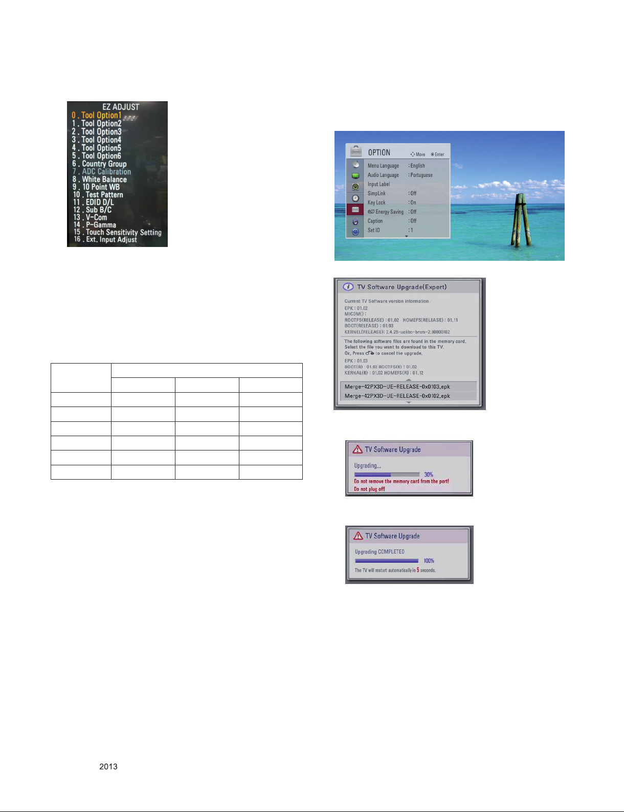
8. USB DOWNLOAD (*.epk file download)
(1) Put the USB Stick to the USB socket
(2) Press Menu key, and move OPTION
(3)
7.1. ADC-Set
▪ R-Gain adjustment Value (default 128)
▪ G-Gain adjustment Value (default 128)
▪ B-Gain adjustment Value (default 128)
▪ R-Offset adjustment Value (default 128)
▪ G-Offset adjustment Value (default 128)
▪ B-Offset adjustment Value (default 128)
7.2. White balance. Value
CENTER (DEFAULT)
C50 0 W50
R Gain 192 192 192
G Gain 192 192 192
B Gain 192 192 192
R Cut 64 64 64
G Cut 64 64 64
B Cut 64 64 64
(4) Press “FAV” Press 7 times.
(5) Select download file (epk file)
Only for training and service purposes
- 24 -
(6) After download is finished, remove the USB stick.
(7) Press “IN-START” key of ADJ remote control, check the
S/W version
LGE Internal Use OnlyCopyright © LG Electronics. Inc. All rights reserved.
Page 25
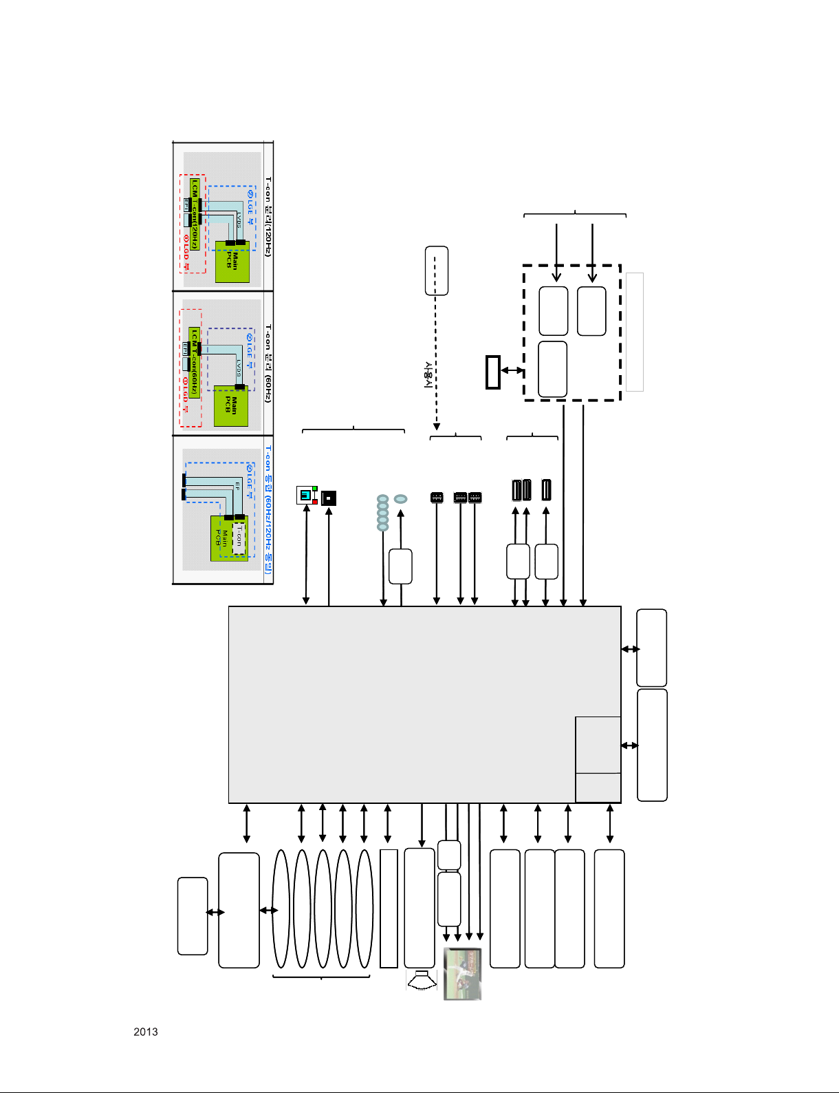
BLOCK DIAGRAM
Audio AMP
(NTP7513)
MTK A2
IF (+/-)
USB1
OPTIC
LAN
DDR3 1600 X 16
(512MB X 2EA)
HDMI1
HDMI2
HDMI3
SYSTEM EEPROM
(256Kb)
HDMI
MUX
Air/
Cable
TUNER
(T/C/A)
TUNER
(S2)
DVB-S
DEMOD
(S2)
LNB
USB2
USB3
41P
51P
eMMC
(4GB)
Sub Micom
(RENESAS
R5F1000G)
DDR3 1600 X 16
(256MB X 1EA)
P_TS
50P
50P
X_TAL
27MHz
T/C/S2 Without ATV
T/C/S2 Without ATV
#EPI & LVDS Diagram
A B
HDCP EEPROM
(16Kb)
X_TAL
32.768KHz
I2S Out
I2C 1
EPI
I2C 2
LVDS
USB
I2C 5
I2C 1
H/P
AV/COMP
Tuner : I2C 6
DVB-S : I2C 4
OCP
2.5A
OCP
1A
(HDD)
MHL 1A
SIL1292
MHL : I2C 4
MHL 사용시
R
E
A
R
S
I
D
E
S
I
D
E
R
E
A
R
(H)
AMP
TI
CVBS/YPbPr
CVBS/RGB
SPDIF OUT
ETHERNET
I2C 3
LOCAL DIMMING
BLUTOOTH
IR
PM
IC
LEVEL
SHIFTER
WIFI
KEY
LOGO LIGHT
SUB
ASSY
I2C 1
UART
IR
KEY
USB_WIFI
Only for training and service purposes
- 25 -
LGE Internal Use OnlyCopyright © LG Electronics. Inc. All rights reserved.
Page 26
1.2V Core
DCDC 6A
3500mA
3.3V Multi
DCDC 4A
2000mA
1.8V TUNER
LDO 1A
240mA
1.25V TUNER
LDO 2A
600mA
24V
12V
3.5VST
640mA
AMP
3230mA
1.5V DDR
LDO 2A
650mA
5V USB
DCDC 5A
3000mA
390mA
WOL/WOW
400mA
MICOM,ETC
15mA
1065mA
730mA
LNB option
LNB
700mA
600mA
1330mA
PANEL
1500mA
45.6W
3.5W
37.9W
Only for training and service purposes
- 26 -
LGE Internal Use OnlyCopyright © LG Electronics. Inc. All rights reserved.
Page 27

24V
5V USB
TPS5450
5A
3000mA
OCP
2CH
OCP
OCP
USB1
USB2
USB3
MHL
NetCast 4.0
Only for training and service purposes
- 27 -
LGE Internal Use OnlyCopyright © LG Electronics. Inc. All rights reserved.
Page 28

12V
1.2V Core
DC DC 6A
5260mA
MTK-A2
NetCast 4.0
MHL
Only for training and service purposes
- 28 -
LGE Internal Use OnlyCopyright © LG Electronics. Inc. All rights reserved.
Page 29
M13
MT5398
[CVBS2P]
Tuner
Jack Side
SoC Side
JK501
COMP1_Y/AV1_CVBS
COMP1_Pb
COMP1_Pr
COMP1/AV1/DVI_L_IN
COMP1/AV1/DVI_R_IN
COMP1_Y/AV1_CVBS_SOC
COMP1_Pb_SOC
[PB0P]
[PR0P]
[AIN4_L_AADC]
COMP1_Pb_SOC
COMP1/AV1/DVI_L_IN_SOC
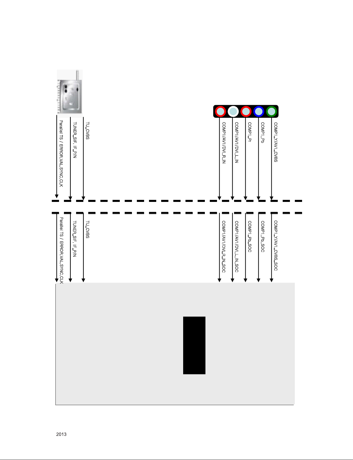
[AIN4_R_AADC]
COMP1/AV1/DVI_R_IN_SOC
TU_CVBS
TUNER_SIF, IF_P/N
[CVBS1P]
[MPXP, ADCINP_DEMOD, ADCINN_DEMOD]
TU_CVBS
TUNER_SIF, IF_P/N
Parallel TS / ERROR,VAL,SYNC,CLK
Parallel TS / ERROR,VAL,SYNC,CLK
Only for training and service purposes
- 29 -
LGE Internal Use OnlyCopyright © LG Electronics. Inc. All rights reserved.
Page 30
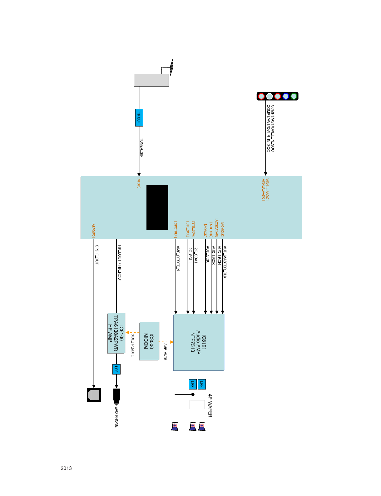
SPDIF_OUT
IC8101
Audio AMP
NTP7513
LPF
COMP1/AV1/DVI_L_IN_SOC
COMP1/AV1/DVI_R_IN_SOC
[ASPDIF0]
Tuner
TR BUF
[MPXP]
AUD_LRCH
HP_LOUT / HP_ROUT
HEAD PHONE
LPF
4P WAFER
[AL0_ADAC]
[AR0_ADAC]
M13
MT5398
TUNER_SIF
[AOLRCK]
[AOSDATA0]
AUD_LRCK
AUD_SCK
[AOBCK]
[STB_SDA]
[STB_SCL]
I2C_SDA1
I2C_SCL1
IC3000
MICOM
AMP_MUTE
[AIN4_L_AADC]
[AIN4_R_AADC]
JK501
AUD_MASTER_CLK
[AOMCLK]
[OPCTRL4]
AMP_RESET_N
IC6100
TPA6138A2PWR
HP AMP
JK3602
JK3700
LPF
SPEAKER_L
SPEAKER_R
WOOFER
(LPF내장)
SIDE_HP_MUTE
Only for training and service purposes
- 30 -
LGE Internal Use OnlyCopyright © LG Electronics. Inc. All rights reserved.
Page 31

HDMI1
HDMI1
HDMI2
HDMI2
HDMI3
HDMI3
CEC_REMOTE
RENESAS
MICOM
HDMI_CEC
MTK A2
Q3001
DDC_SCL_1_SOC
DDC_SCL_2_JACK
DDC_SDA_2_JACK
DDC_SCL_3_JACK
DDC_SDA_3_JACK
TMDS Link 8bits
HDMI_ARC
DDC_SDA_1_SOC
X-tal
32.768kHz
TMDS Link 8bits
TMDS Link 8bits
WOL_CTL
Only for training and service purposes
- 31 -
LGE Internal Use OnlyCopyright © LG Electronics. Inc. All rights reserved.
Page 32

Z_Out
50Pin X 2
PANEL_VCC
(+12V)
PMIC
TPS65178RSL
Level Shift
TPS65198RUYR
EPI CH4 +/-
EPI CH5 +/-
EPI CH6 +/-
VCOM_P
VCOM_N
VCOM_LOOP
VCOM
EPI CH1 +/-
EPI CH2 +/-
EPI CH3 +/-
VCOM_DYN VCOMLFB
VCOMRFB
GMA1/GMA3/GAM9/GMA10/GMA16/GMA18
VDD
VCC
VCC1.8
CLK1_I~CLK6_I
GMA4/GMA5/GAM7/GMA12/GMA14/ GMA15
GMA4/GMA5/GAM7/GMA12/GMA14/GMA15
EO
GST
GCLK
MCLK
EPI_LOCK3
EPI_LOCK6_SOURCEEPI_LOCK6
H_VDD
TR/
Diode
TR/
Diode
SWP
CTRLP
SWN
CTRLN
VGH
VGL
VGL_I
VGH_EVEN/VGH_ODD
VGH_F/VGH_R
6
6
2
2
2
2
2
2
2
2
6
VST
GIP_RST
Only for training and service purposes
- 32 -
LGE Internal Use OnlyCopyright © LG Electronics. Inc. All rights reserved.
Page 33

PMIC
TPS65178RSL
Boost Converter
Buck 1 converter(VCC)
Buck 2 converter(Vcore)
Buck 3 converter(HVdd)
Buck 4 converter(VCC18)
Positive Charge Pump Controller
Negative Charge Pump Controller
6-Ch Gamma Buffer(DAC output)
Vcom reference & gain
Reset
PANEL_VCC
VCC18
VCC
HVdd
Vdd
VCOM_P
VCOM_N
GAM4/5/7/12/14/15
CTRLN
SWP
SWN
CTRLP
VCOM_LOOP
PMIC_RESET
Vcore
Level Shift
TPS65198RUYR
TR/
Diode
TR/
Diode
VGL
VGH
Only for training and service purposes
- 33 -
LGE Internal Use OnlyCopyright © LG Electronics. Inc. All rights reserved.
Page 34

MTK A2
USB1
USB_DP1
USB_DM1
[USB_DP_P2]
[USB_DM_P2]
USB2
USB_DP2
USB_DM2
[GPIO43]
[GPIO46]
OCP
OCP
+5V_USB_1
+5V_USB_2
/USB_OCD1
USB_CTL1
USB_CTL2
/USB_OCD2
USB_WIFI
WIFI_DM
WIFI_DP
Motion Remote
Receiver
Motion Remote
Receiver
M_REMOTE_RX
M_REMOTE_TX
M_RFModule_RESET
[U1RX]
[U1TX]
[OPCTRL49]
[OPCTRL50]
[USB_DM_P3]
[USB_DP_P3]
RENESAS MICOM
[U0TX]
[U0RX]
SOC_TX
SOC_RX
USB_DP3
+5V_USB_3
USB_CTL3
/USB_OCD3
[USB_DM_P1]
[USB_DP_P1]
[GPIO42]
[TCON12]
[USB_DM_P0]
[USB_DP_P0]
USB3
USB_DM3
[GPIO44]
[ADIN2_SRV]
CTS
RTS
[ADIN4_SRV]
4Pin debugging
wafer
Only for training and service purposes
- 34 -
LGE Internal Use OnlyCopyright © LG Electronics. Inc. All rights reserved.
Page 35

521
400
EXPLODED VIEW
Many electrical and mechanical parts in this chassis have special safety-related characteristics. These
parts are identified by in the Schematic Diagram and EXPLODED VIEW.
It is essenti al that these special safet y parts shoul d be replac ed with the same compo nents as
recommended in this manual to prevent X-RADIATION, Shock, Fire, or other Hazards.
Do not modify the original design without permission of manufacturer.
570
Option
IMPORTANT SAFETY NOTICE
LV1
121
540
120
123
122
200
910
530
Option
510
AT1
900
500
A10
Set + Stand
300
Only for training and service purposes
- 35 -
A9
Stand Base+Stand Body
A2
LGE Internal Use OnlyCopyright © LG Electronics. Inc. All rights reserved.
Page 36

EAX64797001* : LD33B
Copyright ⓒ 2013 LG Electronics. Inc. All right reserved.
Only for training and service purposes
LGE Internal Use Only
EAX64872101* : LA33B
IC100-*2
R1EX24256BSAS0A
A0
1
A1
2
A2
3
VSS
4
NVRAM_RENESAS
I2C_SCL5
I2C_SDA5
VCC
8
WP
7
SCL
6
SDA
5
+3.3V_NORMAL
R101
4.7K
R100
4.7K
OPT
R102
AT24C256C-SSHL-T
4.7K
OPT
A0
A1
A2
GND
NVRAM
IC100
1
2
3
4
NVRAM_ATMEL
IC100-*1
M24256-BRMN6TP
E0
VCC
1
8
WC
E1
7
2
SCL
E2
6
3
SDA
+3.3V_NORMAL
VCC
8
WP
7
SCL
6
SDA
5
VSS
5
4
NVRAM_ST
Write Protection
- Low : Normal Operation
- High : Write Protection
R135 33
R134 33
HDCP EEPROM
OPT
IC101
M24C16-R
NC_1
NC_2
NC_3
VSS
VCC
8
1
WC
2
7
SCL
3
6
SDA
4
5
I2C
R121
1.2K
+3.3V_NORMAL
R105
4.7K
Country_TW
R103
4.7K
NON_Country_TW
R120 33
R115 33
R116 33
R117 33
R118 33
R119 33
R110 33
R111 33
R112 33
R113 33
R114 33
R109 33
R106
4.7K
MTK_FHD
FRC_120Hz
R104
4.7K
MTK_HD
NON_FRC_60Hz
STB_SCL
STB_SDA
OPCTRL_11_SCL
OPCTRL_10_SDA
OSCL1
OSDA1
OSCL2
OSDA2
OSCL0
OSDA0
OPCTRL_1_SCL
OPCTRL_0_SDA
THE SYMBOL MARK OF THIS SCHEMETIC DIAGRAM INCORPORATES
SPECIAL FEATURES IMPORTANT FOR PROTECTION FROM X-RADIATION.
FILRE AND ELECTRICAL SHOCK HAZARDS, WHEN SERVICING IF IS
ESSENTIAL THAT ONLY MANUFATURES SPECFIED PARTS BE USED FOR
THE CRITICAL COMPONENTS IN THE SYMBOL MARK OF THE SCHEMETIC.
+3.3V_NORMAL
OPT
C100
0.1uF
16V
R125 4.7K
OPT
R126 22
OPT
R127 22
OPT
R132
R124
1.2K
2.7K
R133
2.7K
Model Option
R130
4.7K
R108
4.7K
R107
4.7K
Non_Country_AJJA
R123
4.7K
Country_AJJA
R122
4.7K
MODULE_V13
R128
4.7K
MODULE_V12
R131
MTK_DDR_1.25GB
R129
MTK_DDR_1.5GB
4.7K
4.7K
R138
2.7K
I2C_SCL1
I2C_SDA1
R141
2.7K
R137
4.7K
MTK_CP_BOX
MTK_DVB_T2_TUNER
R136
4.7K
MTK_NON_CP_BOX
MTK_NON_DVB_T2_TUNER
+3.3V_NORMAL
R155
1K
R154
1K
I2C_1 : AMP, L/DIMMING,HDCP KEY
I2C_2 : T-CON,
I2C_3 : MICOM
I2C_4 : S/Demod,T2/Demod, LNB, MHL(Sil1292)
I2C_5 : NVRAM
I2C_6 : TUNER_MOPLL(T/C,ATV)
+3.3V_NORMAL
R147
R142
2.7K
R140
R139
4.7K
4.7K
R150
2.7K
2.7K
R145
4.7K
R146
4.7K
MTK_EPI
DDR_0.78G
MTK_DVB_S_TUNER
R143
4.7K
R144
4.7K
MTK_NON_EPI
NON_DDR_0.78G
MTK_NON_DVB_S_TUNER
R149
R148
R151
2.7K
4.7K
4.7K
R152
2.7K
NON_TU_Q_KR
NON_TU_Q_KR
R153
2.7K
MODEL_OPT_0
MODEL_OPT_1
MODEL_OPT_2
MODEL_OPT_3
/S2_RESET
MODEL_OPT_5
MODEL_OPT_6
MODEL_OPT_7
MODEL_OPT_8
MODEL_OPT_9
MODEL_OPT_10
OPT
TU_Q_KR
TU_N_TW/BR
MODEL_OPT_4
R157
OPT
1K
R156
1K
R152-*1
1.5K
R152-*2
TU_N_TW/BR
1.2K
I2C_SCL1
I2C_SDA1
I2C_SCL2
I2C_SDA2
I2C_SCL_MICOM
I2C_SDA_MICOM
I2C_SCL4
I2C_SDA4
I2C_SCL5
I2C_SDA5
I2C_SCL6
I2C_SDA6
TU_Q_KR
OPT
R153-*1
1.5K
R153-*2
1.2K
R162
1K
R160
OPT
1K
MODEL_OPT_1
MODEL_OPT_2
MODEL_OPT_3
MODEL_OPT_4
MODEL_OPT_5
MODEL_OPT_6
MODEL_OPT_7
MODEL_OPT_8
MODEL_OPT_9
MODEL_OPT_10
MODEL_OPT_5
MODEL_OPT_9
STRAPPING LED_PWM0 LED_PWM1 OPCTRL3 OPCTRL7
ICE mode + 27M + serial boot 1 0 0 0
ICE mode + 27M + ROM to Nand boot 1 0 0 1
ICE mode + 27M + ROM to 60bit ECC Nand boot 1 0 1 0
ICE mode + 27M + ROM to eMMC boot from 1 0 1 1
EMMC pins (share pins w/s NAND)
R163
1K
R161
1K
ICE mode + 27M + ROM to eMMC 1 1 0 0
Boot from SDIO pins
LED_PWM0
LED_PWM1
OPCTRL3
OPCTRL7
Country_TW
FRC
FRC(120Hz)
Panel
Country_AJJA
Module
DDR_1.25G
DDR
CP BOX
T2 Tuner
Support
Support
S Tuner
DDR
DDR_0.78G
Support
EPI
DDR_1.25G DDR_1.5G DDR_0.768G
High
Low
TW
FHD
AJJA
Enable
Low
Low
LOWHIGH
Non_TWMODEL_OPT_0
No FRC(60Hz)
HD
Non_AJJA
V12V13
DDR_1.5G
Disable
Not Support
Not Support
NON_DDR_0.78G
Not Support
High
High
SOC -> CI SLOT
MT5398_MCLKI
MT5398_MIVAL_ERR
MT5398_MISTRT
SOC -> CI SLOT
MT5398_TS_OUT[0-7]
CI_DATA[0-7]
GPIO45(EMMC_RST) is dedicated to reset
EMMC for improving A1’s leakage current
/USB_OCD2
/USB_OCD1
/USB_OCD3
EMMC_RST
USB_CTL1
#SIL_RESET
USB_CTL3
Close to eMMC Flash
(IC8100)
EMMC_CLK
CI_ADDR[0-14]
CI_DATA[0]
CI_DATA[1]
CI_DATA[2]
CI_DATA[3]
CI_DATA[4]
CI_DATA[5]
CI_DATA[6]
CI_DATA[7]
CI SLOT -> SOC
SC_ID_SOC
R169
R170
MODEL_OPT_4
CI_ADDR[0-14]
MT5398_TS_OUT[0]
MT5398_TS_OUT[1]
MT5398_TS_OUT[2]
MT5398_TS_OUT[3]
MT5398_TS_OUT[4]
MT5398_TS_OUT[5]
MT5398_TS_OUT[6]
MT5398_TS_OUT[7]
MT5398_TS_IN[0]
MT5398_TS_IN[1]
MT5398_TS_IN[2]
MT5398_TS_IN[3]
MT5398_TS_IN[4]
MT5398_TS_IN[5]
MT5398_TS_IN[6]
MT5398_TS_IN[7]
NON_EU
10K
10K
MODEL_OPT_0
M_RFModule_RESET
OPC_EN
/TU_RESET1
/S2_RESET
R168
10K
VDD3V3
R194
CI_ADDR[0]
CI_ADDR[1]
CI_ADDR[2]
CI_ADDR[3]
CI_ADDR[4]
CI_ADDR[5]
CI_ADDR[6]
CI_ADDR[7]
CI_ADDR[8]
CI_ADDR[9]
CI_ADDR[10]
CI_ADDR[11]
CI_ADDR[12]
CI_ADDR[13]
CI_ADDR[14]
EPI_LOCK6
OTP_WRITE
MODEL_OPT_3
MODEL_OPT_7
MODEL_OPT_5
MODEL_OPT_6
X-TAL
MT5398_XTAL_IN
L/DIM0_MOSI
R195
10K
10K
L/DIM0_SCLK
L/DIM0_VS
OSDA0
OSCL0
OSDA1
OSCL1
AVDD_33SB
AVDD_33SB
VDD3V3
CTS
RTS
AJ23
AH23
AE28
AD28
AF22
AK21
AG24
AM18
MT5398_XTAL_IN
MT5398_XTAL_OUT
C111
0.1uF
C110
0.1uF
C109
0.1uF
C107
4.7uF
10V
IC105
LGE2122[A2_M13]
B30
GPIO0
A31
GPIO1
B31
GPIO2
A32
GPIO3
C30
GPIO4
A33
GPIO5
B32
GPIO6
C31
GPIO7
E30
GPIO8
F29
GPIO9
F27
GPIO10
F28
GPIO11
C32
GPIO12
F30
GPIO13
F32
GPIO14
D30
GPIO15
D32
GPIO16
F31
GPIO17
F33
GPIO18
E31
GPIO19
E32
GPIO20
D31
GPIO21
D33
GPIO22
E29
GPIO23
C33
GPIO24
B33
GPIO25
A30
GPIO26
E28
GPIO27
C29
GPIO28
J28
GPIO29
H29
GPIO30
J26
GPIO31
G30
GPIO32
G27
GPIO33
E27
GPIO34
D29
GPIO35
D28
GPIO36
H28
GPIO37
J27
GPIO38
G29
GPIO39
G31
GPIO40
G28
GPIO41
B28
GPIO42
K28
GPIO43
E25
GPIO44
D21
GPIO45
G23
GPIO46
C28
GPIO47
F24
GPIO48
AB8
GPIO49
AA7
GPIO50
AD6
GPIO51
AC8
GPIO52
AC7
GPIO53
AB6
GPIO54
AC6
GPIO55
ADIN0_SRV
ADIN1_SRV
ADIN2_SRV
ADIN3_SRV
ADIN4_SRV
ADIN5_SRV
ADIN6_SRV
ADIN7_SRV
C112
4.7uF
10V
DEMOD_RST
DEMOD_TSCLK
DEMOD_TSDATA0
DEMOD_TSDATA1
DEMOD_TSDATA2
DEMOD_TSDATA3
DEMOD_TSDATA4
DEMOD_TSDATA5
DEMOD_TSDATA6
DEMOD_TSDATA7
DEMOD_TSSYNC
DEMOD_TSVAL
CI_INT
CI_TSCLK
CI_TSDATA0
CI_TSSYNC
CI_TSVAL
PVR_TSCLK
PVR_TSVAL
PVR_TSSYNC
PVR_TSDATA0
PVR_TSDATA1
SPI_CLK1
SPI_CLK
SPI_DATA
SPI_CLE
OPWM2
OPWM1
OPWM0
SD_D0
SD_D1
SD_D2
SD_D3
SD_CMD
SD_CLK
LED_PWM1
LED_PWM0
OPCTRL11
OPCTRL10
OPCTRL9
OPCTRL8
OPCTRL7
OPCTRL6
OPCTRL5
OPCTRL4
OPCTRL3
OPCTRL2
OPCTRL1
OPCTRL0
C114
1.0pF
DVB_1pF
50V
C114-*1
2.7pF
50V
ATSC_2.7pF
LGE2122[A2_M13]
AK10
JTCK
AK11
JTDI
AL9
JTDO
AJ11
JTMS
AJ12
JTRST
AH11
OSDA0
AH10
OSCL0
AF11
OSDA1
AG11
OSCL1
AN29
XTALI
AM29
XTALO
AN30
AVDD33_XTAL_STB
AL29
AVSS33_XTAL_STB
AN17
AVDD33_VGA_STB
AL17
AVSS33_AVSS33_VGA_STB
AL26
AVDD33_PLL
AC21
AVSS33_PLLGP
H21
AVSS33_CPUPLL
AM17
AVDD10_LDO
AN16
AVDD10_ELDO
P30
N32
R27
T26
T27
P26
R28
U27
U26
R26
R29
P27
L25
N33
K26
N30
N31
M31
M27
L27
M29
M30
L30
L33
L32
K27
AL8
AM8
AM9
D27
C27
D26
C26
A28
E24
AF15
AG15
AL16
AM16
AE17
AG19
AH17
AE19
AH19
AK16
AG17
AJ17
AF19
AJ19
X100
27MHz
X-TAL_1
GND_1
GND_2
4
1
X-TAL_2
2
3
IC105
Wake On Lan
EMMC_CLK
PCM_RST
FE_DEMOD1_TS_CLK
FE_DEMOD1_TS_SYNC
FE_DEMOD1_TS_VAL
/PCM_REG
/PCM_CE1
MT5398_TS_SYNC
/PCM_WE
/PCM_OE
MT5398_TS_VAL
CI_A_VS1
MT5398_TS_CLK
/PCM_IRQA
/PCM_WAIT
/CI_CD2
/CI_CD1
/PCM_IORD
/PCM_IOWR
+3.3V_NORMAL
/RST_HUB
SMARTCARD_CLK/SD_EMMC_DATA[0]
SMARTCARD_PWR_SEL/SD_EMMC_DATA[1]
SMARTCARD_RST/SD_EMMC_DATA[2]
SMARTCARD_DET/SD_EMMC_DATA[3]
SMARTCARD_VCC/SD_EMMC_CMD
SMARTCARD_DATA/SD_EMMC_CLK
LED_PWM1
LED_PWM0
5V Tolerance
OPCTRL_11_SCL
OPCTRL_10_SDA
COMP1_DET
SC_DET
OPCTRL7
HP_DET
AV1_CVBS_DET
AMP_RESET_SOC
OPCTRL3
RF_SWITCH_CTL
OPCTRL_1_SCL
OPCTRL_0_SDA
MID_MAIN_1
C115
1.0pF
50V
DVB_1pF
AH15
U0TX
AH14
U0RX
AH13
U1TX
AG13
U1RX
D24
POWE
B25
POOE
D25
POCE1
A25
POCE0
C22
PDD7
B22
PDD6
A22
PDD5
C23
PDD4
A23
PDD3
B23
PDD2
D23
PDD1
C24
PDD0
C25
PARB
A26
PACLE
B26
PAALE
C21
AL15
OPWRSB
AK20
ORESET
AF17
OIRI
C20
FSRC_WR
AL14
STB_SCL
AK15
STB_SDA
AE14
POR_BND
FE_DEMOD1_TS_DATA[0]
FE_DEMOD1_TS_DATA[1]
FE_DEMOD1_TS_DATA[2]
FE_DEMOD1_TS_DATA[3]
FE_DEMOD1_TS_DATA[4]
FE_DEMOD1_TS_DATA[5]
FE_DEMOD1_TS_DATA[6]
FE_DEMOD1_TS_DATA[7]
CI SLOT -> SOC
CI SLOT -> SOC
CI SLOT -> SOC
R174
4.7K
OPT
R173
1K
PWM1_PULL_DOWN_1K
MT5398_XTAL_OUT
C115-*1
2.7pF
50V
ATSC_2.7pF
EMMC_DATA[7]
EMMC_DATA[6]
EMMC_DATA[5]
EMMC_DATA[4]
EMMC_DATA[3]
EMMC_DATA[2]
R193 4.7K
R177
4.7K
OPT
PWM_DIM2
R179
22
22
R178
R176
1K
PWM2_PULL_DOWN_1K
AMP_RESET_SOC
+3.3V_NORMAL
SOC_TX
R183
SOC_RX
4.7K
EMMC_CMD
FE_LNA_Ctrl1
FE_LNA_Ctrl2
CAM_SLIDE_DET
EMMC_DATA[1]
EMMC_DATA[0]
EMMC_CLK
R158
22
STB_SCL
STB_SDA
FE_DEMOD1_TS_DATA[0-7]
D100
1N4148W
100V
4.7K
R180
EXTERNAL DEMOD
-> SOC
PWM_DIM2
PWM_DIM1
SMARTCARD_CLK/SD_EMMC_DATA[0]
SMARTCARD_PWR_SEL/SD_EMMC_DATA[1]
SMARTCARD_RST/SD_EMMC_DATA[2]
SMARTCARD_DET/SD_EMMC_DATA[3]
SMARTCARD_VCC/SD_EMMC_CMD
SMARTCARD_DATA/SD_EMMC_CLK
R182
R184
4.7K
33
EMMC_DATA[2-7]
AVDD_33SB
R188
4.7K
R187
4.7K
OPT
R186
R196
240
R185
10K
2011.12.13
M_REMOTE_TX
M_REMOTE_RX
CAM_SLIDE_DET
WOL/ETH_POWER_ON
+3.3V_NORMAL
22
Q100
PMV48XP
D
G
AMP_RESET_N
R189
10K
OPT
C117
0.1uF
16V
+3.3V_NORMAL
S
OTP_WRITE
/RST_HUB
SOC_RESET
10K
R190
8
Page 37

PLACE AT JACK SIDE
Copyright ⓒ 2013 LG Electronics. Inc. All right reserved.
Only for training and service purposes
LGE Internal Use Only
Port was changed !!!!
WIFI_DP
WIFI_DM
+1.2V_MTK_AVDD
VDD3V3_HDMI
C398
5pF
50V
WIFI_EMI
DDC_SCL_3_JACK
DDC_SCL_1_SOC
DDC_SDA_3_JACK
DDC_SDA_1_SOC
5V_HDMI_3_JACK
5V_HDMI_1_SOC
HDMI_HPD_3_JACK
HDMI_HPD_1_SOC
HDMI_HPD_4_MHL
C303
0.1uF
C399
5pF
50V
WIFI_EMI
ARC
TP381
HDMI_CEC
DDC_SCL_MHL
DDC_SDA_MHL
R305
1K
R306
1K
R307 1K
5VBUS
C306
0.1uF
C307
C304
0.1uF
0.1uF
USB_DP3
USB_DM3
USB_DP2
USB_DM2
USB_DP1
USB_DM1
R382
0
0
R383
VDD3V3
C302
0.1uF
HP_LOUT_AMP
HP_ROUT_AMP
Place at JACK SIDE
V26
AC27
AB27
AA26
W27
AC26
AB26
Y26
W26
AE29
Y27
AA28
V28
AD29
AA27
AA29
V29
AA33
AA32
P33
P32
AH33
AE27
T25
W25
AD27
H32
H33
J32
J31
K32
K31
AN10
AM10
K33
AN8
M25
AE11
R302
180
R303
82
LGE2122[A2_M13]
HDMI_CEC
HDMI_0_SCL
HDMI_1_SCL
HDMI_2_SCL
HDMI_3_SCL
HDMI_0_SDA
HDMI_1_SDA
HDMI_2_SDA
HDMI_3_SDA
HDMI_0_PWR5V
HDMI_1_PWR5V
HDMI_2_PWR5V
HDMI_3_PWR5V
HDMI_0_HPD
HDMI_1_HPD
HDMI_2_HPD
HDMI_3_HPD
AVDD12_HDMI_0_RX
AVDD12_HDMI_1_RX
AVDD12_HDMI_2_RX
AVDD12_HDMI_3_RX
AVDD33_HDMI
AVSS33_HDMI_RX_1
AVSS33_HDMI_RX_2
AVSS33_HDMI_RX_3
AVSS33_HDMI_RX_4
LGE2122[A2_M13]
USB_DP_P0
USB_DM_P0
USB_DP_P1
USB_DM_P1
USB_DP_P2
USB_DM_P2
USB_DP_P3
USB_DM_P3
AVDD33_USB_P0P1P2
AVDD33_USB_P3
AVSS33_USB_P1
AVSS33_USB_P3
HP_OUT
L303
BLM18PG121SN1D
HP_OUT
L302
BLM18PG121SN1D
C311 1uF
IC105
IC105
HP_OUT
C332
0.22uF
10V
HP_OUT
C331
0.22uF
10V
+5V_NORMAL
10V
HDMI_0_RX_0
HDMI_0_RX_0B
HDMI_0_RX_1
HDMI_0_RX_1B
HDMI_0_RX_2
HDMI_0_RX_2B
HDMI_0_RX_C
HDMI_0_RX_CB
HDMI_1_RX_0
HDMI_1_RX_0B
HDMI_1_RX_1
HDMI_1_RX_1B
HDMI_1_RX_2
HDMI_1_RX_2B
HDMI_1_RX_C
HDMI_1_RX_CB
HDMI_2_RX_0
HDMI_2_RX_0B
HDMI_2_RX_1
HDMI_2_RX_1B
HDMI_2_RX_2
HDMI_2_RX_2B
HDMI_2_RX_C
HDMI_2_RX_CB
HDMI_3_RX_0
HDMI_3_RX_0B
HDMI_3_RX_1
HDMI_3_RX_1B
HDMI_3_RX_2
HDMI_3_RX_2B
HDMI_3_RX_C
HDMI_3_RX_CB
Wake On Lan
HP_ROUT
R308
1.2K
OPT
R309
100K
TXVP_0
TXVN_0
RXVP_1
RXVN_1
PHYLED1
PHYLED0
AVDD33_ETH
AVSS33_ELDO
AVSS33_LD
AVSS33_COM
HP_LOUT
Close to JACK
C345
10uF
COMP1/AV1/DVI_L_IN
HDMI_ARC
COMP1/AV1/DVI_R_IN
AG30
AG31
AF30
AF31
AE32
AE33
AG32
AG33
AD30
AD31
AC32
AC33
AC30
AC31
AE30
AE31
Y30
Y31
W32
W33
W30
W31
AA30
AA31
U30
U31
T32
T33
T30
T31
V30
V31
AL13
AM13
AL12
AM12
AF13
AJ13
AN12
REXT
AN14
AE13
AC16
AC15
AVDD_33SB
D0+_HDMI3_JACK
D0-_HDMI3_JACK
D1+_HDMI3_JACK
D1-_HDMI3_JACK
D2+_HDMI3_JACK
D2-_HDMI3_JACK
CK+_HDMI3_JACK
CK-_HDMI3_JACK
D0+_HDMI1_SOC
D0-_HDMI1_SOC
D1+_HDMI1_SOC
D1-_HDMI1_SOC
D2+_HDMI1_SOC
D2-_HDMI1_SOC
CK+_HDMI1_SOC
CK-_HDMI1_SOC
D0+_HDMI4_MHL
D0-_HDMI4_MHL
D1+_HDMI4_MHL
D1-_HDMI4_MHL
D2+_HDMI4_MHL
D2-_HDMI4_MHL
CK+_HDMI4_MHL
CK-_HDMI4_MHL
C328
0.1uF
EPHY_TDP
EPHY_TDN
EPHY_RDP
EPHY_RDN
MODEL_OPT_1
/TU_RESET2
R31524K
Close to Tuner
TU_S/N/Q_T/US/KR/TW
IF_P
TU_S/N/Q_T/US/KR/TW
IF_N
+1.2V_MTK_AVDD
C350
C354
VDD3V3
0.1uF
0.1uF
C347
0.1uF
For PCB Pattern
SC_R_IN_SOC
SC_L_IN_SOC
TP379
PC_R_IN_SOC
TP380
PC_L_IN_SOC
COMP1/AV1/DVI_R_IN_SOC
COMP1/AV1/DVI_L_IN_SOC
Close to AVDD33_ADAC & AVDD33_AADC
VDD3V3
L304
C365
C305
C362
10uF
1uF
0.1uF
10V
+1.2V_MTK_AVDD
SC_CVBS_IN_SOC
COMP1_Y/AV1_CVBS_SOC
TU_CVBS
10V
R339
2.2K
OPT
C351
0.1uF
C352 0.01uF
TU_A_GLOBAL_6/7
R341 100
R340 100
TU_A_GLOBAL_6/7
TUNER_SIF
Close to MT5369
TU_S/N/Q_T/US/KR/TW
C312
R346
1K
R331
R380
1K
1K
TU_S/N/Q_T/US/KR/TW
C336
1uF
10V
TU_S/N/Q_T/US/KR/TW
C337 1uF
10V
TU_S/N/Q_T/US/KR/TW
TU_S/N/Q_T/US/KR/TW
IF_AGC
33pF
TU_S/N/Q_T/US/KR/TW
TU_S/N/Q_T/US/KR/TW
C310
33pF
TU_S/N/Q_T/US/KR/TW
R332 10K
C341
0.047uF
TU_S/N/Q_T/US/KR/TW
For PCB Pattern
R334 51
R335 51
Close to Tuner
MODEL_OPT_2
R343
24K
1%
AVDD3V3_AADC
C358
0.1uF
VDD3V3
TU_S/N/Q_T/US/KR/TW
R342 10K
C355
0.047uF
TU_S/N/Q_T/US/KR/TW
Close to MT5369
R328
470K
OPT
R329
470K
OPT
MODEL_OPT_8
MODEL_OPT_9
MODEL_OPT_10
GCLK_SOC
MCLK_SOC
GST_SOC
EO_SOC
VCOM_DYN
PMIC_RESET
2D/3D_CTL
PCM_5V_CTL
USB_CTL2
C363
1uF
10V
C364
0.1uF
TP300
OSCL2
OSDA2
C360 0.047uF
C359 0.047uF
TU_A_GLOBAL_6/7
C361 1uF
VDD3V3
AVDD3V3_AADC
Near the SOC
C338
560pF
50V
OPT
C339
560pF
50V
OPT
LGE2122[A2_M13]
AA8
TCON0
AA9
TCON1
W6
TCON2
U6
TCON3
U7
TCON4
V8
TCON5
V6
TCON6
AB7
TCON7
W9
TCON8
U8
TCON9
U9
TCON10
V9
TCON11
V7
TCON12
AN1
AVDD12_LVDS_1
AN2
AVDD12_LVDS_2
AN3
AVDD12_LVDS_3
AN4
AVDD33_LVDS
AM4
AVSS12_LVDS_1
AM3
AVSS12_LVDS_2
AF5
AVSS12_LVDS_3
AE5
AVSS33_LVDS_1
AC5
AVSS33_LVDS_2
V5
AVSS33_LVDS_3
T1
REXT_VPLL
LGE2122[A2_M13]
AL32
AIN1_R_AADC
AN32
AIN1_L_AADC
AM33
AIN2_R_AADC
AM31
AIN2_L_AADC
AM32
AIN3_R_AADC
AK33
AIN3_L_AADC
AL33
AIN4_R_AADC
AN33
AIN4_L_AADC
AJ32
AVDD33_AADC
AC24
AVSS33_AADC
AN31
VMID_AADC
AH25
MPXP
LGE2122[A2_M13]
AM27
ADCINP_DEMOD
AN27
ADCINN_DEMOD
AN26
AVDD33_DEMOD
AN28
AVDD12_DEMOD
AL28
AVSS33_DEMOD
AL27
AVSS12_DEMOD
L26
IF_AGC
M28
RF_AGC
AJ27
LOUTN
AK27
LOUTP
N27
OSCL2
N26
OSDA2
AK26
CVBS3P
AM25
CVBS2P
AH26
CVBS1P
AK25
CVBS0P
AJ26
CVBS_COM
AM26
AVDD33_CVBS
AB20
AVSS33_CVBS_1
AB22
AVSS33_CVBS_2
16V
C346
10uF
16V
IC105
IC105
IC105
1608 sizs For EMI
R344
1608 sizs For EMI
R345
BE0P
BE0N
BE1P
BE1N
BE2P
BE2N
BECKP
BECKN
BE3P
BE3N
BE4P
BE4N
BO0P
BO0N
BO1P
BO1N
BO2P
BO2N
BOCKP
BOCKN
BO3P
BO3N
BO4P
BO4N
AE0P
AE0N
AE1P
AE1N
AE2P
AE2N
AECKP
AECKN
AE3P
AE3N
AE4P
AE4N
AO0P
AO0N
AO1P
AO1N
AO2P
AO2N
AOCKP
AOCKN
AO3P
AO3N
AO4P
AO4N
AR0_ADAC
AL0_ADAC
AR1_ADAC
AL1_ADAC
AR2_ADAC
AL2_ADAC
AVDD33_ADAC
AVSS33_ADAC
ALIN
ASPDIF0
ASPDIF1
AOBCK
AOLRCK
AOMCLK
AOSDATA4
AOSDATA3
AOSDATA2
AOSDATA1
AOSDATA0
VGA_SDA
VGA_SCL
VDACX_OUT
VDACY_OUT
AVDD33_VIDEO
AVDD12_RGB
AVSS33_VDAC_BG
AVSS12_RGB
AVSS33_VDAC
Close to Main Chip
30K
C342
100pF
50V
30K
C343
100pF
50V
Y1
TXC4N
Y2
TXC4P
W3
TXC3N
W4
TXC3P
V3
TXCCLKN
V4
TXCCLKP
V1
TXC2N
V2
TXC2P
U3
TXC1N
U4
TXC1P
T3
TXC0N
T4
TXC0P
AD1
TXD4N
AD2
TXD4P
AC3
TXD3N
AC4
TXD3P
AB3
TXDCLKN
AB4
TXDCLKP
AB1
TXD2N
AB2
TXD2P
AA3
TXD1N
AA4
TXD1P
Y3
TXD0N
Y4
TXD0P
AH1
TXA4N
AH2
TXA4P
AG3
TXA3N
AG4
TXA3P
AF3
TXACLKN
AF4
TXACLKP
AF1
TXA2N
AF2
TXA2P
AE3
TXA1N
AE4
TXA1P
AD3
TXA0N
AD4
TXA0P
AM1
TXB4N
AM2
TXB4P
AL3
TXB3N
AL4
TXB3P
AK3
TXBCLKN
AK4
TXBCLKP
AK1
TXB2N
AK2
TXB2P
AJ3
TXB1N
AJ4
TXB1P
AH3
TXB0N
AH4
TXB0P
AK30
AJ29
AJ31
AK29
AJ30
Ready For commercial Audio_R_OUT
AH28
Ready For commercial Audio_L_OUT
AJ33
AC23
AG9
AG10
V27
AK9
AJ9
AF10
AH9
AK8
AJ8
AH8
AJ10
AK18
HSYNC
AL18
VSYNC
AL20
RP
AM20
GP
AL19
BP
AN20
COM
AK19
SOG
AG22
AH22
AL21
COM1
AK22
PB1P
AL22
PR1P
AM21
Y1P
AN21
SOY1
AM23
COM0
AL23
PB0P
AL24
PR0P
AN23
Y0P
AK23
SOY0
AH24
AJ24
AN25
AN18
AC19
AK17
AE20
COMP1/AV1/DVI_L_IN_SOC
COMP1/AV1/DVI_R_IN_SOC
AVDD3V3_AADC
Don’t use as GPIO
C3710.01uF
C3720.01uF
C3730.01uF
C3740.01uF
C3751500pF
OPT
R3490
R35010
EU
VDD3V3
TP376
TP305
TP303
TP306
TP304
TP382
TP383
TP301
TP302
R36151
R36251
R36351
R36451
DTV/MNT_V_OUT_SOC
+1.2V_MTK_AVDD
C382
0.1uF
HP_OUT
HP_OUT
R3511.2K
R3521.2K
COMP1_Y/AV1_CVBS
C377
C383
1200pF
1200pF
HP_OUT
HP_OUT
SPDIF_OUT
ARC
SC_COM_SOC
SC_G_SOC
SC_R_SOC
SC_B_SOC
SC_FB_SOC
For PCB Pattern
COMP1_COM_SOC
COMP1_Pb_SOC
COMP1_Pr_SOC
COMP1_Y/AV1_CVBS_SOC
COMP1_Pb
COMP1_Pr
1.0Vpp
HP_OUT
HP_OUT
R3691.2K
R3701.2K
ZD302
ZD304
ZD306
C390
1200pF
HP_OUT
R366 100
R367 100
R368 100
R371 100
PCB_700*
ADLC 5S 02 015
PCB_700*
ADLC 5S 02 015
ADLC 5S 02 015
C395
1200pF
HP_OUT
1608 sizs For EMI
0
R374
C388
C394
27pF
27pF
50V
50V
OPT
OPT
1608 sizs For EMI
0
R373
C391
C386
27pF
27pF
50V
50V
OPT
OPT
1608 sizs For EMI
0
R372
C385
C392
27pF
27pF
50V
50V
FOR EMI
OPT
OPT
For PCB Pattern
HP_ROUT_MAIN
HP_LOUT_MAIN
SCART_Rout_SOC
SCART_Lout_SOC
AUD_SCK
AUD_LRCK
AUD_MASTER_CLK
C387
C389
C393
22pF
22pF
22pF
OPT
OPT
OPT
AUD_LRCH
C396
33pF
OPT
C384
R355
10pF
75
50V
R381
1%
0
1/16W
R354
C379
75
10pF
50V
1%
C378
R353
75
10pF
50V
1%
COMP1_Y/AV1_CVBS_SOC
COMP1_COM_SOC
COMP1_Pb_SOC
COMP1_Pr_SOC
MT5398_MCLKI
MT5398_MIVAL_ERR
MT5398_MISTRT
MT5398_TS_OUT[0-7]
CI_DATA[0-7]
CI_ADDR[0-14]
CI_DATA[0]
CI_DATA[1]
CI_DATA[2]
CI_DATA[3]
CI_DATA[4]
CI_DATA[5]
CI_DATA[6]
CI_DATA[7]
MT5398_TS_OUT[0]
MT5398_TS_OUT[1]
MT5398_TS_OUT[2]
MT5398_TS_OUT[3]
MT5398_TS_OUT[4]
MT5398_TS_OUT[5]
MT5398_TS_OUT[6]
MT5398_TS_OUT[7]
MT5398_TS_IN[0]
MT5398_TS_IN[1]
MT5398_TS_IN[2]
MT5398_TS_IN[3]
MT5398_TS_IN[4]
MT5398_TS_IN[5]
MT5398_TS_IN[6]
MT5398_TS_IN[7]
SC_ID_SOC
/CI_CD2
/CI_CD1
/PCM_IORD
/PCM_IOWR
PCM_RST
/PCM_REG
/PCM_CE1
MT5398_TS_SYNC
/PCM_WE
/PCM_OE
MT5398_TS_VAL
CI_A_VS1
MT5398_TS_CLK
/PCM_IRQA
/PCM_WAIT
SC_R_IN_SOC
SC_L_IN_SOC
SC_CVBS_IN_SOC
SC_COM_SOC
SC_G_SOC
SC_R_SOC
SC_B_SOC
SC_FB_SOC
DTV/MNT_V_OUT_SOC
SCART_Rout_SOC
SCART_Lout_SOC
PCM_5V_CTL
SC_DET
CI_ADDR[0]
CI_ADDR[1]
CI_ADDR[2]
CI_ADDR[3]
CI_ADDR[4]
CI_ADDR[5]
CI_ADDR[6]
CI_ADDR[7]
CI_ADDR[8]
CI_ADDR[9]
CI_ADDR[10]
CI_ADDR[11]
CI_ADDR[12]
CI_ADDR[13]
CI_ADDR[14]
TP312
TP313
TP314
TP315
TP316
TP317
TP318
TP319
TP320
TP321
TP322
TP323
TP324
TP325
TP326
TP327
TP328
TP329
TP330
TP331
TP332
TP333
TP334
TP335
TP336
TP337
TP338
TP339
TP340
TP341
TP342
TP343
TP344
TP345
TP346
TP347
TP348
TP349
TP350
TP351
TP352
TP353
TP354
TP355
TP356
TP357
TP358
TP307
TP308
TP309
TP310
TP311
TP359
TP360
TP361
TP362
TP363
TP364
TP365
TP366
TP367
TP368
TP369
TP370
TP371
TP372
TP373
TP374
TP375
TP377
TP378
THE SYMBOL MARK OF THIS SCHEMETIC DIAGRAM INCORPORATES
SPECIAL FEATURES IMPORTANT FOR PROTECTION FROM X-RADIATION.
FILRE AND ELECTRICAL SHOCK HAZARDS, WHEN SERVICING IF IS
ESSENTIAL THAT ONLY MANUFATURES SPECFIED PARTS BE USED FOR
THE CRITICAL COMPONENTS IN THE SYMBOL MARK OF THE SCHEMETIC.
MID_MAIN_2
2011.12.19
9
Page 38

WOL_CTL
Copyright ⓒ 2013 LG Electronics. Inc. All right reserved.
Only for training and service purposes
LGE Internal Use Only
VDD3V3
+3.5V_ST
R500
10K
B
C500
4.7uF
10V
OPT
R502
R501
+3.5V_ST_WAKE
10K
1.8K
C
Q500
MMBT3904(NXP)
E
+3.3V_NORMAL
OPT
L503
BLM18PG121SN1D
OPT
L502
BLM18PG121SN1D
Q501
PMV48XP
S
G
C501
4.7uF
10V
L501
BLM18PG121SN1D
C503
10uF
OPT
C504
0.1uF
D
C502
0.1uF
16V
VDD3V3
C505
10uF
AVDD_33SB
C506
0.1uF
+3.5V_ST_WAKE
5V
ZD500
IC105
+1.2V_MTK_CORE
3.3V_EMMC
L505
BLM18PG121SN1D
+1.2V_MTK_CORE
OPT
C513
10uF
POWER_ON/OFF1
C531
0.1uF
16V
OPT
C527
0.1uF
TP500
OPT
C535
0.1uF
LAN_JACK_POWER
TP501
VDD3V3
C510
0.1uF
16V
+1.2V_MTK_CORE
+1.2V_MTK_CORE
IC500
AP2121N-3.3TRE1
VIN
3
1
60mA
C507
C508
0.1uF
2.2uF
+3.5V_ST_WAKE
OPT
C514
10uF
L504
BLM18PG121SN1D
VOUT
2
GND
C517
10uF
5600mA
C523
0.1uF
C518
10uF
AVDD_33SB
C512
1uF
10V
C532
C520
0.1uF
0.1uF
+1.2V_MTK_AVDD
+3.3V_NORMAL
DECAP FOR SOC (HIDDEN - UCC) DECAP FOR SOC Rework (BOTTOM)
+1.5V_DDR
C509
0.1uF
C511
0.1uF
+1.2V_MTK_CORE
+1.5V_DDR
OPT
C539
0.1uF
TP502
VDD3V3
OPT
C541
0.1uF
16V
TP503
LGE2122[A2_M13]
L11
VCCK_1
N12
VCCK_2
P12
VCCK_3
AG5
VCCK_4
AH5
VCCK_5
AJ5
VCCK_6
AK5
VCCK_7
AL5
VCCK_8
AM5
VCCK_9
AN5
VCCK_10
AK6
VCCK_11
AL6
VCCK_12
AM6
VCCK_13
AN6
VCCK_14
M11
VCCK_15
N11
VCCK_16
P11
VCCK_17
R11
VCCK_18
M12
VCCK_19
R12
VCCK_20
L13
VCCK_21
L14
VCCK_22
L15
VCCK_23
L17
VCCK_24
L18
VCCK_25
L19
VCCK_26
T11
VCCK_27
U11
VCCK_28
V11
VCCK_29
W11
VCCK_30
Y11
VCCK_31
AA11
VCCK_32
AB11
VCCK_33
AC11
VCCK_34
R23
VCCK_35
L12
VCCK_36
W12
VCCK_37
V23
VCCK_38
Y12
VCCK_39
AF6
VCCK_40
AG6
VCCK_41
AH6
VCCK_42
AJ6
VCCK_43
AE7
VCCK_44
AF7
VCCK_45
AG7
VCCK_46
AD8
VCCK_47
AE8
VCCK_48
AF8
VCCK_49
AE9
VCCK_50
AC10
VCCK_51
AD10
VCCK_52
AD11
VCCK_53
AE10
VCCK_54
AF9
VCCK_55
AG8
VCCK_56
AH7
VCCK_57
AJ7
VCCK_58
AK7
VCCK_59
AL7
VCCK_60
AM7
VCCK_61
AN7
VCCK_62
L16
VCCK_63
V12
VCCK_64
U12
VCCK_65
T12
VCCK_66
AD13
VCCK_67
AD17
VCCK_68
AD14
VCCK_69
AB12
VCCK_70
AA12
VCCK_71
AC12
VCCK_72
T9
VCC3IO_C
Y10
VCC3IO_B_1
AA10
VCC3IO_B_2
D22
VCC3IO_A_1
E22
VCC3IO_A_2
AC18
DVSS_1
AB21
DVSS_2
AB14
DVSS_3
N13
DVSS_4
P13
DVSS_5
R13
DVSS_6
T13
DVSS_7
U13
DVSS_8
V13
DVSS_9
W13
DVSS_10
Y13
DVSS_11
P18
DVSS_12
N14
DVSS_13
P14
DVSS_14
R14
DVSS_15
T14
DVSS_16
U14
DVSS_17
V14
DVSS_18
W14
DVSS_19
Y14
DVSS_20
R18
DVSS_21
N15
DVSS_22
P15
DVSS_23
DVSS_24
DVSS_25
DVSS_26
DVSS_27
DVSS_28
DVSS_29
DVSS_30
DVSS_31
DVSS_32
DVSS_33
DVSS_34
DVSS_35
DVSS_36
DVSS_37
DVSS_38
DVSS_39
DVSS_40
DVSS_41
DVSS_42
DVSS_43
DVSS_44
DVSS_45
DVSS_46
DVSS_47
DVSS_48
DVSS_49
DVSS_50
DVSS_51
DVSS_52
DVSS_53
DVSS_54
DVSS_55
DVSS_56
DVSS_57
DVSS_58
DVSS_59
DVSS_60
DVSS_61
DVSS_62
DVSS_63
DVSS_64
DVSS_65
DVSS_66
DVSS_67
DVSS_68
DVSS_69
DVSS_70
DVSS_71
DVSS_72
DVSS_73
DVSS_74
DVSS_75
DVSS_76
DVSS_77
DVSS_78
DVSS_79
DVSS_80
DVSS_81
DVSS_82
DVSS_83
DVSS_84
DVSS_85
DVSS_86
DVSS_87
DVSS_88
DVSS_89
DVSS_90
DVSS_91
DVSS_92
DVSS_93
DVSS_94
DVSS_95
DVSS_96
DVSS_97
DVSS_98
DVSS_99
DVSS_100
DVSS_101
DVSS_102
DVSS_103
DVSS_104
DVSS_105
DVSS_106
DVSS_107
DVSS_108
DVSS_109
DVSS_110
DVSS_111
DVSS_112
DVSS_113
DVSS_114
DVSS_115
DVSS_116
DVSS_117
DVSS_118
DVSS_119
DVSS_120
DVSS_121
DVSS_122
DVSS_123
DVSS_124
DVSS_125
DVSS_126
DVSS_127
R15
T15
U15
V15
W15
Y15
AA15
AB15
T18
R16
T16
U16
V16
W16
Y16
AA16
AB16
R17
T17
U17
V17
Y17
N16
V18
Y18
P16
V19
Y19
W17
AA17
AB17
N19
AC14
C13
K24
K25
L24
M17
M18
M19
P17
P19
N18
U20
V20
W20
Y20
AA20
R19
T19
M20
N20
U21
V21
W21
Y21
AA21
P20
R20
T20
U22
V22
W22
Y22
AA22
N21
P21
R21
T21
M22
N22
P22
R22
T22
M21
AC17
AA19
M13
M14
M15
AA13
AB13
AA14
AB19
D6
W19
U19
N17
L3
AB18
AA18
W18
U18
D16
AC13
M16
AC20
AC22
AD20
Y23
AA23
AB23
V24
W23
THE SYMBOL MARK OF THIS SCHEMETIC DIAGRAM INCORPORATES
SPECIAL FEATURES IMPORTANT FOR PROTECTION FROM X-RADIATION.
FILRE AND ELECTRICAL SHOCK HAZARDS, WHEN SERVICING IF IS
ESSENTIAL THAT ONLY MANUFATURES SPECFIED PARTS BE USED FOR
THE CRITICAL COMPONENTS IN THE SYMBOL MARK OF THE SCHEMETIC.
MID_MAIN_3
2011.12.09
10
Page 39

A_RVREF1
Copyright ⓒ 2013 LG Electronics. Inc. All right reserved.
Only for training and service purposes
LGE Internal Use Only
A_RVREF4
+1.5V_DDR
+1.5V_DDR
R706
1K
1%
R707
1K
1%
R708
1K
1%
R709
1K1%C716
C713
0.1uF
C714
0.1uF
C715
0.1uF
0.1uF
R710
A_RVREF4
A_RVREF1
+1.5V_DDR
M8
H1
1%
240
L8
B2
D9
G7
K2
K8
N1
N9
R1
R9
A1
A8
C1
C9
D2
E9
F1
H2
H9
J1
J9
L1
L9
A9
B3
E1
G8
J2
J8
M1
M9
P1
P9
T1
T9
B1
B9
D1
D8
E2
E8
F9
G1
G9
DDR_512MB_SS
IC701
K4B4G1646B-HCK0
VREFCA
VREFDQ
ZQ
VDD_1
VDD_2
VDD_3
VDD_4
VDD_5
VDD_6
VDD_7
VDD_8
VDD_9
VDDQ_1
VDDQ_2
VDDQ_3
VDDQ_4
VDDQ_5
VDDQ_6
VDDQ_7
VDDQ_8
VDDQ_9
NC_1
NC_2
NC_3
NC_4
VSS_1
VSS_2
VSS_3
VSS_4
VSS_5
VSS_6
VSS_7
VSS_8
VSS_9
VSS_10
VSS_11
VSS_12
VSSQ_1
VSSQ_2
VSSQ_3
VSSQ_4
VSSQ_5
VSSQ_6
VSSQ_7
VSSQ_8
VSSQ_9
A10/AP
A12/BC
RESET
DDR_512MB_SS
IC703
ARA[0-14]
ARA[0]
N3
A0
ARA[1]
P7
A1
ARA[2]
P3
A2
ARA[3]
N2
A3
ARA[4]
P8
A4
ARA[5]
P2
A5
ARA[6]
R8
A6
ARA[7]
R2
A7
ARA[8]
T8
A8
ARA[9]
R3
A9
ARA[10]
L7
ARA[11]
R7
A11
ARA[12]
N7
ARA[13]
T3
A13
ARA[14]
T7
A14
M7
A15
M2
BA0
BA1
BA2
CK
CK
CKE
CS
ODT
RAS
CAS
WE
DQSL
DQSL
DQSU
DQSU
DML
DMU
DQL0
DQL1
DQL2
DQL3
DQL4
DQL5
DQL6
DQL7
DQU0
DQU1
DQU2
DQU3
DQU4
DQU5
DQU6
DQU7
ARBA0
N8
ARBA1
M3
ARBA2
J7
K7
K9
ARCKE
L2
/ARCS
K1
ARODT
J3
/ARRAS
K3
/ARCAS
L3
/ARWE
T2
ARREST
F3
ARDQS0
G3
/ARDQS0
C7
ARDQS1
B7
/ARDQS1
E7
ARDQM0
D3
ARDQM1
ARDQ[0]
E3
ARDQ[1]
F7
ARDQ[2]
F2
ARDQ[3]
F8
ARDQ[4]
H3
ARDQ[5]
H8
ARDQ[6]
G2
ARDQ[7]
H7
ARDQ[8]
D7
ARDQ[9]
C3
ARDQ[10]
C8
ARDQ[11]
C2
ARDQ[12]
A7
ARDQ[13]
A2
ARDQ[14]
B8
ARDQ[15]
A3
ARCLK0
R712
100
5%
/ARCLK0
ARDQ[0-7]
ARDQ[8-15]
ARCLK1
/ARCLK1
ARDQ[16-23]
ARDQ[24-31]
ARA[0-14]
R714
100
5%
ARDQ[16]
ARDQ[17]
ARDQ[18]
ARDQ[19]
ARDQ[20]
ARDQ[21]
ARDQ[22]
ARDQ[23]
ARDQ[24]
ARDQ[25]
ARDQ[26]
ARDQ[27]
ARDQ[28]
ARDQ[29]
ARDQ[30]
ARDQ[31]
ARBA0
ARBA1
ARBA2
ARCKE
/ARCSX
ARODT
/ARRAS
/ARCAS
/ARWE
ARREST
ARDQS2
/ARDQS2
ARDQS3
/ARDQS3
ARDQM2
ARDQM3
ARA[0]
ARA[1]
ARA[2]
ARA[3]
ARA[4]
ARA[5]
ARA[6]
ARA[7]
ARA[8]
ARA[9]
ARA[10]
ARA[11]
ARA[12]
ARA[13]
ARA[14]
K4B4G1646B-HCK0
N3
A0
P7
A1
P3
A2
N2
A3
P8
A4
P2
A5
R8
A6
R2
A7
T8
A8
R3
A9
L7
A10/AP
R7
A11
N7
A12/BC
T3
A13
T7
A14
M7
A15
M2
BA0
N8
BA1
M3
BA2
J7
CK
K7
CK
K9
CKE
L2
CS
K1
ODT
J3
RAS
K3
CAS
L3
WE
T2
RESET
F3
DQSL
G3
DQSL
C7
DQSU
B7
DQSU
E7
DML
D3
DMU
E3
DQL0
F7
DQL1
F2
DQL2
F8
DQL3
H3
DQL4
H8
DQL5
G2
DQL6
H7
DQL7
D7
DQU0
C3
DQU1
C8
DQU2
C2
DQU3
A7
DQU4
A2
DQU5
B8
DQU6
A3
DQU7
+1.5V_DDR
C718
0.1uF
C720
0.1uF
C722
0.1uF
C726
0.1uF
C728
0.1uF
C703
10uF
1uF
10V
C701
+1.5V_DDR
C708
C717
0.1uF
C719
0.1uF
C750
0.1uF
C723
0.1uF
C725
0.1uF
C727
0.1uF
C706
10uF
1uF
10V
VREFCA
VREFDQ
VDD_1
VDD_2
VDD_3
VDD_4
VDD_5
VDD_6
VDD_7
VDD_8
VDD_9
VDDQ_1
VDDQ_2
VDDQ_3
VDDQ_4
VDDQ_5
VDDQ_6
VDDQ_7
VDDQ_8
VDDQ_9
VSS_1
VSS_2
VSS_3
VSS_4
VSS_5
VSS_6
VSS_7
VSS_8
VSS_9
VSS_10
VSS_11
VSS_12
VSSQ_1
VSSQ_2
VSSQ_3
VSSQ_4
VSSQ_5
VSSQ_6
VSSQ_7
VSSQ_8
VSSQ_9
A_RVREF2
M8
A_RVREF3
H1
1%
240
R716
L8
ZQ
+1.5V_DDR
B2
D9
G7
K2
K8
N1
N9
R1
R9
A1
A8
C1
C9
D2
E9
F1
H2
H9
J1
NC_1
J9
NC_2
L1
NC_3
L9
NC_4
A9
B3
E1
G8
J2
J8
M1
M9
P1
P9
T1
T9
B1
B9
D1
D8
E2
E8
F9
G1
G9
A_RVREF2
A_RVREF3
+1.5V_DDR
+1.5V_DDR
C735
R720
0.1uF
1K
1%
R721
C736
1K
1%
0.1uF
+1.5V_DDR
C707
C705
10uF
1uF
10V
+1.5V_DDR
C733
R718
0.1uF
1K
1%
R719
C734
1K
1%
0.1uF
H5TQ4G63AFR-PBC
N3
A0
P7
A1
P3
A2
N2
A3
P8
A4
P2
A5
R8
A6
R2
A7
T8
A8
R3
A9
L7
A10/AP
R7
A11
N7
A12/BC
T3
A13
T7
A14
M7
A15
M2
BA0
N8
BA1
M3
BA2
J7
CK
K7
CK
K9
CKE
L2
CS
K1
ODT
J3
RAS
K3
CAS
L3
WE
T2
RESET
F3
DQSL
G3
DQSL
C7
DQSU
B7
DQSU
E7
DML
D3
DMU
E3
DQL0
F7
DQL1
F2
DQL2
F8
DQL3
H3
DQL4
H8
DQL5
G2
DQL6
H7
DQL7
D7
DQU0
C3
DQU1
C8
DQU2
C2
DQU3
A7
DQU4
A2
DQU5
B8
DQU6
A3
DQU7
IC701-*1
H5TQ4G63AFR-PBC
DDR_512MB_Hynix
M8
N3
VREFCA
A0
P7
A1
P3
A2
H1
N2
VREFDQ
A3
P8
A4
P2
A5
L8
R8
ZQ
A6
R2
A7
T8
A8
B2
R3
VDD_1
A9
D9
L7
VDD_2
A10/AP
G7
R7
VDD_3
A11
K2
N7
VDD_4
A12/BC
K8
T3
VDD_5
A13
N1
T7
VDD_6
A14
N9
M7
VDD_7
A15
R1
VDD_8
R9
M2
VDD_9
BA0
N8
BA1
M3
BA2
A1
VDDQ_1
A8
J7
VDDQ_2
CK
C1
K7
VDDQ_3
CK
C9
K9
VDDQ_4
CKE
D2
VDDQ_5
E9
L2
VDDQ_6
CS
F1
K1
VDDQ_7
ODT
H2
J3
VDDQ_8
RAS
H9
K3
VDDQ_9
CAS
L3
WE
J1
NC_1
J9
T2
NC_2
RESET
L1
NC_3
L9
NC_4
F3
DQSL
G3
DQSL
A9
C7
VSS_1
DQSU
B3
B7
VSS_2
DQSU
E1
VSS_3
G8
E7
VSS_4
DML
J2
D3
VSS_5
DMU
J8
VSS_6
M1
E3
VSS_7
DQL0
M9
F7
VSS_8
DQL1
P1
F2
VSS_9
DQL2
P9
F8
VSS_10
DQL3
T1
H3
VSS_11
DQL4
T9
H8
VSS_12
DQL5
G2
DQL6
H7
DQL7
B1
VSSQ_1
B9
D7
VSSQ_2
DQU0
D1
C3
VSSQ_3
DQU1
D8
C8
VSSQ_4
DQU2
E2
C2
VSSQ_5
DQU3
E8
A7
VSSQ_6
DQU4
F9
A2
VSSQ_7
DQU5
G1
B8
VSSQ_8
DQU6
G9
A3
VSSQ_9
DQU7
IC701-*2
DDR_512MB_MICRON
IC703-*2
MT41K128M16JT-125:K
MT41K256M16HA-125:E
DDR_512MB_MICRON
M8
N3
VREFCA
A0
P7
A1
P3
A2
H1
N2
VREFDQ
A3
P8
A4
P2
A5
R8
L8
A6
ZQ
R2
A7
T8
A8
R3
B2
A9
VDD_1
L7
D9
A10/AP
VDD_2
R7
G7
A11
VDD_3
K2
N7
A12/BC
VDD_4
K8
T3
VDD_5
A13
N1
VDD_6
N9
M7
VDD_7
NC_5
R1
VDD_8
R9
M2
VDD_9
BA0
N8
BA1
M3
BA2
A1
VDDQ_1
A8
J7
VDDQ_2
CK
C1
K7
VDDQ_3
CK
C9
K9
VDDQ_4
CKE
D2
VDDQ_5
E9
L2
VDDQ_6
CS
F1
K1
VDDQ_7
ODT
H2
J3
VDDQ_8
RAS
H9
K3
VDDQ_9
CAS
L3
WE
J1
NC_1
J9
T2
NC_2
RESET
L1
NC_3
L9
NC_4
T7
F3
A14
DQSL
G3
DQSL
A9
C7
VSS_1
DQSU
B3
B7
VSS_2
DQSU
E1
VSS_3
G8
E7
VSS_4
DML
J2
D3
VSS_5
DMU
J8
VSS_6
M1
E3
VSS_7
DQ0
M9
F7
VSS_8
DQ1
P1
F2
VSS_9
DQ2
P9
F8
VSS_10
DQ3
T1
H3
VSS_11
DQ4
T9
H8
VSS_12
DQ5
G2
DQ6
H7
DQ7
B1
VSSQ_1
B9
D7
VSSQ_2
DQ8
D1
C3
VSSQ_3
DQ9
D8
C8
VSSQ_4
DQ10
E2
C2
VSSQ_5
DQ11
E8
A7
VSSQ_6
DQ12
F9
A2
VSSQ_7
DQ13
G1
B8
VSSQ_8
DQ14
G9
A3
VSSQ_9
DQ15
DDR_256MB_MICRON
M8
N3
VREFCA
A0
P7
A1
P3
A2
N2
H1
A3
VREFDQ
P8
A4
P2
A5
R8
L8
A6
ZQ
R2
A7
T8
A8
R3
B2
A9
VDD_1
L7
D9
A10/AP
VDD_2
R7
G7
A11
VDD_3
N7
K2
A12/BC
VDD_4
T3
K8
A13
VDD_5
N1
VDD_6
N9
M7
VDD_7
NC_5
R1
VDD_8
R9
M2
VDD_9
BA0
N8
BA1
M3
BA2
A1
VDDQ_1
A8
J7
VDDQ_2
CK
C1
K7
VDDQ_3
CK
C9
K9
VDDQ_4
CKE
D2
VDDQ_5
E9
L2
VDDQ_6
CS
F1
K1
VDDQ_7
ODT
H2
J3
VDDQ_8
RAS
H9
K3
VDDQ_9
CAS
L3
WE
J1
NC_1
J9
T2
NC_2
RESET
L1
NC_3
L9
NC_4
T7
F3
A14
DQSL
G3
DQSL
A9
C7
VSS_1
DQSU
B3
B7
VSS_2
DQSU
E1
VSS_3
G8
E7
VSS_4
DML
J2
D3
VSS_5
DMU
J8
VSS_6
M1
E3
VSS_7
DQ0
M9
F7
VSS_8
DQ1
P1
F2
VSS_9
DQ2
P9
F8
VSS_10
DQ3
T1
H3
VSS_11
DQ4
T9
H8
VSS_12
DQ5
G2
DQ6
H7
DQ7
B1
VSSQ_1
B9
D7
VSSQ_2
DQ8
D1
C3
VSSQ_3
DQ9
D8
C8
VSSQ_4
DQ10
E2
C2
VSSQ_5
DQ11
E8
A7
VSSQ_6
DQ12
F9
A2
VSSQ_7
DQ13
G1
B8
VSSQ_8
DQ14
G9
A3
VSSQ_9
DQ15
IC703-*1
MT41K256M16HA-125:E
DDR_512MB_Hynix
N3
M8
A0
VREFCA
P7
A1
P3
A2
N2
H1
A3
VREFDQ
P8
A4
P2
A5
R8
L8
A6
ZQ
R2
A7
T8
A8
R3
B2
A9
VDD_1
L7
D9
A10/AP
VDD_2
R7
G7
A11
VDD_3
N7
K2
A12/BC
VDD_4
T3
K8
A13
VDD_5
N1
VDD_6
M7
N9
NC_5
VDD_7
R1
VDD_8
M2
R9
BA0
VDD_9
N8
BA1
M3
BA2
A1
VDDQ_1
J7
A8
CK
VDDQ_2
K7
C1
CK
VDDQ_3
K9
C9
CKE
VDDQ_4
D2
VDDQ_5
L2
E9
CS
VDDQ_6
K1
F1
ODT
VDDQ_7
J3
H2
RAS
VDDQ_8
K3
H9
CAS
VDDQ_9
L3
WE
J1
NC_1
T2
J9
RESET
NC_2
L1
NC_3
L9
NC_4
F3
DQSL
G3
DQSL
C7
A9
DQSU
VSS_1
B7
B3
DQSU
VSS_2
E1
VSS_3
E7
G8
DML
VSS_4
D3
J2
DMU
VSS_5
J8
VSS_6
E3
M1
DQ0
VSS_7
F7
M9
DQ1
VSS_8
F2
P1
DQ2
VSS_9
F8
P9
DQ3
VSS_10
H3
T1
DQ4
VSS_11
H8
T9
DQ5
VSS_12
G2
DQ6
H7
DQ7
B1
VSSQ_1
D7
B9
DQ8
VSSQ_2
C3
D1
DQ9
VSSQ_3
C8
D8
DQ10
VSSQ_4
C2
E2
DQ11
VSSQ_5
A7
E8
DQ12
VSSQ_6
A2
F9
DQ13
VSSQ_7
B8
G1
DQ14
VSSQ_8
A3
G9
DQ15
VSSQ_9
IC703-*3
IC701-*3
MT41K128M16JT-125:K
DDR_256MB_MICRON
M8
N3
VREFCA
A0
M8
P7
VREFCA
A1
P3
A2
H1
N2
VREFDQ
A3
H1
P8
VREFDQ
A4
P2
A5
R8
L8
A6
ZQ
L8
R2
ZQ
A7
T8
A8
R3
B2
A9
VDD_1
B2
L7
VDD_1
VDD_2
VDD_3
VDD_4
VDD_5
VDD_6
VDD_7
VDD_8
VDD_9
VDDQ_1
VDDQ_2
VDDQ_3
VDDQ_4
VDDQ_5
VDDQ_6
VDDQ_7
VDDQ_8
VDDQ_9
NC_1
NC_2
NC_3
NC_4
NC_6
VSS_1
VSS_2
VSS_3
VSS_4
VSS_5
VSS_6
VSS_7
VSS_8
VSS_9
VSS_10
VSS_11
VSS_12
VSSQ_1
VSSQ_2
VSSQ_3
VSSQ_4
VSSQ_5
VSSQ_6
VSSQ_7
VSSQ_8
VSSQ_9
D9
A10/AP
VDD_2
D9
R7
G7
A11
VDD_3
G7
N7
K2
A12/BC
VDD_4
K2
T3
K8
A13
VDD_5
K8
N1
VDD_6
N1
N9
M7
VDD_7
NC_5
N9
R1
VDD_8
R1
R9
M2
VDD_9
BA0
R9
N8
BA1
M3
BA2
A1
VDDQ_1
A1
A8
J7
VDDQ_2
CK
A8
C1
K7
VDDQ_3
CK
C1
C9
K9
VDDQ_4
CKE
C9
D2
VDDQ_5
D2
E9
L2
VDDQ_6
CS
E9
F1
K1
VDDQ_7
ODT
F1
H2
J3
VDDQ_8
RAS
H2
H9
K3
VDDQ_9
CAS
H9
L3
WE
J1
NC_1
J1
J9
T2
NC_2
RESET
J9
L1
NC_3
L1
L9
NC_4
L9
T7
F3
NC_6
DQSL
T7
G3
DQSL
A9
C7
VSS_1
DQSU
A9
B3
B7
VSS_2
DQSU
B3
E1
VSS_3
E1
G8
E7
VSS_4
DML
G8
J2
D3
VSS_5
DMU
J2
J8
VSS_6
J8
M1
E3
VSS_7
DQ0
M1
M9
F7
VSS_8
DQ1
M9
P1
F2
VSS_9
DQ2
P1
P9
F8
VSS_10
DQ3
P9
T1
H3
VSS_11
DQ4
T1
T9
H8
VSS_12
DQ5
T9
G2
DQ6
H7
DQ7
B1
VSSQ_1
B1
B9
D7
VSSQ_2
DQ8
B9
D1
C3
VSSQ_3
DQ9
D1
D8
C8
VSSQ_4
DQ10
D8
E2
C2
VSSQ_5
DQ11
E2
E8
A7
VSSQ_6
DQ12
E8
F9
A2
VSSQ_7
DQ13
F9
G1
B8
VSSQ_8
DQ14
G1
G9
A3
VSSQ_9
DQ15
G9
C745
0.1uF
RVREF_A
C751
0.1uF
+1.5V_DDR
C753
0.1uF
R730
1K
1%
R731
1K
1%
C746
0.1uF
C747
0.1uF
RVREF_A
C755
0.1uF
C754
0.1uF
ARCKE
ARCLK1
/ARCLK1
ARCLK0
/ARCLK0
ARODT
/ARRAS
/ARCAS
/ARCS
/ARWE
ARREST
ARBA0
ARBA1
ARBA2
/ARCSX
ARA[0-14]
C702
1uF
+1.5V_DDR
TP700
TP701
ARA[14]
ARA[13]
ARA[12]
ARA[11]
ARA[10]
ARA[9]
ARA[8]
ARA[7]
ARA[6]
ARA[5]
ARA[4]
ARA[3]
ARA[2]
ARA[1]
ARA[0]
C704
10uF
10V
LGE2122[A2_M13]
R1
DDRV_1
R2
DDRV_2
R3
DDRV_3
R4
DDRV_4
R5
DDRV_5
K3
DDRV_6
R6
DDRV_7
L8
DDRV_8
M8
DDRV_9
D17
DDRV_10
A19
DDRV_11
J22
MEMTP
K22
MEMTN
D18
RVREF_A
G8
ARCKE
B5
ARCLK1
A5
ARCLK1
B14
ARCLK0
A14
ARCLK0
F13
ARODT
E13
ARRAS
G13
ARCAS
G15
ARCS
H18
ARWE
G16
ARRESET
D15
ARBA0
F9
ARBA1
G18
ARBA2
F15
ARCSX
D11
ARA14
F16
ARA13
D8
ARA12
E11
ARA11
G9
ARA10
E16
ARA9
F11
ARA8
G17
ARA
F10
ARA6
E17
ARA5
E10
ARA4
E15
ARA3
F17
ARA2
G10
ARA1
F18
ARA0
IC105
ARDQM0
ARDQS0
ARDQS0
ARDQM1
ARDQS1
ARDQS1
ARDQ10
ARDQ11
ARDQ12
ARDQ13
ARDQ14
ARDQ15
ARDQM2
ARDQS2
ARDQS2
ARDQ16
ARDQ17
ARDQ18
ARDQ19
ARDQ20
ARDQ21
ARDQ22
ARDQ23
ARDQM3
ARDQS3
ARDQS3
ARDQ24
ARDQ25
ARDQ26
ARDQ27
ARDQ28
ARDQ29
ARDQ30
ARDQ31
AVDD33_MEMPLL
AVSS33_MEMPLL
ARDQ0
ARDQ1
ARDQ2
ARDQ3
ARDQ4
ARDQ5
ARDQ6
ARDQ7
ARDQ8
ARDQ9
D12
ARDQM0
D14
ARDQS0
C14
/ARDQS0
0.1uF
C700
ARDQ[0]
ARDQ[1]
ARDQ[2]
ARDQ[3]
ARDQ[4]
ARDQ[5]
ARDQ[6]
ARDQ[7]
ARDQM1
ARDQS1
/ARDQS1
ARDQ[8]
ARDQ[9]
ARDQ[10]
ARDQ[11]
ARDQ[12]
ARDQ[13]
ARDQ[14]
ARDQ[15]
ARDQM2
ARDQS2
/ARDQS2
ARDQ[16]
ARDQ[17]
ARDQ[18]
ARDQ[19]
ARDQ[20]
ARDQ[21]
ARDQ[22]
ARDQ[23]
ARDQM3
ARDQS3
/ARDQS3
ARDQ[24]
ARDQ[25]
ARDQ[26]
ARDQ[27]
ARDQ[28]
ARDQ[29]
ARDQ[30]
ARDQ[31]
VDD3V3
B17
D10
C17
C10
C18
B9
E18
D9
C15
A13
B13
B11
B16
A11
A17
C12
A16
C11
C16
A3
D5
C5
E7
B2
C8
B1
A9
C1
C9
C3
C6
A4
B4
A1
B7
C4
C7
B3
A7
A2
D7
A20
H9
ARDQ[0-7]
ARDQ[8-15]
ARDQ[16-23]
ARDQ[24-31]
B_RVREF5
B_RVREF6
+1.5V_DDR
+1.5V_DDR
IC702
+1.5V_DDR
BRA[14]
1%
240
MT41K128M16JT-125:K
DDR_256MB_MICRON
M8
VREFCA
H1
VREFDQ
L8
ZQ
B2
VDD_1
D9
VDD_2
G7
VDD_3
K2
VDD_4
K8
VDD_5
N1
VDD_6
N9
VDD_7
R1
VDD_8
R9
VDD_9
A1
VDDQ_1
A8
VDDQ_2
C1
VDDQ_3
C9
VDDQ_4
D2
VDDQ_5
E9
VDDQ_6
F1
VDDQ_7
H2
VDDQ_8
H9
VDDQ_9
J1
NC_1
J9
NC_2
L1
NC_3
L9
NC_4
T7
NC_6
A9
VSS_1
B3
VSS_2
E1
VSS_3
G8
VSS_4
J2
VSS_5
J8
VSS_6
M1
VSS_7
M9
VSS_8
P1
VSS_9
P9
VSS_10
T1
VSS_11
T9
VSS_12
B1
VSSQ_1
B9
VSSQ_2
D1
VSSQ_3
D8
VSSQ_4
E2
VSSQ_5
E8
VSSQ_6
F9
VSSQ_7
G1
VSSQ_8
G9
VSSQ_9
A10/AP
A12/BC
RESET
IC702-*1
BRA[0-14]
BRA[0]
N3
A0
BRA[1]
P7
A1
BRA[2]
P3
A2
BRA[3]
N2
A3
BRA[4]
P8
A4
BRA[5]
P2
A5
BRA[6]
R8
A6
BRA[7]
R2
A7
BRA[8]
T8
A8
BRA[9]
R3
A9
BRA[10]
L7
BRA[11]
R7
A11
BRA[12]
N7
BRA[13]
T3
A13
M7
NC_5
BA0
BA1
BA2
CK
CK
CKE
CS
ODT
RAS
CAS
WE
DQSL
DQSL
DQSU
DQSU
DML
DMU
DQ0
DQ1
DQ2
DQ3
DQ4
DQ5
DQ6
DQ7
DQ8
DQ9
DQ10
DQ11
DQ12
DQ13
DQ14
DQ15
BRA[15]
M2
BRBA0
N8
BRBA1
M3
BRBA2
J7
K7
K9
BRCKE
L2
/BRCS
K1
BRODT
J3
/BRRAS
K3
/BRCAS
L3
/BRWE
T2
BRREST
F3
BRDQS0
G3
/BRDQS0
C7
BRDQS1
B7
/BRDQS1
E7
BRDQM0
D3
BRDQM1
E3
BRDQ[0]
F7
BRDQ[1]
F2
BRDQ[2]
F8
BRDQ[3]
H3
BRDQ[4]
H8
BRDQ[5]
G2
BRDQ[6]
H7
BRDQ[7]
BRDQ[8]
D7
BRDQ[9]
C3
BRDQ[10]
C8
BRDQ[11]
C2
BRDQ[12]
A7
BRDQ[13]
A2
BRDQ[14]
B8
BRDQ[15]
A3
R713
100
5%
BRDQ[0-7]
BRDQ[8-15]
BRCLK0
/BRCLK0
K4B2G1646E-BCK0
DDR_256MB_SS
N3
A0
P7
A1
P3
A2
N2
A3
P8
A4
P2
A5
R8
A6
R2
A7
T8
A8
R3
A9
L7
A10/AP
R7
A11
N7
A12/BC
T3
A13
M7
NC_5
M2
BA0
N8
BA1
M3
BA2
J7
CK
K7
CK
K9
CKE
L2
CS
K1
ODT
J3
RAS
K3
CAS
L3
WE
T2
RESET
F3
DQSL
G3
DQSL
C7
DQSU
B7
DQSU
E7
DML
D3
DMU
E3
DQL0
F7
DQL1
F2
DQL2
F8
DQL3
H3
DQL4
H8
DQL5
G2
DQL6
H7
DQL7
D7
DQU0
C3
DQU1
C8
DQU2
C2
DQU3
A7
DQU4
A2
DQU5
B8
DQU6
A3
DQU7
M8
VREFCA
H1
VREFDQ
L8
ZQ
B2
VDD_1
D9
VDD_2
G7
VDD_3
K2
VDD_4
K8
VDD_5
N1
VDD_6
N9
VDD_7
R1
VDD_8
R9
VDD_9
A1
VDDQ_1
A8
VDDQ_2
C1
VDDQ_3
C9
VDDQ_4
D2
VDDQ_5
E9
VDDQ_6
F1
VDDQ_7
H2
VDDQ_8
H9
VDDQ_9
J1
NC_1
J9
NC_2
L1
NC_3
L9
NC_4
T7
NC_6
A9
VSS_1
B3
VSS_2
E1
VSS_3
G8
VSS_4
J2
VSS_5
J8
VSS_6
M1
VSS_7
M9
VSS_8
P1
VSS_9
P9
VSS_10
T1
VSS_11
T9
VSS_12
B1
VSSQ_1
B9
VSSQ_2
D1
VSSQ_3
D8
VSSQ_4
E2
VSSQ_5
E8
VSSQ_6
F9
VSSQ_7
G1
VSSQ_8
G9
VSSQ_9
IC702-*2
H5TQ2G63DFR-PBC
DDR_256MB_HYNIX
N3
A0
P7
A1
P3
A2
N2
A3
P8
A4
P2
A5
R8
A6
R2
A7
T8
A8
R3
A9
L7
A10/AP
R7
A11
N7
A12/BC
T3
A13
M7
NC_5
M2
BA0
N8
BA1
M3
BA2
J7
CK
K7
CK
K9
CKE
L2
CS
K1
ODT
J3
RAS
K3
CAS
L3
WE
T2
RESET
F3
DQSL
G3
DQSL
C7
DQSU
B7
DQSU
E7
DML
D3
DMU
E3
DQL0
F7
DQL1
F2
DQL2
F8
DQL3
H3
DQL4
H8
DQL5
G2
DQL6
H7
DQL7
D7
DQU0
C3
DQU1
C8
DQU2
C2
DQU3
A7
DQU4
A2
DQU5
B8
DQU6
A3
DQU7
M8
VREFCA
H1
VREFDQ
L8
ZQ
B2
VDD_1
D9
VDD_2
G7
VDD_3
K2
VDD_4
K8
VDD_5
N1
VDD_6
N9
VDD_7
R1
VDD_8
R9
VDD_9
A1
VDDQ_1
A8
VDDQ_2
C1
VDDQ_3
C9
VDDQ_4
D2
VDDQ_5
E9
VDDQ_6
F1
VDDQ_7
H2
VDDQ_8
H9
VDDQ_9
J1
NC_1
J9
NC_2
L1
NC_3
L9
NC_4
T7
NC_6
A9
VSS_1
B3
VSS_2
E1
VSS_3
G8
VSS_4
J2
VSS_5
J8
VSS_6
M1
VSS_7
M9
VSS_8
P1
VSS_9
P9
VSS_10
T1
VSS_11
T9
VSS_12
B1
VSSQ_1
B9
VSSQ_2
D1
VSSQ_3
D8
VSSQ_4
E2
VSSQ_5
E8
VSSQ_6
F9
VSSQ_7
G1
VSSQ_8
G9
VSSQ_9
RVREF_C
+1.5V_DDR
C741
R726
0.1uF
1K
1%
R727
C742
1K
1%
0.1uF
BRA[0-15]
RVREF_C
BRCLK0
/BRCLK0
BRCKE
BRODT
/BRRAS
/BRCAS
/BRCS
BRBA0
BRBA1
BRBA2
/BRWE
BRA[15]
BRA[14]
BRA[13]
BRA[12]
BRA[11]
BRA[10]
BRA[9]
BRA[8]
BRA[7]
BRA[6]
BRA[5]
BRA[4]
BRA[3]
BRA[2]
BRA[1]
BRA[0]
+1.5V_DDR
C709
B_RVREF6
R702
0.1uF
C710
0.1uF
C711
0.1uF
C712
0.1uF
B_RVREF5
R711
1K
1%
R703
1K
1%
R704
1K
1%
R705
1K
1%
LGE2122[A2_M13]
C2
RVREF_C
J2
BRCLK0
J1
BRCLK0
L6
BRCKE
E3
BRODT
L4
BRRAS
D3
BRCAS
D4
BRCS
J4
BRBA0
M6
BRBA1
E4
BRBA2
K4
BRWE
J3
BRA15
P4
BRA14
G5
BRA13
P6
BRA12
P5
BRA11
L5
BRA10
F4
BRA9
P3
BRA8
H4
BRA7
P2
BRA6
K6
BRA5
M5
BRA4
K5
BRA3
G6
BRA2
N5
BRA1
E5
BRA0
B19
DDRV_12
C19
DDRV_13
D19
DDRV_14
E19
DDRV_15
F19
DDRV_16
G19
DDRV_17
F5
DDRV_18
H5
DDRV_19
N8
DDRV_20
P8
DDRV_21
D13
DDRV_22
E8
DDRV_23
G11
DDRV_24
D20
DDRV_25
E20
DDRV_26
F20
DDRV_27
G20
DDRV_28
R7
DDRV_29
R8
DDRV_30
T5
DDRV_31
T6
DDRV_32
T7
DDRV_33
T8
DDRV_34
IC105
BRDQM0
BRDQS0
BRDQS0
BRDQ0
BRDQ1
BRDQ2
BRDQ3
BRDQ4
BRDQ5
BRDQ6
BRDQ7
BRDQM1
BRDQS1
BRDQS1
BRDQ8
BRDQ9
BRDQ10
BRDQ11
BRDQ12
BRDQ13
BRDQ14
BRDQ15
BRRESET
L1
BRDQM0
H2
BRDQS0
H1
/BRDQS0
BRREST
BRDQ[0]
BRDQ[1]
BRDQ[2]
BRDQ[3]
BRDQ[4]
BRDQ[5]
BRDQ[6]
BRDQ[7]
BRDQM1
BRDQS1
/BRDQS1
BRDQ[8]
BRDQ[9]
BRDQ[10]
BRDQ[11]
BRDQ[12]
BRDQ[13]
BRDQ[14]
BRDQ[15]
E2
N3
E1
N1
D1
P1
D2
N2
H3
K1
K2
N4
F2
M3
F1
L2
F3
M4
G3
G4
BRDQ[0-7]
BRDQ[8-15]
THE SYMBOL MARK OF THIS SCHEMETIC DIAGRAM INCORPORATES
SPECIAL FEATURES IMPORTANT FOR PROTECTION FROM X-RADIATION.
FILRE AND ELECTRICAL SHOCK HAZARDS, WHEN SERVICING IF IS
ESSENTIAL THAT ONLY MANUFATURES SPECFIED PARTS BE USED FOR
THE CRITICAL COMPONENTS IN THE SYMBOL MARK OF THE SCHEMETIC.
2011.12.09
DDR ONE SIDE 12
Page 40

FROM LPB & PSU
Copyright ⓒ 2013 LG Electronics. Inc. All right reserved.
Only for training and service purposes
LGE Internal Use Only
P_DET_BOTH_12_3.5V
P_DET_BOTH_12_3.5V
R2410-*1
2.7K
1%
R2409-*1
1.2K
1%
Power_DET
On-semi
+3.5V_ST
+12V
C2401
0.1uF
RL_ON
50V
+3.5V_ST
L2402
CIS21J121
C2406
0.1uF
16V
L2401
CIS21J121
VCC
P_DET_BOTH_24_3.5V
P_DET_BOTH_24_3.5V
+12V
P_DET_BOTH_24_3.5V
P_DET_BOTH_24_3.5V
R2408
10K
R2401
10K
L/DIM0_MOSI_PWR
IC2401-*1
NCP803SN293
3
2
1
GND
P_DET_BOTH_24_3.5V
R2418-*1
100
R2416-*1
100K
P_DET_ONLY_12V
R2410
2.7K
1%
P_DET_ONLY_12V
R2409
1.2K
1%
+24V
MMBT3906(NXP)
Q2401
3
1
2
RESET
C2410-*1
0.1uF
50V
P_DET_BOTH_24_3.5V
+3.5V_ST
R2413
0
5%
P_DET_BOTH_24_3.5V
+3.5V_ST
R2400
R2412
0
8.2K
P_DET_BOTH_12_3.5V
R2411
1.5K
1%
P_DET_BOTH_12_3.5V
L/DIM0_MOSI
VCC
C2411
0.1uF
16V
P_DET_BOTH_12_3.5V
VCC
C2410
0.1uF
50V
P2400
SMAW200-H24S2
POWER_18P
PWR ON
1
1
3.5V
3
3
3.5V
5
5
GND
7
7
24V
9
9
GND
11
11
12V
13
13
12V
15
15
GND
17
17
GND
19
GND
21
19
23
POWER_24P
25
SMAW200-H18S1
P2401
P_DET_BOTH_12_24V
P_DET_BOTH_12_24V
P_DET_BOTH_12_24V
P_DET_BOTH_12_24V
R2417
100K
IC2402
NCP803SN293
RESET
3
2
1
GND
R2416
100K
IC2401
NCP803SN293
RESET
3
2
1
GND
P_DET_BOTH_12_3.5V
INV ON
2
2
PDIM#1
4
4
PDIM#2
6
6
GND
8
8
24V
10
10
GND
12
12
12V
14
14
24V
16
16
GND
18
18
GND
20
L/DIMO_VS
22
L/DIM0_SCLK
24
R2412-*1
8.2K
R2411-*1
1.5K
1%
R2410-*2
2.7K
1%
R2409-*2
1.2K
1%
P_DET_BOTH_12_3.5V
P_DET_BOTH_12_24V
R2416-*2
100K
R2418-*2
100
P_DET_BOTH_12_24V
+3.5V_ST
R2421
10K
OPT
R2419
100
R2418
100
R2425
100
PWM_DIM1
PWM_DIM2
L2403
CIS21J121
L/DIM0_VS_PWR
L/DIM0_SCLK_PWR
IC2401-*2
NCP803SN293
VCC
3
1
GND
P_DET_BOTH_12_24V
POWER_DET
C2412
0.1uF
16V
not to RESET at 8kV ESD
24V-->3.48V
12V-->3.58V
ST_3.5V-->3.5V
+3.3V_NORMAL
R2426
1K
INV_CTL
+24V
C2413
0.1uF
50V
RESET
2
C2410-*2
0.1uF
50V
P_DET_BOTH_12_24V
L/DIM_OUT
R2459
L/DIM0_SCLK
L/DIM0_MOSI
L/DIM0_VS
33
L/DIM_OUT
R2458
33
L/DIM_OUT
R2456
33
R2457
4.7K
L/DIM_OUT
+24V
L2406
BLM18PG121SN1D
C2417
10uF
35V
L/DIM0_SCLK_PWR
L/DIM0_MOSI_PWR
L/DIM0_VS_PWR
C2422
0.1uF
50V
DDR MAIN 1.5V
HDMI LEAKAGE Workaround in MTK A2(A0) (Default= with HDMI_LEAKAGE)
+3.3V_NORMAL
R2454
OPT
0
1/16W
5%
PANEL_VCC
R2453
10K
G
D
S
NTR4501NT1G
Q2408
+5V_Normal
IC2404
RT8289GSP
C2423
0.01uF
50V
BOOT
1
NC_1
2
NC_2
3
FB
4
5A
1%
51K
R1
R2436
16K
R2438
1%
C2424
150pF
50V
R2
Vout=1.222*(1+R1/R2)
9
THERMAL
8
7
6
5
[EP]GND
SW
VIN
GND
EN
D2401
B540C
L2407
4.7uH
40V
VDD3V3_HDMI
C2453
0.1uF
16V
125C
C2425
22uF
10V
C2427
0.1uF
+12V
L2408
BLM18SG121TN1D
C2432
0.01uF
50V
PANEL_CTL
+5V_NORMAL
JP2408
JP2409
125C
C2426
22uF
10V
R2439
10K
16V
C2429
C2428
10uF
10V
POWER_ON/OFF2_3
0.1uF
16V
JP2410
PANEL_POWER
C2433
0.1uF
50V
R2437
10K
B
JP2411
33K
R2442
R2441
5.6K
C
E
C2435
4.7uF
50V
Q2406
MMBT3904(NXP)
Q2407
AO3407A
S
G
POWER_ON/OFF1
POWER_ON/OFF2_1
POWER_ON/OFF2_2
POWER_ON/OFF2_3
POWER_ON/OFF2_4
D
C2440
1uF
25V
OPT
TYP 1450mA
PANEL_VCC
C2443
2K
2K
0.1uF
1/8W
1/8W
R2452
R2451
PANEL DISCHARGE RESISTOR
50V
PANEL DISCHARGE RESISTOR
R2404
5.1K
R2406
10K
1%
1%
R2
+1.2V_MTK_CORE
R1
L2400
BLM18PG121SN1D
Placed on SMD-TOP
C2402
C2400
10uF
10uF
16V
16V
+12V
C2403
0.1uF
16V
OPT
PGND
VIN
AGND
FB
IC2400
BD86106EFJ
1
2
3
4
6A
THERMAL
L2404
C2405
0.0068uF
50V
R2403
10K
2uH
POWER_ON/OFF1
C2407
10uF
10V
C2408
10uF
10V
C2409
10uF
10V
C2414
10uF
10V
C2441
47pF
50V
OPT
[EP]
SW_2
8
SW_1
9
7
EN
6
R2402
6.8K
COMP
5
C2404
0.1uF
16V
Vout=0.8*(1+R1/R2)
THE SYMBOL MARK OF THIS SCHEMETIC DIAGRAM INCORPORATES
SPECIAL FEATURES IMPORTANT FOR PROTECTION FROM X-RADIATION.
FILRE AND ELECTRICAL SHOCK HAZARDS, WHEN SERVICING IF IS
ESSENTIAL THAT ONLY MANUFATURES SPECFIED PARTS BE USED FOR
THE CRITICAL COMPONENTS IN THE SYMBOL MARK OF THE SCHEMETIC.
5V
ZD2402
DDR MAIN 1.5V
POWER_ON/OFF2_1
10K
R2430
C2420
3A
EP[GND]
1
THERMAL
2
3
4
3A
5
AGND
17
0.1uF
BOOT14PWRGD15EN16VIN_3
13
12
11
10
IC2403
TPS54319TRE
7
8
COMP
RT/CLK6VSENSE
C2455
16V
0.1uF
16V
L2411
C2450
0.01uF
50V
330K1/16W 5%
NR5040T2R2N
C2421
4700pF
50V
2.2uH
C2456
10uF
10V
C2451
10uF
10V
C2454
10uF
10V
C2447
10uF
10V
PH_3
PH_2
PH_1
SS/TR
9
R2432
R2431
15K
1/16W 5%
R2433
56K
1/16W
1%
R2455
R1
47K 1%
R2
+1.5V_DDR
C2452
100pF
50V
C2457
0.1uF
16V
5V
ZD2401
L2409
BLM18PG121SN1D
Placed on SMD-TOP
C2430
10uF
16V
OPT
POWER_ON/OFF2_2
+3.5V_ST
L2405
BLM18PG121SN1D
VIN_1
VIN_2
C2418
10uF
10V
C2419
0.1uF
16V
C2448
10uF
10V
OPT
GND_1
GND_2
Vout=0.827*(1+R1/R2)=1.521V
+3.3V_NORMAL
+12V
IC2405
TPS54327DDAR
EN
1
VFB
9
2
THERMAL
VREG5
C2431
10uF
16V
R2414
10K
C2436
0.1uF
C2434
0.1uF
16V
OPT
16V
3
SS
4
C2415
C2416
1uF
3300pF
10V
50V
Vout=0.765*(1+R1/R2)
30K
3.3K
10K
1%
1/16W
1%
R1
1%
R2
+3.3V_NORMAL
5V
ZD2400
OPT
MAX 3.4 A
L2410
[EP]GND
VIN
16V
8
0.1uF
C2437
VBST
7
SW
6
GND
5
2uH
NR8040T2R0N
MID_POWER
C2438
10uF
10V
C2439
10uF
10V
C2442
10uF
10V
C2444
10uF
10V
C2445
100pF
50V
OPT
R2427
R2440
R2428
2011.11.25
24
Page 41

Renesas MICOM
Copyright ⓒ 2013 LG Electronics. Inc. All right reserved.
Only for training and service purposes
LGE Internal Use Only
For Debug
+3.5V_ST
MICOM_DEBUG
P3000
12507WS-04L
5
1
2
3
4
Don’t remove R3014,
not making float P40
R3016 1K
R3014 10K
MICOM_DEBUG
MICOM_DEBUG
MICOM_RESET
GP4 High/MID Power SEQUENCE
POWER_ON/OFF!
POWER_ON/OFF2_1
POWER_ON/OFF2_2
POWER_ON/OFF2_3
POWER_ON/OFF2_4
SOC_RESET
MICOM MODEL OPTION
MICOM MODEL OPTION
+3.5V_ST
MODEL_OPT_0
MODEL_OPT_1
R3007-*2
22K
R3007-*1
56K
MICOM_GED
MICOM_H13
R3002 10K
R3003 10K
MICOM_M13
R3000 10K
R3001 10K
MICOM_NON_GED
R3006 10K
MICOM_PDP
MICOM_NC4_8PIN
R3007 10K
R3010 10K
MICOM_TOUCH_KEY
R3004 10K
R3005 10K
MICOM_GP3_12/15PIN
R3008 10K
MICOM_LCD/OLED
MICOM_TACT_KEY
R3013 10K
MICOM_LOGO_LIGHT
R3012 10K
MICOM_NON_LOGO_LIGHT
MICOM_OLED_FRC
MICOM_OLED_MAIN
MODEL1_OPT_0
MODEL1_OPT_1
MODEL1_OPT_2
MODEL1_OPT_3
MODEL1_OPT_4
MODEL1_OPT_5
THE SYMBOL MARK OF THIS SCHEMETIC DIAGRAM INCORPORATES
SPECIAL FEATURES IMPORTANT FOR PROTECTION FROM X-RADIATION.
FILRE AND ELECTRICAL SHOCK HAZARDS, WHEN SERVICING IF IS
ESSENTIAL THAT ONLY MANUFATURES SPECFIED PARTS BE USED FOR
THE CRITICAL COMPONENTS IN THE SYMBOL MARK OF THE SCHEMETIC.
MODEL_OPT_2
MODEL_OPT_3
MODEL_OPT_5
0
NON LOGO
TACT_KEY
LCD
/ OLED
IR_wafer(12/15)
M13MODEL_OPT_4
NON_GED
1
LOGO
TOUCH_KEY
PDP
IR_wafer(10pin)
H13
GED
CAM_PWR_ON_CMD
For LOGO LIGHT
Ready for sample set
Need to Assign ADC port
Ready for sample set
EDID_WP
P75/KR5/INTP9/SCK01/SCL01
P74/KR4/INTP8/SI01/SDA01
P30/INTP3/RTC1HZ/SCK11/SCL11
I2C_SCL_MICOM
I2C_SDA_MICOM
EDID_WP
PANEL_CTL
WOL/WIFI_POWER_ON
HDMI_CEC
POWER_ON/OFF2_2
POWER_ON/OFF2_3
EYE_SDA
EYE_SCL
CAM_PWR_ON_CMD
P60/SCLA0
P61/SDAA0
P31/TI03/TO03/INTP4
P73/KR3/SO01
P72/KR2/SO21
P71/KR1/SI21/SDA21
P70/KR0/SCK21/SCL21
IR
+3.5V_ST
P62
P63
R3035
3.3K
R3036
3.3K
EYE_Q_10P
P122/X2/EXCLK
P121/X1
REGC47VSS48VDD
44
45
46
1
2
3
4
IC3000-*1
5
6
R5F100GEAFB#30
7
MICOM_LEAD_Cu
8
9
10
11
12
13
14
15
16
17
P17/TI02/TO02
P51/INTP2/SO11
P16/TI01/TO01/INTP5
P50/INTP1/SI11/SDA11
P15/PCLBUZ1/SCK20/SCL20
HDMI_WAUP:HDMI_INIT
MHL_DET
+3.5V_ST
+3.5V_ST
R3021
10K
P60/SCLA0
P61/SDAA0
P31/TI03/TO03/INTP4
P75/KR5/INTP9/SCK01/SCL01
P74/KR4/INTP8/SI01/SDA01
P73/KR3/SO01
P72/KR2/SO21
P71/KR1/SI21/SDA21
P70/KR0/SCK21/SCL21
P30/INTP3/RTC1HZ/SCK11/SCL11
EYE_Q_10P
P120/ANI19
P41/TI07/TO07
P40/TOOL0
RESET41P124/XT2/EXCLKS
P123/XT1
P137/INTP0
37
38
39
40
42
43
18
19
20
P13/TXD2/SO20
P14/RXD2/SI20/SDA20
P12/SO00/TXD0/TOOLTXD
P11/SI00/RXD0/TOOLRXD/SDA00
36
35
34
33
32
31
30
29
28
27
26
25
21
22
23
24
P146
P147/ANI18
P10/SCK00/SCL00
P140/PCLBUZ0/INTP6
P00/TI00/TXD1
P01/TO00/RXD1
P130
P20/ANI0/AVREFP
P21/ANI1/AVREFM
P22/ANI2
P23/ANI3
P24/ANI4
P25/ANI5
P26/ANI6
P27/ANI7
MHL_DET
C3000
0.1uF
P62
P63
8pF
C3002
X3000
32.768KHz
10K
GND
R3032
Ready For
Commercial
C3001 0.47uF
P137/INTP0
P122/X2/EXCLK
P121/X1
REGC
VSS
VDD
43
44
45
46
47
48
1
2
3
4
5
6
7
8
IC3000
R5F100GEAFB
MICOM_LEAD_Au
9
10
11
12
13
14
15
16
17
18
P17/TI02/TO02
P51/INTP2/SO11
P16/TI01/TO01/INTP5
P50/INTP1/SI11/SDA11
P14/RXD2/SI20/SDA20
P15/PCLBUZ1/SCK20/SCL20
LED_R
POWER_DET
WOL/ETH_POWER_ON
WOL_CTL
POWER_ON/OFF1
LED_R
SOC_RESET
C3003 8pF
R3028
4.7M
MICOM_RESET
OPT
R3029 22
MICOM_RESET_22OHM
P40/TOOL0
RESET
P124/XT2/EXCLKS
P123/XT1
39
40
41
42
19
20
21
LOGO_LIGHT
MICOM_DEBUG
LOGO_LIGHT
C3004
0.1uF
16V
P120/ANI19
P41/TI07/TO07
37
38
36
35
34
33
32
31
30
29
28
27
26
25
22
23
24
+3.5V_ST
10K
R3030
R3031
P140/PCLBUZ0/INTP6
P00/TI00/TXD1
P01/TO00/RXD1
P130
P20/ANI0/AVREFP
P21/ANI1/AVREFM
P22/ANI2
P23/ANI3
P24/ANI4
P25/ANI5
P26/ANI6
P27/ANI7
P146
P147/ANI18
P13/TXD2/SO20
P10/SCK00/SCL00
P12/SO00/TXD0/TOOLTXD
P11/SI00/RXD0/TOOLRXD/SDA00
INV_CTL
SOC_TX
SOC_RX
AMP_MUTE
CAM_CTL
MODEL1_OPT_5
CAM_CTL
CEC_REMOTE
MICOM_RESET_SW
JTP-1127WEM
OPT
270K
4 3
ST_BY_DET_CAM
MICOM
SW3000
BAT54_SUZHO
12
ST_BY_DET_CAM
MICOM_RESET_33OHM
R3029-*1 33
R3033
27K
D3000
G
Q3001-*1
SI1012CR-T1-GE3
S
D
HDMI_CEC_FET_VISHAY
RL_ON
SCART_MUTE
POWER_ON/OFF2_4
POWER_ON/OFF2_1
KEY2
KEY1
MODEL1_OPT_1
MODEL1_OPT_4
MODEL1_OPT_0
SIDE_HP_MUTE
MODEL1_OPT_3
MODEL1_OPT_2
For CEC
+3.5V_ST
D
G
S
Q3001
RUE003N02
HDMI_CEC_FET_ROHM
R3034
120K
2012.02.22
30
SCART_MUTE
POWER_ON/OFF2_4
HDMI_CEC
Page 42

SIDE
Copyright ⓒ 2013 LG Electronics. Inc. All right reserved.
Only for training and service purposes
LGE Internal Use Only
BODY_SHIELD
GND
20
19
18
17
16
15
14
13
12
11
10
EAG62611204
51U019S-312HFN-E-R-B-LG
JK3301
SIDE
BODY_SHIELDGND
20
HP_DET
19
5V
18
GND
17
DDC_DATA
16
DDC_CLK
15
ARC
14
CE_REMOTE
13
CK-
12
CK_GND
11
CK+
10
D0-
9
D0_GND
8
EAG62611204
D0+
7
D1-
6
D1_GND
5
D1+
4
D2-
3
D2_GND
2
D2+
1
JK3303
51U019S-312HFN-E-R-B-LG
9
8
7
6
5
4
3
2
1
HP_DET
5V
GND
DDC_DATA
DDC_CLK
NC
CE_REMOTE
CK-
CK_GND
CK+
D0-
D0_GND
D0+
D1-
D1_GND
D1+
D2-
D2_GND
D2+
R3342
VA3304
ADLC 5S 02 015
OPT
VA3305
OPT
VA3302
ADLC 5S 02 015
BLM18PG121SN1D
VA3303
ADLC 5S 02 015
0
OPT
CEC_REMOTE
CK-_HDMI4_JACK
CK+_HDMI4_JACK
D0-_HDMI4_JACK
D0+_HDMI4_JACK
D1-_HDMI4_JACK
D1+_HDMI4_JACK
D2-_HDMI4_JACK
D2+_HDMI4_JACK
5V_HDMI_3_JACK
MMBT3904(NXP)
R3327
ADLC 5S 02 015
100K
OPT
HDMI_ARC
CEC_REMOTE
OPT
OPT
D3321
RCLAMP0524PA
1
2
3
4
5
L3303
OPT
SOC_RX
Q3303
D3320
RCLAMP0524PA
1
2
3
4
5
10
9
8
7
6
10
9
8
7
6
+12V
5VBUS
+12V
R3308 100
R3309 100
OPT
VA3301
ADLC 5S 02 015
VA3300
ADLC 5S 02 015
OPT
R3373
1K
1/16W
5%
C3322
180K
120K
0.1uF
16V
OPT
R3386
R3387
UI : HDMI3
R3330
1K
C
R3331
1K
B
E
R3328 100
R3329 100
VA3306
ADLC 5S 02 015
VA3307
ADLC 5S 02 015
OPT
OPT
CK-_HDMI3_JACK
CK+_HDMI3_JACK
D0-_HDMI3_JACK
D0+_HDMI3_JACK
D1-_HDMI3_JACK
D1+_HDMI3_JACK
D2-_HDMI3_JACK
D2+_HDMI3_JACK
UI : HDMI1
OPT
R3384
1K
G
R3370
1K
G
DDC_SDA_MHL
DDC_SCL_4_JACK
Q3301
MMBT3904(NXP)
R3336
4.7K
SIL_HPD/CBUS
S
OPT
Q3304
2N7002K
D
R3371
820
D
Q3314
PMBFJ177
S
+3.5V_ST
R3374
10K
C
B
E
HDMI_HPD_3_JACK
DDC_SDA_3_JACK
DDC_SCL_3_JACK
R3375
10K
R3376
0
B
E
MMBT3906(NXP)
Q3302
C
SIDE
MHL_DET
(CD_SENCE)
BODY_SHIELD
20
HP_DET
19
5V
18
GND
17
DDC_DATA
16
DDC_CLK
15
NC
14
CE_REMOTE
13
CK-
12
CK_GND
11
CK+
10
D0-
9
D0_GND
8
EAG62611204
D0+
7
D1-
6
D1_GND
5
D1+
4
D2-
3
D2_GND
2
D2+
1
JK3300
51U019S-312HFN-E-R-B-LG
VA3310
ADLC 5S 02 015
OPT
VA3311
R3341 0
OPT
#SIL_RESET
5V_HDMI_1_SOC
MMBT3904(NXP)
R3301
100K
ADLC 5S 02 015
OPT
SOC_TX
CEC_REMOTE
D3319
RCLAMP0524PA
OPT
1
2
3
4
5
OPT
D3318
RCLAMP0524PA
1
2
3
4
5
10
9
8
7
6
10
9
8
7
6
Q3300
+3.3V_NORMAL
R3356
10K
C3314
OPT
0.1uF
16V
R3304
1K
C
R3305
1K
B
E
VA3309
ADLC 5S 02 015
VA3308
ADLC 5S 02 015
OPT
OPT
CK-_HDMI1_SOC
CK+_HDMI1_SOC
D0-_HDMI1_SOC
D0+_HDMI1_SOC
D1-_HDMI1_SOC
D1+_HDMI1_SOC
D2-_HDMI1_SOC
D2+_HDMI1_SOC
UI : HDMI2
MHL_DET
DDC_SDA_MHL
DDC_SCL_MHL
SIL_HPD/CBUS
R3306
4.7K
HDMI_INTERNAL_EDID
R3321
4.7K
HDMI_EXT_EDID
R3302 100
R3303 100
1.2V_MHL
R3351
4.7K
5V_MHL
C3313
0.1uF
16V
HDMI_HPD_1_SOC
DDC_SDA_1_SOC
DDC_SCL_1_SOC
+3.3V_NORMAL
RSVDL1
VDD12_1
RSVDL2
RESET
PWR5V_DET
INT
OPT
DSDA
DSCL
CBUS/HPD
VDD5_IN
OPT
D3303
RCLAMP0524PA
VDD33_2
[EP]GND
40
1
2
3
4
5
6
7
8
9
10
11
RSVDNC
MHL_DET
D1+_HDMI4_JACK
D2-_HDMI4_JACK
D2+_HDMI4_JACK
9
10
1827364
5
RX1+
RX2-
RX2+
37
38
39
THERMAL
41
IC3304
SIL1292CNUC
12
13
14
PS_CTRL
HDMI_DET
VREG33_OUT
HDMI_DET
DDC_SCL_4_JACK
D0+_HDMI4_JACK
D0-_HDMI4_JACK
D1-_HDMI4_JACK
9
10
D3302
RCLAMP0524PA
1827364
5.1
R3388
R3389
RXC+
RX0-
RX0+
RX1-
33
34
35
36
15
16
17
CSDA18CSCL
GPIO0
GPIO1/CI2CA
R3363 10K
I2C_SDA4
I2C_SCL4
5V_MHL
R3381
22K
CK-_HDMI4_JACK
CK+_HDMI4_JACK
OPT
5
+3.3V_NORMAL
5.1
VDD33_1
RXC-
31
32
30
29
28
27
26
25
24
23
22
21
19
20
1.2V_MHL
CEC_A
VDD12_2
+3.5V_ST
R3361
47K
22K
R3379
B
AVDD12
TXCTXC+
TX0TX0+
TX1TX1+
TX2TX2+
HPD_IN
+3.3V_NORMAL
OPT
R3355
4.7K
OPT
R3345
4.7K
5V_MHL
C
Q3311
MMBT3904(NXP)
E
M24C02-RMN6T
E0
1
E1
2
HDMI_EXT_EDID
E2
3
VSS
4
1.2V_MHL
A2CA1
D3301
MMBD6100
30V
BAT54_SUZHO
D3304
Q3309
PMV48XP
S
HDMI_EXT_EDID
MMBT3904(NXP)
IC3300
CK-_HDMI4_MHL
CK+_HDMI4_MHL
D0-_HDMI4_MHL
D0+_HDMI4_MHL
D1-_HDMI4_MHL
D1+_HDMI4_MHL
D2-_HDMI4_MHL
D2+_HDMI4_MHL
5V_MHL
G
Q3313
8
7
6
5
D
VCC
WC
SCL
SDA
R3338
10K
E
C
HDMI_EXT_EDID
HDMI_EXT_EDID
R3380
1.8K
B
DDC_SCL_MHL
30V
BAT54_SUZHO
EDID_WP
R3319
22
R3320
22
5V_MHL
R3348
10K
R3358
4.7K
OPT
30V
D3312
D3313
BAT54_SUZHO
R3307
1.8K
5V_HDMI_1_SOC
R3323
47K
HDMI_EXT_EDID
HDMI_HPD_4_MHL
DDC_SDA_MHL
DDC_SCL_MHL
+5V_NORMAL
A2CA1
MMBD6100
D3300
HDMI_EXT_EDID
R3325
47K
DDC_SCL_1_SOC
HDMI_EXT_EDID
DDC_SDA_1_SOC
#MHL_OCP
+1.23V_D_Demod
MHL_DET
C3312
10uF
10V
#MHL_OCP
NON_TU_H/N/S_T/US
+3.3V_NORMAL
TP3300
5VBUS
R3359
100K
C3302
0.1uF
16V
1.2V_MHL
L3302
BLM18PG121SN1D
C3311
0.1uF
16V
R3357
10K
OUT
GND
OC
+5V_NORMAL
R3337
47K
Close to SIL1292
C3316
0.1uF
16V
+5V_NORMAL
C3318
0.1uF
16V
5V_MHL
R3362
10K
C
B
MMBT3904(NXP)
E
Current Limit
IC3301
TPS2051BDBVR
1
2
3
A2CA1
D3314
MMBD6100
R3339
47K
C3320
0.1uF
16V
L3301
BLM18PG121SN1D
Q3310
5V_MHL
IN
5
EN
4
R3340
47K
R3377
HDMI_INTERNAL_EDID
5V_MHL
HDMI_DET
R3332
10K
R3378
47K
C3315
0.1uF
16V
47K
C3321
0.1uF
16V
MHL_DET
HDMI_INTERNAL_EDID
DDC_SDA_MHL
DDC_SCL_3_JACK
DDC_SDA_3_JACK
DDC_SCL_1_SOC
DDC_SDA_1_SOC
THE SYMBOL MARK OF THIS SCHEMETIC DIAGRAM INCORPORATES
SPECIAL FEATURES IMPORTANT FOR PROTECTION FROM X-RADIATION.
FILRE AND ELECTRICAL SHOCK HAZARDS, WHEN SERVICING IF IS
ESSENTIAL THAT ONLY MANUFATURES SPECFIED PARTS BE USED FOR
THE CRITICAL COMPONENTS IN THE SYMBOL MARK OF THE SCHEMETIC.
HDMI 4
2011.10.29
33
Page 43

SPDIF
Copyright ⓒ 2013 LG Electronics. Inc. All right reserved.
Only for training and service purposes
LGE Internal Use Only
SPDIF OUT
SPDIF_OUT
R3610
+3.3V_NORMAL
R3611
2.7K
OPT
33
C3602
0.1uF
16V
VINPUT
GND
Fiber Optic
1
VCC
2
JK3602
JST1223-001
3
4
FIX_POLE
THE SYMBOL MARK OF THIS SCHEMETIC DIAGRAM INCORPORATES
SPECIAL FEATURES IMPORTANT FOR PROTECTION FROM X-RADIATION.
FILRE AND ELECTRICAL SHOCK HAZARDS, WHEN SERVICING IF IS
ESSENTIAL THAT ONLY MANUFATURES SPECFIED PARTS BE USED FOR
THE CRITICAL COMPONENTS IN THE SYMBOL MARK OF THE SCHEMETIC.
JACK HIGH / MID
2011.11.21
36
Page 44

HP_DET
Copyright ⓒ 2013 LG Electronics. Inc. All right reserved.
Only for training and service purposes
LGE Internal Use Only
HP_ROUT
HP_LOUT
R3701
1K
R3700
+3.3V_NORMAL
10K
E_SPRING
R_SPRING
T_SPRING
B_TERMINAL2
T_TERMINAL2
3
4
5
7B
6B
JK3700
PEJ034-01
THE SYMBOL MARK OF THIS SCHEMETIC DIAGRAM INCORPORATES
SPECIAL FEATURES IMPORTANT FOR PROTECTION FROM X-RADIATION.
FILRE AND ELECTRICAL SHOCK HAZARDS, WHEN SERVICING IF IS
ESSENTIAL THAT ONLY MANUFATURES SPECFIED PARTS BE USED FOR
THE CRITICAL COMPONENTS IN THE SYMBOL MARK OF THE SCHEMETIC.
JACK_COMMON
2011.11.21
37
Page 45

KEY1
Copyright ⓒ 2013 LG Electronics. Inc. All right reserved.
Only for training and service purposes
LGE Internal Use Only
KEY2
Place Near Micom
R4117
10K
5%
R4113
100
R4114
100
+3.5V_ST
R4118
10K
5%
LOGO_LIGHT
+3.5V_ST
+3.5V_ST
R4132
LOGO_LIGHT
C4100
0.1uF
10K
10K
OPT
R4133
C4120
0.1uF
16V
LOGO_LIGHT
C4102
0.1uF
AMOTECH CO., LTD.
L4100
BLM18PG121SN1D
AMOTECH CO., LTD.
D4100
5.6V
OPT
LOGO_LIGHT
IR
C4104
1000pF
50V
R4134
D4101
OPT
1K
5.6V
LED_R
LOGO_LIGHT
Q4100
MMBT3904(NXP)
+3.5V_ST
R4107
10K
B
R4125 10K
C
E
C4107
100pF
50V
LED_R
R4131
22
LOGO_LIGHT
D4104
5.6V
EYE_SCL
EYE_Q_10P
EYE_SDA
EYE_Q_10P
OPT
AMOTECH CO., LTD.
R4137
100
D4105
ADMC 5M 02 200L
OPT
R4138
100
D4106
ADMC 5M 02 200L
OPT
KEY1
KEY2
+3.5V_ST
LOGO/LED_R
GND
GND
IR
GND
P4101
P4102
12507WR-08L
12507WR-10L
1
1
2
2
3
3
4
4
5
5
6
6
7
7
8
8
NON_EYE_Q_8P
9
9
10
EYE_Q_10P
11
M_REMOTE&WIFI_WAFER
P4100
SMAW200-H12S2
1
2
3
4
5
6
7
8
9
10
11
12
13
MAX 0.4A
C4113
10uF
10V
WIFI
L4113
120-ohm
M_REMOTE
WIFI_DM
WIFI_DP
OPT
22
R4130
WIFI
22
R4136
C4112
10uF
10V
WIFI
+3.3V_NORMAL
C4121
0.1uF
M_REMOTE
C4111
0.1uF
16V
WIFI
M_REMOTE
C4125
1000pF
50V
BLM18PG121SN1D
120-ohm
BLM18PG121SN1D
OPT
For EMI
R4135
100
M_REMOTE
WOL/ETH_POWER_ON
WOL/WIFI_POWER_ON
L4111
WIFI
M_REMOTE
L4112
C4110
0.1uF
OPT
C4122
47pF
50V
+3.5V_ST_WAKE
+3.3V_NORMAL
16V
RTS
AR4100
100
1/16W
M_REMOTE_RX
M_REMOTE_TX
M_RFModule_RESET
CTS
OPT
C4124
47pF
50V
OPT
C4126
47pF
M_REMOTE
50V
M_REMOTE
C4123
47pF
50V
THE SYMBOL MARK OF THIS SCHEMETIC DIAGRAM INCORPORATES
SPECIAL FEATURES IMPORTANT FOR PROTECTION FROM X-RADIATION.
FILRE AND ELECTRICAL SHOCK HAZARDS, WHEN SERVICING IF IS
ESSENTIAL THAT ONLY MANUFATURES SPECFIED PARTS BE USED FOR
THE CRITICAL COMPONENTS IN THE SYMBOL MARK OF THE SCHEMETIC.
IR / KEY
2011.11.21
41
Page 46

C4302
Copyright ⓒ 2013 LG Electronics. Inc. All right reserved.
Only for training and service purposes
LGE Internal Use Only
0.1uF
16V
USB_CTL2
USB_CTL3
OCP USB2/3
+5V_NORMAL
GND
IN
EN1
EN2
IC4306
TPS2066CDGNR
1
9
2
THERMAL
3
4
8
7
6
5
[EP]GND
FLT1
OUT1
OUT2
FLT2
C4337
10uF
10V
C4301
10uF
USB3
+5V_USB_2
USB2
MAX 1.5A
3AU 04S-3 05-Z C-(LG )
JK4 302
1234
USB_DM2
USB_DP2
C4322
10uF
10V
+3.3V_NORMAL
10K
10K
USB3
R4301
R4302
+5V_USB_2
+5V_USB_3
10V
/USB_OCD2
/USB_OCD3
USB_DM3
USB_DP3
+5V_USB_3
C4310
USB3
10uF
10V
OPT
D4302
RCLAMP0502BA
USB3
MAX 1.5A
OPT
D4300
RCLAMP0502BA
USB DOWN STR EAM
5
USB3
3AU 04S-3 05-Z C-(LG )
JK4 300
1234
USB DOWN STREAM
5
THE SYMBOL MARK OF THIS SCHEMETIC DIAGRAM INCORPORATES
SPECIAL FEATURES IMPORTANT FOR PROTECTION FROM X-RADIATION.
FILRE AND ELECTRICAL SHOCK HAZARDS, WHEN SERVICING IF IS
ESSENTIAL THAT ONLY MANUFATURES SPECFIED PARTS BE USED FOR
THE CRITICAL COMPONENTS IN THE SYMBOL MARK OF THE SCHEMETIC.
USB2_USB3
2012.7.11
43
Page 47

+3.3V_NORMAL
Copyright ⓒ 2013 LG Electronics. Inc. All right reserved.
Only for training and service purposes
LGE Internal Use Only
USB1
/USB_OCD1
USB_CTL1
R4500
10K
OPT
R4501
10K
+5V_NORMAL
C4500
0.1uF
16V
OCP USB1
IC4500
BD82020FVJ
GND
1
IN_1
2
IN_2
3
EN
4
+5V_USB_1
DVR Ready
MAX 1.5A
+5V_USB_1
OUT_3
8
OUT_2
7
OUT_1
6
OC
5
C4501
10uF
10V
USB_DM1
USB_DP1
OPT
D4500
RCLAMP0502BA
C4502
10uF
10V
3AU04S -30 5-ZC-(LG)
JK4500
1234
USB DO WN STREAM
5
THE SYMBOL MARK OF THIS SCHEMETIC DIAGRAM INCORPORATES
SPECIAL FEATURES IMPORTANT FOR PROTECTION FROM X-RADIATION.
FILRE AND ELECTRICAL SHOCK HAZARDS, WHEN SERVICING IF IS
ESSENTIAL THAT ONLY MANUFATURES SPECFIED PARTS BE USED FOR
THE CRITICAL COMPONENTS IN THE SYMBOL MARK OF THE SCHEMETIC.
Page 48

Eye sensor JIG POINT
Copyright ⓒ 2013 LG Electronics. Inc. All right reserved.
Only for training and service purposes
LGE Internal Use Only
EYE_SCL
JP4117
EYE_SDA
JP4118
DEBUG FOR INTERNAL AMOD.
OPT
R3801
0
TU_DEBUG
R3800
75
1%
DTV/MNT_V_OUT_SOC
For TU_Debug
Disconnet R374
UART FOR DEBUG
SOC_RX
SOC_TX
+3.5V_ST
UART_4PIN_STRAIGHT
P3800
12507WS-04L
1
2
3
4
5
AV/COMPONENT REAR
PPJ245-01
JK3800
7A
6A
4A
5B
8C
6C
4C
5D
4E
6E
7E
+3.3V_NORMAL
ZD3804
ADUC 5S 02 0R5L
R3806
D3803
5.6V
AV_COMP_ESD
COMP1/AV1/DVI_L_IN
D3802
5.6V
AV_COMP_ESD
10K
R3811
1K
C3800
0.1uF
16V
COMP1/AV1/DVI_R_IN
+3.3V_NORMAL
R3810
10K
D3800
5.6V
AV_COMP_ESD
AV1_CVBS_DET
R3812
1K
[GN]E-LUG
[GN]C-SPRING
[GN]CONTACT
[BL]C-SPRING
[RD1]E-LUG-S
[RD1]C-SPRING
[RD1]CONTACT
[WH]C-SPRING
[RD2]CONTACT
[RD2]C-SPRING
[RD2]E-LUG
COMP1_Pb
COMP1_Pr
AV_COMP_ESD
D3801
5.6V
Apply "AV_COMP_ESD" when your model’s ESD Test is failed
COMP1_Y/AV1_CVBS
COMP1_DET
THE SYMBOL MARK OF THIS SCHEMETIC DIAGRAM INCORPORATES
SPECIAL FEATURES IMPORTANT FOR PROTECTION FROM X-RADIATION.
FILRE AND ELECTRICAL SHOCK HAZARDS, WHEN SERVICING IF IS
ESSENTIAL THAT ONLY MANUFATURES SPECFIED PARTS BE USED FOR
THE CRITICAL COMPONENTS IN THE SYMBOL MARK OF THE SCHEMETIC.
JACK_COMMON
2011.11.21
38
Page 49

NON_LN56
Copyright ⓒ 2013 LG Electronics. Inc. All right reserved.
Only for training and service purposes
LGE Internal Use Only
JK5000
RJ45VT-01SN002
9
9
Ethernet Block
C5000
C5001
0.1uF
0.01uF
16V
50V
1
1
2
2
3
3
4
4
5
5
6
6
7
7
8
8
D5000
5.5V
LAN_ESD
D5001
5.5V
LAN_ESD
D5002
5.5V
LAN_ESD
D5003
5.5V
LAN_ESD
EPHY_TDP
EPHY_TDN
EPHY_RDP
EPHY_RDN
THE SYMBOL MARK OF THIS SCHEMETIC DIAGRAM INCORPORATES
SPECIAL FEATURES IMPORTANT FOR PROTECTION FROM X-RADIATION.
FILRE AND ELECTRICAL SHOCK HAZARDS, WHEN SERVICING IF IS
ESSENTIAL THAT ONLY MANUFATURES SPECFIED PARTS BE USED FOR
THE CRITICAL COMPONENTS IN THE SYMBOL MARK OF THE SCHEMETIC.
LAN_VERTICAL
2012.03.08
50
Page 50

AMP_MUTE
Copyright ⓒ 2013 LG Electronics. Inc. All right reserved.
Only for training and service purposes
LGE Internal Use Only
Q1801
DUAL COMPONENT
1ST : 0TRIY80001A 2ND : 0TR387500AA
L5400
CIS21J121
R5400
+24V_AMP
I2C_SDA1
I2C_SCL1
+3.3V_NORMAL
10K
C5401
0.1uF
50V
C
B
E
+24V
C5400
0.1uF
50V
AUD_LRCH
AUD_LRCK
AUD_SCK
AMP_MUTE_MICOM
R5402 100
R5403 100
AMP_MUTE_MICOM
R5401
10K
R5405
AMP_MUTE_MICOM
Q5400
MMBT3904(NXP)
AMP_MUTE_MICOM
POWER_DET
100
100
R5419
AMP_MUTE_PWR_DET
C5404
1000pF
50V
C5406
33pF
50V
C5408
33pF
50V
L5404-*1
10.0uH
L5405-*1
10.0uH
L5402-*1
10.0uH
L5403-*1
10.0uH
Audio_Coil_TAIYO
Audio_Coil_TAIYO
Audio_Coil_TAIYO
C5434
0.47uF
50V
C5435
0.47uF
50V
Audio_Coil_TAIYO
C5436
0.1uF
50V
C5437
0.1uF
50V
C5438
0.1uF
50V
C5439
0.1uF
50V
R5415
5.1K
R5416
5.1K
R5417
5.1K
R5418
5.1K
SPK_L+
SPEAKER_L
SPK_L-
SPK_L+
SPK_L-
SPK_R+
SPK_R-
SPK_R+
SPEAKER_R
SPK_R-
WAFER-ANGLE
4
3
2
1
P5400
NRS6045T100MMGK
+3.3V_NORMAL
L5401
BLM18PG121SN1D
C5413
0.1uF
16V
C5411
0.1uF
16V
OPT
C5440
C5412
0.1uF
1uF
16V
10V
AMP_RESET_N
AUD_MASTER_CLK
C5414
10uF
10V
AGND_PLL
VDD_PLL
DGND_PLL
GND
DGND
DVDD
SDATA
WCK
BCK
SDA
C5415
1000pF
50V
VDD_IO
[EP]GND
40
1
2
THERMAL
3
4
5
6
7
8
9
10
11
SCL
AD
CLK_I
GND_IO
37
38
39
41
NTP7513
12
13
14
FAULT
MONITOR_0
MONITOR_1
50V
C5416
22000pF
BST1A
RESET
35
36
IC5400
0x54
15
16
BST2B
MONITOR_2
C5417
22000pF
50V
OUT1A
PGND1A
33
34
17
18
OUT2B
PGND2B
+24V_AMP
PVDD1B
PVDD1A
31
32
30
29
28
27
26
25
24
23
22
21
19
PVDD2B20PVDD2A
C5418
0.1uF
50V
OUT1B
PGND1B
BST1B
VDR1
VCC5
AGND
VDR2
BST2A
PGND2A
OUT2A
C5419
0.1uF
50V
C5420
0.1uF
50V
+24V_AMP
C5421
0.1uF
50V
C5422
10uF
35V
OPT
R5406
3.3
OPT
C5424
0.01uF
50V
C5423
10uF
35V
C5425
22000pF
50V
C5426
22000pF
50V
C54 27
1uF
10V
C54 28
1uF
10V
R5407
12
C5429
390pF
50V
C5430
390pF
50V
R5408
12
R5409
12
C5431
390pF
50V
C5432
390pF
50V
R5410
12
C5433
1uF
10V
R5414
12
R5412
12
R5413
12
R5411
12
L5404
10uH
LPH6045T-100M
L5405
10uH
LPH6045T-100M
L5402
10uH
LPH6045T-100M
L5403
10uH
LPH6045T-100M
Audio_Coil_ABCO
Audio_Coil_ABCO
Audio_Coil_ABCO
Audio_Coil_ABCO
NRS6045T100MMGK
NRS6045T100MMGK
NRS6045T100MMGK
[AMP_MUTE_PWR_DET]
-->For fixing AC-OFF POP noise 32"POLA/ROW model
-->32"POLA/ROW LPB’s 3.5st drop time is very fast
THE SYMBOL MARK OF THIS SCHEMETIC DIAGRAM INCORPORATES
SPECIAL FEATURES IMPORTANT FOR PROTECTION FROM X-RADIATION.
FILRE AND ELECTRICAL SHOCK HAZARDS, WHEN SERVICING IF IS
ESSENTIAL THAT ONLY MANUFATURES SPECFIED PARTS BE USED FOR
THE CRITICAL COMPONENTS IN THE SYMBOL MARK OF THE SCHEMETIC.
AMP_NEO
2011.11.21
54
Page 51

EARPHONE AMP
Copyright ⓒ 2013 LG Electronics. Inc. All right reserved.
Only for training and service purposes
LGE Internal Use Only
HP_OUT_H13
C6104-*1
18pF
IC6100
TPA6138A2
HP_OUT_H13
C6109-*1
18pF
HP_ROUT_MAIN
HP_OUT_H13
R6103-*1
43K
1%
C6100
1uF
10V
HP_OUT
HP_ROUT_AMP
SIDE_HP_MUTE
HP_OUT
R6100
10K
C6104
180pF
R6103
33K
HP_OUT_MTK
HP_OUT_MTK
HP_OUT
R6106
43K
+3.3V_NORMAL
4.7K
R6105
HP_OUT
+INR
1
C6108
10pF
50V
C6102
1uF
10V
-INR
OUTR
GND_1
MUTE
VSS
2
3
4
5
6
CN
7
C6103
1uF
HP_OUT
HP_OUT
1%
HP_OUT
10V
+INL
14
-INL
13
12
11
10
HP_OUT
OUTL
UVP
GND_2
VDD
9
CP
8
C6106
10pF
50V
HP_OUT_MTK
HP_OUT
R6104
43K
1%
+3.3V_NORMAL
HP_OUT
HP_OUT
C6109
180pF
R6102
33K
HP_OUT_MTK
L6100
120-ohm
BLM18P G12 1SN1D
HP_OUT
C6105
1uF
10V
C6107
0.1uF
16V
HP_OUT
R6101
10K
C6101
1uF
10V
HP_OUT
HP_LOUT_AMP
HP_LOUT_MAIN
HP_OUT_H13
R6102-*1
43K
1%
THE SYMBOL MARK OF THIS SCHEMETIC DIAGRAM INCORPORATES
SPECIAL FEATURES IMPORTANT FOR PROTECTION FROM X-RADIATION.
FILRE AND ELECTRICAL SHOCK HAZARDS, WHEN SERVICING IF IS
ESSENTIAL THAT ONLY MANUFATURES SPECFIED PARTS BE USED FOR
THE CRITICAL COMPONENTS IN THE SYMBOL MARK OF THE SCHEMETIC.
HEADPHONE AMP
2011.09.29
61
Page 52

TU6400
Copyright ⓒ 2013 LG Electronics. Inc. All right reserved.
Only for training and service purposes
LGE Internal Use Only
TDSS-H501F(B)
TU6405
TDSH-G501D(B)
TU6401
TDSN-T701F(B)
TU6403
TDSN-B601F(B)
TU6406
TDSQ-H601F(B)
TUNER MULTI-OPTION
DVB_H/NIM_H
TU6400-*1
TDSS-G501D(B)
1
2
3
4
5
6
7
8
9
10
B1
B1
11
A1
12
SHIELD
NC_1
RESET
SCL
SDA
3.3V
NC_2
1.8V
NC_3
IF_AGC
DLIF_[P]
DLIF_[N]
A1
ATSC_H/NIM_H
NC_1
RESET
SCL
SDA
+B1[3.3V]
NC_2
+B2[1.8]
NC_3
IF_AGC
DIF[P]
DIF[N]
X
B1
12
SHIELD
GND seperation for ASIS tuner
TU_GND_A
R6403
R6404
NON_TU_H
0
0
1
2
3
4
5
6
7
8
9
10
11
A1
A1
FE_LNA_Ctrl1
FE_LNA_Ctrl2
NON_TU_H
TU_GND_A
B1
TU_N_TW
R6401
2.2K
R6402
2.2K
TU_N_TW
TU_N_TW
DVB_H/NIM_H
B1
B2
B2
C6405
0.1uF
16V
+3.3V_NORMAL
1
2
3
4
5
6
7
8
9
10
11
A1
A2
A2
LNA_CTRL_1
LNA_CTRL_2
C6404
0.1uF
16V
TU_N_TW
AZ1117BH-1.2TRE1
C6402
0.1uF
16V
TU_H/N/S_T/US
Taiwan_high_sensitive
NC
RESET
SCL
SDA
+B1[3.3V]
SIF
+B2[1.8V]
CVBS
IF_AGC
DIF[P]
DIF[N]
RF_S/WCTL
RESET
SCL
SDA
B1[+3.3V]
SIF
B2[1.8V]
CVBS
IF_AGC
DIF[P]
DIF[N]
A1
TU_GND_A
57
58
B1
TU_H/N/S_T/US
IC6400
OUTIN
GND/ADJ
59
1.2V_MHL
R6400
1
TU_H/N/S_T/US
1
2
3
4
5
6
7
8
9
10
11
12
13
14
15
16
17
18
19
20
21
22
23
24
25
26
27
A1
A1
TU_H/N/S_T/US
C6403
10uF
10V
TU_H/N/S_T/US
C6401
0.1uF
16V
NC_1
NC_2
NC_3
GND
NC_4
NC_5
NC_6
NC_7
NC_8
NC_9
NC_10
NC_11
NC_12
NC_13
NC_14
NC_15
B1SHIELD
B1
TU_GND_A
TU_BR
RF_S/W_CTL
RESET_TUNER
SCL
SDA
+B1[3.3V]
SIF
+B2[1.8V]
CVBS
NC_1
NC_2
NC_3
+B3[3.3V]
+B4[1.23V]
RESET_DEMOD
GND
ERROR
SYNC
VALID
MCLK
DATA
NC_4
NC_5
NC_6
NC_7
NC_8
NC_9
NC_10
B1
28
10
11
12
13
14
15
16
17
18
19
20
21
22
23
24
25
26
27
A1
SHIELD
1
2
3
4
5
6
7
8
9
B1
TU_Korea_PIP
A1
TU_GND_A
B1
36
SHIELD
+B1[+3.3V_S/P]
1
RESET
2
TU_SCL
3
TU_SDA
4
+B2[3.3V_M]
5
S_SIF
6
+B3[1.8V_M]
7
S_CVBS
8
M_IF_AGC
9
M_DIF[P]
10
M_DIF[N]
11
+B4[3.3V_S]
12
+B5[1.8V_S]
13
NC_1
14
GND
15
SD_ERROR
16
SD_SYNC
17
SD_VALID
18
SD_MCLK
19
SD_SERIAL_D0
20
NC_2
21
NC_3
22
NC_4
23
NC_5
24
NC_6
25
NC_7
26
NC_8
27
GND_1
28
GND_2
29
+B6[1.23V_SD]
30
SD_RESET
31
+B7[3.3V_SD]
32
NC_9
33
SD_SCL
34
SD_SDA
35
A1
A1
TU_N_CO_T2
TU_N_CO_T2
TU_N_CO_T2
TU_GND_A
RF_SWITCH_CTL_TU
/TU_RESET1_TU
I2C_SCL6_TU
I2C_SDA6_TU
+3.3V_TU
TUNER_SIF_TU
TU_+1.8V_TU
TU_CVBS_TU
IF_AGC_TU
IF_P
IF_N
+3.3V_TU
Power_D_Demod_TU
R6407
0
C6408
0.1uF
16V
OPT
R6410
0
0
R6409
R6408
0
+1.23V_D_Demod_TU
/S2_RESET_TU
+3.3V_TU
LNB_TX
I2C_SCL4_TU
I2C_SDA4_TU
1
2
3
4
5
6
7
8
9
10
11
12
13
C6406
0.1uF
TU_N_BR
16V
FE_DEMOD1_TS_ERROR
FE_DEMOD1_TS_SYNC
FE_DEMOD1_TS_VAL
C6407
0.1uF
16V
OPT
FE_DEMOD1_TS_DATA[1]
FE_DEMOD1_TS_DATA[2]
FE_DEMOD1_TS_DATA[3]
AR6401
0
1/16W
TU_N_CO_T2
30
31
32
33
34
35
CN_RESET_TU
FE_DEMOD1_TS_CLK
FE_DEMOD1_TS_DATA[4]
FE_DEMOD1_TS_DATA[5]
FE_DEMOD1_TS_DATA[6]
FE_DEMOD1_TS_DATA[7]
14
16
17
18
19
R6411
20
FE_DEMOD1_TS_DATA[0]
21
22
0
C6409
0.1uF
16V
OPT
23
24
25
26
27
THE SYMBOL MARK OF THIS SCHEMETIC DIAGRAM INCORPORATES
SPECIAL FEATURES IMPORTANT FOR PROTECTION FROM X-RADIATION.
FILRE AND ELECTRICAL SHOCK HAZARDS, WHEN SERVICING IF IS
ESSENTIAL THAT ONLY MANUFATURES SPECFIED PARTS BE USED FOR
THE CRITICAL COMPONENTS IN THE SYMBOL MARK OF THE SCHEMETIC.
TUNER
2012.03.08
65
Page 53

RF_SWITCH_CTL_50
Copyright ⓒ 2013 LG Electronics. Inc. All right reserved.
Only for training and service purposes
LGE Internal Use Only
/TU_RESET2
FE_DEMOD1_TS_ERROR
Global F/E Option Name
1. TU
2. Tuner Name = TDS’S’,TDS’Q’...
3. Country Name = T,T2,S2,KR,US,BR ...
Example of Option name
TU_Q_T2 = apply TDSQ type tuner and T2 country
TU_M/W = apply TDSM&TDSW Type Tuner
13’ Tuner Type for Global
TDS’S’-G501D : T/C Half NIM Horizontal Type
TDS’Q’-G501D : T/C/S2 Combo Horizontal type
TDS’Q’-G601D : T2/C/S2 Combo Horizontal Type
TDS’Q’-G651D : T2/C/S2 Combo Vertical Type
TDS’M’-C601D : China NIM with Isolater Type
TDS’W’-J551F : Japan Dual NIM
TDS’W’-B651F : Brazil 2Tuner
TDS’W’-A651F : Taiwan 2Tuner
TDS’W’-K651F : Colombia DVB-T2 2Tuner
1
RF_SWITCH_CTL_TU
/TU_RESET1_TU
2
3
4
I2C_SCL6_TU
I2C_SDA6_TU
5
6
TUNER_SIF_TU
7
8
TU_+1.8V_TU
TU_CVBS_TU
9
10
11
12
Power_D_Demod_TU
13
14
16
17
18
19
20
21
22
23
24
25
26
27
30
31
CN_RESET_TU
FE_DEMOD1_TS_ERROR
FE_DEMOD1_TS_SYNC
FE_DEMOD1_TS_VAL
FE_DEMOD1_TS_CLK
FE_DEMOD1_TS_DATA[0]
FE_DEMOD1_TS_DATA[1]
FE_DEMOD1_TS_DATA[2]
FE_DEMOD1_TS_DATA[3]
FE_DEMOD1_TS_DATA[4]
FE_DEMOD1_TS_DATA[5]
FE_DEMOD1_TS_DATA[6]
FE_DEMOD1_TS_DATA[7]
+1.23V_D_Demod_TU
/S2_RESET_TU
32
33
34
35
I2C_SCL4_TU
I2C_SDA4_TU
36
+3.3V_TU
IF_AGC_TU
IF_P
IF_N
+3.3V_TU
+3.3V_TU
LNB_TX
LNB_OUT
close to TUNER
TU_N/Q/W_KR/TW/BR/CO_H
TU_N/Q/W_KR/TW/BR/CO_H
TU_S/N/Q_T/US/KR/TW
C6503
0.1uF
16V
TU_N/M
R6502
10
TU_N_TW/BR
C6501
0.1uF
C6508
47pF
50V
C6506
47pF
50V
C6554
100pF
50V
close to Tuner
close to Tuner
TU_N_BR
R6502-*1
/S2_RESET
1K 5%
TU_Q/W_KR/BR/TW/CO/JP
BLM18PG121SN1D
TU_N/M_TW/BR
R6505
10K
TU_S/N/Q/W
R6509
33
R6510
33
TU_W_BR/TW/CO
TU_W_BR/TW/CO
C6550
0.1uF
16V
+3.3V_TU
L6508
R6500
TU_N/M_TW/BR
RF_SWITCH_CTL_50
R6508
100
TU_M/W_BR/TW/CO/CN
I2C_SCL6
I2C_SDA6
+3.3V_TU
C6514
0.1uF
16V
BLM18PG121SN1D
R6506
100
TU_S/N/Q_T/US/KR/TW
1K
C6502
0.1uF
L6500
should be guarded by ground
R6506-*1
TU_W_BR/TW
100
TU_Q/W_KR/BR/CO/TW_H
TU_Q/W_KR/BR/CO/TW_H
LNB_OUT
TU_N/M/W_CN/TW/BR/CO
1K
R6501
TU_M/W_BR/TW/CO/CN
close to TUNER
+1.8V_TU
IF_P
IF_N
TU_Q/W_KR/BR/TW/CO/JP
C6516
0.1uF
16V
TU_N/M/Q/W_KR/CN/BR/JP
FE_DEMOD1_TS_DATA[0]
FE_DEMOD1_TS_DATA[1]
FE_DEMOD1_TS_DATA[2]
FE_DEMOD1_TS_DATA[3]
FE_DEMOD1_TS_DATA[4]
FE_DEMOD1_TS_DATA[5]
FE_DEMOD1_TS_DATA[6]
FE_DEMOD1_TS_DATA[7]
C6504
18pF
50V
C6500
18pF
50V
R6508-*1
1K 5%
RF_SWITCH_CTL
OPT
C6522
0.1uF 16V
IF_AGC
+3.3V_TU
TU_N/M_CN/BR
L6502
BLM18PG121SN1D
L6507
BLM18PG121SN1D
FE_DEMOD1_TS_ERROR
FE_DEMOD1_TS_SYNC
FE_DEMOD1_TS_VAL
FE_DEMOD1_TS_CLK
BLM18PG121SN1D
C6515
0.1uF
TU_Q/W
R6503 22
TU_Q/W
R6504 22
TU_Q/W
TU_A_GLOBAL_6/7
OPT
R6515
4.7K
+1.23V_D_Demod
TU_Q/W
L6501
LNB_TX
TU_S/N/Q/W
C6520
16V
R6534 0
+3.3V_TU
OPT
R6516
470
E
B
C
TU_W_BR/TW
C6503-*1
0.1uF
16V
+1.8V_TU
+1.23V_D_Demod
TU_Q
R6513
10
C6521
0.1uF
OPT
0.1uF
OPT
Q6500
MMBT3906(NXP)
TU_W_BR/TW/CO
FE_DEMOD1_TS_DATA[0-7]
/TU_RESET1
OPT
R6518
82
1. should be guarded by ground
2. No via on both of them
3. Signal Width >= 12mils
Signal to Signal Width = 12mils
C6516-*1
0.1uF
16V
TU_W
R6513-*1
1K 5%
/S2_RESET
+3.3V_TU
I2C_SCL4
I2C_SDA4
+3.3V_TU
TU_A_GLOBAL_6/7
R6520
200
TUNER_SIF
E
B
C
Ground Width >= 24mils
1608 perallel
because of derating
TU_A_GLOBAL_6/7
R6521
200
TU_A_GLOBAL_6/7
Q6501
MMBT3906(NXP)
TU_CVBS
+3.3V_TU
C6533
10uF
10V
TU_Q/N/M/W
+5V_NORMAL
+3.3V_NORMAL
L6503
BLM18PG121SN1D
C6526
0.1uF
16V
TU_Q/N/M/W
R6523
10K
AP2132MP-2.5TRG1
PG
EN
VIN
VCTRL
C6535
1uF
TU_Q/N/M/W
C6540
0.1uF
TU_Q/N/M/W
Vout=0.6*(1+R1/R2)
+3.3V_TU
AZ1117BH-1.8TRE1
IN
+3.3V_TU
3
C6531
0.1uF
IC6503
1
TU_Q/N/M/W
IC6501
1
2
3
4
EAN61387601
2
ADJ/GND
mA(MAX)
THERMAL
2A
OUT
+3.3V_TU
C6529
22uF
10V
85C
9
C6530
0.1uF
16V
[EP]
8
GND
7
ADJ
6
VOUT
5
NC
CHB : Max mA
else : Max mA
+1.8V_TU
R6531
1
C6546
C6548
10uF
10uF
10V
10V
C6538
10uF
10V
Close to the tuner
C6542
0.1uF
T2 : Max 1.7A
else : Max 0.7A
+1.23V_D_Demod
TU_Q/N/M/W
R6527
R2
20K
1%
TU_Q/N/M/W
R6528
11K
1%
R1
R6529
10K
1%
TU_Q/N/M/W
TU_Q/N/M/W
C6549
10uF
10V
THE SYMBOL MARK OF THIS SCHEMETIC DIAGRAM INCORPORATES
SPECIAL FEATURES IMPORTANT FOR PROTECTION FROM X-RADIATION.
FILRE AND ELECTRICAL SHOCK HAZARDS, WHEN SERVICING IF IS
ESSENTIAL THAT ONLY MANUFATURES SPECFIED PARTS BE USED FOR
THE CRITICAL COMPONENTS IN THE SYMBOL MARK OF THE SCHEMETIC.
TUNER
2012.07.10
65
Page 54

LVDS
Copyright ⓒ 2013 LG Electronics. Inc. All right reserved.
Only for training and service purposes
LGE Internal Use Only
LVDS_51PIN
P7100
FI-RE51S-HF-J-R1500
1
2
3
4
5
6
7
8
9
10
11
12
13
14
15
16
17
18
19
20
21
22
23
24
25
26
27
28
29
30
31
32
33
34
35
36
37
38
39
40
41
42
43
44
45
46
47
48
49
50
51
52
GND
[51Pin LVDS OUTPUT Connector]
NC
NC
NC
NC
NC
AUO_65_MIRROR
LVDS_SEL
NC
NC
L/DIM_ENABLE
GND
RA0N
RA0P
RA1N
RA1P
RA2N
RA2P
GND
RACLKN
RACLKP
GND
RA3N
RA3P
RA4N
RA4P
GND
BIT_SEL
RB0N
RB0P
RB1N
RB1P
RB2N
RB2P
GND
RBCLKN
RBCLKP
GND
RB3N
RB3P
RB4N
RB4P
GND
GND
GND
GND
GND
NC
VLCD
VLCD
VLCD
VLCD
R7100 33
LGD_2D/3D_CTRL
R7105 33
CP_BOX
R7106 33
CP_BOX
R7107 33
LGD_T-Con_Scanning
R7110
33
AUO_L/D_EN
R7108
OPC_EN
33
R71090
OPT
2D/3D_CTL
PWM_DIM1
PANEL_VCC
I2C_SDA1
I2C_SCL1
OPC_EN
TXA0N
TXA0P
TXA1N
TXA1P
TXA2N
TXA2P
TXACLKN
TXACLKP
TXA3N
TXA3P
TXA4N
TXA4P
TXB0N
TXB0P
TXB1N
TXB1P
TXB2N
TXB2P
TXBCLKN
TXBCLKP
TXB3N
TXB3P
TXB4N
TXB4P
L7100
BLM18SG121TN1D
LVDS_51PIN
C7100
C7101
10uF
1000pF
16V
50V
OPT
OPT
LVDS_SEL
+3.3V_NORMAL
R7101
3.3K
LVDS_SEL_HIGH
R7102
10K
LVDS_SEL_LOW
C7102
0.1uF
50V
OPT
BIT_SEL
[41Pin LVDS OUTPUT Connector]
LVDS_41PIN
P7101
FI-RE41S-HF-J-R1500
1
2
3
4
5
6
7
8
9
10
11
12
13
14
15
16
17
18
R7103
10K
BIT_SEL_LOW
19
20
21
22
23
24
25
26
27
28
29
30
31
32
33
34
35
36
37
38
39
40
41
42
GND
NC
NC
NC
NC
NC
NC
NC
NC
GND
RC0N
RC0P
RC1N
RC1P
RC2N
RC2P
GND
RCCLKN
RCCLKP
GND
RC3N
RC3P
RC4N
RC4P
GND
GND
RD0N
RD0P
RD1N
RD1P
RD2N
RD2P
GND
RDCLKN
RDCLKP
GND
RD3N
RD3P
RD4N
RD4P
GND
GND
R7104 33
AUO_2D/3D_CTRL
2D/3D_CTL
TXC0N
TXC0P
TXC1N
TXC1P
TXC2N
TXC2P
TXCCLKN
TXCCLKP
TXC3N
TXC3P
TXC4N
TXC4P
TXD0N
TXD0P
TXD1N
TXD1P
TXD2N
TXD2P
TXDCLKN
TXDCLKP
TXD3N
TXD3P
TXD4N
TXD4P
THE SYMBOL MARK OF THIS SCHEMETIC DIAGRAM INCORPORATES
SPECIAL FEATURES IMPORTANT FOR PROTECTION FROM X-RADIATION.
FILRE AND ELECTRICAL SHOCK HAZARDS, WHEN SERVICING IF IS
ESSENTIAL THAT ONLY MANUFATURES SPECFIED PARTS BE USED FOR
THE CRITICAL COMPONENTS IN THE SYMBOL MARK OF THE SCHEMETIC.
LVDS_HIGH_MID
2011.08.11
71
Page 55

LOCAL DIMMING
Copyright ⓒ 2013 LG Electronics. Inc. All right reserved.
Only for training and service purposes
LGE Internal Use Only
[To LED DRIVER]
P7600
12507WR-08L
L/DIM_OUT_8P
1
2
3
4
5
6
7
8
9
R7601
10K
L/DIM_OUT_8P
R7603
33
L/DIM_OUT_8P
R7602
33
L/DIM_OUT_8P
L/DIM0_SCLK_PWR
L/DIM0_MOSI_PWR
I2C_SCL1
I2C_SDA1
L/DIM0_VS_PWR
THE SYMBOL MARK OF THIS SCHEMETIC DIAGRAM INCORPORATES
SPECIAL FEATURES IMPORTANT FOR PROTECTION FROM X-RADIATION.
FILRE AND ELECTRICAL SHOCK HAZARDS, WHEN SERVICING IF IS
ESSENTIAL THAT ONLY MANUFATURES SPECFIED PARTS BE USED FOR
THE CRITICAL COMPONENTS IN THE SYMBOL MARK OF THE SCHEMETIC.
LOCAL DIMMING
2011.12.13
76
Page 56

EPI_LOCK6_SOURCE
Copyright ⓒ 2013 LG Electronics. Inc. All right reserved.
Only for training and service purposes
LGE Internal Use Only
+3.3V_NORMAL
R7758
B
10K
C
MMBT3904(NXP)
Q7703
E
EPI_LOCK6
VCC18
R7761
10K
OPT
R7755
100
B
R7756
10K
R7757
C
Q7702
MMBT3904(NXP)
E
10K
THIS IS REVERSE PATTERN !!!!
[Left Source(51PIN LOCATION)]
VCC18
C7700
C7701
0.01uF
0.1uF
50V
50V
51
FL8S050HA1
P7702
EPI
50
49
48
47
46
45
44
43
42
41
40
39
38
37
36
35
34
33
32
31
30
29
28
27
26
25
24
23
22
21
20
19
18
17
16
15
14
13
12
11
10
9
8
7
6
5
4
3
2
1
TXB2P
TXB2N
TXB1P
TXB1N
TXB0P
TXB0N
VCOML_FB
VCOM_IN
GIP_RST
VST
VGL_I
VGH_EVEN
VGH_ODD
VGH_F
VGH_R
CLK6
CLK5
CLK4
CLK3
CLK2
CLK1
Z_OUT
GMA1
GMA3
GMA4
GMA5
GMA7
GMA9
GMA10
GMA12
GMA14
GMA15
GMA16
GMA18
EPI_LOCK3
CH6
FROM SOC
CH5
FROM SOC
CH4
FROM SOC
Vcore
H_VDD
VDD
VCC18
C7705
C7708
10uF
10uF
10V
10V
OPT
Vcore
L7705
BLM18PG121SN1D
EPI_H13
C7706
C7709
10uF
10uF
10V
10V
VCC
C7707
R7700
1/16W
C7704
0.1uF
2K
16V
10uF
10V
OPT
C7710
10uF
10V
C7711
10uF
10V
[Right Source(41PIN LOCATION)]
VCC18
C7703
C7702
0.1uF
0.01uF
50V
50V
51
50
49
48
47
46
45
44
43
42
41
40
39
38
37
36
35
34
33
32
31
30
29
28
27
26
25
24
23
22
21
20
19
18
17
16
15
14
13
GMA18
12
GMA16
11
GMA15
10
GMA14
9
GMA12
8
GMA10
7
GMA9
6
GMA7
5
GMA5
4
GMA4
3
GMA3
2
GMA1
1
FL8S050HA1
P7703
EPI
L7700
LQM2HPN2R2MG0L
2.2uH
PMIC_RESET
TO SOC
L7701
LQM2HPN2R2MG0L
2.2uH
C7728
10uF
10V
OPT
Z_OUT
CLK1
CLK2
CLK3
CLK4
CLK5
CLK6
VGH_R
VGH_F
VGH_ODD
VGH_EVEN
VGL_I
VST
GIP_RST
VCOM_IN
VCOM1
Vcore
EPI_LOCK3
EPI_LOCK6_SOURCE
R7725
C7712
1uF
10V
VDD
TXA4P
TXA4N
TXACLKP
TXACLKN
TXA1P
TXA1N
H_VDD
1/16W
OPT
L7702
22uH
D7700
SX34
40V
FROM SOC
0
GST_SOC
MCLK_SOC
FROM SOC
GCLK_SOC
FROM SOC
R7729
1/16W
EO_SOC
FROM SOC
FROM SOC
R7701
10K
1/16W
PANEL_VCC
C7713
10uF
25V
H_VDD
2.7K
CLK6_I
CLK5_I
CLK4_I
CLK3_I
CLK2_I
CLK1_I
VCC
R7703
R7704
R7705 47
R7706
C7714
10uF
25V
C7715
10uF
16V
1/16W
1/16W
1/16W
1/16W
R7702
100
VCOM_DYN
47
47
FROM SOC
C7721 0.1uF
OPT
C7716
10uF
25V
OPT
C7724
1uF
25V
C7722
10uF
16V
47
C7717
15pF
50V
C7718
15pF
50V
C7719
15pF
50V
C7720
15pF
50V
PANEL_VCC
R7707
100
R7710 0
50V
C7723
10uF
25V
<POWER BLOCK>
VCOM_P
VCOM_N
IC7700
EPI
17
18
PGND3
PGND_119PGND_2
L7704
22uH
GMA15
20
SW_121SW_2
VCOM_LOOP
GMA12
GMA14
SWI23SWO
R7713
2.2
1/16W
OPT
GMA7
22
D7701
SX34
40V
GMA5
GMA138GMA239GMA340GMA441GMA542GMA643VCOM44NEG45POS46VCOMFB47DYN48PGND4
37
24
AGND
GMA4
36
35
34
33
32
31
30
29
28
27
26
25
C7729
1000pF
50V
OPT
CTRLN
VGL
SWN
SWP
VGH
CTRLP
TCOMP
VL
SDA
SCL
COMP
SS
VCOM1_FB
1/16W
OUT4
SWB4
OUT1
OUT2
SWB2
PGND2
SWB1_1
SWB1_2
PVINB1_1
PVINB1_2
NR6020T6R8NC
RST
OPT
NC
C7725
10uF
25V
L7703
6.8uH
[EP]AGND
1
2
THERMAL
3
49
4
5
6
TPS65178RSLR
7
8
9
10
11
12
13
14
15
AVIN
SWB316OUT3
PVINB3
<LEVEL SHIFTER BLOCK>
R7711
R7712
GST
MCLK
GCLK
100
EO
VGH_R
VGH_F
VGH_ODD
VGH_EVEN
VST
GIP_RST
DISCHG
R7714
100
VGL
R7715
100
100
R7719 0
1/16W
R7716
0
1/16W
OPT
C7741
10uF
16V
COMP
C7734
0.1uF
50V
C7743
1uF
25V
C7737
0.1uF
50V
VCC
R7730
R7737
OPT
OPT
1/16W
1/16W
CTRLN
VGL_FB
SWN
SWP
VGH_FB
CTRLP
SWP
VDD
R7747
0
1/16W
OPT
VCOM_P
VCOM_N
VCOM_LOOP
1/16W
C7749
1uF
50V
CTRLP
TCOMP
REVERSE
REVERSE
GCLK
MCLK
GST
EO
0
OPT
C7742
1uF
25V
SS
CLK5_I
CLK4_I
CLK6_I
RE
CLK5
CLK64CLK42CLK2
7
5
6
TPS65198
IC7701
EPI
15
16
18
VGL
VGH117VGH2
C7744
1uF
50V
VL
C7731
0.1uF
16V
R7718
9.1K
1/16W
CLK3_I
CLK2_I
CLK3
3
THE RMAL
29
OUT19NEG20POS
VCOM1
VGH
VDD
VL
TH7700
47k-ohm
NCP18WB473F10RB
CLK1_I
CLK1
[EP]VGL
1
BI-SCAN
28
GCLK
27
MCLK
26
GST
25
EO
24
VSENSE
23
GND
22
21
AVDD
R7731 100
1/16W
R7726
R7732
0
0
1/16W
1/16W
OPT
OPT
R7720
47K
1/16W
VDD
5%
VGL
R7738
0
1/16W
C7726
1uF
25V
1%
R7733
0
1/16W
R7722
100K
1/16W
1%
PANEL_VCC
R7734
TCOMP
I2C_SDA2
I2C_SCL2
COMP
SS
R7717
OPT
33K
1/16W
C7740
1000pF
50V
C7736
1000pF
50V
C7739
0.1uF
50V
VDD_EPI
C7732
C7738
0.1uF
0.1uF
50V
50V
CLK6
CLK5
CLK4
CLK3
CLK2
CLK1
RE
VGH_R
8
VGH_F
9
ODD
10
EVEN
11
VST
12
RESET
13
DISCHG
14
VGL
R7721
0
1/16W
R7724
R7723
0
0
1/16W
1/16W
OPT
VGH
CTRLN
SWN
VCC
R7735
100
1/16W
R7736
3K
1/16W
D7702
40V
OPT
R7759
0
1/16W
R7728 100K
1/16W 5%
1uF 25V
R7727 100K
1/16W 5%
VCC
R7748
1K
1/16W
R7749
1K
1/16W
OPT
C7750
1uF
25V
OPT
VDD
C7745
1uF 25V
C7746
DISCHG
R7760
0
1/16W
1uF 25V
C7748
1uF 25V
VGL
VDD
C7747
R7740 0
1/16W
R7741 0
1/16W
OPT
R7742 3K
OPT
1/16W
R7743 0
OPT
1/16W
R7751
15K
1/16W
R7752
15K
1/16W
INSTEAD OF AMCC0208
Q7700
MMBT3904(NXP)
EBC
INSTEAD OF AMCC0209
EBC
Q7701
MMBT3906(NXP)
VCOM2
VCOM_P
R7753
15K
1/16W
OPT
R7754
15K
1/16W
OPT
VGL_I
RE
D7703
1N4148W
100V
D7705
1N4148W
100V
1N4148W
1N4148W
R7771
1/16W
D7704
100V
D7706
100V
OPT
VGL_FB
VGL
0
R7745
R7739
C7727
0.1uF
50V
C7754
0.1uF
50V
OPT
1VOUT 5 VS+
2VS-
3VIN+
VCOM1
VCOM2
VCOM1
VCOM_IN
VCOML_FB
IC7702
IML7821BE
C7760
1uF 25V
0
1.5K
1/16W
5%
OPT
R7772
39K
1/16W
C7756
1uF
25V
VGH_FB
C7757
C7755
1uF
1uF
50V
50V
1%
OPT
4 VIN-
R7765
0
1/16W
R7766
OPT
0
1/16W
OPT
R7767
0
1/16W
R7768
0
1/16W
OPT
R7769
0
1/16W
C7733
10uF
16V
R7744
20K
1/10W
5%
VDD
L7706
OPT
BLM18PG121SN1D
R7770
0
1/16W
1/16W
OPT
VCOML_FB
VCOM_IN
VCOM1_FB
R7746 0
R7750
20K
1/10W
5%
VCOML_FB
VGH
1/16W
THE SYMBOL MARK OF THIS SCHEMETIC DIAGRAM INCORPORATES
SPECIAL FEATURES IMPORTANT FOR PROTECTION FROM X-RADIATION.
FILRE AND ELECTRICAL SHOCK HAZARDS, WHEN SERVICING IF IS
ESSENTIAL THAT ONLY MANUFATURES SPECFIED PARTS BE USED FOR
THE CRITICAL COMPONENTS IN THE SYMBOL MARK OF THE SCHEMETIC.
T-Con
2011.12.01
77
Page 57

VDDVDD_EPI
Copyright ⓒ 2013 LG Electronics. Inc. All right reserved.
Only for training and service purposes
LGE Internal Use Only
EPI
C7800
68uF
EPI
C7801
68uF
THE SYMBOL MARK OF THIS SCHEMETIC DIAGRAM INCORPORATES
SPECIAL FEATURES IMPORTANT FOR PROTECTION FROM X-RADIATION.
FILRE AND ELECTRICAL SHOCK HAZARDS, WHEN SERVICING IF IS
ESSENTIAL THAT ONLY MANUFATURES SPECFIED PARTS BE USED FOR
THE CRITICAL COMPONENTS IN THE SYMBOL MARK OF THE SCHEMETIC.
T-Con
2011.12.01
77
Page 58

eMMC I/F
Copyright ⓒ 2013 LG Electronics. Inc. All right reserved.
Only for training and service purposes
LGE Internal Use Only
R8106-*1 47K
R8107-*1 47K
AR8100
22
1/16W
EMMC_SERIAL_22
AR8101
22
1/16W
EMMC_SERIAL_22
AR8102 22
3.3V_EMMC
R8100 10K
OPT
R8101 10K
R8102 10K
C8100
0.1uF
16V
R8103 10K
C8107
10pF
OPT
50V
EMMC DATA LINE 47K PULL/UP
R8100-*1 47K
EMMC_DATA[0-7]
EMMC_DATA[0]
EMMC_DATA[1]
EMMC_DATA[2]
EMMC_DATA[3]
EMMC_DATA[4]
EMMC_DATA[5]
EMMC_DATA[6]
EMMC_DATA[7]
EMMC_CLK
EMMC_CMD
EMMC_RST
R8102-*1 47K
R8101-*1 47K
R8105-*1 47K
R8103-*1 47K
EMMC_SERIAL_22
R8104-*1 47K
eMMC serial 100 ohm option
AR8101-*1
100
1/16W
EMMC_SERIAL_100
EMMC_SERIAL_100
AR8102-*1
100
1/16W
AR8100-*1
100
1/16W
EMMC_SERIAL_100
Don’t Connect Power At VDDI
(Just Interal LDO Capacitor)
R8104 10K
R8106 10K
R8105 10K
EMMC DATA LINE
10K PULL/UP
FOR M13
R8107 10K
DAT3
DAT4
DAT5
DAT6
10K
R8117
EMMC_CMD_BALL
EMMC_CLK_BALL
10K
R8116
EMMC_RESET_BALL
3.3V_EMMC
EMMC_VDDI
EMMC_VDDI
C8105
0.1uF
16V
C8106
2.2uF
10V
3.3V_EMMC
C8102
0.1uF
16V
DAT3
DAT4
DAT5
C8103
2.2uF
10V
C8104
0.1uF
16V
A3
A4
A5
B2
B3
B4
B5
B6
M6
M5
A6
A7
C5
E5
E8
E9
E10
F10
G3
G10
H5
J5
K6
K7
K10
P7
P10
K5
C6
M4
N4
P3
P5
E6
F5
J10
K9
C2
E7
G5
H10
K8
C4
N2
N5
P4
P6
A1
A2
A8
A9
A10
A11
A12
A13
A14
B1
B7
B8
B9
B10
B11
B12
B13
B14
C1
C3
C7
DU1
DU2
DU3
DU4
DU5
DU6
DU7
DU8
H26M31002GPR
DAT0
DAT1
DAT2
DAT3
DAT4
DAT5
DAT6
DAT7
CLK
CMD
NC_3
NC_4
NC_23
NC_42
NC_43
NC_44
NC_45
NC_52
NC_58
NC_59
NC_66
NC_73
NC_80
NC_81
NC_82
NC_116
NC_119
RESET
VCCQ_1
VCCQ_2
VCCQ_3
VCCQ_4
VCCQ_5
VCC_1
VCC_2
VCC_3
VCC_4
VDDI
VSS_1
VSS_2
VSS_3
VSS_4
VSSQ_1
VSSQ_2
VSSQ_3
VSSQ_4
VSSQ_5
NC_1
NC_2
NC_5
NC_6
NC_7
NC_8
NC_9
NC_10
NC_11
NC_12
NC_13
NC_14
NC_15
NC_16
NC_17
NC_18
NC_19
NC_20
NC_21
NC_22
NC_24
DUMMY_1
DUMMY_2
DUMMY_3
DUMMY_4
DUMMY_5
DUMMY_6
DUMMY_7
DUMMY_8
IC8100
C8
NC_25
C9
NC_26
C10
NC_27
C11
NC_28
C12
NC_29
C13
NC_30
C14
NC_31
D1
NC_32
D2
NC_33
D3
NC_34
D4
NC_35
D12
NC_36
D13
NC_37
D14
NC_38
E1
NC_39
E2
NC_40
E3
NC_41
E12
NC_46
E13
NC_47
E14
NC_48
F1
NC_49
F2
NC_50
F3
NC_51
F12
NC_53
F13
NC_54
F14
NC_55
G1
NC_56
G2
NC_57
G12
NC_60
G13
NC_61
G14
NC_62
H1
NC_63
H2
NC_64
H3
NC_65
H12
NC_67
H13
NC_68
H14
NC_69
J1
NC_70
J2
NC_71
J3
NC_72
J12
NC_74
J13
NC_75
J14
NC_76
K1
NC_77
K2
NC_78
K3
NC_79
K12
NC_83
K13
NC_84
K14
NC_85
L1
NC_86
L2
NC_87
L3
NC_88
L12
NC_89
L13
NC_90
L14
NC_91
M1
NC_92
HYNIX_EMMC_4GB
NC_93
NC_94
NC_95
NC_96
NC_97
NC_98
NC_99
NC_100
NC_101
NC_102
NC_103
NC_104
NC_105
NC_106
NC_107
NC_108
NC_109
NC_110
NC_111
NC_112
NC_113
NC_114
NC_115
NC_117
NC_118
NC_120
NC_121
NC_122
NC_123
DUMMY_9
DUMMY_10
DUMMY_11
DUMMY_12
DUMMY_13
DUMMY_14
DUMMY_15
DUMMY_16
M2
M3
M7
M8
M9
M10
M11
M12
M13
M14
N1
N3
N6
N7
N8
N9
N10
N11
N12
N13
N14
P1
P2
P8
P9
P11
P12
P13
P14
DU9
DU10
DU11
DU12
DU13
DU14
DU15
DU16
DAT5
DAT6
EMMC_RESET_BALL
EMMC_CMD_BALL
EMMC_CLK_BALL
THGBM5G5A1JBAIR
A3
DAT0
A4
DAT1
A5
DAT2
B2
DAT3
B3
DAT4
B4
DAT5
B5
DAT6
B6
DAT7
M6
CLK
M5
CMD
A6
RFU_1
A7
RFU_2
C5
NC_21
E5
RFU_3
E8
RFU_4
E9
RFU_5
E10
RFU_6
F10
RFU_7
G3
RFU_8
G10
RFU_9
H5
RFU_10
J5
RFU_11
K6
RFU_12
K7
RFU_13
K10
RFU_14
P7
RFU_15
P10
RFU_16
K5
RST_N
C6
VCCQ_1
M4
VCCQ_2
N4
VCCQ_3
P3
VCCQ_4
P5
VCCQ_5
E6
VCC_1
F5
VCC_2
J10
VCC_3
K9
VCC_4
C2
VDDI
E7
VSS_1
G5
VSS_2
H10
VSS_3
K8
VSS_4
C4
VSSQ_1
N2
VSSQ_2
N5
VSSQ_3
P4
VSSQ_4
P6
VSSQ_5
A1
NC_1
A2
NC_2
A8
NC_3
A9
NC_4
A10
NC_5
A11
NC_6
A12
NC_7
A13
NC_8
A14
NC_9
B1
NC_10
B7
NC_11
B8
NC_12
B9
NC_13
B10
NC_14
B11
NC_15
B12
NC_16
B13
NC_17
B14
NC_18
C1
NC_19
C3
NC_20
C7
NC_22
IC8100-*1
C8
NC_23
C9
NC_24
C10
NC_25
C11
NC_26
C12
NC_27
C13
NC_28
C14
NC_29
D1
NC_30
D2
NC_31
D3
NC_32
D4
NC_33
D12
NC_34
D13
NC_35
D14
NC_36
E1
NC_37
E2
NC_38
E3
NC_39
E12
NC_40
E13
NC_41
E14
NC_42
F1
NC_43
F2
NC_44
F3
NC_45
F12
NC_46
F13
NC_47
F14
NC_48
G1
NC_49
G2
NC_50
G12
NC_51
G13
NC_52
G14
NC_53
H1
NC_54
H2
NC_55
H3
NC_56
H12
NC_57
H13
NC_58
H14
NC_59
J1
NC_60
J2
NC_61
J3
NC_62
J12
NC_63
J13
NC_64
J14
NC_65
K1
NC_66
K2
NC_67
K3
NC_68
K12
NC_69
K13
NC_70
K14
NC_71
L1
NC_72
L2
NC_73
L3
NC_74
TOSHIBA_EMMC_4GB
IC8100-*5
KLM4G1FE3B-B001
A3
DAT0
A4
DAT1
A5
DAT2
B2
DAT3
B3
DAT4
B4
DAT5
B5
DAT6
B6
DAT7
M6
CLK
M5
CMD
A6
NC_3
A7
NC_4
C5
NC_23
E5
NC_42
E8
NC_43
E9
NC_44
E10
NC_45
F10
NC_52
G3
NC_58
G10
NC_59
H5
NC_66
J5
NC_73
K6
NC_80
K7
NC_81
K10
NC_82
P7
NC_116
P10
NC_119
K5
RSTN
C6
VDD_1
M4
VDD_2
N4
VDD_3
P3
VDD_4
P5
VDD_5
E6
VDDF_1
F5
VDDF_2
J10
VDDF_3
K9
VDDF_4
C2
VDDI
E7
VSS_2
G5
VSS_3
H10
VSS_4
K8
VSS_5
C4
VSS_1
N2
VSS_6
N5
VSS_7
P4
VSS_8
P6
VSS_9
A1
NC_1
A2
NC_2
A8
NC_5
A9
NC_6
A10
NC_7
A11
NC_8
A12
NC_9
A13
NC_10
A14
NC_11
B1
NC_12
B7
NC_13
B8
NC_14
B9
NC_15
B10
NC_16
B11
NC_17
B12
NC_18
B13
NC_19
B14
NC_20
C1
NC_21
C3
NC_22
C7
NC_24
L12
NC_75
L13
NC_76
L14
NC_77
M1
NC_78
M2
NC_79
M3
NC_80
M7
NC_81
M8
NC_82
M9
NC_83
M10
NC_84
M11
NC_85
M12
NC_86
M13
NC_87
M14
NC_88
N1
NC_89
N3
NC_90
N6
NC_91
N7
NC_92
N8
NC_93
N9
NC_94
N10
NC_95
N11
NC_96
N12
NC_97
N13
NC_98
N14
NC_99
P1
NC_100
P2
NC_101
P8
NC_102
P9
NC_103
P11
NC_104
P12
NC_105
P13
NC_106
P14
NC_107
C8
NC_25
C9
NC_26
C10
NC_27
C11
NC_28
C12
NC_29
C13
NC_30
C14
NC_31
D1
NC_32
D2
NC_33
D3
NC_34
D4
NC_35
D12
NC_36
D13
NC_37
D14
NC_38
E1
NC_39
E2
NC_40
E3
NC_41
E12
NC_46
E13
NC_47
E14
NC_48
F1
NC_49
F2
NC_50
F3
NC_51
F12
NC_53
F13
NC_54
F14
NC_55
G1
NC_56
G2
NC_57
G12
NC_60
G13
NC_61
G14
NC_62
H1
NC_63
H2
NC_64
H3
NC_65
H12
NC_67
H13
NC_68
H14
NC_69
J1
NC_70
J2
NC_71
J3
NC_72
J12
NC_74
J13
NC_75
J14
NC_76
K1
NC_77
K2
NC_78
K3
NC_79
K12
NC_83
K13
NC_84
K14
NC_85
L1
NC_86
L2
NC_87
L3
NC_88
L12
NC_89
L13
NC_90
L14
NC_91
M1
NC_92
M2
NC_93
M3
NC_94
M7
NC_95
M8
NC_96
M9
NC_97
M10
NC_98
M11
NC_99
M12
NC_100
M13
NC_101
M14
NC_102
N1
NC_103
N3
NC_104
N6
NC_105
N7
NC_106
SAMSUNG_EMMC_4GB
N8
NC_107
N9
NC_108
N10
NC_109
N11
NC_110
N12
NC_111
N13
NC_112
N14
NC_113
P1
NC_114
P2
NC_115
P8
NC_117
P9
NC_118
P11
NC_120
P12
NC_121
P13
NC_122
P14
NC_123
IC8100-*2
H26M21001ECR
A3
DAT0
A4
DAT1
A5
DAT2
B2
DAT3
B3
DAT4
B4
DAT5
B5
DAT6
B6
DAT7
M6
CLK
M5
CMD
A6
NC_3
A7
NC_4
C5
NC_23
E5
NC_42
E8
NC_43
E9
NC_44
E10
NC_45
F10
NC_52
G3
NC_58
G10
NC_59
H5
NC_66
J5
NC_73
K6
NC_80
K7
NC_81
K10
NC_82
P7
NC_116
P10
NC_119
K5
RESET
C6
VCCQ_1
M4
VCCQ_2
N4
VCCQ_3
P3
VCCQ_4
P5
VCCQ_5
E6
VCC_1
F5
VCC_2
J10
VCC_3
K9
VCC_4
C2
VDDI
E7
VSS_1
G5
VSS_2
H10
VSS_3
K8
VSS_4
C4
VSSQ_1
N2
VSSQ_2
N5
VSSQ_3
P4
VSSQ_4
P6
VSSQ_5
A1
NC_1
A2
NC_2
A8
NC_5
A9
NC_6
A10
NC_7
A11
NC_8
A12
NC_9
A13
NC_10
A14
NC_11
B1
NC_12
B7
NC_13
B8
NC_14
B9
NC_15
B10
NC_16
B11
NC_17
B12
NC_18
B13
NC_19
B14
NC_20
C1
NC_21
C3
NC_22
C7
NC_24
IC8100-*6
THGBM5G6A2JBAIR
A3
C8
DAT0
NC_23
A4
C9
DAT1
NC_24
A5
C10
DAT2
NC_25
B2
C11
DAT3
NC_26
B3
C12
DAT4
NC_27
B4
C13
DAT5
NC_28
B5
C14
DAT6
NC_29
B6
D1
DAT7
NC_30
D2
NC_31
D3
NC_32
M6
D4
CLK
NC_33
M5
D12
CMD
NC_34
D13
NC_35
D14
NC_36
A6
E1
RFU_1
NC_37
A7
E2
RFU_2
NC_38
C5
E3
NC_21
NC_39
E5
E12
RFU_3
NC_40
E8
E13
RFU_4
NC_41
E9
E14
RFU_5
NC_42
E10
F1
RFU_6
NC_43
F10
F2
RFU_7
NC_44
G3
F3
RFU_8
NC_45
G10
F12
RFU_9
NC_46
H5
F13
RFU_10
NC_47
J5
F14
RFU_11
NC_48
K6
G1
RFU_12
NC_49
K7
G2
RFU_13
NC_50
K10
G12
RFU_14
NC_51
P7
G13
RFU_15
NC_52
P10
G14
RFU_16
NC_53
H1
NC_54
H2
NC_55
K5
H3
RSTN
NC_56
H12
NC_57
H13
NC_58
C6
H14
VCCQ_1
NC_59
M4
J1
VCCQ_2
NC_60
N4
J2
VCCQ_3
NC_61
P3
J3
VCCQ_4
NC_62
P5
J12
VCCQ_5
NC_63
J13
NC_64
J14
NC_65
E6
K1
VCC_1
NC_66
F5
K2
VCC_2
NC_67
J10
K3
VCC_3
NC_68
K9
K12
VCC_4
NC_69
K13
NC_70
K14
NC_71
C2
L1
VDDI
NC_72
L2
NC_73
L3
NC_74
E7
L12
VSS_1
NC_75
G5
L13
VSS_2
NC_76
H10
L14
VSS_3
NC_77
K8
M1
VSS_4
NC_78
C4
M2
VSSQ_1
NC_79
N2
M3
VSSQ_2
NC_80
N5
M7
VSSQ_3
NC_81
P4
M8
VSSQ_4
NC_82
P6
M9
VSSQ_5
NC_83
M10
NC_84
M11
NC_85
M12
NC_86
A1
M13
NC_1
NC_87
A2
M14
NC_2
NC_88
A8
N1
NC_3
NC_89
A9
N3
NC_4
NC_90
A10
N6
NC_5
NC_91
A11
N7
NC_6
NC_92
TOSHIBA_EMMC_8GB
A12
N8
NC_7
NC_93
A13
N9
NC_8
NC_94
A14
N10
NC_9
NC_95
B1
N11
NC_10
NC_96
B7
N12
NC_11
NC_97
B8
N13
NC_12
NC_98
B9
N14
NC_13
NC_99
B10
P1
NC_14
NC_100
B11
P2
NC_15
NC_101
B12
P8
NC_16
NC_102
B13
P9
NC_17
NC_103
B14
P11
NC_18
NC_104
C1
P12
NC_19
NC_105
C3
P13
NC_20
NC_106
C7
P14
NC_22
NC_107
C8
NC_25
C9
NC_26
C10
NC_27
C11
NC_28
C12
NC_29
C13
NC_30
C14
NC_31
D1
NC_32
D2
NC_33
D3
NC_34
D4
NC_35
D12
NC_36
D13
NC_37
D14
NC_38
E1
NC_39
E2
NC_40
E3
NC_41
E12
NC_46
E13
NC_47
E14
NC_48
F1
NC_49
F2
NC_50
F3
NC_51
F12
NC_53
F13
NC_54
F14
NC_55
G1
NC_56
G2
NC_57
G12
NC_60
G13
NC_61
G14
NC_62
H1
NC_63
H2
NC_64
H3
NC_65
H12
NC_67
H13
NC_68
H14
NC_69
J1
NC_70
J2
NC_71
J3
NC_72
J12
NC_74
J13
NC_75
J14
NC_76
K1
NC_77
K2
NC_78
K3
NC_79
K12
NC_83
K13
NC_84
K14
NC_85
L1
NC_86
L2
NC_87
L3
NC_88
L12
NC_89
L13
NC_90
L14
NC_91
M1
NC_92
HYNIX_EMMC_2GB
A3
DAT0
A4
DAT1
A5
DAT2
B2
DAT3
B3
DAT4
B4
DAT5
B5
DAT6
B6
DAT7
M6
CLK
M5
CMD
A6
RFU_1
A7
RFU_2
C5
RFU_3
E5
RFU_4
E8
RFU_5
E9
RFU_6
E10
NC_39
F10
RFU_7
G3
RFU_8
G10
RFU_9
H5
RFU_10
J5
RFU_11
K6
RFU_12
K7
RFU_13
K10
RFU_14
P7
RFU_15
P10
NC_104
K5
RESET
C6
VDD_1
M4
VDD_2
N4
VDD_3
P3
VDD_4
P5
VDD_5
E6
VDDF_1
F5
VDDF_2
J10
VDDF_3
K9
VDDF_4
C2
VDDI
E7
VSS_2
G5
VSS_3
H10
VSS_4
K8
VSS_9
C4
VSS_1
N2
VSS_5
N5
VSS_6
P4
VSS_7
P6
VSS_8
A1
NC_1
A2
NC_2
A8
NC_3
A9
NC_4
A10
NC_5
A11
NC_6
A12
NC_7
A13
NC_8
A14
NC_9
B1
NC_10
B7
NC_11
B8
NC_12
B9
NC_13
B10
NC_14
B11
NC_15
B12
NC_16
B13
NC_17
B14
NC_18
C1
NC_19
C3
NC_20
C7
NC_21
DU1
DUMMY_1
DU2
DUMMY_2
DU3
DUMMY_3
DU4
DUMMY_4
DU5
DUMMY_5
DU6
DUMMY_6
DU7
DUMMY_7
DU8
DUMMY_8
M2
NC_93
M3
NC_94
M7
NC_95
M8
NC_96
M9
NC_97
M10
NC_98
M11
NC_99
M12
NC_100
M13
NC_101
M14
NC_102
N1
NC_103
N3
NC_104
N6
NC_105
N7
NC_106
N8
NC_107
N9
NC_108
N10
NC_109
N11
NC_110
N12
NC_111
N13
NC_112
N14
NC_113
P1
NC_114
P2
NC_115
P8
NC_117
P9
NC_118
P11
NC_120
P12
NC_121
P13
NC_122
P14
NC_123
IC8100-*7
KLMAG2GE4A-A001
C8
NC_22
C9
NC_23
C10
NC_24
C11
NC_25
C12
NC_26
C13
NC_27
C14
NC_28
D1
NC_29
D2
NC_30
D3
NC_31
D4
NC_32
D12
NC_33
D13
NC_34
D14
NC_35
E1
NC_36
E2
NC_37
E3
NC_38
E12
NC_40
E13
NC_41
E14
NC_42
F1
NC_43
F2
NC_44
F3
NC_45
F12
NC_46
F13
NC_47
F14
NC_48
G1
NC_49
G2
NC_50
G12
NC_51
G13
NC_52
G14
NC_53
H1
NC_54
H2
NC_55
H3
NC_56
H12
NC_57
H13
NC_58
H14
NC_59
J1
NC_60
J2
NC_61
J3
NC_62
J12
NC_63
J13
NC_64
J14
NC_65
K1
NC_66
K2
NC_67
K3
NC_68
K12
NC_69
K13
NC_70
K14
NC_71
L1
NC_72
L2
NC_73
L3
NC_74
L12
NC_75
L13
NC_76
L14
NC_77
M1
NC_78
M2
NC_79
M3
NC_80
M7
NC_81
M8
NC_82
M9
NC_83
M10
NC_84
M11
NC_85
M12
NC_86
M13
NC_87
M14
NC_88
N1
SAMSUNG_EMMC_16G
NC_89
N3
NC_90
N6
NC_91
N7
NC_92
N8
NC_93
N9
NC_94
N10
NC_95
N11
NC_96
N12
NC_97
N13
NC_98
N14
NC_99
P1
NC_100
P2
NC_101
P8
NC_102
P9
NC_103
P11
RFU_16
P12
NC_105
P13
NC_106
P14
NC_107
DU9
DUMMY_9
DU10
DUMMY_10
DU11
DUMMY_11
DU12
DUMMY_12
DU13
DUMMY_13
DU14
DUMMY_14
DU15
DUMMY_15
DU16
DUMMY_16
A3
A4
A5
B2
B3
B4
B5
B6
M6
M5
A6
A7
C5
E5
E8
E9
E10
F10
G3
G10
H5
J5
K6
K7
K10
P7
P10
K5
C6
M4
N4
P3
P5
E6
F5
J10
K9
C2
C4
E7
G5
H10
K8
N2
N5
P4
P6
A1
A2
A8
A9
A10
A11
A12
A13
A14
B1
B7
B8
B9
B10
B11
B12
B13
B14
C1
C3
C7
IC8100-*8
H26M42002GMR
A3
DAT0
A4
DAT1
A5
DAT2
B2
DAT3
B3
DAT4
B4
DAT5
B5
DAT6
B6
DAT7
M6
CLK
M5
CMD
A6
NC_3
A7
NC_4
C5
NC_23
E5
NC_42
E8
NC_43
E9
NC_44
E10
NC_45
F10
NC_52
G3
NC_58
G10
NC_59
H5
NC_66
J5
NC_73
K6
NC_80
K7
NC_81
K10
NC_82
P7
NC_116
P10
NC_119
K5
RESET
C6
VCCQ_1
M4
VCCQ_2
N4
VCCQ_3
P3
VCCQ_4
P5
VCCQ_5
E6
VCC_1
F5
VCC_2
J10
VCC_3
K9
VCC_4
C2
VDDI
E7
VSS_1
G5
VSS_2
H10
VSS_3
K8
VSS_4
C4
VSSQ_1
N2
VSSQ_2
N5
VSSQ_3
P4
VSSQ_4
P6
VSSQ_5
A1
NC_1
A2
NC_2
A8
NC_5
A9
NC_6
A10
NC_7
A11
NC_8
A12
NC_9
A13
NC_10
A14
NC_11
B1
NC_12
B7
NC_13
B8
NC_14
B9
NC_15
B10
NC_16
B11
NC_17
B12
NC_18
B13
NC_19
B14
NC_20
C1
NC_21
C3
NC_22
C7
NC_24
IC8100-*3
KLM2G1HE3F-B001
DAT0
DAT1
DAT2
DAT3
DAT4
DAT5
DAT6
DAT7
CLK
CMD
NC_3
NC_4
NC_23
NC_42
NC_43
NC_44
NC_45
NC_52
NC_58
NC_59
NC_66
NC_73
NC_80
NC_81
NC_82
NC_116
NC_119
RSTN
VDD_1
VDD_2
VDD_3
VDD_4
VDD_5
VDDF_1
VDDF_2
VDDF_3
VDDF_4
VDDI
VSS_1
VSS_2
VSS_3
VSS_4
VSS_5
VSS_6
VSS_7
VSS_8
VSS_9
NC_1
NC_2
NC_5
NC_6
NC_7
NC_8
NC_9
NC_10
NC_11
NC_12
NC_13
NC_14
NC_15
NC_16
NC_17
NC_18
NC_19
NC_20
NC_21
NC_22
NC_24
C8
NC_25
C9
NC_26
C10
NC_27
C11
NC_28
C12
NC_29
C13
NC_30
C14
NC_31
D1
NC_32
D2
NC_33
D3
NC_34
D4
NC_35
D12
NC_36
D13
NC_37
D14
NC_38
E1
NC_39
E2
NC_40
E3
NC_41
E12
NC_46
E13
NC_47
E14
NC_48
F1
NC_49
F2
NC_50
F3
NC_51
F12
NC_53
F13
NC_54
F14
NC_55
G1
NC_56
G2
NC_57
G12
NC_60
G13
NC_61
G14
NC_62
H1
NC_63
H2
NC_64
H3
NC_65
H12
NC_67
H13
NC_68
H14
NC_69
J1
NC_70
J2
NC_71
J3
NC_72
J12
NC_74
J13
NC_75
J14
NC_76
K1
NC_77
K2
NC_78
K3
NC_79
K12
NC_83
K13
NC_84
K14
NC_85
L1
NC_86
L2
NC_87
L3
NC_88
L12
NC_89
L13
NC_90
HYNIX_EMMC_8GB
L14
NC_91
M1
NC_92
M2
NC_93
M3
NC_94
M7
NC_95
M8
NC_96
M9
NC_97
M10
NC_98
M11
NC_99
M12
NC_100
M13
NC_101
M14
NC_102
N1
NC_103
N3
NC_104
N6
NC_105
N7
NC_106
N8
NC_107
N9
NC_108
N10
NC_109
N11
NC_110
N12
NC_111
N13
NC_112
N14
NC_113
P1
NC_114
P2
NC_115
P8
NC_117
P9
NC_118
P11
NC_120
P12
NC_121
P13
NC_122
P14
NC_123
SAMSUNG_EMMC_2GB
NC_25
NC_26
NC_27
NC_28
NC_29
NC_30
NC_31
NC_32
NC_33
NC_34
NC_35
NC_36
NC_37
NC_38
NC_39
NC_40
NC_41
NC_46
NC_47
NC_48
NC_49
NC_50
NC_51
NC_53
NC_54
NC_55
NC_56
NC_57
NC_60
NC_61
NC_62
NC_63
NC_64
NC_65
NC_67
NC_68
NC_69
NC_70
NC_71
NC_72
NC_74
NC_75
NC_76
NC_77
NC_78
NC_79
NC_83
NC_84
NC_85
NC_86
NC_87
NC_88
NC_89
NC_90
NC_91
NC_92
NC_93
NC_94
NC_95
NC_96
NC_97
NC_98
NC_99
NC_100
NC_101
NC_102
NC_103
NC_104
NC_105
NC_106
NC_107
NC_108
NC_109
NC_110
NC_111
NC_112
NC_113
NC_114
NC_115
NC_117
NC_118
NC_120
NC_121
NC_122
NC_123
C8
C9
C10
C11
C12
C13
C14
D1
D2
D3
D4
D12
D13
D14
E1
E2
E3
E12
E13
E14
F1
F2
F3
F12
F13
F14
G1
G2
G12
G13
G14
H1
H2
H3
H12
H13
H14
J1
J2
J3
J12
J13
J14
K1
K2
K3
K12
K13
K14
L1
L2
L3
L12
L13
L14
M1
M2
M3
M7
M8
M9
M10
M11
M12
M13
M14
N1
N3
N6
N7
N8
N9
N10
N11
N12
N13
N14
P1
P2
P8
P9
P11
P12
P13
P14
THGBM5G7A2JBAIR
A3
DAT0
A4
DAT1
A5
DAT2
B2
DAT3
B3
DAT4
B4
DAT5
B5
DAT6
B6
DAT7
M6
CLK
M5
CMD
A6
RFU_1
A7
RFU_2
C5
NC_21
E5
RFU_3
E8
RFU_4
E9
RFU_5
E10
RFU_6
F10
RFU_7
G3
RFU_8
G10
RFU_9
H5
RFU_10
J5
RFU_11
K6
RFU_12
K7
RFU_13
K10
RFU_14
P7
RFU_15
P10
RFU_16
K5
RSTN
C6
VCCQ_1
M4
VCCQ_2
N4
VCCQ_3
P3
VCCQ_4
P5
VCCQ_5
E6
VCC_1
F5
VCC_2
J10
VCC_3
K9
VCC_4
C2
VDDI
E7
VSS_1
G5
VSS_2
H10
VSS_3
K8
VSS_4
C4
VSSQ_1
N2
VSSQ_2
N5
VSSQ_3
P4
VSSQ_4
P6
VSSQ_5
A1
NC_1
A2
NC_2
A8
NC_3
A9
NC_4
A10
NC_5
A11
NC_6
A12
NC_7
A13
NC_8
A14
NC_9
B1
NC_10
B7
NC_11
B8
NC_12
B9
NC_13
B10
NC_14
B11
NC_15
B12
NC_16
B13
NC_17
B14
NC_18
C1
NC_19
C3
NC_20
C7
NC_22
IC8100-*4
C8
NC_23
C9
NC_24
C10
NC_25
C11
NC_26
C12
NC_27
C13
NC_28
C14
NC_29
D1
NC_30
D2
NC_31
D3
NC_32
D4
NC_33
D12
NC_34
D13
NC_35
D14
NC_36
E1
NC_37
E2
NC_38
E3
NC_39
E12
NC_40
E13
NC_41
E14
NC_42
F1
NC_43
F2
NC_44
F3
NC_45
F12
NC_46
F13
NC_47
F14
NC_48
G1
NC_49
G2
NC_50
G12
NC_51
G13
NC_52
G14
NC_53
H1
NC_54
H2
NC_55
H3
NC_56
H12
NC_57
H13
NC_58
H14
NC_59
J1
NC_60
J2
NC_61
J3
NC_62
J12
NC_63
J13
NC_64
J14
NC_65
K1
NC_66
K2
NC_67
K3
NC_68
K12
NC_69
K13
NC_70
K14
NC_71
L1
NC_72
L2
NC_73
L3
NC_74
L12
NC_75
L13
NC_76
L14
NC_77
M1
NC_78
M2
NC_79
M3
NC_80
M7
NC_81
M8
NC_82
M9
NC_83
M10
NC_84
M11
NC_85
M12
NC_86
NC_87
NC_88
NC_89
NC_90
NC_91
NC_92
NC_93
NC_94
NC_95
NC_96
NC_97
NC_98
NC_99
NC_100
NC_101
NC_102
NC_103
NC_104
NC_105
NC_106
NC_107
M13
M14
N1
N3
N6
N7
N8
N9
N10
N11
N12
N13
N14
P1
P2
P8
P9
P11
P12
P13
P14
TOSHIBA_EMMC_16GB
THE SYMBOL MARK OF THIS SCHEMETIC DIAGRAM INCORPORATES
SPECIAL FEATURES IMPORTANT FOR PROTECTION FROM X-RADIATION.
FILRE AND ELECTRICAL SHOCK HAZARDS, WHEN SERVICING IF IS
ESSENTIAL THAT ONLY MANUFATURES SPECFIED PARTS BE USED FOR
THE CRITICAL COMPONENTS IN THE SYMBOL MARK OF THE SCHEMETIC.
eMMC
11.09.29
81
Page 59

+24V_AMP
Copyright ⓒ 2013 LG Electronics. Inc. All right reserved.
Only for training and service purposes
LGE Internal Use Only
OPT
C5450
10uF
35V
THE SYMBOL MARK OF THIS SCHEMETIC DIAGRAM INCORPORATES
SPECIAL FEATURES IMPORTANT FOR PROTECTION FROM X-RADIATION.
FILRE AND ELECTRICAL SHOCK HAZARDS, WHEN SERVICING IF IS
ESSENTIAL THAT ONLY MANUFATURES SPECFIED PARTS BE USED FOR
THE CRITICAL COMPONENTS IN THE SYMBOL MARK OF THE SCHEMETIC.
Page 60

Page 61

Contents of LCD TV Standard Repair Process
Copyright ⓒ 2013 LG Electronics. Inc. All right reserved.
Only for training and service purposes
LGE Internal Use Only
No. Error symptom (High category) Error symptom (Mid category) Page Remarks
1
2 No video/No audio 2
3 Picture broken/ Freezing 3
4 Color error 4
5
6
7 Off when on, off while viewing, power auto on/off 7
8
9 Wrecked audio/discontinuation/noise 9
10
11 External device recognition error 11
A. Video error
B. Power error
C. Audio error
D. Function error
No video/Normal audio 1
Vertical/Horizontal bar, residual image, light spot,
external device color error
No power 6
No audio/Normal video 8
Remote control & Local switch checking 10
5
12 E. Noise Circuit noise, mechanical noise 12
13 F. Exterior error Exterior defect 13
14 APPENDIX Power Off History
First of all, Check whether there is SVC Bulletin in GCSC System for these model.
1/ 97
Page 62

Contents of LCD TV Standard Repair Process Detail Technical Manual
Copyright ⓒ 2013 LG Electronics. Inc. All right reserved.
Only for training and service purposes
LGE Internal Use Only
No. Error symptom Content Page Remarks
1
Check LCD back light with naked eye A1
2 LED driver B+ 24V measuring method A2
A. Video error_ No video/Normal audio
3 Check White Balance value A3
4 Power Board voltage measuring method A5
6
TUNER input signal strength checking method A6
A. Video error_ No video/Video lag/stop
7 LCD-TV Version checking method A7
9
LCD TV connection diagram A8
10 Tuner Checking Part A9
A. Video error_Color error
A10
11 Check Link Cable (LVDS) reconnection condition
A11
12 Adjustment Test pattern - ADJ Key A12
13
14 Check Link Cable (LVDS) reconnection condition
A. Video error_Vertical/Horizontal bar,
residual image, light spot
LCD TV connection diagram A8
A10
A11
A10 : 32/37/42/47/55
A11 : 32 AUO
A10 : 32/37/42/47/55
A11 : 32 AUO
15 Adjustment Test pattern - ADJ Key A12
16
17 Exchange T-Con Board (2) A-2/5
<Appendix>
18 Exchange LED driver Board (PSU) A-3/5
Defected Type caused by T-Con/ Inverter/
Module
19 Exchange Module itself (1) A-4/5
20 Exchange Module itself (2) A-5/5
Exchange T-Con Board (1) A-1/5
55” : driver board
Other : PSU
2/ 97
Page 63

Standard Repair Process
Copyright ⓒ 2013 LG Electronics. Inc. All right reserved.
Only for training and service purposes
LGE Internal Use Only
Established
date
Revised date
LCD TV
Error
symptom
A. Video error
No video/ Normal audio
First of all, Check whether all of cables between board is inserted properly or not.
(Main B/D↔ Power B/D, LVDS Cable,Speaker Cable,IR B/D Cable, ETC…)
☞A4☞A1
No video
Normal audio
Normal
audio
Move to No
video/No audio
Y
N
Check Back Light
On with naked eye
☞A2
Check Power Board 24V output
On
Normal
voltage
Repair Power
Board or parts
Y
N
N
Check Power Board
12V,3.5V etc.
Replace Inverter
Y
or module
Normal
voltage
N
Repair Power Board
or parts
End
2012. 12 .21
1/13
Y
Replace T-con Board
or module
And Adjust VCOM
☞A28
※Precaution
Always check & record S/W Version and White
Balance value before replacing the Main Board
☞A7 & A3
Replace Main Board
3/ 97
Re-enter White Balance value
Page 64

Standard Repair Process
Copyright ⓒ 2013 LG Electronics. Inc. All right reserved.
Only for training and service purposes
LGE Internal Use Only
LCD TV
symptom
No Video/
No audio
Error
☞A4
Check various voltages
of Power Board
( 3.5V,12V or 24V…)
A. Video error
No video/ No audio
Normal
voltage?
N
Replace Power
Board and repair
parts
Y
Check and
replace
MAIN B/D
Established
date
Revised date
End
2012. 12 .21
2/13
4/ 97
Page 65

Standard Repair Process
Copyright ⓒ 2013 LG Electronics. Inc. All right reserved.
Only for training and service purposes
LGE Internal Use Only
LCD TV
☞ A6
Check RF Signal level
Normal
Signal?
N
Check RF Cable
Connection
1. Reconnection
2. Install Booster
Error
symptom
Y
A. Video error
Picture broken/ Freezing
. By using Digital signal level meter
. By using Diagnostics menu on OSD
( Menu → Settings → Support → Signal Test )
- Signal strength (Normal : over 50%)
- Signal Quality (Normal: over 50%)
Check whether other equipments have problem or not.
(By connecting RF Cable at other equipment)
→ DVD Player ,Set-Top-Box, Different maker TV etc`
☞ A7
Normal
Picture?
N
Y
Check
S/W Version
SVC
Bulletin?
Y
Established
date
Revised date
N
2012. 12 .21
3/13
Normal
Picture?
Y
Close
N
Contact with signal distributor
or broadcaster (Cable or Air)
5/ 97
S/W Upgrade
Normal
Picture?
Y
Close
Check
Tuner soldering
N
Replace
Main B/D
Page 66

Standard Repair Process
Copyright ⓒ 2013 LG Electronics. Inc. All right reserved.
Only for training and service purposes
LGE Internal Use Only
LCD TV
☞A8
Check color by input
-External Input
-COMPONENT
-AV
-HDMI/DVI
☞A12
Check Test pattern
Error
symptom
Color
error?
N
Check error
color input mode
External Input/
Component/ AV
A. Video error
☞ A10/ A11
※ Check and
replace Link
Y
Cable
(LVDS) and
contact
condition
error
Color error
Color
error?
N
Check
external
device and
cable
Y
Replace Main B/D
Established
date
Revised date
External device
/Cable
normal
N
Color
error?
End
Y
2012. 12 .21
4/13
Y
Replace module
N
Replace Main B/D
HDMI/DVI
error
Check external
device and
cable
6/ 97
Request repair
for external
device/cable
N
External device
/Cable
normal
Y
Replace Main B/D
Page 67

Standard Repair Process
Copyright ⓒ 2013 LG Electronics. Inc. All right reserved.
Only for training and service purposes
LGE Internal Use Only
A. Video error
LCD TV
Error
symptom
Vertical / Horizontal bar, residual i mag e ,
light spot, external device color err or
Vertical/Horizontal bar, residual image, light spot
☞A8
Check color condition by input
-External Input
-Component
-AV
-HDMI/DVI
☞A12
Check Test pattern
Screen
normal?
N
Replace
module
Check external
Y
device
connection
condition
Normal?
Request repair
for external
device
External device screen error-Color error
Check screen
condition by input
Check S/W Version
Check
version
S/W Upgrade
Normal
screen?
End
N
Y
N
Y
-External Input
-Component
-AV
-HDMI/DVI
Y
N
External
Input
error
Component/AV
error
HDMI/
DVI
☞ A10/ A11
Check and
replace Link
Cable
Established
date
Revised date
☞ A28
Screen
normal?
End
Connect other external device
and cable
(Check normal operation of
External Input, Component, AV
and HDMI/DVI by connecting Jig,
pattern Generator ,Set-top Box
etc.
Connect other external device
and cable
(Check normal operation of
External Input, Component, AV
and HDMI/DVI by connecting
Jig, pattern Generator ,Set-top
Box etc.
N
Replace Main B/D
(adjust VCOM)
For LGD panel
Y
Replace Main B/D
For other panel
2012. 12 .21
Screen
normal?
Request repair for
external device
Screen
normal?
5/13
Replace
Module
N
Screen
normal?
Y
End
N
Replace
Main B/D
Y
Y
N
Replace
Main B/D
7/ 97
Page 68

Standard Repair Process
Copyright ⓒ 2013 LG Electronics. Inc. All right reserved.
Only for training and service purposes
LGE Internal Use Only
LCD TV
☞A17
Check
Power LED
. Stand-By: Red or Logo Light ON
. Operating : off
Check Power cord
was inserted properly
Error
symptom
Power LED
On?
N
Normal?
Y
Close
N
Y
※
B. Power error
Check ST-BY 3.5V
☞A18
No power
DC Power on
by pressing Power Key
On Remote control
Y
Normal
Y
voltage?
N
Established
date
2012. 12 .21
Revised date
☞A19
Normal
operation?
N
Check Power
On ‘”High”
Y
Replace Main B/D
☞A4
Measure voltage of each output of Power B/D
Normal
voltage?
Replace Power B/D
Y
N
Replace Main B/D
OK?
6/13
Replace
Y
Power
B/D
N
Replace Power
B/D
8/ 97
Page 69

Standard Repair Process
Copyright ⓒ 2013 LG Electronics. Inc. All right reserved.
Only for training and service purposes
LGE Internal Use Only
LCD TV
Check outlet
Check A/C cord
Check for all 3- phase
power out
Error
symptom
Error?
Y
Fix A/C cord & Outlet
and check each 3
phase out
B. Power error
Off when on, off while viewing, power auto on/off
☞A22
N
Check Power Off
Mode
☞A19
(If Power Off mode is
not displayed)
Check Power B/D
voltage
※ Caution
Check and fix exterior
of Power B/D Part
Established
date
Revised date
CPU
Abnormal
Abnormal
1
Normal
voltage?
N
Replace Power B/D
2012. 12 .21
Replace Main B/D
Y
Replace Main B/D
Normal?
Replace Power B/D
Y
N
7/13
End
* Please refer to the all cases which can be displayed on power off mode.
Click the below Hyper_link
9/ 97
Page 70

Standard Repair Process
Copyright ⓒ 2013 LG Electronics. Inc. All right reserved.
Only for training and service purposes
LGE Internal Use Only
LCD TV
No audio
Screen normal
Error
symptom
☞A24 ☞A25
Check user
menu >
Sound Out
C. Audio error
No audio/ Normal video
TV
Speaker?
Change the TV Speaker
Y
N
Check audio B+ 24V
of Power Board
Replace Power Board and repair parts
Established
date
Revised date
Normal
voltage
Y
N
2012. 12 .21
8/13
Check Speaker
disconnection
Disconnection
Y
Replace Speaker / Cable
10 / 97
N
Replace MAIN Board End
Page 71

Standard Repair Process
Copyright ⓒ 2013 LG Electronics. Inc. All right reserved.
Only for training and service purposes
LGE Internal Use Only
LCD TV
Check input
signal
-RF
-External Input
signal
Error
symptom
C. Audio error
Wrecked audio/ discontinuation/noise
Established
date
Revised date
2012. 12 .21
→ abnormal audio/discontinuation/noise is same after “Check input signal” compared to No audio
☞A25
Signal
normal?
Y
N
(When RF signal is not
received)
Request repair to external
cable/ANT provider
(In case of External
Input signal error)
Check and fix
external device
Wrecked audio/
Discontinuation/
Noise for
all audio
Wrecked audio/
Discontinuation/
Noise only
for D-TV
Wrecked audio/
Discontinuation/
Noise only
for Analog
Wrecked audio/
Discontinuation/
Noise only
for External Input
Check and replace
speaker and
connector
Replace Main B/D
Connect and check
other external device
Check audio
B+ Voltage (24V)
Normal
voltage?
N
Replace Power B/D
Replace Main B/D
N
Normal
audio?
Y
9/13
Y
End
Check and fix external device
11 / 97
Page 72

Standard Repair Process
Copyright ⓒ 2013 LG Electronics. Inc. All right reserved.
Only for training and service purposes
LGE Internal Use Only
LCD TV
Error
symptom
1. Remote control(R/C) operating error
☞A27
Check R/C itself
Operation
Check R/C Operating
When turn off light
in room
If R/C operate,
Explain the customer
cause is interference
from light in room.
Normal
operating?
N
Check & Replace
Baterry of R/C
Y
Normal
operating?
Check & Repair
Cable connection
Connector solder
Close
N
D. General Function Problem
Remote control & Local switch checking
☞A27
N
Normal
operating?
Y
Close
Check B+ 3.5V
On Main B/D
Established
date
Revised date
☞A27
Normal
Voltage?
Y
Output signal
N
☞A4
Check 3.5v on Power B/D
Replace Power B/D or
Replace Main B/D
(Power B/D don’t have problem)
2012. 12 .21
Check IR
10/13
Replace
Main B/D
Normal
Signal?
N
Repair/Replace
IR B/D
Y
Replace R/C
12 / 97
Page 73

Standard Repair Process
Copyright ⓒ 2013 LG Electronics. Inc. All right reserved.
Only for training and service purposes
LGE Internal Use Only
LCD TV
Check
input
signal
Error
symptom
Y
Signal
input?
N
Check and fix
external device/cable
D. Function error
External device recognition error
Check technical
information
- Fix information
-S/W Version
information?
accordance
with technical
information
Technical
Y
Fix in
External Input and
N
Component
Recognition error
DVI, Optical
Recognition error
Established
Revised date
HDMI/
date
2012. 12 .21
11/13
Replace Main B/D
Replace Main B/D
13 / 97
Page 74

Standard Repair Process
Copyright ⓒ 2013 LG Electronics. Inc. All right reserved.
Only for training and service purposes
LGE Internal Use Only
LCD TV
Identify
noise
type
Error
symptom
Circuit
noise
Mechanical
noise
※ Mechanical noise is a natural
phenomenon, and apply the 1st level
description. When the customer does not
agree, apply the process by stage.
※ Describe the basis of the description in
“Part related to nose” in the Owner’s Manual.
Check
location of
noise
Check location of
noise
Circuit noise, mechanical noise
E. Noise
OR
Replace PSU(with LED driver)
Replace LED driver
※ When the nose is severe, replace the module
(For models with fix information, upgrade the S/W or
provide the description)
OR
※ If there is a “Tak Tak” noise from the cabinet,
refer to the KMS fix information and then proceed
as shown in the solution manual
(For models without any fix information, provide
the description)
Established
date
Revised date
2012. 12 .21
12/13
14 / 97
Page 75

Standard Repair Process
Copyright ⓒ 2013 LG Electronics. Inc. All right reserved.
Only for training and service purposes
LGE Internal Use Only
LCD TV
Error
symptom
Zoom part with
exterior damage
Module
damage
Cabinet
damage
Remote
controller
damage
F. Exterior defect
Exterior defect
Replace module
Replace cabinet
Replace remote controller
Established
date
Revised date
Adjust VCOM
☞A28
2012. 12 .21
13/13
Stand
dent
Replace stand
15 / 97
Page 76

Contents of LCD TV Standard Repair Process Detail Technical Manual
Copyright ⓒ 2013 LG Electronics. Inc. All right reserved.
Only for training and service purposes
LGE Internal Use Only
Continued from previous page
No. Error symptom Content Page Remarks
21
22 Check power input Voltage & ST-BY 3.5V A18
23 Checking method when power is ON A19
24 POWER BOARD voltage measuring method A5
25
26
27
28
29
30
B. Power error_No power
B. Power error_Off when on, off while
viewing
B. Power error_Off when on, off while
viewing
C. Audio error_No audio/Normal video
C. Audio error_Wrecked
audio/discontinuation
Check front display LED A17
POWER OFF MODE checking method A22
POWER BOARD PIN voltage checking method A19
Checking method in menu when there is no
audio
Voltage and speaker checking method when
there is no audio
Voltage and speaker checking method in case of
audio error
A24
A25
A25
31
32 D. VCOM Adjustment Sequence of the Vcom adjustment A28
D. Function error_ No response in remote
controller, key error
Remote controller operation checking method A27
16 / 97
Page 77

Standard Repair Process Detail Technical Manual
Copyright ⓒ 2013 LG Electronics. Inc. All right reserved.
Only for training and service purposes
LGE Internal Use Only
LCD TV
<ALL MODELS>
Error
symptom
Content
A. Video error_No video/Normal audio
Check White Balance value
Established
date
Revised
date
2012. 12 .21
A3
Entry method
Entry method
1. Press the ADJ button on the remote controller for adjustment.
1. Press the ADJ button on the remote controller for adjustment.
2. Enter into White Balance of item 6.
2. Enter into White Balance of item 7.
3. After recording the R, G, B (GAIN, Cut) value of Color Temp (Cool/Medium/Warm), re-
3. After recording the R, G, B (GAIN, Cut) value of Color Temp (Cool/Medium/Warm), reenter the value after replacing the MAIN BOARD.
enter the value after replacing the MAIN BOARD.
17 / 97
Page 78

Standard Repair Process Detail Technical Manual
Copyright ⓒ 2013 LG Electronics. Inc. All right reserved.
Only for training and service purposes
LGE Internal Use Only
LCD TV
Error
symptom
Content
A. Video error_No video/ Audio
Power Board voltage measuring method
Check the DC 24V, 12V, 3.5V.
18 or 24 Pin (Power Board ↔ Main Board) -
1
3
5
7
9
11
13
15
17
19
21
23
PWR ON/OFF
Established
date
Revised
date
SMAW200-H24S (YEONHO)
3.5V
3.5V
GND
24V
GND
12V
12V
GND
GND
GND
SPI-SIN
2012. 12 .21
2
4
6
8
10
12
14
16
18
20
22
24
A5
공통
DVR ON/OFF
PDIM #1
PDIM #2
GND
24V
GND
12V
24V or N.C
GND
GND
V-SYNC
SPI-SCLK
The Wafer,18Pin and 24Pin, is used by operating LocalDimming or not LocalDimming
- 24Pin wafer is applied operating L/D at power and main B/D
- 18Pin wafer is applied not operating L/D at power and main B/D
18 / 97
Page 79

Standard Repair Process Detail Technical Manual
Copyright ⓒ 2013 LG Electronics. Inc. All right reserved.
Only for training and service purposes
LGE Internal Use Only
LCD TV
<ALL MODELS>
Error
symptom
Content
A. Video error_Video error, video lag/stop
TUNER input signal strength checking method
MENU -Æ Settings Æ support -Æ signal test
-Æ select channel
Established
date
Revised
date
2012. 12 .21
A6
When the signal is strong, use the
attenuator (-10dB, -15dB, -20dB etc.)
19 / 97
Page 80

Standard Repair Process Detail Technical Manual
Copyright ⓒ 2013 LG Electronics. Inc. All right reserved.
Only for training and service purposes
LGE Internal Use Only
LCD TV
<ALL MODELS>
Version
Error
symptom
Content
A. Video error_Video error, video lag/stop
LCD-TV Version checking method
Established
date
Revised
date
1. Checking method for remote controller for adjustment
2012. 12 .21
A7
Press the IN-START with the remote
controller for adjustment
20 / 97
Page 81

Standard Repair Process Detail Technical Manual
Copyright ⓒ 2013 LG Electronics. Inc. All right reserved.
Only for training and service purposes
LGE Internal Use Only
LCD TV
<ALL MODELS>
Error
symptom
Content
A. Video error _Vertical/Horizontal bar,
residual image, light spot
LCD TV connection diagram (1)
Established
date
Revised
date
2012. 12 .21
A8
As the part connecting to the external input,
check the screen condition by signal
21 / 97
Page 82

Standard Repair Process Detail Technical Manual
Copyright ⓒ 2013 LG Electronics. Inc. All right reserved.
Only for training and service purposes
LGE Internal Use Only
LCD TV
<ALL MODELS>
Error
symptom
Content
A. Video error_Video error, video lag/stop
TUNER checking part
Established
date
Revised
date
2012. 12 .21
A9
Checking method:
1. Check the signal strength or check whether the screen is normal when the external device is connected.
2. After measuring each voltage from power supply, finally replace the MAIN BOARD.( with Main to Power Cable, Speaker Cable and LVDS or EPI Cable)
22 / 97
Page 83

Standard Repair Process Detail Technical Manual
Copyright ⓒ 2013 LG Electronics. Inc. All right reserved.
Only for training and service purposes
LGE Internal Use Only
LCD TV
Error
symptom
Content
A. Video error_Color error
Adjustment Test pattern - ADJ Key
Established
date
Revised
date
2012. 12 .21
A12
You can view 6 types of patterns using the ADJ Key
Checking item : 1. Defective pixel 2. Residual image 3. MODULE error (ADD-BAR,SCAN BAR..)
4.Video error (Classification of MODULE or Main-B/D!)
23 / 97
Page 84

Standard Repair Process Detail Technical Manual
Copyright ⓒ 2013 LG Electronics. Inc. All right reserved.
Only for training and service purposes
LGE Internal Use Only
LCD TV
Error
symptom
Content
B. Power error _No power
Check front display LED
Established
date
Revised
date
2012. 12 .21
Front LED control :
Menu Æ Option Æ LG Logo Light
Æ Brightness and Duration
A17
ST-BY condition: Red or Logo Light ON
Power ON condition: OFF or User Settings
24 / 97
Page 85

Standard Repair Process Detail Technical Manual
Copyright ⓒ 2013 LG Electronics. Inc. All right reserved.
Only for training and service purposes
LGE Internal Use Only
LCD TV
Error
symptom
Content
B. Power error _No power
Check power input voltage and ST-BY 3.5V
For 13’ models, there is no voltage out for st-by purpose.
When st-by, only 3.5V is normally on.
Edge LED
1
3
Edge LED
5
7
9
11
13
15
17
19
21
23
Established
date
Revised
date
2012. 12 .21
18 or 24 Pin (Power Board ↔ Main Board) -
SMAW200-H24S (YEONHO)
PWR ON/OFF
3.5V
3.5V
GND
24V
GND
12V
12V
GND
GND
GND
SPI-SIN
2
4
6
8
10
12
14
16
18
20
22
24
DVR ON/OFF
PDIM #1
PDIM #2
24V or N.C
V-SYNC
SPI-SCLK
A18
공통
GND
24V
GND
12V
GND
GND
The Wafer,18Pin and 24Pin, is used by operating LocalDimming or not LocalDimming
- 24Pin wafer is applied operating L/D at power and main B/D
- 18Pin wafer is applied not operating L/D at power and main B/D
25 / 97
Page 86

Standard Repair Process Detail Technical Manual
Copyright ⓒ 2013 LG Electronics. Inc. All right reserved.
Only for training and service purposes
LGE Internal Use Only
LCD TV
Edge LED
Edge LED
Error
symptom
Content
B. Power error _No power
Checking method when power is ON
Check “power on” pin is high
18 or 24 Pin (Power Board ↔ Main Board) -
1
3
5
7
9
11
13
15
17
19
21
23
Established
Revised
SMAW200-H24S (YEONHO)
PWR ON/OFF
3.5V
3.5V
GND
24V
GND
12V
12V
GND
GND
GND
SPI-SIN
date
date
2012. 12 .21
2
4
6
8
10
12
14
16
18
20
22
24
A19
공통
DVR ON/OFF
PDIM #1
PDIM #2
GND
24V
GND
12V
24V or N.C
GND
GND
V-SYNC
SPI-SCLK
The Wafer,18Pin and 24Pin, is used by operating LocalDimming or not LocalDimming
- 24Pin wafer is applied operating L/D at power and main B/D
- 18Pin wafer is applied not operating L/D at power and main B/D
26 / 97
Page 87

Standard Repair Process Detail Technical Manual
Copyright ⓒ 2013 LG Electronics. Inc. All right reserved.
Only for training and service purposes
LGE Internal Use Only
LCD TV
<ALL MODELS>
Error
symptom
Content
B. Power error _Off when on, off whiling viewing
POWER OFF MODE checking method
Established
date
Revised
date
2012. 12 .21
A22
Entry method
1. Press the IN-START button of the remote controller
for adjustment
2. Check the entry into adjustment item 3
27 / 97
Page 88

Standard Repair Process Detail Technical Manual
Copyright ⓒ 2013 LG Electronics. Inc. All right reserved.
Only for training and service purposes
LGE Internal Use Only
LCD TV
<ALL MODELS>
Error
symptom
Content
C. Audio error_No audio/Normal video
Checking method in menu when there is no audio
Established
date
Revised
date
2012. 12 .21
A24
Checking method
1. Press the MENU button on the remote controller
2. Select the SOUND function of the Menu
3. Select TV Speaker from Others
28 / 97
Page 89

Standard Repair Process Detail Technical Manual
Copyright ⓒ 2013 LG Electronics. Inc. All right reserved.
Only for training and service purposes
LGE Internal Use Only
LCD TV
Error
symptom
Content
C. Audio error_No audio/Normal video
Voltage and speaker checking method
when there is no audio
<ALL MODELS>
18 or 24 Pin (Power Board ↔ Main Board) -
②
②
1
3
5
7
9
11
13
15
17
19
21
23
SMAW200-H24S (YEONHO)
PWR ON/OFF
3.5V
3.5V
GND
24V
GND
12V
12V
GND
GND
GND
SPI-SIN
Checking order when there is no audio
① Check the contact condition of or 24V connector of Main Board
통
2
4
6
8
10
12
14
16
18
20
22
24
Established
공
DVR ON/OFF
PDIM #1
PDIM #2
GND
24V
GND
12V
24V or N.C
GND
GND
V-SYNC
SPI-SCLK
date
Revised
date
①
2012. 12 .21
A25
③
The Wafer,18Pin and 24Pin, is used by operating LocalDimming or not
LocalDimming
- 24Pin wafer is applied operating L/D at power and main B/D
- 18Pin wafer is applied not operating L/D at power and main B/D
② Measure the 24V input voltage supplied from Power Board
(If there is no input voltage, remove and check the connector)
③ Connect the tester RX1 to the speaker terminal and if you hear the “Chik Chik” sound when you touch the GND
and output terminal, the speaker is normal.
29 / 97
Page 90

Standard Repair Process Detail Technical Manual
Copyright ⓒ 2013 LG Electronics. Inc. All right reserved.
Only for training and service purposes
LGE Internal Use Only
LCD TV
<ALL MODELS>
FRONT REAR
A Type
B Type
C Type
Error
symptom
Content
D. Function error_ No response in remote controller,
key error
Remote controller operation checking method
②
Established
date
Revised
date
2012. 12 .21
1
2
3
③
④
4
5
6
7IR
8GND
9N/A
10 N/A
A27
P4102
GND
KEY1
KEY2
+3.5V_ST
GND
LOGO/LED_R
Checking order
1, 2. Check IR cable condition between IR & Main board.
3. Check the st-by 3.5V on the terminal 6.
4. When checking the Pre-Amp when the power is in ON condition, it is normal when the Analog
Tester needle moves slowly, and defective when it does not move at all.
①
30 / 97
Page 91

Standard Repair Process Detail Technical Manual
Copyright ⓒ 2013 LG Electronics. Inc. All right reserved.
Only for training and service purposes
LGE Internal Use Only
LCD TV
Error
symptom
Content
D. VCOM Adjustment
Sequence of the Vcom adjustment
Established
date
Revised
date
2012. 12 .21
1. Case
■ LCD module change
■ T-Con board change
2. Equipment
■ Service Remote controller
3. Adjust sequence
■ Press the ‘adj’ key
■ select V-COM
■ As pushing the right or the left button on the remote controller, And find the V-COM value Which is no or
minimized the Flicker.
(If there is no flicker at default value, Press the exit key and finish the VCOM adjustment.)
■ Push the OK key to store the value. Then the message “Saving OK” is pop.
■ Press the exit key to finish V-COM adjustment.
A28
31 / 97
Page 92

Appendix : Power OFF History
Copyright ⓒ 2013 LG Electronics. Inc. All right reserved.
Only for training and service purposes
LGE Internal Use Only
Status Power off List Explanation
POWER_OFF_BY_REMOTE KEY POWER_OFF_BY_REMOTE CONTROL
POWER_OFF_BY_OFF_TIMER POWER_OFF_BY_OFF TIMER
POWER_OFF_BY_SLEEP_TIMER POWER_OFF_BY_SLEEP TIMER
POWER_OFF_BY_TS_END POWER_OFF_BY_REMOTE or LOCAL KEY While recording
POWER_OFF_BY_INSTOP_KEY POWER_OFF_BY_INSTOP KEY
POWER_OFF_BY_AUTO_OFF POWER_OFF_BY_AUTO OFF
POWER_OFF_BY_ON_TIMER POWER_OFF_BY_ON TIMER
Normal
Abnormal
POWER_OFF_BY_RS232C POWER_OFF_BY_RS232C
POWER_OFF_BY_RESREC POWER_OFF_BY_Reservated Record
POWER_OFF_BY_RECEND POWER_OFF_BY_End of Recording
POWER_OFF_BY_SWDOWN POWER_OFF_BY_S/W Download
POWER_OFF_BY_LOCAL_KEY POWER_OFF_BY_LOCAL KEY
POWER_OFF_BY_OTA POWER_OFF_BY_End of OTA
POWER_OFF_BY_SIGNAL_DETECT POWER_OFF_BY_Another MICOM (Only OLED)
POWER_OFF_BY_RESET POWER_OFF_BY_Factory Reset
POWER_OFF_BY_UNKNOWN POWER_OFF_BY_unknown status except listed case
POWER_OFF_BY_ABN POWER_OFF_BY_abnormal Panel status
POWER_OFF_BY_KEY_TIMEOUT POWER_OFF_BY_abnormal Power Off Key At Warm/Hot status
POWER_OFF_BY_ACDET POWER_OFF_BY_AC OFF
POWER_OFF_BY_5VMNT POWER_OFF_BY_AC DETECT
POWER_OFF_BY_NO_POLLING POWER_OFF_BY_MCU Abnormal for 15 sec.
POWER_OFF_BY_1SEC_POWER_OFF POWER_OFF_BY_MCU Abnormal status with Power Off Key
POWER_OFF_BY_20VMNT POWER_OFF_BY_abnormal Panel status (Only OLED)
32 / 97
Page 93

Appendix : Exchange T-Con Board (1)
Copyright ⓒ 2013 LG Electronics. Inc. All right reserved.
Only for training and service purposes
LGE Internal Use Only
Solder defect, CNT Broken
Solder defect, CNT Broken
Solder defect, CNT Broken
T-Con Defect, CNT Broken
T-Con Defect, CNT Broken
Solder defect, CNT Broken
T-Con Defect, CNT Broken
Solder defect, CNT Broken
Abnormal Power Section
Solder defect, Short/Crack
Abnormal Power Section Solder defect, Short/Crack
33 / 97
Page 94

Appendix : Exchange T-Con Board (2)
Copyright ⓒ 2013 LG Electronics. Inc. All right reserved.
Only for training and service purposes
LGE Internal Use Only
Abnormal Power Section
Solder defect, Short/Crack
Abnormal Power Section
Fuse Open, Abnormal power section
Solder defect, Short/Crack
Abnormal Display
GRADATION
Noise GRADATION
34 / 97
Page 95

Appendix : Exchange PSU(LED driver)
Copyright ⓒ 2013 LG Electronics. Inc. All right reserved.
Only for training and service purposes
LGE Internal Use Only
No Light
Dim Light
Dim Light
Dim Light
No picture/Sound Ok
35 / 97
Page 96

Appendix : Exchange the Module (1)
Copyright ⓒ 2013 LG Electronics. Inc. All right reserved.
Only for training and service purposes
LGE Internal Use Only
Panel Mura, Light leakage
Crosstalk
Panel Mura, Light leakage
Press damage
Press damage
Crosstalk
Un-repairable Cases
In this case please exchange the module.
Press damage
36 / 97
Page 97

Appendix : Exchange the Module (2)
Copyright ⓒ 2013 LG Electronics. Inc. All right reserved.
Only for training and service purposes
LGE Internal Use Only
Vertical Block
Source TAB IC Defect
Horizontal Block
Gate TAB IC Defect
Vertical Line
Source TAB IC Defect
Horizontal Block
Gate TAB IC Defect
Gate TAB IC Defect
Vertical Block
Source TAB IC Defect
Horizontal line
Gate TAB IC Defect
Gate TAB IC Defect
Un-repairable Cases
In this case please exchange the module.
Horizontal Block
Gate TAB IC Defect
Gate TAB IC Defect
37 / 97
 Loading...