

LG 39LB650T, 39LB650T-DF, 42LB700T, 42LB700T-DF Service Manual
Printed in KoreaP/NO : MFL68007703 (1404-REV00)
CHASSIS : LT42B
MODEL : 39LB650T 39LB650T-DF
CAUTION
BEFORE SERVICING THE CHASSIS,
READ THE SAFETY PRECAUTIONS IN THIS MANUAL.
LED TV
SERVICE MANUAL
North/Latin America http://aic.lgservice.com
Europe/Africa http://eic.lgservice.com
Asia/Oceania http://biz.lgservice.com
Internal Use Only

- 2 -
LGE Internal Use OnlyCopyright © LG Electronics. Inc. All rights reserved.
Only for training and service purposes
CONTENTS
CONTENTS .............................................................................................. 2
PRODUCT SAFETY ................................................................................. 3
SPECIFICATION ....................................................................................... 6
ADJUSTMENT INSTRUCTION .............................................................. 17
EXPLODED VIEW .................................................................................. 25
SCHEMATIC CIRCUIT DIAGRAM ..............................................................

- 3 -
LGE Internal Use OnlyCopyright © LG Electronics. Inc. All rights reserved.
Only for training and service purposes
Many electrical and mechanical parts in this chassis have special safety-related characteristics. These parts are identified by in the
Schematic Diagram and Exploded View.
It is essential that these special safety parts should be replaced with the same components as recommended in this manual to prevent
Shock, Fire, or other Hazards.
Do not modify the original design without permission of manufacturer.
General Guidance
An isolation Transformer should always be used during the
servicing of a receiver whose chassis is not isolated from the AC
power line. Use a transformer of adequate power rating as this
protects the technician from accidents resulting in personal injury
from electrical shocks.
It will also protect the receiver and it's components from being
damaged by accidental shorts of th e cir cuitry that may be
inadvertently introduced during the service operation.
If any fuse (or Fusible Resistor) in this TV receiver is blown,
replace it with the specified.
When replacing a high wattage resistor (Oxide Metal Film Resistor,
over 1 W), keep the resistor 10 mm away from PCB.
Keep wires away from high voltage or high temperature parts.
Before returning the receiver to the customer,
always perform an AC leakage current check on the exposed
metallic parts of the cabinet, such as antennas, terminals, etc., to
be sure the set is safe to operate without damage of electrical
shock.
Leakage Current Cold Check(Antenna Cold Check)
With the instrument AC plug removed from AC source, connect an
electrical jumper across the two AC plug prongs. Place the AC
switch in the on position, connect one lead of ohm-meter to the AC
plug prongs tied together and touch other ohm-meter lead in turn to
each exposed metallic parts such as antenna terminals, phone
jacks, etc.
If the exposed metallic part has a return path to the chassis, the
measured resistance should be between 1 MΩ and 5.2 MΩ.
When the exposed metal has no return path to the chassis the
reading must be infinite.
An other abnormality exists that must be corrected before the
receiver is returned to the customer.
Leakage Current Hot Check (See below Figure)
Plug the AC cord directly into the AC outlet.
Do not use a line Isolation Transformer during this check.
Connect 1.5 K / 10 watt resistor in parallel with a 0.15 uF capacitor
between a known good earth ground (Water Pipe, Conduit, etc.)
and the exposed metallic parts.
Measure the AC voltage across the resistor using AC voltmeter
with 1000 ohms/volt or more sensitivity.
Reverse plug the AC cord into the AC outlet and repeat AC voltage
measurements for each exp ose d metallic par t. Any voltage
measured must not exceed 0.75 volt RMS which is corresponds to
0.5 mA.
In case any measurement is out of the limits specified, there is
possibility of shock hazard and the set must be checked and
repaired before it is returned to the customer.
Leakage Current Hot Check circuit
IMPORTANT SAFETY NOTICE
SAFETY PRECAUTIONS

- 4 -
LGE Internal Use OnlyCopyright © LG Electronics. Inc. All rights reserved.
Only for training and service purposes
SERVICING PRECAUTIONS
CAUTION: Before servicing receivers covered by this service
manual and its supplements and addenda, read and follow the
SAFETY PRECAUTIONS on page 3 of this publication.
NOTE: If unforeseen circumstances create conict between the
following servicing precautions and any of the safety precautions
on page 3 of this publication, always follow the safety precautions.
Remember: Safety First.
General Servicing Precautions
1. Always unplug the receiver AC power cord from the AC power
source before;
a. Removing or reinstalling any component, circuit board mod-
ule or any other receiver assembly.
b. Disconnecting or reconnecting any receiver electrical plug or
other electrical connection.
c. Connecting a test substitute in parallel with an electrolytic
capacitor in the receiver.
CAUTION: A wrong part substitution or incorrect polarity
installation of electrolytic capacitors may result in an explosion hazard.
2. Test high voltage only by measuring it with an appropriate
high voltage meter or other voltage measuring device (DVM,
FETVOM, etc) equipped with a suitable high voltage probe.
Do not test high voltage by "drawing an arc".
3. Do not spray chemicals on or near this receiver or any of its
assemblies.
4. Unless specied otherwise in this service manual, clean
electrical contacts only by applying the following mixture to the
contacts with a pipe cleaner, cotton-tipped stick or comparable
non-abrasive applicator; 10 % (by volume) Acetone and 90 %
(by volume) isopropyl alcohol (90 % - 99 % strength)
CAUTION: This is a ammable mixture.
Unless specied otherwise in this service manual, lubrication of
contacts in not required.
5. Do not defeat any plug/socket B+ voltage interlocks with which
receivers covered by this service manual might be equipped.
6. Do not apply AC power to this instrument and/or any of its
electrical assemblies unless all solid-state device heat sinks are
correctly installed.
7. Always connect the test receiver ground lead to the receiver
chassis ground before connecting the test receiver positive
lead.
Always remove the test receiver ground lead last.
8. Use with this receiver only the test xtures specied in this
service manual.
CAUTION: Do not connect the test xture ground strap to any
heat sink in this receiver.
Electrostatically Sensitive (ES) Devices
Some semiconductor (solid-state) devices can be damaged easily by static electricity. Such components commonly are called
Electrostatically Sensitive (ES) Devices. Examples of typical ES
devices are integrated circuits and some eld-effect transistors
and semiconductor “chip” components. The following techniques
should be used to help reduce the incidence of component damage caused by static by static electricity.
1. Immediately before handling any semiconductor component or
semiconductor-equipped assembly, drain off any electrostatic
charge on your body by touching a known earth ground. Alternatively, obtain and wear a commercially available discharging
wrist strap device, which should be removed to prevent potential shock reasons prior to applying power to the unit under test.
2. After removing an electrical assembly equipped with ES
devices, place the assembly on a conductive surface such as
aluminum foil, to prevent electrostatic charge buildup or exposure of the assembly.
3. Use only a grounded-tip soldering iron to solder or unsolder ES
devices.
4. Use only an anti-static type solder removal device. Some solder
removal devices not classied as “anti-static” can generate
electrical charges sufcient to damage ES devices.
5. Do not use freon-propelled chemicals. These can generate
electrical charges sufcient to damage ES devices.
6. Do not remove a replacement ES device from its protective
package until immediately before you are ready to install it.
(Most replacement ES devices are packaged with leads electrically shorted together by conductive foam, aluminum foil or
comparable conductive material).
7. Immediately before removing the protective material from the
leads of a replacement ES device, touch the protective material
to the chassis or circuit assembly into which the device will be
installed.
CAUTION: Be sure no power is applied to the chassis or circuit,
and observe all other safety precautions.
8. Minimize bodily motions when handling unpackaged replacement ES devices. (Otherwise harmless motion such as the
brushing together of your clothes fabric or the lifting of your
foot from a carpeted oor can generate static electricity sufcient to damage an ES device.)
General Soldering Guidelines
1. Use a grounded-tip, low-wattage soldering iron and appropriate
tip size and shape that will maintain tip temperature within the
range or 500 °F to 600 °F.
2. Use an appropriate gauge of RMA resin-core solder composed
of 60 parts tin/40 parts lead.
3. Keep the soldering iron tip clean and well tinned.
4. Thoroughly clean the surfaces to be soldered. Use a mall wirebristle (0.5 inch, or 1.25 cm) brush with a metal handle.
Do not use freon-propelled spray-on cleaners.
5. Use the following unsoldering technique
a. Allow the soldering iron tip to reach normal temperature.
(500 °F to 600 °F)
b. Heat the component lead until the solder melts.
c. Quickly draw the melted solder with an anti-static, suction-
type solder removal device or with solder braid.
CAUTION: Work quickly to avoid overheating the circuit
board printed foil.
6. Use the following soldering technique.
a. Allow the soldering iron tip to reach a normal temperature
(500 °F to 600 °F)
b. First, hold the soldering iron tip and solder the strand against
the component lead until the solder melts.
c. Quickly move the soldering iron tip to the junction of the
component lead and the printed circuit foil, and hold it there
only until the solder ows onto and around both the component lead and the foil.
CAUTION: Work quickly to avoid overheating the circuit
board printed foil.
d. Closely inspect the solder area and remove any excess or
splashed solder with a small wire-bristle brush.

- 5 -
LGE Internal Use OnlyCopyright © LG Electronics. Inc. All rights reserved.
Only for training and service purposes
IC Remove/Replacement
Some chassis circuit boards have slotted holes (oblong) through
which the IC leads are inserted and then bent at against the circuit foil. When holes are the slotted type, the following technique
should be used to remove and replace the IC. When working with
boards using the familiar round hole, use the standard technique
as outlined in paragraphs 5 and 6 above.
Removal
1. Desolder and straighten each IC lead in one operation by
gently prying up on the lead with the soldering iron tip as the
solder melts.
2. Draw away the melted solder with an anti-static suction-type
solder removal device (or with solder braid) before removing
the IC.
Replacement
1. Carefully insert the replacement IC in the circuit board.
2. Carefully bend each IC lead against the circuit foil pad and
solder it.
3. Clean the soldered areas with a small wire-bristle brush.
(It is not necessary to reapply acrylic coating to the areas).
"Small-Signal" Discrete Transistor
Removal/Replacement
1. Remove the defective transistor by clipping its leads as close
as possible to the component body.
2. Bend into a "U" shape the end of each of three leads remaining
on the circuit board.
3. Bend into a "U" shape the replacement transistor leads.
4. Connect the replacement transistor leads to the corresponding
leads extending from the circuit board and crimp the "U" with
long nose pliers to insure metal to metal contact then solder
each connection.
Power Output, Transistor Device
Removal/Replacement
1. Heat and remove all solder from around the transistor leads.
2. Remove the heat sink mounting screw (if so equipped).
3. Carefully remove the transistor from the heat sink of the circuit
board.
4. Insert new transistor in the circuit board.
5. Solder each transistor lead, and clip off excess lead.
6. Replace heat sink.
Diode Removal/Replacement
1. Remove defective diode by clipping its leads as close as possible to diode body.
2. Bend the two remaining leads perpendicular y to the circuit
board.
3. Observing diode polarity, wrap each lead of the new diode
around the corresponding lead on the circuit board.
4. Securely crimp each connection and solder it.
5. Inspect (on the circuit board copper side) the solder joints of
the two "original" leads. If they are not shiny, reheat them and if
necessary, apply additional solder.
Fuse and Conventional Resistor
Removal/Replacement
1. Clip each fuse or resistor lead at top of the circuit board hollow
stake.
2. Securely crimp the leads of replacement component around
notch at stake top.
3. Solder the connections.
CAUTION: Maintain original spacing between the replaced
component and adjacent components and the circuit board to
prevent excessive component temperatures.
Circuit Board Foil Repair
Excessive heat applied to the copper foil of any printed circuit
board will weaken the adhesive that bonds the foil to the circuit
board causing the foil to separate from or "lift-off" the board. The
following guidelines and procedures should be followed whenever
this condition is encountered.
At IC Connections
To repair a defective copper pattern at IC connections use the
following procedure to install a jumper wire on the copper pattern
side of the circuit board. (Use this technique only on IC connections).
1. Carefully remove the damaged copper pattern with a sharp
knife. (Remove only as much copper as absolutely necessary).
2. carefully scratch away the solder resist and acrylic coating (if
used) from the end of the remaining copper pattern.
3. Bend a small "U" in one end of a small gauge jumper wire and
carefully crimp it around the IC pin. Solder the IC connection.
4. Route the jumper wire along the path of the out-away copper
pattern and let it overlap the previously scraped end of the
good copper pattern. Solder the overlapped area and clip off
any excess jumper wire.
At Other Connections
Use the following technique to repair the defective copper pattern
at connections other than IC Pins. This technique involves the
installation of a jumper wire on the component side of the circuit
board.
1. Remove the defective copper pattern with a sharp knife.
Remove at least 1/4 inch of copper, to ensure that a hazardous
condition will not exist if the jumper wire opens.
2. Trace along the copper pattern from both sides of the pattern
break and locate the nearest component that is directly connected to the affected copper pattern.
3. Connect insulated 20-gauge jumper wire from the lead of the
nearest component on one side of the pattern break to the lead
of the nearest component on the other side.
Carefully crimp and solder the connections.
CAUTION: Be sure the insulated jumper wire is dressed so the
it does not touch components or sharp edges.

- 6 -
LGE Internal Use OnlyCopyright © LG Electronics. Inc. All rights reserved.
Only for training and service purposes
SPECIFICATION
NOTE : Specifications and others are subject to change without notice for improvement
.
1. Application range
This spec sheet is applied all of the 32”,39’’,42”,47”,55”,60”,
70” LED TV with LT42B chassis
2. Test condition
Each part is tested as below without special notice.
1) Temperature : 25 ºC ± 5 ºC, CST : 40 ºC±5 ºC
2) Relative Humidity: 65 % ± 10 %
3) Power Voltage
Standard input voltage (100~240V@ 50/60Hz)
* Standard Voltage of each products is marked by models.
4) Specification and performance of each parts are followed
ea ch drawing and s pe cificatio n b y p art number in
accordance with BOM.
5) The receiver must be operated for about 20 minutes prior to
the adjustment.
3. Test method
1) Performance: LGE TV test method followed
2) Demanded other specification
- Safety : CE, IEC specification
- EMC: CE, IEC
- 7 -
LGE Internal Use OnlyCopyright © LG Electronics. Inc. All rights reserved.
Only for training and service purposes
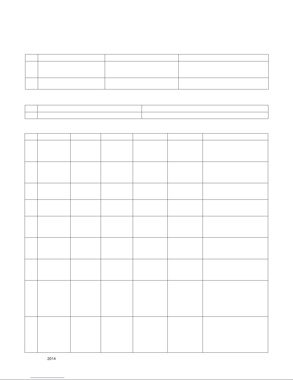
4. General Specification
No Item Specication Remark
1. Display Screen Device 32” wide Color Display Module Resolution: 1366*768
32” wide Color Display Module Resolution: 1920*1080
39” wide Color Display Module Resolution: 1920*1080
42” wide Color Display Module Resolution: 1920*1080
47” wide Color Display Module Resolution: 1920*1080
50” wide Color Display Module Resolution: 1920*1080
55” wide Color Display Module Resolution: 1920*1080
60” wide Color Display Module Resolution: 1920*1080
70” wide Color Display Module Resolution: 1920*1080
2. Aspect Ratio 16:9 All
3. LCD Module 32" TFT WUXGA LCD
32" TFT WXGA LCD
39" TFT WXGA LCD
42" TFT WUXGA LCD
47” TFT WUXGA LCD
50” TFT WUXGA LCD
55” TFT WUXGA LCD
60” TFT WUXGA LCD
70” TFT WUXGA LCD
4. Operating Environment TFT 1) Temp. : 0 ~ 40 deg
2) Humidity : 0 ~ 85%
LGE SPEC
5. Storage Environment TFT 1) Temp. : -20 ~ 60 deg
2) Humidity : 10 ~ 90%
6. Input Voltage AC100 ~ 240V, 50/60Hz
7. Power Consumption(Max) =
LCD(Module) + Backlight(LED)
FHD
T240Hz
Slim Direct
60”’ 72.16 W
LC600DUF-FGP1 [60LB720T-DA]
FHD
M120Hz
Direct
39” 45.74 W T390HVJ01.2 [39LB650T-DF]
42’’ TBD W LC420DUH-FGP2 [42LB6500-DF / 42LB650T-DF]
47’’ TBD W LC470DUH-FGP2 [47LB6500-DF / 47LB650T-DF]
50’’ 64.1 W LC500DUH-FGP2 [50LB6500-DF / 50LB650T-DF]
55’’ 62.5 W LC550DUH-FGP2 [55LB6500-DF / 55LB650T-DF]
60’’ TBD W LC600DUF-FGP2 [60LB6500-DF / 60LB650T-DF]
FHD
M120Hz
Direct M
70” 189.5 W HC700DUF-VHHD2[70LB720T-DA]
60” 71.16 W LC600DUF-FGP1[60LB720T-DA]
55” 68.2 W LC550DUH-PGF1 [55LB700T-DF/6700-DA]
47” 41.29 W LC470DUH-PGF1 [47LB700T-DF/6700-DA]
42” 38.4 W LC420DUH-PGF1 [42LB700T-DF/6700-DA]
FHD
T240Hz
Edge LED
49”’ 50.24 W FPR : LC490EUH-LGF1 [49LB870T-DA]

- 8 -
LGE Internal Use OnlyCopyright © LG Electronics. Inc. All rights reserved.
Only for training and service purposes
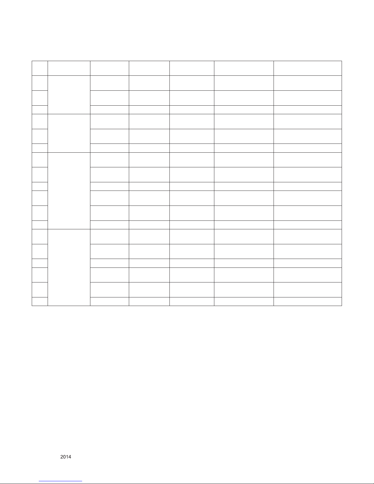
8. LCD Module Size Maker Inch (H) × (V) × (D)
LGD 42” 959.5 x 559.5 x 25.0 LC420DUH-FGP2
[42LB6500-DF / 42LB650T-DF]
944.4 x 542.7 x 25.0 LC420DUH-PGF1
[42LB700T-DF/6700-DA]
47” 1071 x.621.6x26.3 LC470DUH-FGP2
[47LB6500-DF / 47LB650T-DF]
1056.1 x 605.5 x 25.0 LC470DUH-PGF1
[47LB700T-DF/6700-DA]
49” 1086.3 X 622.0 X 9.9 LC490EUH-LGF1 [49LB870T-DA]
50” 1126.11 x 652.5 x 26.3 LC500DUH-FGP2
[50LB6500-DF / 50LB650T-DF]
55” 1241.19 x 717.94 x 26 LC550DUH-FGP2
[55LB6500-DF / 55LB650T-DF]
1226.0 x 701.1 x 25.0 LC550DUH-PGF1
[55LB700T-DF/6700-DA]
60” 1350.89x 780.54 x 28 LC600DUF-FGP1 [60LB720T-DA]
1346.8 x 774.4 x 29.9 LC600DUF-FGP2
[60LB6500-DF / 60LB650T-DF]
HeeSung 70” 1574.06 x 912.19 x30 HC700DUF-VHHD2[70LB720T-DA]
Pixel Pitch Maker Inch (H) × (V) × (D)
AUO 39’’ 444.75 x 444.75 T390HVJ01.2 [39LB650T-DF]
LGD 42’’ 541.5 x 541.5 LC420DUH-FGP2
[42LB6500-DF / 42LB650T-DF]
LC420DUH-PGF1
[42LB700T-DF/6700-DA]
47” 559.3 x 559.3 LC470DUH-FGP2
[47LB6500-DF / 47LB650T-DF]
LC470DUH-PGF1
[47LB700T-DF/6700-DA]
49” 570.75 x 570.75 LC490EUH-LGF1 [49LB870T-DA]
50” 630 x 630 LC500DUH-FGP2
[50LB6500-DF / 50LB650T-DF]
55” 686.1 x 686.1 LC550DUH-FGP2
[55LB6500-DF / 55LB650T-DF]
LC550DUH-PGF1
[55LB700T-DF/6700-DA]
60” 483.3 x 483.3 LC600DUF-FGP1 [60LB720T-DA]
TBD LC600DUF-FGP2
[60LB6500-DF / 60LB650T-DF]
HeeSung 70” 802 x 802 HC700DUF-VHHD2
[70LB720T-DA]
- 9 -
LGE Internal Use OnlyCopyright © LG Electronics. Inc. All rights reserved.
Only for training and service purposes
9. Back Light Maker Inch TYPE Module Name
LGD 42” Edge
47”
49” FPR : LC490EUH-LGF1 [49LB870T-DA]
50”
55”
55 Direct M LC550DUH-PGF1
[55LB700T-DF/6700-DA]
47” LC470DUH-PGF1
[47LB700T-DF/6700-DA]
42” LC420DUH-PGF1
[42LB700T-DF/6700-DA]
60” LC600DUF-FPG1 [ 60LB720T-DA]
70” HC700DUF-VHHD2[70LB720T-DA]
39’’ Direct L T390HVJ01.2 [39LB650T-DF]
42’’ LC420DUH-FGP2
[42LB6500-DF / 42LB650T-DF]
47 LC470DUH-FGP2
[47LB6500-DF / 47LB650T-DF]
50 LC500DUH-FGP2
[50LB6500-DF / 50LB650T-DF]
55 LC550DUH-FGP2
[55LB6500-DF / 55LB650T-DF]
60’’ LC600DUF-FGP2
[60LB6500-DF / 60LB650T-DF]
Display Colors 1.06 B (10-bit) Except FHD 60Hz models
16.7 M (8-bit) FHD/HD 60Hz models
AUO_T390HVJ01.2 [39LB6500]
Coating 3H(Hard coating), Anti-glare
- 10 -
LGE Internal Use OnlyCopyright © LG Electronics. Inc. All rights reserved.
Only for training and service purposes
5. External Input Support Format
5.1. Component input(Y, CB/PB, CR/PR)
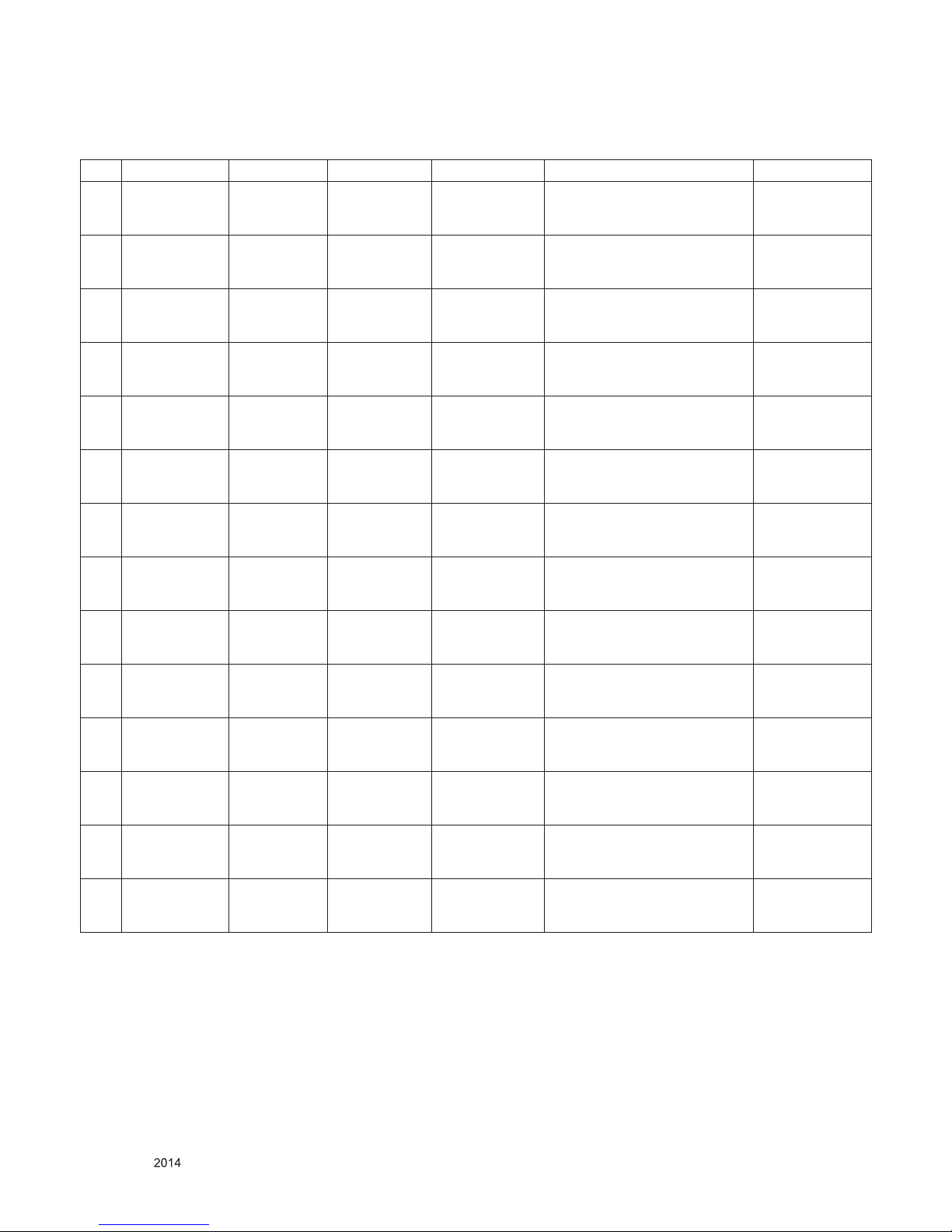
No Resolution H-freq(kHz) V-freq.(kHz) Pixel clock Proposed
1. 720*480 15.73 60 13.5135 SDTV ,DVD 480I
2. 720*480 15.73 59.94 13.5 SDTV ,DVD 480I
3. 720*480 31.50 60 27.027 SDTV 480P
4. 720*480 31.47 59.94 27.00 SDTV 480P
5. 720*576 15.625 50* 13.5 SDTV 576I
6. 720*576 31.25 50* 13.5 SDTV 576P
7. 1280*720 37.5 50* 74.25 HDTV 720P
8. 1280*720 45.00 60.00 74.25 HDTV 720P
9. 1280*720 44.96 59.94 74.176 HDTV 720P
10. 1929*1080 28.125 50* 74.25 HDTV 1080I
11. 1920*1080 33.75 60.00 74.25 HDTV 1080I
12. 1920*1080 33.72 59.94 74.176 HDTV 1080I
13. 1920*1080 56.25 50* 148.5 HDTV 1080P
14. 1920*1080 67.50 60 148.50 HDTV 1080P
15. 1920*1080 67.432 59.94 148.352 HDTV 1080P
16. 1920*1080 27.00 24.00 74.25 HDTV 1080P
17. 1920*1080 26.97 23.976 74.176 HDTV 1080P
18. 1920*1080 33.75 30.00 74.25 HDTV 1080P
19. 1920*1080 33.71 29.97 74.176 HDTV 1080P

- 11 -
LGE Internal Use OnlyCopyright © LG Electronics. Inc. All rights reserved.
Only for training and service purposes
5.2.2. PC mode
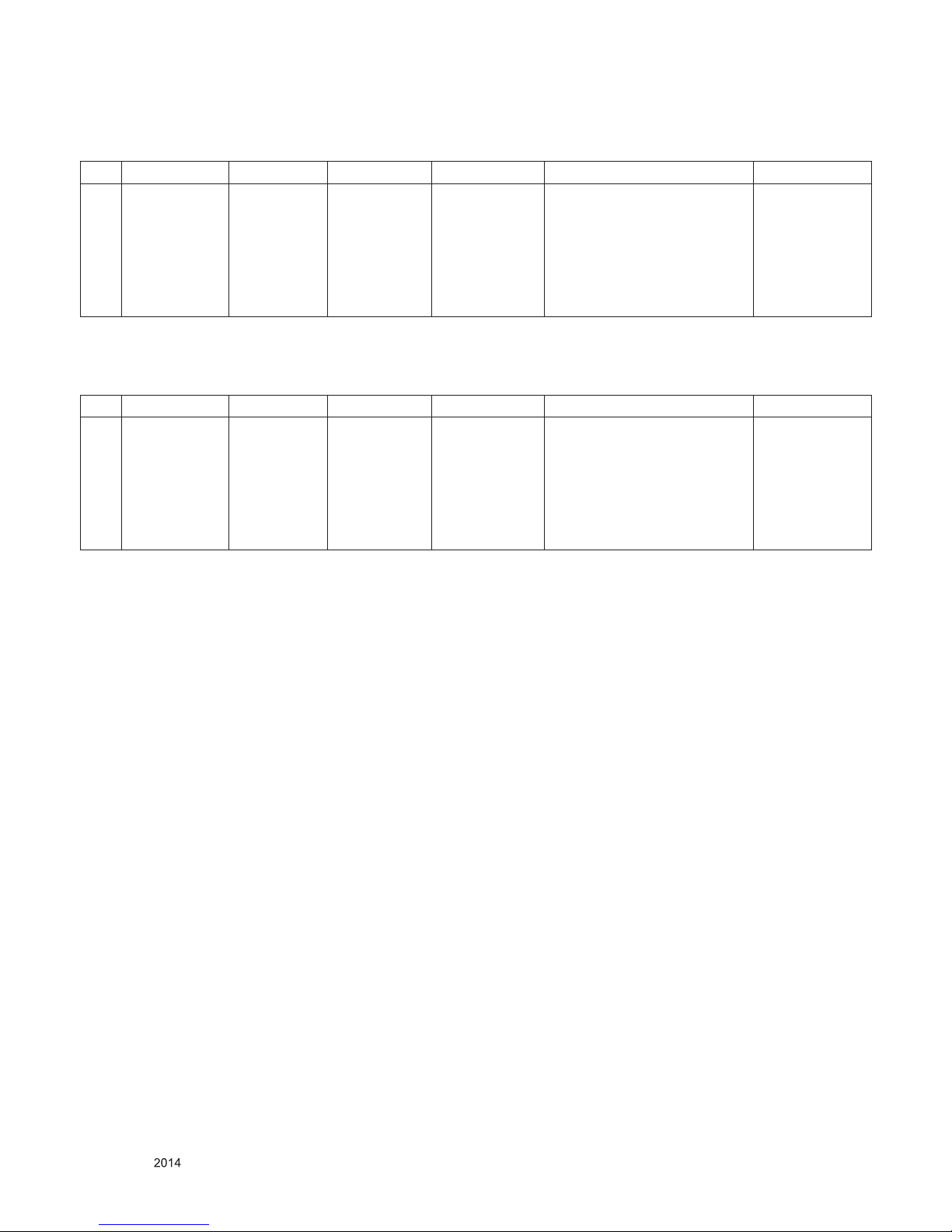
No. Resolution H-freq(kHz) V-freq.(kHz) Pixel clock Proposed Remarks
1 640*350 31.468 70.09 25.17 EGA
2 720*400 31.469 70.09 28.32 DOS
3 640*480 31.469 59.94 25.17 VESA(VGA)
4 800*600 37.879 60.31 40 VESA(SVGA)
5 1024*768 48.363 60.00 65 VESA(XGA)
6 1152*864 54.348 60.053 80.002 VESA(VGA)
7 1360*768 47.712 60.015 84.75 VESA(WXGA)
8 1280*1024 63.981 60.020 109.00 SXGA
Only FHD Model (Support to HDMI-PC)
9 1920*1080 67.5 60 158.40 WUXGA (Reduced Blanking) Only FHD Model
5.2. HDMI : EDID DATA : Refer to adjust specification
5.2.1. DTV mode
No Resolution H-freq(kHz) V-freq.(Hz)
Pixel
clock(MHz)
Proposed Remark
1 720*480 15.73 59.94 13.500 SDTV, DVD 480I(525I) Spec. out but display
2 15.75 60.00 13.514 SDTV, DVD 480I(525I)
3 720*576 15.625 50.00 13.500 SDTV, DVD 576I(625I) 50Hz
4 720*480 31.47 59.94 27 SDTV 480P
5 31.5 60.00 27.027 SDTV 480P
6 720*576 31.25 50.00 27 SDTV 576P
7 1280*720 44.96 59.94 74.176 HDTV 720P
8 45 60.00 74.25 HDTV 720P
9 37.5 50.00 74.25 HDTV 720P
10 1920*1080 28.125 50.00 74.25 HDTV 1080I
11 33.72 59.94 74.176 HDTV 1080I
12 33.75 60.00 74.25 HDTV 1080I
13 26.97 23.976 63.296 HDTV 1080P
14 27.00 24.000 63.36 HDTV 1080P
15 33.71 29.97 79.120 HDTV 1080P
16 33.75 30.00 79.20 HDTV 1080P
17 56.25 50.00 148.5 HDTV 1080P
18 67.432 59.94 148.350 HDTV 1080P
19 67.5 60.00 148.5 HDTV 1080P
- 12 -
LGE Internal Use OnlyCopyright © LG Electronics. Inc. All rights reserved.
Only for training and service purposes
5.3. 3D mode
5.3.1. RF Input (3D supported mode manually)
No Resolution Proposed 3D input proposed mode
1 HD 1080I
720P
2D to 3D
Side by Side(Half)
Top & Bottom
2 SD 576P
576I
2D to 3D
5.3.2. RF Input (3D supported mode automatically)
5.3.3. HDMI Input 1.3(3D supported mode manually)
No Resolution H-freq(kHz) V-freq.(Hz) Pixel clock(MHz) Proposed Remark
1 1280*720 45.00 60.00 74.25 HDTV 720P 2D to 3D
Side by Side(half),
Top & Bottom,
Single Frame Sequential
2 1280*720 37.500 50 74.25 HDTV 720P 2D to 3D
Side by Side(half),
Top & Bottom,
Single Frame Sequential
3 1920*1080 33.75 60.00 74.25 HDTV 1080I 2D to 3D
Side by Side(half),
Top & Bottom
4 1920*1080 28.125 50.00 74.25 HDTV 1080I 2D to 3D
Side by Side(half),
Top & Bottom
5 1920*1080 27.00 24.00 74.25 HDTV 1080P 2D to 3D
Side by Side(half),
Top & Bottom,
Checkerboard
6 1920*1080 28.12 25 74.25 HDTV 1080P 2D to 3D
Side by Side(half),
Top & Bottom,
Checkerboard
7 1920*1080 33.75 30.00 74.25 HDTV 1080P 2D to 3D
Side by Side(half),
Top & Bottom,
Checkerboard
8 1920*1080 56.25 50 148.5 HDTV 1080P 2D to 3D
Side by Side(half),
Top & Bottom,
Checkerboard,
Single Frame Sequential,
Row Interleaving,
Column Interleaving
9 1920*1080 67.50 60.00 148.5 HDTV 1080P 2D to 3D
Side by Side(half),
Top & Bottom,
Checkerboard,
Single Frame Sequential,
Row Interleaving,
Column Interleaving
No Signal 3D input proposed mode
1 Frame Compatible Side by Side(Half), Top & Bottom
- 13 -
LGE Internal Use OnlyCopyright © LG Electronics. Inc. All rights reserved.
Only for training and service purposes
5.3.4. HDMI Input 1.4b (3D supported mode automatically)
No Resolution H-freq(kHz) V-freq.(Hz) Pixel clock(MHz) 3D input proposed
mode
Proposed
1 640*480 31.469 / 31.5 59.94/ 60 25.175/25.2 Top-and-Bottom
Side-by-side(half)
Secondary(SDTV 480P)
Secondary(SDTV 480P)
2 62.938 / 63 59.94/ 60 50.35/50.4 Frame packing
Line alternative
Secondary(SDTV 480P)
(SDTV 480P)
3 31.469 / 31.5 59.94/ 60 50.35/50.4 Side-by-side(Full) (SDTV 480P)
4 720*480 31.25 50 27 Top-and-Bottom
Side-by-side(half)
Secondary(SDTV 480P)
Secondary(SDTV 480P)
5 62.5 50 54 Frame packing
Line alternative
Secondary(SDTV 480P)
(SDTV 480P)
6 31.25 50 54 Side-by-side(Full) (SDTV 480P)
7 720*576
(576p)
31.25 50 27 Top-and-Bottom
Side-by-side(half)
Secondary(SDTV 576P)
Secondary(SDTV 576P)
8 62.5 50 54 Frame packing
Line alternative
Secondary(SDTV 576P)
(SDTV 576P)
9 31.25 50 54 Side-by-side(Full) (SDTV 576P)
10 720 (1440)*576
(576i)
15.625 50 27 Top-and-Bottom
Side-by-side(half)
Secondary(SDTV 576I)
Secondary(SDTV 576I)
11 31.25 50 54 Frame packing
Field alternative
Secondary(SDTV 576I)
(SDTV 576I)
12 15.625 50 54 Side-by-side(Full) (SDTV 576I)
13 1280*720 37.5 50 74.25 Top-and-Bottom
Side-by-side(half)
Primary(HDTV 720P)
Primary(HDTV 720P)
14 75 50 148.5 Frame packing
Line alternative
Primary(HDTV 720P)
(HDTV 720P)
15 37.5 50 148.5 Side-by-side(Full) (HDTV 720P)
16 44.96 / 45 59.94 / 60 74.18/74.25 Top-and-Bottom
Side-by-side(half)
Primary(HDTV 720P)
Primary(HDTV 720P)
17 89.91 / 90 59.94 / 60 148.35/148.5 Frame packing
Line alternative
Primary(HDTV 720P)
(HDTV 720P)
18 44.96 / 45 59.94 / 60 148.35/148.5 Side-by-side(Full) (HDTV 720P)

- 14 -
LGE Internal Use OnlyCopyright © LG Electronics. Inc. All rights reserved.
Only for training and service purposes
No Resolution H-freq(kHz) V-freq.(Hz) Pixel clock(MHz) 3D input proposed
mode
Proposed
19 1920*1080 33.72 / 33.75 59.94 / 60 74.18/74.25 Top-and-Bottom
Side-by-side(half)
Secondary(HDTV 1080I)
Primary(HDTV 1080I)
20 67.432 / 67.5 59.94 / 60 148.35/148.5 Frame packing
Field alternative
Primary(HDTV 1080I)
(HDTV 1080I)
21 33.72 / 33.75 59.94 / 60 148.35/148.5 Side-by-side(Full) (HDTV 1080I)
22 28.125 50.00 74.25 Top-and-Bottom
Side-by-side(half)
Secondary(HDTV 1080I)
Primary(HDTV 1080I)
23 56.25 50.00 148.5 Frame packing
Field alternative
Primary(HDTV 1080I)
(HDTV 1080I)
24 28.125 50.00 148.5 Side-by-side(Full) (HDTV 1080I)
25 26.97 / 27 23.97 / 24 74.18/74.25 Top-and-Bottom
Side-by-side(half)
Primary(HDTV 1080P)
Primary(HDTV 1080P)
26 43.94 / 54 23.97 / 24 148.35/148.5 Frame packing
Line alternative
Primary(HDTV 1080P)
(HDTV 1080P)
27 26.97 / 27 23.97 / 24 148.35/148.5 Side-by-side(Full) (HDTV 1080P)
28 28.12 25 74.25 Top-and-Bottom
Side-by-side(half)
Secondary(HDTV 1080P)
Secondary(HDTV 1080P)
29 56.25 25 148.5 Frame packing
Line alternative
Secondary(HDTV 1080P)
(HDTV 1080P)
30 28.125 25 148.5 Side-by-side(Full) (HDTV 1080P)
31 33.716 / 33.75 29.976 / 30.00 74.18/74.25 Top-and-Bottom
Side-by-side(half)
Primary(HDTV 1080P)
Secondary(HDTV 1080P)
32 67.432 / 67.5 29.976 / 30.00 148.35/148.5 Frame packing
Line alternative
Primary(HDTV 1080P)
(HDTV 1080P)
33 33.716 / 33.75 29.976 / 30.00 148.35/148.5 Side-by-side(Full) (HDTV 1080P)
34 56.25 50 148.5 Top-and-Bottom
Side-by-side(half)
Primary(HDTV 1080P)
Secondary(HDTV 1080P)
35 67.43 / 67.5 59.94 / 60 148.35/148.50 Top-and-Bottom
Side-by-side(half)
Primary(HDTV 1080P)
Secondary(HDTV 1080P)
5.3.5. HDMI-PC 3D Input (3D supported mode manually)
No Resolution H-freq(kHz) V-freq.(Hz) Pixel clock(MHz) 3D input proposed mode Proposed
1 1024*768 48.36 60 65 2D to 3D,
Side by Side(half)
Top & Bottom
HDTV 768P
2 1360*768 47.71 60 85.5 2D to 3D,
Side by Side(half)
Top & Bottom
HDTV 768P
3 1920*1080 67.500 60 148.50 2D to 3D,
Side by Side(half)
Top & Bottom,
Checker Board,
Single Frame Sequential
Row Interleaving,
Column Interleaving
HDTV 1080P
4 Others - - - 2D to 3D 640*350
720*400
640*480
800*600
1152*864
- 15 -
LGE Internal Use OnlyCopyright © LG Electronics. Inc. All rights reserved.
Only for training and service purposes
5.3.6. Component 3D Input (3D supported mode manually)
No Resolution H-freq(kHz) V-freq.(Hz) Pixel clock(MHz) 3D input proposed mode Proposed
1 1280*720 37.5 50 74.25 2D to 3D,
Side by Side(half),
Top & Bottom
HDTV 720P
2 1280*720 45.00 60.00 74.25 2D to 3D,
Side by Side(half),
Top & Bottom
HDTV 720P
3 1280*720 44.96 59.94 74.176 2D to 3D,
Side by Side(half)
Top & Bottom
HDTV 720P
4 1920*1080 33.75 60.00 74.25 2D to 3D,
Side by Side(half)
Top & Bottom
HDTV 1080I
5 1920*1080 33.72 59.94 74.176 2D to 3D,
Side by Side(half)
Top & Bottom
HDTV 1080I
6 1920*1080 28.12 50 74.25 2D to 3D,
Side by Side(half)
Top & Bottom
HDTV 1080I
7 1920*1080 67.500 60 148.50 2D to 3D,
Side by Side(half)
Top & Bottom
HDTV 1080P
8 1920*1080 67.432 59.94 148.352 2D to 3D,
Side by Side(half)
Top & Bottom
HDTV 1080P
9 1920*1080 27.000 24.000 74.25 2D to 3D,
Side by Side(half)
Top & Bottom
HDTV 1080P
10 1920*1080 28.12 25 74.25 2D to 3D,
Side by Side(half)
Top & Bottom
HDTV 1080P
11 1920*1080 56.25 50 74.25 2D to 3D,
Side by Side(half)
Top & Bottom
HDTV 1080P
12 1920*1080 26.97 23.976 74.176 2D to 3D,
Side by Side(half)
Top & Bottom
HDTV 1080P
13 1920*1080 33.75 30.000 74.25 2D to 3D,
Side by Side(half)
Top & Bottom
HDTV 1080P
14 1920*1080 33.71 29.97 74.176 2D to 3D,
Side by Side(half)
Top & Bottom
HDTV 1080P
- 16 -
LGE Internal Use OnlyCopyright © LG Electronics. Inc. All rights reserved.
Only for training and service purposes
5.3.7. USB Input (3D) (3D supported mode manually)
No Resolution H-freq(kHz) V-freq.(Hz) Pixel clock(MHz) 3D input proposed mode Proposed
1 1920*1080 33.75 30 74.25 2D to 3D
Side by Side(Half)*,
Top & Bottom*,
Checkerboard*
Row Interleaving,
Column Interleaving
(Photo : side by Side(half),
Top & Bottom)
HDTV 1080P
5.2.8. DLNA Input (3D)
No Resolution H-freq(kHz) V-freq.(Hz) Pixel clock(MHz) 3D input proposed mode Proposed
1 1920*1080 33.75 30 74.25 2D to 3D
Side by Side(Half)*,
Top & Bottom*,
Checkerboard*
Row Interleaving,
Column Interleaving
(Photo : side by Side(half), Top
& Bottom)
HDTV 1080P
- 17 -
LGE Internal Use OnlyCopyright © LG Electronics. Inc. All rights reserved.
Only for training and service purposes
ADJUSTMENT INSTRUCTION
1. Application Range
This specification sheet is applied all of the LT42B LED TV
models, which produced in manufacture department or similar
LG TV factory
2. Notice
(1) Because this is not a hot chassis, it is not necessary to use
an isolation transformer. However, the use of isolation
transformer will help protect test instrument.
(2) Adjustment must be done in the correct order. But it is
flexible when its factory local problem occurs.
(3) The adjustment must be performed in the circumstance of
25 ±5ºC of temperature and 65±10% of relative humidity if
there is no specific designation.
(4) The input voltage of the receiver must keep 100~220V,
50/60Hz.
(5) Before adjustment, execute Heat-Run for 5 minutes.
▪ After Receive 100% Full white pattern (06CH) then process
Heat-run
(or “8. Test pattern” condition of Ez-Adjust status)
▪ How to make set white pattern
1) Press Power ON button of Service Remocon
2) Pr ess ADJ button of Service remocon. Select “8. Test
pattern” and, after select “White” using navigation button,
and then you can see 100% Full White pattern.
* In this status you can maintain Heat-Run useless any pattern
generator
* Notice : if you mai nt ain one pictu re ov er 20 minutes
(Especially sharp distinction black with white pattern
-13Ch, or Cross hatch pattern – 09Ch) then it can
appear image stick near black level.
3. Adjustment items
3.1. PCB Assembly Adjustment
▪ MAC Address / ESN / Widevine / HDCP1.4 / HDCP 2.0
Download
▪ EDID (The Extended Display Identification Data)/DDC
(Display Data Channel) download
* If it is necessary, it can adjustment at Manufacture Line
You can see set adjustment status at “1. ADJUST CHECK”
of the “In-start menu”
3.2. Set Assembly Adjustment
▪ Color Temperature (White Balance) Adjustment
▪ Using RS-232C
▪ PING Test
▪ Selection Factory output option
4. PCB Assembly Adjustment
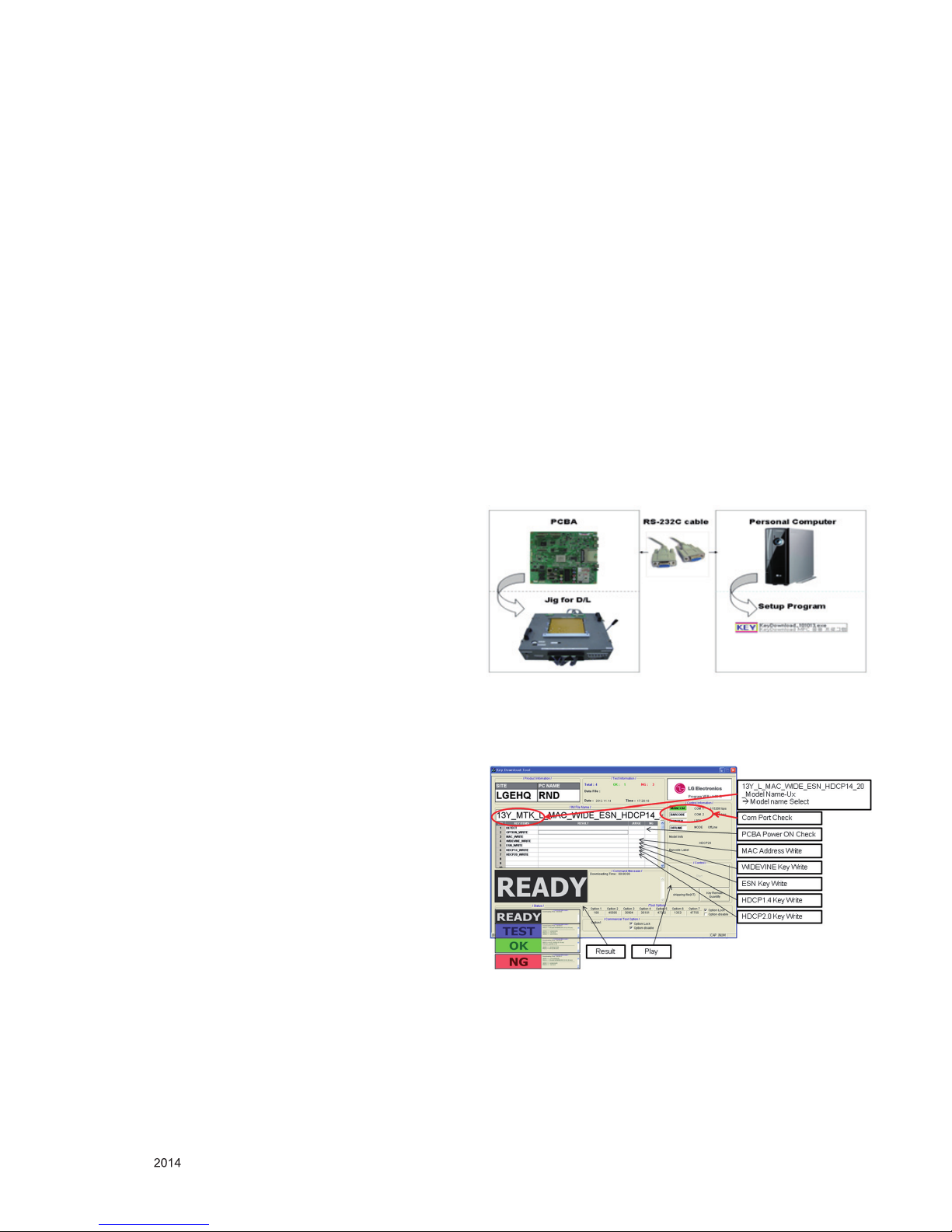
4.1. MAC Address, ESN Key and Widevine
Key download
4.1.1. Equipment & Condition
1) Play file: keydownload.exe
4.1.2. Communication Port connection
1) Key Write: Com 1,2,3,4 and 115200 (Baudrate)
2) Barcode: Com 1,2,3,4 and 9600 (Baudrate)
4.1.3. Download process
1) Select the download items.
2) Mode check: Online Only
3) Check the test process
- DETECT -> MAC_WRITE -> ESN_WRITE -> WIDEVINE_
WRITE
4) Play : START
5) Check of result: Ready, Test, OK or NG
4.1.4. Communication Port connection
1) Connect: PCBA Jig -> RS-232C Port == PC -> RS-232C
Port
4.1.5. Download
1) 14Y LCD TV+MAC+Widevine+ESN Key+ HDCP1.4 and
HDCP2.0
4.1.6. Inspection
- In INSTART menu, check these keys.

- 18 -
LGE Internal Use OnlyCopyright © LG Electronics. Inc. All rights reserved.
Only for training and service purposes
4.2. LAN PORT INSPECTION(PING TEST)
4.2.1. Equipment setting
1) Play the LAN Port Test PROGRAM.
2) Input IP set up for an inspection to Test
Program.
*IP Number : 12.12.2.2.
4.2.2. LAN PORT inspection (PING TEST)
1) Play the LAN Port Test Program.
2) connect each other LAN Port Jack.
3) Play Test (F9) button and confirm OK Message.
4) remove LAN CABLE
4.3. ADC Adjust => No need at Assembly
line because of OPT type
* OTP mode
Automatic ADC Calibration. (Internal ADC Calibration) On the
manufacture line, OTP is used
for ADC Calibration automatically.
* External mode
Manual ADC Calibration. When OTP mode is failed, ADC
calibration should be “OK” by
using External mode.
- If you want re-adjust for ADC.
■ Enter Service Mode by pushing “ADJ” key,
■ Enter Internal ADC mode by pushing “►” key at “9. ADC
Calibration”
■
Adjustment protocol
Order Command Set response
(1) Inter the Adjustment mode aa 00 00 a 00 OK00x
(2) Change the Source xb 00 40 b 00 OK40x (Adjust 480i Comp1 )
(Adjust 1080p Comp1)
(3) Start Adjustment ad 00 10
(4) Return the Response OKx ( Success condition )
NGx ( Failed condition )
(5) Read Adjustment data ( main)
ad 00 20
( main )
ad 00 30
(main : component1 480i)
000000000000000000000000007c007b006dx
(main : component1 1080p)
000000070000000000000000007c0083
0077x
(6) Conrm Adjustment ad 00 99 NG 03 00x (Failed condition)
NG 03 01x (Failed condition)
NG 03 02x (Failed condition)
OK 03 03x (Success condition)
(7) End of Adjustment ad 00 90 d 00 OK90x
- 19 -
LGE Internal Use OnlyCopyright © LG Electronics. Inc. All rights reserved.
Only for training and service purposes
5. Factory Adjustment
5.1. EDID (The Extended Display Identification
Data)/DDC (Display Data Channel) Download
● Summary
▪ It is established in VESA, for communication between PC
and Monitor without order from user for building user
condition. It helps to make easily use realize “Plug and Play”
function. For EDID data write, we use DDC2B protocol.
● Auto Download (No need Writing EDID data in Assembly line)
▪ After Set Tool Option, then TV turn off and on finish auto
download
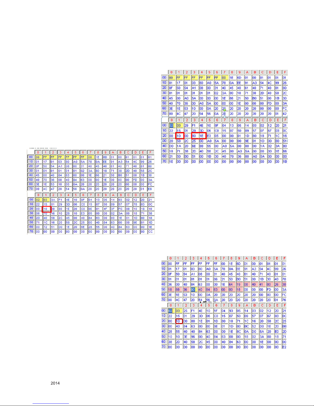
* EDID data for 3DTV (LB65/67/72/87 Serise) (Model name =
LG TV ) .
*Rev. 15xxx to confirm that, Rev. up subject to change
- HDMI EDID table
- HDMI-1 EDID table (0XE8, 0xCC)
A. If support 8bit (not support Deep color)
(1) HDMI 1 Check sum : 0xE8, 0XCC (CEA Block 0x21 :10)
(2) HDMI 2 Check sum : 0x E8, 0XBC (CEA Block 0x21 :20)
(3) HDMI 3 Check sum : 0x E8, 0XAC (CEA Block 0x21 :30)
B. If support 10bit (support Deep color)
(1) HDMI 1 Check sum : 0xE8, 0X85 (CEA Block 0x21 :10)
(2) HDMI 2 Check sum : 0x E8, 0X75 (CEA Block 0x21 :20)
(3) HDMI 3 Check sum : 0x E8, 0X65 (CEA Block 0x21 :30)
* EDID data for Non-3DTV (FHD) (Model name = LG TV )
*Rev. 24xxx to confirm that, Rev. up subject to change
- HDMI EDID table
- HDMI-1 EDID table (0x42, 0X1B)
A. If the LVDS supports 8bit (not support Deep color) , CEA
Block 0x23 :80, 0x24 : 1E)
(1) HDMI 1 Check sum : 0x42, 0X1B (CEA Block 0x21 :10)
(2) HDMI 2 Check sum : 0x42, 0X0B (CEA Block 0x21 :20)
(3) HDMI 3 Check sum : 0x42, 0XFB (CEA Block 0x21 :30)
B. If the LVDS supports 10bit (support Deep color) , CEA Block
0x23 :B8, 0x24 : 2D)
(1) HDMI 1 Check sum : 0x42, 0XD4 (CEA Block 0x21 :10)
(2) HDMI 2 Check sum : 0x42, 0XC4 (CEA Block 0x21 :20)
(3) HDMI 3 Check sum : 0x42, 0XB4 (CEA Block 0x21 :30
* EDID data for Non-3DTV (HD) (Model name = LG TV)
*Rev. 24xxx to confirm that, Rev. up subject to change
- HDMI EDID table
- HDMI-1 EDID table (0X76, 0XE2)
(1) HDMI 1 Check sum : 0X76, 0XE2 (CEA Block 0x21 :10)
(2) HDMI 2 Check sum : 0X76, 0XD2 (CEA Block 0x21 :20)
(3) HDMI 3 Check sum : 0X76, 0XC2 (CEA Block 0x21 :30)
- 20 -
LGE Internal Use OnlyCopyright © LG Electronics. Inc. All rights reserved.
Only for training and service purposes
5.2. Adjustment White balance
● W/B Equipment condition
CA210 : CH 14, Test signal : Inner pattern (80IRE) – LED
Module
CH18 , Test signal : Inner pattern (80IRE) – ALEF
Module
● Above 5 minutes H/run in the inner pattern. (“power on” key of
adjust remote control)
※ The spec of color temperature and coordinate.
All
Cool (C50) 13,000k K
X=0.271
(±0.002)
Y=0.270
(±0.002)
<Test signal>
- Inner pattern
for W/B adjust
- External white
pattern (80IRE,
204gray)
Medium (0) 9,300k K
X=0.286
(±0.002)
Y=0.289
(±0.002)
Warm (W50) 6,500k K
X=0.313
(±0.002)
Y=0.329
(±0.002)
※ Normal line(LGD Module (LB5xxx, LB6xxx, LB7xxx, LB8xxx))
- Except Winter Season ( Jan. , Feb. ) and Global table
H/R Time(Min)
Cool Medium Warm
x y x x y x
271 270 286 289 313 329
1 0-2 282 289 297 308 324 348
2 3-5 281 287 296 306 323 346
3 6-9 279 284 294 303 321 343
4 10-19 277 280 292 299 319 339
5 20-35 275 277 290 296 317 336
6 36-49 274 274 289 293 316 333
7 50-79 273 272 288 291 315 331
8 80-119 272 271 287 290 314 330
9 Over 120 271 270 286 289 313 329
※ AUO, INX, Sharp, CSOT, BOE Model (in case, Cool spec =
13000K)
cool med warm
x y x y x y
spec 271 270 286 289 313 329
target 278 280 293 299 320 339
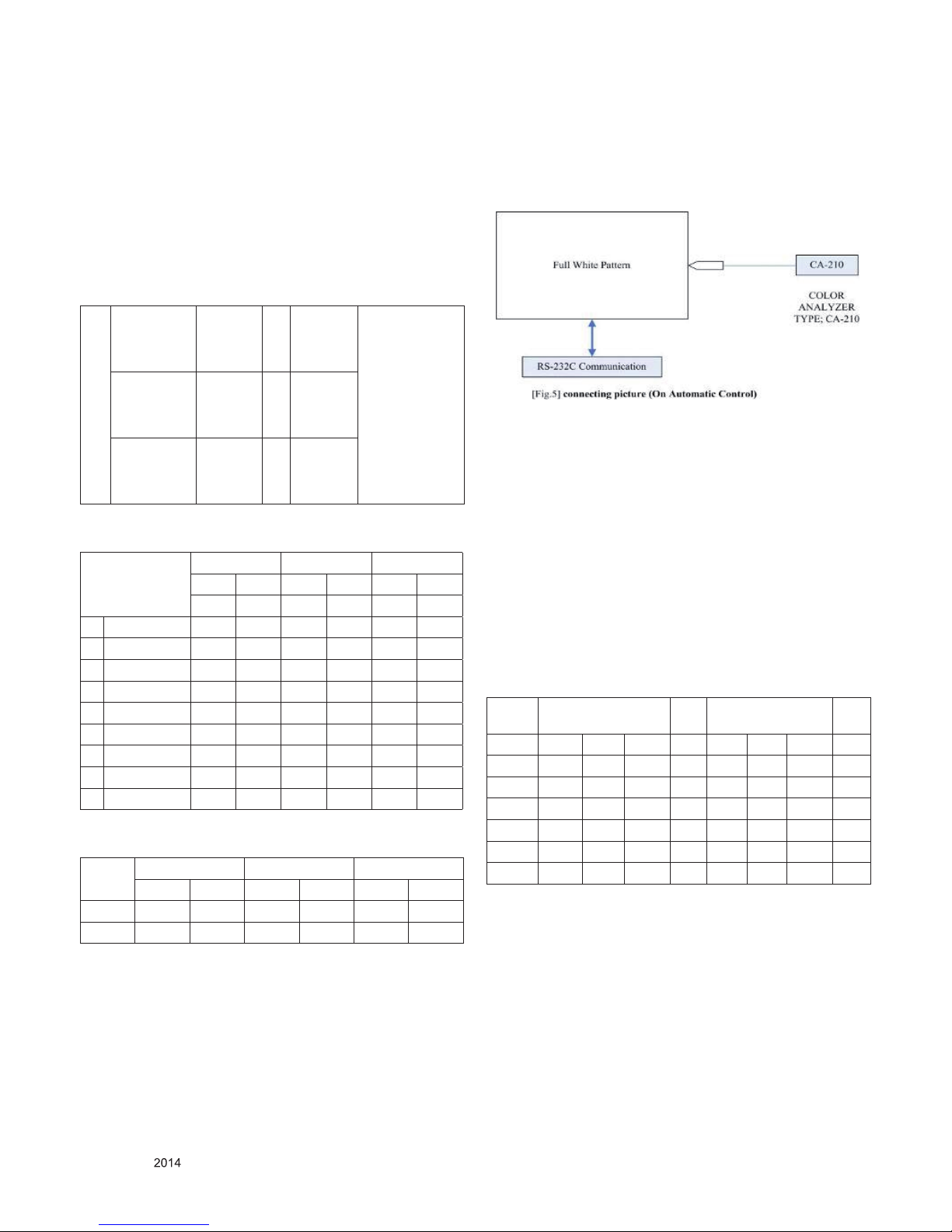
※ Connecting picture of the measuring instrument (On Automatic
control)
Inside PATTERN is used when W/B is controlled. Connect to
auto controller or push Adjustment R/C POWER-ON -> Enter
the mode of White-Balance, the pattern will come out
● Auto-control interface and directions
(1) Adjust in the place where the influx of light like floodlight
around is blocked. (Illumination is less than 10ux).
(2) Adhere closely the Color Analyzer ( CA210 ) to the module
less than 10cm distance, keep it with the surface of the
Module and Color Analyzer’s Prove vertically.(80~100°).
(3) Aging time
- After aging start, keep the power on (no suspension of power
supply) and heat-run over 5 minutes.
- Using ‘no signal’ or ‘full white pattern’ or the others, check the
back light on.
● Auto adjustment Map(RS-232C)
RS-232C COMMAND
[ CMD ID DATA ]
Wb 00 00 White Balance Start
Wb 00 ff White Balance End
RS-232C COMMAND
[CMD ID DATA]
MIN CENTER
(DEFAULT)
MAX
Cool Mid Warm 00 Cool Mid Warm
R Gain Jg ja jd 00 172 192 192 192
G Gain Jh jb je 00 172 192 192 192
B Gain Ji jc jf 192 192 172 192
R Gain 64 64 64 128
G Gain 64 64 64 128
B Gain 64 64 64 128
- 21 -
LGE Internal Use OnlyCopyright © LG Electronics. Inc. All rights reserved.
Only for training and service purposes
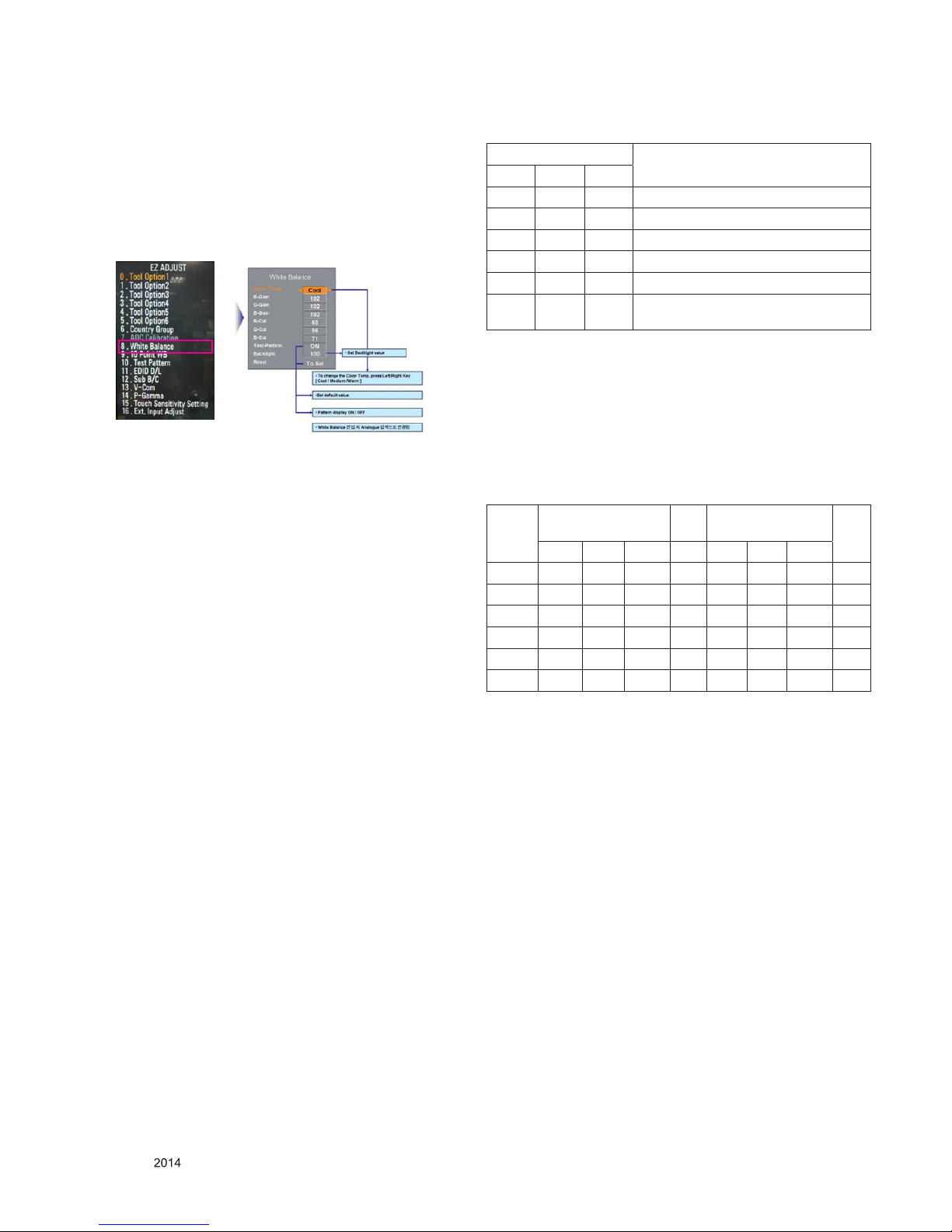
● Manual W/B process using adjusts Remote control.(TBD)
- Co lor analyzer(CA100+, CA210) should be used in the
calibrated ch by CS-1000
- Operate the zero-calibration of the CA100+ or CA-210, then
stick sensor to the module when adjusting.
- After enter Service Mode by pushing “ADJ” key,
- Enter White Balance by pushing “►” key at “8. White
Balance”
● For manual adjustment, it is also possible by the following
sequence
(1) Set TV in Adj. mode using “P-ONLY” key on remote controller
and then operate heat run longer than 15 minutes.
(I f not executed this step, the condition for W/B may be
different.)
(2) Push “Exit” key.
(3) Enter White Balance mode by pushing the ADJ key and select
“8. White Balance”. When KEY (►) is pressed, 206 Gray
internal pattern will be displayed.
(4) Zero Calibrate the probe of Color Analyzer, then place it on
the center of LCD module within 10cm of the surface
(5) Select each items (Red/Green/Blue Gain) using ▲/▼(CH +/-)
key on R/C..
(6) Adjust R/ G/ B Gain using ◄/►(VOL +/-) key on R/C.
(7) Adjust three modes all (Cool / Medium / Warm) -Fix the one of
R/G/B gain and change the others
(8) When adjustment is completed, exit adjustment mode using
EXIT key on R/C.
※ CASE Cool
- First adjust the coordinate far away from the target value(x, y).
(1) x, y > target
(i) Decrease the R, G.
(2) x, y < target
(i) First decrease the B gain,
(ii) Decrease the one of the others.
(3) x > target , y < target
(i) First decrease B, so make y a little more than the target.
(ii) Adjust x value by decreasing the R
(4) x < target , y > target
(i) First decrease B, so make x a little more than the target.
(ii) Adjust x value by decreasing the G
※ After You finish all adjustments, Press “In-start” button and
compare Tool option and Area option value with its BOM, if it is
correctly same then unplug the AC cable.
If it is not same, then correct it same with BOM and unplug AC
cable. For correct it to the model’s module from factory JIG
model.
※ Push The “I N STOP KEY” after completing the functi on
inspection.
● RS-232C Command (Commonly apply)
RS-232C COMMAND
Explanation
CMD DATA ID
wb 00 00 White Balance adjustment start
Wb 00 10
Start of adjust gain (Inner white pattern)
wb 00 1f End of gain adjust
wb 00 20
Start of offset adjust(Inner white pattern)
wb 00 2f End of offset adjust
wb 00 ff End of White Balance adjust
(Inner pattern disappeared)
▪ “wb 00 00”: Start Auto-adjustment of white balance.
▪ “wb 00 10”: Start Gain Adjustment (Inner pattern)
▪ “jb 00 c0” :
▪ …
▪ “wb 00 1f”: End of Adjustment
* If it needs, offset adjustment (wb 00 20-start, wb 00 2f-end)
▪ “wb 00 ff”: End of white balance adjustment (inner pattern
disappear)
※ Notice) Adjustment Mapping information
RS-232C COMMAND
[CMD ID DATA]
MIN CENTER
(DEFAULT)
MAX
Cool Mid Warm 00 Cool Mid Warm
R Gain Jg ja jd 00 172 192 192 192
G Gain Jh jb je 00 172 192 192 192
B Gain Ji jc jf 192 192 172 192
R Gain 64 64 64 128
G Gain 64 64 64 128
B Gain 64 64 64 128
5.3. Magic Motion remote controller Check
(Only LB67/LB69/LB772/LB87)
5.3.1 Test equipment
- RF-remote controller for check, IR-KEY-CODE remote
controller.
- Check AA battery before test. A recommendation is that a
tester change battery every lots.
5.3.2. Test
(1) Make pairing with TV set by pressing “Mute (START) key”
on RCU.
(2) Check a cursor on screen by pressing ‘ENTER” or “OK”
key of RCU
(3) Stop paring with TV set by pressing “VOL+ (STOP) key.
- 22 -
LGE Internal Use OnlyCopyright © LG Electronics. Inc. All rights reserved.
Only for training and service purposes
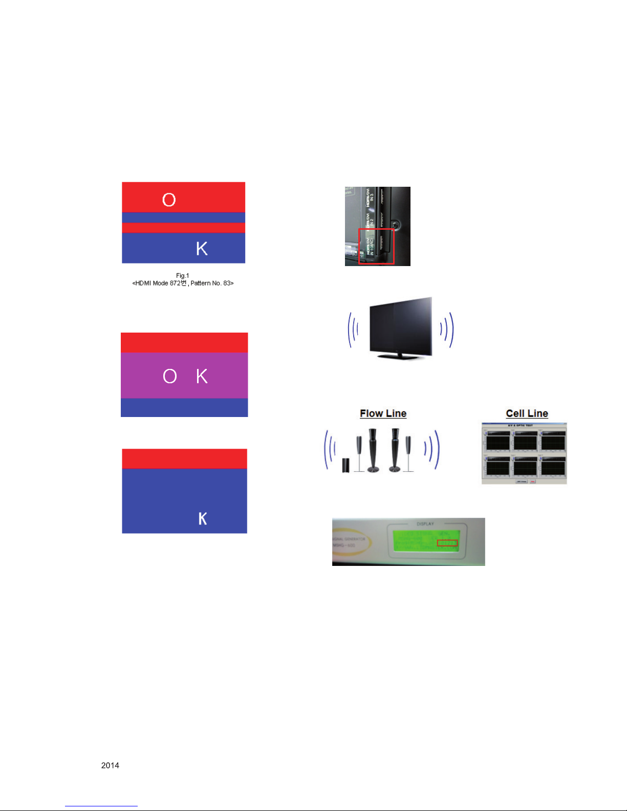
5.4. 3D pattern test
5.4.1. Test equipment
(1) Pattern Generator MSHG-600 or MSPG-6100 (HDMI 1.4
support)
(2) Pattern: HDMI mode (model No. 872, pattern No. 83)
5.4.2. Test method
(1) Input 3D test signal as Fig.1.
(2) Press ‘OK” key as a 3D input OSD is shown.
(3) Check pattern as Fig2 without 3D glasses. (3D mode
without 3D glasses)
Fig.2
<OK in 3D mode without 3D glasses>
Fig.3
<NG in 3D mode without 3D glasses>
5.5. HDMI ARC Function Inspection
5.5.1. Test equipment
- Optic Receiver Speaker
- MSHG-600 (SW: 1220 ↑)
- HDMI Cable (for 1.4 version)
5.5.2. Test method
(1) Insert the HDMI Cable to the HDMI ARC port from the
master equipment (HDMI1)
(2) Check the sound from the TV Set
(3) Check the Sound from the Speaker or using AV & Optic
TEST program (It’s connected to MSHG-600)
* Remark: Inspect in Power Only Mode and check SW version
in a master equipment
5.6. Selection of Country option
Selection of country option is allowed only North American
model (Not allowed Korean model). It is selection of Country
about Rating and Time Zone.
▪ Models: All models which use LJ22E Chassis (See the first
page.)
▪ Press “In-Start” button of Service Remocon, then enter the
“Option” Menu with “PIP CH-“ Button
▪ Select one of these three (USA, CANADA, MEXICO) defends
on its market using “Vol. +/-“button.
- 23 -
LGE Internal Use OnlyCopyright © LG Electronics. Inc. All rights reserved.
Only for training and service purposes
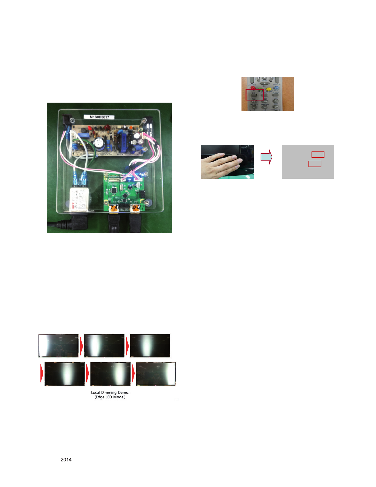
5.7. MHL Test
Step 1) Turn on TV
Step 2) Select HDMI4 mode using input Menu.
Step 3) Set MHL Zig(M1S0D3617) using MHL input, output
and power code.
Step 4) Connect HDMI cable between MHL Zig and HDMI4
port.
Step 5) Check LED light of Zig and Module of Set
Result) If, The LED light is green and The Module shows
normal stream -> OK
Else -> NG
※ Caution : Don’t push The INSTOP KEY after completing the
function inspection.
5.8. Local Dimming Function Check
Step 1) Turn on TV
Step 2) Press “TILT” key on the Adj. R/C
Step 3) At the Local Dimming mode, module Edge Backlight
moving left to right. Back light of IOP module moving
Step 4) confirm the Local Dimming mode.
Step 5) Press “exit” key.
5.9. Intelligent Sensor Inspection
Step 1) Turn on the TV set.
Step 2) Press “ EY E” button o n t he Adjust me nt remote
controller.
Step 3) Block the Intelligent Sensor module on the front C/A
about 6 seconds. When the “Sensor Data” is lower
than 20, you can see the “OK” message
=> If it doesn’t show “OK” message, the Sensor Module is
defected one. You have to replace that with a good one.
Step 4) After check the “OK” message come out, take out your
hand from the Sensor module
=> Check “Sensor Data” value change from “0” to “300” or
not. If it doesn’t change the value, the sensor is also
defected one. You have to replace it.
※ Caution : Don’t push The INSTOP KEY after completing the
function inspection
6. GND and HI-POT Testing
6.1. GND & HI-POT auto-check preparation
Check the connection between set and
power cord
(1) Check the POWER CABLE and SIGNAL CABE insertion
condition
6.2. GND & HI-POT auto-check
(1) Pallet moves in the station. (POWER CORD / AV CORD is
tightly inserted)
(2) Connect the AV JACK Tester
(3) Controller (GWS103-4) on.
(4) GND Test (Auto)
- If Test is failed, Buzzer operates.
- If Test is passed, execute next process (Hi-pot test).
(Remove A/V CORD from A/V JACK BOX)
(5) HI-POT test (Auto)
- If Test is failed, Buzzer operates.
- If Test is passed, GOOD Lamp on and move to next process
automatically
6.3. Check Point
(1) Test voltage
3 Poles : GND: 1.5KV/min at 100mA / SIGNAL: 3KV/min at
100mA
(2) TEST time: 1 second
(3) TEST POINT
3 Poles : GND Test = POWER CORD GND and SIGNAL
CABLE GND.
Hi-pot Test = POWER CORD GND and LIVE & NEUTRAL.
(4) LEAKAGE CURRENT: At 0.5mArms
Green Eye-Check
Sensor Data : 492
BackLight : 100
OK
- 24 -
LGE Internal Use OnlyCopyright © LG Electronics. Inc. All rights reserved.
Only for training and service purposes
7. Default Service option
7.1. ADC-Set
▪ R-Gain adjustment Value (default 128)
▪ G-Gain adjustment Value (default 128)
▪ B-Gain adjustment Value (default 128)
▪ R-Offset adjustment Value (default 128)
▪ G-Offset adjustment Value (default 128)
▪ B-Offset adjustment Value (default 128)
7.2. White balance. Value
CENTER (DEFAULT)
C50 0 W50
R Gain 192 192 192
G Gain 192 192 192
B Gain 192 192 192
R Cut 64 64 64
G Cut 64 64 64
B Cut 64 64 64
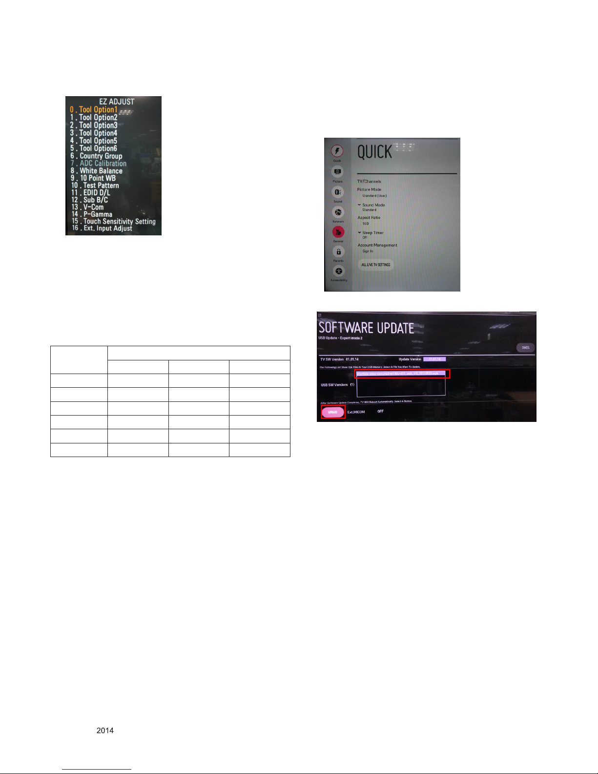
8. USB DOWNLOAD (*.epk file download)
(1) Put the USB Stick to the USB socket
(2) Press Menu key, and move General
*before 10.2 Step. Set USB Expert Mode : Enabled
IN START > System 3 > USB Expert Mode
(3) Press “number key 7” Press 7 times
(4) Select download file (epk file)
(5) After download is finished, remove the USB stick. ( it will be
auto-reboot )
(6) Press “IN-START” key of ADJ remote control, check the
S/W version.
- 25 -
LGE Internal Use OnlyCopyright © LG Electronics. Inc. All rights reserved.
Only for training and service purposes
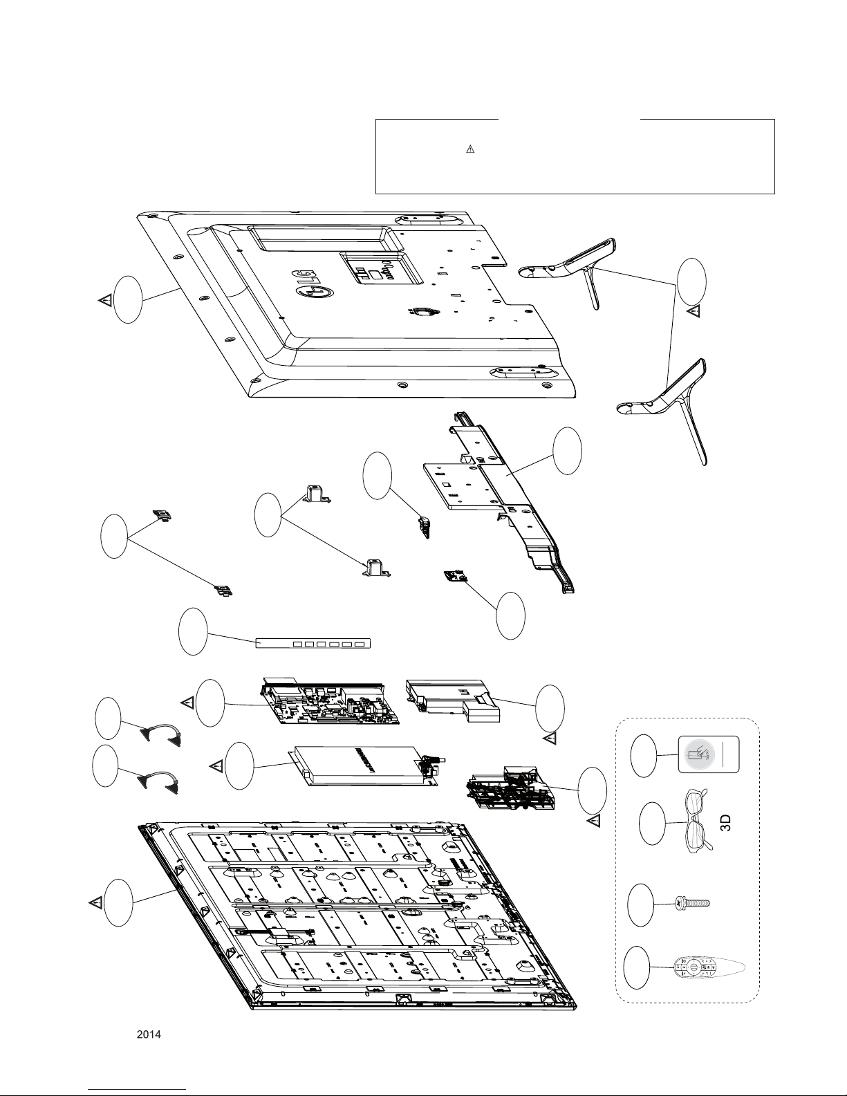
EXPLODED VIEW
Many electrical and mechanical parts in this chassis have special safety-related characteristics. These
parts are identified by in the Schematic Diagram and EXPLODED VIEW.
It is essenti al that these special safet y parts shoul d be replac ed with the same compo nents as
recommended in this manual to prevent X-RADIATION, Shock, Fire, or other Hazards.
Do not modify the original design without permission of manufacturer.
IMPORTANT SAFETY NOTICE
410
420
LV1
LV2
200
521
540
530
400
121
120
500
560
401
900
A10
A22
AG1
Set + Stand
AT1
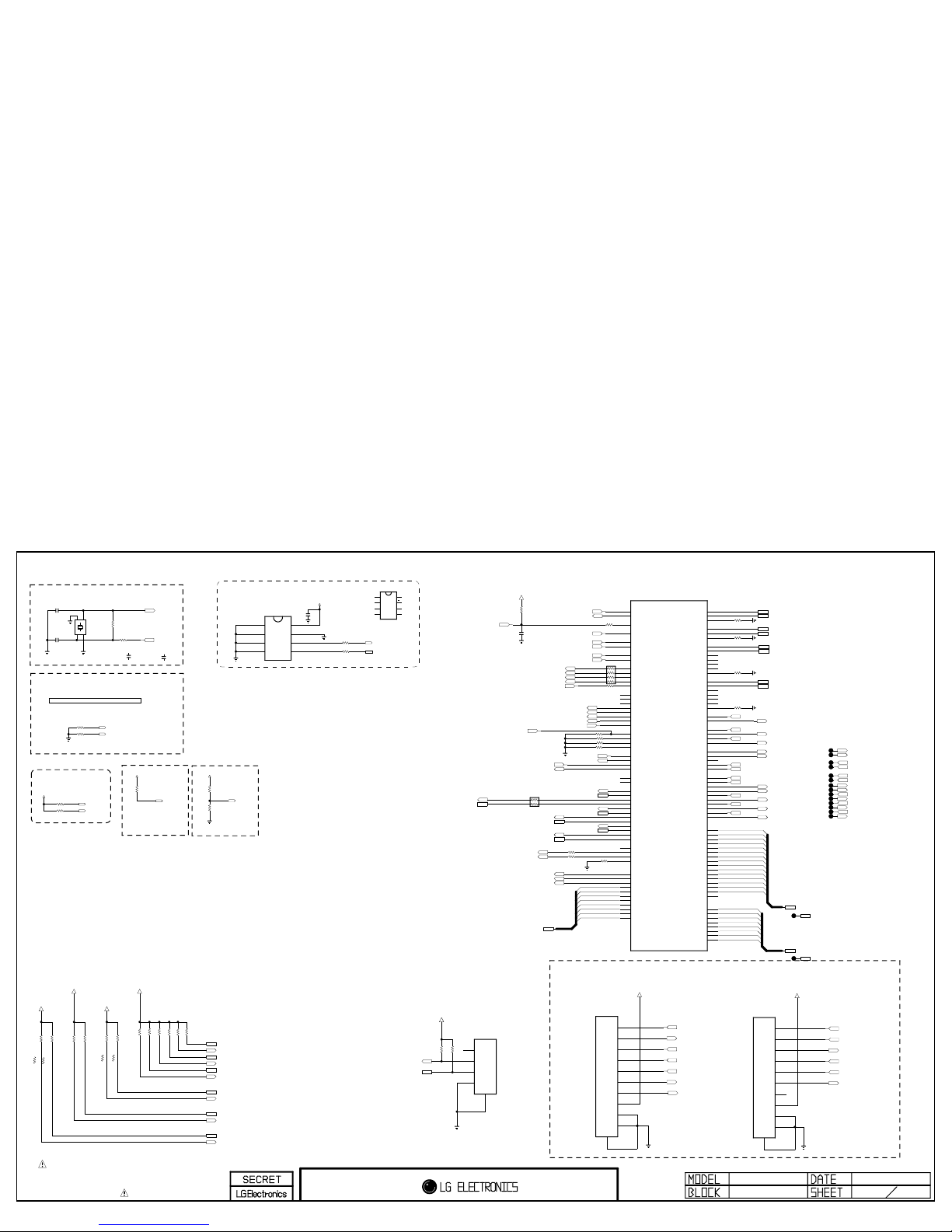
THE SYMBOL MARK OF THIS SCHEMETIC DIAGRAM INCORPORATES
SPECIAL FEATURES IMPORTANT FOR PROTECTION FROM X-RADIATION.
FIRE AND ELECTRICAL SHOCK HAZARDS, WHEN SERVICING IF IS
ESSENTIAL THAT ONLY MANUFACTURES SPECIFIED PARTS BE USED FOR
THE CRITICAL COMPONENTS IN THE SYMBOL MARK OF THE SCHEMETIC.
M14-Peripheral
EB_ADDR[4]
EMMC_DATA[0]
EB_ADDR[1]
EB_DATA[2]
EB_ADDR[3]
EMMC_DATA[2]
EB_ADDR[10]
EB_DATA[0]
EMMC_DATA[7]
EMMC_DATA[4]
EB_ADDR[13]
EB_ADDR[6]
EMMC_DATA[3]
EB_ADDR[0]
EB_ADDR[2]
EB_DATA[3]
EMMC_DATA[1]
EB_ADDR[8]
EMMC_DATA[6]
EB_ADDR[5]
EB_DATA[6]
EB_DATA[4]
EB_ADDR[9]
EB_ADDR[7]
EB_DATA[7]
EB_DATA[5]
EB_ADDR[12]
EB_ADDR[14]
EB_DATA[1]
EMMC_DATA[5]
EB_ADDR[11]
OPM1
CAM_INPACK_N
C101-*1
6.8pF
50V
LOADCAP_DVB_PCB
IRB_SPI_MISO/TDI1
C107
0.1uF
16V
R159
3.3K
TP111
I2C_SCL4
TRST_N1
USB_DP3
R101 3.3K
OPT
R156
1.2K
KR_PIP_NOT
TDI0
USB_DM1
SOC_RESET
USB_DP1
I2C_SCL2
LED_SDA
EB_ADDR[0-14]
/PCM_CE1
C102-*1
6.8pF
50V
LOADCAP_DVB_PCB
CAM_IREQ_N
PLLSET1
XTAL_IN
XTAL_IN
R104 3.3K
OPT
TRST_N1
R162
3.3K
OPM0
LED_SCL
R155-*1
3.3K
KR_PIP
I2C_SCL5
R108
33
I2C_SDA6
USB_CTL2
USB_CTL3
I2C_SDA2
EB_WE_N
R158
3.3K
R163
10K
OPT
EB_BE_N1
R182 10K
OPT
R161
3.3K
I2C_SCL4
R105
3.3K
OPT
TP113
IRB_SPI_MISO/TDI1
I2C_SDA1
IRB_SPI_MOSI/TDO1
XTAL_OUT
USB_CTL1
C104
0.1uF
16V
I2C_SDA6
I2C_SDA5
+3.3V_NORMAL
I2C_SDA5
R149
3.3K
TP116
EB_WE_N
I2C_SDA_MICOM_SOC
P102
12507WS-04L
OPT
1
2
3
4
5
I2C_SCL5
R183 10K
I2C_SDA1
PCM_RESET
INSTANT_BOOT
R148-*1
1.5K
KR_PIP
SOC_RESET
USB_DP2
EB_BE_N1
R102 3.3K
OPT
P104
12505WS-10A00
OPT
1
2
3
4
5
6
7
8
9
10
11
PLLSET0
/PCM_CE2
CAM_WAIT_N
PCM_5V_CTL
PLLSET0
I2C_SCL_MICOM_SOC
/PCM_CE1
I2C_SCL6
R184 10K
IRB_SPI_MOSI/TDO1
EB_DATA[0-7]
+3.3V_NORMAL
CAM_CD2_N
EB_BE_N0
TP108
OPM0
R157
3.3K
SOC_TX
+3.3V_NORMAL
R107
33
EB_OE_N
WIFI_DP
R179
10K
1/16W
5%
I2C_SCL2
EB_BE_N0
/USB_OCD3
/USB_OCD2
IRB_SPI_CK/TCK1
EMMC_DATA[0-7]
R185 10K
L/DIM0_VS
(TRST0_N)
CAM_CD2_N
I2C_SDA4
I2C_SDA5
IRB_SPI_SS/TMS1
R1712001%
R150
3.3K
PWM_DIM2
I2C_SDA_MICOM_SOC
+3.3V_NORMAL
I2C_SDA4
R178 33
R106
3.3K
OPT
CAM_REG_N
TP115
TP106
CAM_REG_N
R118
1M
FORCED_JTAG_0
TP110
BOOT_MODE
TCK0
I2C_SCL_MICOM_SOC
PLLSET1
CAM_CD1_N
TP109
EB_ADDR[0-14]
+3.3V_NORMAL
M_REMOTE_TX
I2C_SCL1
L/DIM0_SCLK
TP114
EMMC_CLK
R148
3.3K
KR_PIP_NOT
P103
12505WS-10A00
JTAG_CPU
1
2
3
4
5
6
7
8
9
10
11
R146
3.3K
KR_PIP_NOT
TP103
R143 33
FORCED_JTAG_0
XTAL_OUT
R1722001%
I2C_SCL1
R160
3.3K
TP105
PCM_RESET
USB_DM3
R156-*1
3.3K
KR_PIP
AR101
33
R103 3.3K
OPT
L/DIM0_SCLK
(TMS0)
R121
3.3K
OPT
+3.3V_NORMAL
R180
560
USB_DM2
+3.3V_NORMAL
R128
3.3K
CAM_CD1_N
EB_OE_N
+3.3V_NORMAL
CAM_INPACK_N
PCM_5V_CTL
R169
33
+3.3V_NORMAL
+3.3V_NORMAL
I2C_SCL5
WIFI_DM
IRB_SPI_SS/TMS1
IRB_SPI_CK/TCK1
I2C_SCL6
PWM_DIM
TP102
IC103
AT24C256C-SSHL-T
NVRAM_ATMEL
3
A2
2
A1
4
GND
1
A0
5
SDA
6
SCL
7
WP
8
VCC
CAM_IREQ_N
TP107
SOC_RESET
/USB_OCD1
EB_DATA[0-7]
TP117
R146-*1
1.5K
KR_PIP
M_REMOTE_RX
TDI0
CAM_WAIT_N
BOOT_MODE
TP112
EMMC_CMD
R144 33
R155
1.2K
KR_PIP_NOT
L/DIM0_MOSI
(TDO0)
EMMC_RST
IC103-*1
M24256-BRMN6TP
NVRAM_ST
3
E2
2
E1
4
VSS
1
E0
5
SDA
6
SCL
7
WC
8
VCC
L/DIM0_VS
L/DIM0_MOSI
TP104
/PCM_CE2
TCK0
R127
3.3K
OPT
I2C_SDA2
+3.3V_TUNER
R1742001%
+3.3V_TUNER
R1732001%
OPM1
X101
24MHz
4
GND_2
1
X-TAL_12GND_1
3
X-TAL_2
SOC_RX
AR100
33
1/16W
IC101
LG1311
XIN_MAIN
B23
XO_MAIN
A23
PORES_N
AG21
BOOT_MODE
AJ18
PLLSET0
AB8
PLLSET1
AC8
OPM0
AD8
OPM1
AE8
L_VSOUT_LD/TRST0_N
Y7
DIM0_SCLK/TMS0
Y6
DIM1_SCLK/TCK0
W7
DIM1_MOSI/TDI0
W6
DIM0_MOSI/TDO0
W5
SPI_CS0
AG30
SPI_SCLK0
AG28
SPI_DO0
AG29
SPI_DI0/TRST1_N
AH29
SPI_CS1/TMS1
AJ27
SPI_SCLK1/TCK1
AH27
SPI_DO1/TDO1
AG26
SPI_DI1/TDI1
AH26
EXT_INTR0
AJ12
EXT_INTR1
AJ13
EXT_INTR2
AH12
EXT_INTR3
AG12
UART0_RXD
AH23
UART0_TXD
AG22
UART1_RXD
AH7
UART1_TXD
AJ7
UART1_RTS_N
AG8
UART1_CTS_N
AH8
SCL0
AH11
SDA0
AG11
SCL1
AH9
SDA1
AG9
SCL2
AG10
SDA2
AJ9
SCL3
AH22
SDA3
AJ22
SCL4
AH10
SDA4
AJ10
SCL5
AG23
SDA5
AH24
PWM0
AC6
PWM1
AC7
PWM2
AD7
PWM_IN
AB7
EMMC_CLK
G32
EMMC_CMD
G33
EMMC_RESETN
G31
EMMC_DATA7
D31
EMMC_DATA6
F33
EMMC_DATA5
F32
EMMC_DATA4
E32
EMMC_DATA3
F31
EMMC_DATA2
D33
EMMC_DATA1
D32
EMMC_DATA0
E31
USB2_0_DP0
AN9
USB2_0_DM0
AM9
USB2_0_TXRTUNE
AN8
USB2_1_DP0
H32
USB2_1_DM0
J31
USB2_1_TXRTUNE
H33
USB3_DP0
N31
USB3_DM0
N32
USB3_TXP0
P33
USB3_TXM0
P32
USB3_RXP0
M32
USB3_RXM0
M33
USB3_RESREF0
P31
USB3_DP1
K33
USB3_DM1
K32
USB3_TXP1
L32
USB3_TXM1
L31
USB3_RXP1
K31
USB3_RXM1
J32
USB3_RESREF1
M31
HUB_PORT_OVER0
W28
HUB_VBUS_CTRL0
W29
EB_CS3
H28
EB_CS2
J30
EB_CS1
J28
EB_CS0
J29
EB_WE_N
G30
EB_OE_N
F30
EB_WAIT
H29
EB_BE_N1
G29
EB_BE_N0
G28
CAM_CD1_N
P28
CAM_CD2_N
P27
CAM_CE1_N
U28
CAM_CE2_N
R29
CAM_IREQ_N
V27
CAM_RESET
T28
CAM_INPACK_N
T29
CAM_VCCEN_N
R28
CAM_WAIT_N
U27
CAM_REG_N
N29
EB_ADDR0
K30
EB_ADDR1
E30
EB_ADDR2
M30
EB_ADDR3
N28
EB_ADDR4
M28
EB_ADDR5
M29
EB_ADDR6
L29
EB_ADDR7
K29
EB_ADDR8
K28
EB_ADDR9
L28
EB_ADDR10
D30
EB_ADDR11
F29
EB_ADDR12
C32
EB_ADDR13
C33
EB_ADDR14
C31
EB_ADDR15
B33
EB_DATA0
B32
EB_DATA1
A32
EB_DATA2
B31
EB_DATA3
A31
EB_DATA4
A30
EB_DATA5
B30
EB_DATA6
C30
EB_DATA7
C29
C101
10pF
LOADCAP_ATSC_PCB
C102
10pF
LOADCAP_ATSC_PCB
1
MID_LG1311
2013.04.04
31
M14 Symbol A
PLL SET[1:0] : internal pull up
"00" : CPU(1200Mhz),M0 / M1 DDR(792,792 Mhz)
"01" : CPU(1056Mhz),M0 / M1 DDR(672,672 Mhz)
"10" : CPU(1056Mhz),M0 / M1 DDR(792,792 Mhz)
"11" : CPU( 960Mhz),M0 / M1 DDR(792,792 Mhz)
MAIN Clock(24Mhz)
System Configuration
I2C
OP MODE[1:0]
"00" : Normal Mode
"01/10/11" : Internal Test mode
Extenal test only
BOOT_MODE0
INSTANT_MODE0
INSTANT boot MODE
"1 : Instant boot
"0 : normal
(internal pull down)
I2C PULL UP
NVRAM
BOOT MODE
"0 : EMMC
"1 : TEST MODE
Write Protection
- Low : Normal Operation
- High : Write Protection
Jtag-0 I/F
System Clock for Analog block(24Mhz)
Extenal test only
PAGE 1
Clock for M14-A0
Jtag-1 I/F
LOCAL DIMMING I2C CONTROL
I2C_1 : AMP
I2C_2 : T-CON,L/DIMING
I2C_3 : MICOM
I2C_4 : S/Demod,T2/Demod, LNB
I2C_5 : NVRAM
I2C_6 : TUNER_MOPLL(T/C,ATV)
Copyright ⓒ 2014 LG Electronics. Inc. All right reserved.
Only for training and service purposes
LGE Internal Use Only
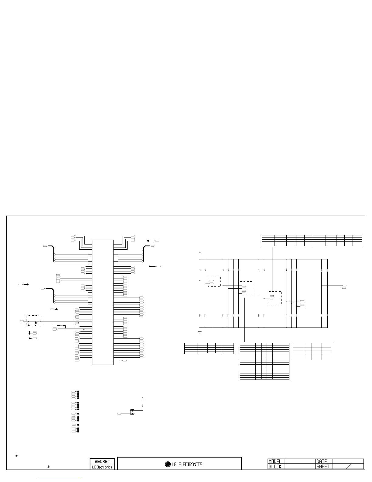
THE SYMBOL MARK OF THIS SCHEMETIC DIAGRAM INCORPORATES
SPECIAL FEATURES IMPORTANT FOR PROTECTION FROM X-RADIATION.
FIRE AND ELECTRICAL SHOCK HAZARDS, WHEN SERVICING IF IS
ESSENTIAL THAT ONLY MANUFACTURES SPECIFIED PARTS BE USED FOR
THE CRITICAL COMPONENTS IN THE SYMBOL MARK OF THE SCHEMETIC.
M14-Display In/Out
TPI_DATA[3]
FE_DEMOD1_TS_DATA[6]
FE_DEMOD1_TS_DATA[3]
FE_DEMOD1_TS_DATA[2]
TPI_DATA[7]
TPO_DATA[0]
TPI_DATA[0]
TPO_DATA[5]
FE_DEMOD1_TS_DATA[7]
TPO_DATA[6]
TPI_DATA[6]
FE_DEMOD1_TS_DATA[0]
TPO_DATA[3]
TPI_DATA[2]
TPO_DATA[1]
TPO_DATA[4]
TPO_DATA[2]
TPI_DATA[1]
TPI_DATA[5]
TPI_DATA[4]
TPO_DATA[7]
FE_DEMOD1_TS_DATA[5]
FE_DEMOD1_TS_DATA[1]
FE_DEMOD1_TS_DATA[4]
TP209
R226
100
1/16W
5%
TPI_ERR
TP210
BT_RESET
FE_DEMOD2_TS_CLK
R221 10K
DDR_3G
FE_DEMOD2_TS_CLK
GST_SOC
TXDCLKN/TX14N
TXBCLKN/TX2N
TXCCLKP/TX20P
R202 10K
BIT0_0
TXC4N/TX18N
R210 10K
BIT4_0
TXA1N/TX10N
BIT5
MODEL_OPT_10
SC_DET
TXC1P/TX22P
FE_DEMOD3_TS_SYNC
BIT1
TP203
BIT7
SC_DET
TPO_SOP
FE_DEMOD3_TS_CLK
BIT3
TPO_VAL
BIT2
FE_DEMOD2_TS_SYNC
TP213
R224
33
OPT
OPC_EN
BIT3
TP219
TPO_CLK
BIT4
COMP1_DET
FE_DEMOD2_TS_DATA
TXC2N/TX21N
TPO_ERR
TXD1N/TX16N
TXD2P/TX15P
TPO_DATA[0-7]
EO_SOC
CAM_SLIDE_DET
TP227
TXB3N/TX1NFE_DEMOD3_TS_ERROR
FE_DEMOD2_TS_VAL
FE_DEMOD3_TS_DATA
TP226
MODEL_OPT_9
FE_DEMOD2_TS_SYNC
R219 10K
DDR3_1.5GB
TPI_VAL
TXBCLKP/TX2P
BIT6
/RST_HUB
FE_DEMOD2_TS_DATA
TP204
TXC2P/TX21P
CAM_SLIDE_DET
TXB2N/TX3N
TP211
TXD1P/TX16P
LED_SCL
BIT0
R201 10K
BIT0_1
TXB4N/TX0N
FE_DEMOD1_TS_SYNC
TP221
C200
1000pF
50V
FE_DEMOD1_TS_ERROR
TPI_CLK
+3.3V_NORMAL
TPI_DATA[0-7]
R215 10K
BIT7_1
TP206
TP202
/TU_RESET1
TXC0N/TX23N
R205 10K
BIT2_1
TXB1N/TX4N
R220 10K
DDR3_2GB
EPI_SOE
TXA2N/TX9N
TPI_DATA[0-7]
FE_DEMOD1_TS_DATA[0-7]
TP208
TXD4N/TX12N
MODEL_OPT_9
TPI_SOP
TP212
TXB4P/TX0P
DEBUG
TPI_VAL
RF_SWITCH_CTL
TXA3N/TX7N
R225
33
OPT
/TU_RESET2
TP214
TXACLKN/TX8N
2D/3D_CTL
/RST_PHY
MCLK_SOC
TXA2P/TX9P
FE_DEMOD2_TS_ERROR
TP228
R203 10K
BIT1_1
LED_SDA
R206 10K
BIT2_0
FE_DEMOD3_TS_CLK
TXC3N/TX19N
TXC4P/TX18P
FE_DEMOD3_TS_DATA
TPI_ERR
TXD4P/TX12P
R209 10K
BIT4_1
TP220
TPI_CLK
BIT2
TXA3P/TX7P
TXD0N/TX17N
TXD0P/TX17P
TXA4P/TX6P
FE_DEMOD2_TS_VAL
R222 10K
NON_DDR_3G
GCLK_SOC
TPI_SOP
TXACLKP/TX8P
IR_B_RESET
BIT1
R211 10K
BIT5_1
FE_DEMOD3_TS_ERROR
TXD3N/TX13N
TP225
FE_DEMOD1_TS_VAL
CAM_TRIGGER_DET
MODEL_OPT_8
BIT4
R217 10K
DDR3_DDP
TXA4N/TX6N
R207 10K
BIT3_1
FE_DEMOD2_TS_ERROR
R212 10K
BIT5_0
MODEL_OPT_8
R214 10K
BIT6_0
TXA0N/TX11N
TXC3P/TX19P
TXC0P/TX23P
TP215
BIT5
FE_DEMOD3_TS_VAL
INSTANT_BOOT
EPI_SOE
TPO_ERR
TP207
AV1_CVBS_DET
TXA1P/TX10P
TPO_CLK
TXD2N/TX15N
TXB1P/TX4P
R223
3.3K
TXA0P/TX11P
TXC1N/TX22N
TXB0P/TX5P
BIT7
TP218
R204 10K
BIT1_0
TXD3P/TX13P
TP205
TXDCLKP/TX14P
BIT6
R208 10K
BIT3_0
TXCCLKN/TX20N
TXB3P/TX1P
TXB2P/TX3P
AMP_RESET_N
R218 10K
DDR3_NON_DDP
FE_DEMOD1_TS_CLK
TXB0N/TX5N
FE_DEMOD3_TS_VAL
BIT0
MODEL_OPT_10 EPI_LOCK8/6
TPO_DATA[0-7]
R213 10K
BIT6_1
DEBUG
R216 10K
BIT7_0
HP_DET
TPO_VAL
CAM_TRIGGER_DET
/RST_HUB
+3.3V_NORMAL
FE_DEMOD3_TS_SYNC
SW201
JTP-1127WEM
12
4
3
TPO_SOP
MODEL_OPT_11
MODEL_OPT_12
MODEL_OPT_12
MODEL_OPT_11
R227 10K
OPT
R229 10K
OPT
R228 10K
OPT
R230 10K
OPT
R231
4.7K
IC101
LG1311
TP_DVB_CLK
AH30
TP_DVB_SOP
AH32
TP_DVB_VAL
AH31
TP_DVB_ERR
AH33
TP_DVB_DATA7
AM33
TP_DVB_DATA6
AL32
TP_DVB_DATA5
AL33
TP_DVB_DATA4
AK32
TP_DVB_DATA3
AK33
TP_DVB_DATA2
AK31
TP_DVB_DATA1
AJ30
TP_DVB_DATA0
AJ31
STPI0_CLK
AL31
STPI0_SOP
AN32
STPI0_VAL
AM32
STPI0_ERR
AN31
STPI0_DATA
AM31
STPI1_CLK
AH28
STPI1_SOP
AJ28
STPI1_VAL
AK30
STPI1_ERR
AJ29
STPI1_DATA
AG27
TPI_CLK
A28
TPI_SOP
B28
TPI_VAL
B29
TPI_ERR
C28
TPI_DATA0
A27
TPI_DATA1
B27
TPI_DATA2
C27
TPI_DATA3
B26
TPI_DATA4
C26
TPI_DATA5
B25
TPI_DATA6
A25
TPI_DATA7
C25
GPIO31
AG13
GPIO30
AJ19
GPIO29
AG14
GPIO28
AG15
GPIO27
AJ15
GPIO26
AH19
GPIO25
AH18
GPIO24
AG19
GPIO23
AH5
GPIO22
AJ5
GPIO21
AJ6
GPIO20
AH6
GPIO19
AG6
GPIO18
AG5
GPIO17
AF7
GPIO16
AG7
GPIO15
AG24
GPIO14
AH16
GPIO13
V29
GPIO12
AJ21
GPIO11
AH21
GPIO10
V28
GPIO9
AG16
GPIO8
AJ24
GPIO7
AH17
GPIO6
AG17
GPIO5
AH13
GPIO4
AH15
GPIO3
AG18
GPIO2
AH14
GPIO1
AJ16
GPIO0
AH20
TPIO_CLK
D28
TPIO_SOP
E29
TPIO_VAL
E28
TPIO_ERR
F28
TPIO_DATA0
D27
TPIO_DATA1
E27
TPIO_DATA2
F27
TPIO_DATA3
E26
TPIO_DATA4
F26
TPIO_DATA5
E25
TPIO_DATA6
D25
TPIO_DATA7
F25
EPI_SOE
AA5
EPI_MCLK
AB5
EPI_GCLK
AA7
EPI_EO
AA6
EPI_VST
AB6
TX_0N
AK8
TX_0P
AL8
TX_1N
AK7
TX_1P
AL7
TX_2N
AM6
TX_2P
AN6
TX_3N
AK6
TX_3P
AL6
TX_4N
AK5
TX_4P
AL5
TX_5N
AN4
TX_5P
AN3
TX_6N
AM2
TX_6P
AM1
TX_7N
AM4
TX_7P
AM3
TX_8N
AL4
TX_8P
AL3
TX_9N
AK2
TX_9P
AK1
TX_10N
AK4
TX_10P
AK3
TX_11N
AJ4
TX_11P
AJ3
TX_12N
AH2
TX_12P
AH1
TX_13N
AH4
TX_13P
AH3
TX_14N
AG4
TX_14P
AG3
TX_15N
AF2
TX_15P
AF1
TX_16N
AF4
TX_16P
AF3
TX_17N
AE4
TX_17P
AE3
TX_18N
AD2
TX_18P
AD1
TX_19N
AD4
TX_19P
AD3
TX_20N
AC4
TX_20P
AC3
TX_21N
AB2
TX_21P
AB1
TX_22N
AB4
TX_22P
AB3
TX_23N
AA4
TX_23P
AA3
TX_LOCKN
AM8
2013.04.04
M14 Symbol B
2
MID_LG1311
31
For ISP
EPI FHD, 60Hz, V14_32 inch (6lane)
HIGH
EPI FHD, 120Hz, V13 (6 lane)
LVDS HD, 60Hz SMALL SMART
1 / 1
1 / 0
TYPE
0 / 0 / 0 / 1
LVDS FHD, 60Hz
DDR3
DDP
FRC
1 / 1 / 0 / 0
0 / 1 / 1 / 1
LVDS FHD, 120Hz
TAIWAN/COLOM
1 / 1 / 1 / 0
OLED
0 / 1 / 0 / 0
EU/CIS
0 / 1 / 1 / 0
0 / 0 / 0 / 0
0 / 1 / 0 / 1
1 / 0 / 1 / 0
0 / 0
1 / 0 / 0 / 1
PAGE 2
PANEL TYPE
BACK-END OPTIONAREA OPTION
2GB
FHD
0 / 0 / 1 / 0
Model Option
MODEL_OPT_8
1 / 0 / 1 / 1
EPI FHD, 120Hz, v14_32inch (6 lane)
Vby1 FHD, 120Hz
1.5GB
BIT[2/3/4/5]DVB
LVDS FHD, 60Hz, CP BOX
1 / 0 / 0 / 0
NON_DDP
EPI FHD, 120Hz, V12 (6 lane)
LOW
1 / 1 / 0 / 1
LVDS HD, 60Hz
DDR3
MODEL_OPT_10
BIT [0/1]
0 / 1
ATSC
0 / 0 / 1 / 1
JP
CHINA/HONGKONG
MODEL_OPT_9
1 / 1 / 1 / 1
EPI FHD, 120Hz, V14 (8 lane)
Near AMP
ASIA/AFRICA
KOREA
N/AMERICA
S/AMERCIA
JAPAN
TAIWAN/COL
T/C
1 / 1
T2/C
BIT [6/7]
1 / 0
0 / 1
T2/C/S2/ATV_SOC
AJJA
0 / 0
T2/C/S2/ATV_EXT
EU/CIS
CHINA/HONG
T/C
T2/C/ATV_SOC
T2/C/S2
DDR3 3G
NON_DDR3 3G
FOR UD
T/C
T2/C
T2/C PIP
Default Default
ISDB
BRAZILKOREA
ISDB PIP
ATSC PIP
ATV_EXT
JAPAN
ATV_SOC
NORTH AMERICA
ATSC PIP
ATV_SOC
ATV_EXT
MODEL_OPT_11
MODEL_OPT_12
LVDS FHD, 120Hz OLED
T2/C/ATV_EXT
Copyright ⓒ 2014 LG Electronics. Inc. All right reserved.
Only for training and service purposes
LGE Internal Use Only
 Loading...