

Page 1

LCD TV
SERVICE MANUAL
CAUTION
BEFORE SERVICING THE CHASSIS,
READ THE SAFETY PRECAUTIONS IN THIS MANUAL.
CHASSIS : ML-051A
MODEL : 37LP1R-ME
website:http://biz.LGservice.com
e-mail:http://www.LGEservice.com/techsup.html
Page 2

- 2 -
CONTENTS
CONTENTS .............................................................................................. 2
PRODUCT SAFETY ..................................................................................3
SPECIFICATION........................................................................................6
ADJUSTMENT INSTRUCTION................................................................11
TROUBLE SHOOTING............................................................................15
BLOCK DIAGRAM...................................................................................18
WIRING DIAGRAM..................................................................................19
EXPLODED VIEW .................................................................................. 20
EXPLODED VIEW PARTS LIST..............................................................21
REPLACEMENT PARTS LIST ............................................................... 22
SVC. SHEET ...............................................................................................
Page 3
- 3 -
SAFETY PRECAUTIONS
Many electrical and mechanical parts in this chassis have special safety-related characteristics. These parts are identified by in the
Schematic Diagram and Replacement Parts List.
It is essential that these special safety parts should be replaced with the same components as recommended in this manual to prevent
Shock, Fire, or other Hazards.
Do not modify the original design without permission of manufacturer.
General Guidance
An isolation Transformer should always be used during the
servicing of a receiver whose chassis is not isolated from the AC
power line. Use a transformer of adequate power rating as this
protects the technician from accidents resulting in personal injury
from electrical shocks.
It will also protect the receiver and it's components from being
damaged by accidental shorts of the circuitry that may be
inadvertently introduced during the service operation.
If any fuse (or Fusible Resistor) in this TV receiver is blown,
replace it with the specified.
When replacing a high wattage resistor (Oxide Metal Film Resistor,
over 1W), keep the resistor 10mm away from PCB.
Keep wires away from high voltage or high temperature parts.
Before returning the receiver to the customer,
always perform an AC leakage current check on the exposed
metallic parts of the cabinet, such as antennas, terminals, etc., to
be sure the set is safe to operate without damage of electrical
shock.
Leakage Current Cold Check(Antenna Cold Check)
With the instrument AC plug removed from AC source, connect an
electrical jumper across the two AC plug prongs. Place the AC
switch in the on position, connect one lead of ohm-meter to the AC
plug prongs tied together and touch other ohm-meter lead in turn to
each exposed metallic parts such as antenna terminals, phone
jacks, etc.
If the exposed metallic part has a return path to the chassis, the
measured resistance should be between 1MΩ and 5.2MΩ.
When the exposed metal has no return path to the chassis the
reading must be infinite.
An other abnormality exists that must be corrected before the
receiver is returned to the customer.
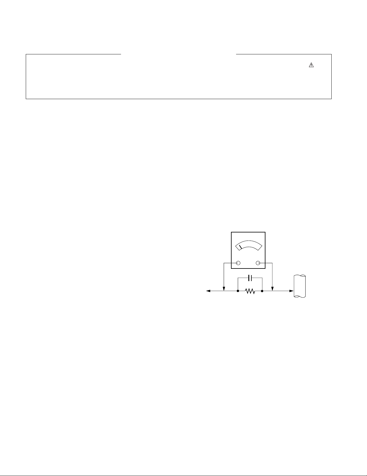
Leakage Current Hot Check (See below Figure)
Plug the AC cord directly into the AC outlet.
Do not use a line Isolation Transformer during this check.
Connect 1.5K/10watt resistor in parallel with a 0.15uF capacitor
between a known good earth ground (Water Pipe, Conduit, etc.)
and the exposed metallic parts.
Measure the AC voltage across the resistor using AC voltmeter
with 1000 ohms/volt or more sensitivity.
Reverse plug the AC cord into the AC outlet and repeat AC voltage
measurements for each exposed metallic part. Any voltage
measured must not exceed 0.75 volt RMS which is corresponds to
0.5mA.
In case any measurement is out of the limits specified, there is
possibility of shock hazard and the set must be checked and
repaired before it is returned to the customer.
Leakage Current Hot Check circuit
IMPORTANT SAFETY NOTICE
0.15uF
To Instrument's
exposed
METALLIC PARTS
AC Volt-meter
Good Earth Ground
such as WATER PIPE,
CONDUIT etc.
1.5 Kohm/10W
Page 4

- 4 -
CAUTION: Before servicing receivers covered by this service
manual and its supplements and addenda, read and follow the
SAFETY PRECAUTIONS on page 3 of this publication.
NOTE: If unforeseen circumstances create conflict between the
following servicing precautions and any of the safety precautions on
page 3 of this publication, always follow the safety precautions.
Remember: Safety First.
General Servicing Precautions
1. Always unplug the receiver AC power cord from the AC power
source before;
a. Removing or reinstalling any component, circuit board
module or any other receiver assembly.
b. Disconnecting or reconnecting any receiver electrical plug or
other electrical connection.
c. Connecting a test substitute in parallel with an electrolytic
capacitor in the receiver.
CAUTION: A wrong part substitution or incorrect polarity
installation of electrolytic capacitors may result in an
explosion hazard.
2. Test high voltage only by measuring it with an appropriate high
voltage meter or other voltage measuring device (DVM,
FETVOM, etc) equipped with a suitable high voltage probe.
Do not test high voltage by "drawing an arc".
3. Do not spray chemicals on or near this receiver or any of its
assemblies.
4. Unless specified otherwise in this service manual, clean
electrical contacts only by applying the following mixture to the
contacts with a pipe cleaner, cotton-tipped stick or comparable
non-abrasive applicator; 10% (by volume) Acetone and 90% (by
volume) isopropyl alcohol (90%-99% strength)
CAUTION: This is a flammable mixture.
Unless specified otherwise in this service manual, lubrication of
contacts in not required.
5. Do not defeat any plug/socket B+ voltage interlocks with which
receivers covered by this service manual might be equipped.
6. Do not apply AC power to this instrument and/or any of its
electrical assemblies unless all solid-state device heat sinks are
correctly installed.
7. Always connect the test receiver ground lead to the receiver
chassis ground before connecting the test receiver positive
lead.
Always remove the test receiver ground lead last.
8. Use with this receiver only the test fixtures specified in this
service manual.
CAUTION: Do not connect the test fixture ground strap to any
heat sink in this receiver.
Electrostatically Sensitive (ES) Devices
Some semiconductor (solid-state) devices can be damaged easily
by static electricity. Such components commonly are called
Electrostatically Sensitive (ES) Devices. Examples of typical ES
devices are integrated circuits and some field-effect transistors and
semiconductor "chip" components. The following techniques
should be used to help reduce the incidence of component
damage caused by static by static electricity.
1. Immediately before handling any semiconductor component or
semiconductor-equipped assembly, drain off any electrostatic
charge on your body by touching a known earth ground.
Alternatively, obtain and wear a commercially available
discharging wrist strap device, which should be removed to
prevent potential shock reasons prior to applying power to the
unit under test.
2. After removing an electrical assembly equipped with ES
devices, place the assembly on a conductive surface such as
aluminum foil, to prevent electrostatic charge buildup or
exposure of the assembly.
3. Use only a grounded-tip soldering iron to solder or unsolder ES
devices.
4. Use only an anti-static type solder removal device. Some solder
removal devices not classified as "anti-static" can generate
electrical charges sufficient to damage ES devices.
5. Do not use freon-propelled chemicals. These can generate
electrical charges sufficient to damage ES devices.
6. Do not remove a replacement ES device from its protective
package until immediately before you are ready to install it.
(Most replacement ES devices are packaged with leads
electrically shorted together by conductive foam, aluminum foil
or comparable conductive material).
7. Immediately before removing the protective material from the
leads of a replacement ES device, touch the protective material
to the chassis or circuit assembly into which the device will be
installed.
CAUTION: Be sure no power is applied to the chassis or circuit,
and observe all other safety precautions.
8. Minimize bodily motions when handling unpackaged
replacement ES devices. (Otherwise harmless motion such as
the brushing together of your clothes fabric or the lifting of your
foot from a carpeted floor can generate static electricity
sufficient to damage an ES device.)
General Soldering Guidelines
1. Use a grounded-tip, low-wattage soldering iron and appropriate
tip size and shape that will maintain tip temperature within the
range or 500
F to 600 F.
2. Use an appropriate gauge of RMA resin-core solder composed
of 60 parts tin/40 parts lead.
3. Keep the soldering iron tip clean and well tinned.
4. Thoroughly clean the surfaces to be soldered. Use a mall wirebristle (0.5 inch, or 1.25cm) brush with a metal handle.
Do not use freon-propelled spray-on cleaners.
5. Use the following unsoldering technique
a. Allow the soldering iron tip to reach normal temperature.
(500
F to 600 F)
b. Heat the component lead until the solder melts.
c. Quickly draw the melted solder with an anti-static, suction-
type solder removal device or with solder braid.
CAUTION: Work quickly to avoid overheating the
circuitboard printed foil.
6. Use the following soldering technique.
a. Allow the soldering iron tip to reach a normal temperature
(500
F to 600 F)
b. First, hold the soldering iron tip and solder the strand against
the component lead until the solder melts.
c. Quickly move the soldering iron tip to the junction of the
component lead and the printed circuit foil, and hold it there
only until the solder flows onto and around both the
component lead and the foil.
CAUTION: Work quickly to avoid overheating the circuit
board printed foil.
d. Closely inspect the solder area and remove any excess or
splashed solder with a small wire-bristle brush.
SERVICING PRECAUTIONS
Page 5

- 5 -
IC Remove/Replacement
Some chassis circuit boards have slotted holes (oblong) through
which the IC leads are inserted and then bent flat against the
circuit foil. When holes are the slotted type, the following technique
should be used to remove and replace the IC. When working with
boards using the familiar round hole, use the standard technique
as outlined in paragraphs 5 and 6 above.
Removal
1. Desolder and straighten each IC lead in one operation by gently
prying up on the lead with the soldering iron tip as the solder
melts.
2. Draw away the melted solder with an anti-static suction-type
solder removal device (or with solder braid) before removing the
IC.
Replacement
1. Carefully insert the replacement IC in the circuit board.
2. Carefully bend each IC lead against the circuit foil pad and
solder it.
3. Clean the soldered areas with a small wire-bristle brush.
(It is not necessary to reapply acrylic coating to the areas).
"Small-Signal" Discrete Transistor
Removal/Replacement
1. Remove the defective transistor by clipping its leads as close as
possible to the component body.
2. Bend into a "U" shape the end of each of three leads remaining
on the circuit board.
3. Bend into a "U" shape the replacement transistor leads.
4. Connect the replacement transistor leads to the corresponding
leads extending from the circuit board and crimp the "U" with
long nose pliers to insure metal to metal contact then solder
each connection.
Power Output, Transistor Device
Removal/Replacement
1. Heat and remove all solder from around the transistor leads.
2. Remove the heat sink mounting screw (if so equipped).
3. Carefully remove the transistor from the heat sink of the circuit
board.
4. Insert new transistor in the circuit board.
5. Solder each transistor lead, and clip off excess lead.
6. Replace heat sink.
Diode Removal/Replacement
1. Remove defective diode by clipping its leads as close as
possible to diode body.
2. Bend the two remaining leads perpendicular y to the circuit
board.
3. Observing diode polarity, wrap each lead of the new diode
around the corresponding lead on the circuit board.
4. Securely crimp each connection and solder it.
5. Inspect (on the circuit board copper side) the solder joints of
the two "original" leads. If they are not shiny, reheat them and if
necessary, apply additional solder.
Fuse and Conventional Resistor
Removal/Replacement
1. Clip each fuse or resistor lead at top of the circuit board hollow
stake.
2. Securely crimp the leads of replacement component around
notch at stake top.
3. Solder the connections.
CAUTION: Maintain original spacing between the replaced
component and adjacent components and the circuit board to
prevent excessive component temperatures.
Circuit Board Foil Repair
Excessive heat applied to the copper foil of any printed circuit
board will weaken the adhesive that bonds the foil to the circuit
board causing the foil to separate from or "lift-off" the board. The
following guidelines and procedures should be followed whenever
this condition is encountered.
At IC Connections
To repair a defective copper pattern at IC connections use the
following procedure to install a jumper wire on the copper pattern
side of the circuit board. (Use this technique only on IC
connections).
1. Carefully remove the damaged copper pattern with a sharp
knife. (Remove only as much copper as absolutely necessary).
2. carefully scratch away the solder resist and acrylic coating (if
used) from the end of the remaining copper pattern.
3. Bend a small "U" in one end of a small gauge jumper wire and
carefully crimp it around the IC pin. Solder the IC connection.
4. Route the jumper wire along the path of the out-away copper
pattern and let it overlap the previously scraped end of the good
copper pattern. Solder the overlapped area and clip off any
excess jumper wire.
At Other Connections
Use the following technique to repair the defective copper pattern
at connections other than IC Pins. This technique involves the
installation of a jumper wire on the component side of the circuit
board.
1. Remove the defective copper pattern with a sharp knife.
Remove at least 1/4 inch of copper, to ensure that a hazardous
condition will not exist if the jumper wire opens.
2. Trace along the copper pattern from both sides of the pattern
break and locate the nearest component that is directly
connected to the affected copper pattern.
3. Connect insulated 20-gauge jumper wire from the lead of the
nearest component on one side of the pattern break to the lead
of the nearest component on the other side.
Carefully crimp and solder the connections.
CAUTION: Be sure the insulated jumper wire is dressed so the
it does not touch components or sharp edges.
Page 6
- 6 -
1. Application range
This specification is applied to ML-051A chassis.
2. Requirement for Test
Testing for standard of each part must be followed in below
condition.
(1) Temperature: 25°C ± 2°C
(2) Humidity: 65% ± 10%
(3) Power: Standard input voltage (AC 100-240V, 50/60Hz)
(4) Measurement must be performed after heat-run more than
30min.
(5) Adjusting standard for this chassis is followed a special
standard.
SPECIFICATION
NOTE : Specifications and others are subject to change without notice for improvement
.
3.General Specification(TV)
No Item Specification Remark
1. Video input applicable system PAL-D/K, B/G, I, NTSC-M, SECAM
NTSC 4.43
2. Receivable Broadcasting System 1) PAL/SECAM BG (ZE/TE)
2) PAL/SECAM DK EU/Non-EU
3) PAL I/I (PAL Market)
4) SECAM L/L'
5) NTSC M
6) PAL-N/M 6),7) South America Market
7) NTSC M
7) Except South America NTSC Market (ME)
3. RF Input Channel VHF : E2 ~ E12 PAL
UHF : E21 ~ E69
CATV : S1 ~ S20
HYPER : S21~ S47
L/L' : B, C, D FRANCE
VHF : 2~13 NTSC
UHF : 14~69
CATV : 1~125
VHF Low : 1 ~ M10 JAPAN
VHF High : 4~S22
UHF : S23~62
4. Input Voltage AC 100 ~ 240 V/50Hz, 60Hz
5. Market Worldwide
6. Picture Size 800.4mm 37 inch
7. Tuning System FVS 100 program PAL,200 PR.(Option)
FS NTSC
8. Operating Environment 1) Temp : 0 ~ 40 deg
2) Humidity : 10~85 %
9. Storage Environment 3) Temp : -20 ~ 60 deg
4) Humidity : 10~85 %
10. Display LCD Module LPL
Page 7
- 7 -
4. General Specification
No Item Specification Unit Remark
1 Panel 32" TFT WXGA LCD
2 Frequency range H : 31 ~ 61Khz PC Input
V : 56 ~ 75Hz
3 Control Function 1) Contrast/Brightness
2) H-Position / V-Position
3) Tracking : Clock / Phase
4) Auto Configure
5) Reset
4 Component Jack 1 : Y Middle east
3 : Pb / NTSC Area
5 : Pr
7 : Line1 Ready
9 : LINE2
11: LINE3
13: Line3 Ready
D4 Jack 2 : Y GND JAPAN Only
(525i,525p,750p,1125i) 4 : Pb GND
6 : Pr GND
8 : LINE1
10:Line2 Ready
12:SWITCH GND
14: SWITCH
5 H/V-Sync Video Power consumption LED
Power ON ON/ON Active
≤
max 190W W Green
Stand by OFF/ON OFF
≤
3.0W W Red
DPMS Mode ON/OFF OFF
≤
typ. 30W W Green
Power off - - - W *
6 LCD Module Type Size LPL 877.0 x 516.8 x 55.5 mm (H) x (V) x (D)
Pixel Pitch LPL 0.200 x 0.600 x RGB
Pixel Format 1366 horiz. By 768 vert. Pixels
RGB strip arrangement
Coating Hard coating(3H), Anti-glare
treatment of the front polarizer,
Back Light LPL 16CCFL
Page 8
- 8 -
5.Optical Feature(LCD Module)
Item RemarkSpecification
Viewing Angle
<CR
10>
Luminance
Contrast Ratio
CIE Color Coordinates
Typical
MAX/MIN
ALL white/All back
LPL
R/L, U/D
Luminance(cd/
)
Variation
Typ
176, 176
500
600
0.285
0.293
0.640
0.341
0.287
0.610
0.146
0.069
WHITE
RED
GREEN
BLUE
W
x
W
y
R
R
y
G
x
G
y
B
x
B
y
Typ.
Typ.
Typ.
Typ.
Typ.
Typ.
Typ.
Typ.
No.
1
2
3
4
6.Component Video Input (Y, PB, PR)
No
Specification
Proposed
Resolution H-freq(kHz) V-freq(Hz)
1. 640x480 15.73 60 SDTV, DVD 480i ZE, TE, ME
2. 640x480 15.63 59.94 SDTV, DVD 480i ZE, TE, ME
3. 704x480 31.47 59.94 EDTV 480p TE, ME
4. 720x576 15.625 50.00 SDTV, DVD 625 Line ZE, TE, ME
5. 720x576 31.25 50.00 HDTV 576p TE, ME
6. 1280x720 45.00 60.00 HDTV 720p TE, ME
7. 1280x720 44.96 59.94 HDTV 720p TE, ME
8. 1920x1080 31.25 50.00
HDTV 1080i 50Hz (AU Ver.)
TE, ME
9. 1920x1080 33.75 60.00
HDTV 1080i 60Hz (ATSC)
TE, ME
10. 1920x1080 33.72 59.94 HDTV 1080i 59.94Hz TE, ME
7. PC INPUT Mode Table
No Resolution H-freq(kHz) V-freq.(Hz) Pixel clock(MHz) Proposed
Analog RGB, Digital RGB
1 720x400 31.468 70.8 28.321
2 640x480 31.469 59.94 25.17 VESA
37.684 75.00 31.5 VESA
3 800x600 37.879 60.31 40.00 VESA
46.875 75 49.5 VESA
4 832x624 49.725 74.55 57.283
5 1024x768 48.363 60.00 65.00 VESA(XGA)
56.47 70.00 75.00 VESA(XGA)
60.123 75.029 78.75 VESA(XGA)
6 1280x768 47.776 59.870 79.50 VESA(WXGA)
7 1360x768 47.720 59.799 84.75 VESA(WXGA)
8 1366x768 47.720 59.799 84.75 Supported
9 1920x1080 33.75 60.00 86.375 HDCP DVI Digital 1080i
10 1280x720 45.00 60.00 74.375 HDCP DVI Digital 720p
Min
400
Typ.
-0.03
Max
Typ.
+0.03
Page 9
- 9 -
8. HDMI INPUT Mode Table
9. Mechanical specification
<Table 1> Scart Arrangement 1.(Full Scart)
No Resolution H-freq(kHz) V-freq.(Hz) Pixel clock(MHz) Proposed
Analog RGB, Digital RGB
1 720x400 31.468 70.8 28.321
2 640x480 31.469 59.94 25.17 VESA
37.684 75.00 31.5 VESA
3 800x600 37.879 60.31 40.00 VESA
46.875 75 49.5 VESA
4 832x624 49.725 74.55 57.283
5 1024x768 48.363 60.00 65.00 VESA(XGA)
56.47 70.00 75.00 VESA(XGA)
60.123 75.029 78.75 VESA(XGA)
6 1280x768 47.776 59.870 79.50 VESA(WXGA)
7 1360x768 47.720 59.799 84.75 VESA(WXGA)
8 1366x768 47.720 59.799 84.75 Supported
9 1920x1080 33.75 60.00 86.375 HDCP DVI Digital 1080i
10 1280x720 45.00 60.00 74.375 HDCP DVI Digital 720p
Pin Signal Signal Level Impedance
1 Audio Output B (right) 0.5 Vrms < 1
2 Audio Input B (right) 0.5 Vrms > 10
3 Audio Output A (left) 0.5 Vrms < 1
4 Ground (audio) - 5 Ground (blue) - 6 Audio input A (left) 0.5 Vrms > 10
7 Blue input 0.7 V 75
8 Function Select (AV control) High (9.5 - 12V) - AV Mode
Mid (5 - 8V) - Wide Screen
Low (0 - 2V) - TV Mode > 10
9 Ground (Green) - 10 Comms Data 2
11 Green input 0.7 V 75
12 Comms Data 1
13 Ground (Red) - 14 Ground (Blanking) - 15 Red input 0.7 V 75
16 RGB Switching Control High (1 - 3V) - RGB
Low (0 - 0.4V) - Composite 75
17 Ground (Video input & Output) - 18 Ground (RGB Switching Control) - 19 Video output (Composite) 1V including sync 75
20 Video input (Composite) 1V including sync 75
21 Common ground (Shield) - -
Page 10
- 10 -
<Table 2> Scart Arrangement 2.(Half Scart)
Pin Signal Signal Level Impedance
1 Audio Output B (right) 0.5 Vrms < 1
2 Audio Input B (right) 0.5 Vrms > 10
3 Audio Output A (left) 0.5 Vrms < 1
4 Ground (audio) - 5 Ground (blue) - 6 Audio input A (left) 0.5 Vrms > 10
7- - 8 Function Select (AV control) High (9.5 - 12V) - AV Mode
Mid (5 - 8V) - Wide Screen
Low (0 - 2V) - TV Mode > 10
9 Ground (Green) - 10 Comms Data 2
11 - - 12 Comms Data 1
13 Ground (Red) - 14 Ground (Blanking) - 15 Red input
16 - - 17 Ground (Video input & Output) - 18 - - 19 Video output (Composite) 1V including sync 75
20 Video input (Composite) 1V including sync 75
21 Common ground (Shield) - -
Page 11

- 11 -
ADJUSTMENT INSTRUCTION
1. Application Range
This spec. sheet is applied to all of the ML-051A chassis
(TORNADO) manufactured at LG TV Plant
2. Specification.
2.1 Because this is not a hot chassis, it is not necessary to
use an isolation transformer. However, the use of
isolation transformer will help to protect test
instruments.
2.2 Adjustment must be done in the correct sequence.
2.3 The adjustment must be performed at 25±5°C
temperature and 65±10% relative humidity if there is
no specified designation.
2.4 The input voltage of the receiver must be kept between
100~220V, 50/60Hz.
2.5 Before adjustment, execute Heat-Run for 30 minutes
at RF no signal.
3. EDID
* Caution
- Use the proper signal cable for EDID Download
Analog EDID: Pin3 exists
Digital EDID: Pin3 exists
Caution: - Never connect HDMI & DVI-D & DVI-A Cable
at the same time.
- Use the proper cables below for EDID Writing
3.1 Data
3.1.1 ANALOG(128Bytes)
3.2.2 DIGITAL(128Bytes)
3.2.3 EDID FOR HDMI(256Bytes)
3.2.4 Detail EDID Options are below(a, b, c, d, e)
a. Product ID
b. Serial No : Controlled on production line
c. Month, Year : Controlled on production line
d. Model Name(Hex) :
e. Checksum: ChangeSable by total EDID data
00 01 02 03 04 05 06 07 08 09 0A 0B 0C 0D 0E 0F
00 00 FF FF FF FF FF FF 00 1E 6D
10 01 03 80 46 27 78 EA D9 B0 A3 57 49 9C 25
20 11 49 4B A5 6E 80 31 40 01 01 01 01 45 40 01 01
30 61 40 01 01 01 01 1B 21 50 A0 51 00 1E 30 48 88
40 35 00 BC 88 21 00 00 1C 4E 1F 00 80 51 00 1E 30
50 40 80 37 00 BC 88 21 00 00 18 00 00 00 FC 00 33
60 0A 20 20 20 00 00 00 FD
70 00 38 4B 1F 3D 09 00 0A 20 20 20 20 20 20 00
00 01 02 03 04 05 06 07 08 09 0A 0B 0C 0D 0E 0F
00 00 FF FF FF FF FF FF 00 1E 6D
10 01 03 80 46 27 78 EA D9 B0 A3 57 49 9C 25
20 11 49 4B A5 6E 80 31 40 01 01 01 01 45 40 01 01
30 61 40 01 01 01 01 1B 21 50 A0 51 00 1E 30 48 88
40 35 00 BC 88 21 00 00 1C 4E 1F 00 80 51 00 1E 30
50 40 80 37 00 BC 88 21 00 00 18 00 00 00 FC 00 33
60 0A 20 20 20 00 00 00 FD
70 00 38 4B 1F 3D 09 00 0A 20 20 20 20 20 20 01
00 01 02 03 04 05 06 07 08 09 0A 0B 0C 0D 0E 0F
00 02 03 21 1C 46 85 04 02 01 03 00 23 09 07 07 23
10 09 07 07 23 09 07 07 83 01 00 00 65 03 0C 00 10
20 00 01 1D 00 80 51 D0 1C 20 40 80 35 00 BC 88 21
30 00 00 1E 8C 0A D0 8A 20 E0 2D 10 10 3E 96 00 13
40 8E 21 00 00 18 2A 12 00 10 41 43 17 20 28 60 35
50 00 00 00 32 00 00 1C 00 00 00 00 00 00 00 00 00
60 00 00 00 00 00 00 00 00 00 00 00 00 00 00 00 00
70 00 00 00 00 00 00 00 00 00 00 00 00 00 00 00 1E
00 01 02 03 04 05 06 07 08 09 0A 0B 0C 0D 0E 0F
00 00 FF FF FF FF FF FF 00 1E 6D
10 01 03 01 46 27 78 EA D9 B0 A3 57 49 9C 25
20 11 49 4B A5 6E 80 31 40 01 01 01 01 45 40 01 01
30 61 40 01 01 01 01 1B 21 50 A0 51 00 1E 30 48 88
40 35 00 BC 88 21 00 00 1C 4E 1F 00 80 51 00 1E 30
50 40 80 37 00 BC 88 21 00 00 18 00 00 00 FD 00 38
60 4B 1F 3D 09 00 0A 20 20 20 20 20 20 00 00 00 FC
70 0A 20 20 20 00
No Item Content Hexadecimal
1 Manufacturer ID GSM 1E6D
2 Version Digital 1 01
3 Revision Digital 3 03
a
e
e
c
c
c
d
d
e
d
b
a
b
a b
Model name Product ID
Product ID
Dec Hex
EDID Table
26LX2R
22039(A) 22039(A) 5617 1756
22040(A) 22040(D) 5618 1856
32LX2R
30041(A) 30041(A) 7559 5975
30042(D) 30042(D) 755A 5A75
32LP1R
30039(A) 30039(A) 7557 5775
30040(D) 30040(D) 7558 5875
37LP1R
30043(A) 30043(A) 755B 5B75
30044(D) 30044(D) 755C 5C75
42LP1R
40013(A) 40013(A) 9C4D 4D9C
40014(D) 40014(D) 9C4E 4E9C
Model Name Model Name(HEX)
26LX2R-ZE 32364C5832522D5A45
32LX2R-ZE 33324C5832522D5A45
32LP1R-ZE 33324C5031522D5A45
37LP1R-ZE 33374C5031522D5A45
42LP1R-ZE 34324C5031522D5A45
Page 12
- 12 -
4. ADC Calibration
4.1 Adjustment of RF/AV/SAV
* Test Equipment
- Remote controller for adjustment
- MSPG-925F Pattern Generator->Model: 202 / Pattern: 32
4.1.1 Method of Auto RF/AV/S-VIDEO Color Balance.
1) Input the Video Signal: 75% Color Bar signal into AV3
(ZE), AV1(TE), VIDEO1(ME)
2) Set the PSM to Standard mode in the Picture menu.
3) Press ADJ key on R/C for adjustment.
4) Press the
(Vol. +) key to operate the set, then it
becomes automatically.
5) Auto-RGB OK means the adjustment is completed.
4.2 Adjustment of Component.
* Required Equipments
- Remote controller for adjustment
- MSPG-925F Pattern Generator->Model: 215 / Pattern: 33
4.2.1Method of Auto Component Color Balance
1) Input the Component 720p 100% Color Bar(MSPG925F model:215, pattern:33) signal into Component.
(ZE : component , TE/ME : component 1 or 2)
2) Set the PSM to Standard mode in the Picture menu.
3) Press the ADJ key on R/C for adjustment.
4) Press the
(Vol. +) key to operate the set , then it
becomes automatically.
5) Auto-RGB OK means the adjustment is completed.
4.3 Adjustment of RGB
* Required Equipments
- Remote controller for adjustment
- MSPG-925F Pattern Generator
4.3.1Method of Auto RGB Color Balance
1) Input the PC 1024x768@60Hz 1/2 Black & White
Pattern(MSPG-925F model:37, pattern:18) into RGB.
(using D-sub to DVI-I cable)
2) Set the PSM to Standard mode in Picture menu.
3) Press the ADJ key on R/C for adjustment.
4) Press the
(Vol. +) key operate To set , then it
becomes automatically.
5) Auto-RGB OK means adjustment is completed.
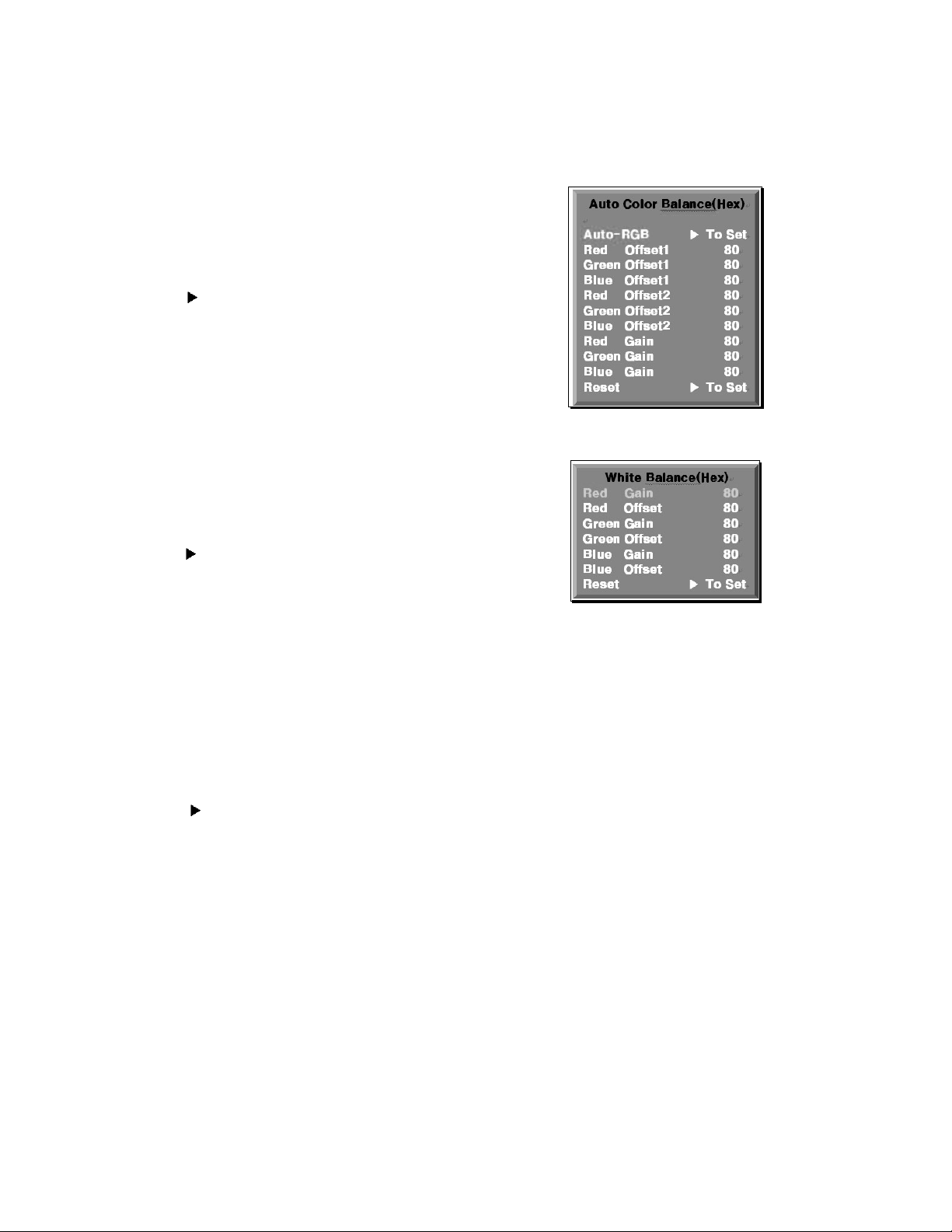
5. white Balance
5.1 Manual white Balance (AV)
1) Execute CA-110 Zero Calibration.
2) Execute the SET Heat Run for 30minutes
3) Push the ADJ Button then you can see the OSD
4) Push the ADJ Button again for White Balance mode
5) Adjust High light with R/B Gain/Offset(G Gain fix, G
Offset fix)
Page 13

- 13 -
6. Shipping Conditions
No Item Condition Remark
1 Power Off
2 Volume Level 30
3 Main Picture Input TV
4 Main Last Channel Pr 01
5 Mute Off
6 ARC 16 : 9
7 Station Auto Program
Manual Program
Program Edit
Favorite Program None
8 Picture PSM Dynamic
Dynamic Contrast 100
Brightness 45
Colour 50
Sharpness 50
9 Sound SSM Flat
AVL Off
Balance 0
10 Special Input TV
Child Lock Off
Auto sleep Off
Language English(Area Management)
11 PC H-Position
V-Position Variable by each mode
Clock
Phase
Auto Configue
Page 14

- 14 -
SVC REMOCON
1 POWER
2 POWER ON
3 MUTE
4 P-CHECK
5 S-CHECK
6 ARC
7 CAPTION
8 TXT
9 TV/AV
10 TURBO SOUND
11 TURBO PICTURE
12 IN-START
13 ADJ
14 MPX
15 EXIT
16 APC(PSM)
17 ASC(SSM)
18 MULTIMIDIA
19 FRONT-AV
20 CH
21 VOL
22 ENTER
23 PIP CH-(OP1)
24 PIP CH+(OP2)
25 PIP SWAP(OP3)
26 PIP INPUT(OP4)
27 EYE
28 MENU
29 IN-STOP
30 STILL
31 TIME
32 SIZE
33 MULTI PIP
34 POSITION
35 MODE
36 PIP
37 TILT
38 0~9
To turn the TV on or off
To turn the TV on automatically if the power is supplied to the TV. (Use the
POWER key to deactivate): It should be deactivated when delivered.
To activate the mute function.
To check TV screen image easily.
To check TV screen sound easily
To select size of the main screen (Normal, Spectacle, Wide or Zoom)
Switch to closed caption broadcasting
To toggle on/off the teletext mode
To select an external input for the TV screen
To start turbo sound
To start turbo picture
To enter adjustment mode when manufacturing the TV sets.
To adjust the screen voltage (automatic):
In-start
mute Adjust AV(Enter into W/B adjustment mode)
W/B adjustment (automatic):
After adjusting the screen W/B adjustment Exit two times (Adjustment completed)
To enter into the adjustment mode. To adjust horizontal line and sub-brightness.
To select the multiple sound mode (Mono, Stereo or Foreign language)
To release the adjustment mode
To easily adjust the screen according to surrounding brightness
To easily adjust sound according to the program type
To check component input
To check the front AV
To move channel up/down or to select a function displayed on the screen.
To adjust the volume or accurately control a specific function.
To set a specific function or complete setting.
To move the channel down in the PIP screen.
To use as a red key in the teletext mode
To move the channel in the PIP screen
To use as a green key in the teletext mode
To switch between the main and sub screens
To use as a yellow key in the teletext mode
To select the input status in the PIP screen
To use as a blue key in the teletext mode
To set a function that will automatically adjust screen status to match
the surrounding brightness so natural color can be displayed.
To select the functions such as video, voice, function or channel.
To set the delivery condition status after manufacturing the TV set.
To halt the main screen in the normal mode, or the sub screen at the PIP screen.
Used as a hold key in the teletext mode (Page updating is stopped.)
Displays the teletext time in the normal mode
Enables to select the sub code in the teletext mode
Used as the size key in the PIP screen in the normal mode
Used as the size key in the teletext mode
Used as the index key in the teletext mode (Top index will be
displayed if it is the top text.)
To select the position of the PIP screen in the normal mode
Used as the update key in the teletext mode (Text will be
displayed if the current page is updated.)
Used as Mode in the teletext mode
To select the simultaneous screen
To adjust screen tilt
To manually select the channel.
Shortcut keys
Shortcut keys
Shortcut keys
Use the AV
key to enter
the screen
W/B
adjustment
mode.
Shortcut keys
Shortcut keys
Shortcut keys
Page 15

- 15 -
TROUBLESHOOTING
NO POWER
(POWER INDICATOR OFF)
REPLACE POWER BOARD
CHECK POWER BOARD
CHECK CN804
VOLTAGE (P-ST_5V)
No
CHECK CRYSTAL X800
CHECK CRYCTAL
X800(19.6608MHZ)
No
Yes
CHECK IC806
CHECK IC806 VOLTAGE (5V)
No
Yes
CHECK Q1001
CHECK Power on/off
(5V)
No
Yes
Yes
Page 16

- 16 -
NO VIDEO
REPLACE LCD MODULE
CHECK THE PERIPHERAL
IC800
CHECK LVDS Output
P3(PIN 21, PIN 22)
No
CHECK THE PERIPHERAL
IC1
DOWN LOAD ISP DATA
or REPLACE MAIN BOARD
Check L2
(12V)
No
Yes
CHECK L1022
(24V)
CHECK R898
(3.3V)
No
Yes
Yes
Yes No
Page 17

- 17 -
NO SOUND
REPLACE JACK BOARD
INSERT CABLES WELL
IS THE SPK CABLE
CONNECTED WELL?
No
CHECK IC302 OR CHANGE
DOES IC302 OPERATE?
No
Yes
CHECK IC301 OR CHANGE
DOES IC301 OPERATE?
No
Yes
CHECK X300 OR CHANGE
DOES IC300 OPERATE?
DOES IC400 OPERATE?
No
Yes
Yes
Yes
CHECK X400 OR CHANGE
No
Page 18

BLOCK DIAGRAM
- 18 -
Page 19

- 19 -
6
WIRING DIAGRAM
NO. PART NO.
1
2
3
4
5
6631V10004A
6631T12006Q
6631T20028V
6631T20036G
6631T20034V
6
7
8
9
10
6631T20032H
6631T20032H
6631T25024V
6631T25024X
6631T25023G
111213
14
6631T20033D
6631T20034U
6631T11020Z
6631T11023D
NO. PART NO. NO. PART NO.
8
5
4
13
1 1
3
14
9
7
10
12
2
11
Page 20

- 20 -
EXPLODED VIEW
130
030
050
140
120
100
060
020
080
090
070
110
190
180
160 170
150
040
010
Page 21

- 21 -
EXPLODED VIEW PARTS LIST
No.
PART NO.
DESCRIPTION
3091TKE028G CABINET ASSEMBLY, 37LP1R-ME BRAND . CABINET ASSY(SET)
6304FLP291A LCD(LIQUID CRYSTAL DISPLAY), LC370W01-C6K1 LG PHILPS TFT COLOR ODC
or 6304FLP178A
LCD(LIQUID CRYSTAL DISPLAY), LC370W01-C6 LG PHILPS TFT COLOR P6 PLANT, ODC
or 6304FLP361A
LCD(LIQUID CRYSTAL DISPLAY), LC370WX1-SL05 LG PHILIPS TFT COLOR ZBD OF SL01
3809TKE026A BACK COVER ASSEMBLY, 37LP10 . BACK COVER ASSY
3043TKK224A TILT SWIVEL ASSEMBLY, 37LP1D-I . STAND ASSY(SET)
3550TKK768A COVER, 37LP10 REAR .
4951TKS213E METAL ASSEMBLY, FRAME MAIN FRAME ASSY, 37LP1R-ZE(SET)
6871TPT315B
PWB(PCB) ASSEMBLY,POWER, 37-42 TORNADO POWER TOTAL BRAND KNPOWERTEK
3313TL4012C MAIN TOTAL ASSEMBLY, 37,42LP1R-ME BRAND ML-051A
4951TKS240A METAL ASSEMBLY, REAR SHIELD ASSY
6871TSTA45E PWB(PCB) ASSEMBLY,SUB, SUB T.T ML051A 37LP1R-ME SIDE
4951TKK276D METAL ASSEMBLY, SHIELD AV ASSY, 37LP1R-ME
3551TKK586E COVER ASSEMBLY, 37LP1R-ME REAR . BRACKET AV ASSY
3551TKS063E COVER ASSEMBLY, 37LP1R-ME SPEAKER . BLACK
4950TKA131A METAL, SUPPORT METAL AL DECO SPK REAR LEFT, 37LP10
4950TKA132A METAL, SUPPORT METAL AL DECO SPK REAR RIGHT, 37LP10
6871TSTB31A PWB(PCB) ASSEMBLY,SUB, 37LP1D-UA LOGO ETC TOTAL BRAND .
6871TSTB74C PWB(PCB) ASSEMBLY,SUB, T.T ML051A 42LP1R-ME BRAND JACK BD
6871TST948A PWB(PCB) ASSEMBLY,SUB, 32LP1P-ZA(TORNADO) ETC TOTAL BRAND IR
6871TSTA44A PWB(PCB) ASSEMBLY,SUB, 32LP1R-ZE(TORNADO) ETC TOTAL BRAND FRONT AV
68719ST007A PWB(PCB) ASSEMBLY,SUB, SUB T.T ML051A 37LP1R-ME TOTAL INDEX ASSY
010
020
030
040
050
060
070
080
090
100
110
120
130
140
150
160
170
180
190
Page 22

- 22 -
DATE: 2005. 11. 05.
*S *AL LOC. NO. PART NO. DESCRIPTION / SPECIFICATION
C1008 0CH3104K566 0.1UF 50V 10% X7R 2012 R/TP
C1010 0CH3104K566 0.1UF 50V 10% X7R 2012 R/TP
C1011 0CH3103K516 10000PF 50V 10% B(Y5P) 2012
C1014 0CH3103K516 10000PF 50V 10% B(Y5P) 2012
C1015 0CH3104K566 0.1UF 50V 10% X7R 2012 R/TP
C1016 0CH3104K566 0.1UF 50V 10% X7R 2012 R/TP
C1017 0CH3103K516 10000PF 50V 10% B(Y5P) 2012
C1020 0CH3103K516 10000PF 50V 10% B(Y5P) 2012
C1021 0CH3104K566 0.1UF 50V 10% X7R 2012 R/TP
C1022 0CH3104K566 0.1UF 50V 10% X7R 2012 R/TP
C1024 0CH3104K566 0.1UF 50V 10% X7R 2012 R/TP
C1026 0CH3103K516 10000PF 50V 10% B(Y5P) 2012
C1027 0CH3103K516 10000PF 50V 10% B(Y5P) 2012
C1028 0CH3103K516 10000PF 50V 10% B(Y5P) 2012
C1029 0CH3103K516 10000PF 50V 10% B(Y5P) 2012
C1031 0CH3103K516 10000PF 50V 10% B(Y5P) 2012
C1032 0CH3104K566 0.1UF 50V 10% X7R 2012 R/TP
C1033 0CH3104K566 0.1UF 50V 10% X7R 2012 R/TP
C1034 0CH3103K516 10000PF 50V 10% B(Y5P) 2012
C1041 0CH3104K566 0.1UF 50V 10% X7R 2012 R/TP
C1043 0CH3104K566 0.1UF 50V 10% X7R 2012 R/TP
C1046 0CH3104K566 0.1UF 50V 10% X7R 2012 R/TP
C1047 0CH3103K516 10000PF 50V 10% B(Y5P) 2012
C1050 0CH3103K516 10000PF 50V 10% B(Y5P) 2012
C1051 0CH3104K566 0.1UF 50V 10% X7R 2012 R/TP
C1052 0CH3104K566 0.1UF 50V 10% X7R 2012 R/TP
C1053 0CH3103K516 10000PF 50V 10% B(Y5P) 2012
C1056 0CH3103K516 10000PF 50V 10% B(Y5P) 2012
C1057 0CH3104K566 0.1UF 50V 10% X7R 2012 R/TP
C1058 0CH3104K566 0.1UF 50V 10% X7R 2012 R/TP
C1059 0CH3103K516 10000PF 50V 10% B(Y5P) 2012
C1062 0CH3103K516 10000PF 50V 10% B(Y5P) 2012
C1063 0CH3104K566 0.1UF 50V 10% X7R 2012 R/TP
C1065 0CH3103K516 10000PF 50V 10% B(Y5P) 2012
C1066 0CH3104K566 0.1UF 50V 10% X7R 2012 R/TP
C1067 0CH3104K566 0.1UF 50V 10% X7R 2012 R/TP
C1068 0CH3103K516 10000PF 50V 10% B(Y5P) 2012
C1071 0CH3103K516 10000PF 50V 10% B(Y5P) 2012
C1072 0CH3104K566 0.1UF 50V 10% X7R 2012 R/TP
C1074 0CH3104K566 0.1UF 50V 10% X7R 2012 R/TP
C1076 0CH3104K566 0.1UF 50V 10% X7R 2012 R/TP
C1079 0CH3103K516 10000PF 50V 10% B(Y5P) 2012
C1080 0CH3104K566 0.1UF 50V 10% X7R 2012 R/TP
C1086 0CH3103K516 10000PF 50V 10% B(Y5P) 2012
C1087 0CH3104K566 0.1UF 50V 10% X7R 2012 R/TP
C1088 0CH3104K566 0.1UF 50V 10% X7R 2012 R/TP
C1089 0CH3103K516 10000PF 50V 10% B(Y5P) 2012
C1092 0CH3103K516 10000PF 50V 10% B(Y5P) 2012
C1093 0CH3104K566 0.1UF 50V 10% X7R 2012 R/TP
C1094 0CH3104K566 0.1UF 50V 10% X7R 2012 R/TP
C1095 0CH3103K516 10000PF 50V 10% B(Y5P) 2012
C1098 0CH3103K516 10000PF 50V 10% B(Y5P) 2012
C1099 0CH3104K566 0.1UF 50V 10% X7R 2012 R/TP
C1102 0CH3103K516 10000PF 50V 10% B(Y5P) 2012
C1103 0CH3103K516 10000PF 50V 10% B(Y5P) 2012
DATE: 2005. 11. 05.
*S *AL LOC. NO. PART NO. DESCRIPTION / SPECIFICATION
C1104 0CH3103K516 10000PF 50V 10% B(Y5P) 2012
C1108 0CH3104K566 0.1UF 50V 10% X7R 2012 R/TP
C1109 0CH3103K516 10000PF 50V 10% B(Y5P) 2012
C1111 0CH3104K566 0.1UF 50V 10% X7R 2012 R/TP
C1113 0CH3104K566 0.1UF 50V 10% X7R 2012 R/TP
C1116 0CH3104K566 0.1UF 50V 10% X7R 2012 R/TP
C1118 0CH3104K566 0.1UF 50V 10% X7R 2012 R/TP
C1119 0CH3104K566 0.1UF 50V 10% X7R 2012 R/TP
C1120 0CH3104K566 0.1UF 50V 10% X7R 2012 R/TP
C1121 0CH3104K566 0.1UF 50V 10% X7R 2012 R/TP
C1122 0CH3104K566 0.1UF 50V 10% X7R 2012 R/TP
C1123 0CH3103K516 10000PF 50V 10% B(Y5P) 2012
C1124 0CH3103K516 10000PF 50V 10% B(Y5P) 2012
C1125 0CH3103K516 10000PF 50V 10% B(Y5P) 2012
C1126 0CH3103K516 10000PF 50V 10% B(Y5P) 2012
C1127 0CH3103K516 10000PF 50V 10% B(Y5P) 2012
C1133 0CH3104K566 0.1UF 50V 10% X7R 2012 R/TP
C1135 0CH3104K566 0.1UF 50V 10% X7R 2012 R/TP
C1137 0CH3103K516 10000PF 50V 10% B(Y5P) 2012
C1138 0CH3104K566 0.1UF 50V 10% X7R 2012 R/TP
C1139 0CH3103K516 10000PF 50V 10% B(Y5P) 2012
C1143 0CH3104K566 0.1UF 50V 10% X7R 2012 R/TP
C1146 0CH3104K566 0.1UF 50V 10% X7R 2012 R/TP
C1147 0CH3104K566 0.1UF 50V 10% X7R 2012 R/TP
C1149 0CH3104K566 0.1UF 50V 10% X7R 2012 R/TP
C1150 0CH3103K516 10000PF 50V 10% B(Y5P) 2012
C1153 0CH3103K516 10000PF 50V 10% B(Y5P) 2012
C1154 0CH3104K566 0.1UF 50V 10% X7R 2012 R/TP
C1155 0CH3104K566 0.1UF 50V 10% X7R 2012 R/TP
C1156 0CH3103K516 10000PF 50V 10% B(Y5P) 2012
C1159 0CH3103K516 10000PF 50V 10% B(Y5P) 2012
C1160 0CH3104K566 0.1UF 50V 10% X7R 2012 R/TP
C1162 0CH3103K516 10000PF 50V 10% B(Y5P) 2012
C1163 0CH3104K566 0.1UF 50V 10% X7R 2012 R/TP
C1173 0CH3104K566 0.1UF 50V 10% X7R 2012 R/TP
C1175 0CH3104K566 0.1UF 50V 10% X7R 2012 R/TP
C1176 0CH3104K566 0.1UF 50V 10% X7R 2012 R/TP
C1177 0CH3104K566 0.1UF 50V 10% X7R 2012 R/TP
C1179 0CH3104K566 0.1UF 50V 10% X7R 2012 R/TP
C1180 0CH3104K566 0.1UF 50V 10% X7R 2012 R/TP
C1181 0CH3104K566 0.1UF 50V 10% X7R 2012 R/TP
C1182 0CH3104K566 0.1UF 50V 10% X7R 2012 R/TP
C1183 0CH3104K566 0.1UF 50V 10% X7R 2012 R/TP
C1184 0CH3104K566 0.1UF 50V 10% X7R 2012 R/TP
C1185 0CH3104K566 0.1UF 50V 10% X7R 2012 R/TP
C1186 0CH3104K566 0.1UF 50V 10% X7R 2012 R/TP
C1187 0CH3104K566 0.1UF 50V 10% X7R 2012 R/TP
C1188 0CH3104K566 0.1UF 50V 10% X7R 2012 R/TP
C1192 0CH3104K566 0.1UF 50V 10% X7R 2012 R/TP
C1194 0CH3104K566 0.1UF 50V 10% X7R 2012 R/TP
C1196 0CH3104K566 0.1UF 50V 10% X7R 2012 R/TP
C1198 0CH3104K566 0.1UF 50V 10% X7R 2012 R/TP
C1199 0CH3104K566 0.1UF 50V 10% X7R 2012 R/TP
C1201 0CH3104K566 0.1UF 50V 10% X7R 2012 R/TP
REPLACEMENT PARTS LIST
CAPACITOR
For Capacitor & Resistors, the
charactors at 2nd and 3rd digit in the
P/No. means as follows;
CC, CX, CK, CN, CH : Ceramic
CQ : Polyestor
CE : Electrolytic
CF : Fixed Film
RD : Carbon Film
RS : Metal Oxide Film
RN : Metal Film
RH : CHIP, Metal Glazed(Chip)
RR : Drawing
Page 23

- 23 -
DATE: 2005. 11. 05.
*S *AL LOC. NO. PART NO. DESCRIPTION / SPECIFICATION
C1203 0CH3104K566 0.1UF 50V 10% X7R 2012 R/TP
C1205 0CH3104K566 0.1UF 50V 10% X7R 2012 R/TP
C1209 0CH3104K566 0.1UF 50V 10% X7R 2012 R/TP
C1210 0CH3104K566 0.1UF 50V 10% X7R 2012 R/TP
C1211 0CH3104K566 0.1UF 50V 10% X7R 2012 R/TP
C1212 0CH3104K566 0.1UF 50V 10% X7R 2012 R/TP
C1213 0CH3104K566 0.1UF 50V 10% X7R 2012 R/TP
C1215 0CH3104K566 0.1UF 50V 10% X7R 2012 R/TP
C1216 0CH3104K566 0.1UF 50V 10% X7R 2012 R/TP
C1217 0CH3104K566 0.1UF 50V 10% X7R 2012 R/TP
C1218 0CH3104K566 0.1UF 50V 10% X7R 2012 R/TP
C1219 0CH3104K566 0.1UF 50V 10% X7R 2012 R/TP
C1220 0CH3104K566 0.1UF 50V 10% X7R 2012 R/TP
C1221 0CH3104K566 0.1UF 50V 10% X7R 2012 R/TP
C1222 0CH3104K566 0.1UF 50V 10% X7R 2012 R/TP
C1223 0CH3104K566 0.1UF 50V 10% X7R 2012 R/TP
C1224 0CH3104K566 0.1UF 50V 10% X7R 2012 R/TP
C1225 0CH3104K566 0.1UF 50V 10% X7R 2012 R/TP
C1226 0CH3104K566 0.1UF 50V 10% X7R 2012 R/TP
C1227 0CH3104K566 0.1UF 50V 10% X7R 2012 R/TP
C1228 0CH3104K566 0.1UF 50V 10% X7R 2012 R/TP
C1229 0CH3104K566 0.1UF 50V 10% X7R 2012 R/TP
C1232 0CH3104K566 0.1UF 50V 10% X7R 2012 R/TP
C1233 0CH3104K566 0.1UF 50V 10% X7R 2012 R/TP
C1234 0CH3104K566 0.1UF 50V 10% X7R 2012 R/TP
C1235 0CH3104K566 0.1UF 50V 10% X7R 2012 R/TP
C1236 0CH3104K566 0.1UF 50V 10% X7R 2012 R/TP
C1237 0CH3104K566 0.1UF 50V 10% X7R 2012 R/TP
C1238 0CH3104K566 0.1UF 50V 10% X7R 2012 R/TP
C1239 0CH3104K566 0.1UF 50V 10% X7R 2012 R/TP
C1240 0CH3104K566 0.1UF 50V 10% X7R 2012 R/TP
C1241 0CH3104K566 0.1UF 50V 10% X7R 2012 R/TP
C1242 0CH3104K566 0.1UF 50V 10% X7R 2012 R/TP
C1243 0CH3104K566 0.1UF 50V 10% X7R 2012 R/TP
C1244 0CH3104K566 0.1UF 50V 10% X7R 2012 R/TP
C1245 0CH3104K566 0.1UF 50V 10% X7R 2012 R/TP
C1246 0CH3104K566 0.1UF 50V 10% X7R 2012 R/TP
C1247 0CH3104K566 0.1UF 50V 10% X7R 2012 R/TP
C1248 0CH3104K566 0.1UF 50V 10% X7R 2012 R/TP
C1249 0CH3104K566 0.1UF 50V 10% X7R 2012 R/TP
C1250 0CH3104K566 0.1UF 50V 10% X7R 2012 R/TP
C1251 0CH3104K566 0.1UF 50V 10% X7R 2012 R/TP
C1252 0CH3104K566 0.1UF 50V 10% X7R 2012 R/TP
C1253 0CH3104K566 0.1UF 50V 10% X7R 2012 R/TP
C1254 0CH3104K566 0.1UF 50V 10% X7R 2012 R/TP
C1255 0CH3104K566 0.1UF 50V 10% X7R 2012 R/TP
C1256 0CH3104K566 0.1UF 50V 10% X7R 2012 R/TP
C1257 0CH3104K566 0.1UF 50V 10% X7R 2012 R/TP
C1258 0CH3104K566 0.1UF 50V 10% X7R 2012 R/TP
C1259 0CH3104K566 0.1UF 50V 10% X7R 2012 R/TP
C1260 0CH3104K566 0.1UF 50V 10% X7R 2012 R/TP
C1261 0CH3104K566 0.1UF 50V 10% X7R 2012 R/TP
C1262 0CH3104K566 0.1UF 50V 10% X7R 2012 R/TP
C1263 0CH3104K566 0.1UF 50V 10% X7R 2012 R/TP
C1267 0CH3104K566 0.1UF 50V 10% X7R 2012 R/TP
C1269 0CH3104K566 0.1UF 50V 10% X7R 2012 R/TP
C1270 0CH3104K566 0.1UF 50V 10% X7R 2012 R/TP
C1271 0CH3104K566 0.1UF 50V 10% X7R 2012 R/TP
C1272 0CH3104K566 0.1UF 50V 10% X7R 2012 R/TP
C1274 0CH3104K566 0.1UF 50V 10% X7R 2012 R/TP
C1276 0CH3104K566 0.1UF 50V 10% X7R 2012 R/TP
C1277 0CH3104K566 0.1UF 50V 10% X7R 2012 R/TP
DATE: 2005. 11. 05.
*S *AL LOC. NO. PART NO. DESCRIPTION / SPECIFICATION
C1278 0CH3104K566 0.1UF 50V 10% X7R 2012 R/TP
C1279 0CH3104K566 0.1UF 50V 10% X7R 2012 R/TP
C1280 0CH3104K566 0.1UF 50V 10% X7R 2012 R/TP
C1281 0CH3104K566 0.1UF 50V 10% X7R 2012 R/TP
C1282 0CH3104K566 0.1UF 50V 10% X7R 2012 R/TP
C1284 0CH3104K566 0.1UF 50V 10% X7R 2012 R/TP
C1286 0CH3104K566 0.1UF 50V 10% X7R 2012 R/TP
C1287 0CH3104K566 0.1UF 50V 10% X7R 2012 R/TP
C1288 0CH3104K566 0.1UF 50V 10% X7R 2012 R/TP
C1289 0CH3104K566 0.1UF 50V 10% X7R 2012 R/TP
C1290 0CH3104K566 0.1UF 50V 10% X7R 2012 R/TP
C1291 0CH3104K566 0.1UF 50V 10% X7R 2012 R/TP
C1292 0CH3104K566 0.1UF 50V 10% X7R 2012 R/TP
C1293 0CH3104K566 0.1UF 50V 10% X7R 2012 R/TP
C1294 0CH3104K566 0.1UF 50V 10% X7R 2012 R/TP
C1295 0CH3104K566 0.1UF 50V 10% X7R 2012 R/TP
C1301 0CH3104K566 0.1UF 50V 10% X7R 2012 R/TP
C1303 0CH3104K566 0.1UF 50V 10% X7R 2012 R/TP
C1308 0CH3104K566 0.1UF 50V 10% X7R 2012 R/TP
C1310 0CH3103K516 10000PF 50V 10% B(Y5P) 2012
C1315 0CH3104K566 0.1UF 50V 10% X7R 2012 R/TP
C1316 0CH3104K566 0.1UF 50V 10% X7R 2012 R/TP
C1317 0CH3104K566 0.1UF 50V 10% X7R 2012 R/TP
C1318 0CH3104K566 0.1UF 50V 10% X7R 2012 R/TP
C1319 0CH3104K566 0.1UF 50V 10% X7R 2012 R/TP
C1320 0CH3104K566 0.1UF 50V 10% X7R 2012 R/TP
C1321 0CH3104K566 0.1UF 50V 10% X7R 2012 R/TP
C1322 0CH3104K566 0.1UF 50V 10% X7R 2012 R/TP
C1323 0CH3104K566 0.1UF 50V 10% X7R 2012 R/TP
C1324 0CH3104K566 0.1UF 50V 10% X7R 2012 R/TP
C1325 0CH3104K566 0.1UF 50V 10% X7R 2012 R/TP
C1326 0CH3104K566 0.1UF 50V 10% X7R 2012 R/TP
C1327 0CH3104K566 0.1UF 50V 10% X7R 2012 R/TP
C1328 0CH3104K566 0.1UF 50V 10% X7R 2012 R/TP
C1329 0CH3104K566 0.1UF 50V 10% X7R 2012 R/TP
C1400 0CH3104K566 0.1UF 50V 10% X7R 2012 R/TP
C1401 0CH3104K566 0.1UF 50V 10% X7R 2012 R/TP
C1402 0CH3103K516 10000PF 50V 10% B(Y5P) 2012
C1403 0CH3104K566 0.1UF 50V 10% X7R 2012 R/TP
C1404 0CH3104K566 0.1UF 50V 10% X7R 2012 R/TP
C1407 0CH3104K566 0.1UF 50V 10% X7R 2012 R/TP
C1409 0CH3104K566 0.1UF 50V 10% X7R 2012 R/TP
C1410 0CH3104K566 0.1UF 50V 10% X7R 2012 R/TP
C1413 0CH3103K516 10000PF 50V 10% B(Y5P) 2012
C302 0CH3104K566 0.1UF 50V 10% X7R 2012 R/TP
C303 0CH3104K566 0.1UF 50V 10% X7R 2012 R/TP
C304 0CH3104K566 0.1UF 50V 10% X7R 2012 R/TP
C305 0CH3104K566 0.1UF 50V 10% X7R 2012 R/TP
C308 0CH3104K566 0.1UF 50V 10% X7R 2012 R/TP
C309 0CH3104K566 0.1UF 50V 10% X7R 2012 R/TP
C310 0CK105DF64A 1UF 2012 16V 20% F(Y5V) R/T
C336 0CH3104K566 0.1UF 50V 10% X7R 2012 R/TP
C340 0CH3104K566 0.1UF 50V 10% X7R 2012 R/TP
C342 0CH3104K566 0.1UF 50V 10% X7R 2012 R/TP
C343 0CH3104K566 0.1UF 50V 10% X7R 2012 R/TP
C348 0CH3104K566 0.1UF 50V 10% X7R 2012 R/TP
C349 0CH3103K516 10000PF 50V 10% B(Y5P) 2012
C350 0CH3104K566 0.1UF 50V 10% X7R 2012 R/TP
C353 0CH3104K566 0.1UF 50V 10% X7R 2012 R/TP
C354 0CH3104K566 0.1UF 50V 10% X7R 2012 R/TP
C355 0CH3104K566 0.1UF 50V 10% X7R 2012 R/TP
C356 0CH3104K566 0.1UF 50V 10% X7R 2012 R/TP
Page 24

DATE: 2005. 11. 05.
*S *AL LOC. NO. PART NO. DESCRIPTION / SPECIFICATION
C357 0CH3104K566 0.1UF 50V 10% X7R 2012 R/TP
C364 0CH3104K566 0.1UF 50V 10% X7R 2012 R/TP
C365 0CH3104K566 0.1UF 50V 10% X7R 2012 R/TP
C366 0CH3104K566 0.1UF 50V 10% X7R 2012 R/TP
C367 0CH3104K566 0.1UF 50V 10% X7R 2012 R/TP
C368 0CH3103K516 10000PF 50V 10% B(Y5P) 2012
C369 0CH3103K516 10000PF 50V 10% B(Y5P) 2012
C370 0CH3103K516 10000PF 50V 10% B(Y5P) 2012
C371 0CH3103K516 10000PF 50V 10% B(Y5P) 2012
C376 0CH3103K516 10000PF 50V 10% B(Y5P) 2012
C377 0CH3104K566 0.1UF 50V 10% X7R 2012 R/TP
C379 0CH3104K566 0.1UF 50V 10% X7R 2012 R/TP
C385 0CH3104K566 0.1UF 50V 10% X7R 2012 R/TP
C4 0CH3104K566 0.1UF 50V 10% X7R 2012 R/TP
C439 0CH3563K516 56000PF 2012 50V 10% - R/TP
C440 0CH3223K516 22000PF 2012 50V 10% B(Y5P)
C442 0CH3104K566 0.1UF 50V 10% X7R 2012 R/TP
C446 0CH3104K566 0.1UF 50V 10% X7R 2012 R/TP
C5 0CH3104K566 0.1UF 50V 10% X7R 2012 R/TP
C6 0CH3104K566 0.1UF 50V 10% X7R 2012 R/TP
C602 0CH3104K566 0.1UF 50V 10% X7R 2012 R/TP
C609 0CH3104K566 0.1UF 50V 10% X7R 2012 R/TP
C610 0CH3104K566 0.1UF 50V 10% X7R 2012 R/TP
C611 0CH3104K566 0.1UF 50V 10% X7R 2012 R/TP
C615 0CH3104K566 0.1UF 50V 10% X7R 2012 R/TP
C616 0CH3104K566 0.1UF 50V 10% X7R 2012 R/TP
C619 0CH3104K566 0.1UF 50V 10% X7R 2012 R/TP
C623 0CH3104K566 0.1UF 50V 10% X7R 2012 R/TP
C625 0CH3104K566 0.1UF 50V 10% X7R 2012 R/TP
C628 0CH3104K566 0.1UF 50V 10% X7R 2012 R/TP
C629 0CH3104K566 0.1UF 50V 10% X7R 2012 R/TP
C630 0CH3104K566 0.1UF 50V 10% X7R 2012 R/TP
C638 0CH3104K566 0.1UF 50V 10% X7R 2012 R/TP
C639 0CH3104K566 0.1UF 50V 10% X7R 2012 R/TP
C640 0CH3104K566 0.1UF 50V 10% X7R 2012 R/TP
C644 0CH3103K516 10000PF 50V 10% B(Y5P) 2012
C645 0CH3104K566 0.1UF 50V 10% X7R 2012 R/TP
C647 0CH3104K566 0.1UF 50V 10% X7R 2012 R/TP
C648 0CH3103K516 10000PF 50V 10% B(Y5P) 2012
C649 0CH3104K566 0.1UF 50V 10% X7R 2012 R/TP
C7 0CH3104K566 0.1UF 50V 10% X7R 2012 R/TP
C703 0CH3104K566 0.1UF 50V 10% X7R 2012 R/TP
C708 0CH3104K566 0.1UF 50V 10% X7R 2012 R/TP
C713 0CH3104K566 0.1UF 50V 10% X7R 2012 R/TP
C721 0CH3104K566 0.1UF 50V 10% X7R 2012 R/TP
C817 0CH3104K566 0.1UF 50V 10% X7R 2012 R/TP
C906 0CH3104K566 0.1UF 50V 10% X7R 2012 R/TP
C907 0CH3103K516 10000PF 50V 10% B(Y5P) 2012
C908 0CH3104K566 0.1UF 50V 10% X7R 2012 R/TP
C909 0CH3103K516 10000PF 50V 10% B(Y5P) 2012
C910 0CH3104K566 0.1UF 50V 10% X7R 2012 R/TP
C911 0CH3103K516 10000PF 50V 10% B(Y5P) 2012
C912 0CH3104K566 0.1UF 50V 10% X7R 2012 R/TP
C913 0CH3103K516 10000PF 50V 10% B(Y5P) 2012
C914 0CH3104K566 0.1UF 50V 10% X7R 2012 R/TP
C915 0CH3103K516 10000PF 50V 10% B(Y5P) 2012
C916 0CH3104K566 0.1UF 50V 10% X7R 2012 R/TP
C917 0CH3103K516 10000PF 50V 10% B(Y5P) 2012
C918 0CH3104K566 0.1UF 50V 10% X7R 2012 R/TP
C919 0CH3103K516 10000PF 50V 10% B(Y5P) 2012
C920 0CH3104K566 0.1UF 50V 10% X7R 2012 R/TP
C921 0CH3103K516 10000PF 50V 10% B(Y5P) 2012
DATE: 2005. 11. 05.
*S *AL LOC. NO. PART NO. DESCRIPTION / SPECIFICATION
C922 0CH3104K566 0.1UF 50V 10% X7R 2012 R/TP
C923 0CH3103K516 10000PF 50V 10% B(Y5P) 2012
C924 0CH3104K566 0.1UF 50V 10% X7R 2012 R/TP
C925 0CH3103K516 10000PF 50V 10% B(Y5P) 2012
C926 0CH3104K566 0.1UF 50V 10% X7R 2012 R/TP
C927 0CH3103K516 10000PF 50V 10% B(Y5P) 2012
C928 0CH3104K566 0.1UF 50V 10% X7R 2012 R/TP
C929 0CH3103K516 10000PF 50V 10% B(Y5P) 2012
C931 0CH3104K566 0.1UF 50V 10% X7R 2012 R/TP
C932 0CH3103K516 10000PF 50V 10% B(Y5P) 2012
C933 0CH3104K566 0.1UF 50V 10% X7R 2012 R/TP
C934 0CH3103K516 10000PF 50V 10% B(Y5P) 2012
C935 0CH3104K566 0.1UF 50V 10% X7R 2012 R/TP
C936 0CH3103K516 10000PF 50V 10% B(Y5P) 2012
C937 0CH3104K566 0.1UF 50V 10% X7R 2012 R/TP
C938 0CH3103K516 10000PF 50V 10% B(Y5P) 2012
C939 0CH3104K566 0.1UF 50V 10% X7R 2012 R/TP
C940 0CH3103K516 10000PF 50V 10% B(Y5P) 2012
C941 0CH3104K566 0.1UF 50V 10% X7R 2012 R/TP
C942 0CH3103K516 10000PF 50V 10% B(Y5P) 2012
C950 0CH3103K516 10000PF 50V 10% B(Y5P) 2012
C951 0CH3104K566 0.1UF 50V 10% X7R 2012 R/TP
C1001 0CH3104K566 0.1UF 50V 10% X7R 2012 R/TP
C1003 0CH3104K566 0.1UF 50V 10% X7R 2012 R/TP
C1005 0CH3104K566 0.1UF 50V 10% X7R 2012 R/TP
C1006 0CH3103K516 10000PF 50V 10% B(Y5P) 2012
C1036 0CH3104K566 0.1UF 50V 10% X7R 2012 R/TP
C1038 0CH3104K566 0.1UF 50V 10% X7R 2012 R/TP
C1039 0CH3103K516 10000PF 50V 10% B(Y5P) 2012
C1100 0CH3103K516 10000PF 50V 10% B(Y5P) 2012
C1101 0CH3103K516 10000PF 50V 10% B(Y5P) 2012
C1167 0CH3104K566 0.1UF 50V 10% X7R 2012 R/TP
C1169 0CH3103K516 10000PF 50V 10% B(Y5P) 2012
C1306 0CH3104K566 0.1UF 50V 10% X7R 2012 R/TP
C201 0CH3103K516 10000PF 50V 10% B(Y5P) 2012
C314 0CH3104K566 0.1UF 50V 10% X7R 2012 R/TP
C339 0CK105DF64A 1UF 2012 16V 20% F(Y5V) R/T
C346 0CH3104K566 0.1UF 50V 10% X7R 2012 R/TP
C373 0CK105DF64A 1UF 2012 16V 20% F(Y5V) R/T
C435 0CH3104K566 0.1UF 50V 10% X7R 2012 R/TP
C444 0CH3103K516 10000PF 50V 10% B(Y5P) 2012
C603 0CH3104K566 0.1UF 50V 10% X7R 2012 R/TP
C704 0CH3104K566 0.1UF 50V 10% X7R 2012 R/TP
C705 0CH3104K566 0.1UF 50V 10% X7R 2012 R/TP
C709 0CH3104K566 0.1UF 50V 10% X7R 2012 R/TP
C710 0CH3104K566 0.1UF 50V 10% X7R 2012 R/TP
C711 0CH3104K566 0.1UF 50V 10% X7R 2012 R/TP
C714 0CH3104K566 0.1UF 50V 10% X7R 2012 R/TP
C715 0CH3104K566 0.1UF 50V 10% X7R 2012 R/TP
C717 0CH3104K566 0.1UF 50V 10% X7R 2012 R/TP
C723 0CH3104K566 0.1UF 50V 10% X7R 2012 R/TP
C724 0CH3104K566 0.1UF 50V 10% X7R 2012 R/TP
C725 0CH3104K566 0.1UF 50V 10% X7R 2012 R/TP
C803 0CK105DH56A 1UF 2012 25V 10% X7R R/TP
C815 0CH3104K566 0.1UF 50V 10% X7R 2012 R/TP
C820 0CH3104K566 0.1UF 50V 10% X7R 2012 R/TP
C823 0CH3104K566 0.1UF 50V 10% X7R 2012 R/TP
C825 0CH3104K566 0.1UF 50V 10% X7R 2012 R/TP
C826 0CH3104K566 0.1UF 50V 10% X7R 2012 R/TP
C827 0CH3104K566 0.1UF 50V 10% X7R 2012 R/TP
C828 0CH3104K566 0.1UF 50V 10% X7R 2012 R/TP
C829 0CH3104K566 0.1UF 50V 10% X7R 2012 R/TP
- 24 -
Page 25

DATE: 2005. 11. 05.
*S *AL LOC. NO. PART NO. DESCRIPTION / SPECIFICATION
C830 0CH3104K566 0.1UF 50V 10% X7R 2012 R/TP
C831 0CH3104K566 0.1UF 50V 10% X7R 2012 R/TP
C832 0CH3104K566 0.1UF 50V 10% X7R 2012 R/TP
C833 0CH3104K566 0.1UF 50V 10% X7R 2012 R/TP
C834 0CH3104K566 0.1UF 50V 10% X7R 2012 R/TP
C835 0CH3104K566 0.1UF 50V 10% X7R 2012 R/TP
C836 0CH3104K566 0.1UF 50V 10% X7R 2012 R/TP
C837 0CH3104K566 0.1UF 50V 10% X7R 2012 R/TP
C306 0CH6102K406 1000PF 50V 5% SL 2012 R/TP
C358 0CH2333K516 33000PF 50V 10% B(Y5P) 2012
C359 0CH2333K516 33000PF 50V 10% B(Y5P) 2012
C360 0CH2333K516 33000PF 50V 10% B(Y5P) 2012
C361 0CH2333K516 33000PF 50V 10% B(Y5P) 2012
C437 0CH6151K416 150PF 2012 50V 5% NP0 C601 0CH6102K406 1000PF 50V 5% SL 2012 R/TP
C605 0CH6102K406 1000PF 50V 5% SL 2012 R/TP
C606 0CH6102K406 1000PF 50V 5% SL 2012 R/TP
C607 0CH6102K406 1000PF 50V 5% SL 2012 R/TP
C608 0CH6102K406 1000PF 50V 5% SL 2012 R/TP
C613 0CH6102K406 1000PF 50V 5% SL 2012 R/TP
C614 0CH6102K406 1000PF 50V 5% SL 2012 R/TP
C620 0CH6102K406 1000PF 50V 5% SL 2012 R/TP
C621 0CH6102K406 1000PF 50V 5% SL 2012 R/TP
C622 0CH6102K406 1000PF 50V 5% SL 2012 R/TP
C631 0CH6102K406 1000PF 50V 5% SL 2012 R/TP
C632 0CH6102K406 1000PF 50V 5% SL 2012 R/TP
C633 0CH6102K406 1000PF 50V 5% SL 2012 R/TP
C634 0CH6102K406 1000PF 50V 5% SL 2012 R/TP
C635 0CH6102K406 1000PF 50V 5% SL 2012 R/TP
C636 0CH6102K406 1000PF 50V 5% SL 2012 R/TP
C637 0CH6102K406 1000PF 50V 5% SL 2012 R/TP
C650 0CH6102K406 1000PF 50V 5% SL 2012 R/TP
C700 0CH6220K416 22PF 2012 50V 5% NP0 C701 0CH6220K416 22PF 2012 50V 5% NP0 C727 0CH6221K416 220PF 2012 50V 5% NP0 C816 0CH6151K416 150PF 2012 50V 5% NP0 C821 0CH6220K416 22PF 2012 50V 5% NP0 C822 0CH6220K416 22PF 2012 50V 5% NP0 C838 0CH6080K116 8PF 2012 50V 0.5 PF C0G R/T
C839 0CH6080K116 8PF 2012 50V 0.5 PF C0G R/T
C312 0CH6101K416 100PF 50V 5% NP0 2012 R/TP
C313 0CH6102K406 1000PF 50V 5% SL 2012 R/TP
C441 0CC821DK41A 820PF 2012 50V 5% NP0 R/TP
C651 0CH6180K416 18PF 2012 50V 5% NP0 R/TP
C652 0CH6180K416 18PF 2012 50V 5% NP0 R/TP
C352 0CE108EJK18 "1000UF KMG,RD 35V 20%,-20%"
C374 0CE108EJK18 "1000UF KMG,RD 35V 20%,-20%"
C1002 0CE476WF6DC 47UF MVK 16V 20% R/TP(SMD)
C1004 0CE477WF6DC 470UF MVK 16V 20% SMD R/TP(
C1007 0CE476WF6DC 47UF MVK 16V 20% R/TP(SMD)
C1009 0CE477WF6DC 470UF MVK 16V 20% SMD R/TP(
C1012 0CE107WF6DC 100UF MVK 16V 20% R/TP(SMD)
C1013 0CE107WF6DC 100UF MVK 16V 20% R/TP(SMD)
C1018 0CE476WF6DC 47UF MVK 16V 20% R/TP(SMD)
C1019 0CE476WF6DC 47UF MVK 16V 20% R/TP(SMD)
C1023 0CE477WF6DC 470UF MVK 16V 20% SMD R/TP(
C1025 0CE477WF6DC 470UF MVK 16V 20% SMD R/TP(
C1030 0CE107WF6DC 100UF MVK 16V 20% R/TP(SMD)
C1035 0CE476WF6DC 47UF MVK 16V 20% R/TP(SMD)
C1037 0CE477WF6DC 470UF MVK 16V 20% SMD R/TP(
C1040 0CE476WF6DC 47UF MVK 16V 20% R/TP(SMD)
C1042 0CE477WF6DC 470UF MVK 16V 20% SMD R/TP(
DATE: 2005. 11. 05.
*S *AL LOC. NO. PART NO. DESCRIPTION / SPECIFICATION
C1045 0CE107WF6DC 100UF MVK 16V 20% R/TP(SMD)
C1048 0CE107WF6DC 100UF MVK 16V 20% R/TP(SMD)
C1049 0CE107WF6DC 100UF MVK 16V 20% R/TP(SMD)
C1054 0CE107WF6DC 100UF MVK 16V 20% R/TP(SMD)
C1055 0CE107WF6DC 100UF MVK 16V 20% R/TP(SMD)
C1060 0CE107WF6DC 100UF MVK 16V 20% R/TP(SMD)
C1061 0CE107WF6DC 100UF MVK 16V 20% R/TP(SMD)
C1064 0CE476WF6DC 47UF MVK 16V 20% R/TP(SMD)
C1069 0CE476WF6DC 47UF MVK 16V 20% R/TP(SMD)
C1070 0CE476WF6DC 47UF MVK 16V 20% R/TP(SMD)
C1073 0CE477WF6DC 470UF MVK 16V 20% SMD R/TP(
C1075 0CE107WF6DC 100UF MVK 16V 20% R/TP(SMD)
C1078 0CE476WF6DC 47UF MVK 16V 20% R/TP(SMD)
C1085 0CE107WF6DC 100UF MVK 16V 20% R/TP(SMD)
C1090 0CE107WF6DC 100UF MVK 16V 20% R/TP(SMD)
C1091 0CE107WF6DC 100UF MVK 16V 20% R/TP(SMD)
C1096 0CE107WF6DC 100UF MVK 16V 20% R/TP(SMD)
C1097 0CE107WF6DC 100UF MVK 16V 20% R/TP(SMD)
C1110 0CE107WF6DC 100UF MVK 16V 20% R/TP(SMD)
C1112 0CE476WF6DC 47UF MVK 16V 20% R/TP(SMD)
C1114 0CE477WF6DC 470UF MVK 16V 20% SMD R/TP(
C1117 0CE476WF6DC 47UF MVK 16V 20% R/TP(SMD)
C1128 0CE476WF6DC 47UF MVK 16V 20% R/TP(SMD)
C1129 0CE476WF6DC 47UF MVK 16V 20% R/TP(SMD)
C1130 0CE476WF6DC 47UF MVK 16V 20% R/TP(SMD)
C1131 0CE476WF6DC 47UF MVK 16V 20% R/TP(SMD)
C1132 0CE107WF6DC 100UF MVK 16V 20% R/TP(SMD)
C1134 0CE476WF6DC 47UF MVK 16V 20% R/TP(SMD)
C1136 0CE107WF6DC 100UF MVK 16V 20% R/TP(SMD)
C1140 0CE107WF6DC 100UF MVK 16V 20% R/TP(SMD)
C1142 0CE107WK6DC 100UF MVK 50V 20% R/TP(SMD)
C1144 0CE107WF6DC 100UF MVK 16V 20% R/TP(SMD)
C1148 0CE477WF6DC 470UF MVK 16V 20% SMD R/TP(
C1151 0CE107WF6DC 100UF MVK 16V 20% R/TP(SMD)
C1152 0CE107WF6DC 100UF MVK 16V 20% R/TP(SMD)
C1157 0CE107WF6DC 100UF MVK 16V 20% R/TP(SMD)
C1158 0CE107WF6DC 100UF MVK 16V 20% R/TP(SMD)
C1161 0CE476WF6DC 47UF MVK 16V 20% R/TP(SMD)
C1168 0CE476WF6DC 47UF MVK 16V 20% R/TP(SMD)
C1174 0CE226WF6DC 22UF MVK 16V 20% R/TP(SMD)
C1178 0CE226WF6DC 22UF MVK 16V 20% R/TP(SMD)
C1189 0CE226WF6DC 22UF MVK 16V 20% R/TP(SMD)
C1190 0CE226WF6DC 22UF MVK 16V 20% R/TP(SMD)
C1191 0CE226WF6DC 22UF MVK 16V 20% R/TP(SMD)
C1193 0CE226WF6DC 22UF MVK 16V 20% R/TP(SMD)
C1195 0CE226WF6DC 22UF MVK 16V 20% R/TP(SMD)
C1197 0CE226WF6DC 22UF MVK 16V 20% R/TP(SMD)
C1200 0CE226WF6DC 22UF MVK 16V 20% R/TP(SMD)
C1202 0CE226WF6DC 22UF MVK 16V 20% R/TP(SMD)
C1204 0CE226WF6DC 22UF MVK 16V 20% R/TP(SMD)
C1206 0CE226WF6DC 22UF MVK 16V 20% R/TP(SMD)
C1207 0CE226WF6DC 22UF MVK 16V 20% R/TP(SMD)
C1208 0CE226WF6DC 22UF MVK 16V 20% R/TP(SMD)
C1214 0CE226WF6DC 22UF MVK 16V 20% R/TP(SMD)
C1230 0CE226WF6DC 22UF MVK 16V 20% R/TP(SMD)
C1231 0CE226WF6DC 22UF MVK 16V 20% R/TP(SMD)
C1264 0CE226WF6DC 22UF MVK 16V 20% R/TP(SMD)
C1265 0CE226WF6DC 22UF MVK 16V 20% R/TP(SMD)
C1266 0CE226WF6DC 22UF MVK 16V 20% R/TP(SMD)
C1268 0CE226WF6DC 22UF MVK 16V 20% R/TP(SMD)
C1273 0CE226WF6DC 22UF MVK 16V 20% R/TP(SMD)
C1275 0CE226WF6DC 22UF MVK 16V 20% R/TP(SMD)
- 25 -
Page 26

DATE: 2005. 11. 05.
*S *AL LOC. NO. PART NO. DESCRIPTION / SPECIFICATION
C1283 0CE226WF6DC 22UF MVK 16V 20% R/TP(SMD)
C1285 0CE226WF6DC 22UF MVK 16V 20% R/TP(SMD)
C1296 0CE226WF6DC 22UF MVK 16V 20% R/TP(SMD)
C1297 0CH8106F691 10UF 16V 20% 105STD (CYL) R
C1299 0CE107WH6DC 100UF MVK 25V 20% R/TP(SMD)
C1305 0CE226WF6DC 22UF MVK 16V 20% R/TP(SMD)
C1307 0CE476WF6DC 47UF MVK 16V 20% R/TP(SMD)
C1309 0CE477WF6DC 470UF MVK 16V 20% SMD R/TP(
C1314 0CE226WF6DC 22UF MVK 16V 20% R/TP(SMD)
C1405 0CE476WF6DC 47UF MVK 16V 20% R/TP(SMD)
C1406 0CE476WF6DC 47UF MVK 16V 20% R/TP(SMD)
C1408 0CE476VK6DC 47UF MV 50V 20% R/TP(SMD) S
C1411 0CE476VK6DC 47UF MV 50V 20% R/TP(SMD) S
C1412 0CE476VK6DC 47UF MV 50V 20% R/TP(SMD) S
C3 0CE227WF6DC 220UF MVK 16V 20% R/TP(SMD)
C301 0CE107WF6DC 100UF MVK 16V 20% R/TP(SMD)
C307 0CH8106F691 10UF 16V 20% 105STD (CYL) R
C311 0CE106VF6DC 10UF MV 16V 20% R/TP(SMD) S
C338 0CE476WF6DC 47UF MVK 16V 20% R/TP(SMD)
C341 0CE107WF6DC 100UF MVK 16V 20% R/TP(SMD)
C378 0CE475WJ6DC 4.7UF MVK 35V 20% R/TP(SMD)
C436 0CE476WF6DC 47UF MVK 16V 20% R/TP(SMD)
C438 0CE105VK6DC 1UF MV 50V 20% R/TP(SMD) SM
C443 0CE105VK6DC 1UF MV 50V 20% R/TP(SMD) SM
C604 0CE106VF6DC 10UF MV 16V 20% R/TP(SMD) S
C612 0CE106VF6DC 10UF MV 16V 20% R/TP(SMD) S
C624 0CE106VF6DC 10UF MV 16V 20% R/TP(SMD) S
C626 0CE106VF6DC 10UF MV 16V 20% R/TP(SMD) S
C627 0CE106VF6DC 10UF MV 16V 20% R/TP(SMD) S
C641 0CE106VF6DC 10UF MV 16V 20% R/TP(SMD) S
C642 0CE106VF6DC 10UF MV 16V 20% R/TP(SMD) S
C646 0CE106VF6DC 10UF MV 16V 20% R/TP(SMD) S
C653 0CE106VF6DC 10UF MV 16V 20% R/TP(SMD) S
C904 0CE226WF6DC 22UF MVK 16V 20% R/TP(SMD)
C905 0CE226WF6DC 22UF MVK 16V 20% R/TP(SMD)
C952 0CE226WF6DC 22UF MVK 16V 20% R/TP(SMD)
C955 0CE226WF6DC 22UF MVK 16V 20% R/TP(SMD)
C362 0CF4741L438 0.47UF D 63V 5% TP 5 M/PE N
C363 0CF4741L438 0.47UF D 63V 5% TP 5 M/PE N
D1003 0DS226009AA KDS226 TP KEC - 80V - - 4NS
D1009 0DS226009AA KDS226 TP KEC - 80V - - 4NS
D1014 0DS226009AA KDS226 TP KEC - 80V - - 4NS
D1001 0DS226009AA KDS226 TP KEC - 80V - - 4NS
D1002 0DS226009AA KDS226 TP KEC - 80V - - 4NS
D1004 0DS226009AA KDS226 TP KEC - 80V - - 4NS
D1006 0DS226009AA KDS226 TP KEC - 80V - - 4NS
ZD1400 0DZ560009DA UDZ S 5.6B TP ROHM-K SOD323
IC900 0IZZTSA123C "MX29LV160BTTC-70G,LF MACRON"
IC301 0ILNR00015A "NSP-2100A,LF NEOFIDELITY TQ"
IC701 0IMMRSG036D "M24C32-WMN6TPW,LF SGS-THOMS"
IC702 0IMMR00004C "SST25VF040-20-4C-S2AE,LF SS"
IC804 0IAL242561B AT24C256W-10SU-2.7V ATMEL 8
IC901 0IMMRHY052C "HY5DU281622ETP-5,PB FREE HY"
IC902 0IMMRHY052C "HY5DU281622ETP-5,PB FREE HY"
IC302 0IMCRTI028C "TAS5122DCARG4,LF TEXAS INS"
IC700 0IMCR02006A FLI8125BB-LF GENESIS 208P/P
IC800 0IMCR02005A FLI8532BD-LF GENESIS 416P/P
DATE: 2005. 11. 05.
*S *AL LOC. NO. PART NO. DESCRIPTION / SPECIFICATION
IC600 0IPRPS5006A SIL9021CTU(PB FREE) SILICON
IC802 0ISA721700C LA7217M MFP14 TP SYNC SEPAR
IC1001 0IRH033200A BA033FP-E2 MOLD-3 TP REGULA
IC1002 0IRH033200A BA033FP-E2 MOLD-3 TP REGULA
IC1003 0IPMGSG018D LD1086DT18TR-LF SGS-THOMSON
IC1004 0IPRPML001A MIC39100 MICREL 3P SOT223 R
IC1005 0IRH033200A BA033FP-E2 MOLD-3 TP REGULA
IC1006 0IPMGSG018D LD1086DT18TR-LF SGS-THOMSON
IC1007 0IRH033200A BA033FP-E2 MOLD-3 TP REGULA
IC1009 0IPMGSG018D LD1086DT18TR-LF SGS-THOMSON
IC1010 0IRH033200A BA033FP-E2 MOLD-3 TP REGULA
IC1011 0IRH033200A BA033FP-E2 MOLD-3 TP REGULA
IC1012 0IMCRSH001A "PQ05DZ1U SHARP 5, SMD TYPE"
IC1013 0IMCRSH001A "PQ05DZ1U SHARP 5, SMD TYPE"
IC303 0IKE704200J KIA7042AF SOT-89 TP 4.2V VO
IC801 0IKE704200J KIA7042AF SOT-89 TP 4.2V VO
IC806 0IKE704200J KIA7042AF SOT-89 TP 4.2V VO
IC401 0IPH741400E 74HC14D 14SOP TP SHITTER TR
L303 6140VB0022A CPS-0810 GET 22UH 21.5TURNS
L304 6140VB0022A CPS-0810 GET 22UH 21.5TURNS
L305 6140VB0022A CPS-0810 GET 22UH 21.5TURNS
L306 6140VB0022A CPS-0810 GET 22UH 21.5TURNS
L1102 6210TCE001L HB-1T2012-102JT CERATECH 20
L1103 6210TCE001L HB-1T2012-102JT CERATECH 20
L1104 6210TCE001L HB-1T2012-102JT CERATECH 20
L1105 6210TCE001L HB-1T2012-102JT CERATECH 20
L1106 6210TCE001L HB-1T2012-102JT CERATECH 20
L1107 6210TCE001L HB-1T2012-102JT CERATECH 20
L1108 6210TCE001L HB-1T2012-102JT CERATECH 20
L1109 6210TCE001L HB-1T2012-102JT CERATECH 20
AB601 6210TCE002B HB-4M3216-121JT CERATECH 32
AB602 6210TCE002B HB-4M3216-121JT CERATECH 32
AB603 6210TCE002B HB-4M3216-121JT CERATECH 32
AB604 6210TCE002B HB-4M3216-121JT CERATECH 32
AB605 6210TCE002B HB-4M3216-121JT CERATECH 32
AB606 6210TCE002B HB-4M3216-121JT CERATECH 32
AB607 6210TCE002B HB-4M3216-121JT CERATECH 32
L1100 6210TCE001L HB-1T2012-102JT CERATECH 20
L1101 6210TCE001L HB-1T2012-102JT CERATECH 20
L1000 6210TCE001G HH-1M3216-501 CERATEC 3216M
L1001 6210TCE001G HH-1M3216-501 CERATEC 3216M
L1003 6210TCE001G HH-1M3216-501 CERATEC 3216M
L1004 6210TCE001G HH-1M3216-501 CERATEC 3216M
L1005 6210TCE001G HH-1M3216-501 CERATEC 3216M
L1006 6210TCE001G HH-1M3216-501 CERATEC 3216M
L1007 6210TCE001G HH-1M3216-501 CERATEC 3216M
L1008 6210TCE001G HH-1M3216-501 CERATEC 3216M
L1009 6210TCE001G HH-1M3216-501 CERATEC 3216M
L1010 6210TCE001G HH-1M3216-501 CERATEC 3216M
L1011 6210TCE001G HH-1M3216-501 CERATEC 3216M
L1012 6210TCE001G HH-1M3216-501 CERATEC 3216M
L1013 6210TCE001G HH-1M3216-501 CERATEC 3216M
L1014 6210TCE001G HH-1M3216-501 CERATEC 3216M
L1015 6210TCE001G HH-1M3216-501 CERATEC 3216M
L1016 6210TCE001G HH-1M3216-501 CERATEC 3216M
L1017 6210TCE001G HH-1M3216-501 CERATEC 3216M
L1018 6210TCE001G HH-1M3216-501 CERATEC 3216M
L1019 6210TCE001G HH-1M3216-501 CERATEC 3216M
L1020 6210TCE001G HH-1M3216-501 CERATEC 3216M
- 26 -
COIL & CORE & INDUCTOR
IC
DIODEs
Page 27

DATE: 2005. 11. 05.
*S *AL LOC. NO. PART NO. DESCRIPTION / SPECIFICATION
L1022 6210TCE001G HH-1M3216-501 CERATEC 3216M
L1025 6210TCE001G HH-1M3216-501 CERATEC 3216M
L1026 6210TCE001G HH-1M3216-501 CERATEC 3216M
L1028 6210TCE001G HH-1M3216-501 CERATEC 3216M
L1029 6210TCE001G HH-1M3216-501 CERATEC 3216M
L1034 6210TCE001G HH-1M3216-501 CERATEC 3216M
L1036 6210TCE001G HH-1M3216-501 CERATEC 3216M
L1037 6210TCE001G HH-1M3216-501 CERATEC 3216M
L1038 6210TCE001G HH-1M3216-501 CERATEC 3216M
L1039 6210TCE001G HH-1M3216-501 CERATEC 3216M
L1040 6210TCE001G HH-1M3216-501 CERATEC 3216M
L1042 6210TCE001G HH-1M3216-501 CERATEC 3216M
L1043 6210TCE001G HH-1M3216-501 CERATEC 3216M
L1044 6210TCE001G HH-1M3216-501 CERATEC 3216M
L1045 6210TCE001G HH-1M3216-501 CERATEC 3216M
L1046 6210TCE001G HH-1M3216-501 CERATEC 3216M
L1047 6210TCE001G HH-1M3216-501 CERATEC 3216M
L1048 6210TCE001G HH-1M3216-501 CERATEC 3216M
L1049 6210TCE001G HH-1M3216-501 CERATEC 3216M
L1050 6210TCE001G HH-1M3216-501 CERATEC 3216M
L1401 6210TCE001G HH-1M3216-501 CERATEC 3216M
L1402 6210TCE001G HH-1M3216-501 CERATEC 3216M
L1403 6210TCE001G HH-1M3216-501 CERATEC 3216M
L301 6210TCE001G HH-1M3216-501 CERATEC 3216M
L308 6210TCE001G HH-1M3216-501 CERATEC 3216M
L309 6210TCE001G HH-1M3216-501 CERATEC 3216M
L314 6210TCE001G HH-1M3216-501 CERATEC 3216M
L315 6210TCE001G HH-1M3216-501 CERATEC 3216M
L316 6210TCE001G HH-1M3216-501 CERATEC 3216M
L603 6210TCE001G HH-1M3216-501 CERATEC 3216M
L604 6210TCE001G HH-1M3216-501 CERATEC 3216M
L605 6210TCE001G HH-1M3216-501 CERATEC 3216M
L607 6210TCE001G HH-1M3216-501 CERATEC 3216M
L608 6210TCE001G HH-1M3216-501 CERATEC 3216M
L609 6210TCE001G HH-1M3216-501 CERATEC 3216M
L610 6210TCE001G HH-1M3216-501 CERATEC 3216M
L611 6210TCE001G HH-1M3216-501 CERATEC 3216M
L612 6210TCE001G HH-1M3216-501 CERATEC 3216M
L1002 6210TCE001G HH-1M3216-501 CERATEC 3216M
L1021 6210TCE001G HH-1M3216-501 CERATEC 3216M
L1031 6210TCE001G HH-1M3216-501 CERATEC 3216M
L1035 6210TCE001G HH-1M3216-501 CERATEC 3216M
L1404 6210TCE001G HH-1M3216-501 CERATEC 3216M
L2 6210TCE001G HH-1M3216-501 CERATEC 3216M
L307 6210TCE001G HH-1M3216-501 CERATEC 3216M
L310 6210TCE001S HU-1M2012-121 CERATECH 2012
L311 6210TCE001S HU-1M2012-121 CERATECH 2012
L312 6210TCE001S HU-1M2012-121 CERATECH 2012
L313 6210TCE001S HU-1M2012-121 CERATECH 2012
L601 6210TCE001G HH-1M3216-501 CERATEC 3216M
L602 6210TCE001G HH-1M3216-501 CERATEC 3216M
Q1001 0TR387500AA CHIP 2SC3875S(ALY) BK KEC Q403 0TR150400BA CHIP 2SA1504S(ASY) BK KEC Q1 0TR387500AA CHIP 2SC3875S(ALY) BK KEC IC1 0TF492509AA SI4925DY TP TEMIC 30V 6.1A
R627 0RH1004D422 1M OHM 1 / 10 W 1% D R/TP
DATE: 2005. 11. 05.
*S *AL LOC. NO. PART NO. DESCRIPTION / SPECIFICATION
AR606 0RHZTCZ001D RCA SMART 22OHM 1/16 W 5% 3
AR700 0RHZTCZ001D RCA SMART 22OHM 1/16 W 5% 3
AR701 0RHZTCZ001D RCA SMART 22OHM 1/16 W 5% 3
AR702 0RHZTCZ001D RCA SMART 22OHM 1/16 W 5% 3
AR703 0RHZTCZ001D RCA SMART 22OHM 1/16 W 5% 3
AR704 0RHZTCZ001D RCA SMART 22OHM 1/16 W 5% 3
AR705 0RHZTCZ001D RCA SMART 22OHM 1/16 W 5% 3
AR801 0RHZTCZ001D RCA SMART 22OHM 1/16 W 5% 3
AR802 0RHZTCZ001D RCA SMART 22OHM 1/16 W 5% 3
AR803 0RHZTCZ001D RCA SMART 22OHM 1/16 W 5% 3
AR804 0RHZTCZ001D RCA SMART 22OHM 1/16 W 5% 3
AR806 0RHZTCZ001D RCA SMART 22OHM 1/16 W 5% 3
AR807 0RHZTCZ001D RCA SMART 22OHM 1/16 W 5% 3
AR808 0RHZTCZ001D RCA SMART 22OHM 1/16 W 5% 3
AR809 0RHZTCZ001D RCA SMART 22OHM 1/16 W 5% 3
AR810 0RHZTCZ001D RCA SMART 22OHM 1/16 W 5% 3
AR811 0RHZTCZ001D RCA SMART 22OHM 1/16 W 5% 3
AR812 0RHZTCZ001D RCA SMART 22OHM 1/16 W 5% 3
AR813 0RHZTCZ001D RCA SMART 22OHM 1/16 W 5% 3
R1004 0RH1801D622 1.8K OHM 1 / 10 W 2012 5.00
R1010 0RH0222D622 22 OHM 1 / 10 W 2012 5.00%
R1012 0RH4701D622 4.7K OHM 1 / 10 W 2012 5.00
R1014 0RH4701D622 4.7K OHM 1 / 10 W 2012 5.00
R1401 0RH6800D622 680 OHM 1 / 10 W 5% D R/TP
R1402 0RH1001D622 1K OHM 1 / 10 W 2012 5.00%
R1801 0RH0332D622 33 OHM 1 / 10 W 2012 5.00%
R1802 0RH0332D622 33 OHM 1 / 10 W 2012 5.00%
R1807 0RH4700D622 470 OHM 1 / 10 W 2012 5.00%
R301 0RH1002D622 10K OHM 1 / 10 W 2012 5.00%
R303 0RH1000D622 100 OHM 1 / 10 W 2012 5.00%
R304 0RH1000D622 100 OHM 1 / 10 W 2012 5.00%
R305 0RH1000D622 100 OHM 1 / 10 W 2012 5.00%
R306 0RH0102D622 10 OHM 1 / 10 W 2012 5.00%
R328 0RH0471D622 4.7 OHM 1 / 10 W 2012 5.00%
R329 0RH0000D622 0 OHM 1 / 10 W 2012 5.00% D
R330 0RH0000D622 0 OHM 1 / 10 W 2012 5.00% D
R331 0RH0000D622 0 OHM 1 / 10 W 2012 5.00% D
R334 0RH1002D622 10K OHM 1 / 10 W 2012 5.00%
R335 0RH0000D622 0 OHM 1 / 10 W 2012 5.00% D
R338 0RH1002D622 10K OHM 1 / 10 W 2012 5.00%
R346 0RH1000D622 100 OHM 1 / 10 W 2012 5.00%
R348 0RH0331D622 3.3 OHM 1 / 10 W 2012 5.00%
R350 0RH0221D622 2.2 OHM 1 / 10 W 2012 5.00%
R352 0RH0221D622 2.2 OHM 1 / 10 W 2012 5.00%
R353 0RH0221D622 2.2 OHM 1 / 10 W 2012 5.00%
R354 0RH0221D622 2.2 OHM 1 / 10 W 2012 5.00%
R359 0RH1002D622 10K OHM 1 / 10 W 2012 5.00%
R360 0RH1002D622 10K OHM 1 / 10 W 2012 5.00%
R361 0RH1002D622 10K OHM 1 / 10 W 2012 5.00%
R362 0RH0221D622 2.2 OHM 1 / 10 W 2012 5.00%
R363 0RH0101D622 1.0 1/10W 5 TA
R364 0RH0101D622 1.0 1/10W 5 TA
R365 0RH0101D622 1.0 1/10W 5 TA
R379 0RH0331D622 3.3 OHM 1 / 10 W 2012 5.00%
R391 0RH0221D622 2.2 OHM 1 / 10 W 2012 5.00%
R392 0RH0221D622 2.2 OHM 1 / 10 W 2012 5.00%
R393 0RH0221D622 2.2 OHM 1 / 10 W 2012 5.00%
R394 0RH1002D622 10K OHM 1 / 10 W 2012 5.00%
R397 0RH0101D622 1.0 1/10W 5 TA
R456 0RH1000D622 100 OHM 1 / 10 W 2012 5.00%
R457 0RH2200D622 220 OHM 1 / 10 W 2012 5.00%
R458 0RH0000D622 0 OHM 1 / 10 W 2012 5.00% D
- 27 -
TRANSISTOR
RESISTORs
Page 28

DATE: 2005. 11. 05.
*S *AL LOC. NO. PART NO. DESCRIPTION / SPECIFICATION
R459 0RH1503D622 150K OHM 1 / 10 W 2012 5.00
R462 0RH0000D622 0 OHM 1 / 10 W 2012 5.00% D
R465 0RH0000D622 0 OHM 1 / 10 W 2012 5.00% D
R466 0RH0000D622 0 OHM 1 / 10 W 2012 5.00% D
R468 0RH0000D622 0 OHM 1 / 10 W 2012 5.00% D
R629 0RH0332D622 33 OHM 1 / 10 W 2012 5.00%
R715 0RH0000D622 0 OHM 1 / 10 W 2012 5.00% D
R716 0RH1000D622 100 OHM 1 / 10 W 2012 5.00%
R717 0RH1000D622 100 OHM 1 / 10 W 2012 5.00%
R726 0RH1002D622 10K OHM 1 / 10 W 2012 5.00%
R727 0RH1002D622 10K OHM 1 / 10 W 2012 5.00%
R729 0RH0222D622 22 OHM 1 / 10 W 2012 5.00%
R734 0RH0222D622 22 OHM 1 / 10 W 2012 5.00%
R739 0RH0222D622 22 OHM 1 / 10 W 2012 5.00%
R744 0RH0222D622 22 OHM 1 / 10 W 2012 5.00%
R784 0RH1000D622 100 OHM 1 / 10 W 2012 5.00%
R785 0RH1000D622 100 OHM 1 / 10 W 2012 5.00%
R786 0RH1002D622 10K OHM 1 / 10 W 2012 5.00%
R802 0RH0222D622 22 OHM 1 / 10 W 2012 5.00%
R809 0RH0222D622 22 OHM 1 / 10 W 2012 5.00%
R814 0RH0222D622 22 OHM 1 / 10 W 2012 5.00%
R829 0RH0222D622 22 OHM 1 / 10 W 2012 5.00%
R842 0RH4701D622 4.7K OHM 1 / 10 W 2012 5.00
R843 0RH4701D622 4.7K OHM 1 / 10 W 2012 5.00
R844 0RH3301D622 3.3K OHM 1 / 10 W 2012 5.00
R865 0RH0000D622 0 OHM 1 / 10 W 2012 5.00% D
R884 0RH0332D622 33 OHM 1 / 10 W 2012 5.00%
R885 0RH0332D622 33 OHM 1 / 10 W 2012 5.00%
R886 0RH0332D622 33 OHM 1 / 10 W 2012 5.00%
R887 0RH0332D622 33 OHM 1 / 10 W 2012 5.00%
R890 0RH0332D622 33 OHM 1 / 10 W 2012 5.00%
R891 0RH0332D622 33 OHM 1 / 10 W 2012 5.00%
R894 0RH0332D622 33 OHM 1 / 10 W 2012 5.00%
R896 0RH0332D622 33 OHM 1 / 10 W 2012 5.00%
R897 0RH0222D622 22 OHM 1 / 10 W 2012 5.00%
R898 0RH0222D622 22 OHM 1 / 10 W 2012 5.00%
R899 0RH0222D622 22 OHM 1 / 10 W 2012 5.00%
R903 0RH0000D622 0 OHM 1 / 10 W 2012 5.00% D
R905 0RH1002D622 10K OHM 1 / 10 W 2012 5.00%
R906 0RH1002D622 10K OHM 1 / 10 W 2012 5.00%
R908 0RH0222D622 22 OHM 1 / 10 W 2012 5.00%
R909 0RH0222D622 22 OHM 1 / 10 W 2012 5.00%
R910 0RH0000D622 0 OHM 1 / 10 W 2012 5.00% D
R911 0RH0000D622 0 OHM 1 / 10 W 2012 5.00% D
R913 0RH1001D622 1K OHM 1 / 10 W 2012 5.00%
R920 0RH1002D622 10K OHM 1 / 10 W 2012 5.00%
R921 0RH1002D622 10K OHM 1 / 10 W 2012 5.00%
R931 0RH1002D622 10K OHM 1 / 10 W 2012 5.00%
R941 0RH1002D622 10K OHM 1 / 10 W 2012 5.00%
R942 0RH1002D622 10K OHM 1 / 10 W 2012 5.00%
R945 0RH1002D622 10K OHM 1 / 10 W 2012 5.00%
R947 0RH0222D622 22 OHM 1 / 10 W 2012 5.00%
L402 0RH0000D622 0 OHM 1 / 10 W 2012 5.00% D
R1000 0RH1002D622 10K OHM 1 / 10 W 2012 5.00%
R1001 0RH1002D622 10K OHM 1 / 10 W 2012 5.00%
R1002 0RH1002D622 10K OHM 1 / 10 W 2012 5.00%
R1003 0RH1002D622 10K OHM 1 / 10 W 2012 5.00%
R1007 0RH0000D622 0 OHM 1 / 10 W 2012 5.00% D
R11 0RH0000D622 0 OHM 1 / 10 W 2012 5.00% D
R1804 0RH0000D622 0 OHM 1 / 10 W 2012 5.00% D
R1805 0RH2702D622 27K OHM 1 / 10 W 2012 5.00%
R1808 0RH2701D622 2.7K OHM 1 / 10 W 2012 5.00
DATE: 2005. 11. 05.
*S *AL LOC. NO. PART NO. DESCRIPTION / SPECIFICATION
R1809 0RH2701D622 2.7K OHM 1 / 10 W 2012 5.00
R1812 0RH1002D622 10K OHM 1 / 10 W 2012 5.00%
R1813 0RH1002D622 10K OHM 1 / 10 W 2012 5.00%
R1815 0RH0222D622 22 OHM 1 / 10 W 2012 5.00%
R302 0RH2702D622 27K OHM 1 / 10 W 2012 5.00%
R307 0RH4701D622 4.7K OHM 1 / 10 W 2012 5.00
R308 0RH0000D622 0 OHM 1 / 10 W 2012 5.00% D
R309 0RH4701D622 4.7K OHM 1 / 10 W 2012 5.00
R310 0RH4701D622 4.7K OHM 1 / 10 W 2012 5.00
R311 0RH3301D622 3.3K OHM 1 / 10 W 2012 5.00
R336 0RH2200D622 220 OHM 1 / 10 W 2012 5.00%
R337 0RH2200D622 220 OHM 1 / 10 W 2012 5.00%
R344 0RH1000D622 100 OHM 1 / 10 W 2012 5.00%
R345 0RH2200D622 220 OHM 1 / 10 W 2012 5.00%
R369 0RH1000D622 100 OHM 1 / 10 W 2012 5.00%
R370 0RH1000D622 100 OHM 1 / 10 W 2012 5.00%
R375 0RH2200D622 220 OHM 1 / 10 W 2012 5.00%
R460 0RH5600D622 560 OHM 1 / 10 W 2012 5.00%
R461 0RH0472D622 47 OHM 1 / 10 W 2012 5.00%
R463 0RH3901D622 3.9K OHM 1 / 10 W 2012 5.00
R464 0RH0000D622 0 OHM 1 / 10 W 2012 5.00% D
R6 0RH1002D622 10K OHM 1 / 10 W 2012 5.00%
R620 0RH0752D622 75 OHM 1 / 10 W 2012 5.00%
R621 0RH0752D622 75 OHM 1 / 10 W 2012 5.00%
R622 0RH0752D622 75 OHM 1 / 10 W 2012 5.00%
R624 0RH2201D622 2.2K OHM 1 / 10 W 2012 5.00
R626 0RH0752D622 75 OHM 1 / 10 W 2012 5.00%
R628 0RH0332D622 33 OHM 1 / 10 W 2012 5.00%
R630 0RH0000D622 0 OHM 1 / 10 W 2012 5.00% D
R631 0RH0000D622 0 OHM 1 / 10 W 2012 5.00% D
R632 0RH0000D622 0 OHM 1 / 10 W 2012 5.00% D
R633 0RH0000D622 0 OHM 1 / 10 W 2012 5.00% D
R634 0RH0000D622 0 OHM 1 / 10 W 2012 5.00% D
R696 0RH0000D622 0 OHM 1 / 10 W 2012 5.00% D
R698 0RH0752D622 75 OHM 1 / 10 W 2012 5.00%
R7 0RH1001D622 1K OHM 1 / 10 W 2012 5.00%
R701 0RH0222D622 22 OHM 1 / 10 W 2012 5.00%
R711 0RH0000D622 0 OHM 1 / 10 W 2012 5.00% D
R712 0RH1002D622 10K OHM 1 / 10 W 2012 5.00%
R713 0RH1000D622 100 OHM 1 / 10 W 2012 5.00%
R714 0RH1000D622 100 OHM 1 / 10 W 2012 5.00%
R719 0RH0000D622 0 OHM 1 / 10 W 2012 5.00% D
R720 0RH1002D622 10K OHM 1 / 10 W 2012 5.00%
R721 0RH1002D622 10K OHM 1 / 10 W 2012 5.00%
R722 0RH1002D622 10K OHM 1 / 10 W 2012 5.00%
R723 0RH1002D622 10K OHM 1 / 10 W 2012 5.00%
R724 0RH1002D622 10K OHM 1 / 10 W 2012 5.00%
R725 0RH1002D622 10K OHM 1 / 10 W 2012 5.00%
R730 0RH1002D622 10K OHM 1 / 10 W 2012 5.00%
R731 0RH0222D622 22 OHM 1 / 10 W 2012 5.00%
R733 0RH0222D622 22 OHM 1 / 10 W 2012 5.00%
R735 0RH0222D622 22 OHM 1 / 10 W 2012 5.00%
R736 0RH0222D622 22 OHM 1 / 10 W 2012 5.00%
R737 0RH0222D622 22 OHM 1 / 10 W 2012 5.00%
R740 0RH0222D622 22 OHM 1 / 10 W 2012 5.00%
R741 0RH0222D622 22 OHM 1 / 10 W 2012 5.00%
R742 0RH0222D622 22 OHM 1 / 10 W 2012 5.00%
R745 0RH0222D622 22 OHM 1 / 10 W 2012 5.00%
R747 0RH0222D622 22 OHM 1 / 10 W 2012 5.00%
R748 0RH0000D622 0 OHM 1 / 10 W 2012 5.00% D
R749 0RH0000D622 0 OHM 1 / 10 W 2012 5.00% D
R750 0RH0222D622 22 OHM 1 / 10 W 2012 5.00%
- 28 -
Page 29

- 29 -
DATE: 2005. 11. 05.
*S *AL LOC. NO. PART NO. DESCRIPTION / SPECIFICATION
R751 0RH0222D622 22 OHM 1 / 10 W 2012 5.00%
R752 0RH0222D622 22 OHM 1 / 10 W 2012 5.00%
R754 0RH0222D622 22 OHM 1 / 10 W 2012 5.00%
R755 0RH0222D622 22 OHM 1 / 10 W 2012 5.00%
R756 0RH0222D622 22 OHM 1 / 10 W 2012 5.00%
R762 0RH0000D622 0 OHM 1 / 10 W 2012 5.00% D
R763 0RH0000D622 0 OHM 1 / 10 W 2012 5.00% D
R765 0RH0000D622 0 OHM 1 / 10 W 2012 5.00% D
R776 0RH0000D622 0 OHM 1 / 10 W 2012 5.00% D
R777 0RH0000D622 0 OHM 1 / 10 W 2012 5.00% D
R778 0RH0000D622 0 OHM 1 / 10 W 2012 5.00% D
R779 0RH0000D622 0 OHM 1 / 10 W 2012 5.00% D
R780 0RH2701D622 2.7K OHM 1 / 10 W 2012 5.00
R781 0RH2701D622 2.7K OHM 1 / 10 W 2012 5.00
R782 0RH0222D622 22 OHM 1 / 10 W 2012 5.00%
R783 0RH0222D622 22 OHM 1 / 10 W 2012 5.00%
R799 0RH0000D622 0 OHM 1 / 10 W 2012 5.00% D
R800 0RH0222D622 22 OHM 1 / 10 W 2012 5.00%
R801 0RH0222D622 22 OHM 1 / 10 W 2012 5.00%
R803 0RH0222D622 22 OHM 1 / 10 W 2012 5.00%
R805 0RH0222D622 22 OHM 1 / 10 W 2012 5.00%
R808 0RH1201D622 1.2K OHM 1 / 10 W 2012 5.00
R812 0RH0222D622 22 OHM 1 / 10 W 2012 5.00%
R813 0RH0222D622 22 OHM 1 / 10 W 2012 5.00%
R815 0RH0222D622 22 OHM 1 / 10 W 2012 5.00%
R816 0RH0222D622 22 OHM 1 / 10 W 2012 5.00%
R817 0RH0222D622 22 OHM 1 / 10 W 2012 5.00%
R818 0RH0222D622 22 OHM 1 / 10 W 2012 5.00%
R819 0RH0222D622 22 OHM 1 / 10 W 2012 5.00%
R820 0RH0222D622 22 OHM 1 / 10 W 2012 5.00%
R821 0RH0222D622 22 OHM 1 / 10 W 2012 5.00%
R822 0RH0222D622 22 OHM 1 / 10 W 2012 5.00%
R823 0RH0222D622 22 OHM 1 / 10 W 2012 5.00%
R824 0RH0222D622 22 OHM 1 / 10 W 2012 5.00%
R825 0RH0222D622 22 OHM 1 / 10 W 2012 5.00%
R826 0RH0222D622 22 OHM 1 / 10 W 2012 5.00%
R827 0RH0222D622 22 OHM 1 / 10 W 2012 5.00%
R830 0RH0222D622 22 OHM 1 / 10 W 2012 5.00%
R831 0RH0222D622 22 OHM 1 / 10 W 2012 5.00%
R832 0RH0222D622 22 OHM 1 / 10 W 2012 5.00%
R833 0RH0222D622 22 OHM 1 / 10 W 2012 5.00%
R834 0RH0222D622 22 OHM 1 / 10 W 2012 5.00%
R835 0RH0222D622 22 OHM 1 / 10 W 2012 5.00%
R836 0RH0222D622 22 OHM 1 / 10 W 2012 5.00%
R837 0RH0222D622 22 OHM 1 / 10 W 2012 5.00%
R838 0RH0222D622 22 OHM 1 / 10 W 2012 5.00%
R839 0RH0222D622 22 OHM 1 / 10 W 2012 5.00%
R840 0RH0222D622 22 OHM 1 / 10 W 2012 5.00%
R841 0RH0222D622 22 OHM 1 / 10 W 2012 5.00%
R846 0RH0222D622 22 OHM 1 / 10 W 2012 5.00%
R849 0RH0222D622 22 OHM 1 / 10 W 2012 5.00%
R850 0RH0222D622 22 OHM 1 / 10 W 2012 5.00%
R851 0RH1000D622 100 OHM 1 / 10 W 2012 5.00%
R852 0RH1000D622 100 OHM 1 / 10 W 2012 5.00%
R861 0RH0222D622 22 OHM 1 / 10 W 2012 5.00%
R863 0RH2702D622 27K OHM 1 / 10 W 2012 5.00%
R864 0RH0222D622 22 OHM 1 / 10 W 2012 5.00%
R867 0RH4701D622 4.7K OHM 1 / 10 W 2012 5.00
R888 0RH0332D622 33 OHM 1 / 10 W 2012 5.00%
R889 0RH0332D622 33 OHM 1 / 10 W 2012 5.00%
R892 0RH0332D622 33 OHM 1 / 10 W 2012 5.00%
R893 0RH0332D622 33 OHM 1 / 10 W 2012 5.00%
DATE: 2005. 11. 05.
*S *AL LOC. NO. PART NO. DESCRIPTION / SPECIFICATION
R900 0RH0222D622 22 OHM 1 / 10 W 2012 5.00%
R901 0RH0000D622 0 OHM 1 / 10 W 2012 5.00% D
R902 0RH0000D622 0 OHM 1 / 10 W 2012 5.00% D
R914 0RH0222D622 22 OHM 1 / 10 W 2012 5.00%
R915 0RH0000D622 0 OHM 1 / 10 W 2012 5.00% D
R929 0RH1002D622 10K OHM 1 / 10 W 2012 5.00%
R930 0RH1002D622 10K OHM 1 / 10 W 2012 5.00%
R932 0RH1002D622 10K OHM 1 / 10 W 2012 5.00%
R933 0RH1002D622 10K OHM 1 / 10 W 2012 5.00%
R934 0RH1002D622 10K OHM 1 / 10 W 2012 5.00%
LED3 0DL233309AC SAM2333 TP KWANG GREEN/RED
X401 166-E02F CSBLA500KECZF09-B0 CSB500F9
X600 156-A02X HC49U SUNNY RADIAL 27.000MH
X700 6212AB2015G HC-49/SM BUBANG 19.6608MHZ
X800 6212AB2015G HC-49/SM BUBANG 19.6608MHZ
C1000 0CN1010K519 100PF D 50V 10% B(Y5P) TA52
C1001 0CE476DF618 47UF STD 16V 20% FL TP 5
L1000 0LA0102K119 10UH 10% A 2.3 X 3.4 TA52 PA1000 6726VV0006J TSOP2238MQ1 VISHAY 38KHZ MC
C1210 0CE3363F618 "33UF SRE,SE 16V 20% FL TP 5"
C1211 0CE3363F618 "33UF SRE,SE 16V 20% FL TP 5"
C1212 0CE3363F618 "33UF SRE,SE 16V 20% FL TP 5"
L1202 0LA0102K119 10UH 10% A 2.3 X 3.4 TA52 L1207 0LA0102K119 10UH 10% A 2.3 X 3.4 TA52 L1210 0LA0102K119 10UH 10% A 2.3 X 3.4 TA52 R1272 0RD1000F609 100 OHM 1/6 W 5% TA52
C1201 0CH3104K566 0.1UF 50V 10% X7R 2012 R/TP
C1202 0CH3104K566 0.1UF 50V 10% X7R 2012 R/TP
C1203 0CH3104K566 0.1UF 50V 10% X7R 2012 R/TP
C1204 0CH3104K566 0.1UF 50V 10% X7R 2012 R/TP
C1205 0CH3104K566 0.1UF 50V 10% X7R 2012 R/TP
C1206 0CH3104K566 0.1UF 50V 10% X7R 2012 R/TP
C1207 0CH3104K566 0.1UF 50V 10% X7R 2012 R/TP
IC1201 0IPRP00533A "UPD16311GC-AB6-A,LF NEC 52P"
IC1202 0IKE657830B KID65783AF 20PIN SOP TRAY T
Q1201 0TR387500AA CHIP 2SC3875S(ALY) BK KEC Q1202 0TR387500AA CHIP 2SC3875S(ALY) BK KEC Q1203 0TR387500AA CHIP 2SC3875S(ALY) BK KEC Q1204 0TR387500AA CHIP 2SC3875S(ALY) BK KEC Q1205 0TR387500AA CHIP 2SC3875S(ALY) BK KEC Q1206 0TR387500AA CHIP 2SC3875S(ALY) BK KEC Q1207 0TR387500AA CHIP 2SC3875S(ALY) BK KEC Q1208 0TR387500AA CHIP 2SC3875S(ALY) BK KEC Q1210 0TR387500AA CHIP 2SC3875S(ALY) BK KEC Q1211 0TR387500AA CHIP 2SC3875S(ALY) BK KEC Q1212 0TR387500AA CHIP 2SC3875S(ALY) BK KEC R1202 0RH4701D622 4.7K OHM 1 / 10 W 2012 5.00
R1203 0RH1001D622 1K OHM 1 / 10 W 2012 5.00%
R1205 0RH0392D622 39 OHM 1 / 10 W 2012 5.00%
R1206 0RH0000D622 0 OHM 1 / 10 W 2012 5.00% D
R1207 0RH0000D622 0 OHM 1 / 10 W 2012 5.00% D
R1208 0RH5100D622 510 OHM 1 / 10 W 2012 5.00%
R1211 0RH2200D622 220 OHM 1 / 10 W 2012 5.00%
OTHERs
IR BOARD
INDEX BOARD
Page 30

DATE: 2005. 11. 05.
*S *AL LOC. NO. PART NO. DESCRIPTION / SPECIFICATION
R1214 0RH0000D622 0 OHM 1 / 10 W 2012 5.00% D
R1215 0RH0000D622 0 OHM 1 / 10 W 2012 5.00% D
R1216 0RH0392D622 39 OHM 1 / 10 W 2012 5.00%
R1217 0RH1001D622 1K OHM 1 / 10 W 2012 5.00%
R1221 0RH0392D622 39 OHM 1 / 10 W 2012 5.00%
R1222 0RH0000D622 0 OHM 1 / 10 W 2012 5.00% D
R1227 0RH0000D622 0 OHM 1 / 10 W 2012 5.00% D
R1228 0RH0392D622 39 OHM 1 / 10 W 2012 5.00%
R1230 0RH0392D622 39 OHM 1 / 10 W 2012 5.00%
R1231 0RH0000D622 0 OHM 1 / 10 W 2012 5.00% D
R1232 0RH0000D622 0 OHM 1 / 10 W 2012 5.00% D
R1235 0RH4701D622 4.7K OHM 1 / 10 W 2012 5.00
R1236 0RH0392D622 39 OHM 1 / 10 W 2012 5.00%
R1237 0RH4701D622 4.7K OHM 1 / 10 W 2012 5.00
R1238 0RH1500D622 150 OHM 1 / 10 W 2012 5.00%
R1239 0RH1000D622 100 OHM 1 / 10 W 2012 5.00%
R1240 0RH1000D622 100 OHM 1 / 10 W 2012 5.00%
R1241 0RH1000D622 100 OHM 1 / 10 W 2012 5.00%
R1242 0RH4701D622 4.7K OHM 1 / 10 W 2012 5.00
R1243 0RH4701D622 4.7K OHM 1 / 10 W 2012 5.00
R1244 0RH1000D622 100 OHM 1 / 10 W 2012 5.00%
R1245 0RH1000D622 100 OHM 1 / 10 W 2012 5.00%
R1246 0RH1000D622 100 OHM 1 / 10 W 2012 5.00%
R1247 0RH1000D622 100 OHM 1 / 10 W 2012 5.00%
R1248 0RH1000D622 100 OHM 1 / 10 W 2012 5.00%
R1249 0RH0000D622 0 OHM 1 / 10 W 2012 5.00% D
R1250 0RH0392D622 39 OHM 1 / 10 W 2012 5.00%
R1251 0RH0000D622 0 OHM 1 / 10 W 2012 5.00% D
R1252 0RH0000D622 0 OHM 1 / 10 W 2012 5.00% D
R1253 0RH0392D622 39 OHM 1 / 10 W 2012 5.00%
R1254 0RH0000D622 0 OHM 1 / 10 W 2012 5.00% D
R1255 0RH0000D622 0 OHM 1 / 10 W 2012 5.00% D
R1256 0RH0000D622 0 OHM 1 / 10 W 2012 5.00% D
R1257 0RH4701D622 4.7K OHM 1 / 10 W 2012 5.00
R1258 0RH4701D622 4.7K OHM 1 / 10 W 2012 5.00
R1259 0RH0000D622 0 OHM 1 / 10 W 2012 5.00% D
R1260 0RH4701D622 4.7K OHM 1 / 10 W 2012 5.00
R1261 0RH4701D622 4.7K OHM 1 / 10 W 2012 5.00
R1262 0RH1500D622 150 OHM 1 / 10 W 2012 5.00%
R1263 0RH4701D622 4.7K OHM 1 / 10 W 2012 5.00
R1265 0RH0000D622 0 OHM 1 / 10 W 2012 5.00% D
R1266 0RH4701D622 4.7K OHM 1 / 10 W 2012 5.00
R1267 0RH4701D622 4.7K OHM 1 / 10 W 2012 5.00
R1268 0RH1500D622 150 OHM 1 / 10 W 2012 5.00%
R1271 0RH1001D622 1K OHM 1 / 10 W 2012 5.00%
R1275 0RH3302D622 33K OHM 1 / 10 W 2012 5.00%
R1279 0RH0000D622 0 OHM 1 / 10 W 2012 5.00% D
R1280 0RH0000D622 0 OHM 1 / 10 W 2012 5.00% D
R1281 0RH0000D622 0 OHM 1 / 10 W 2012 5.00% D
R1282 0RH0000D622 0 OHM 1 / 10 W 2012 5.00% D
R1283 0RH0000D622 0 OHM 1 / 10 W 2012 5.00% D
R1284 0RH0000D622 0 OHM 1 / 10 W 2012 5.00% D
R1285 0RH0000D622 0 OHM 1 / 10 W 2012 5.00% D
R1286 0RH0000D622 0 OHM 1 / 10 W 2012 5.00% D
R1288 0RH0000D622 0 OHM 1 / 10 W 2012 5.00% D
SW1201 6600R00001B JTP1289 JEIL 12V DC 1MA VER
SW1202 6600R00001B JTP1289 JEIL 12V DC 1MA VER
SW1203 6600R00001B JTP1289 JEIL 12V DC 1MA VER
SW1204 6600R00001B JTP1289 JEIL 12V DC 1MA VER
DATE: 2005. 11. 05.
*S *AL LOC. NO. PART NO. DESCRIPTION / SPECIFICATION
SW1205 6600R00001B JTP1289 JEIL 12V DC 1MA VER
SW1206 6600R00001B JTP1289 JEIL 12V DC 1MA VER
SW1207 6600R00001B JTP1289 JEIL 12V DC 1MA VER
SW1208 6600R00001B JTP1289 JEIL 12V DC 1MA VER
C2103 0CH3104K566 0.1UF 50V 10% X7R 2012 R/TP
C2107 0CH6471K416 470PF 2012 50V 5% NP0 R/TP
C2108 0CH6471K416 470PF 2012 50V 5% NP0 R/TP
L2101 0RH0000D622 0 OHM 1 / 10 W 2012 5.00% D
L2102 0RH0000D622 0 OHM 1 / 10 W 2012 5.00% D
L2104 0RH0222D622 22 OHM 1 / 10 W 2012 5.00%
L2105 0RH0222D622 22 OHM 1 / 10 W 2012 5.00%
R2101 0RH0000D622 0 OHM 1 / 10 W 2012 5.00% D
R2102 0RH0752D622 75 OHM 1 / 10 W 2012 5.00%
R2103 0RH0000D622 0 OHM 1 / 10 W 2012 5.00% D
R2104 0RH0752D622 75 OHM 1 / 10 W 2012 5.00%
R2105 0RH0752D622 75 OHM 1 / 10 W 2012 5.00%
R2107 0RH4703D622 470K OHM 1 / 10 W 2012 5.00
R2110 0RH4703D622 470K OHM 1 / 10 W 2012 5.00
R2111 0RH3001D622 3K OHM 1 / 10 W 2012 5.00%
R2112 0RH3001D622 3K OHM 1 / 10 W 2012 5.00%
R2113 0RH1502D622 15K OHM 1 / 10 W 2012 5.00%
R2114 0RH1000D622 100 OHM 1 / 10 W 2012 5.00%
R2115 0RH1301D622 1.3K OHM 1 / 10 W 2012 5.00
R2116 0RH5601D622 5.6K OHM 1 / 10 W 2012 5.00
R2117 0RH1301D622 1.3K OHM 1 / 10 W 2012 5.00
R2118 0RH1000D622 100 OHM 1 / 10 W 2012 5.00%
R2119 0RH5601D622 5.6K OHM 1 / 10 W 2012 5.00
R2120 0RH1502D622 15K OHM 1 / 10 W 2012 5.00%
ZD2101 0DZ510009EE UDZ S 5.1B TP ROHM SOD323 ZD2102 0DZ510009EE UDZ S 5.1B TP ROHM SOD323 ZD2103 0DZ510009EE UDZ S 5.1B TP ROHM SOD323 -
C3103 0CH6102K406 1000PF 50V 5% SL 2012 R/TP
C3104 0CH6102K406 1000PF 50V 5% SL 2012 R/TP
L3108 6210TCE001A HB-1S2012-080JT CERATEC 201
L3109 6210TCE001A HB-1S2012-080JT CERATEC 201
R3100 0RH0000D622 0 OHM 1 / 10 W 2012 5.00% D
R3101 0RH4703D622 470K OHM 1 / 10 W 2012 5.00
R3102 0RH4703D622 470K OHM 1 / 10 W 2012 5.00
R3103 0RH0000D622 0 OHM 1 / 10 W 2012 5.00% D
R3104 0RH0000D622 0 OHM 1 / 10 W 2012 5.00% D
R3111 0RH0752D622 75 OHM 1 / 10 W 2012 5.00%
R3113 0RH0752D622 75 OHM 1 / 10 W 2012 5.00%
R3115 0RH0752D622 75 OHM 1 / 10 W 2012 5.00%
R3117 0RH4703D622 470K OHM 1 / 10 W 2012 5.00
R3119 0RH4703D622 470K OHM 1 / 10 W 2012 5.00
R3123 0RH0000D622 0 OHM 1 / 10 W 2012 5.00% D
R3124 0RH0000D622 0 OHM 1 / 10 W 2012 5.00% D
R3160 0RH1001D622 1K OHM 1 / 10 W 2012 5.00%
ZD3100 0DZ510009EE UDZ S 5.1B TP ROHM SOD323 ZD3101 0DZ510009EE UDZ S 5.1B TP ROHM SOD323 ZD3105 0DZ510009EE UDZ S 5.1B TP ROHM SOD323 ZD3106 0DZ510009EE UDZ S 5.1B TP ROHM SOD323 ZD3107 0DZ510009EE UDZ S 5.1B TP ROHM SOD323 -
C100 0CH3103K516 10000PF 50V 10% B(Y5P) 2012
C1001 0CH3104K566 0.1UF 50V 10% X7R 2012 R/TP
C103 0CC270DK41A 27PF 2012 50V 5% NP0 R/TP
- 30 -
FRONT BOARD
JACK BOARD
SIDE BOARD
Page 31

DATE: 2005. 11. 05.
*S *AL LOC. NO. PART NO. DESCRIPTION / SPECIFICATION
C104 0CC270DK41A 27PF 2012 50V 5% NP0 R/TP
C105 0CH3103K516 10000PF 50V 10% B(Y5P) 2012
C1102 0CH3103K516 10000PF 50V 10% B(Y5P) 2012
C1146 0CH3104K566 0.1UF 50V 10% X7R 2012 R/TP
C1147 0CH3103K516 10000PF 50V 10% B(Y5P) 2012
C115 0CH3103K516 10000PF 50V 10% B(Y5P) 2012
C116 0CH3103K516 10000PF 50V 10% B(Y5P) 2012
C1169 0CH3104K566 0.1UF 50V 10% X7R 2012 R/TP
C117 0CC270DK41A 27PF 2012 50V 5% NP0 R/TP
C1171 0CH3104K566 0.1UF 50V 10% X7R 2012 R/TP
C1172 0CH3104K566 0.1UF 50V 10% X7R 2012 R/TP
C118 0CC270DK41A 27PF 2012 50V 5% NP0 R/TP
C119 0CH3103K516 10000PF 50V 10% B(Y5P) 2012
C120 0CH3103K516 10000PF 50V 10% B(Y5P) 2012
C122 0CK273DK51A 27000PF 2012 50V 10% B(Y5P)
C123 0CH3103K516 10000PF 50V 10% B(Y5P) 2012
C126 0CH3103K516 10000PF 50V 10% B(Y5P) 2012
C128 0CH3103K516 10000PF 50V 10% B(Y5P) 2012
C129 0CH3103K516 10000PF 50V 10% B(Y5P) 2012
C1297 0CC270DK41A 27PF 2012 50V 5% NP0 R/TP
C1306 0CH3682K516 6800PF 2012 50V 10% B(Y5P)
C1308 0CH3682K516 6800PF 2012 50V 10% B(Y5P)
C1309 0CH3822K516 8200PF 2012 50V 10% B(Y5P)
C131 0CH3104K566 0.1UF 50V 10% X7R 2012 R/TP
C1310 0CH3822K516 8200PF 2012 50V 10% B(Y5P)
C1314 0CH6102K406 1000PF 50V 5% SL 2012 R/TP
C1315 0CH6102K406 1000PF 50V 5% SL 2012 R/TP
C1330 0CK225DH94A "2.2UF 2012 25V 80%,-20% F(Y"
C135 0CH3104K566 0.1UF 50V 10% X7R 2012 R/TP
C204 0CH3103K516 10000PF 50V 10% B(Y5P) 2012
C205 0CH3103K516 10000PF 50V 10% B(Y5P) 2012
C220 0CH6102K406 1000PF 50V 5% SL 2012 R/TP
C222 0CH6102K406 1000PF 50V 5% SL 2012 R/TP
C223 0CH6101K416 100PF 50V 5% NP0 2012 R/TP
C224 0CH6101K416 100PF 50V 5% NP0 2012 R/TP
C237 0CH3103K516 10000PF 50V 10% B(Y5P) 2012
C240 0CH3103K516 10000PF 50V 10% B(Y5P) 2012
C241 0CH6010K116 1PF 2012 50V 0.5 PF NP0 R/T
C242 0CH6010K116 1PF 2012 50V 0.5 PF NP0 R/T
C244 0CH3104K566 0.1UF 50V 10% X7R 2012 R/TP
C301 0CH3104K566 0.1UF 50V 10% X7R 2012 R/TP
C304 0CH6010K116 1PF 2012 50V 0.5 PF NP0 R/T
C305 0CH6010K116 1PF 2012 50V 0.5 PF NP0 R/T
C306 0CH3104K566 0.1UF 50V 10% X7R 2012 R/TP
C307 0CH6560K416 56PF 2012 50V 5% NP0 C308 0CH6560K416 56PF 2012 50V 5% NP0 C309 0CK474DH56A 0.47UF 2012 25V 10% R/TP X7
C311 0CH3223K516 22000PF 2012 50V 10% B(Y5P)
C313 0CH3223K516 22000PF 2012 50V 10% B(Y5P)
C314 0CH3104K566 0.1UF 50V 10% X7R 2012 R/TP
C316 0CH3103K516 10000PF 50V 10% B(Y5P) 2012
C324 0CH6471K416 470PF 2012 50V 5% NP0 R/TP
C326 0CH3104K566 0.1UF 50V 10% X7R 2012 R/TP
C330 0CH6102K406 1000PF 50V 5% SL 2012 R/TP
C332 0CH3682K516 6800PF 2012 50V 10% B(Y5P)
C333 0CH6102K406 1000PF 50V 5% SL 2012 R/TP
C335 0CH3682K516 6800PF 2012 50V 10% B(Y5P)
C344 0CH3682K516 6800PF 2012 50V 10% B(Y5P)
C345 0CH3682K516 6800PF 2012 50V 10% B(Y5P)
C375 0CK474DH56A 0.47UF 2012 25V 10% R/TP X7
C390 0CH3103K516 10000PF 50V 10% B(Y5P) 2012
C401 0CH3103K516 10000PF 50V 10% B(Y5P) 2012
DATE: 2005. 11. 05.
*S *AL LOC. NO. PART NO. DESCRIPTION / SPECIFICATION
C402 0CH3103K516 10000PF 50V 10% B(Y5P) 2012
C407 0CH3104K566 0.1UF 50V 10% X7R 2012 R/TP
C408 0CH3103K516 10000PF 50V 10% B(Y5P) 2012
C409 0CH3104K566 0.1UF 50V 10% X7R 2012 R/TP
C410 0CH3104K566 0.1UF 50V 10% X7R 2012 R/TP
C412 0CK474DH56A 0.47UF 2012 25V 10% R/TP X7
C415 0CK474DH56A 0.47UF 2012 25V 10% R/TP X7
C427 0CK474DH56A 0.47UF 2012 25V 10% R/TP X7
C428 0CK474DH56A 0.47UF 2012 25V 10% R/TP X7
C654 0CH3104K566 0.1UF 50V 10% X7R 2012 R/TP
C655 0CH3104K566 0.1UF 50V 10% X7R 2012 R/TP
C656 0CH3103K516 10000PF 50V 10% B(Y5P) 2012
C658 0CH3104K566 0.1UF 50V 10% X7R 2012 R/TP
C659 0CH3104K566 0.1UF 50V 10% X7R 2012 R/TP
C660 0CH3103K516 10000PF 50V 10% B(Y5P) 2012
C663 0CH6120K416 12PF 2012 50V 5% NP0 C664 0CH6120K416 12PF 2012 50V 5% NP0 C669 0CH3104K566 0.1UF 50V 10% X7R 2012 R/TP
D1003 0DS226009AA KDS226 TP KEC - 80V - - 4NS
D601 0DD184009AA KDS184 TP KEC - 85V - - - 3
L100 6210TCE001G HH-1M3216-501 CERATEC 3216M
L1001 6210TCE001G HH-1M3216-501 CERATEC 3216M
L101 6210TCE001G HH-1M3216-501 CERATEC 3216M
L102 6210TCE001G HH-1M3216-501 CERATEC 3216M
L1023 6210TCE001G HH-1M3216-501 CERATEC 3216M
L1024 6210TCE001G HH-1M3216-501 CERATEC 3216M
L104 6210TCE001G HH-1M3216-501 CERATEC 3216M
L105 6210TCE001G HH-1M3216-501 CERATEC 3216M
L202 6210TCE001A HB-1S2012-080JT CERATEC 201
L203 6210TCE001A HB-1S2012-080JT CERATEC 201
L206 6210TCE001G HH-1M3216-501 CERATEC 3216M
L207 6210TCE001A HB-1S2012-080JT CERATEC 201
L208 6210TCE001A HB-1S2012-080JT CERATEC 201
L209 6210TCE001A HB-1S2012-080JT CERATEC 201
L211 6210TCE001A HB-1S2012-080JT CERATEC 201
L212 6210TCE001A HB-1S2012-080JT CERATEC 201
L216 6210TCE001A HB-1S2012-080JT CERATEC 201
L217 6210TCE001A HB-1S2012-080JT CERATEC 201
L299 6210TCE001A HB-1S2012-080JT CERATEC 201
L302 6210TCE001G HH-1M3216-501 CERATEC 3216M
L400 6210TCE001G HH-1M3216-501 CERATEC 3216M
L401 6210TCE001G HH-1M3216-501 CERATEC 3216M
Q102 0TR387500AA CHIP 2SC3875S(ALY) BK KEC Q103 0TR150400BA CHIP 2SA1504S(ASY) BK KEC Q105 0TR387500AA CHIP 2SC3875S(ALY) BK KEC Q107 0TR387500AA CHIP 2SC3875S(ALY) BK KEC Q108 0TR150400BA CHIP 2SA1504S(ASY) BK KEC Q113 0TR387500AA CHIP 2SC3875S(ALY) BK KEC Q210 0TR387500AA CHIP 2SC3875S(ALY) BK KEC Q211 0TR387500AA CHIP 2SC3875S(ALY) BK KEC Q213 0TR387500AA CHIP 2SC3875S(ALY) BK KEC Q301 0TR387500AA CHIP 2SC3875S(ALY) BK KEC Q302 0TR387500AA CHIP 2SC3875S(ALY) BK KEC Q303 0TR387500AA CHIP 2SC3875S(ALY) BK KEC Q304 0TR387500AA CHIP 2SC3875S(ALY) BK KEC Q305 0TR102008AA KRA102S R/TP KEC SOT23 CHIP
Q306 0TR387500AA CHIP 2SC3875S(ALY) BK KEC Q307 0TR387500AA CHIP 2SC3875S(ALY) BK KEC Q308 0TR387500AA CHIP 2SC3875S(ALY) BK KEC Q309 0TR387500AA CHIP 2SC3875S(ALY) BK KEC Q400 0TR387500AA CHIP 2SC3875S(ALY) BK KEC Q401 0TR387500AA CHIP 2SC3875S(ALY) BK KEC -
- 31 -
Page 32

DATE: 2005. 11. 05.
*S *AL LOC. NO. PART NO. DESCRIPTION / SPECIFICATION
Q402 0TR150400BA CHIP 2SA1504S(ASY) BK KEC Q405 0TR387500AA CHIP 2SC3875S(ALY) BK KEC Q406 0TR387500AA CHIP 2SC3875S(ALY) BK KEC R101 0RH2700D622 270 OHM 1 / 10 W 2012 5.00%
R1011 0RH1003D622 100K OHM 1 / 10 W 2012 5.00
R104 0RH1000D622 100 OHM 1 / 10 W 2012 5.00%
R105 0RH2200D622 220 OHM 1 / 10 W 2012 5.00%
R107 0RH1002D622 10K OHM 1 / 10 W 2012 5.00%
R109 0RH2201D622 2.2K OHM 1 / 10 W 2012 5.00
R110 0RH1002D622 10K OHM 1 / 10 W 2012 5.00%
R111 0RH0222D622 22 OHM 1 / 10 W 2012 5.00%
R112 0RH0102D622 10 OHM 1 / 10 W 2012 5.00%
R114 0RH1001D622 1K OHM 1 / 10 W 2012 5.00%
R115 0RH0000D622 0 OHM 1 / 10 W 2012 5.00% D
R116 0RH2200D622 220 OHM 1 / 10 W 2012 5.00%
R117 0RH2200D622 220 OHM 1 / 10 W 2012 5.00%
R119 0RH1001D622 1K OHM 1 / 10 W 2012 5.00%
R121 0RH0000D622 0 OHM 1 / 10 W 2012 5.00% D
R122 0RH1002D622 10K OHM 1 / 10 W 2012 5.00%
R123 0RH1001D622 1K OHM 1 / 10 W 2012 5.00%
R124 0RH1001D622 1K OHM 1 / 10 W 2012 5.00%
R125 0RH2200D622 220 OHM 1 / 10 W 2012 5.00%
R126 0RH2200D622 220 OHM 1 / 10 W 2012 5.00%
R129 0RH2001D622 2K OHM 1 / 10 W 2012 5.00%
R130 0RH2001D622 2K OHM 1 / 10 W 2012 5.00%
R1304 0RH1001D622 1K OHM 1 / 10 W 2012 5.00%
R1305 0RH1001D622 1K OHM 1 / 10 W 2012 5.00%
R142 0RH0000D622 0 OHM 1 / 10 W 2012 5.00% D
R143 0RH0000D622 0 OHM 1 / 10 W 2012 5.00% D
R144 0RH4701D622 4.7K OHM 1 / 10 W 2012 5.00
R145 0RH4701D622 4.7K OHM 1 / 10 W 2012 5.00
R151 0RH1002D622 10K OHM 1 / 10 W 2012 5.00%
R157 0RH1002D622 10K OHM 1 / 10 W 2012 5.00%
R206 0RH0222D622 22 OHM 1 / 10 W 2012 5.00%
R207 0RH0752D622 75 OHM 1 / 10 W 2012 5.00%
R212 0RH4703D622 470K OHM 1 / 10 W 2012 5.00
R213 0RH0752D622 75 OHM 1 / 10 W 2012 5.00%
R214 0RH0752D622 75 OHM 1 / 10 W 2012 5.00%
R215 0RH4703D622 470K OHM 1 / 10 W 2012 5.00
R217 0RH0000D622 0 OHM 1 / 10 W 2012 5.00% D
R219 0RH0000D622 0 OHM 1 / 10 W 2012 5.00% D
R221 0RH0000D622 0 OHM 1 / 10 W 2012 5.00% D
R222 0RH1001D622 1K OHM 1 / 10 W 2012 5.00%
R223 0RH2702D622 27K OHM 1 / 10 W 2012 5.00%
R224 0RH4702D622 47K OHM 1 / 10 W 2012 5.00%
R225 0RH1001D622 1K OHM 1 / 10 W 2012 5.00%
R226 0RH1002D622 10K OHM 1 / 10 W 2012 5.00%
R227 0RH1002D622 10K OHM 1 / 10 W 2012 5.00%
R228 0RH1001D622 1K OHM 1 / 10 W 2012 5.00%
R229 0RH1002D622 10K OHM 1 / 10 W 2012 5.00%
R230 0RH1002D622 10K OHM 1 / 10 W 2012 5.00%
R231 0RH1000D622 100 OHM 1 / 10 W 2012 5.00%
R232 0RH1000D622 100 OHM 1 / 10 W 2012 5.00%
R233 0RH1000D622 100 OHM 1 / 10 W 2012 5.00%
R234 0RH0222D622 22 OHM 1 / 10 W 2012 5.00%
R235 0RH0000D622 0 OHM 1 / 10 W 2012 5.00% D
R236 0RH1001D622 1K OHM 1 / 10 W 2012 5.00%
R237 0RH0682D622 68 OHM 1 / 10 W 2012 5.00%
R239 0RH0752D622 75 OHM 1 / 10 W 2012 5.00%
R252 0RH0752D622 75 OHM 1 / 10 W 2012 5.00%
R255 0RH0752D622 75 OHM 1 / 10 W 2012 5.00%
R256 0RH0000D622 0 OHM 1 / 10 W 2012 5.00% D
DATE: 2005. 11. 05.
*S *AL LOC. NO. PART NO. DESCRIPTION / SPECIFICATION
R257 0RH1001D622 1K OHM 1 / 10 W 2012 5.00%
R259 0RH0000D622 0 OHM 1 / 10 W 2012 5.00% D
R260 0RH0752D622 75 OHM 1 / 10 W 2012 5.00%
R261 0RH0752D622 75 OHM 1 / 10 W 2012 5.00%
R262 0RH4703D622 470K OHM 1 / 10 W 2012 5.00
R263 0RH4703D622 470K OHM 1 / 10 W 2012 5.00
R264 0RH0000D622 0 OHM 1 / 10 W 2012 5.00% D
R266 0RH0000D622 0 OHM 1 / 10 W 2012 5.00% D
R267 0RH1001D622 1K OHM 1 / 10 W 2012 5.00%
R268 0RH1001D622 1K OHM 1 / 10 W 2012 5.00%
R269 0RH4703D622 470K OHM 1 / 10 W 2012 5.00
R270 0RH4703D622 470K OHM 1 / 10 W 2012 5.00
R271 0RH1000D622 100 OHM 1 / 10 W 2012 5.00%
R272 0RH1000D622 100 OHM 1 / 10 W 2012 5.00%
R277 0RH1000D622 100 OHM 1 / 10 W 2012 5.00%
R279 0RH1000D622 100 OHM 1 / 10 W 2012 5.00%
R280 0RH0000D622 0 OHM 1 / 10 W 2012 5.00% D
R281 0RH0000D622 0 OHM 1 / 10 W 2012 5.00% D
R282 0RH0000D622 0 OHM 1 / 10 W 2012 5.00% D
R283 0RH0000D622 0 OHM 1 / 10 W 2012 5.00% D
R284 0RH0000D622 0 OHM 1 / 10 W 2012 5.00% D
R285 0RH0000D622 0 OHM 1 / 10 W 2012 5.00% D
R286 0RH0000D622 0 OHM 1 / 10 W 2012 5.00% D
R288 0RH1200D622 120 OHM 1 / 10 W 2012 5.00%
R290 0RH0000D622 0 OHM 1 / 10 W 2012 5.00% D
R291 0RH0000D622 0 OHM 1 / 10 W 2012 5.00% D
R292 0RH0000D622 0 OHM 1 / 10 W 2012 5.00% D
R293 0RH0000D622 0 OHM 1 / 10 W 2012 5.00% D
R294 6210TCE001S HU-1M2012-121 CERATECH 2012
R295 0RH0000D622 0 OHM 1 / 10 W 2012 5.00% D
R296 0RH0000D622 0 OHM 1 / 10 W 2012 5.00% D
R297 0RH0000D622 0 OHM 1 / 10 W 2012 5.00% D
R302 0RH1001D622 1K OHM 1 / 10 W 2012 5.00%
R303 0RH1501D622 1.5K OHM 1 / 10 W 2012 5.00
R304 0RH4701D622 4.7K OHM 1 / 10 W 2012 5.00
R305 0RH4703D622 470K OHM 1 / 10 W 2012 5.00
R306 0RH0432D622 43 OHM 1 / 10 W 2012 5.00%
R307 0RH0432D622 43 OHM 1 / 10 W 2012 5.00%
R309 0RH1001D622 1K OHM 1 / 10 W 2012 5.00%
R315 0RH1501D622 1.5K OHM 1 / 10 W 2012 5.00
R317 0RH4701D622 4.7K OHM 1 / 10 W 2012 5.00
R318 0RH1000D622 100 OHM 1 / 10 W 2012 5.00%
R319 0RH1000D622 100 OHM 1 / 10 W 2012 5.00%
R320 0RH0000D622 0 OHM 1 / 10 W 2012 5.00% D
R321 0RH0000D622 0 OHM 1 / 10 W 2012 5.00% D
R322 0RH1000D622 100 OHM 1 / 10 W 2012 5.00%
R323 0RH4703D622 470K OHM 1 / 10 W 2012 5.00
R326 0RH1002D622 10K OHM 1 / 10 W 2012 5.00%
R327 0RH4701D622 4.7K OHM 1 / 10 W 2012 5.00
R328 0RH1001D622 1K OHM 1 / 10 W 2012 5.00%
R329 0RH1000D622 100 OHM 1 / 10 W 2012 5.00%
R330 0RH1002D622 10K OHM 1 / 10 W 2012 5.00%
R331 0RH4701D622 4.7K OHM 1 / 10 W 2012 5.00
R332 0RH1001D622 1K OHM 1 / 10 W 2012 5.00%
R342 0RH1001D622 1K OHM 1 / 10 W 2012 5.00%
R343 0RH1001D622 1K OHM 1 / 10 W 2012 5.00%
R349 0RH4701D622 4.7K OHM 1 / 10 W 2012 5.00
R351 0RH4703D622 470K OHM 1 / 10 W 2012 5.00
R355 0RH4701D622 4.7K OHM 1 / 10 W 2012 5.00
R358 0RH2001D622 2K OHM 1 / 10 W 2012 5.00%
R372 0RH1501D622 1.5K OHM 1 / 10 W 2012 5.00
R381 0RH1001D622 1K OHM 1 / 10 W 2012 5.00%
- 32 -
Page 33

DATE: 2005. 11. 05.
*S *AL LOC. NO. PART NO. DESCRIPTION / SPECIFICATION
R382 0RH1001D622 1K OHM 1 / 10 W 2012 5.00%
R395 0RH2001D622 2K OHM 1 / 10 W 2012 5.00%
R396 0RH4703D622 470K OHM 1 / 10 W 2012 5.00
R398 0RH1501D622 1.5K OHM 1 / 10 W 2012 5.00
R401 0RH4700D622 470 OHM 1 / 10 W 2012 5.00%
R403 0RH4700D622 470 OHM 1 / 10 W 2012 5.00%
R406 0RH4700D622 470 OHM 1 / 10 W 2012 5.00%
R407 0RH4700D622 470 OHM 1 / 10 W 2012 5.00%
R408 0RH3300D622 330 OHM 1 / 10 W 2012 5.00%
R410 0RH4700D622 470 OHM 1 / 10 W 2012 5.00%
R415 0RH4700D622 470 OHM 1 / 10 W 2012 5.00%
R416 0RH4700D622 470 OHM 1 / 10 W 2012 5.00%
R417 0RH4700D622 470 OHM 1 / 10 W 2012 5.00%
R420 0RH4700D622 470 OHM 1 / 10 W 2012 5.00%
R423 0RH4700D622 470 OHM 1 / 10 W 2012 5.00%
R426 0RH4700D622 470 OHM 1 / 10 W 2012 5.00%
R428 0RH1201D622 1.2K OHM 1 / 10 W 2012 5.00
R430 0RH1201D622 1.2K OHM 1 / 10 W 2012 5.00
R444 0RH1000D622 100 OHM 1 / 10 W 2012 5.00%
R447 0RH1000D622 100 OHM 1 / 10 W 2012 5.00%
R448 0RH1003D622 100K OHM 1 / 10 W 2012 5.00
R643 0RH0000D622 0 OHM 1 / 10 W 2012 5.00% D
R644 0RH0000D622 0 OHM 1 / 10 W 2012 5.00% D
R645 0RH1001D622 1K OHM 1 / 10 W 2012 5.00%
R651 0RH0000D622 0 OHM 1 / 10 W 2012 5.00% D
R652 0RH0000D622 0 OHM 1 / 10 W 2012 5.00% D
R653 0RH1002D622 10K OHM 1 / 10 W 2012 5.00%
R654 0RH1002D622 10K OHM 1 / 10 W 2012 5.00%
R664 0RH0000D622 0 OHM 1 / 10 W 2012 5.00% D
R665 0RH0000D622 0 OHM 1 / 10 W 2012 5.00% D
R667 0RH0222D622 22 OHM 1 / 10 W 2012 5.00%
R668 0RH0752D622 75 OHM 1 / 10 W 2012 5.00%
R670 0RH0222D622 22 OHM 1 / 10 W 2012 5.00%
R671 0RH0752D622 75 OHM 1 / 10 W 2012 5.00%
R678 0RH0000D622 0 OHM 1 / 10 W 2012 5.00% D
ZD213 0DZ510009EE UDZ S 5.1B TP ROHM SOD323 ZD214 0DZ510009EE UDZ S 5.1B TP ROHM SOD323 ZD215 0DZ510009EE UDZ S 5.1B TP ROHM SOD323 ZD216 0DZ510009EE UDZ S 5.1B TP ROHM SOD323 ZD300 0DZKE00048A KDZ8.2V USC KEC R/TP NON
ZD400 0DR050008AA SD05.TC R/TP SEMTECH SOD323
ZD401 0DR050008AA SD05.TC R/TP SEMTECH SOD323
ZD604 0DZ510009EE UDZ S 5.1B TP ROHM SOD323 ZD605 0DZ510009EE UDZ S 5.1B TP ROHM SOD323 ZD607 0DZ510009EE UDZ S 5.1B TP ROHM SOD323 ZD608 0DZ510009EE UDZ S 5.1B TP ROHM SOD323 ZD609 0DZ510009EE UDZ S 5.1B TP ROHM SOD323 TU100 6700NF0020A TAUM-H101P LGIT NTSC FS PHO
TU101 6700NF0020B TAFM-H102P LGIT NTSC FS PHO
ZD1401 0DZ330009DF MTZJ33B TP ROHM-K DO34 0.5W
C101 0CH3103K516 10000PF 50V 10% B(Y5P) 2012
C102 0CE475VK6DC 4.7UF MV 50V 20% R/TP(SMD)
C106 0CE227WF6DC 220UF MVK 16V 20% R/TP(SMD)
C108 0CE477WF6DC 470UF MVK 16V 20% SMD R/TP(
C110 0CE477WF6DC 470UF MVK 16V 20% SMD R/TP(
C1101 0CE107WF6DC 100UF MVK 16V 20% R/TP(SMD)
C1103 0CH3104K566 0.1UF 50V 10% X7R 2012 R/TP
C1104 0CH3103K516 10000PF 50V 10% B(Y5P) 2012
C1105 0CE107WF6DC 100UF MVK 16V 20% R/TP(SMD)
C111 0CE475VK6DC 4.7UF MV 50V 20% R/TP(SMD)
C112 0CE227WF6DC 220UF MVK 16V 20% R/TP(SMD)
C113 0CE106VF6DC 10UF MV 16V 20% R/TP(SMD) S
DATE: 2005. 11. 05.
*S *AL LOC. NO. PART NO. DESCRIPTION / SPECIFICATION
C114 0CE475VK6DC 4.7UF MV 50V 20% R/TP(SMD)
C1148 0CE107WF6DC 100UF MVK 16V 20% R/TP(SMD)
C1170 0CE107WF6DC 100UF MVK 16V 20% R/TP(SMD)
C121 0CE476WF6DC 47UF MVK 16V 20% R/TP(SMD)
C127 0CE475VK6DC 4.7UF MV 50V 20% R/TP(SMD)
C130 0CE226WF6DC 22UF MVK 16V 20% R/TP(SMD)
C1300 0CK105DF64A 1UF 2012 16V 20% F(Y5V) R/T
C1302 0CE107WH6DC 100UF MVK 25V 20% R/TP(SMD)
C1304 0CE106VK6DC 10UF MV 50V 20% R/TP(SMD) S
C1305 0CE475VK6DC 4.7UF MV 50V 20% R/TP(SMD)
C1307 0CE475VK6DC 4.7UF MV 50V 20% R/TP(SMD)
C1311 0CK105DF64A 1UF 2012 16V 20% F(Y5V) R/T
C1312 0CE476WF6DC 47UF MVK 16V 20% R/TP(SMD)
C1313 0CE476WF6DC 47UF MVK 16V 20% R/TP(SMD)
C134 0CH3103K516 10000PF 50V 10% B(Y5P) 2012
C201 0CE106VF6DC 10UF MV 16V 20% R/TP(SMD) S
C213 0CE106VF6DC 10UF MV 16V 20% R/TP(SMD) S
C215 0CE106VF6DC 10UF MV 16V 20% R/TP(SMD) S
C216 0CE106VF6DC 10UF MV 16V 20% R/TP(SMD) S
C219 0CE226WF6DC 22UF MVK 16V 20% R/TP(SMD)
C221 0CE226WF6DC 22UF MVK 16V 20% R/TP(SMD)
C229 0CE226WF6DC 22UF MVK 16V 20% R/TP(SMD)
C230 0CE226WF6DC 22UF MVK 16V 20% R/TP(SMD)
C232 0CE106VF6DC 10UF MV 16V 20% R/TP(SMD) S
C233 0CE106VF6DC 10UF MV 16V 20% R/TP(SMD) S
C236 0CE107WF6DC 100UF MVK 16V 20% R/TP(SMD)
C245 0CH3104K566 0.1UF 50V 10% X7R 2012 R/TP
C246 0CH3104K566 0.1UF 50V 10% X7R 2012 R/TP
C247 0CH3104K566 0.1UF 50V 10% X7R 2012 R/TP
C248 0CH3104K566 0.1UF 50V 10% X7R 2012 R/TP
C249 0CE107WF6DC 100UF MVK 16V 20% R/TP(SMD)
C252 0CE105VK6DC 1UF MV 50V 20% R/TP(SMD) SM
C253 0CE105VK6DC 1UF MV 50V 20% R/TP(SMD) SM
C302 0CE476WF6DC 47UF MVK 16V 20% R/TP(SMD)
C303 0CE226WF6DC 22UF MVK 16V 20% R/TP(SMD)
C312 0CE226WF6DC 22UF MVK 16V 20% R/TP(SMD)
C319 0CH6101K416 100PF 50V 5% NP0 2012 R/TP
C323 0CH3103K516 10000PF 50V 10% B(Y5P) 2012
C325 0CE335VK6DC 3.3UF MV 50V 20% R/TP(SMD)
C327 0CE107WF6DC 100UF MVK 16V 20% R/TP(SMD)
C328 0CE106VF6DC 10UF MV 16V 20% R/TP(SMD) S
C329 0CE106VF6DC 10UF MV 16V 20% R/TP(SMD) S
C331 0CE475VK6DC 4.7UF MV 50V 20% R/TP(SMD)
C334 0CE475VK6DC 4.7UF MV 50V 20% R/TP(SMD)
C347 0CE475VK6DC 4.7UF MV 50V 20% R/TP(SMD)
C351 0CE475VK6DC 4.7UF MV 50V 20% R/TP(SMD)
C372 0CE335VK6DC 3.3UF MV 50V 20% R/TP(SMD)
C381 0CK474DH56A 0.47UF 2012 25V 10% R/TP X7
C382 0CK474DH56A 0.47UF 2012 25V 10% R/TP X7
C383 0CK474DH56A 0.47UF 2012 25V 10% R/TP X7
C384 0CK474DH56A 0.47UF 2012 25V 10% R/TP X7
C386 0CK474DH56A 0.47UF 2012 25V 10% R/TP X7
C387 0CK474DH56A 0.47UF 2012 25V 10% R/TP X7
C388 0CK474DH56A 0.47UF 2012 25V 10% R/TP X7
C389 0CK474DH56A 0.47UF 2012 25V 10% R/TP X7
C396 0CH3104K566 0.1UF 50V 10% X7R 2012 R/TP
C400 0CE227WF6DC 220UF MVK 16V 20% R/TP(SMD)
C404 0CE227WF6DC 220UF MVK 16V 20% R/TP(SMD)
C406 0CE476WF6DC 47UF MVK 16V 20% R/TP(SMD)
C411 0CE106VF6DC 10UF MV 16V 20% R/TP(SMD) S
C416 0CK474DH56A 0.47UF 2012 25V 10% R/TP X7
C417 0CK474DH56A 0.47UF 2012 25V 10% R/TP X7
- 33 -
Page 34

DATE: 2005. 11. 05.
*S *AL LOC. NO. PART NO. DESCRIPTION / SPECIFICATION
C418 0CK474DH56A 0.47UF 2012 25V 10% R/TP X7
C419 0CK474DH56A 0.47UF 2012 25V 10% R/TP X7
C420 0CK474DH56A 0.47UF 2012 25V 10% R/TP X7
C421 0CK474DH56A 0.47UF 2012 25V 10% R/TP X7
C422 0CK474DH56A 0.47UF 2012 25V 10% R/TP X7
C423 0CK474DH56A 0.47UF 2012 25V 10% R/TP X7
C424 0CK474DH56A 0.47UF 2012 25V 10% R/TP X7
C425 0CK474DH56A 0.47UF 2012 25V 10% R/TP X7
C426 0CK474DH56A 0.47UF 2012 25V 10% R/TP X7
C429 0CK474DH56A 0.47UF 2012 25V 10% R/TP X7
C430 0CK474DH56A 0.47UF 2012 25V 10% R/TP X7
C434 0CE226WF6DC 22UF MVK 16V 20% R/TP(SMD)
C657 0CE106VF6DC 10UF MV 16V 20% R/TP(SMD) S
C661 0CH3104K566 0.1UF 50V 10% X7R 2012 R/TP
C662 0CH3104K566 0.1UF 50V 10% X7R 2012 R/TP
C665 0CE107WF6DC 100UF MVK 16V 20% R/TP(SMD)
C666 0CH3104K566 0.1UF 50V 10% X7R 2012 R/TP
D100 0DS226009AA KDS226 TP KEC - 80V - - 4NS
D101 0DS226009AA KDS226 TP KEC - 80V - - 4NS
D602 0DD184009AA KDS184 TP KEC - 85V - - - 3
D603 0DS226009AA KDS226 TP KEC - 80V - - 4NS
D604 0DS226009AA KDS226 TP KEC - 80V - - 4NS
D605 0DD184009AA KDS184 TP KEC - 85V - - - 3
IC1000 0IMCRFA010A "KA7809R, FAIRCHILD 2P D-PAK"
IC1001 0IMCRSH001A "PQ05DZ1U SHARP 5, SMD TYPE"
IC201 0IMCRSG010A ST3232CDR SGS-THOMSON SOP16
IC300 0IMCRMN027D MSP4440K MICRONAS 80P PQFP
IC304 0IPRPTI034B "TPA6110A2DGNRG4,LF TEXAS IN"
IC400 0ISO206900A CXA2069Q QFP64 BK I2C BUS A
IC601 0DRSE00018B "SRV05-4.TCT, SEMTECH R/TP S"
IC602 0DRSE00018B "SRV05-4.TCT, SEMTECH R/TP S"
IC603 0DRSE00018B "SRV05-4.TCT, SEMTECH R/TP S"
IC604 0DRSE00018B "SRV05-4.TCT, SEMTECH R/TP S"
IC605 0ICS240213A CAT24W(F)C02J-TE13 8P SOP
IC606 0ICS240213A CAT24W(F)C02J-TE13 8P SOP
IC607 0ISTL00031A "MC74HC4066ADR2G,LF ON SEMI"
IC608 0ISTLFA058A "74F14SCX FAIRCHILD 14P,SOIC"
IC609 0ICS240213A CAT24W(F)C02J-TE13 8P SOP
L1002 6210TCE001G HH-1M3216-501 CERATEC 3216M
L103 6210TCE001G HH-1M3216-501 CERATEC 3216M
L218 0LC1032101A 10UH 10% 3216 R/TC FI-C3216
L219 0LC1032101A 10UH 10% 3216 R/TC FI-C3216
L300 6210TCE001G HH-1M3216-501 CERATEC 3216M
L301 6210TCE001G HH-1M3216-501 CERATEC 3216M
L606 6210TCE001G HH-1M3216-501 CERATEC 3216M
Q100 0TR150400BA CHIP 2SA1504S(ASY) BK KEC Q110 0TR830009BA BSS83 TP PHILIPS NON N-CHAN
Q111 0TR830009BA BSS83 TP PHILIPS NON N-CHAN
Q601 0TR387500AA CHIP 2SC3875S(ALY) BK KEC Q602 0TR830009BA BSS83 TP PHILIPS NON N-CHAN
Q603 0TR830009BA BSS83 TP PHILIPS NON N-CHAN
Q604 0TR830009BA BSS83 TP PHILIPS NON N-CHAN
Q606 0TR830009BA BSS83 TP PHILIPS NON N-CHAN
Q607 0TR387500AA CHIP 2SC3875S(ALY) BK KEC R100 0RH2200D622 220 OHM 1 / 10 W 2012 5.00%
R1002 0RH4701D622 4.7K OHM 1 / 10 W 2012 5.00
R102 0RH1002D622 10K OHM 1 / 10 W 2012 5.00%
R1300 0RH1002D622 10K OHM 1 / 10 W 2012 5.00%
R1301 0RH1002D622 10K OHM 1 / 10 W 2012 5.00%
R1302 0RH2002D622 20K OHM 1 / 10 W 2012 5.00%
R1303 0RH2002D622 20K OHM 1 / 10 W 2012 5.00%
R273 0RH1000D622 100 OHM 1 / 10 W 2012 5.00%
DATE: 2005. 11. 05.
*S *AL LOC. NO. PART NO. DESCRIPTION / SPECIFICATION
R274 0RH1000D622 100 OHM 1 / 10 W 2012 5.00%
R275 0RH1000D622 100 OHM 1 / 10 W 2012 5.00%
R276 0RH1000D622 100 OHM 1 / 10 W 2012 5.00%
R298 0RH1000D622 100 OHM 1 / 10 W 2012 5.00%
R299 0RH1000D622 100 OHM 1 / 10 W 2012 5.00%
R310 0RH1000D622 100 OHM 1 / 10 W 2012 5.00%
R311 0RH1000D622 100 OHM 1 / 10 W 2012 5.00%
R312 0RH2200D622 220 OHM 1 / 10 W 2012 5.00%
R313 0RH2200D622 220 OHM 1 / 10 W 2012 5.00%
R314 0RH2200D622 220 OHM 1 / 10 W 2012 5.00%
R316 0RH2200D622 220 OHM 1 / 10 W 2012 5.00%
R373 0RH0000D622 0 OHM 1 / 10 W 2012 5.00% D
R374 0RH0000D622 0 OHM 1 / 10 W 2012 5.00% D
R377 0RH0000D622 0 OHM 1 / 10 W 2012 5.00% D
R411 0RH1001D622 1K OHM 1 / 10 W 2012 5.00%
R412 0RH1001D622 1K OHM 1 / 10 W 2012 5.00%
R418 0RH1000D622 100 OHM 1 / 10 W 2012 5.00%
R419 0RH1000D622 100 OHM 1 / 10 W 2012 5.00%
R425 0RH4700D622 470 OHM 1 / 10 W 2012 5.00%
R427 0RH4700D622 470 OHM 1 / 10 W 2012 5.00%
R429 0RH1000D622 100 OHM 1 / 10 W 2012 5.00%
R433 0RH1000D622 100 OHM 1 / 10 W 2012 5.00%
R434 0RH1201D622 1.2K OHM 1 / 10 W 2012 5.00
R435 0RH1000D622 100 OHM 1 / 10 W 2012 5.00%
R436 0RH1201D622 1.2K OHM 1 / 10 W 2012 5.00
R437 0RH1000D622 100 OHM 1 / 10 W 2012 5.00%
R438 0RH1001D622 1K OHM 1 / 10 W 2012 5.00%
R439 0RH1201D622 1.2K OHM 1 / 10 W 2012 5.00
R440 0RH1001D622 1K OHM 1 / 10 W 2012 5.00%
R441 0RH1201D622 1.2K OHM 1 / 10 W 2012 5.00
R442 0RH1201D622 1.2K OHM 1 / 10 W 2012 5.00
R443 0RH1201D622 1.2K OHM 1 / 10 W 2012 5.00
R445 0RH1000D622 100 OHM 1 / 10 W 2012 5.00%
R446 0RH1000D622 100 OHM 1 / 10 W 2012 5.00%
R449 0RH1000D622 100 OHM 1 / 10 W 2012 5.00%
R450 0RH1000D622 100 OHM 1 / 10 W 2012 5.00%
R451 0RH1000D622 100 OHM 1 / 10 W 2012 5.00%
R605 0RH4701D622 4.7K OHM 1 / 10 W 2012 5.00
R606 0RH1001D622 1K OHM 1 / 10 W 2012 5.00%
R655 0RH1202D622 12K OHM 1 / 10 W 2012 5.00%
R656 0RH1502D622 15K OHM 1 / 10 W 2012 5.00%
R657 0RH0222D622 22 OHM 1 / 10 W 2012 5.00%
R658 0RH0222D622 22 OHM 1 / 10 W 2012 5.00%
R659 0RH4701D622 4.7K OHM 1 / 10 W 2012 5.00
R660 0RH4701D622 4.7K OHM 1 / 10 W 2012 5.00
R663 0RH0222D622 22 OHM 1 / 10 W 2012 5.00%
R666 0RH0222D622 22 OHM 1 / 10 W 2012 5.00%
R669 0RH0752D622 75 OHM 1 / 10 W 2012 5.00%
R672 0RH1000D622 100 OHM 1 / 10 W 2012 5.00%
R673 0RH1000D622 100 OHM 1 / 10 W 2012 5.00%
R674 0RH1001D622 1K OHM 1 / 10 W 2012 5.00%
R675 0RH1001D622 1K OHM 1 / 10 W 2012 5.00%
R679 0RH0000D622 0 OHM 1 / 10 W 2012 5.00% D
R680 0RH1000D622 100 OHM 1 / 10 W 2012 5.00%
R681 0RH1000D622 100 OHM 1 / 10 W 2012 5.00%
R682 0RH1001D622 1K OHM 1 / 10 W 2012 5.00%
R683 0RH4701D622 4.7K OHM 1 / 10 W 2012 5.00
R684 0RH1000D622 100 OHM 1 / 10 W 2012 5.00%
R685 0RH1000D622 100 OHM 1 / 10 W 2012 5.00%
R690 0RH1000D622 100 OHM 1 / 10 W 2012 5.00%
R691 0RH0000D622 0 OHM 1 / 10 W 2012 5.00% D
R692 0RH1002D622 10K OHM 1 / 10 W 2012 5.00%
- 34 -
Page 35

DATE: 2005. 11. 05.
*S *AL LOC. NO. PART NO. DESCRIPTION / SPECIFICATION
R693 0RH0000D622 0 OHM 1 / 10 W 2012 5.00% D
R694 0RH1002D622 10K OHM 1 / 10 W 2012 5.00%
R695 0RH1000D622 100 OHM 1 / 10 W 2012 5.00%
X300 6202VDT002H SX-1 SUNNY 18.432000MHZ +/ZD603 0DZ510009EE UDZ S 5.1B TP ROHM SOD323 ZD606 0DZ510009EE UDZ S 5.1B TP ROHM SOD323 ZD610 0DZ510009EE UDZ S 5.1B TP ROHM SOD323 -
LED801 0DLNC0058AA NICHIA NSCW215T R/TP WHITE
LED802 0DLNC0058AA NICHIA NSCW215T R/TP WHITE
LED803 0DLNC0058AA NICHIA NSCW215T R/TP WHITE
LED804 0DLNC0058AA NICHIA NSCW215T R/TP WHITE
LED805 0DLNC0058AA NICHIA NSCW215T R/TP WHITE
LED806 0DLNC0058AA NICHIA NSCW215T R/TP WHITE
LED807 0DLNC0058AA NICHIA NSCW215T R/TP WHITE
LED808 0DLNC0058AA NICHIA NSCW215T R/TP WHITE
LED809 0DLNC0058AA NICHIA NSCW215T R/TP WHITE
LED810 0DLNC0058AA NICHIA NSCW215T R/TP WHITE
LED811 0DLNC0058AA NICHIA NSCW215T R/TP WHITE
LED812 0DLNC0058AA NICHIA NSCW215T R/TP WHITE
LED813 0DLNC0058AA NICHIA NSCW215T R/TP WHITE
LED814 0DLNC0058AA NICHIA NSCW215T R/TP WHITE
LED815 0DLNC0058AA NICHIA NSCW215T R/TP WHITE
LED816 0DLNC0058AA NICHIA NSCW215T R/TP WHITE
C3100 0CE106SF6DC 10UF MVG 16V 20% R/TP(SMD)
C3101 0CE106SF6DC 10UF MVG 16V 20% R/TP(SMD)
C3102 0CE106SF6DC 10UF MVG 16V 20% R/TP(SMD)
C3103 0CE106SF6DC 10UF MVG 16V 20% R/TP(SMD)
C3104 0CE106SF6DC 10UF MVG 16V 20% R/TP(SMD)
C3105 0CE106SF6DC 10UF MVG 16V 20% R/TP(SMD)
C3106 0CE106SF6DC 10UF MVG 16V 20% R/TP(SMD)
C3107 0CE106SF6DC 10UF MVG 16V 20% R/TP(SMD)
C3108 0CK104CK56A 0.1UF 1608 50V 10% R/TP X7R
C3109 0CK104CK56A 0.1UF 1608 50V 10% R/TP X7R
C3110 0CK104CK56A 0.1UF 1608 50V 10% R/TP X7R
C3111 0CK104CK56A 0.1UF 1608 50V 10% R/TP X7R
C3112 0CK104CK56A 0.1UF 1608 50V 10% R/TP X7R
C3113 0CK104CK56A 0.1UF 1608 50V 10% R/TP X7R
C3114 0CK104CK56A 0.1UF 1608 50V 10% R/TP X7R
C3115 0CK104CK56A 0.1UF 1608 50V 10% R/TP X7R
Q3101 0TR387500AA CHIP 2SC3875S(ALY) BK KEC Q3102 0TR387500AA CHIP 2SC3875S(ALY) BK KEC Q3103 0TR387500AA CHIP 2SC3875S(ALY) BK KEC Q3104 0TR387500AA CHIP 2SC3875S(ALY) BK KEC Q3105 0TR387500AA CHIP 2SC3875S(ALY) BK KEC Q3106 0TR387500AA CHIP 2SC3875S(ALY) BK KEC Q3107 0TR387500AA CHIP 2SC3875S(ALY) BK KEC Q3108 0TR387500AA CHIP 2SC3875S(ALY) BK KEC R3101 0RJ2200D677 220 OHM 1/10 W 5% 1608 R/TP
R3102 0RJ2200D677 220 OHM 1/10 W 5% 1608 R/TP
R3103 0RJ2200D677 220 OHM 1/10 W 5% 1608 R/TP
R3104 0RJ2200D677 220 OHM 1/10 W 5% 1608 R/TP
R3105 0RJ2200D677 220 OHM 1/10 W 5% 1608 R/TP
R3106 0RJ2200D677 220 OHM 1/10 W 5% 1608 R/TP
R3107 0RJ2200D677 220 OHM 1/10 W 5% 1608 R/TP
R3108 0RJ2200D677 220 OHM 1/10 W 5% 1608 R/TP
R3109 0RJ0000D677 0 OHM 1/10 W 5% 1608 R/TP
R3110 0RJ0000D677 0 OHM 1/10 W 5% 1608 R/TP
R3111 0RJ0000D677 0 OHM 1/10 W 5% 1608 R/TP
R3112 0RJ0000D677 0 OHM 1/10 W 5% 1608 R/TP
DATE: 2005. 11. 05.
*S *AL LOC. NO. PART NO. DESCRIPTION / SPECIFICATION
R3113 0RJ0000D677 0 OHM 1/10 W 5% 1608 R/TP
R3114 0RJ0000D677 0 OHM 1/10 W 5% 1608 R/TP
R3115 0RJ0000D677 0 OHM 1/10 W 5% 1608 R/TP
R3116 0RJ0000D677 0 OHM 1/10 W 5% 1608 R/TP
R3120 0RJ2001D677 2K OHM 1/10 W 5% 1608 R/TP
- 35 -
LOGO BOARD
Page 36

Page 37

Page 38

Page 39

Nov., 2005
Printed in KoreaP/NO : 38289S0022
 Loading...