

Page 1

LCD TV
SERVICE MANUAL
CAUTION
BEFORE SERVICING THE CHASSIS,
READ THE SAFETY PRECAUTIONS IN THIS MANUAL.
CHASSIS : AL-05PA
MODEL : 32LX2D-AA
website:http://biz.LGservice.com
e-mail:http://www.LGEservice.com/techsup.html
Page 2

- 2 -
CONTENTS
CONTENTS .............................................................................................. 2
PRODUCT SAFETY ..................................................................................3
SPECIFICATION........................................................................................6
ADJUSTMENT INSTRUCTION................................................................11
SVC REMOCON ......................................................................................14
TROUBLE SHOOTING............................................................................15
BLOCK DIAGRAM...................................................................................24
WIRING DIAGRAM..................................................................................26
EXPLODED VIEW .................................................................................. 27
REPLACEMENT PARTS LIST ............................................................... 29
SVC. SHEET ...........................................................................................47
Page 3
- 3 -
SAFETY PRECAUTIONS
Many electrical and mechanical parts in this chassis have special safety-related characteristics. These parts are identified by in the
Schematic Diagram and Replacement Parts List.
It is essential that these special safety parts should be replaced with the same components as recommended in this manual to prevent
Shock, Fire, or other Hazards.
Do not modify the original design without permission of manufacturer.
General Guidance
An isolation Transformer should always be used during the
servicing of a receiver whose chassis is not isolated from the AC
power line. Use a transformer of adequate power rating as this
protects the technician from accidents resulting in personal injury
from electrical shocks.
It will also protect the receiver and it's components from being
damaged by accidental shorts of the circuitry that may be
inadvertently introduced during the service operation.
If any fuse (or Fusible Resistor) in this TV receiver is blown,
replace it with the specified.
When replacing a high wattage resistor (Oxide Metal Film Resistor,
over 1W), keep the resistor 10mm away from PCB.
Keep wires away from high voltage or high temperature parts.
Before returning the receiver to the customer,
always perform an AC leakage current check on the exposed
metallic parts of the cabinet, such as antennas, terminals, etc., to
be sure the set is safe to operate without damage of electrical
shock.
Leakage Current Cold Check(Antenna Cold Check)
With the instrument AC plug removed from AC source, connect an
electrical jumper across the two AC plug prongs. Place the AC
switch in the on position, connect one lead of ohm-meter to the AC
plug prongs tied together and touch other ohm-meter lead in turn to
each exposed metallic parts such as antenna terminals, phone
jacks, etc.
If the exposed metallic part has a return path to the chassis, the
measured resistance should be between 1MΩ and 5.2MΩ.
When the exposed metal has no return path to the chassis the
reading must be infinite.
An other abnormality exists that must be corrected before the
receiver is returned to the customer.
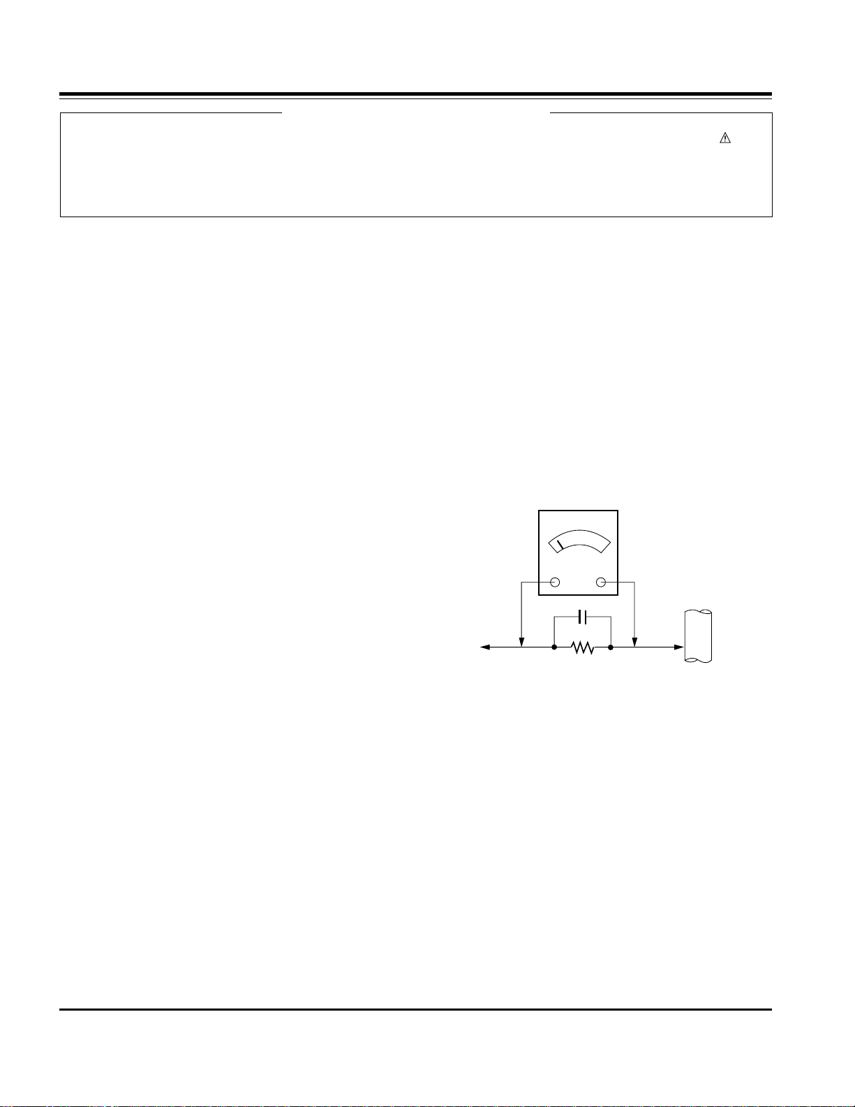
Leakage Current Hot Check (See below Figure)
Plug the AC cord directly into the AC outlet.
Do not use a line Isolation Transformer during this check.
Connect 1.5K/10watt resistor in parallel with a 0.15uF capacitor
between a known good earth ground (Water Pipe, Conduit, etc.)
and the exposed metallic parts.
Measure the AC voltage across the resistor using AC voltmeter
with 1000 ohms/volt or more sensitivity.
Reverse plug the AC cord into the AC outlet and repeat AC voltage
measurements for each exposed metallic part. Any voltage
measured must not exceed 0.75 volt RMS which is corresponds to
0.5mA.
In case any measurement is out of the limits specified, there is
possibility of shock hazard and the set must be checked and
repaired before it is returned to the customer.
Leakage Current Hot Check circuit
IMPORTANT SAFETY NOTICE
0.15uF
To Instrument's
exposed
METALLIC PARTS
AC Volt-meter
Good Earth Ground
such as WATER PIPE,
CONDUIT etc.
1.5 Kohm/10W
Page 4

- 4 -
CAUTION: Before servicing receivers covered by this service
manual and its supplements and addenda, read and follow the
SAFETY PRECAUTIONS on page 3 of this publication.
NOTE: If unforeseen circumstances create conflict between the
following servicing precautions and any of the safety precautions on
page 3 of this publication, always follow the safety precautions.
Remember: Safety First.
General Servicing Precautions
1. Always unplug the receiver AC power cord from the AC power
source before;
a. Removing or reinstalling any component, circuit board
module or any other receiver assembly.
b. Disconnecting or reconnecting any receiver electrical plug or
other electrical connection.
c. Connecting a test substitute in parallel with an electrolytic
capacitor in the receiver.
CAUTION: A wrong part substitution or incorrect polarity
installation of electrolytic capacitors may result in an
explosion hazard.
2. Test high voltage only by measuring it with an appropriate high
voltage meter or other voltage measuring device (DVM,
FETVOM, etc) equipped with a suitable high voltage probe.
Do not test high voltage by "drawing an arc".
3. Do not spray chemicals on or near this receiver or any of its
assemblies.
4. Unless specified otherwise in this service manual, clean
electrical contacts only by applying the following mixture to the
contacts with a pipe cleaner, cotton-tipped stick or comparable
non-abrasive applicator; 10% (by volume) Acetone and 90% (by
volume) isopropyl alcohol (90%-99% strength)
CAUTION: This is a flammable mixture.
Unless specified otherwise in this service manual, lubrication of
contacts in not required.
5. Do not defeat any plug/socket B+ voltage interlocks with which
receivers covered by this service manual might be equipped.
6. Do not apply AC power to this instrument and/or any of its
electrical assemblies unless all solid-state device heat sinks are
correctly installed.
7. Always connect the test receiver ground lead to the receiver
chassis ground before connecting the test receiver positive
lead.
Always remove the test receiver ground lead last.
8. Use with this receiver only the test fixtures specified in this
service manual.
CAUTION: Do not connect the test fixture ground strap to any
heat sink in this receiver.
Electrostatically Sensitive (ES) Devices
Some semiconductor (solid-state) devices can be damaged easily
by static electricity. Such components commonly are called
Electrostatically Sensitive (ES) Devices. Examples of typical ES
devices are integrated circuits and some field-effect transistors and
semiconductor "chip" components. The following techniques
should be used to help reduce the incidence of component
damage caused by static by static electricity.
1. Immediately before handling any semiconductor component or
semiconductor-equipped assembly, drain off any electrostatic
charge on your body by touching a known earth ground.
Alternatively, obtain and wear a commercially available
discharging wrist strap device, which should be removed to
prevent potential shock reasons prior to applying power to the
unit under test.
2. After removing an electrical assembly equipped with ES
devices, place the assembly on a conductive surface such as
aluminum foil, to prevent electrostatic charge buildup or
exposure of the assembly.
3. Use only a grounded-tip soldering iron to solder or unsolder ES
devices.
4. Use only an anti-static type solder removal device. Some solder
removal devices not classified as "anti-static" can generate
electrical charges sufficient to damage ES devices.
5. Do not use freon-propelled chemicals. These can generate
electrical charges sufficient to damage ES devices.
6. Do not remove a replacement ES device from its protective
package until immediately before you are ready to install it.
(Most replacement ES devices are packaged with leads
electrically shorted together by conductive foam, aluminum foil
or comparable conductive material).
7. Immediately before removing the protective material from the
leads of a replacement ES device, touch the protective material
to the chassis or circuit assembly into which the device will be
installed.
CAUTION: Be sure no power is applied to the chassis or circuit,
and observe all other safety precautions.
8. Minimize bodily motions when handling unpackaged
replacement ES devices. (Otherwise harmless motion such as
the brushing together of your clothes fabric or the lifting of your
foot from a carpeted floor can generate static electricity
sufficient to damage an ES device.)
General Soldering Guidelines
1. Use a grounded-tip, low-wattage soldering iron and appropriate
tip size and shape that will maintain tip temperature within the
range or 500
o
F to 600oF.
2. Use an appropriate gauge of RMA resin-core solder composed
of 60 parts tin/40 parts lead.
3. Keep the soldering iron tip clean and well tinned.
4. Thoroughly clean the surfaces to be soldered. Use a mall wirebristle (0.5 inch, or 1.25cm) brush with a metal handle.
Do not use freon-propelled spray-on cleaners.
5. Use the following unsoldering technique
a. Allow the soldering iron tip to reach normal temperature.
(500
o
F to 600oF)
b. Heat the component lead until the solder melts.
c. Quickly draw the melted solder with an anti-static, suction-
type solder removal device or with solder braid.
CAUTION: Work quickly to avoid overheating the
circuitboard printed foil.
6. Use the following soldering technique.
a. Allow the soldering iron tip to reach a normal temperature
(500
o
F to 600oF)
b. First, hold the soldering iron tip and solder the strand against
the component lead until the solder melts.
c. Quickly move the soldering iron tip to the junction of the
component lead and the printed circuit foil, and hold it there
only until the solder flows onto and around both the
component lead and the foil.
CAUTION: Work quickly to avoid overheating the circuit
board printed foil.
d. Closely inspect the solder area and remove any excess or
splashed solder with a small wire-bristle brush.
SERVICING PRECAUTIONS
Page 5

- 5 -
IC Remove/Replacement
Some chassis circuit boards have slotted holes (oblong) through
which the IC leads are inserted and then bent flat against the
circuit foil. When holes are the slotted type, the following technique
should be used to remove and replace the IC. When working with
boards using the familiar round hole, use the standard technique
as outlined in paragraphs 5 and 6 above.
Removal
1. Desolder and straighten each IC lead in one operation by gently
prying up on the lead with the soldering iron tip as the solder
melts.
2. Draw away the melted solder with an anti-static suction-type
solder removal device (or with solder braid) before removing the
IC.
Replacement
1. Carefully insert the replacement IC in the circuit board.
2. Carefully bend each IC lead against the circuit foil pad and
solder it.
3. Clean the soldered areas with a small wire-bristle brush.
(It is not necessary to reapply acrylic coating to the areas).
"Small-Signal" Discrete Transistor
Removal/Replacement
1. Remove the defective transistor by clipping its leads as close as
possible to the component body.
2. Bend into a "U" shape the end of each of three leads remaining
on the circuit board.
3. Bend into a "U" shape the replacement transistor leads.
4. Connect the replacement transistor leads to the corresponding
leads extending from the circuit board and crimp the "U" with
long nose pliers to insure metal to metal contact then solder
each connection.
Power Output, Transistor Device
Removal/Replacement
1. Heat and remove all solder from around the transistor leads.
2. Remove the heat sink mounting screw (if so equipped).
3. Carefully remove the transistor from the heat sink of the circuit
board.
4. Insert new transistor in the circuit board.
5. Solder each transistor lead, and clip off excess lead.
6. Replace heat sink.
Diode Removal/Replacement
1. Remove defective diode by clipping its leads as close as
possible to diode body.
2. Bend the two remaining leads perpendicular y to the circuit
board.
3. Observing diode polarity, wrap each lead of the new diode
around the corresponding lead on the circuit board.
4. Securely crimp each connection and solder it.
5. Inspect (on the circuit board copper side) the solder joints of
the two "original" leads. If they are not shiny, reheat them and if
necessary, apply additional solder.
Fuse and Conventional Resistor
Removal/Replacement
1. Clip each fuse or resistor lead at top of the circuit board hollow
stake.
2. Securely crimp the leads of replacement component around
notch at stake top.
3. Solder the connections.
CAUTION: Maintain original spacing between the replaced
component and adjacent components and the circuit board to
prevent excessive component temperatures.
Circuit Board Foil Repair
Excessive heat applied to the copper foil of any printed circuit
board will weaken the adhesive that bonds the foil to the circuit
board causing the foil to separate from or "lift-off" the board. The
following guidelines and procedures should be followed whenever
this condition is encountered.
At IC Connections
To repair a defective copper pattern at IC connections use the
following procedure to install a jumper wire on the copper pattern
side of the circuit board. (Use this technique only on IC
connections).
1. Carefully remove the damaged copper pattern with a sharp
knife. (Remove only as much copper as absolutely necessary).
2. carefully scratch away the solder resist and acrylic coating (if
used) from the end of the remaining copper pattern.
3. Bend a small "U" in one end of a small gauge jumper wire and
carefully crimp it around the IC pin. Solder the IC connection.
4. Route the jumper wire along the path of the out-away copper
pattern and let it overlap the previously scraped end of the good
copper pattern. Solder the overlapped area and clip off any
excess jumper wire.
At Other Connections
Use the following technique to repair the defective copper pattern
at connections other than IC Pins. This technique involves the
installation of a jumper wire on the component side of the circuit
board.
1. Remove the defective copper pattern with a sharp knife.
Remove at least 1/4 inch of copper, to ensure that a hazardous
condition will not exist if the jumper wire opens.
2. Trace along the copper pattern from both sides of the pattern
break and locate the nearest component that is directly
connected to the affected copper pattern.
3. Connect insulated 20-gauge jumper wire from the lead of the
nearest component on one side of the pattern break to the lead
of the nearest component on the other side.
Carefully crimp and solder the connections.
CAUTION: Be sure the insulated jumper wire is dressed so the
it does not touch components or sharp edges.
Page 6
- 6 -
SPECIFICATION
NOTE : Specifications and others are subject to change without notice for improvement
.
1. Application range
1.1 This spec sheet is applied all of the 32" LCD TV with
AL-05PA chassis.
1.2 Not included spec and each product spec in this spec
sheet apply correspondingly to the following each country
standard and requirement of Buye
2. Specification
Each part is tested as below without special appointment.
A. Temperature : 20 ± 5°C
B. Relative Humidity : 65 ± 10%
C. Power Voltage : Standard input voltage
(110~240V@ 50/60Hz)
* Standard Voltage of each product is marked by models
D. Specification and performance of each parts are followed
each drawing and specification by part number in
accordance with BOM.
E. The receiver must be operated for about 20 minutes prior
to the adjustment.
3. Test method
3.1 Performance : LGE TV test method followed.
3.2 Demanded other specification.
EMC : CISPR 13 specification
SAFETY : CB Specification
4. General Specification
No Item Specification Remark
1. Broadcasting System PAL-B/G, DTV : DVB-T
2. Available Channel 1) VHF : 02~13
2) UHF : 14~69
3) CATV : 01~125
4) DTV : 06~12, 27~69
3 Tuner IF 1) PAL : 38.90MHz
2) DVB-T : 36.167MHz
4. Input Voltage 1) AC 240V, 50Hz
5. Aspect Ratio 16:9(Wide)
6. LCD Module LC320W01-A6K6 (1366 x 768) LPL
7. Operating Environment 1) Temp : 0 ~ 40 deg
2) Humidity : 10 ~ 80 %
8. Storage Environment 1)Temp : -20 ~ 50 deg
2) Humidity : 10 ~ 90 %
Page 7

- 7 -
5. Chroma & Brightness
6. Power
No Item Min Typ Max Unit Remark
1. AC Power Operating Voltage 90 264 V
2. DC Voltage, LCD Panel Drive 11.4 12.0 12.6 V
3. DC Voltage, Inverter 22.8 24.0 25.2 V
4. DC Voltage, Sound AMP 17.4 18.0 18.6 V
5. DC Voltage, Stand By 5.6 6.0 6.4 V
6. DC Voltage, Scaler(HD2) 3.1 3.3 3.5 V
7. DC Voltage, Scaler(HD2) 1.6 1.8 1.9
8. DC Voltage, ADC 3.1 3.3 3.5 V AD9883
9. DC Voltage, VCD 5 V 4.7 5 5.3 V
10. DC Voltage, VCD 3.3V 3.1 3.3 3.5 V
11. DC Voltage, Micom 4.7 5 5.3 V
12. DC Voltage, Tuner 4.75 5.00 5.25 V
DC Voltage, Tuner 31.5 33.0 34.5 V
13. DC Voltage,Video decoder IO 3.00 3.30 3.60 V
14. DC Voltage,Video decoder Core 1.35 1.50 1.65 V
15. DC Voltage, CPLD 3.00 3.30 3.60 V XC95288
16. Audio Amp, PVDD 16.20 18.00 19.80 V TAS5122
17. Audio Amp, DVDD 3.00 3.30 3.60 V TAS5122
18 PWM Modulator IO 3.00 3.30 3.60 V NSP-6241B
19 PWM Modulator Core 2.30 2.50 2.70 V NSP-6241B
No Item Min Typ Max Unit Remark
1. Brightness 300 450 cd/m
2
2. Contrast Ratio 500:1 600:1
3. Luminance Variation 1.3 %
4. Viewing Angle(Left, Right, Up, Down) 85 88 Degree
5 Color coordinate RED X Typ 0.640 Typ
Y -0.03 0.343 +0.03
GREEN X 0.280
Y 0.605
BLUE X 0.145
Y 0.065
WHITE X 0.285
(Standard) Y 0.293
6 Color Temperature Medium 8,800 9,300 9,800 OK <Test Signal>
Cool 11,000 12,000 13,000 OK Video input, 85%
Warm 6,000 6,500 7,000 OK
Full white pattern, 5MOCD
Page 8

- 8 -
7. Component Video Input (Y, PB, PR)
8. RGB, HDMI/DVI input (DTV / PC)
No Resolution H-freq(kHz) V-freq.(kHz) Pixel clock Proposed
1. 720x576 15.625 50
2. 720x576 31.25 50
3. 640x480 15.73 59.94/60
4. 704x480 31.47 59.94/60
5. 1280x720(50/60) 37.5/45.0 50/59.94/60
6. 1920x1080(50/60) 28.125/33.75 50/59.94/60.0
No Resolution H-freq(kHz) V-freq.(kHz) Pixel clock Proposed
DTV
1. 720x576 31.25 50 EDTV576p
2. 704x480 31.47 59.94 EDTV 480p
3. 1280x720(50/60) 37.5/45.0 50/59.94/60 HDTV 720p
4. 1920x1080(50/60) 28.125/33.75 50/59.94/60.0 HDTV 1080i
PC
1. 640x350 31.468 70.09 25.17 EGA
2. 640x480 31.469 59.94 25.17 VESA(VGA)
3. 640*480 37.861 72.80 31.50 VESA(VGA)
4. 640x480 37.500 75.00 31.50 VESA(VGA)
5. 800x600 35.156 56.25 36.00 VESA(SVGA)
6. 800x600 37.879 60.31 40.00 VESA(SVGA)
7. 800x600 48.077 72.18 50.00 VESA(SVGA)
8. 800x*600 46.875 75.00 49.50 VESA(SVGA)
9. 1024x768 48.363 60.00 65.00 VESA(XGA)
10. 1024x768 56.476 70.06 75.00 VESA(XGA)
11. 1024x768 60.023 75.02 78.75 VESA(XGA)
Page 9

- 9 -
No Item Min Typ Max Unit Remark
1 Active Screen Size 800.4(diagonal) mm 31.51 inches
2 Outline Dimension 760(H) x 450(V) x 48(D) mm Typ.
3 Pixel Pitch 170.25 x 510.75 x RGB
4 Pixel Format 1366(H)x768(V) RGB stripe arrangement
5 Color Depth 8bit 16.7 Mbit
6 Luminance ,White 500 cd/m2 Center 1 point
7 Viewing Angle (CR>10) R/L 176(Typ),U/P 176(Typ) degree
8 Power Consumption 89.5 Watt Typ.
9 Weight 7.2 kg
10 Display Operating Mode Transmissive mode ,normally black
11 Surface Treatment Hard coating (3H), Anti-glare treatment
12 Altitude Operating 0 - 14,000 feet 4,267.2 m
Storage/Shipment 0 - 40,000 feet 12,192.0 m
13 Lamp Life Time 50,000 (min.) Hrs 25±2°C
9. General specifications(module)
9-1. Electro Optical Characteristic Specifications(module standard)
No Item Min Typ Max Unit Remark
1 Contrast Ratio 800 1,200 It measured at center point
2 Surface Luminance, White 400 600 Cd/m
2
Full white
3 Luminance Variation 1.3 (
white/5P)
4 Response Time Tr (Rising time) 12 msec
5 Color coordinate RED X 0.640 Full Pattern
Y 0.343
GREEN X Typ 0.280 Typ
Y -0.03 0.605 +0.03
BLUE X 0.145
Y 0.065
WHITE X 0.285
Y 0.293
6 Viewing Angle (CR>10) X axis right(
=0) 85 88
degree
X axis left(
=180) 85 88
Yaxis up (
=90) 85 88
Z axis down(
=270) 85 88
Page 10

- 10 -
10. Set factoring Condition
No Item Value Remark
1 Power Off
2 CH Memory Analog C0,C5,C6,S11,S27,C35,C52,C68
Digital C43
3 Picture PSM Dynamic
Contrast 100
Brightness 55
Color 60
Sharpness 60
Tint (Not available)
Color temperature Medium
4 Audio SSM Standard
AVL Off
Balance 0
Treble 50
Bass 50
Front surround Off
TV speaker On
BBE Off
5 Time Auto clock On Manual Clock Enable
Off timer Off
On timer Off
Sleep timer Off
Auto sleep Off
6 Special Main input Digital
Sub input Analogue
Sub title Off
Child lock Off
ARC 16:9
Cinema Off
7 LOCK Lock System Off
Block Program All programs unblocked
Parental Guide All Grade unblocked
Aux.Block All Source unblocked
8 RGB Initial DTV
9 PIP Position Right Lower
10 Volume 30
11 Favorite No Program set
Page 11
- 11 -
1. Application Object
This document is applied to 32" LCD TV which is
manufactured in Monitor Factory or is produced on the basis
of this data.
2. Notes
(1) Because this is not a hot chassis, it is not necessary to use
an isolation transformer. However, the use of isolation
transformer will help protect test equipment.
(2) Adjustments must be done in the correct order.
(3) The adjustments must be performed in the circumstance of
25±5°C of temperature and 65±10% of relative humidity if
there is no specific designation.
(4) The input voltage of the receiver be must kept 220V, 60Hz
when adjusting.
(5) The receiver must be operational for about 15 minutes
prior to the adjustments.
After receiving 100% white pattern, the receiver must be
operate prior to adjustment.(Or white condition in HEATRUN mode)
Enter into HEAT-RUN MODE
- Press the POWER ON KEY on R/C for adjustment.
OSD display and screen display 100% full WHITE
PATTERN.
[ Set is activated HEAT-RUN without signal generator in
this mode.
If you turn on a still screen more than 20 minutes (Especially
Digital pattern, Cross Hatch Pattern), an afterimage may occur
in the black level part of the screen.
3. EDID
(The extended display Identification data)
/ DDC(Display Data Channel) Download
This is the function that enables “Plug and Play".
3-1. Required Test Equipment
1) PC, Jig for adjusting DDC (PC serial to D-sub.
Connection equipment)
2) DVI to HDMI Connector
3-2. Composition of Device
3-3. EDID DATA
- Download only EDID for HDMI.
- Download only EDID for RGB.
ADJUSTMENT INSTRUCTION
Each PCB Assy must be checked by Check JIG Set before
assembly. (Especially, be careful Power PCB Assy which can
cause Damage to the LCD Module.)
00 01 02 03 04 05 06 07 08 09 0A 0B 0C 0D 0E 0F
00 00 FF FF FF FF FF FF 00 1E 6D 00 00 01 01 01 01
10 00 0F 01 03 80 46 27 78 0A 36 E9 A3 56 49 9B 25
20 11 48 4B 4F EE 80 31 4F 45 4F 61 4F 01 01 01 01
30 01 01 01 01 01 01 64 19 00 40 41 00 26 30 18 88
40 36 00 BA 88 21 00 00 18 00 00 00 FD 00 38 4B 1E
50 3D 08 00 0A 20 20 20 20 20 20 00 00 00 FC 00 33
60 32 4C 58 32 44 2D 41 41 20 20 20 20 00 00 00 00
70 00 00 00 00 00 00 00 00 00 00 00 00 00 00 01 48
80 02 03 1A 72 23 15 07 50 47 85 01 04 14 13 12 00
90 83 0F 00 00 65 03 0C 00 10 00 01 1D 80 D0 72 1C
A0 16 20 10 2C 25 80 C4 8E 21 00 00 9E 01 1D 80 18
B0 71 1C 16 20 58 2C 25 00 C4 8E 21 00 00 9E 01 1D
C0 00 BC 52 D0 1E 20 B8 28 55 40 C4 8E 21 00 00 1E
D0 01 1D 00 72 51 D0 1E 20 6E 28 55 00 C4 8E 21 00
E0 00 1E 8C 0A D0 90 20 40 31 20 0C 40 55 00 C4 8E
F0 21 00 00 18 00 00 00 00 00 00 00 00 00 00 00
EB
00 01 02 03 04 05 06 07 08 09 0A 0B 0C 0D 0E 0F
00 00 FF FF FF FF FF FF 00 1E 6D 5D 46 01 01 01 01
10 07 0F 01 03 68 46 27 96 0A FB 2C A3 57 47 9A 25
20 10 48 4B AF CE 00 31 4F 45 4F 61 4F 01 01 01 01
30 01 01 01 01 01 01 64 19 00 40 41 00 26 30 18 88
40 36 00 BC 88 21 00 00 18 00 00 00 FD 00 38 4B 1F
50 3D 08 00 0A 20 20 20 20 20 20 00 00 00 FC 00 33
60 32 4C 58 32 44 2D 41 41 0A 20 20 20 00 00 00 00
70 00 00 00 00 00 00 00 00 00 00 00 00 00 00 00 48
Page 12

- 12 -
3-4. EDID S/W Execution and Setting
1) Connect the Set, EDID Download Jig, PC & Cable. And
Execute the S/W : EDID TESTER Ver,2.5
2) Set up S/W option
Repeat Number : 3
Device Address : A0
PageByte : 8
3-5. Sequence of Adjustment
1) Init the data
2) Load the EDID data.(Open File)
[Digital(HDMI) : Checksum(5750)]
3) Set the S/W as below.
4) Push the “Write Data & Verify”button. And input the data.
5) If the writing is finished, you will see the “OK” message.
4. AD9883A-Set Adjustment
4-1. Synopsis
AD9883A-Set adjustment to set the black level and the Gain
of optimum with an automatic movement from the analog =>
digital converter.
4-2. Test Equipment
Service R/C, MSPG925 Series Pattern Generator (720P 60Hz
Color Bar Pattern output will be possible and the output level
will accurately have to be revised with 0.7±0.1Vp-p)
4-3. Adjustment
(1) Input the color Bar Pattern of the 720P 60Hz Mode what is
supportable to Component2 or RGB-DTV INPUT and the
select the Input Mode as Component2.
(2) After receiving signal for at least 1 second, press the ADJ
Key on the Service R/C to enter the ‘Ez - Adjust’ and then
select the ‘1. AD9883A-Set’.
Pressing the Vol + Key to adjust with automatic movement.
(3) If Component adjustment is completed normality,
'Component Adjustment OK' is displayed and if RGB
adjustment is completed normality, 'RGB Adjustment OK' is
displayed. If the adjustment has errors, 'AD9883A-Failed!
Try Again' is displayed.
(4) Readjust after confirming the case Pattern or adjustment
condition where the adjustment errors.
(5) After adjustment is complete, exit the adjustment mode by
pressing the ADJ KEY.
<Fig. 2> Adjustment Pattern : 720P 60Hz Color Bar Pattern
Page 13
- 13 -
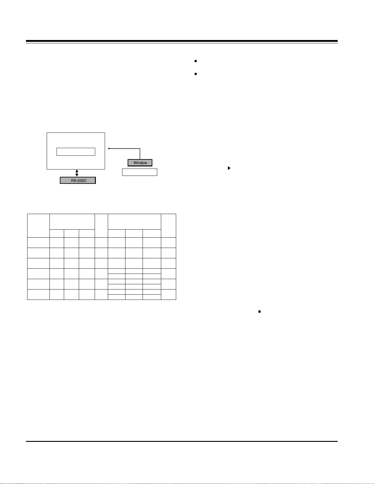
5. Adjustment of White Balance
5-1. Required Equipment
(1) Color analyzer (CA-110 or similar product)
(2) Automatic adjustor (with automatic adjustment hour
necessity and the RS-232C communication being possible)
(3) AV Pattern Generator
5-2. Connection Diagram of Equipment
for Measuring (Automatic Adjustment)
RS-232C Command (Automatic Adjustment)
5-3. Adjustment of White Balance(manual)
Operate the Zero-calibration of the CA-110, then attach
sensor to PDP module surface when you adjust.
Manual adjustment is also possible by the following
sequence.
(1) Enter ‘3.White-Pattern’ by pressing ADJ KEY on the
Service Remote Control.
(2) Select "Test Pattern White" using Vol +/- Key and Execute
HEAT RUN at least 15 minutes.
(3) Receive the HDMI/DVI 720p 60Hz, Full size, 216 Gray
window pattern signal from AV Pattern Generator.
Input mode : HDMI/DVI
Baud rate = 115200bps
(4) Select the condition of screen Adjustment as ‘Dynamic’.
(5) After attaching sensor to center of screen, select ‘2. White-
Balance’ in ‘Ez - Adjust’ by pressing the ADJ KEY on the
Service R/C. Then enter adjustment mode by pressing the
Right KEY ( ) .
a. In case color temperature is Cool.
B Gain = 192(lock)
R-Offset:64, G-Offset:64, B-Offset:64
Adjust the High Light by using R Gain/ G Gain.
b. In case color temperature is Medium
R Gain = 64(lock)
R-Offset:64, G-Offset:64, B-Offset:64
Adjust the High Light by using G Gain/ R Gain-37"
c. In case color temperature is Warm
R Gain = 192 (lock)
R-Offset:64, G-Offset:64, B-Offset:64
Adjust the High Light by using G Gain/ B Gain.
(6) Adjust using Volume +/- KEY.
luminosity value : High Level : 216gray
a. Cool : X=0.274±0.002, Y=0.274±0.002
Color temperature : 12000°K±1000°K, dUV=-3dUV
b. Medium : X=0.287±0.002, Y=0.289±0.002
Color temperature : 9300°K±1000°K, dUV=-3dUV
c. Warm : X=0.315±0.002, Y=0.316±0.002
Color temperature : 6500°K±1000°K, dUV=-3dUV
(7) After adjustment is complete, move to Ez - Adjust screen
by pressing the ENTER(
) KEY. Then exit the adjustment
mode by press ADJ KEY.
R Gain
G Gain
B Gain
R Offset
G Offset
B Offset
00
00
00
00
00
00
ff
ff
ff
7f
7f
7f
Jg
Jh
Ji
Ja
Jb
Jc
Jd
Je
Jf
C0
C0
C0
C0
C0
C0
C0
C0
C0
RS-232C Command
[CMD ID DATA]
Cool
Mid
Warm
Cool Mid
Warm
MIN
CENTER
(DEFAULT)(Hex)
MAX
<Fig. 3> Connection Diagram of Automatic Adjustment
40
40
40
40
40
40
40
40
40
40
40
40
40
40
40
40
40
40
216 FULL WHITE
COLOR
ANALYZER
TYPE; CA-110
HDMI signal input
PDP MONITOR
MSPG-925 Series
Page 14
- 14 -
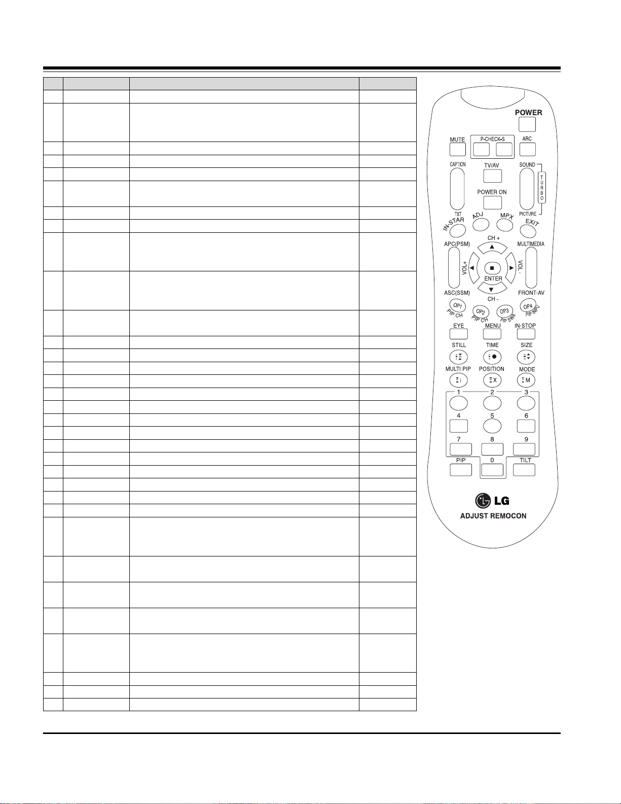
SVC REMOCON
NO. KEY FUNTION REMARK
1 POWER To turn the TV on or off
2 POWER ON
To turn the TV on automatically if the power is supplied to the TV.
(Use the POWER key to deactivate)
: It should be deactivated when delivered.
3 MUTE To activate the mute function.
4 P-CHECK To check TV screen image easily. Shortcut keys
5 S-CHECK To check TV screen sound easily Shortcut keys
6 ARC To select size of the main screen Shortcut keys
(Auto, 4:3, 16:9, 14:3, Zoom, Cinema Zoom)
7 TXT To toggle on/off the teletext mode
8 TV/AV To select an external input for the TV screen
9 IN-START To enter adjustment mode when manufacturing the TV sets.
Use the AV key to
enter the screen W/B
adjustment mode.
10 ADJ To enter into the adjustment mode.
To adjust horizontal To enter into the adjustment mode.
To adjust horizontal
11 MPX To select the multiple sound mode
(Mono, Stereo or MPEG, BOLBY, Digital)
12 EXIT To release the adjustment mode
13 APC(PSM)
To easily adjust the screen according to surrounding brightness
14 ASC(SSM) To easily adjust sound according to the program type
15 MULTIMIDIA To check component input(+RGB, HDMI/DVI) Shortcut keys
16 FRONT-AV To check the front HDMI Shortcut keys
17 CH±
To move channel up/down or to select a functiondisplayed on the screen.
18 VOL± To adjust the volume or accurately control a specific function.
19 ENTER To set a specific function or complete setting.
20 PIP CH-(OP1) To use as a red key in the teletext mode
21 PIP CH+(OP2) To use as a green key in the teletext mode
22 PIP SWAP(OP3) To use as a yellow key in the teletext mode
23 PIP INPUT(OP4) To use as a blue key in the teletext mode
24 MENU
To select the functions such as video, voice, function or channel.
25 IN-STOP
To set the delivery condition status after manufacturing the TV set.
26 STILL To halt the main screen in the normal mode,
or the sub screen at the PIP screen.
Used as a hold key in the teletext mode (Page updating is stopped.)
27 TIME Displays the teletext time in the normal mode
Enables to select the sub code in the teletext mode
28 SIZE Used as the size key in the PIP screen in the normal mode
Used as the size key in the teletext mode
29 MULTI PIP Used as the index key in the teletext mode
(Top index will be displayed if it is the top text.)
30 POSITION To select the position of the PIP screen in the normal mode
Used as the update key in the teletext mode
(Text will be displayed if the current page is updated.)
31 MODE Used as Mode in the teletext mode
32 PIP To select the simultaneous screen
33 0~9 To manually select the channel.
Page 15
- 15 -
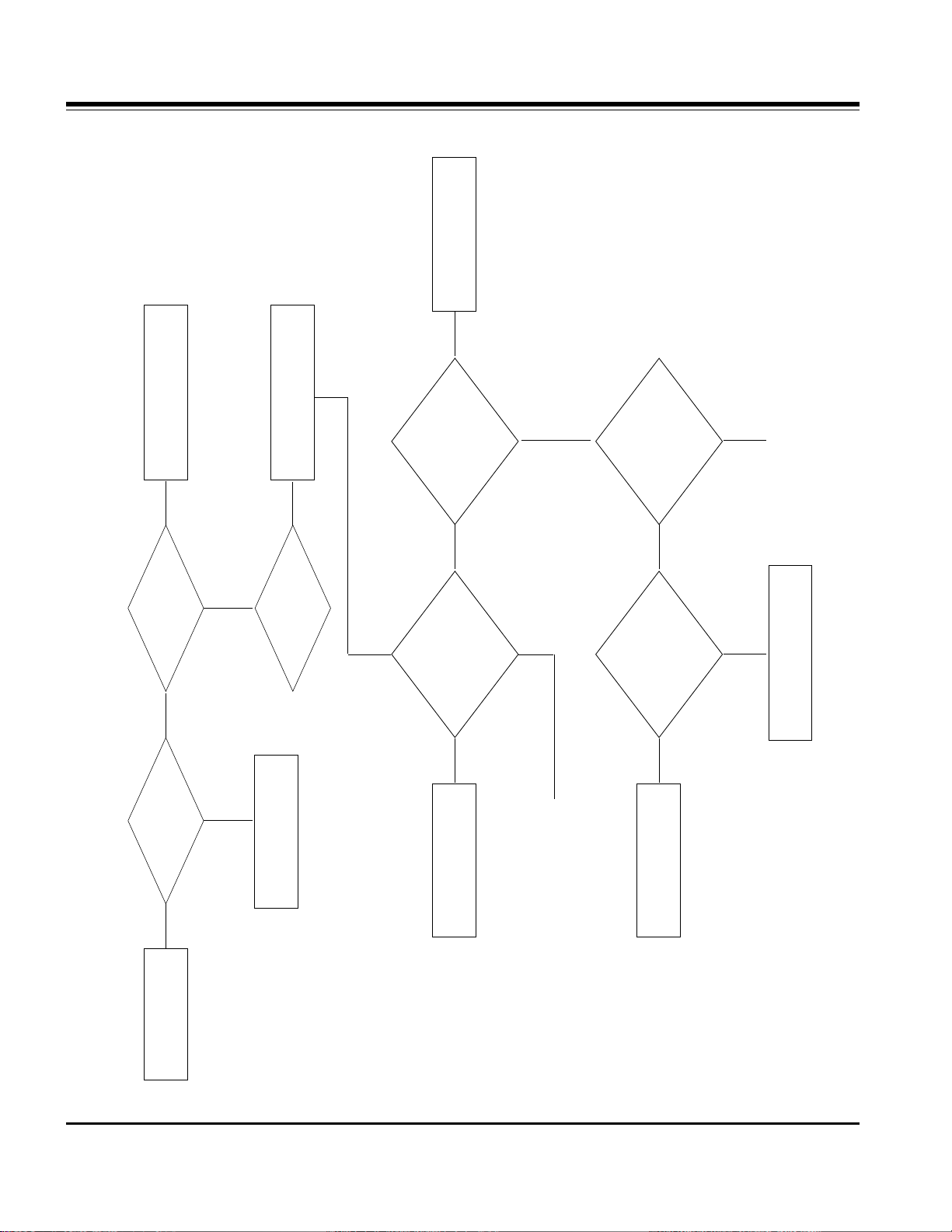
TROUBLESHOOTING
No image
Attach the input cable(s)
Push the POWER ON key
Is the Set ON?
Is the input cable
attached?
Component / S-Video
Replace SideAV boardCorrect them
What is
the input signal
mode?
Check the
Input Y, Cb, Cr
At the pin no.5,7,9 of
IC-AN15865 on
Jack board
Check the
Condition of all
Connectors, wafers, I2C
In component
Signal flow
Power Error
Replace IC1 AN15865
To sheet 20
To sheet 21
Yes
NO Yes
FAIL PASS
(component)
PASS
(S-Video)
FAIL
FAIL
PASS PASS
PASS
FAIL
NO
Check the
output YUV at
R 418, 415, 412
respectively
Check 9V
Across L401and
5V across L404
and L402
Page 16
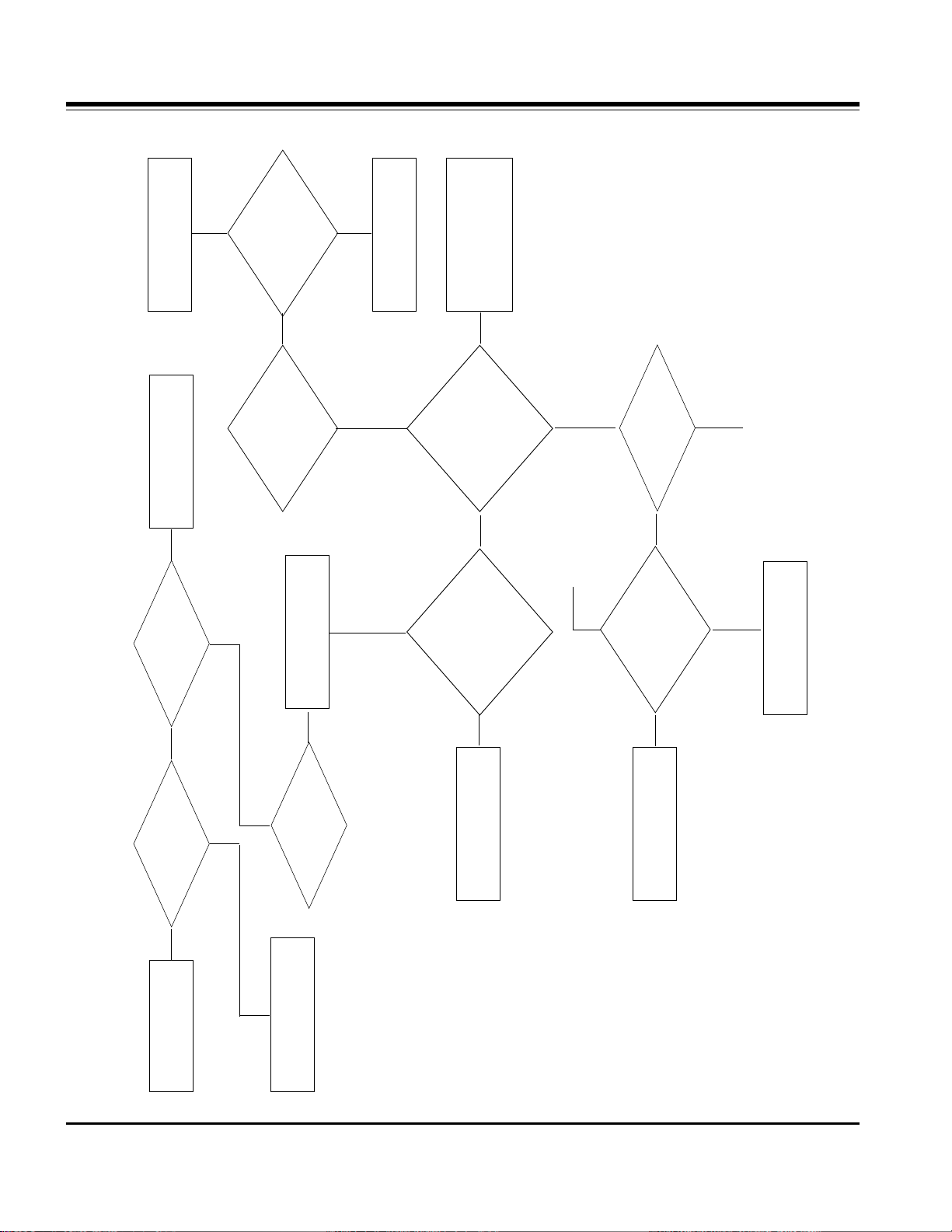
- 16 -
No image
Power Error
Attach the input cable(s)
RF/AV/IDTV input
Push the POWER ON key
Correct them
Replace IC1 AN15865
Check Tuner, SCART1/2
Front AV or Digital board
Accordingly w.r.t the Mode.
Is the
Set ON?
Power Error
Replace IC1 AN15865
Is the input cable
attached?
What is
the input signal
mode?
Check main
CVBS at R303
Check
Secondary CVBS
at R434 (for PiP)
Check 9V
Across L401and
at pin 3 of IC100
5V across
L404 , L402
Check 9V
Across L401and
at pin 3 of IC100
5V across
L404,L402
Check the
input video signal
at pin 48, 50, 52, 54, 60
of AN15865 For RF,
AV1/2/3, IDTV
Resp.
Check the
Condition of all
Connectors, wafers, I2C
In corresponding
Signal flow
Yes
NO
Yes
FAIL
PASS
FAIL
FAIL
PASS
PASS
PASS
FAIL
FAIL
FAIL
PASS
PASS
NO
To sheet 21
From sheet 22
Page 17
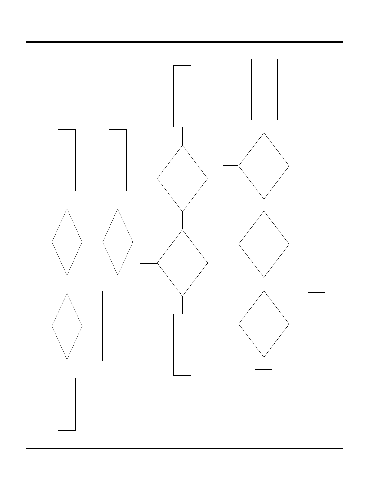
- 17 -
No image
Attach the input cable(s)
Push the POWER ON key
Is theSet ON?
Is the input cable
attached?
HDMI / DVI DTV
Replace IC accordingly
Correct them
What is
the input signal
mode?
Check the
Corresponding EDID
Storage memory (I.e.,
IC202 for DVI and
IC203 for HDMI)
Check the
Condition of all
Connectors, wafers, I2C
In corresponding
Signal flow
Power
Error
Replace IC1 AN15865
To sheet 21
Yes
Yes Yes
FAIL
FAILFAIL
PASS
PASS
PASS
PASSPASS
FAIL
FAIL
Check the interfacing ckt
Of corresponding mode
On jack board
NO
Check the
input TMDS signal
at pins 39-52 for
DVI and 58-71 for
HDMI of IC601
SiI9021
Check 24
Bit RGB output
Across AR 601-606
Check 3.3V at
L601-605 and
1.8V at pin 2 of
IC602
Page 18

- 18 -
No image
Attach input cable or
memory card
Push the POWER ON key
Is the Set ON?
Is the input cable
attached?
DVI PC / X-Studio
Check the interfacing
circuit At the jack
board or replace X-studio
Board accordingly
Correct them
What is
the input signal
mode?
Check the
i/p RGB/HV signal
At the pin no.72-76 for
X-studio and 1-2,78-80
For PC, of
AN15865
Check the
Condition of all
Connectors,wafers,I2C
and slots In corres
Ponding Signal
flow
Power Error
Replace IC1 AN15865
To sheet 20
Yes
NO Yes
FAIL PASS
FAIL FAIL
PASS
PASS
PASS
FAIL
NO
Check the
output YUV at
R 418, 415, 412
respectively
Check 9V
Across L401and
5V across L404
and L402
Page 19
- 19 -
Check the
24 bit RGB signal
output of ADC(X98014)
across RA500-501
Check the
3.3V supply volt
across L503, L504
And clock frequency
at pin 39,40
of ADC
From sheet 19
From sheet 16
To sheet 21
(DVI PC / X-Studio)
To sheet 21
(component)
Power Error
Replace ADC
PASS
PASS
PASS
FAIL
FAIL
Page 20
- 20 -
check the
output of VSP at.
10,15,16,18,20,21,22
30,31,32 pin
Check the
supply Vcc 3.3V
across L6,7 and 1.8V at pin 2
of IC11,12 and crystal
Frequency at
Pin 69,70
Check the
output of Froudja.
at pin 148-155,130-137 for
Y/C signal and clk,
VS,Hs at RF21-23
check the
RGB output of
PW181 across RAS
10-15 and sync and clk
Signal across RS
45-48
check the
supply 3.3V at LS
4, 2.5V at LS3 and 1.5V
at LS6 and LS9 and
Crystal freq
Check the
IEP output across
RAIP 1-6 and RIP
1,3,4,6
Check LVDS
output for PiP at pin
37,41,45,47 & for main image
at pin 48,46,42,38 of
IC902(LVDS IC).
check 3.3Vdd
and 2.5Vdd across
respectively
LIP2 and LIP1
check the
3.3Vdd across
CF12 and 1.8Vdd
across CF27,CF33 and 13.5
MHz at pin 191-192
of Froudja
Replace
Froudja
Replace
PW181
Power Error
Power Error
Replace LVDS
Replace IEP
Crystal or Power
Error
Replace VSP9437B
Crystal or Power Error
Crystal or Power Error
Check Power Levels and do
Power Troubleshooting
From sheet 20
(component)
From sheet 16
(S-Video)
From sheet 22
From shee 17
From sheet 18
From sheet 20
(DVI PC / X-Studio)
Check
Vcc_PLL 3.3V
Across L901
PASS
FAIL PASS
FAIL
FAIL
PASS
PASS
PASS
FAIL
FAIL
PASS
PASS
FAIL
PASSFAIL
FAILPASS
PASS
FAIL FAIL
Page 21
- 21 -
Check in
owners manual
whether the input
given for PiP is
supported
or not
Check the
YUV ouput across
RA18,20,22 if PiP is
digital or CVBS at R434
if PiP is RF/AV at
AN15865
Is PiP mode ON?
What is the
PIP input
Push PiP key
Change the input for PiP
Follow the corresponding
Troubleshooting
Procedure for same mode
To sheet 21
To sheet 17
NO
Not Supported
PASSFAIL
Any otherDTV/RF/AV
Supported
Yes
Page 22
- 22 -
1. RF/AV/Component/ X-Studio/PC-Audio
Check the
Condition of all
Connectors, wafers, I2C
In corresponding
Signal flow?
Check 18V
supply at pin 55and
pin 30 of
AMP
Check audio
output at MSP
across R655,656,657
And 605.
Check the
supply voltage 8V
across L601-602
Check the PC
R/L signal across
R621,630; Analog_SIF at
R602; Side R/L at R619,620;
Front R/L at R617,618 and X-Studio
R/L at R658-659 according to
The corresponding
mode
Is
Volume level
Of the set
0?
Check
3.3V supply across
L305 and 2.5V at
L304
Check the
PWM output of NSP
across R325-328
Is
Mute ON?
Is the Set ON?
Correct them
Replace NSP
Power Error
Replace
TAS5122 (amp)
Power Error
Check the
Amplifier output level
At L300-303
There may be some
error in Audio source.
Increase the VolumeTurn OFF the Mute
Push the POWER ON key
Check the interfacing ciruit
of PC audio, Analog Tuner,
Front AV board, Side AV
board or X-Studio board
accordingly w.r.t the mode.
No Audio
Replace the MSP
NO Yes Yes
NO
NO
Yes
FAIL
PASS
PASS
FAIL
FAIL
PASSPASS
PASS
FAIL
FAIL
PASS
PASS
FAIL
PASS
FAIL
FAIL
Page 23

- 23 -
2. IDTV/HDMI-Audio
Check the
Condition of all
Connectors, wafers, I2C
In corresponding
Signal flow?
Check the
input HDMI_I2S at
pin 1,3,6 and DTV_I2S
at pin 2,5,11 of
IC603
Check the
input I2S signal across
R632-634 of
MSP
Check audio
output at MSP
across R655,656,657
And 605.
Check the
supply voltage 8V
across L601-602
Is
Volume level
Of the set 0?
Is Mute ON?
Check the
PWM output of NSP
across R325-328
Check the
Amplifier output level
At L300-303
Check
3.3V supply across
L305 and 2.5V at
L304
Check 18V
supply at pin 55and
pin 30 of
AMP
Is the
Set ON?
Correct them
Replace the MSP
Power Error
Increase the Volume
Turn OFF the Mute
Power Error
Power Error
Replace NSP
Push the POWER ON key
There may be some
error in PC input.
Replace TAS5122(amp)
Check the SiI9021 or
Digital board accordingly.
No Audio
FAIL PASS PASS
FAILFAILPASS
FAIL
Check
5V at pin 16 of
IC603
Replace IC907
PASS
FAIL
PASS
PASS
FAIL
PASS
FAIL
FAIL
PASS
PASS
FAIL
PASS
PASS
PASS
FAIL
FAIL
FAIL
PASS
FAIL
Page 24

- 24 -
BLOCK DIAGRAM(Video)
Page 25

- 25 -
BLOCK DIAGRAM(Audio)
DH_LINE_SCK
DH_LINE_LRCK
DH_LINE_LRCH
*AV : LR
*Component1
CS5330A
∆LR, SPDIF (Priority)
*Component2 : LR
*RGB (PC/DTV) : LR
mode
Slave
HA_MCLK
(ADC)
Master mode
(Buffer)
MC33078
∆LR, SPDIF (Priority)
*DVI (PC/DTV)
*HDMI
HD2.3
*Dolby Digital
HB_DAC_SCK
HB_DAC_LRCK
(Buffer)
74LCX224
AH_IEC958IN (I2S)
AH_SPDIFCLK (MCLK)
mode
Master
(CPLD)
XC95288XL
SPDIF_MUX_OUT
SPDIF IN
OPTIC (DVD)
SPDIF_DVD
SPDIF_HDMI
(HDMI)
SiI9011
RXC/0/1/2C
(from CPU)
SEL_SPDIF_DVD/nDVI
SPDIF OUT
74LCX157
(Tx Buffer)
HA_IEC958OUT (SPDIF)
SPDIF IN
OPTIC (DVI)
SPDIF_DVI
(from CPU)
SEL_SPDIF_HD2_nSPDIF
I2S
CS8415A
(SPDIF Rx)
(to CPU)
(to CPU)
AC_ERROR_SPDIF
nAC_EMPH_SPDIF
(to CPU)
8415_IRQ_ERR
Slave mode
SPDIF =>
SPDIF_DVI
SPDIF_DVD
SPDIF_HDMI
(from CPU)
nCA_RST_SPDIF
DIGITAL TUNER_TP_DATA
Analog_LR
AV_LR
CXA2069
AV1
MSP4410
(AV Switch)
EPF
AV2
BA_DAC_SCK
BA_DAC_LRCK
HA_DAC_LRCH
*SIF Demod.
*Treble/bass
*Balance
*Volume
*SRS True
Comp1_LR
Comp2_LR
*BBE
Master mode
RGB_LR
PAL TUNER_SIF
MNT_LROUT
MNT
OUT
(PWM)
NSP6241B
Slave mode
I2S_MCLK
I2S_SCK
I2S_LRCK
AN_LINE_LRCH
PWM_LR
TAS5122
LC
SPK
Out
(D.Amp)
LPF
Page 26

- 26 -
WIRING DIAGRAM
1
2
1 - 6631T11023F : 31P
2 - 6631T20037D : 12P
3 - 6631T20037E : 12P
4 - 6631T25024G : 3P
5 - 6631T25024H : 4P
6 - 6631T25023H : 15P
7 - 6631T25024Z : 3P
8 - 6631T11022A : 31P
9 - 6631T25019W : 5P
10 - 6631T25023R : 13P
11 - 6631T20037H : 12P
12 - 6631T20037N : 7P
13 - 6631T20037Q : 3P
14 - 6631T11022A : 31P
15 - 6631T25020L : 13P
16 - 6631T20037H : 12P
17 - 6631T20037L : 10P
3
4
5
6
7
8
8 8
9
10
11
12
13
14
15
16
17
Page 27

- 27 -
EXPLODED VIEW
030
050
180
110
070
060
170
160
100
150
090
080
140
040
020
010
130
120
Page 28

- 28 -
EXPLODED VIEW PARTS LIST
No.
PART NO.
DESCRIPTION
3091TKE037H CABINET ASSEMBLY, 32LX2D-AA BRAND CABINET ASSY
6304FLP288A
LCD(LIQUID CRYSTAL DISPLAY), LC320W01-SL01 LG PHILPS TFT COLOR WXGA AIODC SPEC UP LEAD FREE
3809TKE030V BACK COVER ASSEMBLY, 32LX2D-AA DTV 3808TKE025 SET
3043TKK252A TILT SWIVEL ASSEMBLY, 32LX2D-UA STAND ASSY
3550TKK881C COVER, 32LX2D NO SPRAY REAR AV COVER
4951TKS222G METAL ASSEMBLY, FRAME METAL ASSY 32LX1D-NA
6400GESF01A
SPEAKER,FULLRANGE, C112A02K1450 ESTEC FULL-RANGE(GENERAL) 8OHM 10/15W .DB 110 32LG10
6871TPT303B
PWB(PCB) ASSEMBLY,POWER, DU/DN/DI-32LP10 POWER TOTAL BRAND DU(DCR) COMM - SH(D112)
33139D3012A MAIN TOTAL ASSEMBLY, 32LX2D BRAND AL-05PB
68719ST791A PWB(PCB) ASSEMBLY,SUB, SUB T.T AB 32LX2D-AA ALAULVX TUNER
4951TKK238J METAL ASSEMBLY, FRAME, REAR 32LX2D-AA
68719ST790A PWB(PCB) ASSEMBLY,SUB, SUB T.T AB 32LX2D-AA ALAULVX CONTROL KEY
68719ST789A PWB(PCB) ASSEMBLY,SUB, SUB T.T AB 32LX2D-AA ALAULVX LIGHT&IR ETC
4950TKA210A METAL, SIDE BRACKET 32LX1D LPL MODULE
33139D3011A MAIN TOTAL ASSEMBLY, 32LX2D-AA BRAND AL-05PB
68719ST788A PWB(PCB) ASSEMBLY,SUB, SUB T.T AB 32LX2D-AA ALAULVX SIDE COMP SUB TOTAL
4815TKK046J SHIELD ASSEMBLY, REAR SHIELD ASSY 32LX2D-AA
3551TKK589U COVER ASSEMBLY, DTV 32LX2D-AA REAR AV BRACKET ASSY
010
020
030
040
050
060
070
080
090
100
110
120
130
140
150
160
170
180
Page 29

- 29 -
DATE: 2005. 09. 12.
*S *AL LOC. NO. PART NO. DESCRIPTION / SPECIFICATION
C110 0CH3104K566 0.1UF 50V 10% X7R 2012 R/TP
C112 0CH3104K566 0.1UF 50V 10% X7R 2012 R/TP
C113 0CH3104K566 0.1UF 50V 10% X7R 2012 R/TP
C114 0CH3104K566 0.1UF 50V 10% X7R 2012 R/TP
C206 0CH2103K666 0.01UF 50V 20% X7R 2012 R/T
C208 0CH2103K666 0.01UF 50V 20% X7R 2012 R/T
C219 0CH5102K416 1000PF 50V 5% NP0 2012 R/TP
C220 0CH2103K666 0.01UF 50V 20% X7R 2012 R/T
C221 0CH5102K416 1000PF 50V 5% NP0 2012 R/TP
C222 0CH2103K666 0.01UF 50V 20% X7R 2012 R/T
C224 0CH5181K416 180PF 50V 5% NP0 2012 R/TP
C304 0CH2103K666 0.01UF 50V 20% X7R 2012 R/T
C310 0CH3104K566 0.1UF 50V 10% X7R 2012 R/TP
C311 0CH2103K666 0.01UF 50V 20% X7R 2012 R/T
C318 0CK225DFK4A "2.2UF 2012 16V 20%,-20% F(Y"
C319 0CK225DFK4A "2.2UF 2012 16V 20%,-20% F(Y"
C325 0CK225DFK4A "2.2UF 2012 16V 20%,-20% F(Y"
C327 0CK225DFK4A "2.2UF 2012 16V 20%,-20% F(Y"
C410 0CH5680K416 68PF 50V 5% NP0 2012 R/TP
C411 0CH5330K416 33PF 50V 5% NP0 2012 R/TP
C412 0CH5330K416 33PF 50V 5% NP0 2012 R/TP
C420 0CH2103K666 0.01UF 50V 20% X7R 2012 R/T
C421 0CH2103K666 0.01UF 50V 20% X7R 2012 R/T
C422 0CH2103K666 0.01UF 50V 20% X7R 2012 R/T
C423 0CH2103K666 0.01UF 50V 20% X7R 2012 R/T
C424 0CH2103K666 0.01UF 50V 20% X7R 2012 R/T
C427 0CH2103K666 0.01UF 50V 20% X7R 2012 R/T
C434 0CH2103K666 0.01UF 50V 20% X7R 2012 R/T
C439 0CH2103K666 0.01UF 50V 20% X7R 2012 R/T
C440 0CH2103K666 0.01UF 50V 20% X7R 2012 R/T
C441 0CH2103K666 0.01UF 50V 20% X7R 2012 R/T
C442 0CH2103K666 0.01UF 50V 20% X7R 2012 R/T
C444 0CH2103K666 0.01UF 50V 20% X7R 2012 R/T
C501 0CH2103K666 0.01UF 50V 20% X7R 2012 R/T
C503 0CH2822K516 8200PF 50V 10% B(Y5P) 2012
C506 0CH3104K566 0.1UF 50V 10% X7R 2012 R/TP
C508 0CH2103K666 0.01UF 50V 20% X7R 2012 R/T
C512 0CH5020K116 2PF 2012 50V 0.5 PF NP0 R/T
C513 0CH5020K116 2PF 2012 50V 0.5 PF NP0 R/T
C515 0CH5560K416 56PF 50V 5% NP0 2012 R/TP
C516 0CH5560K416 56PF 50V 5% NP0 2012 R/TP
C522 0CH2103K666 0.01UF 50V 20% X7R 2012 R/T
C524 0CH5102K416 1000PF 50V 5% NP0 2012 R/TP
C527 0CH3104K566 0.1UF 50V 10% X7R 2012 R/TP
C530 0CH3104K566 0.1UF 50V 10% X7R 2012 R/TP
C537 0CH2103K666 0.01UF 50V 20% X7R 2012 R/T
C541 0CH3104K566 0.1UF 50V 10% X7R 2012 R/TP
C559 0CK225DFK4A "2.2UF 2012 16V 20%,-20% F(Y"
C570 0CH3104K566 0.1UF 50V 10% X7R 2012 R/TP
C571 0CH3104K566 0.1UF 50V 10% X7R 2012 R/TP
C572 0CH3104K566 0.1UF 50V 10% X7R 2012 R/TP
C573 0CH3104K566 0.1UF 50V 10% X7R 2012 R/TP
C574 0CH3104K566 0.1UF 50V 10% X7R 2012 R/TP
C575 0CH2103K666 0.01UF 50V 20% X7R 2012 R/T
C578 0CH3104K566 0.1UF 50V 10% X7R 2012 R/TP
C586 0CH3104K566 0.1UF 50V 10% X7R 2012 R/TP
DATE: 2005. 09. 12.
*S *AL LOC. NO. PART NO. DESCRIPTION / SPECIFICATION
C587 0CH3104K566 0.1UF 50V 10% X7R 2012 R/TP
C588 0CH3104K566 0.1UF 50V 10% X7R 2012 R/TP
C589 0CH3104K566 0.1UF 50V 10% X7R 2012 R/TP
C590 0CH2103K666 0.01UF 50V 20% X7R 2012 R/T
C591 0CH3104K566 0.1UF 50V 10% X7R 2012 R/TP
C592 0CH3104K566 0.1UF 50V 10% X7R 2012 R/TP
C593 0CH2103K666 0.01UF 50V 20% X7R 2012 R/T
C601 0CH3104K566 0.1UF 50V 10% X7R 2012 R/TP
C603 0CH3104K566 0.1UF 50V 10% X7R 2012 R/TP
C605 0CH3104K566 0.1UF 50V 10% X7R 2012 R/TP
C606 0CH2103K666 0.01UF 50V 20% X7R 2012 R/T
C608 0CH3104K566 0.1UF 50V 10% X7R 2012 R/TP
C609 0CH3104K566 0.1UF 50V 10% X7R 2012 R/TP
C610 0CH2103K666 0.01UF 50V 20% X7R 2012 R/T
C611 0CH2103K666 0.01UF 50V 20% X7R 2012 R/T
C614 0CH3104K566 0.1UF 50V 10% X7R 2012 R/TP
C615 0CH3104K566 0.1UF 50V 10% X7R 2012 R/TP
C618 0CH3104K566 0.1UF 50V 10% X7R 2012 R/TP
C619 0CH3104K566 0.1UF 50V 10% X7R 2012 R/TP
C622 0CH3104K566 0.1UF 50V 10% X7R 2012 R/TP
C623 0CH3104K566 0.1UF 50V 10% X7R 2012 R/TP
C625 0CH3104K566 0.1UF 50V 10% X7R 2012 R/TP
C627 0CH2103K666 0.01UF 50V 20% X7R 2012 R/T
C628 0CH2103K666 0.01UF 50V 20% X7R 2012 R/T
C631 0CH2103K666 0.01UF 50V 20% X7R 2012 R/T
C637 0CH3104K566 0.1UF 50V 10% X7R 2012 R/TP
C638 0CH2103K666 0.01UF 50V 20% X7R 2012 R/T
C642 0CH3104K566 0.1UF 50V 10% X7R 2012 R/TP
C643 0CH3104K566 0.1UF 50V 10% X7R 2012 R/TP
C645 0CH3104K566 0.1UF 50V 10% X7R 2012 R/TP
C653 0CH3104K566 0.1UF 50V 10% X7R 2012 R/TP
C656 0CH3104K566 0.1UF 50V 10% X7R 2012 R/TP
C662 0CH3104K566 0.1UF 50V 10% X7R 2012 R/TP
C664 0CH3104K566 0.1UF 50V 10% X7R 2012 R/TP
C667 0CH2103K666 0.01UF 50V 20% X7R 2012 R/T
C668 0CH3104K566 0.1UF 50V 10% X7R 2012 R/TP
C680 0CH3104K566 0.1UF 50V 10% X7R 2012 R/TP
C702 0CH5471K416 470PF 50V 5% NP0 2012 R/TP
C703 0CH5471K416 470PF 50V 5% NP0 2012 R/TP
C301 0CK104CK56A 0.1UF 1608 50V 10% R/TP X7R
C305 0CK104CK56A 0.1UF 1608 50V 10% R/TP X7R
C306 0CK104CK56A 0.1UF 1608 50V 10% R/TP X7R
C312 0CK104CK56A 0.1UF 1608 50V 10% R/TP X7R
C313 0CK474CH94A "0.47UF 1608 25V 80%,-20% R/"
C314 0CK474CH94A "0.47UF 1608 25V 80%,-20% R/"
C316 0CK474CH94A "0.47UF 1608 25V 80%,-20% R/"
C320 0CK104CK56A 0.1UF 1608 50V 10% R/TP X7R
C321 0CK474CH94A "0.47UF 1608 25V 80%,-20% R/"
C322 0CK104CK56A 0.1UF 1608 50V 10% R/TP X7R
C324 0CK474CH94A "0.47UF 1608 25V 80%,-20% R/"
C428 0CK103CK51A 0.01UF 1608 50V 10% R/TP B(
C430 0CK103CK51A 0.01UF 1608 50V 10% R/TP B(
C435 0CK103CK51A 0.01UF 1608 50V 10% R/TP B(
C437 0CK104CK56A 0.1UF 1608 50V 10% R/TP X7R
REPLACEMENT PARTS LIST
MAIN BOARD(Analog)
CAPACITOR
For Capacitor & Resistors, the
charactors at 2nd and 3rd digit in the
P/No. means as follows;
CC, CX, CK, CN, CH : Ceramic
CQ : Polyestor
CE : Electrolytic
CF : Fixed Film
RD : Carbon Film
RS : Metal Oxide Film
RN : Metal Film
RH : CHIP, Metal Glazed(Chip)
RR : Drawing
Page 30

- 30 -
DATE: 2005. 09. 12.
*S *AL LOC. NO. PART NO. DESCRIPTION / SPECIFICATION
C514 0CK104CK56A 0.1UF 1608 50V 10% R/TP X7R
C517 0CK474CH94A "0.47UF 1608 25V 80%,-20% R/"
C518 0CK474CH94A "0.47UF 1608 25V 80%,-20% R/"
C519 0CK474CH94A "0.47UF 1608 25V 80%,-20% R/"
C521 0CK474CH94A "0.47UF 1608 25V 80%,-20% R/"
C525 0CK102CK56A 1000PF 1608 50V 0.1 R/TP X7
C528 0CK474CH94A "0.47UF 1608 25V 80%,-20% R/"
C529 0CK222CK51A 2200PF 1608 50V 10% R/TP B(
C532 0CK474CH94A "0.47UF 1608 25V 80%,-20% R/"
C534 0CK222CK51A 2200PF 1608 50V 10% R/TP B(
C535 0CK104CK56A 0.1UF 1608 50V 10% R/TP X7R
C536 0CK222CK51A 2200PF 1608 50V 10% R/TP B(
C539 0CK222CK51A 2200PF 1608 50V 10% R/TP B(
C540 0CK103CK51A 0.01UF 1608 50V 10% R/TP B(
C542 0CK222CK51A 2200PF 1608 50V 10% R/TP B(
C546 0CK222CK51A 2200PF 1608 50V 10% R/TP B(
C547 0CK474CH94A "0.47UF 1608 25V 80%,-20% R/"
C548 0CK222CK51A 2200PF 1608 50V 10% R/TP B(
C549 0CK474CH94A "0.47UF 1608 25V 80%,-20% R/"
C550 0CK222CK51A 2200PF 1608 50V 10% R/TP B(
C553 0CK103CK51A 0.01UF 1608 50V 10% R/TP B(
C556 0CK105DK94A "1UF 2012 50V 80%,-20% R/TP"
C557 0CK104CK56A 0.1UF 1608 50V 10% R/TP X7R
C560 0CK105DK94A "1UF 2012 50V 80%,-20% R/TP"
C561 0CK104CK56A 0.1UF 1608 50V 10% R/TP X7R
C564 0CK104CK56A 0.1UF 1608 50V 10% R/TP X7R
C569 0CK104CK56A 0.1UF 1608 50V 10% R/TP X7R
C579 0CK333CK56A 33000PF 1608 50V 10% R/TP X
C580 0CK333CK56A 33000PF 1608 50V 10% R/TP X
C581 0CK333CK56A 33000PF 1608 50V 10% R/TP X
C582 0CK333CK56A 33000PF 1608 50V 10% R/TP X
C594 0CK103CK51A 0.01UF 1608 50V 10% R/TP B(
C595 0CK103CK51A 0.01UF 1608 50V 10% R/TP B(
C596 0CK103CK51A 0.01UF 1608 50V 10% R/TP B(
C626 0CK104CK56A 0.1UF 1608 50V 10% R/TP X7R
C632 0CK103CK51A 0.01UF 1608 50V 10% R/TP B(
C651 0CK104CK56A 0.1UF 1608 50V 10% R/TP X7R
C654 0CK104CK56A 0.1UF 1608 50V 10% R/TP X7R
C658 0CK104CK56A 0.1UF 1608 50V 10% R/TP X7R
C661 0CK104CK56A 0.1UF 1608 50V 10% R/TP X7R
C674 0CK103CK51A 0.01UF 1608 50V 10% R/TP B(
C675 0CK104CK56A 0.1UF 1608 50V 10% R/TP X7R
C701 0CK104CK56A 0.1UF 1608 50V 10% R/TP X7R
C101 0CH6101K416 100PF 50V 5% NP0 2012 R/TP
C104 0CH6101K416 100PF 50V 5% NP0 2012 R/TP
C115 0CH6101K416 100PF 50V 5% NP0 2012 R/TP
C116 0CH6101K416 100PF 50V 5% NP0 2012 R/TP
C223 0CH6101K416 100PF 50V 5% NP0 2012 R/TP
C323 0CH2474F566 0.47UF 16V 10% X7R 2012 R/T
C326 0CH2474F566 0.47UF 16V 10% X7R 2012 R/T
C413 0CH2474F566 0.47UF 16V 10% X7R 2012 R/T
C502 0CH2152K516 1500PF 50V 10% B(Y5P) 2012
C505 0CH2152K516 1500PF 50V 10% B(Y5P) 2012
C538 0CH2474F566 0.47UF 16V 10% X7R 2012 R/T
C543 0CC101CK41A 100PF 1608 50V 5% R/TP NP0
C554 0CC471CK41A 470PF 1608 50V 5% R/TP NP0
C583 0CE108EJK18 "1000UF KMG,RD 35V 20%,-20%"
C597 0CE108EJK18 "1000UF KMG,RD 35V 20%,-20%"
C111 0CE476SF6DC 47UF MVG 16V 20% SMD R/TP
C226 0CE227SF6DC 220UF MVG 16V 20% R/TP(SMD)
C227 0CE227SF6DC 220UF MVG 16V 20% R/TP(SMD)
C307 0CE226SF6DC 22UF MVG 16V 20% SMD R/TP
DATE: 2005. 09. 12.
*S *AL LOC. NO. PART NO. DESCRIPTION / SPECIFICATION
C308 0CE227SF6DC 220UF MVG 16V 20% R/TP(SMD)
C309 0CE476SF6DC 47UF MVG 16V 20% SMD R/TP
C414 0CE106SF6DC 10UF MVG 16V 20% R/TP(SMD)
C415 0CE106SF6DC 10UF MVG 16V 20% R/TP(SMD)
C416 0CE106SF6DC 10UF MVG 16V 20% R/TP(SMD)
C417 0CE106SF6DC 10UF MVG 16V 20% R/TP(SMD)
C418 0CE106SF6DC 10UF MVG 16V 20% R/TP(SMD)
C426 0CE106SF6DC 10UF MVG 16V 20% R/TP(SMD)
C429 0CE106SF6DC 10UF MVG 16V 20% R/TP(SMD)
C431 0CE106SF6DC 10UF MVG 16V 20% R/TP(SMD)
C432 0CE105SK6DC 1UF MVG 50V 20% SMD R/TP
C433 0CE106SF6DC 10UF MVG 16V 20% R/TP(SMD)
C436 0CE106SF6DC 10UF MVG 16V 20% R/TP(SMD)
C438 0CE476SF6DC 47UF MVG 16V 20% SMD R/TP
C443 0CE106SF6DC 10UF MVG 16V 20% R/TP(SMD)
C507 0CE476SF6DC 47UF MVG 16V 20% SMD R/TP
C511 0CE226SF6DC 22UF MVG 16V 20% SMD R/TP
C520 0CE335SK6DC 3.3UF MVG 50V 20% SMD R/TP
C531 0CE226SF6DC 22UF MVG 16V 20% SMD R/TP
C533 0CE106SF6DC 10UF MVG 16V 20% R/TP(SMD)
C544 0CE106SF6DC 10UF MVG 16V 20% R/TP(SMD)
C555 0CE335SK6DC 3.3UF MVG 50V 20% SMD R/TP
C563 0CE107SF6DC 100UF MVG 16V 20% SMD R/TP
C566 0CE106SF6DC 10UF MVG 16V 20% R/TP(SMD)
C567 0CE106SF6DC 10UF MVG 16V 20% R/TP(SMD)
C576 0CE475VK6DC 4.7UF MV 50V 20% R/TP(SMD)
C577 0CE475VK6DC 4.7UF MV 50V 20% R/TP(SMD)
C602 0CE107SF6DC 100UF MVG 16V 20% SMD R/TP
C604 0CE107SF6DC 100UF MVG 16V 20% SMD R/TP
C607 0CE107SF6DC 100UF MVG 16V 20% SMD R/TP
C612 0CE107SF6DC 100UF MVG 16V 20% SMD R/TP
C613 0CE107SF6DC 100UF MVG 16V 20% SMD R/TP
C616 0CE477SF6DC 470UF MVG 16V 20% R/TP(SMD)
C617 0CE107SF6DC 100UF MVG 16V 20% SMD R/TP
C620 0CE107SF6DC 100UF MVG 16V 20% SMD R/TP
C621 0CE227SF6DC 220UF MVG 16V 20% R/TP(SMD)
C629 0CE107SF6DC 100UF MVG 16V 20% SMD R/TP
C633 0CE107SF6DC 100UF MVG 16V 20% SMD R/TP
C635 0CE107SF6DC 100UF MVG 16V 20% SMD R/TP
C636 0CE107SF6DC 100UF MVG 16V 20% SMD R/TP
C639 0CE107SF6DC 100UF MVG 16V 20% SMD R/TP
C640 0CE476VK6DC 47UF MV 50V 20% R/TP(SMD) S
C641 0CE476VK6DC 47UF MV 50V 20% R/TP(SMD) S
C644 0CE107VH6DC 100UF MV 25V 20% R/TP(SMD)
C646 0CE107VH6DC 100UF MV 25V 20% R/TP(SMD)
C652 0CE476SF6DC 47UF MVG 16V 20% SMD R/TP
C655 0CE107SF6DC 100UF MVG 16V 20% SMD R/TP
C657 0CE107SF6DC 100UF MVG 16V 20% SMD R/TP
C659 0CE107SF6DC 100UF MVG 16V 20% SMD R/TP
C660 0CE107SF6DC 100UF MVG 16V 20% SMD R/TP
C663 0CE476SF6DC 47UF MVG 16V 20% SMD R/TP
C665 0CE476SF6DC 47UF MVG 16V 20% SMD R/TP
C666 0CE476SF6DC 47UF MVG 16V 20% SMD R/TP
C672 0CE476SF6DC 47UF MVG 16V 20% SMD R/TP
C681 0CE476WF6DC 47UF MVK 16V 20% R/TP(SMD)
C584 0CF4741L438 0.47UF D 63V 5% TP 5 M/PE N
C585 0CF4741L438 0.47UF D 63V 5% TP 5 M/PE N
ZD101 0DR050008AA SD05.TC R/TP SEMTECH SOD323
ZD102 0DR050008AA SD05.TC R/TP SEMTECH SOD323
DIODEs
Page 31

DATE: 2005. 09. 12.
*S *AL LOC. NO. PART NO. DESCRIPTION / SPECIFICATION
ZD301 0DR050008AA SD05.TC R/TP SEMTECH SOD323
ZD302 0DR050008AA SD05.TC R/TP SEMTECH SOD323
D101 0DS226009AA KDS226 TP KEC - 80V - - 4NS
D102 0DS226009AA KDS226 TP KEC - 80V - - 4NS
D103 0DS226009AA KDS226 TP KEC - 80V - - 4NS
D403 0DS226009AA KDS226 TP KEC - 80V - - 4NS
D404 0DS226009AA KDS226 TP KEC - 80V - - 4NS
D601 0DS226009AA KDS226 TP KEC - 80V - - 4NS
D602 0DS226009AA KDS226 TP KEC - 80V - - 4NS
D603 0DS226009AA KDS226 TP KEC - 80V - - 4NS
ZD108 0DZ510009EE UDZ S 5.1B TP ROHM-K SOD323
ZD109 0DZ510009EE UDZ S 5.1B TP ROHM-K SOD323
ZD303 0DZ510009EE UDZ S 5.1B TP ROHM-K SOD323
ZD304 0DZ510009EE UDZ S 5.1B TP ROHM-K SOD323
ZD501 0DZ820009AH MTZJ8.2B TP ROHM-K DO34 - 8
IC403 0IMMRMR006E "MX29LV160BTTC-70G,LF MACRON"
IC101 0IMMR00018A 24LC02BT-I/SNG(PB FREE) MIC
IC402 0IMMRHY001L "HY57V641620ETP-H,LF HYNIX 5"
IC404 0IMCRAL006A "AT24C16AN-10SU-2.7,LF ATMEL"
IC301 0ISO206900A CXA2069Q QFP64 BK I2C BUS A
IC401 0IMCRMN023A SDA6001 QH B12 MICRONAS 128
IC501 0IMCRMN028B MSP4410K MICRONAS 80P/PQFP
IC502 0IMCRNL001C "NSP-6241B,PB FREE NEOFIDELI"
IC503 0IMCRTI028C "TAS5122DCARG4,LF TEXAS INS"
IC405 0IKE702700D "KIA7027AF 3, SOT-89 TP RESE"
IC601 0IMCRFA010A "KA7809R, FAIRCHILD 2P D-PAK"
IC602 0IPRPML001A MIC39100 MICREL 3P SOT223 R
IC603 0IPMGKE030A KIA78R05F KEC 5PIN DPAK R/T
L506 6140VB0022A CPS-0810 GET 22UH 21.5TURNS
L507 6140VB0022A CPS-0810 GET 22UH 21.5TURNS
L508 6140VB0022A CPS-0810 GET 22UH 21.5TURNS
L509 6140VB0022A CPS-0810 GET 22UH 21.5TURNS
R707 6210TCE001P HB-1S2012-121JT CERATECH 20
R708 6210TCE001P HB-1S2012-121JT CERATECH 20
L600 6210TCE001P HB-1S2012-121JT CERATECH 20
L601 6210TCE001P HB-1S2012-121JT CERATECH 20
L602 6210TCE001P HB-1S2012-121JT CERATECH 20
L603 6210TCE001P HB-1S2012-121JT CERATECH 20
L206 6210VC0005A BK2125 HS 750 TAIYOYUDEN 2X
L208 6210VC0005A BK2125 HS 750 TAIYOYUDEN 2X
L209 6210VC0005A BK2125 HS 750 TAIYOYUDEN 2X
L211 6200JB8010L MLB-201209-1000L-N2 MAG LAY
L216 6200JB8010L MLB-201209-1000L-N2 MAG LAY
L217 6200JB8010L MLB-201209-1000L-N2 MAG LAY
L218 6200JB8010L MLB-201209-1000L-N2 MAG LAY
L303 6210TCE001A HB-1S2012-080JT CERATEC 201
L305 6210TCE001A HB-1S2012-080JT CERATEC 201
L307 6210TCE001A HB-1S2012-080JT CERATEC 201
L309 6210TCE001A HB-1S2012-080JT CERATEC 201
L311 6210TCE001A HB-1S2012-080JT CERATEC 201
L408 6210TCE001G HH-1M3216-501 CERATEC 3216M
L510 6200JB8010L MLB-201209-1000L-N2 MAG LAY
L511 6200JB8010L MLB-201209-1000L-N2 MAG LAY
L613 6210TCE001G HH-1M3216-501 CERATEC 3216M
L614 6210TCE001G HH-1M3216-501 CERATEC 3216M
L616 6210TCE001G HH-1M3216-501 CERATEC 3216M
DATE: 2005. 09. 12.
*S *AL LOC. NO. PART NO. DESCRIPTION / SPECIFICATION
L618 6210TCE001G HH-1M3216-501 CERATEC 3216M
L619 6210TCE001G HH-1M3216-501 CERATEC 3216M
L620 6210TCE001G HH-1M3216-501 CERATEC 3216M
L621 6210TCE001G HH-1M3216-501 CERATEC 3216M
L622 6210TCE001G HH-1M3216-501 CERATEC 3216M
L108 6210TCE001G HH-1M3216-501 CERATEC 3216M
L302 6210TCE001G HH-1M3216-501 CERATEC 3216M
L405 6210TCE001G HH-1M3216-501 CERATEC 3216M
L407 6210TCE001G HH-1M3216-501 CERATEC 3216M
L608 6210TCE001G HH-1M3216-501 CERATEC 3216M
L609 6210TCE001G HH-1M3216-501 CERATEC 3216M
L624 6210TCE001G HH-1M3216-501 CERATEC 3216M
L625 6210TCE001G HH-1M3216-501 CERATEC 3216M
L626 6210TCE001G HH-1M3216-501 CERATEC 3216M
L627 6210TCE001G HH-1M3216-501 CERATEC 3216M
L629 6210TCE001G HH-1M3216-501 CERATEC 3216M
L630 6210TCE001G HH-1M3216-501 CERATEC 3216M
L700 6210TCE001G HH-1M3216-501 CERATEC 3216M
L109 0LC2000005H "FI-B2012-472,4.7UH CERATECH"
L110 0LC2000005H "FI-B2012-472,4.7UH CERATECH"
L202 0LC0233002A 3.3UH CERATECH R/TP
L204 0LC0233002A 3.3UH CERATECH R/TP
L212 0LC0233002A 3.3UH CERATECH R/TP
L213 0LC0233002A 3.3UH CERATECH R/TP
L214 0LC0233002A 3.3UH CERATECH R/TP
L215 0LC0233002A 3.3UH CERATECH R/TP
L501 0LC2232101A 22UH 10% 3216 R/TC FI-D3216
L502 0LC2232101A 22UH 10% 3216 R/TC FI-D3216
L504 0LC2232101A 22UH 10% 3216 R/TC FI-D3216
L512 0LC1020101A 1UH 10% 2012 R/TC FI-B2012L513 0LC1020101A 1UH 10% 2012 R/TC FI-B2012L503 0LC2232101A 22UH 10% 3216 R/TC FI-D3216
L640 0LC6832101A 6.8UH 10% 3216 R/TC FI-C321
Q101 0TR387500AA CHIP 2SC3875S(ALY) BK KEC Q102 0TR387500AA CHIP 2SC3875S(ALY) BK KEC Q103 0TR387500AA CHIP 2SC3875S(ALY) BK KEC Q204 0TR387500AA CHIP 2SC3875S(ALY) BK KEC Q205 0TR387500AA CHIP 2SC3875S(ALY) BK KEC Q206 0TR387500AA CHIP 2SC3875S(ALY) BK KEC Q307 0TR387500AA CHIP 2SC3875S(ALY) BK KEC Q501 0TR387500AA CHIP 2SC3875S(ALY) BK KEC Q502 0TR150400BA CHIP 2SA1504S(ASY) BK KEC Q503 0TR150400BA CHIP 2SA1504S(ASY) BK KEC Q504 0TR150400BA CHIP 2SA1504S(ASY) BK KEC Q505 0TR150400BA CHIP 2SA1504S(ASY) BK KEC Q506 0TR387500AA CHIP 2SC3875S(ALY) BK KEC Q507 0TR387500AA CHIP 2SC3875S(ALY) BK KEC Q508 0TR102008AA KRA102S R/TP KEC SOT23 CHIP
Q301 0TR387500AA CHIP 2SC3875S(ALY) BK KEC Q302 0TR387500AA CHIP 2SC3875S(ALY) BK KEC Q303 0TR387500AA CHIP 2SC3875S(ALY) BK KEC Q304 0TR387500AA CHIP 2SC3875S(ALY) BK KEC Q305 0TR387500AA CHIP 2SC3875S(ALY) BK KEC Q306 0TR387500AA CHIP 2SC3875S(ALY) BK KEC Q308 0TR387500AA CHIP 2SC3875S(ALY) BK KEC -
L304 0RH0000D622 0 OHM 1 / 10 W 2012 5.00% D
- 31 -
TRANSISTOR
RESISTORs
IC
COIL & CORE & & FILTER & INDUCTOR
Page 32

DATE: 2005. 09. 12.
*S *AL LOC. NO. PART NO. DESCRIPTION / SPECIFICATION
L306 0RH0000D622 0 OHM 1 / 10 W 2012 5.00% D
L308 0RH0000D622 0 OHM 1 / 10 W 2012 5.00% D
L310 0RH0000D622 0 OHM 1 / 10 W 2012 5.00% D
L312 0RH0000D622 0 OHM 1 / 10 W 2012 5.00% D
L313 0RH0000D622 0 OHM 1 / 10 W 2012 5.00% D
L314 0RH0000D622 0 OHM 1 / 10 W 2012 5.00% D
R101 0RH0752D622 75 OHM 1 / 10 W 2012 5.00%
R102 0RH0752D622 75 OHM 1 / 10 W 2012 5.00%
R103 0RH0752D622 75 OHM 1 / 10 W 2012 5.00%
R104 0RH4701D622 4.7K OHM 1 / 10 W 2012 5.00
R105 0RH4701D622 4.7K OHM 1 / 10 W 2012 5.00
R107 0RH2203D622 220K OHM 1 / 10 W 2012 5.00
R108 0RH2203D622 220K OHM 1 / 10 W 2012 5.00
R109 0RH1001D622 1K OHM 1 / 10 W 2012 5.00%
R110 0RH1001D622 1K OHM 1 / 10 W 2012 5.00%
R111 0RH0000D622 0 OHM 1 / 10 W 2012 5.00% D
R112 0RH0000D622 0 OHM 1 / 10 W 2012 5.00% D
R113 0RH0000D622 0 OHM 1 / 10 W 2012 5.00% D
R114 0RH0000D622 0 OHM 1 / 10 W 2012 5.00% D
R117 0RH0000D622 0 OHM 1 / 10 W 2012 5.00% D
R128 0RH1002D622 10K OHM 1 / 10 W 2012 5.00%
R129 0RH1002D622 10K OHM 1 / 10 W 2012 5.00%
R132 0RH4701D622 4.7K OHM 1 / 10 W 2012 5.00
R133 0RH1000D622 100 OHM 1 / 10 W 2012 5.00%
R135 0RH0000D622 0 OHM 1 / 10 W 2012 5.00% D
R136 0RH0000D622 0 OHM 1 / 10 W 2012 5.00% D
R137 0RH0222D622 22 OHM 1 / 10 W 2012 5.00%
R138 0RH0222D622 22 OHM 1 / 10 W 2012 5.00%
R139 0RH0222D622 22 OHM 1 / 10 W 2012 5.00%
R140 0RH0222D622 22 OHM 1 / 10 W 2012 5.00%
R141 0RH0222D622 22 OHM 1 / 10 W 2012 5.00%
R201 0RH0822D622 82 OHM 1 / 10 W 2012 5.00%
R203 0RH0822D622 82 OHM 1 / 10 W 2012 5.00%
R205 0RH0822D622 82 OHM 1 / 10 W 2012 5.00%
R208 0RH2203D622 220K OHM 1 / 10 W 2012 5.00
R210 0RH2203D622 220K OHM 1 / 10 W 2012 5.00
R212 0RH2203D622 220K OHM 1 / 10 W 2012 5.00
R214 0RH2203D622 220K OHM 1 / 10 W 2012 5.00
R220 0RH1001D622 1K OHM 1 / 10 W 2012 5.00%
R222 0RH1001D622 1K OHM 1 / 10 W 2012 5.00%
R237 0RH2203D622 220K OHM 1 / 10 W 2012 5.00
R238 0RH0752D622 75 OHM 1 / 10 W 2012 5.00%
R239 0RH2203D622 220K OHM 1 / 10 W 2012 5.00
R240 0RH0752D622 75 OHM 1 / 10 W 2012 5.00%
R241 0RH0752D622 75 OHM 1 / 10 W 2012 5.00%
R244 0RH0822D622 82 OHM 1 / 10 W 2012 5.00%
R245 0RH0752D622 75 OHM 1 / 10 W 2012 5.00%
R246 0RH0822D622 82 OHM 1 / 10 W 2012 5.00%
R247 0RH0822D622 82 OHM 1 / 10 W 2012 5.00%
R248 0RH1002D622 10K OHM 1 / 10 W 2012 5.00%
R251 0RH2203D622 220K OHM 1 / 10 W 2012 5.00
R252 0RH2203D622 220K OHM 1 / 10 W 2012 5.00
R253 0RH1001D622 1K OHM 1 / 10 W 2012 5.00%
R254 0RH1001D622 1K OHM 1 / 10 W 2012 5.00%
R315 0RH1001D622 1K OHM 1 / 10 W 2012 5.00%
R316 0RH1001D622 1K OHM 1 / 10 W 2012 5.00%
R332 0RH4702D622 47K OHM 1 / 10 W 2012 5.00%
R336 0RH1000D622 100 OHM 1 / 10 W 2012 5.00%
R338 0RH1000D622 100 OHM 1 / 10 W 2012 5.00%
R340 0RH1201D622 1.2K OHM 1 / 10 W 2012 5.00
R341 0RH1000D622 100 OHM 1 / 10 W 2012 5.00%
R342 0RH1201D622 1.2K OHM 1 / 10 W 2012 5.00
DATE: 2005. 09. 12.
*S *AL LOC. NO. PART NO. DESCRIPTION / SPECIFICATION
R343 0RH1000D622 100 OHM 1 / 10 W 2012 5.00%
R348 0RH4702D622 47K OHM 1 / 10 W 2012 5.00%
R349 0RH2001D622 2K OHM 1 / 10 W 2012 5.00%
R350 0RH1000D622 100 OHM 1 / 10 W 2012 5.00%
R351 0RH4702D622 47K OHM 1 / 10 W 2012 5.00%
R356 0RH1000D622 100 OHM 1 / 10 W 2012 5.00%
R358 0RH0000D622 0 OHM 1 / 10 W 2012 5.00% D
R405 0RH0222D622 22 OHM 1 / 10 W 2012 5.00%
R407 0RH0222D622 22 OHM 1 / 10 W 2012 5.00%
R412 0RH8200D622 820 OHM 1 / 10 W 2012 5.00%
R413 0RH1801D622 1.8K OHM 1 / 10 W 2012 5.00
R418 0RH1002D622 10K OHM 1 / 10 W 2012 5.00%
R437 0RH0000D622 0 OHM 1 / 10 W 2012 5.00% D
R438 0RH0000D622 0 OHM 1 / 10 W 2012 5.00% D
R439 0RH0752D622 75 OHM 1 / 10 W 2012 5.00%
R442 0RH1000D622 100 OHM 1 / 10 W 2012 5.00%
R443 0RH1000D622 100 OHM 1 / 10 W 2012 5.00%
R5 0RH0000D622 0 OHM 1 / 10 W 2012 5.00% D
R501 0RH3300D622 330 OHM 1 / 10 W 2012 5.00%
R502 0RH1202D622 12K OHM 1 / 10 W 2012 5.00%
R503 0RH3901D622 3.9K OHM 1 / 10 W 2012 5.00
R508 0RH0000D622 0 OHM 1 / 10 W 2012 5.00% D
R510 0RH4700D622 470 OHM 1 / 10 W 2012 5.00%
R511 0RH1000D622 100 OHM 1 / 10 W 2012 5.00%
R513 0RH0432D622 43 OHM 1 / 10 W 2012 5.00%
R514 0RH0432D622 43 OHM 1 / 10 W 2012 5.00%
R516 0RH0000D622 0 OHM 1 / 10 W 2012 5.00% D
R525 0RH1002D622 10K OHM 1 / 10 W 2012 5.00%
R526 0RH1002D622 10K OHM 1 / 10 W 2012 5.00%
R541 0RH1000D622 100 OHM 1 / 10 W 2012 5.00%
R559 0RH0000D622 0 OHM 1 / 10 W 2012 5.00% D
R560 0RH2200D622 220 OHM 1 / 10 W 2012 5.00%
R561 0RH2200D622 220 OHM 1 / 10 W 2012 5.00%
R562 0RH2200D622 220 OHM 1 / 10 W 2012 5.00%
R563 0RH2200D622 220 OHM 1 / 10 W 2012 5.00%
R564 0RH1001D622 1K OHM 1 / 10 W 2012 5.00%
R565 0RH1001D622 1K OHM 1 / 10 W 2012 5.00%
R566 0RH1001D622 1K OHM 1 / 10 W 2012 5.00%
R567 0RH1001D622 1K OHM 1 / 10 W 2012 5.00%
R568 0RH0221D622 2.2 OHM 1 / 10 W 2012 5.00%
R569 0RH0221D622 2.2 OHM 1 / 10 W 2012 5.00%
R570 0RH2201D622 2.2K OHM 1 / 10 W 2012 5.00
R572 0RH0221D622 2.2 OHM 1 / 10 W 2012 5.00%
R573 0RH2201D622 2.2K OHM 1 / 10 W 2012 5.00
R574 0RH0221D622 2.2 OHM 1 / 10 W 2012 5.00%
R575 0RH0331D622 3.3 OHM 1 / 10 W 2012 5.00%
R579 0RH0000D622 0 OHM 1 / 10 W 2012 5.00% D
R581 0RH0000D622 0 OHM 1 / 10 W 2012 5.00% D
R582 0RH0000D622 0 OHM 1 / 10 W 2012 5.00% D
R583 0RH0000D622 0 OHM 1 / 10 W 2012 5.00% D
R584 0RH2001D622 2K OHM 1 / 10 W 2012 5.00%
R585 0RH2001D622 2K OHM 1 / 10 W 2012 5.00%
R586 0RH4703D622 470K OHM 1 / 10 W 2012 5.00
R587 0RH4703D622 470K OHM 1 / 10 W 2012 5.00
R590 0RH0331D622 3.3 OHM 1 / 10 W 2012 5.00%
R591 0RH1002D622 10K OHM 1 / 10 W 2012 5.00%
R595 0RH0101D622 1.0 1/10W 5 TA
R599 0RH0000D622 0 OHM 1 / 10 W 2012 5.00% D
R6 0RH0000D622 0 OHM 1 / 10 W 2012 5.00% D
R7 0RH0000D622 0 OHM 1 / 10 W 2012 5.00% D
R701 0RH0000D622 0 OHM 1 / 10 W 2012 5.00% D
R703 0RH0000D622 0 OHM 1 / 10 W 2012 5.00% D
- 32 -
Page 33

DATE: 2005. 09. 12.
*S *AL LOC. NO. PART NO. DESCRIPTION / SPECIFICATION
R704 0RH0000D622 0 OHM 1 / 10 W 2012 5.00% D
R705 0RH0000D622 0 OHM 1 / 10 W 2012 5.00% D
R706 0RH0000D622 0 OHM 1 / 10 W 2012 5.00% D
R711 0RH0000D622 0 OHM 1 / 10 W 2012 5.00% D
R713 0RH0000D622 0 OHM 1 / 10 W 2012 5.00% D
R724 0RH0000D622 0 OHM 1 / 10 W 2012 5.00% D
R725 0RH0000D622 0 OHM 1 / 10 W 2012 5.00% D
R8 0RH0000D622 0 OHM 1 / 10 W 2012 5.00% D
R1 0RH0000D622 0 OHM 1 / 10 W 2012 5.00% D
R115 0RJ0000D677 0 OHM 1/10 W 5% 1608 R/TP
R116 0RJ0000D677 0 OHM 1/10 W 5% 1608 R/TP
R130 0RJ1000D677 100 OHM 1/10 W 5% 1608 R/TP
R131 0RJ1000D677 100 OHM 1/10 W 5% 1608 R/TP
R134 0RJ0000D677 0 OHM 1/10 W 5% 1608 R/TP
R2 0RH0000D622 0 OHM 1 / 10 W 2012 5.00% D
R3 0RH0000D622 0 OHM 1 / 10 W 2012 5.00% D
R301 0RJ1000D677 100 OHM 1/10 W 5% 1608 R/TP
R302 0RJ1000D677 100 OHM 1/10 W 5% 1608 R/TP
R304 0RJ0000D677 0 OHM 1/10 W 5% 1608 R/TP
R305 0RJ0000D677 0 OHM 1/10 W 5% 1608 R/TP
R306 0RJ2200D677 220 OHM 1/10 W 5% 1608 R/TP
R307 0RJ0000D677 0 OHM 1/10 W 5% 1608 R/TP
R309 0RJ4700D677 470 OHM 1/10 W 5% 1608 R/TP
R310 0RJ4700D677 470 OHM 1/10 W 5% 1608 R/TP
R311 0RJ4700D677 470 OHM 1/10 W 5% 1608 R/TP
R312 0RJ3300D677 330 OHM 1/10 W 5% 1608 R/TP
R313 0RJ2200D677 220 OHM 1/10 W 5% 1608 R/TP
R314 0RJ4700D677 470 OHM 1/10 W 5% 1608 R/TP
R319 0RJ4700D677 470 OHM 1/10 W 5% 1608 R/TP
R320 0RJ4700D677 470 OHM 1/10 W 5% 1608 R/TP
R321 0RJ4700D677 470 OHM 1/10 W 5% 1608 R/TP
R322 0RJ4700D677 470 OHM 1/10 W 5% 1608 R/TP
R323 0RJ8200D677 820 OHM 1/10 W 5% 1608 R/TP
R324 0RJ4700D677 470 OHM 1/10 W 5% 1608 R/TP
R325 0RJ4700D677 470 OHM 1/10 W 5% 1608 R/TP
R326 0RJ4700D677 470 OHM 1/10 W 5% 1608 R/TP
R327 0RJ1201D677 1200 OHM 1/10 W 5% 1608 R/T
R328 0RJ1201D677 1200 OHM 1/10 W 5% 1608 R/T
R329 0RJ1000D677 100 OHM 1/10 W 5% 1608 R/TP
R333 0RJ4702D677 47000 OHM 1/10 W 5% 1608 R/
R334 0RJ1000D677 100 OHM 1/10 W 5% 1608 R/TP
R335 0RJ1201D677 1200 OHM 1/10 W 5% 1608 R/T
R337 0RJ1201D677 1200 OHM 1/10 W 5% 1608 R/T
R339 0RJ1000D677 100 OHM 1/10 W 5% 1608 R/TP
R346 0RJ4702D677 47000 OHM 1/10 W 5% 1608 R/
R347 0RJ2001D677 2K OHM 1/10 W 5% 1608 R/TP
R352 0RJ1000D677 100 OHM 1/10 W 5% 1608 R/TP
R353 0RJ4702D677 47000 OHM 1/10 W 5% 1608 R/
R354 0RJ1000D677 100 OHM 1/10 W 5% 1608 R/TP
R4 0RH0000D622 0 OHM 1 / 10 W 2012 5.00% D
R401 0RJ0000D677 0 OHM 1/10 W 5% 1608 R/TP
R402 0RJ0000D677 0 OHM 1/10 W 5% 1608 R/TP
R419 0RJ1000D677 100 OHM 1/10 W 5% 1608 R/TP
R420 0RJ0752D677 75 OHM 1/10 W 5% 1608 R/TP
R421 0RJ0752D677 75 OHM 1/10 W 5% 1608 R/TP
R422 0RJ0752D677 75 OHM 1/10 W 5% 1608 R/TP
R429 0RJ3301D677 3.3K OHM 1/10 W 5% 1608 R/T
R430 0RJ1000D677 100 OHM 1/10 W 5% 1608 R/TP
R431 0RJ3301D677 3.3K OHM 1/10 W 5% 1608 R/T
R432 0RJ1000D677 100 OHM 1/10 W 5% 1608 R/TP
R433 0RJ8201D677 8.2K OHM 1/10 W 5% 1608 R/T
R436 0RJ0222D677 22 OHM 1/10 W 5% 1608 R/TP
DATE: 2005. 09. 12.
*S *AL LOC. NO. PART NO. DESCRIPTION / SPECIFICATION
R504 0RJ1000D677 100 OHM 1/10 W 5% 1608 R/TP
R505 0RJ1000D677 100 OHM 1/10 W 5% 1608 R/TP
R506 0RJ1000D677 100 OHM 1/10 W 5% 1608 R/TP
R507 0RJ1000D677 100 OHM 1/10 W 5% 1608 R/TP
R517 0RJ0000D677 0 OHM 1/10 W 5% 1608 R/TP
R518 0RJ0000D677 0 OHM 1/10 W 5% 1608 R/TP
R519 0RJ0000D677 0 OHM 1/10 W 5% 1608 R/TP
R521 0RJ0000D677 0 OHM 1/10 W 5% 1608 R/TP
R524 0RJ0000D677 0 OHM 1/10 W 5% 1608 R/TP
R527 0RJ2200D677 220 OHM 1/10 W 5% 1608 R/TP
R530 0RJ2200D677 220 OHM 1/10 W 5% 1608 R/TP
R532 0RJ1000D677 100 OHM 1/10 W 5% 1608 R/TP
R533 0RJ2200D677 220 OHM 1/10 W 5% 1608 R/TP
R536 0RJ0000D677 0 OHM 1/10 W 5% 1608 R/TP
R537 0RJ0000D677 0 OHM 1/10 W 5% 1608 R/TP
R538 0RJ1001D677 1K OHM 1/10 W 5% 1608 R/TP
R539 0RJ1001D677 1K OHM 1/10 W 5% 1608 R/TP
R540 0RJ1001D677 1K OHM 1/10 W 5% 1608 R/TP
R542 0RJ2200D677 220 OHM 1/10 W 5% 1608 R/TP
R543 0RJ2200D677 220 OHM 1/10 W 5% 1608 R/TP
R544 0RJ2200D677 220 OHM 1/10 W 5% 1608 R/TP
R545 0RJ2200D677 220 OHM 1/10 W 5% 1608 R/TP
R546 0RJ1001D677 1K OHM 1/10 W 5% 1608 R/TP
R547 0RJ0000D677 0 OHM 1/10 W 5% 1608 R/TP
R548 0RJ1001D677 1K OHM 1/10 W 5% 1608 R/TP
R549 0RJ1001D677 1K OHM 1/10 W 5% 1608 R/TP
R550 0RJ1001D677 1K OHM 1/10 W 5% 1608 R/TP
R552 0RJ1001D677 1K OHM 1/10 W 5% 1608 R/TP
R553 0RJ2200D677 220 OHM 1/10 W 5% 1608 R/TP
R554 0RJ2200D677 220 OHM 1/10 W 5% 1608 R/TP
R555 0RJ2200D677 220 OHM 1/10 W 5% 1608 R/TP
R556 0RJ1000D677 100 OHM 1/10 W 5% 1608 R/TP
R557 0RJ1000D677 100 OHM 1/10 W 5% 1608 R/TP
R558 0RJ1000D677 100 OHM 1/10 W 5% 1608 R/TP
R571 0RJ0101D677 1 OHM 1/10 W 5% 1608 R/TP
R576 0RJ0221D677 2.2 OHM 1/10 W 5% 1608 R/TP
R577 0RJ0221D677 2.2 OHM 1/10 W 5% 1608 R/TP
R578 0RJ0221D677 2.2 OHM 1/10 W 5% 1608 R/TP
R580 0RJ0221D677 2.2 OHM 1/10 W 5% 1608 R/TP
R588 0RJ1501D677 1.5K OHM 1/10 W 5% 1608 R/T
R589 0RJ1501D677 1.5K OHM 1/10 W 5% 1608 R/T
R592 0RJ1002D677 10K OHM 1/10 W 5% 1608 R/TP
R593 0RJ1002D677 10K OHM 1/10 W 5% 1608 R/TP
R594 0RJ1002D677 10K OHM 1/10 W 5% 1608 R/TP
R596 0RJ0101D677 1 OHM 1/10 W 5% 1608 R/TP
R597 0RJ0101D677 1 OHM 1/10 W 5% 1608 R/TP
R598 0RJ0101D677 1 OHM 1/10 W 5% 1608 R/TP
R601 0RJ1002D677 10K OHM 1/10 W 5% 1608 R/TP
R718 0RJ0000D677 0 OHM 1/10 W 5% 1608 R/TP
R719 0RJ0000D677 0 OHM 1/10 W 5% 1608 R/TP
R720 0RJ0000D677 0 OHM 1/10 W 5% 1608 R/TP
R721 0RJ0000D677 0 OHM 1/10 W 5% 1608 R/TP
R722 0RJ0000D677 0 OHM 1/10 W 5% 1608 R/TP
R723 0RJ0000D677 0 OHM 1/10 W 5% 1608 R/TP
X401 6202TST001C "SX-1, SUNNY SMD, 6.0MHZ ,50"
X501 6202VDT002H SX-1 SUNNY 18.432000MHZ +/TU2 6634D00014B TASA-G204D LG INNOTEK 75 OH
- 33 -
OTHERs
Page 34

DATE: 2005. 09. 12.
*S *AL LOC. NO. PART NO. DESCRIPTION / SPECIFICATION
C1001 0CH3104K566 0.1UF 50V 10% X7R 2012 R/TP
C1002 0CH3104K566 0.1UF 50V 10% X7R 2012 R/TP
C1005 0CH3104K566 0.1UF 50V 10% X7R 2012 R/TP
C1006 0CH3104K566 0.1UF 50V 10% X7R 2012 R/TP
C1007 0CH3104K566 0.1UF 50V 10% X7R 2012 R/TP
C1008 0CH3104K566 0.1UF 50V 10% X7R 2012 R/TP
C1010 0CH3104K566 0.1UF 50V 10% X7R 2012 R/TP
C1011 0CH3104K566 0.1UF 50V 10% X7R 2012 R/TP
C1012 0CH3104K566 0.1UF 50V 10% X7R 2012 R/TP
C1013 0CH3104K566 0.1UF 50V 10% X7R 2012 R/TP
C1014 0CH3104K566 0.1UF 50V 10% X7R 2012 R/TP
C1015 0CH3104K566 0.1UF 50V 10% X7R 2012 R/TP
C1016 0CH3104K566 0.1UF 50V 10% X7R 2012 R/TP
C1017 0CH3104K566 0.1UF 50V 10% X7R 2012 R/TP
C1018 0CH3104K566 0.1UF 50V 10% X7R 2012 R/TP
C1019 0CH3104K566 0.1UF 50V 10% X7R 2012 R/TP
C102 0CH3104K566 0.1UF 50V 10% X7R 2012 R/TP
C1020 0CH3104K566 0.1UF 50V 10% X7R 2012 R/TP
C1021 0CH3104K566 0.1UF 50V 10% X7R 2012 R/TP
C105 0CH3104K566 0.1UF 50V 10% X7R 2012 R/TP
C1401 0CK105DK94A "1UF 2012 50V 80%,-20% R/TP"
C1402 0CK105DK94A "1UF 2012 50V 80%,-20% R/TP"
C1403 0CH3104K566 0.1UF 50V 10% X7R 2012 R/TP
C1405 0CK105DK94A "1UF 2012 50V 80%,-20% R/TP"
C1406 0CK105DK94A "1UF 2012 50V 80%,-20% R/TP"
C1408 0CH3104K566 0.1UF 50V 10% X7R 2012 R/TP
C1410 0CH3104K566 0.1UF 50V 10% X7R 2012 R/TP
C1511 0CH3104K566 0.1UF 50V 10% X7R 2012 R/TP
C1513 0CH3104K566 0.1UF 50V 10% X7R 2012 R/TP
C1514 0CH3104K566 0.1UF 50V 10% X7R 2012 R/TP
C1516 0CH3104K566 0.1UF 50V 10% X7R 2012 R/TP
C1517 0CH3104K566 0.1UF 50V 10% X7R 2012 R/TP
C1519 0CH3104K566 0.1UF 50V 10% X7R 2012 R/TP
C1520 0CH3104K566 0.1UF 50V 10% X7R 2012 R/TP
C1522 0CH3104K566 0.1UF 50V 10% X7R 2012 R/TP
C1523 0CH3104K566 0.1UF 50V 10% X7R 2012 R/TP
C1525 0CH3104K566 0.1UF 50V 10% X7R 2012 R/TP
C1527 0CH3104K566 0.1UF 50V 10% X7R 2012 R/TP
C1528 0CH2103K666 0.01UF 50V 20% X7R 2012 R/T
C1529 0CH2103K666 0.01UF 50V 20% X7R 2012 R/T
C1530 0CH3104K566 0.1UF 50V 10% X7R 2012 R/TP
C1531 0CH3104K566 0.1UF 50V 10% X7R 2012 R/TP
C1532 0CH2103K666 0.01UF 50V 20% X7R 2012 R/T
C1533 0CH2103K666 0.01UF 50V 20% X7R 2012 R/T
C1534 0CH2103K666 0.01UF 50V 20% X7R 2012 R/T
C1535 0CH3104K566 0.1UF 50V 10% X7R 2012 R/TP
C1536 0CH2103K666 0.01UF 50V 20% X7R 2012 R/T
C1538 0CH2103K666 0.01UF 50V 20% X7R 2012 R/T
C1539 0CH3104K566 0.1UF 50V 10% X7R 2012 R/TP
C1540 0CH2103K666 0.01UF 50V 20% X7R 2012 R/T
C1541 0CH3104K566 0.1UF 50V 10% X7R 2012 R/TP
C1542 0CH3104K566 0.1UF 50V 10% X7R 2012 R/TP
C1543 0CH3104K566 0.1UF 50V 10% X7R 2012 R/TP
C1544 0CH3104K566 0.1UF 50V 10% X7R 2012 R/TP
C1546 0CH3104K566 0.1UF 50V 10% X7R 2012 R/TP
C1547 0CH2103K666 0.01UF 50V 20% X7R 2012 R/T
C1548 0CH3104K566 0.1UF 50V 10% X7R 2012 R/TP
C1550 0CH2103K666 0.01UF 50V 20% X7R 2012 R/T
C1551 0CH3104K566 0.1UF 50V 10% X7R 2012 R/TP
C1552 0CH2103K666 0.01UF 50V 20% X7R 2012 R/T
DATE: 2005. 09. 12.
*S *AL LOC. NO. PART NO. DESCRIPTION / SPECIFICATION
C1553 0CH3104K566 0.1UF 50V 10% X7R 2012 R/TP
C1555 0CH2103K666 0.01UF 50V 20% X7R 2012 R/T
C1556 0CH2103K666 0.01UF 50V 20% X7R 2012 R/T
C1557 0CH3104K566 0.1UF 50V 10% X7R 2012 R/TP
C1558 0CH2103K666 0.01UF 50V 20% X7R 2012 R/T
C1559 0CH3104K566 0.1UF 50V 10% X7R 2012 R/TP
C1560 0CH3104K566 0.1UF 50V 10% X7R 2012 R/TP
C1561 0CH2103K666 0.01UF 50V 20% X7R 2012 R/T
C1562 0CH3104K566 0.1UF 50V 10% X7R 2012 R/TP
C1563 0CH2103K666 0.01UF 50V 20% X7R 2012 R/T
C1566 0CH3104K566 0.1UF 50V 10% X7R 2012 R/TP
C1567 0CH2103K666 0.01UF 50V 20% X7R 2012 R/T
C1568 0CH3104K566 0.1UF 50V 10% X7R 2012 R/TP
C1569 0CH3104K566 0.1UF 50V 10% X7R 2012 R/TP
C1570 0CH2103K666 0.01UF 50V 20% X7R 2012 R/T
C1571 0CH3104K566 0.1UF 50V 10% X7R 2012 R/TP
C1572 0CH3104K566 0.1UF 50V 10% X7R 2012 R/TP
C1573 0CH2103K666 0.01UF 50V 20% X7R 2012 R/T
C1574 0CH3104K566 0.1UF 50V 10% X7R 2012 R/TP
C1575 0CH2103K666 0.01UF 50V 20% X7R 2012 R/T
C1576 0CH2103K666 0.01UF 50V 20% X7R 2012 R/T
C1577 0CH2103K666 0.01UF 50V 20% X7R 2012 R/T
C1578 0CH3104K566 0.1UF 50V 10% X7R 2012 R/TP
C1579 0CH3104K566 0.1UF 50V 10% X7R 2012 R/TP
C1580 0CH3104K566 0.1UF 50V 10% X7R 2012 R/TP
C1581 0CH3104K566 0.1UF 50V 10% X7R 2012 R/TP
C1582 0CH3104K566 0.1UF 50V 10% X7R 2012 R/TP
C1583 0CH3104K566 0.1UF 50V 10% X7R 2012 R/TP
C1584 0CH3104K566 0.1UF 50V 10% X7R 2012 R/TP
C1618 0CH3104K566 0.1UF 50V 10% X7R 2012 R/TP
C1620 0CH3104K566 0.1UF 50V 10% X7R 2012 R/TP
C1622 0CH3104K566 0.1UF 50V 10% X7R 2012 R/TP
C1623 0CH2103K666 0.01UF 50V 20% X7R 2012 R/T
C1626 0CH3104K566 0.1UF 50V 10% X7R 2012 R/TP
C1627 0CH3104K566 0.1UF 50V 10% X7R 2012 R/TP
C1630 0CH3104K566 0.1UF 50V 10% X7R 2012 R/TP
C1634 0CH3104K566 0.1UF 50V 10% X7R 2012 R/TP
C1635 0CH2103K666 0.01UF 50V 20% X7R 2012 R/T
C1636 0CH2103K666 0.01UF 50V 20% X7R 2012 R/T
C1638 0CH3104K566 0.1UF 50V 10% X7R 2012 R/TP
C1639 0CH2103K666 0.01UF 50V 20% X7R 2012 R/T
C1640 0CH3104K566 0.1UF 50V 10% X7R 2012 R/TP
C1641 0CH2103K666 0.01UF 50V 20% X7R 2012 R/T
C1643 0CH3104K566 0.1UF 50V 10% X7R 2012 R/TP
C1646 0CH3104K566 0.1UF 50V 10% X7R 2012 R/TP
C1647 0CH3104K566 0.1UF 50V 10% X7R 2012 R/TP
C1649 0CH2103K666 0.01UF 50V 20% X7R 2012 R/T
C1650 0CH3104K566 0.1UF 50V 10% X7R 2012 R/TP
C1652 0CH3104K566 0.1UF 50V 10% X7R 2012 R/TP
C1653 0CH3104K566 0.1UF 50V 10% X7R 2012 R/TP
C1654 0CH3104K566 0.1UF 50V 10% X7R 2012 R/TP
C1655 0CH3104K566 0.1UF 50V 10% X7R 2012 R/TP
C1656 0CH3104K566 0.1UF 50V 10% X7R 2012 R/TP
C1661 0CH3104K566 0.1UF 50V 10% X7R 2012 R/TP
C1662 0CH3104K566 0.1UF 50V 10% X7R 2012 R/TP
C1665 0CH5471K416 470PF 50V 5% NP0 2012 R/TP
C1666 0CH5471K416 470PF 50V 5% NP0 2012 R/TP
C210 0CH3104K566 0.1UF 50V 10% X7R 2012 R/TP
C211 0CH3104K566 0.1UF 50V 10% X7R 2012 R/TP
C212 0CH3104K566 0.1UF 50V 10% X7R 2012 R/TP
C213 0CH3104K566 0.1UF 50V 10% X7R 2012 R/TP
C220 0CH5391K416 390PF 50V 5% NP0 2012 R/TP
- 34 -
MAIN BOARD(Digital)
CAPACITOR
Page 35

DATE: 2005. 09. 12.
*S *AL LOC. NO. PART NO. DESCRIPTION / SPECIFICATION
C222 0CH3104K566 0.1UF 50V 10% X7R 2012 R/TP
C231 0CH3104K566 0.1UF 50V 10% X7R 2012 R/TP
C234 0CH5030K116 3PF 50V 0.5 PF NP0 2012 R/T
C235 0CH5030K116 3PF 50V 0.5 PF NP0 2012 R/T
C236 0CH3104K566 0.1UF 50V 10% X7R 2012 R/TP
C238 0CH3104K566 0.1UF 50V 10% X7R 2012 R/TP
C240 0CH3104K566 0.1UF 50V 10% X7R 2012 R/TP
C256 0CH5030K116 3PF 50V 0.5 PF NP0 2012 R/T
C257 0CH5030K116 3PF 50V 0.5 PF NP0 2012 R/T
C259 0CH3104K566 0.1UF 50V 10% X7R 2012 R/TP
C260 0CH3104K566 0.1UF 50V 10% X7R 2012 R/TP
C261 0CH3104K566 0.1UF 50V 10% X7R 2012 R/TP
C308 0CH2103K666 0.01UF 50V 20% X7R 2012 R/T
C309 0CK105DK94A "1UF 2012 50V 80%,-20% R/TP"
C310 0CH3104K566 0.1UF 50V 10% X7R 2012 R/TP
C357 0CH3104K566 0.1UF 50V 10% X7R 2012 R/TP
C358 0CH3104K566 0.1UF 50V 10% X7R 2012 R/TP
C359 0CH3104K566 0.1UF 50V 10% X7R 2012 R/TP
C360 0CH3104K566 0.1UF 50V 10% X7R 2012 R/TP
C362 0CH3104K566 0.1UF 50V 10% X7R 2012 R/TP
C363 0CH3104K566 0.1UF 50V 10% X7R 2012 R/TP
C364 0CH3104K566 0.1UF 50V 10% X7R 2012 R/TP
C365 0CH3104K566 0.1UF 50V 10% X7R 2012 R/TP
C366 0CH3104K566 0.1UF 50V 10% X7R 2012 R/TP
C367 0CH3104K566 0.1UF 50V 10% X7R 2012 R/TP
C369 0CH3104K566 0.1UF 50V 10% X7R 2012 R/TP
C371 0CH3104K566 0.1UF 50V 10% X7R 2012 R/TP
C372 0CH3104K566 0.1UF 50V 10% X7R 2012 R/TP
C374 0CH3104K566 0.1UF 50V 10% X7R 2012 R/TP
C375 0CH3104K566 0.1UF 50V 10% X7R 2012 R/TP
C378 0CH3104K566 0.1UF 50V 10% X7R 2012 R/TP
C379 0CH3104K566 0.1UF 50V 10% X7R 2012 R/TP
C380 0CH5470K416 47PF 50V 5% NP0 2012 R/TP
C382 0CH3104K566 0.1UF 50V 10% X7R 2012 R/TP
C383 0CH3104K566 0.1UF 50V 10% X7R 2012 R/TP
C386 0CH3104K566 0.1UF 50V 10% X7R 2012 R/TP
C403 0CH3104K566 0.1UF 50V 10% X7R 2012 R/TP
C404 0CH3104K566 0.1UF 50V 10% X7R 2012 R/TP
C406 0CH5102K416 1000PF 50V 5% NP0 2012 R/TP
C409 0CH5102K416 1000PF 50V 5% NP0 2012 R/TP
C410 0CH3104K566 0.1UF 50V 10% X7R 2012 R/TP
C411 0CH5102K416 1000PF 50V 5% NP0 2012 R/TP
C412 0CH5102K416 1000PF 50V 5% NP0 2012 R/TP
C414 0CH3104K566 0.1UF 50V 10% X7R 2012 R/TP
C415 0CH3104K566 0.1UF 50V 10% X7R 2012 R/TP
C416 0CH3104K566 0.1UF 50V 10% X7R 2012 R/TP
C417 0CH3104K566 0.1UF 50V 10% X7R 2012 R/TP
C418 0CH5102K416 1000PF 50V 5% NP0 2012 R/TP
C419 0CH5102K416 1000PF 50V 5% NP0 2012 R/TP
C420 0CH5102K416 1000PF 50V 5% NP0 2012 R/TP
C421 0CH5102K416 1000PF 50V 5% NP0 2012 R/TP
C423 0CH5102K416 1000PF 50V 5% NP0 2012 R/TP
C425 0CH5102K416 1000PF 50V 5% NP0 2012 R/TP
C427 0CH2103K666 0.01UF 50V 20% X7R 2012 R/T
C428 0CH2103K666 0.01UF 50V 20% X7R 2012 R/T
C429 0CH3104K566 0.1UF 50V 10% X7R 2012 R/TP
C430 0CH3104K566 0.1UF 50V 10% X7R 2012 R/TP
C431 0CK105DK94A "1UF 2012 50V 80%,-20% R/TP"
C432 0CK105DK94A "1UF 2012 50V 80%,-20% R/TP"
C433 0CH3104K566 0.1UF 50V 10% X7R 2012 R/TP
C434 0CH3104K566 0.1UF 50V 10% X7R 2012 R/TP
C435 0CH3104K566 0.1UF 50V 10% X7R 2012 R/TP
DATE: 2005. 09. 12.
*S *AL LOC. NO. PART NO. DESCRIPTION / SPECIFICATION
C436 0CH3104K566 0.1UF 50V 10% X7R 2012 R/TP
C437 0CH5102K416 1000PF 50V 5% NP0 2012 R/TP
C438 0CH5102K416 1000PF 50V 5% NP0 2012 R/TP
C439 0CH5102K416 1000PF 50V 5% NP0 2012 R/TP
C440 0CH5102K416 1000PF 50V 5% NP0 2012 R/TP
C441 0CH5102K416 1000PF 50V 5% NP0 2012 R/TP
C442 0CH5102K416 1000PF 50V 5% NP0 2012 R/TP
C445 0CH5102K416 1000PF 50V 5% NP0 2012 R/TP
C451 0CH3104K566 0.1UF 50V 10% X7R 2012 R/TP
C452 0CH3104K566 0.1UF 50V 10% X7R 2012 R/TP
C453 0CH3104K566 0.1UF 50V 10% X7R 2012 R/TP
C454 0CH3104K566 0.1UF 50V 10% X7R 2012 R/TP
C456 0CH3104K566 0.1UF 50V 10% X7R 2012 R/TP
C457 0CH3104K566 0.1UF 50V 10% X7R 2012 R/TP
C458 0CH3104K566 0.1UF 50V 10% X7R 2012 R/TP
C459 0CH3104K566 0.1UF 50V 10% X7R 2012 R/TP
C460 0CH3104K566 0.1UF 50V 10% X7R 2012 R/TP
C463 0CH3104K566 0.1UF 50V 10% X7R 2012 R/TP
C464 0CH3104K566 0.1UF 50V 10% X7R 2012 R/TP
C465 0CH3104K566 0.1UF 50V 10% X7R 2012 R/TP
C466 0CH3104K566 0.1UF 50V 10% X7R 2012 R/TP
C467 0CH3104K566 0.1UF 50V 10% X7R 2012 R/TP
C470 0CH3104K566 0.1UF 50V 10% X7R 2012 R/TP
C471 0CH3104K566 0.1UF 50V 10% X7R 2012 R/TP
C472 0CH3104K566 0.1UF 50V 10% X7R 2012 R/TP
C473 0CH3104K566 0.1UF 50V 10% X7R 2012 R/TP
C474 0CH3104K566 0.1UF 50V 10% X7R 2012 R/TP
C475 0CH3104K566 0.1UF 50V 10% X7R 2012 R/TP
C476 0CH3104K566 0.1UF 50V 10% X7R 2012 R/TP
C477 0CH3104K566 0.1UF 50V 10% X7R 2012 R/TP
C478 0CH3104K566 0.1UF 50V 10% X7R 2012 R/TP
C479 0CH3104K566 0.1UF 50V 10% X7R 2012 R/TP
C480 0CH3104K566 0.1UF 50V 10% X7R 2012 R/TP
C481 0CH3104K566 0.1UF 50V 10% X7R 2012 R/TP
C482 0CH3104K566 0.1UF 50V 10% X7R 2012 R/TP
C483 0CH3104K566 0.1UF 50V 10% X7R 2012 R/TP
C484 0CH3104K566 0.1UF 50V 10% X7R 2012 R/TP
C485 0CH3104K566 0.1UF 50V 10% X7R 2012 R/TP
C486 0CH3104K566 0.1UF 50V 10% X7R 2012 R/TP
C487 0CH3104K566 0.1UF 50V 10% X7R 2012 R/TP
C488 0CH3104K566 0.1UF 50V 10% X7R 2012 R/TP
C489 0CH3104K566 0.1UF 50V 10% X7R 2012 R/TP
C490 0CH3104K566 0.1UF 50V 10% X7R 2012 R/TP
C491 0CH3104K566 0.1UF 50V 10% X7R 2012 R/TP
C492 0CH3104K566 0.1UF 50V 10% X7R 2012 R/TP
C493 0CH3104K566 0.1UF 50V 10% X7R 2012 R/TP
C494 0CH3104K566 0.1UF 50V 10% X7R 2012 R/TP
C495 0CH3104K566 0.1UF 50V 10% X7R 2012 R/TP
C496 0CH3104K566 0.1UF 50V 10% X7R 2012 R/TP
C497 0CH3104K566 0.1UF 50V 10% X7R 2012 R/TP
C498 0CH3104K566 0.1UF 50V 10% X7R 2012 R/TP
C499 0CH3104K566 0.1UF 50V 10% X7R 2012 R/TP
C500 0CH3104K566 0.1UF 50V 10% X7R 2012 R/TP
C501 0CH3104K566 0.1UF 50V 10% X7R 2012 R/TP
C502 0CH3104K566 0.1UF 50V 10% X7R 2012 R/TP
C503 0CH3104K566 0.1UF 50V 10% X7R 2012 R/TP
C504 0CH3104K566 0.1UF 50V 10% X7R 2012 R/TP
C505 0CH3104K566 0.1UF 50V 10% X7R 2012 R/TP
C506 0CH3104K566 0.1UF 50V 10% X7R 2012 R/TP
C507 0CH3104K566 0.1UF 50V 10% X7R 2012 R/TP
C508 0CH3104K566 0.1UF 50V 10% X7R 2012 R/TP
C509 0CH3104K566 0.1UF 50V 10% X7R 2012 R/TP
- 35 -
Page 36

DATE: 2005. 09. 12.
*S *AL LOC. NO. PART NO. DESCRIPTION / SPECIFICATION
C510 0CH3104K566 0.1UF 50V 10% X7R 2012 R/TP
C511 0CH3104K566 0.1UF 50V 10% X7R 2012 R/TP
C512 0CH3104K566 0.1UF 50V 10% X7R 2012 R/TP
C513 0CH3104K566 0.1UF 50V 10% X7R 2012 R/TP
C514 0CH3104K566 0.1UF 50V 10% X7R 2012 R/TP
C516 0CH3104K566 0.1UF 50V 10% X7R 2012 R/TP
C517 0CH3104K566 0.1UF 50V 10% X7R 2012 R/TP
C518 0CH3104K566 0.1UF 50V 10% X7R 2012 R/TP
C519 0CH3104K566 0.1UF 50V 10% X7R 2012 R/TP
C520 0CH3104K566 0.1UF 50V 10% X7R 2012 R/TP
C521 0CH3104K566 0.1UF 50V 10% X7R 2012 R/TP
C522 0CH3104K566 0.1UF 50V 10% X7R 2012 R/TP
C523 0CH3104K566 0.1UF 50V 10% X7R 2012 R/TP
C524 0CH3104K566 0.1UF 50V 10% X7R 2012 R/TP
C525 0CH3104K566 0.1UF 50V 10% X7R 2012 R/TP
C526 0CH3104K566 0.1UF 50V 10% X7R 2012 R/TP
C527 0CH3104K566 0.1UF 50V 10% X7R 2012 R/TP
C528 0CH3104K566 0.1UF 50V 10% X7R 2012 R/TP
C529 0CH3104K566 0.1UF 50V 10% X7R 2012 R/TP
C530 0CH3104K566 0.1UF 50V 10% X7R 2012 R/TP
C531 0CH3104K566 0.1UF 50V 10% X7R 2012 R/TP
C532 0CH3104K566 0.1UF 50V 10% X7R 2012 R/TP
C533 0CH3104K566 0.1UF 50V 10% X7R 2012 R/TP
C534 0CH3104K566 0.1UF 50V 10% X7R 2012 R/TP
C535 0CH3104K566 0.1UF 50V 10% X7R 2012 R/TP
C537 0CH3104K566 0.1UF 50V 10% X7R 2012 R/TP
C538 0CH3104K566 0.1UF 50V 10% X7R 2012 R/TP
C539 0CH3104K566 0.1UF 50V 10% X7R 2012 R/TP
C541 0CH3104K566 0.1UF 50V 10% X7R 2012 R/TP
C542 0CH3104K566 0.1UF 50V 10% X7R 2012 R/TP
C543 0CH3104K566 0.1UF 50V 10% X7R 2012 R/TP
C544 0CH3104K566 0.1UF 50V 10% X7R 2012 R/TP
C545 0CH3104K566 0.1UF 50V 10% X7R 2012 R/TP
C546 0CH3104K566 0.1UF 50V 10% X7R 2012 R/TP
C547 0CH3104K566 0.1UF 50V 10% X7R 2012 R/TP
C549 0CH3104K566 0.1UF 50V 10% X7R 2012 R/TP
C601 0CH3104K566 0.1UF 50V 10% X7R 2012 R/TP
C603 0CH3104K566 0.1UF 50V 10% X7R 2012 R/TP
C606 0CH3104K566 0.1UF 50V 10% X7R 2012 R/TP
C607 0CH5221K416 220PF 50V 5% NP0 2012 R/TP
C609 0CH5102K416 1000PF 50V 5% NP0 2012 R/TP
C610 0CH5221K416 220PF 50V 5% NP0 2012 R/TP
C611 0CH5150K416 15PF 50V 5% NP0 2012 R/TP
C612 0CH5150K416 15PF 50V 5% NP0 2012 R/TP
C615 0CH3104K566 0.1UF 50V 10% X7R 2012 R/TP
C617 0CH3104K566 0.1UF 50V 10% X7R 2012 R/TP
C620 0CH2103K666 0.01UF 50V 20% X7R 2012 R/T
C701 0CH3104K566 0.1UF 50V 10% X7R 2012 R/TP
C702 0CH3104K566 0.1UF 50V 10% X7R 2012 R/TP
C703 0CH3104K566 0.1UF 50V 10% X7R 2012 R/TP
C704 0CH3104K566 0.1UF 50V 10% X7R 2012 R/TP
C705 0CH3104K566 0.1UF 50V 10% X7R 2012 R/TP
C706 0CH3104K566 0.1UF 50V 10% X7R 2012 R/TP
C707 0CH3104K566 0.1UF 50V 10% X7R 2012 R/TP
C708 0CH3104K566 0.1UF 50V 10% X7R 2012 R/TP
C709 0CH5220K416 22PF 50V 5% NP0 2012 R/TP
C710 0CH5220K416 22PF 50V 5% NP0 2012 R/TP
C712 0CH3104K566 0.1UF 50V 10% X7R 2012 R/TP
C713 0CH3104K566 0.1UF 50V 10% X7R 2012 R/TP
C714 0CH3104K566 0.1UF 50V 10% X7R 2012 R/TP
C715 0CH3104K566 0.1UF 50V 10% X7R 2012 R/TP
C716 0CH3104K566 0.1UF 50V 10% X7R 2012 R/TP
DATE: 2005. 09. 12.
*S *AL LOC. NO. PART NO. DESCRIPTION / SPECIFICATION
C717 0CH3104K566 0.1UF 50V 10% X7R 2012 R/TP
C718 0CH3104K566 0.1UF 50V 10% X7R 2012 R/TP
C720 0CH3104K566 0.1UF 50V 10% X7R 2012 R/TP
C721 0CH3104K566 0.1UF 50V 10% X7R 2012 R/TP
C725 0CH3104K566 0.1UF 50V 10% X7R 2012 R/TP
C802 0CH3104K566 0.1UF 50V 10% X7R 2012 R/TP
C803 0CH3104K566 0.1UF 50V 10% X7R 2012 R/TP
C807 0CH3104K566 0.1UF 50V 10% X7R 2012 R/TP
C808 0CH3104K566 0.1UF 50V 10% X7R 2012 R/TP
C811 0CH3104K566 0.1UF 50V 10% X7R 2012 R/TP
C828 0CH3104K566 0.1UF 50V 10% X7R 2012 R/TP
C829 0CH3104K566 0.1UF 50V 10% X7R 2012 R/TP
C908 0CH3104K566 0.1UF 50V 10% X7R 2012 R/TP
C910 0CH3104K566 0.1UF 50V 10% X7R 2012 R/TP
C912 0CH3104K566 0.1UF 50V 10% X7R 2012 R/TP
C919 0CH2103K666 0.01UF 50V 20% X7R 2012 R/T
C920 0CH2103K666 0.01UF 50V 20% X7R 2012 R/T
C951 0CH3104K566 0.1UF 50V 10% X7R 2012 R/TP
C952 0CH3104K566 0.1UF 50V 10% X7R 2012 R/TP
C956 0CH3104K566 0.1UF 50V 10% X7R 2012 R/TP
C957 0CH3104K566 0.1UF 50V 10% X7R 2012 R/TP
C958 0CH3104K566 0.1UF 50V 10% X7R 2012 R/TP
C960 0CH3104K566 0.1UF 50V 10% X7R 2012 R/TP
C962 0CH3104K566 0.1UF 50V 10% X7R 2012 R/TP
C964 0CH3104K566 0.1UF 50V 10% X7R 2012 R/TP
C965 0CH3104K566 0.1UF 50V 10% X7R 2012 R/TP
R202 0CH5181K416 180PF 50V 5% NP0 2012 R/TP
C1009 0CK104CK56A 0.1UF 1608 50V 10% R/TP X7R
C1501 0CK104CK56A 0.1UF 1608 50V 10% R/TP X7R
C1505 0CK104CK56A 0.1UF 1608 50V 10% R/TP X7R
C1537 0CK103CK51A 0.01UF 1608 50V 10% R/TP B(
C1545 0CK103CK51A 0.01UF 1608 50V 10% R/TP B(
C1549 0CK104CK56A 0.1UF 1608 50V 10% R/TP X7R
C1554 0CK104CK56A 0.1UF 1608 50V 10% R/TP X7R
C1564 0CK104CK56A 0.1UF 1608 50V 10% R/TP X7R
C1565 0CK103CK51A 0.01UF 1608 50V 10% R/TP B(
C215 0CK224CF56A 0.22UF 1608 16V 10% R/TP X7
C216 0CK224CF56A 0.22UF 1608 16V 10% R/TP X7
C217 0CK224CF56A 0.22UF 1608 16V 10% R/TP X7
C223 0CK473CK56A 47000PF 1608 50V 10% R/TP X
C224 0CK103CK51A 0.01UF 1608 50V 10% R/TP B(
C225 0CK474CH94A "0.47UF 1608 25V 80%,-20% R/"
C229 0CK224CF56A 0.22UF 1608 16V 10% R/TP X7
C254 0CK473CK56A 47000PF 1608 50V 10% R/TP X
C255 0CK102CK56A 1000PF 1608 50V 0.1 R/TP X7
C258 0CK473CK56A 47000PF 1608 50V 10% R/TP X
C301 0CK474CH94A "0.47UF 1608 25V 80%,-20% R/"
C302 0CK474CH94A "0.47UF 1608 25V 80%,-20% R/"
C303 0CK474CH94A "0.47UF 1608 25V 80%,-20% R/"
C305 0CK472CK51A 4700PF 1608 50V 10% R/TP B(
C306 0CK474CH94A "0.47UF 1608 25V 80%,-20% R/"
C307 0CK474CH94A "0.47UF 1608 25V 80%,-20% R/"
C312 0CK474CH94A "0.47UF 1608 25V 80%,-20% R/"
C313 0CK474CH94A "0.47UF 1608 25V 80%,-20% R/"
C314 0CK474CH94A "0.47UF 1608 25V 80%,-20% R/"
C315 0CK474CH94A "0.47UF 1608 25V 80%,-20% R/"
C316 0CK474CH94A "0.47UF 1608 25V 80%,-20% R/"
C321 0CK474CH94A "0.47UF 1608 25V 80%,-20% R/"
C322 0CK474CH94A "0.47UF 1608 25V 80%,-20% R/"
C323 0CK474CH94A "0.47UF 1608 25V 80%,-20% R/"
C324 0CK474CH94A "0.47UF 1608 25V 80%,-20% R/"
C325 0CK474CH94A "0.47UF 1608 25V 80%,-20% R/"
- 36 -
Page 37

DATE: 2005. 09. 12.
*S *AL LOC. NO. PART NO. DESCRIPTION / SPECIFICATION
C329 0CK474CH94A "0.47UF 1608 25V 80%,-20% R/"
C330 0CK474CH94A "0.47UF 1608 25V 80%,-20% R/"
C331 0CK474CH94A "0.47UF 1608 25V 80%,-20% R/"
C353 0CK473CK56A 47000PF 1608 50V 10% R/TP X
C354 0CK473CK56A 47000PF 1608 50V 10% R/TP X
C355 0CK473CK56A 47000PF 1608 50V 10% R/TP X
C361 0CK104CK56A 0.1UF 1608 50V 10% R/TP X7R
C370 0CK823CK56A 82NF 1608 50V 10% R/TP X7R
C373 0CK822CK56A 8200PF 1608 50V 10% X7R R/T
C376 0CK104CK56A 0.1UF 1608 50V 10% R/TP X7R
C381 0CK104CK56A 0.1UF 1608 50V 10% R/TP X7R
C447 0CK104CK56A 0.1UF 1608 50V 10% R/TP X7R
C448 0CK104CK56A 0.1UF 1608 50V 10% R/TP X7R
C455 0CK104CK56A 0.1UF 1608 50V 10% R/TP X7R
C461 0CK103CK51A 0.01UF 1608 50V 10% R/TP B(
C462 0CK103CK51A 0.01UF 1608 50V 10% R/TP B(
C468 0CK103CK51A 0.01UF 1608 50V 10% R/TP B(
C469 0CK103CK51A 0.01UF 1608 50V 10% R/TP B(
C515 0CK104CK56A 0.1UF 1608 50V 10% R/TP X7R
C536 0CK104CK56A 0.1UF 1608 50V 10% R/TP X7R
C540 0CK104CK56A 0.1UF 1608 50V 10% R/TP X7R
C548 0CK104CK56A 0.1UF 1608 50V 10% R/TP X7R
C552 0CK104CK56A 0.1UF 1608 50V 10% R/TP X7R
C619 0CK104CK56A 0.1UF 1608 50V 10% R/TP X7R
C719 0CK104CK56A 0.1UF 1608 50V 10% R/TP X7R
C722 0CK103CK51A 0.01UF 1608 50V 10% R/TP B(
C723 0CK103CK51A 0.01UF 1608 50V 10% R/TP B(
C724 0CK103CK51A 0.01UF 1608 50V 10% R/TP B(
C804 0CK104CK56A 0.1UF 1608 50V 10% R/TP X7R
C805 0CK104CK56A 0.1UF 1608 50V 10% R/TP X7R
C806 0CK104CK56A 0.1UF 1608 50V 10% R/TP X7R
C809 0CK104CK56A 0.1UF 1608 50V 10% R/TP X7R
C810 0CK104CK56A 0.1UF 1608 50V 10% R/TP X7R
C814 0CK104CK56A 0.1UF 1608 50V 10% R/TP X7R
C815 0CK104CK56A 0.1UF 1608 50V 10% R/TP X7R
C816 0CK104CK56A 0.1UF 1608 50V 10% R/TP X7R
C817 0CK104CK56A 0.1UF 1608 50V 10% R/TP X7R
C818 0CK104CK56A 0.1UF 1608 50V 10% R/TP X7R
C901 0CK104CK56A 0.1UF 1608 50V 10% R/TP X7R
C904 0CK104CK56A 0.1UF 1608 50V 10% R/TP X7R
C905 0CK104CK56A 0.1UF 1608 50V 10% R/TP X7R
C911 0CK104CK56A 0.1UF 1608 50V 10% R/TP X7R
C961 0CK472CK51A 4700PF 1608 50V 10% R/TP B(
C963 0CK103CK51A 0.01UF 1608 50V 10% R/TP B(
C976 0CK103CK51A 0.01UF 1608 50V 10% R/TP B(
C214 0CH2224F946 "0.22UF 16V 80%,-20% F(Y5V)"
C218 0CH2152K516 1500PF 50V 10% B(Y5P) 2012
C226 0CH2474F566 0.47UF 16V 10% X7R 2012 R/T
C230 0CH2152K516 1500PF 50V 10% B(Y5P) 2012
C232 0CH2473K516 47000PF 50V 10% B(Y5P) 2012
C233 0CH2473K516 47000PF 50V 10% B(Y5P) 2012
C237 0CH2152K516 1500PF 50V 10% B(Y5P) 2012
C239 0CH2473K516 47000PF 50V 10% B(Y5P) 2012
C304 0CH2474F566 0.47UF 16V 10% X7R 2012 R/T
C311 0CH6101K416 100PF 50V 5% NP0 2012 R/TP
C319 0CH2474F566 0.47UF 16V 10% X7R 2012 R/T
C320 0CH2474F566 0.47UF 16V 10% X7R 2012 R/T
C1500 0CC471CK41A 470PF 1608 50V 5% R/TP NP0
C1502 0CC471CK41A 470PF 1608 50V 5% R/TP NP0
C1503 0CC471CK41A 470PF 1608 50V 5% R/TP NP0
C1504 0CC471CK41A 470PF 1608 50V 5% R/TP NP0
C1506 0CC471CK41A 470PF 1608 50V 5% R/TP NP0
DATE: 2005. 09. 12.
*S *AL LOC. NO. PART NO. DESCRIPTION / SPECIFICATION
C1507 0CC471CK41A 470PF 1608 50V 5% R/TP NP0
C1509 0CC471CK41A 470PF 1608 50V 5% R/TP NP0
C227 0CC101CK41A 100PF 1608 50V 5% R/TP NP0
C228 0CC391CK41A 390PF 1608 50V 5% NP0 R/TP
C262 0CC030CK01A 3PF 1608 50V 0.25 PF R/TP N
C263 0CC181CK41A 180PF 1608 50V 5% R/TP NP0
C352 0CC471CK41A 470PF 1608 50V 5% R/TP NP0
C385 0CC100CK41A 10PF 1608 50V 5% R/TP NP0
C422 0CC180CK41A 18PF 1608 50V 5% R/TP NP0
C424 0CC180CK41A 18PF 1608 50V 5% R/TP NP0
C711 0CC821CK41A 820PF 1608 50V 5% R/TP NP0
C727 0CC221CK41A 220PF 1608 50V 5% R/TP NP0
C801 0CC101CK41A 100PF 1608 50V 5% R/TP NP0
C819 0CC300CK41A 30PF 1608 50V 5% R/TP NP0
C831 0CC100CK41A 10PF 1608 50V 5% R/TP NP0
C972 0CC470CK41A 47PF 1608 50V 5% R/TP NP0
C975 0CC470CK41A 47PF 1608 50V 5% R/TP NP0
R217 0CC680CK41A 68PF 1608 50V 5% R/TP NP0
R261 0CC680CK41A 68PF 1608 50V 5% R/TP NP0
C1003 0CE476WF6DC 47UF MVK 16V 20% R/TP(SMD)
C1004 0CE476WF6DC 47UF MVK 16V 20% R/TP(SMD)
C104 0CE476SF6DC 47UF MVG 16V 20% SMD R/TP
C1404 0CE226SF6DC 22UF MVG 16V 20% SMD R/TP
C1407 0CE226SF6DC 22UF MVG 16V 20% SMD R/TP
C1409 0CE476VK6DC 47UF MV 50V 20% R/TP(SMD) S
C1512 0CE477WF6DC 470UF MVK 16V 20% SMD R/TP(
C1515 0CE477WF6DC 470UF MVK 16V 20% SMD R/TP(
C1518 0CE477WF6DC 470UF MVK 16V 20% SMD R/TP(
C1521 0CE477WF6DC 470UF MVK 16V 20% SMD R/TP(
C1524 0CE476WK6DC 47UF MVK 50V 20% R/TP(SMD)
C1526 0CE476WK6DC 47UF MVK 50V 20% R/TP(SMD)
C1585 0CE477WF6DC 470UF MVK 16V 20% SMD R/TP(
C1586 0CE107WF6DC 100UF MVK 16V 20% R/TP(SMD)
C1587 0CE107WF6DC 100UF MVK 16V 20% R/TP(SMD)
C1588 0CE107WF6DC 100UF MVK 16V 20% R/TP(SMD)
C1589 0CE476SF6DC 47UF MVG 16V 20% SMD R/TP
C1590 0CE477SF6DC 470UF MVG 16V 20% R/TP(SMD)
C1591 0CE107WF6DC 100UF MVK 16V 20% R/TP(SMD)
C1592 0CE476SF6DC 47UF MVG 16V 20% SMD R/TP
C1593 0CE476SF6DC 47UF MVG 16V 20% SMD R/TP
C1594 0CE476SF6DC 47UF MVG 16V 20% SMD R/TP
C1595 0CE226SF6DC 22UF MVG 16V 20% SMD R/TP
C1596 0CE476SF6DC 47UF MVG 16V 20% SMD R/TP
C1597 0CE226SF6DC 22UF MVG 16V 20% SMD R/TP
C1598 0CE476SF6DC 47UF MVG 16V 20% SMD R/TP
C1599 0CE476SF6DC 47UF MVG 16V 20% SMD R/TP
C1600 0CE226SF6DC 22UF MVG 16V 20% SMD R/TP
C1601 0CE476SF6DC 47UF MVG 16V 20% SMD R/TP
C1602 0CE476SF6DC 47UF MVG 16V 20% SMD R/TP
C1603 0CE226SF6DC 22UF MVG 16V 20% SMD R/TP
C1604 0CE226WF6DC 22UF MVK 16V 20% R/TP(SMD)
C1605 0CE476SF6DC 47UF MVG 16V 20% SMD R/TP
C1606 0CE476SF6DC 47UF MVG 16V 20% SMD R/TP
C1607 0CE476SF6DC 47UF MVG 16V 20% SMD R/TP
C1608 0CE476SF6DC 47UF MVG 16V 20% SMD R/TP
C1609 0CE226SF6DC 22UF MVG 16V 20% SMD R/TP
C1610 0CE476WF6DC 47UF MVK 16V 20% R/TP(SMD)
C1611 0CE476SF6DC 47UF MVG 16V 20% SMD R/TP
C1612 0CE476SF6DC 47UF MVG 16V 20% SMD R/TP
C1613 0CE476WF6DC 47UF MVK 16V 20% R/TP(SMD)
C1614 0CE476SF6DC 47UF MVG 16V 20% SMD R/TP
C1615 0CE107WF6DC 100UF MVK 16V 20% R/TP(SMD)
- 37 -
Page 38

DATE: 2005. 09. 12.
*S *AL LOC. NO. PART NO. DESCRIPTION / SPECIFICATION
C1616 0CE476WF6DC 47UF MVK 16V 20% R/TP(SMD)
C1617 0CE476WF6DC 47UF MVK 16V 20% R/TP(SMD)
C1619 0CE107WF6DC 100UF MVK 16V 20% R/TP(SMD)
C1621 0CE107WF6DC 100UF MVK 16V 20% R/TP(SMD)
C1624 0CE107WF6DC 100UF MVK 16V 20% R/TP(SMD)
C1625 0CE476WF6DC 47UF MVK 16V 20% R/TP(SMD)
C1628 0CE107SF6DC 100UF MVG 16V 20% SMD R/TP
C1629 0CE107WF6DC 100UF MVK 16V 20% R/TP(SMD)
C1631 0CE107WF6DC 100UF MVK 16V 20% R/TP(SMD)
C1632 0CE106SF6DC 10UF MVG 16V 20% R/TP(SMD)
C1633 0CE476SF6DC 47UF MVG 16V 20% SMD R/TP
C1637 0CE107SF6DC 100UF MVG 16V 20% SMD R/TP
C1642 0CE107WF6DC 100UF MVK 16V 20% R/TP(SMD)
C1644 0CE107WF6DC 100UF MVK 16V 20% R/TP(SMD)
C1645 0CE107WF6DC 100UF MVK 16V 20% R/TP(SMD)
C1648 0CE107WF6DC 100UF MVK 16V 20% R/TP(SMD)
C1651 0CE107SF6DC 100UF MVG 16V 20% SMD R/TP
C1657 0CE477WF6DC 470UF MVK 16V 20% SMD R/TP(
C1658 0CE477SF6DC 470UF MVG 16V 20% R/TP(SMD)
C1659 0CE476SF6DC 47UF MVG 16V 20% SMD R/TP
C1660 0CE476SF6DC 47UF MVG 16V 20% SMD R/TP
C1663 0CE476WF6DC 47UF MVK 16V 20% R/TP(SMD)
C1664 0CE476WF6DC 47UF MVK 16V 20% R/TP(SMD)
C203 0CE106SF6DC 10UF MVG 16V 20% R/TP(SMD)
C204 0CE106SF6DC 10UF MVG 16V 20% R/TP(SMD)
C205 0CE106SF6DC 10UF MVG 16V 20% R/TP(SMD)
C206 0CE226SF6DC 22UF MVG 16V 20% SMD R/TP
C207 0CE476SF6DC 47UF MVG 16V 20% SMD R/TP
C208 0CE476SF6DC 47UF MVG 16V 20% SMD R/TP
C209 0CE106SF6DC 10UF MVG 16V 20% R/TP(SMD)
C252 0CE106SF6DC 10UF MVG 16V 20% R/TP(SMD)
C356 0CE226SF6DC 22UF MVG 16V 20% SMD R/TP
C368 0CE106SF6DC 10UF MVG 16V 20% R/TP(SMD)
C377 0CE106SF6DC 10UF MVG 16V 20% R/TP(SMD)
C384 0CE106SF6DC 10UF MVG 16V 20% R/TP(SMD)
C388 0CE226SF6DC 22UF MVG 16V 20% SMD R/TP
C401 0CE106SF6DC 10UF MVG 16V 20% R/TP(SMD)
C402 0CE106SF6DC 10UF MVG 16V 20% R/TP(SMD)
C426 0CE106SF6DC 10UF MVG 16V 20% R/TP(SMD)
C446 0CE106SF6DC 10UF MVG 16V 20% R/TP(SMD)
C550 0CE106WFKDC"10UF MVK 16V 20%,-20% SMD R"
C551 0CE106WFKDC"10UF MVK 16V 20%,-20% SMD R"
C602 0CE107SF6DC 100UF MVG 16V 20% SMD R/TP
C605 0CE106SF6DC 10UF MVG 16V 20% R/TP(SMD)
C608 0CE105SK6DC 1UF MVG 50V 20% SMD R/TP
C614 0CE107SF6DC 100UF MVG 16V 20% SMD R/TP
C616 0CE226SF6DC 22UF MVG 16V 20% SMD R/TP
C618 0CE107SF6DC 100UF MVG 16V 20% SMD R/TP
C728 0CE106SF6DC 10UF MVG 16V 20% R/TP(SMD)
C729 0CE106SF6DC 10UF MVG 16V 20% R/TP(SMD)
C812 0CE106WFKDC"10UF MVK 16V 20%,-20% SMD R"
C813 0CE106WFKDC"10UF MVK 16V 20%,-20% SMD R"
C827 0CE226SF6DC 22UF MVG 16V 20% SMD R/TP
C902 0CE106SF6DC 10UF MVG 16V 20% R/TP(SMD)
C903 0CE106SF6DC 10UF MVG 16V 20% R/TP(SMD)
C909 0CE476SF6DC 47UF MVG 16V 20% SMD R/TP
C918 0CE107SF6DC 100UF MVG 16V 20% SMD R/TP
C953 0CE107SF6DC 100UF MVG 16V 20% SMD R/TP
C954 0CE226SF6DC 22UF MVG 16V 20% SMD R/TP
C955 0CE226SF6DC 22UF MVG 16V 20% SMD R/TP
C973 0CE226SF6DC 22UF MVG 16V 20% SMD R/TP
C974 0CE226SF6DC 22UF MVG 16V 20% SMD R/TP
DATE: 2005. 09. 12.
*S *AL LOC. NO. PART NO. DESCRIPTION / SPECIFICATION
D104 0DD184009AA KDS184 TP KEC - 85V - - - 3
D1101 0DD184009AA KDS184 TP KEC - 85V - - - 3
D801 0DS181009AA KDS181 TP KEC SOT-23 80V
IC1003 0ICTMLG013A LGDT1901A LG IC 24P SSOP TR
IC1301 0ICTMLG018B LGDP4411 IEP2 LG IC 208P LQ
IC701 0ICTMLG009C LGDT1102C HD2.3 LG IC SBGAIC301 0ILNRMN005B VPX3226F MICRONAS 44PIN PMQ
IC902 0IMMRAL016D AT49BV160C-70TU ATMEL 48P T
IC903 0IMMRAL016D AT49BV160C-70TU ATMEL 48P T
IC102 0IMMR00018A 24LC02BT-I/SNG(PB FREE) MIC
IC702 0IMMRSS041G "K4S641632H-UC75,LF SAMSUNG"
IC703 0IMMRSS041G "K4S641632H-UC75,LF SAMSUNG"
IC704 0IMMRSS041G "K4S641632H-UC75,LF SAMSUNG"
IC705 0IMMRSS041G "K4S641632H-UC75,LF SAMSUNG"
IC803 0IMMR00022A 24LC16BT-I/SNG(PB FREE) MIC
IC904 0IMMRSS041G "K4S641632H-UC75,LF SAMSUNG"
IC905 0IMMRSS041G "K4S641632H-UC75,LF SAMSUNG"
IC906 0IMMR00024A 24LC256T-I/SMG(PB FREE) MIC
IC1001 0IMCRXL004A "XC95288XL-10TQG144C,LF XIL"
IC1004 0IMCRCY002A CY2309SXC-1HT CYPRESS SOIC
IC1101 0IMCRPH026A PCA9516PW PHILIPS 16P TSSOP
IC1102 0IMCRSG010A ST3232CDR SGS-THOMSON SOP16
IC401 0IMCRSO025A CXA2181Q SONY 48P QFP TRAY
IC901 0IMCRSS016A S3C44BOX01-EDRO SAMSUNG ELE
IC1501 0IMI623200B "M62320FP,I/O EXPANDER 16P S"
IC801 0IPRPMI006A M37272E8SP(OTP) MITSUBISHI
IC1005 0IPRP00548A "CY25560SXCT,LF CYPRESS 8P,S"
IC1202 0ICB841500B CS8415A-CZR 28P TSSOP R/TP
IC1205 0ICB533100A CS5331A-KSR 8SOIC TP ADC IC1401 0ITH638300C "THC63LVDM83R(F),LF THINE EL"
IC201 0IIT323000E VPC3230D C5 80P QFP TRAY VI
IC501 0IPRPAD008B "AD9883AKST(Z)-110,LF ANALOG"
IC601 0IPRPS5005A SII9011CLU(PB FREE) SILICON
IC1103 0IKE702900G KIA7029AF SOT-89 TP 2.9V VO
IC1601 0IPMGKE030A KIA78R05F KEC 5PIN DPAK R/T
IC1603 0IMCRSJ001A SC1565IST-1.8 SEMTECH 3P SO
IC1604 0IMCRFA010A "KA7809R, FAIRCHILD 2P D-PAK"
IC1605 0IPRPML001A MIC39100 MICREL 3P SOT223 R
IC1607 0IPMGKE030A KIA78R05F KEC 5PIN DPAK R/T
IC1609 0IPMGKE030A KIA78R05F KEC 5PIN DPAK R/T
IC1610 0IMCRSJ001A SC1565IST-1.8 SEMTECH 3P SO
IC1611 0IMCRSJ001A SC1565IST-1.8 SEMTECH 3P SO
IC802 0IKE704200J KIA7042AF SOT-89 TP 4.2V VO
IC1602 0IRH033200A BA033FP-E2 MOLD-3 TP REGULA
IC1606 0IRH033200A BA033FP-E2 MOLD-3 TP REGULA
IC1608 0IRH033200A BA033FP-E2 MOLD-3 TP REGULA
IC103 0IMCRTI003A SN74HCT08D TEXAS INSTRUMENT
IC1104 0IPH741400E 74HC14D 14SOP TP SHITTER TR
IC1201 0IMCRFA013A 74LCX244MTC FAIRCHILD 20P T
IC1203 0ITO741570C "TC74LCX157FT 16P,TSSOP TP Q"
IC1206 0ISTL00029A "MC33078DR2G,LF ON SEMI 8P,S"
L1639 6140VB0004B 26UH 1UEWPHY 22.5TURN YL-9N
L1640 6140VB0004B 26UH 1UEWPHY 22.5TURN YL-9N
L1641 6140VB0004B 26UH 1UEWPHY 22.5TURN YL-9N
L1642 6140VB0004B 26UH 1UEWPHY 22.5TURN YL-9N
- 38 -
DIODEs
IC
COIL & CORE & & FILTER & INDUCTOR
Page 39

DATE: 2005. 09. 12.
*S *AL LOC. NO. PART NO. DESCRIPTION / SPECIFICATION
L1501 6210TCE001P HB-1S2012-121JT CERATECH 20
L1508 6210TCE001P HB-1S2012-121JT CERATECH 20
R1602 6210TCE001P HB-1S2012-121JT CERATECH 20
R1607 6210TCE001P HB-1S2012-121JT CERATECH 20
L1513 6210TCE001P HB-1S2012-121JT CERATECH 20
R1506 6210TCE001P HB-1S2012-121JT CERATECH 20
R1507 6210TCE001P HB-1S2012-121JT CERATECH 20
R1508 6210TCE001P HB-1S2012-121JT CERATECH 20
R1509 6210TCE001P HB-1S2012-121JT CERATECH 20
R1510 6210TCE001P HB-1S2012-121JT CERATECH 20
R1511 6210TCE001P HB-1S2012-121JT CERATECH 20
IC502 0IZZVF0022D AFM118F6M00X1(AF-9424C) MUR
L101 6210TCE001G HH-1M3216-501 CERATEC 3216M
L105 6210TCE001G HH-1M3216-501 CERATEC 3216M
L1101 6210TCE001G HH-1M3216-501 CERATEC 3216M
L1201 6210TCE001G HH-1M3216-501 CERATEC 3216M
L1402 6210TCE001G HH-1M3216-501 CERATEC 3216M
L1602 6210TCE001G HH-1M3216-501 CERATEC 3216M
L1605 6210TCE001G HH-1M3216-501 CERATEC 3216M
L1606 6210TCE001G HH-1M3216-501 CERATEC 3216M
L1607 6210TCE001G HH-1M3216-501 CERATEC 3216M
L1608 6210TCE001G HH-1M3216-501 CERATEC 3216M
L1609 6210TCE001G HH-1M3216-501 CERATEC 3216M
L1610 6210TCE001G HH-1M3216-501 CERATEC 3216M
L1611 6210TCE001G HH-1M3216-501 CERATEC 3216M
L1612 6210TCE001G HH-1M3216-501 CERATEC 3216M
L1613 6210TCE001G HH-1M3216-501 CERATEC 3216M
L1614 6210TCE001G HH-1M3216-501 CERATEC 3216M
L1615 6210TCE001G HH-1M3216-501 CERATEC 3216M
L1616 6210TCE001G HH-1M3216-501 CERATEC 3216M
L1619 6210TCE001G HH-1M3216-501 CERATEC 3216M
L1620 6210TCE001G HH-1M3216-501 CERATEC 3216M
L1621 6210TCE001G HH-1M3216-501 CERATEC 3216M
L1624 6210TCE001G HH-1M3216-501 CERATEC 3216M
L1625 6210TCE001G HH-1M3216-501 CERATEC 3216M
L1627 6210TCE001G HH-1M3216-501 CERATEC 3216M
L1628 6210TCE001G HH-1M3216-501 CERATEC 3216M
L1629 6210TCE001G HH-1M3216-501 CERATEC 3216M
L1630 6210TCE001G HH-1M3216-501 CERATEC 3216M
L1631 6210TCE001G HH-1M3216-501 CERATEC 3216M
L1633 6210TCE001G HH-1M3216-501 CERATEC 3216M
L1634 6210TCE001G HH-1M3216-501 CERATEC 3216M
L1635 6210TCE001G HH-1M3216-501 CERATEC 3216M
L1636 6210TCE001G HH-1M3216-501 CERATEC 3216M
L1637 6210TCE001G HH-1M3216-501 CERATEC 3216M
L1638 6210TCE001G HH-1M3216-501 CERATEC 3216M
L1643 6210TCE001G HH-1M3216-501 CERATEC 3216M
L402 6210TCE001A HB-1S2012-080JT CERATEC 201
L404 6210TCE001A HB-1S2012-080JT CERATEC 201
L406 6210TCE001A HB-1S2012-080JT CERATEC 201
L408 6210TCE001A HB-1S2012-080JT CERATEC 201
L601 6210TCE001G HH-1M3216-501 CERATEC 3216M
L602 6210TCE001G HH-1M3216-501 CERATEC 3216M
L801 6210TCE001G HH-1M3216-501 CERATEC 3216M
L802 6210TCE001G HH-1M3216-501 CERATEC 3216M
L803 6210TCE001G HH-1M3216-501 CERATEC 3216M
L1401 6210TCE001G HH-1M3216-501 CERATEC 3216M
L1509 6210TCE001G HH-1M3216-501 CERATEC 3216M
L1510 6210TCE001G HH-1M3216-501 CERATEC 3216M
L1511 6210TCE001G HH-1M3216-501 CERATEC 3216M
L1618 6210TCE001G HH-1M3216-501 CERATEC 3216M
L1622 6210TCE001G HH-1M3216-501 CERATEC 3216M
DATE: 2005. 09. 12.
*S *AL LOC. NO. PART NO. DESCRIPTION / SPECIFICATION
L1626 6210TCE001G HH-1M3216-501 CERATEC 3216M
Q1401 0TR387500AA CHIP 2SC3875S(ALY) BK KEC Q1402 0TR387500AA CHIP 2SC3875S(ALY) BK KEC Q401 0TR150400BA CHIP 2SA1504S(ASY) BK KEC Q501 0TR102009AG CHIP KRC102S KEC TP SOT-23
Q901 0TR102008AA KRA102S R/TP KEC SOT23 CHIP
Q201 0TR387500AA CHIP 2SC3875S(ALY) BK KEC Q202 0TR387500AA CHIP 2SC3875S(ALY) BK KEC Q203 0TR387500AA CHIP 2SC3875S(ALY) BK KEC Q402 0TR387500AA CHIP 2SC3875S(ALY) BK KEC Q403 0TR387500AA CHIP 2SC3875S(ALY) BK KEC Q404 0TR387500AA CHIP 2SC3875S(ALY) BK KEC Q405 0TR387500AA CHIP 2SC3875S(ALY) BK KEC Q406 0TR387500AA CHIP 2SC3875S(ALY) BK KEC Q601 0TR830009BA BSS83 TP PHILIPS NON N-CHAN
Q602 0TR830009BA BSS83 TP PHILIPS NON N-CHAN
Q801 0TR387500AA CHIP 2SC3875S(ALY) BK KEC Q802 0TR387500AA CHIP 2SC3875S(ALY) BK KEC Q803 0TR387500AA CHIP 2SC3875S(ALY) BK KEC Q805 0TR387500AA CHIP 2SC3875S(ALY) BK KEC Q902 0TR387500AA CHIP 2SC3875S(ALY) BK KEC Q903 0TR387500AA CHIP 2SC3875S(ALY) BK KEC IC1402 0TF492509AA SI4925DY TP TEMIC 30V 6.1A
AR1001 0RRZVTA001D 22 OHM 1 / 16 W 1608 5% R/T
AR1002 0RRZVTA001D 22 OHM 1 / 16 W 1608 5% R/T
AR1003 0RRZVTA001D 22 OHM 1 / 16 W 1608 5% R/T
AR1004 0RRZVTA001D 22 OHM 1 / 16 W 1608 5% R/T
AR1005 0RRZVTA001D 22 OHM 1 / 16 W 1608 5% R/T
AR1006 0RRZVTA001D 22 OHM 1 / 16 W 1608 5% R/T
AR1007 0RRZVTA001D 22 OHM 1 / 16 W 1608 5% R/T
AR1008 0RRZVTA001D 22 OHM 1 / 16 W 1608 5% R/T
AR1009 0RRZVTA001D 22 OHM 1 / 16 W 1608 5% R/T
AR1010 0RRZVTA001D 22 OHM 1 / 16 W 1608 5% R/T
AR1011 0RRZVTA001D 22 OHM 1 / 16 W 1608 5% R/T
AR1012 0RRZVTA001D 22 OHM 1 / 16 W 1608 5% R/T
AR1401 0RRZVTA001D 22 OHM 1 / 16 W 1608 5% R/T
AR1402 0RRZVTA001D 22 OHM 1 / 16 W 1608 5% R/T
AR901 0RRZVTA001C 4.7K OHM 1 / 16 W 1608 5% R
AR902 0RRZVTA001C 4.7K OHM 1 / 16 W 1608 5% R
R310 0RN1002F409 10K OHM 1/6 W 1.00% TA52
L401 0RH0000D622 0 OHM 1 / 10 W 2012 5.00% D
L403 0RH0000D622 0 OHM 1 / 10 W 2012 5.00% D
L405 0RH0000D622 0 OHM 1 / 10 W 2012 5.00% D
L407 0RH0000D622 0 OHM 1 / 10 W 2012 5.00% D
L409 0RH0000D622 0 OHM 1 / 10 W 2012 5.00% D
L410 0RH0000D622 0 OHM 1 / 10 W 2012 5.00% D
R100 0RH0000D622 0 OHM 1 / 10 W 2012 5.00% D
R101 0RH0000D622 0 OHM 1 / 10 W 2012 5.00% D
R1012 0RH0222D622 22 OHM 1 / 10 W 2012 5.00%
R1018 0RH0000D622 0 OHM 1 / 10 W 2012 5.00% D
R102 0RH0000D622 0 OHM 1 / 10 W 2012 5.00% D
R1020 0RH0000D622 0 OHM 1 / 10 W 2012 5.00% D
R1028 0RH0222D622 22 OHM 1 / 10 W 2012 5.00%
R1029 0RH0222D622 22 OHM 1 / 10 W 2012 5.00%
R1042 0RH4701D622 4.7K OHM 1 / 10 W 2012 5.00
R1044 0RH4701D622 4.7K OHM 1 / 10 W 2012 5.00
- 39 -
TRANSISTOR
RESISTORs
Page 40

DATE: 2005. 09. 12.
*S *AL LOC. NO. PART NO. DESCRIPTION / SPECIFICATION
R1045 0RH4701D622 4.7K OHM 1 / 10 W 2012 5.00
R1046 0RH4701D622 4.7K OHM 1 / 10 W 2012 5.00
R1047 0RH4701D622 4.7K OHM 1 / 10 W 2012 5.00
R1055 0RH0000D622 0 OHM 1 / 10 W 2012 5.00% D
R1056 0RH0000D622 0 OHM 1 / 10 W 2012 5.00% D
R1057 0RH0000D622 0 OHM 1 / 10 W 2012 5.00% D
R1058 0RH0000D622 0 OHM 1 / 10 W 2012 5.00% D
R1402 0RH1001D622 1K OHM 1 / 10 W 2012 5.00%
R1404 0RH1001D622 1K OHM 1 / 10 W 2012 5.00%
R1405 0RH1001D622 1K OHM 1 / 10 W 2012 5.00%
R1406 0RH1002D622 10K OHM 1 / 10 W 2012 5.00%
R1501 0RH1000D622 100 OHM 1 / 10 W 2012 5.00%
R1502 0RH1000D622 100 OHM 1 / 10 W 2012 5.00%
R151 0RH0000D622 0 OHM 1 / 10 W 2012 5.00% D
R1512 0RH4701D622 4.7K OHM 1 / 10 W 2012 5.00
R1513 0RH4701D622 4.7K OHM 1 / 10 W 2012 5.00
R1514 0RH4701D622 4.7K OHM 1 / 10 W 2012 5.00
R152 0RH0000D622 0 OHM 1 / 10 W 2012 5.00% D
R153 0RH0000D622 0 OHM 1 / 10 W 2012 5.00% D
R154 0RH0000D622 0 OHM 1 / 10 W 2012 5.00% D
R156 0RH0000D622 0 OHM 1 / 10 W 2012 5.00% D
R1601 0RH0000D622 0 OHM 1 / 10 W 2012 5.00% D
R1605 0RH1001D622 1K OHM 1 / 10 W 2012 5.00%
R1606 0RH1001D622 1K OHM 1 / 10 W 2012 5.00%
R1608 0RH0000D622 0 OHM 1 / 10 W 2012 5.00% D
R171 0RH0000D622 0 OHM 1 / 10 W 2012 5.00% D
R182 0RH0752D622 75 OHM 1 / 10 W 2012 5.00%
R184 0RH0752D622 75 OHM 1 / 10 W 2012 5.00%
R198 0RH0000D622 0 OHM 1 / 10 W 2012 5.00% D
R199 0RH0000D622 0 OHM 1 / 10 W 2012 5.00% D
R219 0RH1002D622 10K OHM 1 / 10 W 2012 5.00%
R220 0RH2002D622 20K OHM 1 / 10 W 2012 5.00%
R221 0RH1002D622 10K OHM 1 / 10 W 2012 5.00%
R222 0RH2002D622 20K OHM 1 / 10 W 2012 5.00%
R223 0RH1002D622 10K OHM 1 / 10 W 2012 5.00%
R224 0RH2002D622 20K OHM 1 / 10 W 2012 5.00%
R237 0RH0102D622 10 OHM 1 / 10 W 2012 5.00%
R238 0RH0000D622 0 OHM 1 / 10 W 2012 5.00% D
R239 0RH0000D622 0 OHM 1 / 10 W 2012 5.00% D
R240 0RH0000D622 0 OHM 1 / 10 W 2012 5.00% D
R244 0RH0222D622 22 OHM 1 / 10 W 2012 5.00%
R247 0RH0222D622 22 OHM 1 / 10 W 2012 5.00%
R250 0RH0000D622 0 OHM 1 / 10 W 2012 5.00% D
R263 0RH0000D622 0 OHM 1 / 10 W 2012 5.00% D
R264 0RH0222D622 22 OHM 1 / 10 W 2012 5.00%
R265 0RH0222D622 22 OHM 1 / 10 W 2012 5.00%
R277 0RH0000D622 0 OHM 1 / 10 W 2012 5.00% D
R304 0RH4700D622 470 OHM 1 / 10 W 2012 5.00%
R305 0RH1000D622 100 OHM 1 / 10 W 2012 5.00%
R306 0RH1000D622 100 OHM 1 / 10 W 2012 5.00%
R321 0RH0000D622 0 OHM 1 / 10 W 2012 5.00% D
R329 0RH0822D622 82 OHM 1 / 10 W 2012 5.00%
R330 0RH0822D622 82 OHM 1 / 10 W 2012 5.00%
R352 0RH0222D622 22 OHM 1 / 10 W 2012 5.00%
R353 0RH0000D622 0 OHM 1 / 10 W 2012 5.00% D
R354 0RH1001D622 1K OHM 1 / 10 W 2012 5.00%
R370 0RH0000D622 0 OHM 1 / 10 W 2012 5.00% D
R371 0RH0000D622 0 OHM 1 / 10 W 2012 5.00% D
R372 0RH0000D622 0 OHM 1 / 10 W 2012 5.00% D
R373 0RH0000D622 0 OHM 1 / 10 W 2012 5.00% D
R374 0RH0000D622 0 OHM 1 / 10 W 2012 5.00% D
R406 0RH0222D622 22 OHM 1 / 10 W 2012 5.00%
DATE: 2005. 09. 12.
*S *AL LOC. NO. PART NO. DESCRIPTION / SPECIFICATION
R409 0RH4701D622 4.7K OHM 1 / 10 W 2012 5.00
R410 0RH1000D622 100 OHM 1 / 10 W 2012 5.00%
R423 0RH4701D622 4.7K OHM 1 / 10 W 2012 5.00
R460 0RH0000D622 0 OHM 1 / 10 W 2012 5.00% D
R463 0RH1001D622 1K OHM 1 / 10 W 2012 5.00%
R466 0RH0222D622 22 OHM 1 / 10 W 2012 5.00%
R479 0RH0222D622 22 OHM 1 / 10 W 2012 5.00%
R483 0RH0222D622 22 OHM 1 / 10 W 2012 5.00%
R486 0RH0222D622 22 OHM 1 / 10 W 2012 5.00%
R495 0RH0000D622 0 OHM 1 / 10 W 2012 5.00% D
R496 0RH0222D622 22 OHM 1 / 10 W 2012 5.00%
R498 0RH0222D622 22 OHM 1 / 10 W 2012 5.00%
R499 0RH0222D622 22 OHM 1 / 10 W 2012 5.00%
R500 0RH0222D622 22 OHM 1 / 10 W 2012 5.00%
R502 0RH1001D622 1K OHM 1 / 10 W 2012 5.00%
R503 0RH0222D622 22 OHM 1 / 10 W 2012 5.00%
R504 0RH0222D622 22 OHM 1 / 10 W 2012 5.00%
R505 0RH0222D622 22 OHM 1 / 10 W 2012 5.00%
R506 0RH0222D622 22 OHM 1 / 10 W 2012 5.00%
R507 0RH0222D622 22 OHM 1 / 10 W 2012 5.00%
R601 0RH1001D622 1K OHM 1 / 10 W 2012 5.00%
R604 0RH4701D622 4.7K OHM 1 / 10 W 2012 5.00
R606 0RH0222D622 22 OHM 1 / 10 W 2012 5.00%
R609 0RH4701D622 4.7K OHM 1 / 10 W 2012 5.00
R613 0RH4701D622 4.7K OHM 1 / 10 W 2012 5.00
R615 0RH2401D622 2.4K OHM 1 / 10 W 2012 5.00
R617 0RH4701D622 4.7K OHM 1 / 10 W 2012 5.00
R625 0RH1001D622 1K OHM 1 / 10 W 2012 5.00%
R630 0RH2001D622 2K OHM 1 / 10 W 2012 5.00%
R636 0RH1002D622 10K OHM 1 / 10 W 2012 5.00%
R638 0RH2201D622 2.2K OHM 1 / 10 W 2012 5.00
R639 0RH2201D622 2.2K OHM 1 / 10 W 2012 5.00
R645 0RH2201D622 2.2K OHM 1 / 10 W 2012 5.00
R647 0RH2201D622 2.2K OHM 1 / 10 W 2012 5.00
R649 0RH2201D622 2.2K OHM 1 / 10 W 2012 5.00
R651 0RH2201D622 2.2K OHM 1 / 10 W 2012 5.00
R658 0RH4701D622 4.7K OHM 1 / 10 W 2012 5.00
R664 0RH4701D622 4.7K OHM 1 / 10 W 2012 5.00
R666 0RH4702D622 47K OHM 1 / 10 W 2012 5.00%
R675 0RH4701D622 4.7K OHM 1 / 10 W 2012 5.00
R676 0RH4701D622 4.7K OHM 1 / 10 W 2012 5.00
R707 0RH4701D622 4.7K OHM 1 / 10 W 2012 5.00
R719 0RH3901D622 3.9K OHM 1 / 10 W 2012 5.00
R720 0RH3901D622 3.9K OHM 1 / 10 W 2012 5.00
R724 0RH1001D622 1K OHM 1 / 10 W 2012 5.00%
R725 0RH3301D622 3.3K OHM 1 / 10 W 2012 5.00
R726 0RH0222D622 22 OHM 1 / 10 W 2012 5.00%
R727 0RH0222D622 22 OHM 1 / 10 W 2012 5.00%
R728 0RH4701D622 4.7K OHM 1 / 10 W 2012 5.00
R729 0RH0000D622 0 OHM 1 / 10 W 2012 5.00% D
R730 0RH0000D622 0 OHM 1 / 10 W 2012 5.00% D
R731 0RH0000D622 0 OHM 1 / 10 W 2012 5.00% D
R741 0RH0000D622 0 OHM 1 / 10 W 2012 5.00% D
R760 0RH4701D622 4.7K OHM 1 / 10 W 2012 5.00
R763 0RH4701D622 4.7K OHM 1 / 10 W 2012 5.00
R769 0RH0000D622 0 OHM 1 / 10 W 2012 5.00% D
R819 0RH0222D622 22 OHM 1 / 10 W 2012 5.00%
R820 0RH0222D622 22 OHM 1 / 10 W 2012 5.00%
R821 0RH0222D622 22 OHM 1 / 10 W 2012 5.00%
R822 0RH0222D622 22 OHM 1 / 10 W 2012 5.00%
R823 0RH2201D622 2.2K OHM 1 / 10 W 2012 5.00
R824 0RH2201D622 2.2K OHM 1 / 10 W 2012 5.00
- 40 -
Page 41

DATE: 2005. 09. 12.
*S *AL LOC. NO. PART NO. DESCRIPTION / SPECIFICATION
R825 0RH2201D622 2.2K OHM 1 / 10 W 2012 5.00
R826 0RH2201D622 2.2K OHM 1 / 10 W 2012 5.00
R850 0RH0000D622 0 OHM 1 / 10 W 2012 5.00% D
R851 0RH0222D622 22 OHM 1 / 10 W 2012 5.00%
R883 0RH4701D622 4.7K OHM 1 / 10 W 2012 5.00
R885 0RH4701D622 4.7K OHM 1 / 10 W 2012 5.00
R887 0RH4701D622 4.7K OHM 1 / 10 W 2012 5.00
R892 0RH0000D622 0 OHM 1 / 10 W 2012 5.00% D
R893 0RH0000D622 0 OHM 1 / 10 W 2012 5.00% D
R903 0RH4701D622 4.7K OHM 1 / 10 W 2012 5.00
R906 0RH0000D622 0 OHM 1 / 10 W 2012 5.00% D
R907 0RH0000D622 0 OHM 1 / 10 W 2012 5.00% D
R914 0RH0000D622 0 OHM 1 / 10 W 2012 5.00% D
R920 0RH0000D622 0 OHM 1 / 10 W 2012 5.00% D
R951 0RH0000D622 0 OHM 1 / 10 W 2012 5.00% D
R952 0RH0000D622 0 OHM 1 / 10 W 2012 5.00% D
R953 0RH0000D622 0 OHM 1 / 10 W 2012 5.00% D
R957 0RH4701D622 4.7K OHM 1 / 10 W 2012 5.00
R958 0RH4701D622 4.7K OHM 1 / 10 W 2012 5.00
R961 0RH1201D622 1.2K OHM 1 / 10 W 2012 5.00
R962 0RH4702D622 47K OHM 1 / 10 W 2012 5.00%
R965 0RH4701D622 4.7K OHM 1 / 10 W 2012 5.00
R967 0RH0000D622 0 OHM 1 / 10 W 2012 5.00% D
R970 0RH0000D622 0 OHM 1 / 10 W 2012 5.00% D
R986 0RH4702D622 47K OHM 1 / 10 W 2012 5.00%
R990 0RH6801D622 6.8K OHM 1 / 10 W 2012 5.00
AR601 0RJ0000C605 0 OHM 1/16 W 5% 1608 ARRAY
AR602 0RJ0000C605 0 OHM 1/16 W 5% 1608 ARRAY
AR603 0RJ0000C605 0 OHM 1/16 W 5% 1608 ARRAY
AR604 0RJ0000C605 0 OHM 1/16 W 5% 1608 ARRAY
AR605 0RJ0000C605 0 OHM 1/16 W 5% 1608 ARRAY
AR606 0RJ0000C605 0 OHM 1/16 W 5% 1608 ARRAY
C219 0RJ4700D677 470 OHM 1/10 W 5% 1608 R/TP
R1 0RJ0000D677 0 OHM 1/10 W 5% 1608 R/TP
R1010 0RJ0222D677 22 OHM 1/10 W 5% 1608 R/TP
R1011 0RJ0222D677 22 OHM 1/10 W 5% 1608 R/TP
R1015 0RJ0222D677 22 OHM 1/10 W 5% 1608 R/TP
R1016 0RJ0000D677 0 OHM 1/10 W 5% 1608 R/TP
R1021 0RJ0222D677 22 OHM 1/10 W 5% 1608 R/TP
R1022 0RJ0222D677 22 OHM 1/10 W 5% 1608 R/TP
R1023 0RJ0222D677 22 OHM 1/10 W 5% 1608 R/TP
R1024 0RJ0222D677 22 OHM 1/10 W 5% 1608 R/TP
R1025 0RJ0222D677 22 OHM 1/10 W 5% 1608 R/TP
R1026 0RJ0222D677 22 OHM 1/10 W 5% 1608 R/TP
R1027 0RJ0000D677 0 OHM 1/10 W 5% 1608 R/TP
R103 0RJ0000D677 0 OHM 1/10 W 5% 1608 R/TP
R104 0RJ0000D677 0 OHM 1/10 W 5% 1608 R/TP
R1048 0RJ4701D677 4.7K OHM 1/10 W 5% 1608 R/T
R105 0RJ0000D677 0 OHM 1/10 W 5% 1608 R/TP
R107 0RJ0000D677 0 OHM 1/10 W 5% 1608 R/TP
R108 0RJ0000D677 0 OHM 1/10 W 5% 1608 R/TP
R109 0RJ0000D677 0 OHM 1/10 W 5% 1608 R/TP
R110 0RJ0000D677 0 OHM 1/10 W 5% 1608 R/TP
R111 0RJ0000D677 0 OHM 1/10 W 5% 1608 R/TP
R112 0RJ1001D677 1K OHM 1/10 W 5% 1608 R/TP
R117 0RJ4702D677 47000 OHM 1/10 W 5% 1608 R/
R119 0RJ4702D677 47000 OHM 1/10 W 5% 1608 R/
R120 0RJ1002D677 10K OHM 1/10 W 5% 1608 R/TP
R125 0RJ0752D677 75 OHM 1/10 W 5% 1608 R/TP
R126 0RJ0752D677 75 OHM 1/10 W 5% 1608 R/TP
R1403 0RJ1001D677 1K OHM 1/10 W 5% 1608 R/TP
R1407 0RJ0000D677 0 OHM 1/10 W 5% 1608 R/TP
DATE: 2005. 09. 12.
*S *AL LOC. NO. PART NO. DESCRIPTION / SPECIFICATION
R1408 0RJ0000D677 0 OHM 1/10 W 5% 1608 R/TP
R1409 0RJ0000D677 0 OHM 1/10 W 5% 1608 R/TP
R1410 0RJ0000D677 0 OHM 1/10 W 5% 1608 R/TP
R1412 0RJ0222D677 22 OHM 1/10 W 5% 1608 R/TP
R1413 0RJ0222D677 22 OHM 1/10 W 5% 1608 R/TP
R1503 0RJ1000D677 100 OHM 1/10 W 5% 1608 R/TP
R1504 0RJ1000D677 100 OHM 1/10 W 5% 1608 R/TP
R1505 0RJ1000D677 100 OHM 1/10 W 5% 1608 R/TP
R173 0RJ0331D677 3.3 OHM 1/10 W 5% 1608 R/TP
R174 0RJ0331D677 3.3 OHM 1/10 W 5% 1608 R/TP
R175 0RJ0331D677 3.3 OHM 1/10 W 5% 1608 R/TP
R176 0RJ0331D677 3.3 OHM 1/10 W 5% 1608 R/TP
R177 0RJ0331D677 3.3 OHM 1/10 W 5% 1608 R/TP
R178 0RJ0331D677 3.3 OHM 1/10 W 5% 1608 R/TP
R1806 0RJ0222D677 22 OHM 1/10 W 5% 1608 R/TP
R1807 0RJ0000D677 0 OHM 1/10 W 5% 1608 R/TP
R183 0RJ1001D677 1K OHM 1/10 W 5% 1608 R/TP
R186 0RJ0331D677 3.3 OHM 1/10 W 5% 1608 R/TP
R187 0RJ0331D677 3.3 OHM 1/10 W 5% 1608 R/TP
R190 0RJ0000D677 0 OHM 1/10 W 5% 1608 R/TP
R191 0RJ4700D677 470 OHM 1/10 W 5% 1608 R/TP
R192 0RJ0000D677 0 OHM 1/10 W 5% 1608 R/TP
R193 0RJ4700D677 470 OHM 1/10 W 5% 1608 R/TP
R194 0RJ1002D677 10K OHM 1/10 W 5% 1608 R/TP
R197 0RJ0000D677 0 OHM 1/10 W 5% 1608 R/TP
R205 0RJ0000D677 0 OHM 1/10 W 5% 1608 R/TP
R206 0RJ0000D677 0 OHM 1/10 W 5% 1608 R/TP
R207 0RJ0000D677 0 OHM 1/10 W 5% 1608 R/TP
R216 0RJ4700D677 470 OHM 1/10 W 5% 1608 R/TP
R225 0RJ3300D677 330 OHM 1/10 W 5% 1608 R/TP
R226 0RJ3300D677 330 OHM 1/10 W 5% 1608 R/TP
R227 0RJ3300D677 330 OHM 1/10 W 5% 1608 R/TP
R228 0RJ0222D677 22 OHM 1/10 W 5% 1608 R/TP
R229 0RJ0222D677 22 OHM 1/10 W 5% 1608 R/TP
R230 0RJ0222D677 22 OHM 1/10 W 5% 1608 R/TP
R231 0RJ0752D677 75 OHM 1/10 W 5% 1608 R/TP
R232 0RJ0752D677 75 OHM 1/10 W 5% 1608 R/TP
R233 0RJ0752D677 75 OHM 1/10 W 5% 1608 R/TP
R234 0RJ0000D677 0 OHM 1/10 W 5% 1608 R/TP
R235 0RJ0000D677 0 OHM 1/10 W 5% 1608 R/TP
R236 0RJ0000D677 0 OHM 1/10 W 5% 1608 R/TP
R241 0RJ2001D677 2K OHM 1/10 W 5% 1608 R/TP
R242 0RJ0331D677 3.3 OHM 1/10 W 5% 1608 R/TP
R243 0RJ0000D677 0 OHM 1/10 W 5% 1608 R/TP
R245 0RJ0222D677 22 OHM 1/10 W 5% 1608 R/TP
R246 0RJ0222D677 22 OHM 1/10 W 5% 1608 R/TP
R248 0RJ0222D677 22 OHM 1/10 W 5% 1608 R/TP
R249 0RJ0000D677 0 OHM 1/10 W 5% 1608 R/TP
R260 0RJ4700D677 470 OHM 1/10 W 5% 1608 R/TP
R268 0RJ1001D677 1K OHM 1/10 W 5% 1608 R/TP
R269 0RJ1001D677 1K OHM 1/10 W 5% 1608 R/TP
R270 0RJ1001D677 1K OHM 1/10 W 5% 1608 R/TP
R271 0RJ1001D677 1K OHM 1/10 W 5% 1608 R/TP
R272 0RJ4701D677 4.7K OHM 1/10 W 5% 1608 R/T
R273 0RJ1002D677 10K OHM 1/10 W 5% 1608 R/TP
R274 0RJ0472D677 47 OHM 1/10 W 5% 1608 R/TP
R275 0RJ0000D677 0 OHM 1/10 W 5% 1608 R/TP
R276 0RJ0000D677 0 OHM 1/10 W 5% 1608 R/TP
R278 0RJ0000D677 0 OHM 1/10 W 5% 1608 R/TP
R279 0RJ0000D677 0 OHM 1/10 W 5% 1608 R/TP
R280 0RJ4700D677 470 OHM 1/10 W 5% 1608 R/TP
R301 0RJ0822D677 82 OHM 1/10 W 5% 1608 R/TP
- 41 -
Page 42

DATE: 2005. 09. 12.
*S *AL LOC. NO. PART NO. DESCRIPTION / SPECIFICATION
R302 0RJ0822D677 82 OHM 1/10 W 5% 1608 R/TP
R303 0RJ0822D677 82 OHM 1/10 W 5% 1608 R/TP
R307 0RJ0752D677 75 OHM 1/10 W 5% 1608 R/TP
R308 0RJ0752D677 75 OHM 1/10 W 5% 1608 R/TP
R309 0RJ1502D677 15K OHM 1/10 W 5% 1608 R/TP
R311 0RJ1201D677 1200 OHM 1/10 W 5% 1608 R/T
R313 0RJ0752D677 75 OHM 1/10 W 5% 1608 R/TP
R315 0RJ4701D677 4.7K OHM 1/10 W 5% 1608 R/T
R316 0RJ0752D677 75 OHM 1/10 W 5% 1608 R/TP
R317 0RJ0822D677 82 OHM 1/10 W 5% 1608 R/TP
R318 0RJ4701D677 4.7K OHM 1/10 W 5% 1608 R/T
R319 0RJ0822D677 82 OHM 1/10 W 5% 1608 R/TP
R320 0RJ0822D677 82 OHM 1/10 W 5% 1608 R/TP
R327 0RJ4700D677 470 OHM 1/10 W 5% 1608 R/TP
R328 0RJ4700D677 470 OHM 1/10 W 5% 1608 R/TP
R331 0RJ4700D677 470 OHM 1/10 W 5% 1608 R/TP
R332 0RJ0822D677 82 OHM 1/10 W 5% 1608 R/TP
R333 0RJ0822D677 82 OHM 1/10 W 5% 1608 R/TP
R334 0RJ0822D677 82 OHM 1/10 W 5% 1608 R/TP
R335 0RJ0822D677 82 OHM 1/10 W 5% 1608 R/TP
R336 0RJ0822D677 82 OHM 1/10 W 5% 1608 R/TP
R340 0RJ0822D677 82 OHM 1/10 W 5% 1608 R/TP
R341 0RJ0822D677 82 OHM 1/10 W 5% 1608 R/TP
R342 0RJ0822D677 82 OHM 1/10 W 5% 1608 R/TP
R355 0RJ0222D677 22 OHM 1/10 W 5% 1608 R/TP
R356 0RJ1000D677 100 OHM 1/10 W 5% 1608 R/TP
R357 0RJ1000D677 100 OHM 1/10 W 5% 1608 R/TP
R358 0RJ1000D677 100 OHM 1/10 W 5% 1608 R/TP
R359 0RJ1000D677 100 OHM 1/10 W 5% 1608 R/TP
R360 0RJ0000D677 0 OHM 1/10 W 5% 1608 R/TP
R361 0RJ0000D677 0 OHM 1/10 W 5% 1608 R/TP
R362 0RJ0000D677 0 OHM 1/10 W 5% 1608 R/TP
R363 0RJ2701D677 2.7K OHM 1/10 W 5% 1608 R/T
R364 0RJ0222D677 22 OHM 1/10 W 5% 1608 R/TP
R365 0RJ0222D677 22 OHM 1/10 W 5% 1608 R/TP
R366 0RJ0222D677 22 OHM 1/10 W 5% 1608 R/TP
R367 0RJ0000D677 0 OHM 1/10 W 5% 1608 R/TP
R368 0RJ0222D677 22 OHM 1/10 W 5% 1608 R/TP
R369 0RJ0222D677 22 OHM 1/10 W 5% 1608 R/TP
R401 0RJ1001D677 1K OHM 1/10 W 5% 1608 R/TP
R403 0RJ1001D677 1K OHM 1/10 W 5% 1608 R/TP
R404 0RJ1000D677 100 OHM 1/10 W 5% 1608 R/TP
R405 0RJ1000D677 100 OHM 1/10 W 5% 1608 R/TP
R407 0RJ0332D677 33 OHM 1/10 W 5% 1608 R/TP
R408 0RJ1004D677 1000000 OHM 1/10 W 5% 1608
R411 0RJ0222D677 22 OHM 1/10 W 5% 1608 R/TP
R412 0RJ0222D677 22 OHM 1/10 W 5% 1608 R/TP
R413 0RJ0222D677 22 OHM 1/10 W 5% 1608 R/TP
R414 0RJ0472D677 47 OHM 1/10 W 5% 1608 R/TP
R415 0RJ2001D677 2K OHM 1/10 W 5% 1608 R/TP
R417 0RJ1002D677 10K OHM 1/10 W 5% 1608 R/TP
R418 0RJ1002D677 10K OHM 1/10 W 5% 1608 R/TP
R419 0RJ1002D677 10K OHM 1/10 W 5% 1608 R/TP
R420 0RJ1002D677 10K OHM 1/10 W 5% 1608 R/TP
R421 0RJ0000D677 0 OHM 1/10 W 5% 1608 R/TP
R422 0RJ0000D677 0 OHM 1/10 W 5% 1608 R/TP
R451 0RJ3900D677 390 OHM 1/10 W 5% 1608 R/TP
R453 0RJ1001D677 1K OHM 1/10 W 5% 1608 R/TP
R455 0RJ1001D677 1K OHM 1/10 W 5% 1608 R/TP
R458 0RJ1001D677 1K OHM 1/10 W 5% 1608 R/TP
R459 0RJ1001D677 1K OHM 1/10 W 5% 1608 R/TP
R461 0RJ1001D677 1K OHM 1/10 W 5% 1608 R/TP
DATE: 2005. 09. 12.
*S *AL LOC. NO. PART NO. DESCRIPTION / SPECIFICATION
R465 0RJ0222D677 22 OHM 1/10 W 5% 1608 R/TP
R467 0RJ0000D677 0 OHM 1/10 W 5% 1608 R/TP
R469 0RJ1001D677 1K OHM 1/10 W 5% 1608 R/TP
R470 0RJ3900D677 390 OHM 1/10 W 5% 1608 R/TP
R471 0RJ1000D677 100 OHM 1/10 W 5% 1608 R/TP
R472 0RJ1001D677 1K OHM 1/10 W 5% 1608 R/TP
R473 0RJ1001D677 1K OHM 1/10 W 5% 1608 R/TP
R474 0RJ1001D677 1K OHM 1/10 W 5% 1608 R/TP
R475 0RJ1001D677 1K OHM 1/10 W 5% 1608 R/TP
R476 0RJ4701D677 4.7K OHM 1/10 W 5% 1608 R/T
R477 0RJ4701D677 4.7K OHM 1/10 W 5% 1608 R/T
R478 0RJ1001D677 1K OHM 1/10 W 5% 1608 R/TP
R480 0RJ4701D677 4.7K OHM 1/10 W 5% 1608 R/T
R481 0RJ0222D677 22 OHM 1/10 W 5% 1608 R/TP
R482 0RJ0222D677 22 OHM 1/10 W 5% 1608 R/TP
R484 0RJ3000D677 300 OHM 1/10 W 5% 1608 R/TP
R485 0RJ0000D677 0 OHM 1/10 W 5% 1608 R/TP
R487 0RJ0222D677 22 OHM 1/10 W 5% 1608 R/TP
R488 0RJ0222D677 22 OHM 1/10 W 5% 1608 R/TP
R489 0RJ0222D677 22 OHM 1/10 W 5% 1608 R/TP
R490 0RJ0000D677 0 OHM 1/10 W 5% 1608 R/TP
R491 0RJ0000D677 0 OHM 1/10 W 5% 1608 R/TP
R492 0RJ0222D677 22 OHM 1/10 W 5% 1608 R/TP
R493 0RJ0222D677 22 OHM 1/10 W 5% 1608 R/TP
R494 0RJ0222D677 22 OHM 1/10 W 5% 1608 R/TP
R497 0RJ0000D677 0 OHM 1/10 W 5% 1608 R/TP
R501 0RJ0222D677 22 OHM 1/10 W 5% 1608 R/TP
R508 0RJ0000D677 0 OHM 1/10 W 5% 1608 R/TP
R511 0RJ0562D677 56 OHM 1/10 W 5% 1608 R/TP
R602 0RJ3300D677 330 OHM 1/10 W 5% 1608 R/TP
R603 0RJ0000D677 0 OHM 1/10 W 5% 1608 R/TP
R605 0RJ1001D677 1K OHM 1/10 W 5% 1608 R/TP
R608 0RJ0000D677 0 OHM 1/10 W 5% 1608 R/TP
R610 0RJ1000D677 100 OHM 1/10 W 5% 1608 R/TP
R612 0RJ1000D677 100 OHM 1/10 W 5% 1608 R/TP
R614 0RJ1000D677 100 OHM 1/10 W 5% 1608 R/TP
R616 0RJ1000D677 100 OHM 1/10 W 5% 1608 R/TP
R618 0RJ1000D677 100 OHM 1/10 W 5% 1608 R/TP
R619 0RJ1000D677 100 OHM 1/10 W 5% 1608 R/TP
R620 0RJ1000D677 100 OHM 1/10 W 5% 1608 R/TP
R621 0RJ3300D677 330 OHM 1/10 W 5% 1608 R/TP
R623 0RJ1000D677 100 OHM 1/10 W 5% 1608 R/TP
R624 0RJ1000D677 100 OHM 1/10 W 5% 1608 R/TP
R626 0RJ1001D677 1K OHM 1/10 W 5% 1608 R/TP
R627 0RJ1004D677 1000000 OHM 1/10 W 5% 1608
R628 0RJ1001D677 1K OHM 1/10 W 5% 1608 R/TP
R629 0RJ2001D677 2K OHM 1/10 W 5% 1608 R/TP
R631 0RJ1000D677 100 OHM 1/10 W 5% 1608 R/TP
R632 0RJ2001D677 2K OHM 1/10 W 5% 1608 R/TP
R633 0RJ6202D677 62K OHM 1/10 W 5% 1608 R/TP
R634 0RJ2201D677 2200 OHM 1/10 W 5% 1608 R/T
R635 0RJ1000D677 100 OHM 1/10 W 5% 1608 R/TP
R637 0RJ1000D677 100 OHM 1/10 W 5% 1608 R/TP
R640 0RJ1000D677 100 OHM 1/10 W 5% 1608 R/TP
R641 0RJ1000D677 100 OHM 1/10 W 5% 1608 R/TP
R642 0RJ1000D677 100 OHM 1/10 W 5% 1608 R/TP
R646 0RJ1000D677 100 OHM 1/10 W 5% 1608 R/TP
R648 0RJ1000D677 100 OHM 1/10 W 5% 1608 R/TP
R650 0RJ1000D677 100 OHM 1/10 W 5% 1608 R/TP
R652 0RJ1000D677 100 OHM 1/10 W 5% 1608 R/TP
R653 0RJ1000D677 100 OHM 1/10 W 5% 1608 R/TP
R654 0RJ1000D677 100 OHM 1/10 W 5% 1608 R/TP
- 42 -
Page 43

DATE: 2005. 09. 12.
*S *AL LOC. NO. PART NO. DESCRIPTION / SPECIFICATION
R655 0RJ1000D677 100 OHM 1/10 W 5% 1608 R/TP
R657 0RJ1000D677 100 OHM 1/10 W 5% 1608 R/TP
R659 0RJ1000D677 100 OHM 1/10 W 5% 1608 R/TP
R661 0RJ1000D677 100 OHM 1/10 W 5% 1608 R/TP
R665 0RJ0222D677 22 OHM 1/10 W 5% 1608 R/TP
R667 0RJ1000D677 100 OHM 1/10 W 5% 1608 R/TP
R668 0RJ1000D677 100 OHM 1/10 W 5% 1608 R/TP
R672 0RJ1000D677 100 OHM 1/10 W 5% 1608 R/TP
R677 0RJ0000D677 0 OHM 1/10 W 5% 1608 R/TP
R702 0RJ0222D677 22 OHM 1/10 W 5% 1608 R/TP
R703 0RJ0222D677 22 OHM 1/10 W 5% 1608 R/TP
R704 0RJ0000D677 0 OHM 1/10 W 5% 1608 R/TP
R705 0RJ0222D677 22 OHM 1/10 W 5% 1608 R/TP
R706 0RJ0222D677 22 OHM 1/10 W 5% 1608 R/TP
R708 0RJ0222D677 22 OHM 1/10 W 5% 1608 R/TP
R709 0RJ0332D677 33 OHM 1/10 W 5% 1608 R/TP
R710 0RJ0332D677 33 OHM 1/10 W 5% 1608 R/TP
R711 0RJ0000D677 0 OHM 1/10 W 5% 1608 R/TP
R712 0RJ0222D677 22 OHM 1/10 W 5% 1608 R/TP
R713 0RJ1000D677 100 OHM 1/10 W 5% 1608 R/TP
R714 0RJ0222D677 22 OHM 1/10 W 5% 1608 R/TP
R715 0RJ0222D677 22 OHM 1/10 W 5% 1608 R/TP
R716 0RJ0222D677 22 OHM 1/10 W 5% 1608 R/TP
R717 0RJ0222D677 22 OHM 1/10 W 5% 1608 R/TP
R718 0RJ0222D677 22 OHM 1/10 W 5% 1608 R/TP
R721 0RJ2001D677 2K OHM 1/10 W 5% 1608 R/TP
R722 0RJ4701D677 4.7K OHM 1/10 W 5% 1608 R/T
R732 0RJ0222D677 22 OHM 1/10 W 5% 1608 R/TP
R733 0RJ0222D677 22 OHM 1/10 W 5% 1608 R/TP
R734 0RJ0222D677 22 OHM 1/10 W 5% 1608 R/TP
R736 0RJ0000D677 0 OHM 1/10 W 5% 1608 R/TP
R738 0RJ4701D677 4.7K OHM 1/10 W 5% 1608 R/T
R739 0RJ0222D677 22 OHM 1/10 W 5% 1608 R/TP
R740 0RJ0222D677 22 OHM 1/10 W 5% 1608 R/TP
R744 0RJ0222D677 22 OHM 1/10 W 5% 1608 R/TP
R745 0RJ2001D677 2K OHM 1/10 W 5% 1608 R/TP
R748 0RJ0000D677 0 OHM 1/10 W 5% 1608 R/TP
R753 0RJ0000D677 0 OHM 1/10 W 5% 1608 R/TP
R754 0RJ4701D677 4.7K OHM 1/10 W 5% 1608 R/T
R757 0RJ4701D677 4.7K OHM 1/10 W 5% 1608 R/T
R758 0RJ4701D677 4.7K OHM 1/10 W 5% 1608 R/T
R759 0RJ4701D677 4.7K OHM 1/10 W 5% 1608 R/T
R761 0RJ0222D677 22 OHM 1/10 W 5% 1608 R/TP
R762 0RJ0102D677 10 OHM 1/10 W 5% 1608 R/TP
R767 0RJ3901D677 3.9K OHM 1/10 W 5% 1608 R/T
R770 0RJ0102D677 10 OHM 1/10 W 5% 1608 R/TP
R773 0RJ0000D677 0 OHM 1/10 W 5% 1608 R/TP
R801 0RJ0222D677 22 OHM 1/10 W 5% 1608 R/TP
R802 0RJ0222D677 22 OHM 1/10 W 5% 1608 R/TP
R803 0RJ0222D677 22 OHM 1/10 W 5% 1608 R/TP
R804 0RJ0222D677 22 OHM 1/10 W 5% 1608 R/TP
R805 0RJ4701D677 4.7K OHM 1/10 W 5% 1608 R/T
R806 0RJ4701D677 4.7K OHM 1/10 W 5% 1608 R/T
R807 0RJ4701D677 4.7K OHM 1/10 W 5% 1608 R/T
R808 0RJ4702D677 47000 OHM 1/10 W 5% 1608 R/
R809 0RJ4702D677 47000 OHM 1/10 W 5% 1608 R/
R810 0RJ4702D677 47000 OHM 1/10 W 5% 1608 R/
R815 0RJ0222D677 22 OHM 1/10 W 5% 1608 R/TP
R817 0RJ0222D677 22 OHM 1/10 W 5% 1608 R/TP
R818 0RJ0222D677 22 OHM 1/10 W 5% 1608 R/TP
R827 0RJ1602D677 16K OHM 1/10 W 5% 1608 R/TP
R828 0RJ1002D677 10K OHM 1/10 W 5% 1608 R/TP
DATE: 2005. 09. 12.
*S *AL LOC. NO. PART NO. DESCRIPTION / SPECIFICATION
R829 0RJ4702D677 47000 OHM 1/10 W 5% 1608 R/
R830 0RJ4702D677 47000 OHM 1/10 W 5% 1608 R/
R831 0RJ4702D677 47000 OHM 1/10 W 5% 1608 R/
R832 0RJ4702D677 47000 OHM 1/10 W 5% 1608 R/
R833 0RJ4702D677 47000 OHM 1/10 W 5% 1608 R/
R834 0RJ4702D677 47000 OHM 1/10 W 5% 1608 R/
R835 0RJ4702D677 47000 OHM 1/10 W 5% 1608 R/
R836 0RJ4702D677 47000 OHM 1/10 W 5% 1608 R/
R837 0RJ0222D677 22 OHM 1/10 W 5% 1608 R/TP
R838 0RJ0222D677 22 OHM 1/10 W 5% 1608 R/TP
R839 0RJ0222D677 22 OHM 1/10 W 5% 1608 R/TP
R841 0RJ0222D677 22 OHM 1/10 W 5% 1608 R/TP
R842 0RJ0222D677 22 OHM 1/10 W 5% 1608 R/TP
R844 0RJ0222D677 22 OHM 1/10 W 5% 1608 R/TP
R845 0RJ0222D677 22 OHM 1/10 W 5% 1608 R/TP
R846 0RJ0222D677 22 OHM 1/10 W 5% 1608 R/TP
R847 0RJ6202D677 62K OHM 1/10 W 5% 1608 R/TP
R848 0RJ0222D677 22 OHM 1/10 W 5% 1608 R/TP
R849 0RJ0222D677 22 OHM 1/10 W 5% 1608 R/TP
R852 0RJ0222D677 22 OHM 1/10 W 5% 1608 R/TP
R853 0RJ0222D677 22 OHM 1/10 W 5% 1608 R/TP
R854 0RJ0222D677 22 OHM 1/10 W 5% 1608 R/TP
R855 0RJ0222D677 22 OHM 1/10 W 5% 1608 R/TP
R856 0RJ0222D677 22 OHM 1/10 W 5% 1608 R/TP
R857 0RJ0000D677 0 OHM 1/10 W 5% 1608 R/TP
R858 0RJ0222D677 22 OHM 1/10 W 5% 1608 R/TP
R859 0RJ0000D677 0 OHM 1/10 W 5% 1608 R/TP
R860 0RJ0222D677 22 OHM 1/10 W 5% 1608 R/TP
R861 0RJ0000D677 0 OHM 1/10 W 5% 1608 R/TP
R862 0RJ0000D677 0 OHM 1/10 W 5% 1608 R/TP
R863 0RJ0000D677 0 OHM 1/10 W 5% 1608 R/TP
R864 0RJ0000D677 0 OHM 1/10 W 5% 1608 R/TP
R866 0RJ0000D677 0 OHM 1/10 W 5% 1608 R/TP
R867 0RJ0000D677 0 OHM 1/10 W 5% 1608 R/TP
R868 0RJ0222D677 22 OHM 1/10 W 5% 1608 R/TP
R870 0RJ1002D677 10K OHM 1/10 W 5% 1608 R/TP
R872 0RJ0222D677 22 OHM 1/10 W 5% 1608 R/TP
R873 0RJ0222D677 22 OHM 1/10 W 5% 1608 R/TP
R874 0RJ1001D677 1K OHM 1/10 W 5% 1608 R/TP
R877 0RJ1001D677 1K OHM 1/10 W 5% 1608 R/TP
R879 0RJ1001D677 1K OHM 1/10 W 5% 1608 R/TP
R881 0RJ1001D677 1K OHM 1/10 W 5% 1608 R/TP
R884 0RJ4701D677 4.7K OHM 1/10 W 5% 1608 R/T
R888 0RJ4701D677 4.7K OHM 1/10 W 5% 1608 R/T
R889 0RJ0222D677 22 OHM 1/10 W 5% 1608 R/TP
R890 0RJ0222D677 22 OHM 1/10 W 5% 1608 R/TP
R891 0RJ0222D677 22 OHM 1/10 W 5% 1608 R/TP
R894 0RJ0222D677 22 OHM 1/10 W 5% 1608 R/TP
R895 0RJ0222D677 22 OHM 1/10 W 5% 1608 R/TP
R896 0RJ0222D677 22 OHM 1/10 W 5% 1608 R/TP
R897 0RJ0222D677 22 OHM 1/10 W 5% 1608 R/TP
R898 0RJ0222D677 22 OHM 1/10 W 5% 1608 R/TP
R899 0RJ0222D677 22 OHM 1/10 W 5% 1608 R/TP
R901 0RJ6201D677 6.2K OHM 1/10 W 5% 1608 R/T
R902 0RJ6201D677 6.2K OHM 1/10 W 5% 1608 R/T
R904 0RJ2201D677 2200 OHM 1/10 W 5% 1608 R/T
R905 0RJ2201D677 2200 OHM 1/10 W 5% 1608 R/T
R921 0RJ4701D677 4.7K OHM 1/10 W 5% 1608 R/T
R922 0RJ4701D677 4.7K OHM 1/10 W 5% 1608 R/T
R923 0RJ4701D677 4.7K OHM 1/10 W 5% 1608 R/T
R924 0RJ4701D677 4.7K OHM 1/10 W 5% 1608 R/T
R926 0RJ4701D677 4.7K OHM 1/10 W 5% 1608 R/T
- 43 -
Page 44

DATE: 2005. 09. 12.
*S *AL LOC. NO. PART NO. DESCRIPTION / SPECIFICATION
R930 0RJ3300D677 330 OHM 1/10 W 5% 1608 R/TP
R931 0RJ1001D677 1K OHM 1/10 W 5% 1608 R/TP
R933 0RJ1000D677 100 OHM 1/10 W 5% 1608 R/TP
R934 0RJ4701D677 4.7K OHM 1/10 W 5% 1608 R/T
R939 0RJ4701D677 4.7K OHM 1/10 W 5% 1608 R/T
R954 0RJ0000D677 0 OHM 1/10 W 5% 1608 R/TP
R955 0RJ1500D677 150 OHM 1/10 W 5% 1608 R/TP
R956 0RJ1500D677 150 OHM 1/10 W 5% 1608 R/TP
R959 0RJ1002D677 10K OHM 1/10 W 5% 1608 R/TP
R960 0RJ1002D677 10K OHM 1/10 W 5% 1608 R/TP
R964 0RJ0000D677 0 OHM 1/10 W 5% 1608 R/TP
R966 0RJ0000D677 0 OHM 1/10 W 5% 1608 R/TP
R968 0RJ0222D677 22 OHM 1/10 W 5% 1608 R/TP
R969 0RJ0222D677 22 OHM 1/10 W 5% 1608 R/TP
R975 0RJ0000D677 0 OHM 1/10 W 5% 1608 R/TP
R976 0RJ0222D677 22 OHM 1/10 W 5% 1608 R/TP
R977 0RJ0222D677 22 OHM 1/10 W 5% 1608 R/TP
R978 0RJ0222D677 22 OHM 1/10 W 5% 1608 R/TP
R979 0RJ0222D677 22 OHM 1/10 W 5% 1608 R/TP
R981 0RJ0000D677 0 OHM 1/10 W 5% 1608 R/TP
R983 0RJ0000D677 0 OHM 1/10 W 5% 1608 R/TP
R984 0RJ0000D677 0 OHM 1/10 W 5% 1608 R/TP
R987 0RJ2700D677 270 OHM 1/10 W 5% 1608 R/TP
R988 0RJ6801D677 6800 OHM 1/10 W 5% 1608 R/T
R989 0RJ2700D677 270 OHM 1/10 W 5% 1608 R/TP
R991 0RJ0000D677 0 OHM 1/10 W 5% 1608 R/TP
DL1601 0DL233309AC SAM2333 TP KWANG GREEN/RED
DL1602 0DL233309AC SAM2333 TP KWANG GREEN/RED
X1001 6204B60001B VCXO BUBANG 27MHZ +/- 100 P
X201 6202VDB007B HC49U SUNNY RADIAL 20.250MH
X301 6202VDB007B HC49U SUNNY RADIAL 20.250MH
X402 6212AB3004D CSALF2M69G4ZF01-A3 MURATA 2
X401 6212AB2015A HC-49/SM4H BUBANG 4MHZ +/X601 6212AB2845A ABLS-27.000MHZ-16-B-4Y-F-T
X801 6202VDT002D SX-1SMD SUNNY RADIAL 8.0MHZ
X901 6212AB2015E HC-49/SM BUBANG 10.0MHZ +/IC801 381-204B 42PIN(1.78-15.24AMMON)
SW1101 6600VR1004A SKHMPW 5P CHIP TACT J-ALPS
SW1101 140-313B TACT 2LEAD 160G(TA) LG C&D
SW1102 140-313B TACT 2LEAD 160G(TA) LG C&D
SW1103 140-313B TACT 2LEAD 160G(TA) LG C&D
SW1104 140-313B TACT 2LEAD 160G(TA) LG C&D
SW1105 140-313B TACT 2LEAD 160G(TA) LG C&D
SW1106 140-313B TACT 2LEAD 160G(TA) LG C&D
SW1107 140-313B TACT 2LEAD 160G(TA) LG C&D
SW1108 140-313B TACT 2LEAD 160G(TA) LG C&D
R1101 0RH0000D622 0 OHM 1 / 10 W 2012 5.00% D
R1102 0RH0000D622 0 OHM 1 / 10 W 2012 5.00% D
R1103 0RH0000D622 0 OHM 1 / 10 W 2012 5.00% D
R1104 0RH0000D622 0 OHM 1 / 10 W 2012 5.00% D
R1105 0RH0000D622 0 OHM 1 / 10 W 2012 5.00% D
R1106 0RH0000D622 0 OHM 1 / 10 W 2012 5.00% D
ZD1201 0DZ510009EE UDZ S 5.1B TP ROHM-K SOD323
ZD1202 0DZ510009EE UDZ S 5.1B TP ROHM-K SOD323
ZD1203 0DZ510009EE UDZ S 5.1B TP ROHM-K SOD323
ZD1204 0DZ510009EE UDZ S 5.1B TP ROHM-K SOD323
DATE: 2005. 09. 12.
*S *AL LOC. NO. PART NO. DESCRIPTION / SPECIFICATION
ZD1205 0DZ510009EE UDZ S 5.1B TP ROHM-K SOD323
ZD1206 0DZ510009EE UDZ S 5.1B TP ROHM-K SOD323
C102 0CH5270K416 27PF 50V 5% NP0 2012 R/TP
C103 0CH2103K666 0.01UF 50V 20% X7R 2012 R/T
C107 0CH3104K566 0.1UF 50V 10% X7R 2012 R/TP
C109 0CH2103K666 0.01UF 50V 20% X7R 2012 R/T
C110 0CH5270K416 27PF 50V 5% NP0 2012 R/TP
C113 0CH2103K666 0.01UF 50V 20% X7R 2012 R/T
C116 0CH3104K566 0.1UF 50V 10% X7R 2012 R/TP
C118 0CH3104K566 0.1UF 50V 10% X7R 2012 R/TP
C120 0CH3104K566 0.1UF 50V 10% X7R 2012 R/TP
C122 0CH3104K566 0.1UF 50V 10% X7R 2012 R/TP
C123 0CH2103K666 0.01UF 50V 20% X7R 2012 R/T
C125 0CH2103K666 0.01UF 50V 20% X7R 2012 R/T
C129 0CH3104K566 0.1UF 50V 10% X7R 2012 R/TP
C130 0CH2103K666 0.01UF 50V 20% X7R 2012 R/T
C132 0CH3104K566 0.1UF 50V 10% X7R 2012 R/TP
C134 0CH3104K566 0.1UF 50V 10% X7R 2012 R/TP
C136 0CH3104K566 0.1UF 50V 10% X7R 2012 R/TP
C137 0CH2103K666 0.01UF 50V 20% X7R 2012 R/T
D101 0DS226009AA KDS226 TP KEC - 80V - - 4NS
D102 0DS226009AA KDS226 TP KEC - 80V - - 4NS
L101 6210TCE001G HH-1M3216-501 CERATEC 3216M
L102 6210TCE001G HH-1M3216-501 CERATEC 3216M
L106 6210TCE001G HH-1M3216-501 CERATEC 3216M
L107 6210TCE001G HH-1M3216-501 CERATEC 3216M
Q104 0TR387500AA CHIP 2SC3875S(ALY) BK KEC Q105 0TR150400BA CHIP 2SA1504S(ASY) BK KEC Q107 0TR387500AA CHIP 2SC3875S(ALY) BK KEC R111 0RH0102D622 10 OHM 1 / 10 W 2012 5.00%
R112 0RH0000D622 0 OHM 1 / 10 W 2012 5.00% D
R113 0RH2201D622 2.2K OHM 1 / 10 W 2012 5.00
R114 0RH4701D622 4.7K OHM 1 / 10 W 2012 5.00
R117 0RH1000D622 100 OHM 1 / 10 W 2012 5.00%
R118 0RH1002D622 10K OHM 1 / 10 W 2012 5.00%
R124 0RH2700D622 270 OHM 1 / 10 W 2012 5.00%
R125 0RH2200D622 220 OHM 1 / 10 W 2012 5.00%
R140 0RH0000D622 0 OHM 1 / 10 W 2012 5.00% D
R143 0RH3300D622 330 OHM 1 / 10 W 2012 5.00%
R144 0RH1001D622 1K OHM 1 / 10 W 2012 5.00%
R145 0RH4701D622 4.7K OHM 1 / 10 W 2012 5.00
R147 0RH1002D622 10K OHM 1 / 10 W 2012 5.00%
R151 0RH0000D622 0 OHM 1 / 10 W 2012 5.00% D
R152 0RH0000D622 0 OHM 1 / 10 W 2012 5.00% D
TU101 6700MF0012A TAUM-W101P LGIT MULTI FS PH
TU102 6700DF0001A TDFB-Z205P LG INOTEK DIGITA
AR101 0RRZVTA001D 22 OHM 1 / 16 W 1608 5% R/T
AR102 0RRZVTA001D 22 OHM 1 / 16 W 1608 5% R/T
AR103 0RRZVTA001D 22 OHM 1 / 16 W 1608 5% R/T
C104 0CE475VK6DC 4.7UF MV 50V 20% R/TP(SMD)
C105 0CE475VK6DC 4.7UF MV 50V 20% R/TP(SMD)
C106 0CE476SF6DC 47UF MVG 16V 20% SMD R/TP
C117 0CE227SF6DC 220UF MVG 16V 20% R/TP(SMD)
C119 0CE227SF6DC 220UF MVG 16V 20% R/TP(SMD)
C121 0CK104CK56A 0.1UF 1608 50V 10% R/TP X7R
C124 0CK103CK51A 0.01UF 1608 50V 10% R/TP B(
C126 0CE107SF6DC 100UF MVG 16V 20% SMD R/TP
C131 0CE107SF6DC 100UF MVG 16V 20% SMD R/TP
C133 0CE476SF6DC 47UF MVG 16V 20% SMD R/TP
- 44 -
OTHERs
CONTROL BOARD
TUNER BOARD
Page 45

DATE: 2005. 09. 12.
*S *AL LOC. NO. PART NO. DESCRIPTION / SPECIFICATION
C135 0CE476SF6DC 47UF MVG 16V 20% SMD R/TP
C139 0CE477SF6DC 470UF MVG 16V 20% R/TP(SMD)
C140 0CE477SF6DC 470UF MVG 16V 20% R/TP(SMD)
C142 0CE477SF6DC 470UF MVG 16V 20% R/TP(SMD)
C144 0CE106SF6DC 10UF MVG 16V 20% R/TP(SMD)
C145 0CC101CK41A 100PF 1608 50V 5% R/TP NP0
IC101 0IPMGKE030A KIA78R05F KEC 5PIN DPAK R/T
IC102 0IMCRSJ001A SC1565IST-1.8 SEMTECH 3P SO
L103 6210TCE001G HH-1M3216-501 CERATEC 3216M
L104 6210TCE001G HH-1M3216-501 CERATEC 3216M
L105 6210TCE001G HH-1M3216-501 CERATEC 3216M
LED101 0DL233309AC SAM2333 TP KWANG GREEN/RED
Q102 0TR150400BA CHIP 2SA1504S(ASY) BK KEC Q103 0TR387500AA CHIP 2SC3875S(ALY) BK KEC Q106 0TR150400BA CHIP 2SA1504S(ASY) BK KEC R102 0RJ1000D677 100 OHM 1/10 W 5% 1608 R/TP
R103 0RJ1000D677 100 OHM 1/10 W 5% 1608 R/TP
R115 0RJ1000D677 100 OHM 1/10 W 5% 1608 R/TP
R116 0RJ0102D677 10 OHM 1/10 W 5% 1608 R/TP
R121 0RJ0000D677 0 OHM 1/10 W 5% 1608 R/TP
R122 0RJ4701D677 4.7K OHM 1/10 W 5% 1608 R/T
R123 0RJ1002D677 10K OHM 1/10 W 5% 1608 R/TP
R126 0RJ2200D677 220 OHM 1/10 W 5% 1608 R/TP
R127 0RJ4700D677 470 OHM 1/10 W 5% 1608 R/TP
R135 0RJ0000D677 0 OHM 1/10 W 5% 1608 R/TP
R136 0RJ0222D677 22 OHM 1/10 W 5% 1608 R/TP
R137 0RJ0222D677 22 OHM 1/10 W 5% 1608 R/TP
R138 0RJ0222D677 22 OHM 1/10 W 5% 1608 R/TP
R146 0RJ3300D677 330 OHM 1/10 W 5% 1608 R/TP
C3101 0CE106VF6DC 10UF MV 16V 20% R/TP(SMD) S
C3106 0CE475VK6DC 4.7UF MV 50V 20% R/TP(SMD)
C3107 0CE106VF6DC 10UF MV 16V 20% R/TP(SMD) S
LED801 0DLBE0158AA BRIGHT LED ELECTRONICS BL-H
LED802 0DLBE0158AA BRIGHT LED ELECTRONICS BL-H
LED803 0DLBE0158AA BRIGHT LED ELECTRONICS BL-H
LED804 0DLBE0158AA BRIGHT LED ELECTRONICS BL-H
LED805 0DLBE0158AA BRIGHT LED ELECTRONICS BL-H
LED806 0DLBE0158AA BRIGHT LED ELECTRONICS BL-H
LED807 0DLBE0158AA BRIGHT LED ELECTRONICS BL-H
C3102 0CH3104K566 0.1UF 50V 10% X7R 2012 R/TP
C3103 0CH3103K516 10000PF 50V 10% B(Y5P) 2012
C3104 0CH3104K566 0.1UF 50V 10% X7R 2012 R/TP
C3108 0CH3104K566 0.1UF 50V 10% X7R 2012 R/TP
L3101 6210TCE001G HH-1M3216-501 CERATEC 3216M
L3102 6210TCE001G HH-1M3216-501 CERATEC 3216M
L3103 6210TCE001G HH-1M3216-501 CERATEC 3216M
Q3101 0TR387500AA CHIP 2SC3875S(ALY) BK KEC Q3102 0TR387500AA CHIP 2SC3875S(ALY) BK KEC Q3103 0TR387500AA CHIP 2SC3875S(ALY) BK KEC Q3104 0TR387500AA CHIP 2SC3875S(ALY) BK KEC Q3105 0TR387500AA CHIP 2SC3875S(ALY) BK KEC Q3106 0TR387500AA CHIP 2SC3875S(ALY) BK KEC Q3107 0TR387500AA CHIP 2SC3875S(ALY) BK KEC Q3215 0TR387500AA CHIP 2SC3875S(ALY) BK KEC Q3217 0TR387500AA CHIP 2SC3875S(ALY) BK KEC R3101 0RH2200D622 220 OHM 1 / 10 W 2012 5.00%
R3102 0RH2200D622 220 OHM 1 / 10 W 2012 5.00%
R3103 0RH2200D622 220 OHM 1 / 10 W 2012 5.00%
R3104 0RH2200D622 220 OHM 1 / 10 W 2012 5.00%
DATE: 2005. 09. 12.
*S *AL LOC. NO. PART NO. DESCRIPTION / SPECIFICATION
R3105 0RH2200D622 220 OHM 1 / 10 W 2012 5.00%
R3106 0RH2200D622 220 OHM 1 / 10 W 2012 5.00%
R3107 0RH2200D622 220 OHM 1 / 10 W 2012 5.00%
R3108 0RH0000D622 0 OHM 1 / 10 W 2012 5.00% D
R3109 0RH0000D622 0 OHM 1 / 10 W 2012 5.00% D
R3110 0RH0000D622 0 OHM 1 / 10 W 2012 5.00% D
R3111 0RH0000D622 0 OHM 1 / 10 W 2012 5.00% D
R3112 0RH0000D622 0 OHM 1 / 10 W 2012 5.00% D
R3113 0RH0000D622 0 OHM 1 / 10 W 2012 5.00% D
R3114 0RH0000D622 0 OHM 1 / 10 W 2012 5.00% D
R3115 0RH0000D622 0 OHM 1 / 10 W 2012 5.00% D
R3116 0RH0000D622 0 OHM 1 / 10 W 2012 5.00% D
R3117 0RH0000D622 0 OHM 1 / 10 W 2012 5.00% D
R3118 0RH0000D622 0 OHM 1 / 10 W 2012 5.00% D
R3119 0RH0000D622 0 OHM 1 / 10 W 2012 5.00% D
R3120 0RH2001D622 2K OHM 1 / 10 W 2012 5.00%
R3121 0RH0000D622 0 OHM 1 / 10 W 2012 5.00% D
R3123 0RH0000D622 0 OHM 1 / 10 W 2012 5.00% D
R3124 0RH0000D622 0 OHM 1 / 10 W 2012 5.00% D
R3125 0RH0000D622 0 OHM 1 / 10 W 2012 5.00% D
R3126 0RH0000D622 0 OHM 1 / 10 W 2012 5.00% D
R3127 0RH0000D622 0 OHM 1 / 10 W 2012 5.00% D
R3128 0RH0000D622 0 OHM 1 / 10 W 2012 5.00% D
R3129 0RH0000D622 0 OHM 1 / 10 W 2012 5.00% D
R3130 0RH0000D622 0 OHM 1 / 10 W 2012 5.00% D
R3131 0RH0000D622 0 OHM 1 / 10 W 2012 5.00% D
R3132 0RH0000D622 0 OHM 1 / 10 W 2012 5.00% D
R3133 0RH0000D622 0 OHM 1 / 10 W 2012 5.00% D
R3134 0RH0000D622 0 OHM 1 / 10 W 2012 5.00% D
R3135 0RH0000D622 0 OHM 1 / 10 W 2012 5.00% D
R3136 0RH0000D622 0 OHM 1 / 10 W 2012 5.00% D
R3137 0RH0000D622 0 OHM 1 / 10 W 2012 5.00% D
R3138 0RH1001D622 1K OHM 1 / 10 W 2012 5.00%
R3139 0RH5600D622 560 OHM 1 / 10 W 2012 5.00%
R3141 0RH1001D622 1K OHM 1 / 10 W 2012 5.00%
R3145 0RH5600D622 560 OHM 1 / 10 W 2012 5.00%
R3146 0RH1000D622 100 OHM 1 / 10 W 2012 5.00%
LED3232 0DL200000CA SAM5670(DL-2LRG) BK Y-GREEN
RPE31016712000013A TSOP4438SO1 VISHAY 38KHZ AN
C2102 0RH0822D622 82 OHM 1 / 10 W 2012 5.00%
C2104 0CH5181K416 180PF 50V 5% NP0 2012 R/TP
C2107 0CH5101K416 100PF 50V 5% NP0 2012 R/TP
L2101 6200JB8010L MLB-201209-1000L-N2 MAG LAY
L2102 6200JB8010L MLB-201209-1000L-N2 MAG LAY
L2103 0RH0000D622 0 OHM 1 / 10 W 2012 5.00% D
L2104 0RH0000D622 0 OHM 1 / 10 W 2012 5.00% D
L2105 6200JB8010L MLB-201209-1000L-N2 MAG LAY
R2103 0RH0752D622 75 OHM 1 / 10 W 2012 5.00%
R2104 0RH0822D622 82 OHM 1 / 10 W 2012 5.00%
R2105 0RH0752D622 75 OHM 1 / 10 W 2012 5.00%
R2106 0RH0000D622 0 OHM 1 / 10 W 2012 5.00% D
R2107 0RH4703D622 470K OHM 1 / 10 W 2012 5.00
R2109 0RH4703D622 470K OHM 1 / 10 W 2012 5.00
R2111 0RH0752D622 75 OHM 1 / 10 W 2012 5.00%
R2113 0RH0752D622 75 OHM 1 / 10 W 2012 5.00%
R2115 0RH0752D622 75 OHM 1 / 10 W 2012 5.00%
R2116 0RH0472D622 47 OHM 1 / 10 W 2012 5.00%
R2117 0RH0752D622 75 OHM 1 / 10 W 2012 5.00%
R2118 0RH0822D622 82 OHM 1 / 10 W 2012 5.00%
- 45 -
LIGHT & IR ETC BOARD
SIDE BOARD
Page 46

DATE: 2005. 09. 12.
*S *AL LOC. NO. PART NO. DESCRIPTION / SPECIFICATION
R2123 0RH0222D622 22 OHM 1 / 10 W 2012 5.00%
R2124 0RH0222D622 22 OHM 1 / 10 W 2012 5.00%
R2125 0RH2200D622 220 OHM 1 / 10 W 2012 5.00%
R2126 0RH2200D622 220 OHM 1 / 10 W 2012 5.00%
R2127 0RH2200D622 220 OHM 1 / 10 W 2012 5.00%
R2128 0RH2200D622 220 OHM 1 / 10 W 2012 5.00%
R2154 0RH0472D622 47 OHM 1 / 10 W 2012 5.00%
R2155 0RH0472D622 47 OHM 1 / 10 W 2012 5.00%
- 46 -
Page 47

- 47 -
Page 48

- 48 -
Page 49

- 49 -
Page 50

- 50 -
Page 51

- 51 -
Page 52

- 52 -
Page 53

- 53 -
Page 54

- 54 -
Page 55

- 55 -
Page 56

- 56 -
Page 57

- 57 -
Page 58

- 58 -
Page 59

- 59 -
Page 60

- 60 -
Page 61

- 61 -
Page 62

- 62 -
Page 63

- 63 -
Page 64

- 64 -
Page 65

- 65 -
Page 66

- 66 -
Page 67

- 67 -
Page 68

- 68 -
Page 69

- 69 -
Page 70

- 70 -
Page 71

- 71 -
Page 72

Oct, 2005
Printed in KoreaP/NO : 38289S0022K
 Loading...