

Page 1
Internal Use Only
North/Latin America http://aic.lgservice.com
Europe/Africa http://eic.lgservice.com
Asia/Oceania http://biz.lgservice.com
LED TV
SERVICE MANUAL
CHASSIS : 15ODMCAT
MODEL : 32LF520D
CAUTION
BEFORE SERVICING THE CHASSIS,
READ THE SAFETY PRECAUTIONS IN THIS MANUAL.
Page 2

CONTENTS
CONTENTS .............................................................................................. 2
SAFETY PRECAUTIONS ........................................................................ 3
SERVICING PRECAUTIONS ................................................................... 4
SPECIFICATION ...................................................................................... 6
ADJUSTMENT INSTRUCTION ............................................................... 8
BLOCK DIAGRAM ................................................................................. 11
EXPLODED VIEW .................................................................................. 13
SCHEMATIC CIRCUIT DIAGRAM ........................................... APPENDIX
SCHEMATIC KEY BOARD ...................................................... APPENDIX
SCHEMATIC IR/LED BOARD ................................................. APPENDIX
SCHEMATIC MAIN BOARD .................................................... APPENDIX
POWER DRIVER CIRCUIT ...................................................... APPENDIX
TROUBLE SHOOTING GUIDE ................................................ APPENDIX
Only for training and service purposes
- 2 -
LGE Internal Use OnlyCopyright © LG Electronics. Inc. All rights reserved.
Page 3

SAFETY PRECAUTIONS
IMPORTANT SAFETY NOTICE
Many electrical and mechanical parts in this chassis have special safety-related characteristics. These parts are identified by in the
Schematic Diagram and Exploded View.
It is essential that these special safety parts should be replaced with the same components as recommended in this manual to prevent
Shock, Fire, or other Hazards.
Do not modify the original design without permission of manufacturer.
General Guidance
An isolation Transformer should always be used during the
servicing of a receiver whose chassis is not isolated from the AC
power line. Use a transformer of adequate power rating as this
protects the technician from accidents resulting in personal injury
from electrical shocks.
It will also protect the receiver and it's components from being
damaged by accidental shorts of the circuitry that may be
inadvertently introduced during the service operation.
If any fuse (or Fusible Resistor) in this TV receiver is blown,
replace it with the specified.
When replacing a high wattage resistor (Oxide Metal Film Resistor,
over 1 W), keep the resistor 10 mm away from PCB.
Keep wires away from high voltage or high temperature parts.
Before returning the receiver to the customer,
always perform an AC leakage current check on the exposed
metallic parts of the cabinet, such as antennas, terminals, etc., to
be sure the set is safe to operate without damage of electrical
shock.
Leakage Current Cold Check(Antenna Cold Check)
With the instrument AC plug removed from AC source, connect an
electrical jumper across the two AC plug prongs. Place the AC
switch in the on position, connect one lead of ohm-meter to the AC
plug prongs tied together and touch other ohm-meter lead in turn to
each exposed metallic parts such as antenna terminals, phone
jacks, etc.
If the exposed metallic part has a return path to the chassis, the
measured resistance should be between 1 MΩ and 5.2 MΩ.
When the exposed metal has no return path to the chassis the
reading must be infinite.
An other abnormality exists that must be corrected before the
receiver is returned to the customer.
Leakage Current Hot Check (See below Figure)
Plug the AC cord directly into the AC outlet.
Do not use a line Isolation Transformer during this check.
Connect 1.5 K / 10 watt resistor in parallel with a 0.15 uF capacitor
between a known good earth ground (Water Pipe, Conduit, etc.)
and the exposed metallic parts.
Measure the AC voltage across the resistor using AC voltmeter
with 1000 ohms/volt or more sensitivity.
Reverse plug the AC cord into the AC outlet and repeat AC voltage
measurements for each exposed metallic part. Any voltage
measured must not exceed 0.75 volt RMS which is corresponds to
0.5 mA.
In case any measurement is out of the limits specified, there is
possibility of shock hazard and the set must be checked and
repaired before it is returned to the customer.
Leakage Current Hot Check circuit
Only for training and service purposes
- 3 -
LGE Internal Use OnlyCopyright © LG Electronics. Inc. All rights reserved.
Page 4

SERVICING PRECAUTIONS
CAUTION: Before servicing receivers covered by this service
manual and its supplements and addenda, read and follow the
SAFETY PRECAUTIONS on page 3 of this publication.
NOTE: If unforeseen circumstances create confl ict between the
following servicing precautions and any of the safety precautions
on page 3 of this publication, always follow the safety precautions. Remember: Safety First.
General Servicing Precautions
1. Always unplug the receiver AC power cord from the AC power
source before;
a. Removing or reinstalling any component, circuit board
module or any other receiver assembly.
b. Disconnecting or reconnecting any receiver electrical plug
or other electrical connection.
c. Connecting a test substitute in parallel with an electrolytic
capacitor in the receiver.
CAUTION: A wrong part substitution or incorrect polarity
installation of electrolytic capacitors may result in an explosion hazard.
2. Test high voltage only by measuring it with an appropriate
high voltage meter or other voltage measuring device (DVM,
FETVOM, etc) equipped with a suitable high voltage probe.
Do not test high voltage by "drawing an arc".
3. Do not spray chemicals on or near this receiver or any of its
assemblies.
4. Unless specifi ed otherwise in this service manual, clean
electrical contacts only by applying the following mixture to the
contacts with a pipe cleaner, cotton-tipped stick or comparable
non-abrasive applicator; 10 % (by volume) Acetone and 90 %
(by volume) isopropyl alcohol (90 % - 99 % strength)
CAUTION: This is a fl ammable mixture.
Unless specifi ed otherwise in this service manual, lubrication
of contacts in not required.
5. Do not defeat any plug/socket B+ voltage interlocks with which
receivers covered by this service manual might be equipped.
6. Do not apply AC power to this instrument and/or any of its
electrical assemblies unless all solid-state device heat sinks
are correctly installed.
7. Always connect the test receiver ground lead to the receiver
chassis ground before connecting the test receiver positive
lead.
Always remove the test receiver ground lead last.
8. Use with this receiver only the test fi xtures specifi ed in this
service manual.
CAUTION: Do not connect the test fi xture ground strap to any
heat sink in this receiver.
Electrostatically Sensitive (ES) Devices
Some semiconductor (solid-state) devices can be damaged easily by static electricity. Such components commonly are called
Electrostatically Sensitive (ES) Devices. Examples of typical ES
devices are integrated circuits and some fi eld-effect transistors
and semiconductor “chip” components. The following techniques
should be used to help reduce the incidence of component damage caused by static by static electricity.
1. Immediately before handling any semiconductor component or
semiconductor-equipped assembly, drain off any electrostatic
charge on your body by touching a known earth ground. Alternatively, obtain and wear a commercially available discharging wrist strap device, which should be removed to prevent
potential shock reasons prior to applying power to the unit
under test.
2. After removing an electrical assembly equipped with ES
devices, place the assembly on a conductive surface such as
aluminum foil, to prevent electrostatic charge buildup or exposure of the assembly.
3. Use only a grounded-tip soldering iron to solder or unsolder
ES devices.
4. Use only an anti-static type solder removal device. Some solder removal devices not classifi ed as “anti-static” can generate
electrical charges suffi cient to damage ES devices.
5. Do not use freon-propelled chemicals. These can generate
electrical charges suffi cient to damage ES devices.
6. Do not remove a replacement ES device from its protective
package until immediately before you are ready to install it.
(Most replacement ES devices are packaged with leads electrically shorted together by conductive foam, aluminum foil or
comparable conductive material).
7. Immediately before removing the protective material from the
leads of a replacement ES device, touch the protective material to the chassis or circuit assembly into which the device will
be installed.
CAUTION: Be sure no power is applied to the chassis or circuit, and observe all other safety precautions.
8.
Minimize bodily motions when handling unpackaged replacement ES devices. (Otherwise harmless motion such as the
brushing together of your clothes fabric or the lifting of your
foot from a carpeted fl oor can generate static electricity suf-
fi cient to damage an ES device.)
General Soldering Guidelines
1. Use a grounded-tip, low-wattage soldering iron and appropriate tip size and shape that will maintain tip temperature within
the range or 500 °F to 600 °F.
2. Use an appropriate gauge of RMA resin-core solder composed
of 60 parts tin/40 parts lead.
3. Keep the soldering iron tip clean and well tinned.
4. Thoroughly clean the surfaces to be soldered. Use a mall wirebristle (0.5 inch, or 1.25 cm) brush with a metal handle.
Do not use freon-propelled spray-on cleaners.
5. Use the following unsoldering technique
a. Allow the soldering iron tip to reach normal temperature.
(500 °F to 600 °F)
b. Heat the component lead until the solder melts.
c. Quickly draw the melted solder with an anti-static, suction-
type solder removal device or with solder braid.
CAUTION: Work quickly to avoid overheating the circuit
board printed foil.
6. Use the following soldering technique.
a. Allow the soldering iron tip to reach a normal temperature
(500 °F to 600 °F)
b. First, hold the soldering iron tip and solder the strand
against the component lead until the solder melts.
c. Quickly move the soldering iron tip to the junction of the
component lead and the printed circuit foil, and hold it there
only until the solder fl ows onto and around both the compo-
nent lead and the foil.
CAUTION: Work quickly to avoid overheating the circuit
board printed foil.
d. Closely inspect the solder area and remove any excess or
splashed solder with a small wire-bristle brush.
Only for training and service purposes
- 4 -
LGE Internal Use OnlyCopyright © LG Electronics. Inc. All rights reserved.
Page 5

IC Remove/Replacement
Some chassis circuit boards have slotted holes (oblong) through
which the IC leads are inserted and then bent fl at against the cir-
cuit foil. When holes are the slotted type, the following technique
should be used to remove and replace the IC. When working with
boards using the familiar round hole, use the standard technique
as outlined in paragraphs 5 and 6 above.
Removal
1. Desolder and straighten each IC lead in one operation by
gently prying up on the lead with the soldering iron tip as the
solder melts.
2. Draw away the melted solder with an anti-static suction-type
solder removal device (or with solder braid) before removing
the IC.
Replacement
1. Carefully insert the replacement IC in the circuit board.
2. Carefully bend each IC lead against the circuit foil pad and
solder it.
3. Clean the soldered areas with a small wire-bristle brush.
(It is not necessary to reapply acrylic coating to the areas).
"Small-Signal" Discrete Transistor
Removal/Replacement
1. Remove the defective transistor by clipping its leads as close
as possible to the component body.
2. Bend into a "U" shape the end of each of three leads remaining on the circuit board.
3. Bend into a "U" shape the replacement transistor leads.
4. Connect the replacement transistor leads to the corresponding
leads extending from the circuit board and crimp the "U" with
long nose pliers to insure metal to metal contact then solder
each connection.
Power Output, Transistor Device
Removal/Replacement
1. Heat and remove all solder from around the transistor leads.
2. Remove the heat sink mounting screw (if so equipped).
3. Carefully remove the transistor from the heat sink of the circuit
board.
4. Insert new transistor in the circuit board.
5. Solder each transistor lead, and clip off excess lead.
6. Replace heat sink.
Diode Removal/Replacement
1. Remove defective diode by clipping its leads as close as possible to diode body.
2. Bend the two remaining leads perpendicular y to the circuit
board.
3. Observing diode polarity, wrap each lead of the new diode
around the corresponding lead on the circuit board.
4. Securely crimp each connection and solder it.
5. Inspect (on the circuit board copper side) the solder joints of
the two "original" leads. If they are not shiny, reheat them and
if necessary, apply additional solder.
3. Solder the connections.
CAUTION: Maintain original spacing between the replaced
component and adjacent components and the circuit board to
prevent excessive component temperatures.
Circuit Board Foil Repair
Excessive heat applied to the copper foil of any printed circuit
board will weaken the adhesive that bonds the foil to the circuit
board causing the foil to separate from or "lift-off" the board. The
following guidelines and procedures should be followed whenever this condition is encountered.
At IC Connections
To repair a defective copper pattern at IC connections use the
following procedure to install a jumper wire on the copper pattern
side of the circuit board. (Use this technique only on IC connections).
1. Carefully remove the damaged copper pattern with a sharp
knife. (Remove only as much copper as absolutely necessary).
2. carefully scratch away the solder resist and acrylic coating (if
used) from the end of the remaining copper pattern.
3. Bend a small "U" in one end of a small gauge jumper wire and
carefully crimp it around the IC pin. Solder the IC connection.
4. Route the jumper wire along the path of the out-away copper
pattern and let it overlap the previously scraped end of the
good copper pattern. Solder the overlapped area and clip off
any excess jumper wire.
At Other Connections
Use the following technique to repair the defective copper pattern
at connections other than IC Pins. This technique involves the
installation of a jumper wire on the component side of the circuit
board.
1. Remove the defective copper pattern with a sharp knife.
Remove at least 1/4 inch of copper, to ensure that a hazardous
condition will not exist if the jumper wire opens.
2. Trace along the copper pattern from both sides of the pattern
break and locate the nearest component that is directly connected to the affected copper pattern.
3. Connect insulated 20-gauge jumper wire from the lead of the
nearest component on one side of the pattern break to the
lead of the nearest component on the other side.
Carefully crimp and solder the connections.
CAUTION: Be sure the insulated jumper wire is dressed so the
it does not touch components or sharp edges.
Fuse and Conventional Resistor
Removal/Replacement
1. Clip each fuse or resistor lead at top of the circuit board hollow
stake.
2. Securely crimp the leads of replacement component around
notch at stake top.
Only for training and service purposes
- 5 -
LGE Internal Use OnlyCopyright © LG Electronics. Inc. All rights reserved.
Page 6

SPECIFICATION
NOTE : Specifications and others are subject to change without notice for improvement
.
1. Application range
This specification is applied to the LED TV used 15ODMCAT
chassis.
2. Requirement for Test
Each part is tested as below without special appointment.
1) Temperature: 25 °C ± 5 °C(77 °F ± 9 °F), CST: 40 °C ± 5 °C
2) Relative Humidity: 65 % ± 10 %
3) Power Voltage
: Standard input voltage (AC 100-240 V~, 50/60 Hz)
* Standard Voltage of each products is marked by models.
4) Specification and performance of each parts are followed
each drawing and specification by part number in
accordance with BOM.
5) The receiver must be operated for about 5 minutes prior to
the adjustment.
3. Test method
1) Performance: LGE TV test method followed
2) Demanded other specification
- Safety : CB, IEC specification
- EMC : CE, IEC/CISPR
4. Model General Specification
No. Item Specifi cation Remarks
Receiving System PAL-B/G/D/K, PAL-I, NTSC-M, DVB-T/T2
1
2 Promramme coverage V/UHF :1-69 and Cable: 1-47
3 Input Voltage AC 100 ~ 240V @ 50/60Hz
4 Screen Size
5 Aspect Ratio 16:9
6 Module
Component & Com-
7
posite Input
8 HDMI Input
9 USB
10 Head phone
32 inch Wide (1366 × 768)
LCM Model No. Panel Model No. Panel Maker Resolution Frame Rate
U320DH01-WY101 HV320WHB-N00 BOE HD 60 Hz
Component + AV
HDMI2 Side
HDMI1
USB
Head phone
Bottom : CVBS(Y), Pb,
Pr
Bottom : Audio L/R
Bottom
Side (USB 2.0)
Side
Only for training and service purposes
- 6 -
LGE Internal Use OnlyCopyright © LG Electronics. Inc. All rights reserved.
Page 7

5. Component Video Input (Y, CB/PB, CR/PR)
No. Resolution H-freq(kHz) V-freq.(kHz)
1 720*480i 15.625 60.00
2 720*480p 31.50 60.00
3 720(1440)*576i 15.63 50.00
4 720*576p 31.25 50.00
5 1280*720p 37.50 50.00
6 1280*720p
7 1920*1080i
8 1920*1080i
45.00
28.13
33.75
60.00
50.00
60.00
9 1920*1080p 56.25 50.00
10 1920*1080p 67.50 60.00
6. HDMI Input :
No. Resolution H-freq(kHz) V-freq.(kHz)
PC
1 720*400 31.469 70
2 640*480 31.469 59.940
3 800*600 37.879 60.310
4 1024*768 48.363 60.000
5 1360*768 47.712 60.015
DTV
1 640*480p 31.47 59.94
2 640*480p 31.5 60.00
3 720*480p 31.47 59.94
4 720*480p
5 1280*720p 44.96 59.94
6 1280*720p 45.00 60.00
7 720(1440)*480i 15.73 59.94
8 720(1440)*480i 15.75 60.00
9 720*576p 31.25 50.00
10 1280*720p 37.5 50.00
11 720(1440)*576i 15.63 50.00
12 1920*1080i 28.125 50.00
13 1920*1080i 33.72 59.94
14 1920*1080i 33.75 60.00
15
16
17 1920*1080i 33.716 29.97
18
19 1920*1080p 56.25 50.00
20
21 1920*1080p 67.50 60.00
1920*1080i
1920*1080i
1920*1080p
1920*1080p 67.432 59.94
31.50
26.97 23.976
27.00 24.00
33.75 30.00
60.00
Only for training and service purposes
- 7 -
LGE Internal Use OnlyCopyright © LG Electronics. Inc. All rights reserved.
Page 8

7. Component port connecting information:
Component ports on the TV
Video output ports on DVD player
Signal
480i / 576i
480p / 576p
720p / 1080i
1080p
Component
O
O
O
O
(Only 50 Hz / 60 Hz )
Y P
YPBP
Y B-Y R-Y
YCbCr
YPbPr
P
B
R
R
Only for training and service purposes
- 8 -
LGE Internal Use OnlyCopyright © LG Electronics. Inc. All rights reserved.
Page 9

ADJUSTMENT INSTRUCTION
1. Application Range
This specification sheet is applied to all of the LED TV with
15ODMCAT chassis.
2. Designation
(1) The adjustment is according to the order which is
designated and which must be followed, according to the
plan which can be changed only on agreeing.
(2) Power adjustment : Free Voltage.
(3) Magnetic Field Condition: Nil.
(4) Input signal Unit: Product Specification Standard.
(5) Reserve after operation: Above 5 Minutes (Heat Run)
Temperature : at 25 °C ± 5 °C
Relative humidity : 65 ± 10 %
Input voltage : 100-220 V~, 50/60 Hz
(6) Adjustment equipments
: Color Analyzer(CA-210 or CA-110), Service remote control.
3. USB DOWNLOAD(*.prg file download)
(1) Make sure USB disk format is FAT32.
(2) Copy "MBOOT_AS_*.prg"(for Mboot updated if need)
and "UPDATE_A71_INIT_PAD_*.prg" two files to root
of USB disk.
(3) Insert USB disk to USB solt.
(if no need to update Mboot, jump to step 7 directly)
(4) AC OFF
(5) TV set will display like as this photo. It will take arround
10 sec. please wait for 100%.
→ ON
(10) AC Off.
(11) unplug USB disk.
(12) AC On.
(13) Check firmware version : 2.00(for example)
When you finish initialization setting, you can check
firmware version on Factory Menu Switch to AV input
source, press "Left" key → 7 → 9 > "OK" key to enter
Factory Mode.
(6) Keep USB disk in USB solt.
(7) AC OFF
(8) TV set will display like as this photo.
(9) Wait for display "100%" as below.
Only for training and service purposes
→ ON
(14) Select a country : GHANA (for example)
Go to "Ship To" and use "Left", "Right" to select country and
press "OK", TV should be turn Off.
- 9 -
LGE Internal Use OnlyCopyright © LG Electronics. Inc. All rights reserved.
Page 10

(15) After turn on again, Check selected country : GHANA
(for example)
Press "Right"→ "EXIT"→ "OK" to go to Engineering
Information menu
4. ADC Process
4.1. ADC
Enter Factory mode.
The screen will show as below, select Source Calibration and
pushing enter key.
After pushing the right key, this function will be implement and
show OK on screen button side as below.
Only Component is requested calibration.
The timing: 1080i/60Hz,
Pattern: 100% color bar.
Color Bar 100/100-h
1 2345 6 7 8
YmV 700 147 47 0
Pb mV 0 -81 350 0
Pr mV 0 350 -34 0
Y 16 to 235 235 62 31 16
Cb 16 to 240 128 102 240 128
Cr 16 to 240 128 240 117 128
remark
Adjust Luma
Gain
Adjust
Cr Gain
Adjust
Cb Gain
Adjust
YCbCr
Offset
Only for training and service purposes
- 10 -
LGE Internal Use OnlyCopyright © LG Electronics. Inc. All rights reserved.
Page 11

5. Total Assembly line process
5.1. Adjustment Preparation
W/B Equipment condition
CA210: CH14, Test signal: Inner pattern (80IRE)-LED
Module
▪ Above 15 minutes H/run in the inner pattern.
The spec of color temperature and coordinate
* Connecting picture of the measuring instrument
(On Automatic control)
Inside Pattern is used when W/B is controlled.
Send IR COMMAND [40 EE 01 FE] and set TV to M mode.
Send IR COMMAND [51 AE 73 8C] and set TV to 80 IRE
pattern.
80 IRE pattern will come out
* Auto-control interface and directions
(1) Adjust in the place where the influx of light like
floodlight around is blocked. (Illumination is less than
10 lux).
(2) Adhere closely the Color analyzer (CA210) to the
module less than 10 cm distance; keep it with the
surface of the Module and Color analyzer's prove
vertically. (88° ~ 92°).
(3) Aging time
- After aging start, keep the power on (no suspension
of power supply) and heat-run over 15 minutes.
- Using ‘snow pattern’ or ‘full white pattern’ or the
others, check the back light on.
▪ Auto adjustment Map (IR COMMAND) IR COMMAND
[CMD ID DATA]
Item CMD1 CMD2 CMD3 CMD4
R Gain 0x51 0xA1 00 ~ FF FF ~ 00
G Gain 0x51 0xA2 00 ~ FF FF ~ 00
B Gain 0x51 0xA3 00 ~ FF FF ~ 00
R Offset 0x51 0xA4 00 ~ FF FF ~ 00
G Offset 0x51 0xA5 00 ~ FF FF ~ 00
B Offset 0x51 0xA6 00 ~ FF FF ~ 00
Send IR COMMAND [51 AE 16 E9] to save data.
<Caution>
Color Temperature: COOL, Medium, Warm.
G Gain should be kept on 0x84,
Only for training and service purposes
- 11 -
LGE Internal Use OnlyCopyright © LG Electronics. Inc. All rights reserved.
Page 12

* Manual W/B process using adjust Remote control.
■ Color analyzer( CA210) should be used in the calibrated
ch by CS-2000.
■ Operate the zero-calibration of the CA-210, then stick
sensor to the module when adjusting.
■ After enter M Mode by pushing up or down key to select
“Cool”, ,
■ Press “enter” key to enter the item.
■ For manual adjustment, it is also possible by the following
sequence.
(1) Set TV in M mode using learning remote controller and
then operate heat run longer than 15 minutes. (If not
executed this step, the condition for W/B may be
different.)
(2) Zero Calibrate the probe of Color Analyzer, then place it
on the center of LCD module within 10 cm of the surface
(3) Select each items (Red/Green/Blue Gain) using ▲/▼
(CH +/-) key on Remote control.
(4) Adjust R/ G/ B Gain using ◄/►(VOL +/-) key on R/C.
(5) Adjust three modes all (Cool / Medium / Warm)
- For G-FIX model
Cool Mode
1) Fix the G gain to 132 (default data) and decrease the
others.
2) Adjust B Gain to set y in spec.
3) Adjust R Gain to set x in spec.
Medium / Warm Mode - Fix G gain to 132 (default
data) and adjust the others as above
(6) When adjustment is completed, exit adjustment mode
using EXIT key on Remote control.
* CASE Cool
First adjust the coordinate far away from the target
value(x, y).
1) x, y > target
i) Decrease the R, B.
2) x, y < target
i) First decrease the B gain,
ii) Decrease the one of the others.
3) x > target, y < target
i) First decrease B, so make y a little more than the
target.
ii) Adjust x value by decreasing the R.
4) x < target, y > target
i) First decrease B, so make x a little more than the
target.
ii) Adjust x value by decreasing the R.
* After you finish all adjustments unplug the AC cable.
Ex.
Only for training and service purposes
- 12 -
LGE Internal Use OnlyCopyright © LG Electronics. Inc. All rights reserved.
Page 13

1. MAIN
BLOCK DIAGRAM
Only for training and service purposes
- 13 -
LGE Internal Use OnlyCopyright © LG Electronics. Inc. All rights reserved.
Page 14

2. Main board Power tree
1
DVB-T1/ ISDB
MSD8832RM2
2
+3.3V_Normal/295mA
+3.3V_Standby/5.26mA
IC124 (LDO)
DMG2301U-7
Q1653 (SW)
3
+5V_Normal
DVB-T2
MSD8832RKM2
MSD8832xxx
+1.5V_DDR/242mA
+1.15V_VDDC/1750mA
G5719CTB1U
G9661-25ADJ
U13 (DC-DC)
243mA
457mA
+5V_USB/500mA
(DVB-T2 only)
+1.2V_MCP/278mA
U24 (SW)
G912T63U
U3 (LDO)
BD82028FVJ-GE2
279mA
500mA
+3.3_TU/200mA
ZTP1117S33-223
U12 (LDO)
206mA
917
H9
917
16151413121110
1A
1A
1A
of
of
of
215Wednesday, June 10, 2015
215Wednesday, June 10, 2015
215Wednesday, June 10, 2015
1
401C7Z
401C7Z
401C7Z
COMPAL OPTOELECTRONICS CO., LTD
COMPAL OPTOELECTRONICS CO., LTD
COMPAL OPTOELECTRONICS CO., LTD
SCHEMATIC,M/B VTV-L32107
SCHEMATIC,M/B VTV-L32107
SCHEMATIC,M/B VTV-L32107
Title
Size Document Number Rev
Date: Sheet
Title
Size Document Number Rev
Date: Sheet
Title
Size Document Number Rev
Date: Sheet
2
2345678
2345678
917
1
H4.4X5.4-NPH9H4.4X5.4-NP
H6
16151413121110
2345678
1
3
H85D4-CH6H85D4-C
300.3mA
5V_MHL/900mA
LVDS_PWR/333mA
Vcc_AUDIO/950mA
TPS2553DBV
U2 (SW)
G5728BTO1U
U11 (DC-DC)
4
900mA
216mA
+5V_Standby/1116mA
APL3546AKAI
U15 (SW)
333mA
FB7
950mA
Bead
POWER IN
5
D D
PWR_ON_OFF
+5V_Normal/702mA
BD9D321EFJ
U6 (DC-DC)
857mA
+12V_Normal/2140mA
C C
917
H1
16151413121110
H8
16151413121110
917
H7
16151413121110
2345678
917
1
H4.4-NPH1H4.4-NP
H2
16151413121110
B B
1
H4.4X5.4-NPH8H4.4X5.4-NP
H5
16151413121110
2345678
2345678
917
1
H4.4X5.4-NPH7H4.4X5.4-NP
H4
16151413121110
917
1
H3
H4.4X5.4-NPH2H4.4X5.4-NP
16151413121110
A A
1
H85D4-CH5H85D4-C
2345678
4
1
H85D4-CH4H85D4-C
2345678
1
H85D4-CH3H85D4-C
5
2345678
917
Only for training and service purposes
- 14 -
LGE Internal Use OnlyCopyright © LG Electronics. Inc. All rights reserved.
Page 15
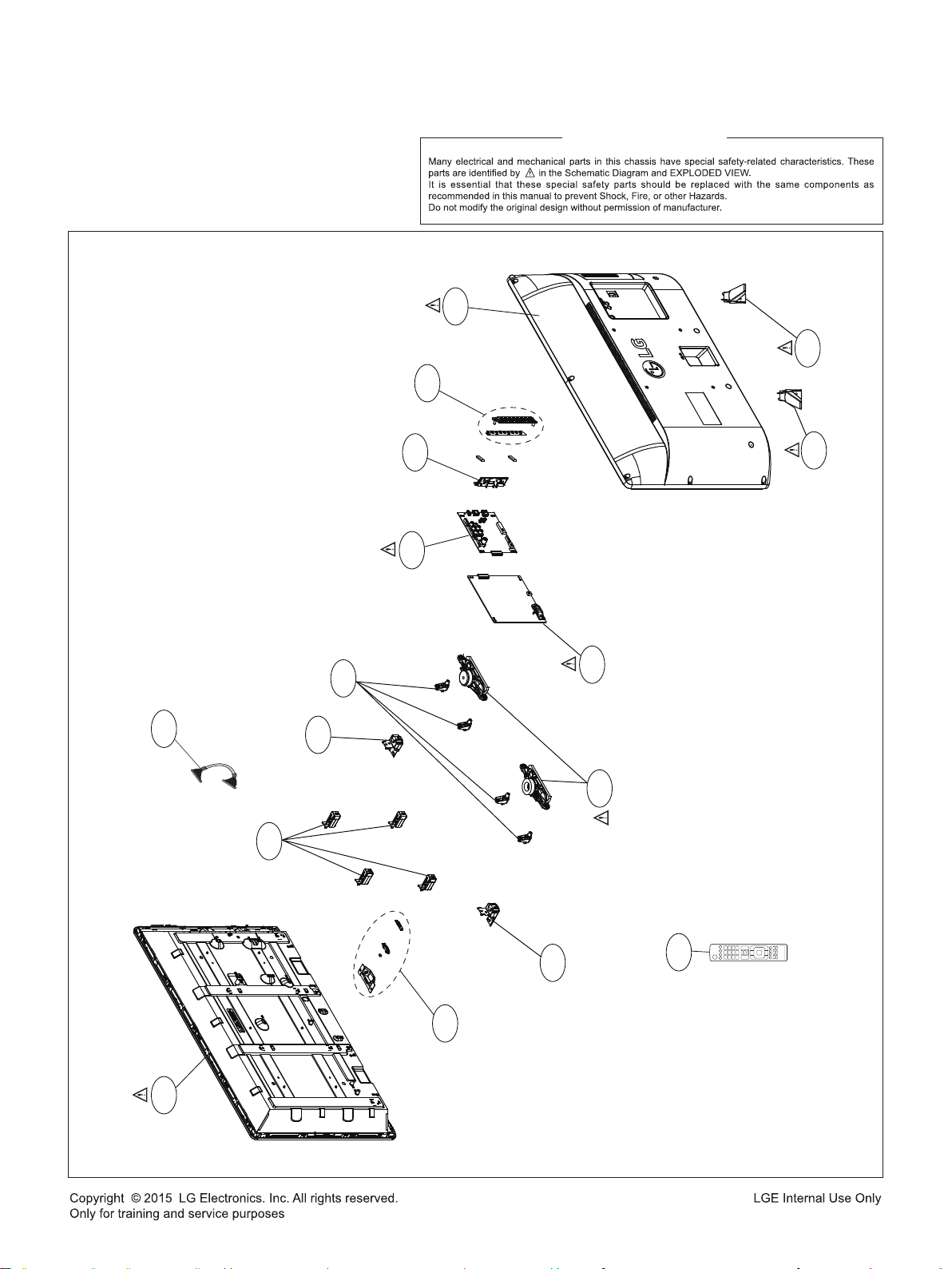
EXPLODED VIEW
IMPORTANT SAFETY NOTICE
400
510
900
840
830
130
521
540
901
530
120
831
500
200 LV1
A2
- 15 -
Page 16

APPENDIX-Schematic-Key board
^^+
1
PCB3
PCB3
0F
0F
0F
of
of
404xxx
404xxx
404xxx
of
22Tuesday, March 10, 2015
22Tuesday, March 10, 2015
22Tuesday, March 10, 2015
1
_
OK
SETTING
INPUT
POWER
KEY PCB
KEY PCB
VTV-K23106 REV:0F
VTV-K23106 REV:0F
CN701
2
45
CN701
AMA-1257-3AW-S
CN701
AMA-1257-3AW-S
KEY1
3
4
KEY1
0.997V 0V2.000V2.993V
R702
R702
1.74K/1%
1.74K/1%
2 4
2 4
S708
123
KEY0
1 3
POWERSETTING
1 3
INPUT
S707
S701
SW PUSH/4P/1.5MM
S701
SW PUSH/4P/1.5MM
S702
SW PUSH/4P/1.5MM
S702
SW PUSH/4P/1.5MM
S706
KEY0
0.997V 0V2.000V2.993V
R706
R706
S705
1.74K/1%
1.74K/1%
2 4
2 4
S704
S703
_
1 3
S705
S705
+
1 3
S706
S706
S702
SW PUSH/4P/1.5MM
SW PUSH/4P/1.5MM
SW PUSH/4P/1.5MM
SW PUSH/4P/1.5MM
S701
KEY1
KEY0
OK
3V
^
^
COMPAL OPTOELECTRONICS CO., LTD
COMPAL OPTOELECTRONICS CO., LTD
COMPAL OPTOELECTRONICS CO., LTD
SCHEMATIC,KEY/B VTV-K32106
SCHEMATIC,KEY/B VTV-K32106
SCHEMATIC,KEY/B VTV-K32106
2
Size Document Number Rev
Date: Sheet
Size Document Number Rev
Date: Sheet
Size Document Number Rev
Date: Sheet
POWER
3
_
0V
4
SETTING
2V
INPUT
+
1V
Title
Title
Title
R703
6.19K/1%
R703
6.19K/1%
R704
39.2K/1%
R704
5
39.2K/1%
D D
Only for training and service purposes
2 4
2 4
- 16 -
^
1 3
S707
SW PUSH/4P/1.5MM
S707
SW PUSH/4P/1.5MM
^
1 3
S708
SW PUSH/4P/1.5MM
S708
SW PUSH/4P/1.5MM
B B
A A
5
LGE Internal Use OnlyCopyright © LG Electronics. Inc. All rights reserved.
R707
6.19K/1%
R707
2 4
2 4
OK
1 3
1 3
S703
SW PUSH/4P/1.5MM
S703
SW PUSH/4P/1.5MM
S704
SW PUSH/4P/1.5MM
S704
SW PUSH/4P/1.5MM
6.19K/1%
R708
39.2K/1%
R708
39.2K/1%
C C
Page 17
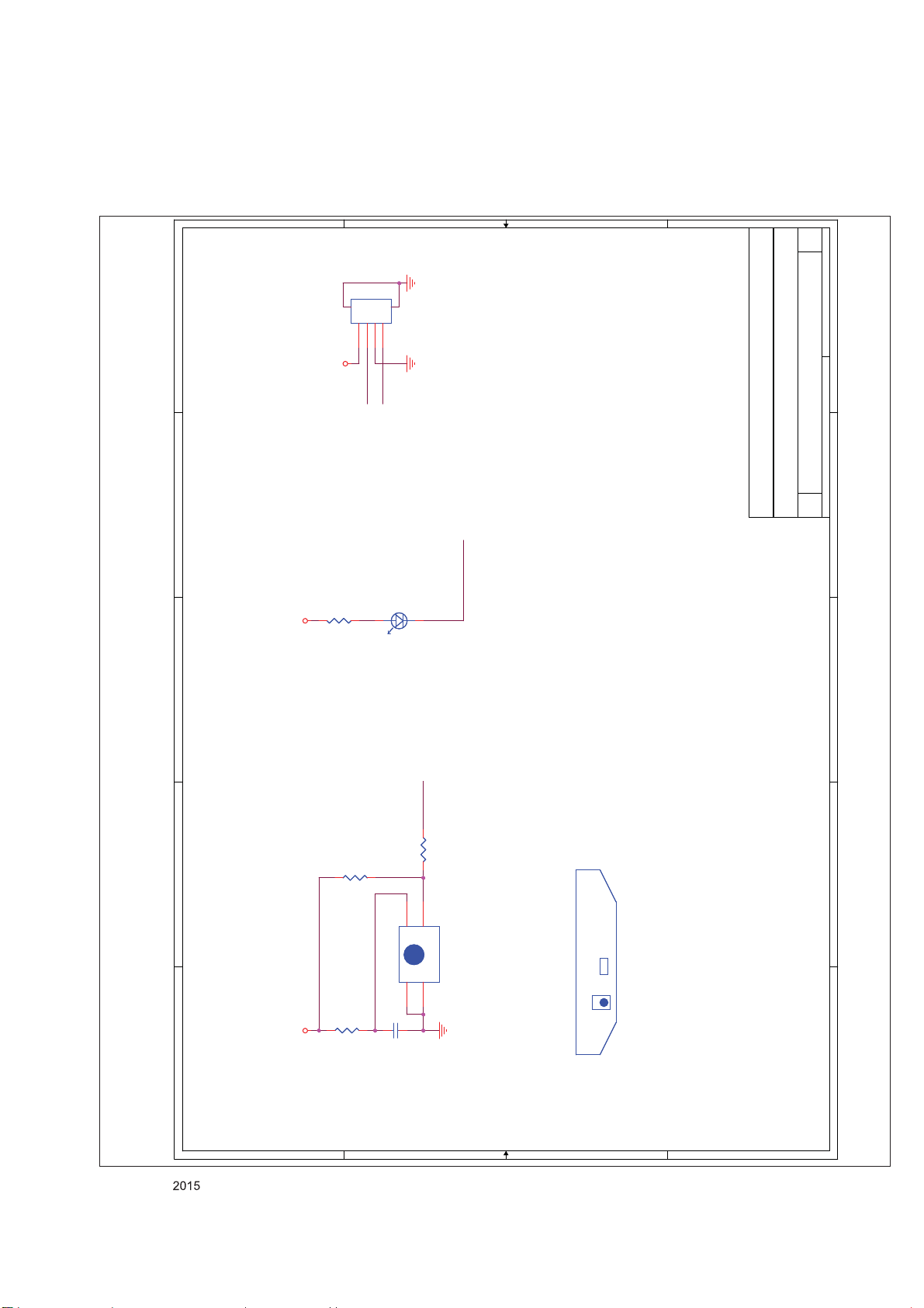
APPENDIX-Schematic-IR/LED board
1
CN1
AMA-1257-4AV-S
CN1
AMA-1257-4AV-S
123
5 6
4
0E
0E
0E
of
of
of
22Tuesday, March 10, 2015
22Tuesday, March 10, 2015
22Tuesday, March 10, 2015
1
+3.3V_Standby
IR_Data
LED_R
XXXXXX
XXXXXX
XXXXXX
)52173$1(/&211(&725
COMPAL OPTOELECTRONICS CO., LTD
COMPAL OPTOELECTRONICS CO., LTD
COMPAL OPTOELECTRONICS CO., LTD
SCHEMATIC,IR/B VTV-IR32106
SCHEMATIC,IR/B VTV-IR32106
SCHEMATIC,IR/B VTV-IR32106
2
LED_R
Title
Title
Title
Size Document Number Rev
Size Document Number Rev
Size Document Number Rev
2
Date: Sheet
Date: Sheet
Date: Sheet
RED LED
LED
+3.3V_Standby
3
12
1K
R81KR8
LED2
LED2
LTST-C171KRKT
LTST-C171KRKT
IR_Data
3
4
REMOTE
5
D D
Only for training and service purposes
R147R1
47
4
R11
10K
R11
10K
IR/LED PCB
4
VCC3OUT
GND
GND
U1
IRM-H638M/TR2
U1
IRM-H638M/TR2
2
1
R5
220R5220
+3.3V_Standby
C4
2.2uF/6.3VC42.2uF/6.3V
C C
- 17 -
IR/LED PCB
PCB2
PCB2
B B
LED
LED
IR
IR
VTV-IR23106 REV:0E
VTV-IR23106 REV:0E
5
A A
LGE Internal Use OnlyCopyright © LG Electronics. Inc. All rights reserved.
Page 18

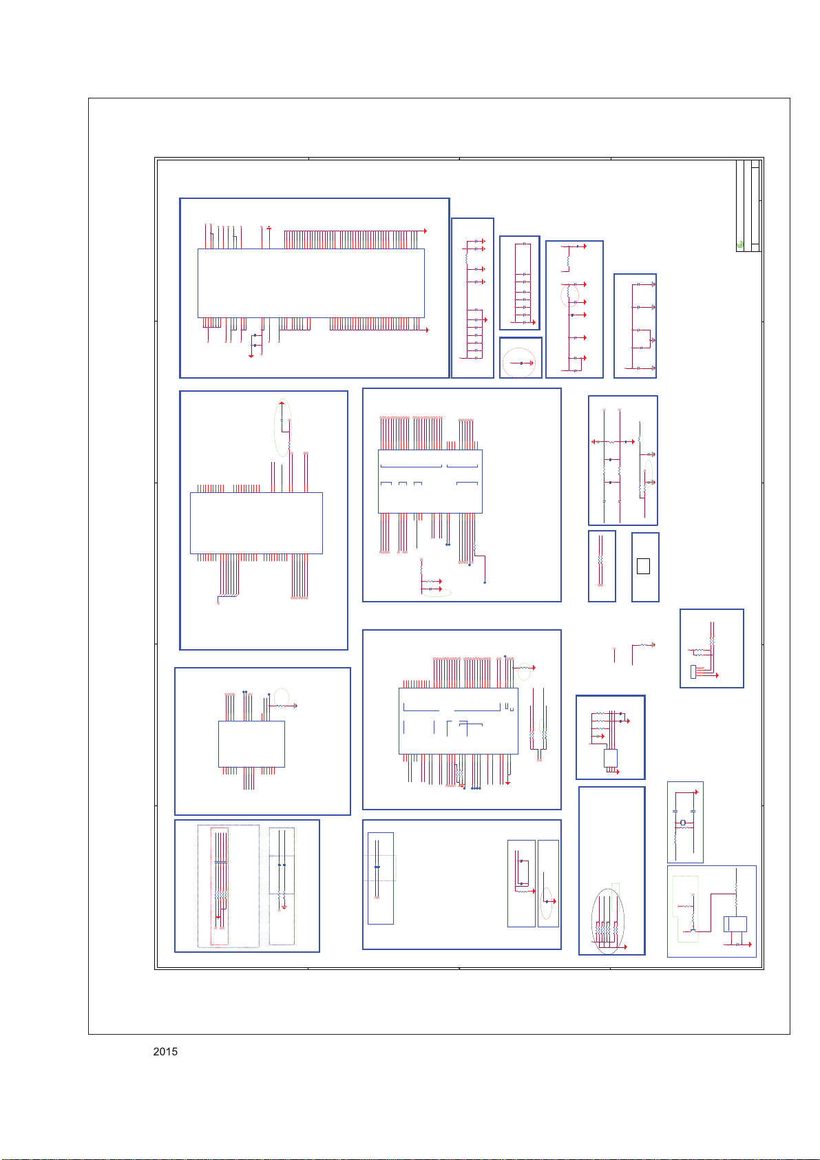
APPENDIX-Schematic-Main board
22uF/10V/0805
22uF/10V/0805
C23
C23
1 2
100uF/6D3/16V/NC
100uF/6D3/16V/NC
C227
+5V_Normal
PN:SE042104K0J
C13 0.1uF/50V/NCC13 0.1uF/50V/NC
1
BS
IN
AN_SY8113/NC
AN_SY8113/NC
5
FB27
FB27
CLS UPB201212T-121Y-N 5A/NC
CLS UPB201212T-121Y-N 5A/NC
+12V_Normal
5.08V
FB14
CLS/0603/60/3A/NC
FB14
CLS/0603/60/3A/NC
L14
L14
ATPI04033R3MTB 4.7uH/2.5A/NC
ATPI04033R3MTB 4.7uH/2.5A/NC
C213 47pF/50V/NCC213 47pF/50V/NC
6
SW
R260
100K/1%/NC
R260
100K/1%/NC
C16
C16
0.1uF/10V/0402/NC
0.1uF/10V/0402/NC
C15
C15
10uF/25V/1206/NC
10uF/25V/1206/NC
100uF/6D3/16V/NC
100uF/6D3/16V/NC
C226
C226
+
+
+1.5V_DDR power from +5V_Normal
R1201
2.7
R1201
2.7
+5V_Normal
C227
C22
C22
100uF/6D3/16V/NC
100uF/6D3/16V/NC
C218
C218
RA
R18 13.6K/1%/0402/NCR18 13.6K/1%/0402/NC
3
FB
GND
EN
4
for DDR3 STR
12/29 Add R1201
+
+
22uF/10V/0805
22uF/10V/0805
1 2
+
+
RB
R13 1.82K/1%/0402/NCR13 1.82K/1%/0402/NC
PN:SA08113000I
FP:TSOT23-6
2
RB=(0.6V/ (Vout-0.6V))xRA
Vout=5.08V
C200
C200
0.1uF/25V/NC
0.1uF/25V/NC
R191 0/0402/NCR191 0/0402/NCC1289
PWR_ON_OFF
PWR_ON_OFF
14,3,4
Reserve for +16V only
+1.5V_DDR
VPP
VPP
4
1uF/16V
C1289
1uF/16V
(2.4/0603) for reduce
ripple voltage when
USB shorting.
C C
1
+3.3V_Standby
FB6
PBY160808T-500Y 3A
FB6
PBY160808T-500Y 3A
C36
0.1uF/10V/0402/NC
C36
C37
C37
RA
C100
10nF/16V/0402
C100
10nF/16V/0402
R378 8.2K/1%R378 8.2K/1%
3
5
LX
VFB
GND
VIN4EN
1
C35
C35
C20
C20
FB5
PBY160808T-500Y 3A
FB5
PBY160808T-500Y 3A
C9
Vout= 1.17V MAX 2A
C8
C7
R122 200K/1%R122 200K/1%
RA
ATPI04033R3MTB 3.3uH/2.5AL1ATPI04033R3MTB 3.3uH/2.5A
R383 12.4K/1%R383 12.4K/1%
C6 68pF/50V/0402C6 68pF/50V/0402
3
5
6
LX
NC
VFB
GND
VIN4EN
G5719CTB1U
G5719CTB1U
1
C3
C2
FB10FB1
0
D D
0.1uF/10V/0402/NC
10uF/6.3V
10uF/6.3V
RB
R379
1.8K/1%
R379
1.8K/1%
Vout=0.6 x (1+(RA/RB))
2
0.1uF/10V/0402
0.1uF/10V/0402
10uF/25V
10uF/25V
9/10 Cost and Package
down C20 grade from
solid E-Cap.
22uF/6.3V/0805C922uF/6.3V/0805
VDDCVDI0
1 2
22uF/6.3V/0805C822uF/6.3V/0805
1 2
22uF/6.3V/0805C722uF/6.3V/0805
1 2
D
D
Q7
Q7
G
G
2N7002
2N7002
R119
R119
R121 200K/1%R121 200K/1%
+3.3V_Standby
R120
R120
R384
12.7K/1%
R384
12.7K/1%
4.7K/0402
4.7K/0402
VID0
RB
4
2
0.1uF/10V/0402C30.1uF/10V/0402
10uF/25VC210uF/25V
U14
U14
+5V_NORMAL
1.24V
H
L 1.17V
S
S
VGS > 2V
4.7K/0402
4.7K/0402
Vout=0.6 x (1+(RA/RB)
3.3Vstb
2
L4
ATPI04033R3MTB 3.3uH/2.5AL4ATPI04033R3MTB 3.3uH/2.5A
+3.3V_Standby power from +5V_Standby
U11
G5728BTO1U
U11
G5728BTO1U
+5V_Standby
R3
33K/1%R333K/1%
3
+5V_Standby
+1.15V_VDDC
4
L1
+1.15V_VDDC power from +5V_Normal
U13
U13
R1
+5V_Normal
33K/1%R133K/1%
5
+5V_Normal
(5V)
+5V_Normal
L9
ATPI04033R3MTB 3.3uH/2.5AL9ATPI04033R3MTB 3.3uH/2.5A
C158
0.1uF/10V/0402
C158
0.1uF/10V/0402
7
6
+5V_Normal power from +12V
SW
BOOT
VIN8EN
VREG
U6
BD9D321EFJU6BD9D321EFJ
1
3
R192 0/0402R192 0/0402
Vout=(RAx0.6)/RB+0.6
R1261
39K/0.5%/0402
R1261
39K/0.5%/0402
1
POK
POK
IC124
IC124
+5V_Normal
+12V_Normal
+12V_Normal
C1281
C1281
RA
1 2
R1259
R1259
679
VO
VO
ADJ
ADJ
UREG
UREG
VEN
VEN
238
0
1 2
R12410R1241
PWR_ON_OFF
14,3,4
C17
0.1uF/25V
C17
0.1uF/25V
C24
C24
C91
C91
C92
C92
C1282
C1282
1 2
1 2
1 2
2.2K/0.5%/0402
2.2K/0.5%/0402
Thermo Pad
Thermo Pad
GND
GND
VIN
VIN
G9661-25ADJF11U
G9661-25ADJF11U
1 2
C1280
C1280
10uF/10V
10uF/10V
RA
R177
3.3K/1%/0402
R177
3.3K/1%/0402
R172
R172
2
FB
TP-GND
9
GND
SS
5
4
C26
C26
3.3nF/50V/0402
3.3nF/50V/0402
C51
C51
1uF/6.3V
1uF/6.3V
C18
0.1uF/16V/0402
C18
0.1uF/16V/0402
C14
C14
10uF/16V/0805
10uF/16V/0805
C19
C19
10uF/16V/0805
10uF/16V/0805
10uF/25V
10uF/25V
10uF/25V
10uF/25V
10uF/25V
10uF/25V
22uF/6.3V/0805
22uF/6.3V/0805
22uF/6.3V/0805/NC
22uF/6.3V/0805/NC
RB
1 2
R1260
47K/0.5%/0402
R1260
47K/0.5%/0402
Vout=(0.8*(RA+RB))/RB
C27
22uF/10V/0805
C27
22uF/10V/0805
C50
22uF/10V/0805
C50
22uF/10V/0805
RB
R176
22K/1%/0402
R176
22K/1%/0402
120K/1%/0402
120K/1%/0402
Vout=0.765 x ( (1+RA)/RB)
R1657
R1657
+3.3V_Normal
+3.3V_Normal from +3.3V_Standby
Ctrl by +5V_Normal
12
12
C1654
C1654
DS
G
Q1653
DMG2301U-7
Q1653
DMG2301U-7
1 2
C1655
33nF/25V/0402
C1655
33nF/25V/0402
12
R1660
R1660
10K/0402
10K/0402
MPZ1608S221AT
MPZ1608S221AT
1 2
FL169
FL169
+3.3V_Standby
B B
1A
1A
1A
of
of
of
315Wednesday, June 10, 2015
315Wednesday, June 10, 2015
315Wednesday, June 10, 2015
1
401C7Z
401C7Z
401C7Z
COMPAL OPTOELECTRONICS CO., LTD
COMPAL OPTOELECTRONICS CO., LTD
COMPAL OPTOELECTRONICS CO., LTD
SCHEMATIC,M/B VTV-L32107
SCHEMATIC,M/B VTV-L32107
SCHEMATIC,M/B VTV-L32107
Title
Size Document Number Rev
Date: Sheet
Title
Size Document Number Rev
Date: Sheet
Title
Size Document Number Rev
Date: Sheet
12/29 Delete DCD which drawing by Stony
2
C195
0.1uF/10V/0402/NC
C195
0.1uF/10V/0402/NC
2
1
+1.2V_MCP
C194
10uF/6.3V
C194
10uF/6.3V
4
VOUT2VOUT
1
GND
VIN
U3
G912T63UU3G912T63U
3
C196
0.1uF/10V/0402
C196
0.1uF/10V/0402
2
1
C193
C193
10uF/25V
10uF/25V
FB32
PBY160808T-500Y 3A
FB32
PBY160808T-500Y 3A
+5V_Normal
+1.2V_MCP from +5V_Normal
for ASIA demodulation
330/1%
330/1%
0.1uF/10V0402
0.1uF/10V0402
1SS355VMTE-17
1SS355VMTE-17
220K/1%/0402
220K/1%/0402
D1652
D1652
1 2
A C
R1661
R1661
C
E
Q1654
2SC4081UB TLQ
Q1654
2SC4081UB TLQ
R1658
R1658
B
10K/0402
10K/0402
12
C1659
0.1uF/10V/0402
C1659
0.1uF/10V/0402
3.3K/1%/0402
3.3K/1%/0402
1 2
1 2
C1660
C1660
4.7uF/25V/0805
4.7uF/25V/0805
C1656
1uF/16V
C1656
1uF/16V
1 2
R1659
R1659
+5V_Normal
A A
3
4
5
Only for training and service purposes
- 18 -
LGE Internal Use OnlyCopyright © LG Electronics. Inc. All rights reserved.
Page 19
靠近
晶體頻偏需要小於
AVDD_AU
+3.3V_Standby
+3.3V_Standby
1
2
3
4
5
AVDD_DVI
AVDD_NODIE
L7
R6
J7
AVDD_AU33
AVDD_NODIE
AVDD_DVI_USB_MPLLK7AVDD_DVI_USB_MPLL
VDDC
VDDC
VDDC
VDDC
VDDC
VDDC
VDDC
U201F
U201F
L11
P12
P13
N12
N13
N14
N15
M11
+1.15V_VDDC
POWER&GND
W14
W13
W11
Y15
Y13
Y12
Y14
W12
AA12
AA13
TS0_D0
TS0_D1
TS0_D2
TS0_D3
TS0_D4
TS0_D5
TS0_D6
TS0_D7
TS0_CLK
U201B
U201B
PCM_D0
PCM_D1
PCM_D2
PCM_D3
PCM_D4
PCM_D5
PCM_D6
PCM_D7
T16
T14
V15
Y20
Y21
Y18
U20
W18
AA18
PCM_A0
PCM_A[7:0]
NAND & CI & TS & Front End
12
U201E
U201E
GIN1N
RIN1
C209 47nF/16V/0402C209 47nF/16V/0402
C207 47nF/16V/0402C207 47nF/16V/0402
Close to MST IC
with wide trace
8
R205 68/0402R205 68/0402
R212 33/0402R212 33/0402
YPBPR
YPbPr-PR
RGB Interface
video
GIN1
C210 47nF/16V/0402C210 47nF/16V/0402
R206 33/0402R206 33/0402
AVDD_DMPLL
+3.3V_Normal
+3.3V_Normal
+3.3V_Normal
VDDP
AVDD_MOD
R5
R16
R17
R15
R18
VDDP
AVDD_MOD
AVDD_MOD
AVDD3P3_DMPLL
VDDC
AVDDL_MOD
DVDD_RX_1
P14
M12
M14
M13
+1.15V_VDDC
+1.15V_VDDC
+1.15V_VDDC_RX
T13
U13
T12
U10
Y11
TS1_D0
TS1_D1
TS1_D2
TS0_VLD
TS0_SYNC
PCM_A0
PCM_A1
PCM_A2
PCM_A3
PCM_A4
PCM_A5
PCM_A6
PCM_A7
Y17
Y16
Y19
W17
W16
W15
AA16
AA15
PCM_A6
PCM_A1
PCM_A7
PCM_A2
PCM_A3
PCM_A4
PCM_A5
13
MDI_RP13MDI_RN13MDI_TN13MDI_TP
MDI_RP
MDI_TP
MDI_RN
MDI_TN
C1
B2
C2
B1
TP
TN
RP
RN
GIN0PL3GIN0ML2HSYNC0M5VSYNC0M4GIN1PN3SOGIN1
RIN0PM3BIN0PK2RIN1PN2GIN1MN1BIN1P
SOG1
BIN1
C204 1nF/25V/0402C204 1nF/25V/0402
C211 47nF/16V/0402C211 47nF/16V/0402
1/22 Add R209 , change
C204 from 47nF to 1nF as
M-Star recommend.
4,8
8
R208 33/0402R208 33/0402
R209 0/0402R209 0/0402
YPbPr-Y
YPbPr-PB
D D
AVDD_PLL
AVDD_PLL
DVDD_RX_1A7DVDD_RX_2
T11
TS1_D3
PCM_A8
AA19
1
USB0_DM
C4
RIN1
DVDD_RX_2B7DVDD_DDR
DVDD_DDR
C7
U11
T10
TS1_D4
TS1_D5
PCM_A9
PCM_A10
W21
AA20
TP8TP 8
TP7TP 7
1
USB1_DM
USB0_DP
B4
Y10
DP_P0
DM_P0
RGB
RGB
GIN1N
GIN1
C281
C281
C283
C283
V12
V13
U12
TS1_D6
TS1_D7
TS1_CLK
PCM_A11
PCM_A12
PCM_A13
V20
V17
W20
9
USB1_DM9USB1_DP
USB1_DP
W10
DP_P1
DM_P1
USB
USB
M1
M2
SOG1
BIN1
AVDD5V_MHL_C
V6
H7
GND_EFUSE
AVDD5V_MHL
DVDD_NODIEF8AVDD_DDR0_DC5AVDD_DDR0_D
MCP_VDDC
MCP_VDDC
P11
N11
0.1uF/10V/0402
0.1uF/10V/0402
1uF/6.3V
1uF/6.3V
DVDD_NODIE
+1.2V_MCP
04/17 EMI solution
add R213 0/0402 and
C231 NC
VIFP
VIFM
V10
W1
W2
VIFP
TS1_VLD
TS1_SYNC
PCM_IOWR_N
PCM_RESET
PCM_IRQA_N
PCM_OE_N
PCM_A14
T15
V16
U17
U16
W19
TP211TP211
1
CVBS0
VCOM0
T2
R1
T1
VCOM0
CVBS0PT3CVBS1P
CVBS_OUT
CVBS PHY
CVBS PHY
RIN2PR2GIN2MR3GIN2PP2BIN2PP3HSYNC2K4VSYNC2
M6
Close to MST IC
with wide trace
AV Interface
K10
L10
J10
J11
J12
J13
J14
K8
GND
GND
GND
GND
GND
GNDK9GNDL8GND
AVDD_DRAMB5AVDD_DRAM
B6
11
T_SDA
Y1
T_I2C_SDA
MSD8832RKM2 BGA-402 ball
MSD8832RKM2 BGA-402 ball
U7
NAND_RBZ
video level check
L9
GND
GND
GNDM7GNDM8GNDM9GND
GND
GND
GND
GND
GND
GNDA6GNDC9GND
A13
A15
A18
B12
B14
B16
M10
GND
GND
B17
B19
H17
H18
H11
H12
H13
H14
H15
H16
GND
GND
GNDJ8GNDJ9GND
GND
GND
GND
GND
GND
GND
AVDD_DDR0_D
AVDD_DDR0_CMD
AVDD_DDR1_DC6AVDD_DDR1_D
AVDD_DDR1_D
AVDD_DDR1_CMD
AVDD_DDR1_CLK
L12
L14
L13
K12
K11
K14
K13
+1.5V_DDR
6
EEPROM_WP
C231
C231
10pF/50V/0402/NC
10pF/50V/0402/NC
11
T_SCL11T_SDA
RF_SW_CTL
R213 0/0402R213 0/0402
IFAGC
T_SCL
RF_SW_CTL
Y2
AA4
Y4
Y3
VIFM
IFAGC
TGPIO0
TGPIO1
T_I2C_CLK
PCM_WAIT_N
PCM_IORD_N
PCM_CE_N
PCM_WE_N
PCM_CD_N
PCM_REG_N
NAND_ALET8NAND_WPZT9NAND_CEZV7NAND_CLEU9NAND_REZV9NAND_WEZU8NAND_RBZ
V21
V19
V18
U15
U14
NAND_ALE
NAND_CLE
NAND_WPZ
NAND_CEZ
NAND_REZ
NAND_WEZ
NAND_ALE12NAND_CLE
NAND_WPZ12NAND_CEZ12NAND_REZ12NAND_RBZ12NAND_WEZ
12
12
R7
75/1%/0402R775/1%/0402
03/19 Add R7
(75-ohm) for A71 do
MSD8832RKM2 BGA-402 ball
MSD8832RKM2 BGA-402 ball
CVBS0
VCOM0
C217 47nF/16V/0402C217 47nF/16V/0402
C216 47nF/16V/0402C216 47nF/16V/0402
R216 33/0402R216 33/0402
R217 68/0402R217 68/0402
YPbPr-Y
4,8
N10
P10
P15
P16
P17
P18
R11
R12
R13
R14
GNDN4GNDN5GNDN6GNDN7GNDN8GNDN9GND
GNDP4GNDP5GNDP6GNDP7GND
GND
GND
GND
GNDD9GND
GND
GND
GND
F11
F13
F15
F17
B20
E20
C10
C21
GPIO & LVDS
LINE_IN_1L
C222 2.2uF/6.3V/0402C222 2.2uF/6.3V/0402
HD-LIN
Audio Line IN
U6
GND
GND
GND
GND
GNDR7GND
GND
GND
GND
GNDR4GNDT6GNDT7GND
GND
GND
GND
GNDG9GND
GND
GND
GND
GND
GND
GND
GND
GND
GNDH8GNDH9GND
GND
G8
F19
F21
G10
G11
G12
G13
G14
G15
G16
G17
G18
LVA0N6LVA0P6LVA1N6LVA1P6LVA2N6LVA2P6LVACLKP6LVACLKN6LVA3N6LVA3P6LVA4N6LVA4P6LVB0N6LVB0P6LVB1P6LVB1N6LVB2N6LVBCLKN6LVBCLKP6LVB2P6LVB3P6LVB3N6LVB4P6LVB4N
LVA0P
LVA2P
LVA4P
LVA3P
LVA1P
LVACLKP
LVA2N
LVA3N
LVA4N
LVACLKN
LVA1N
LVA0N
LVB0P
LVB0N
N21
P19
R19
T21
U19
J19
N19
N20
P20
T19
T20
H20
R20
R21
LVA0P
LVA1P
LVA2P
LVA3P
LVA4P
LVB0P
LVA0N
LVA1N
LVA2N
LVA3N
LVA4N
LVB0N
LVACKP
LVACKN
PWM SAR SPI
PWM SAR SPI
U201D
U201D
KEY0F4LED_RD4ARC_DETG73D_EN/PCM_PWR_EN
AMP_MUTE
BRI_ADJ
PM_SPI_CKD6PM_SPI_DIE7PM_SPI_DOD7UART0_RXL5UART0_TXL4M_I2C_SLC
PWM_PM
SAR3G5PM_SPI_CZ1N
K5
T18
T17
U18
ARC_DET
ACDET_M
BRI_ADJ
AMP_MUTE
SPI_SDI
ARC_DET7
BRI_ADJ
PWM_LED1
PWM_LED2
AMP_MUTE
SAR0_KEY_114SAR3_KEY_2
14
14
14
10
14
H2
J2
K3
J3
J1
K1
U201C
U201C
A_RX0P
A_RX1P
A_RX2P
A_RX0N
A_RX1N
A_RX2N
LINE_IN_3LV4LINE_IN_3R
U4
LINE_IN_1L
LINE_IN_1R
LINE_IN_1R
mstar IC
C223 2.2uF/6.3V/0402C223 2.2uF/6.3V/0402
HD-RIN
HD-LIN
HD-RIN
8
8
H10
LVB2P
LVB1P
LVB2N
LVB1N
J21
K21
J20
K19
LVB1P
LVB1N
LVB2N
LVDS
LVDS
F7
14
C_ACDET
R148
100/0402
R148
100/0402
R149 100/0402/NCR149 100/0402/NC
C234 33pF/50V/0402C234 33pF/50V/0402
ACDET_M
H3
H5
G2
A_RXCP
A_RXCN
DDCDA_CKH6DDCDA_DA
LINE_OUT_0LV2LINE_OUT_0RV1LINE_IN_1LU5LINE_IN_1RV5LINE_IN_2LT5LINE_IN_2RT4VAGV3VRM
LINE_OUT_L
LINE_OUT_R
MSD8832RKM2 BGA-402 ball
MSD8832RKM2 BGA-402 ball
LVBCLKP
LVBCLKN
K20
L19
LVB2P
LVBCKN
UART_RX
G4
HOTPLUGA
W4
EARPHONE_L
EARPHONE_R
HDMI & Audio
C C
C242
C242
+1.15V_VDDC_RX
C246
C246
FB205
FB205
BLM15AG601SN1D
BLM15AG601SN1D
C245
C245
AVDDL_MOD
C244
C244
C243
C243
C236
C236
C241
C241
CORE POWER
C240
C240
C239
C239
C238
C238
+1.15V_VDDC
C237
C237
10
8
7
6
AMP_RESET
HDMI-2_SENSE7COMPONENT_INS
CVBS_INS8HDMI-3_SENSE
LVDS_SEL 6
LVB3P
LVB4P
LVB3N
LVB4N
M19
M21
G20
H19
G19
L20
M20
G21
J16
J17
J15
K17
J18
K18
K16
L18
LDE
LCK
LVB3P
LVB4P
LVB3N
LVB4N
TCON0
TCON1
TCON2
TCON3
TCON4
TCON5
TCON6
LVBCKP
UART_TX
TCON7
LVSYNC
LHSYNC
TCON
TCON
GPIO_PM
GPIO_PM
M_I2C_SDA
UART_RX2
UART_TX2
VID0W3PANNEL_ON/OFFE8PWR_ON/OFFD1VBL_CTRLD8PMCONFIG0U33D_LR_IND5PMCONFIG1
G6
L15
L16
L17
K15
UART2_TX
UART2_RX
M_I2C_SCL
M_I2C_SDA
PM_CONFIG1
/PM_CONFIG0
1
1
TP205TP205
TP203TP203
R279 0/0402/NCR279 0/0402/NC
M_WLAN_POWER
EARPHONE_DEC_M
1
VID03
TP1TP 1
VBL_CTRL14
PWR_ON_OFF14,3
PANEL_ON_OFF6
EARPHONE_DEC_M 8
01/12 Modify C234 to 0402 to common part.
HDMI2_RX0N 7
HDMI2_RX0P 7
HDMI2_RX1N 7
HDMI2_RX1P 7
HDMI2_RX2N 7
HDMI2_RX2P 7
HDMI2_CLKP 7
HDMI2_CLKN 7
HDMI3_RX0N 7
HDMI3_RX0P 7
HDMI3_RX1N 7
HDMI3_RX1P 7
HDMI3_RX2N 7
HDMI3_RX2P 7
HDMI2_SDA 7
HDMI2_SCL 7
HDMI2_HPDIN 7
HDMI2_CLKN
HDMI2_RX1N
HDMI2_CLKP
HDMI2_RX1P
HDMI2_RX2N
HDMI2_RX0P
HDMI2_RX2P
HDMI2_RX0N
HDMI3_RX0P
HDMI3_RX1N
HDMI3_RX1P
HDMI3_RX2N
HDMI3_RX0N
HDMI3_RX2P
HDMI3_CLKN
HDMI2_SCL
HDMI2_SDA
HDMI2_HPDIN
Y6
AA7
D2
AA6
Y8
Y9
W9
F3
F1
G1
Y7
W7
W8
AA9
E2
F2
G3
C_RX0P
C_RX1P
C_RX2P
D_RX0P
D_RX1P
C_RX1N
C_RX2N
HDMI
HDMI
Analog audioI2S
Analog audioI2S
I2S_OUT_BCKA3I2S_OUT_SD
U2
AUVAG
AUVRM
I2S-OUT_BCK
I2S-OUT_MCK
I2S-OUT_MCK10I2S-OUT_WS10I2S-OUT_BCK10I2S-OUT_SD
D_RX2P
D_RX0N
D_RX1N
D_RX2N
C_RXCP
C_RXCN
HOTPLUGC
DDCDC_CKW6DDCDC_DA
I2S_OUT_MCKB3I2S_OUT_WS
I2S_IN_WS/T2_RESETE4I2S_IN_BCK/T2_I2CS_SCLF5I2S_IN_SD/T2_I2CS_SDA
SPI1_DIP9SPI1_CKR8SPI2_DIR9SPI2_CK
A2
E5
C3
R10
10
I2S-OUT_WS
SPI2_DI
SPI1_CK
SPI1_DI
SPI2_CK
I2S-OUT_SD
R145 4.7K/0402R145 4.7K/0402
R147 4.7K/0402R147 4.7K/0402
R146 4.7K/0402R146 4.7K/0402
1
1
1
1
TP208TP208
TP207TP207
TP212TP212
TP209TP2091TP210TP210
+3.3V_Standby
C_RX0N
EARPHONEOUTRY5EARPHONEOUTL
HDMI3_CLKN 7
HDMI3_CLKP 7
HDMI3_CLKP
E3
D_RXCN
demod
demod
1A
1A
1A
of
of
of
415Wednesday, June 10, 2015
415Wednesday, June 10, 2015
415Wednesday, June 10, 2015
401C7Z
401C7Z
401C7Z
0.1uF/10V/0402
0.1uF/10V/0402
0.1uF/10V/0402
0.1uF/10V/0402
0.1uF/10V/0402/NC
0.1uF/10V/0402/NC
0.1uF/10V/0402/NC
0.1uF/10V/0402/NC
0.1uF/10V/0402/NC
0.1uF/10V/0402/NC
10uF(M)/6.3V/0603/NC
10uF(M)/6.3V/0603/NC
0.1uF/10V/0402
0.1uF/10V/0402
0.1uF/10V/0402
0.1uF/10V/0402
0.1uF/10V/0402
0.1uF/10V/0402
0.1uF/10V/0402
0.1uF/10V/0402
2.2uF/6.3V/0402
2.2uF/6.3V/0402
MSD8832RKM2 BGA-402 ball
MSD8832RKM2 BGA-402 ball
1
M_WWOL_WAKEUP
TP2TP 2
HDMI3_SDA 7
HDMI3_SCL 7
HDMI3_HPDIN 7
HDMI3_SCL
HDMI3_SDA
HDMI3_HPDIN
HDMI_ARC
K6
L6
J5
D_RXCP
HOTPLUGD
DDCDD_CKJ4DDCDD_DA
IRINF6RESETD3XTALIN
IRIN
System_RST
DDR3 POWER
nodie
TP213TP213
SPDIF_OUT 8
HDMI_ARC 7
HDMI_CEC 7
1
SPDIF_OUT
HDMI_CEC
E6
A4
J6
CEC
SPDIF_IN
PAD_ARC0
SPDIF_OUT
SPDIF
SPDIF
XTALOUT
TESTPIN
F9
AA2
AA3
XTALI
XTALO
+1.5V_DDR
DVDD_NODIE
MHL_CABLE-DET
AA10
P8
AVDD_DRAM
MHL_VBUS-EN 7
MHL_CABLE-DET 7
MHL_VBUS-EN
W5
MHL_VBUS_EN
MHL_CABLE_DET
MHL
MHL
MCP_TEST
AUVRM
C255
C255
C254
C254
C259
C259
C253
C253
C252
C252
C251
C251
C250
C250
C249
C249
C267
1uF/6.3V
C267
1uF/6.3V
R12
R12
10K/0402
10K/0402
MSD8832RKM2 BGA-402 ball
MSD8832RKM2 BGA-402 ball
C233
4.7uF/6.3V/0402
C233
4.7uF/6.3V/0402
AUVAG
C232
0.1uF/10V/0402
C232
0.1uF/10V/0402
FB201
FB201
BLM15AG102SN1D
BLM15AG102SN1D
0.1uF/10V/0402/NC
0.1uF/10V/0402/NC
0.1uF/10V/0402/NC
0.1uF/10V/0402/NC
0.1uF/10V/0402
0.1uF/10V/0402
0.1uF/10V/0402
0.1uF/10V/0402
0.1uF/10V/0402
0.1uF/10V/0402
0.1uF/10V/0402
0.1uF/10V/0402
2.2uF/6.3V/0402
2.2uF/6.3V/0402
10uF/25V
10uF/25V
Close to MST IC
9/9 add R12 for drag low
MHL_VBUS-EN when Scaler
during reset.
EARPHONE_L
EARPHONE_R
LINE_OUT_L
LINE_OUT_R
R129 0/0402/NCR129 0/0402/NC
R127 1K/1%/0402R127 1K/1%/0402
R126 1K/1%/0402R126 1K/1%/0402
R128 0/0402/NCR128 0/0402/NC
EARPHONE_DRV_L15
EARPHONE_DRV_R15
Close to MSTAR IC
with width trace
SPDIF_OUT
C235
C235
B B
C288
C288
AVDD_AU
FB204
FB204
0.1uF/10V/0402
0.1uF/10V/0402
BLM15AG601SN1D
BLM15AG601SN1D
+3.3V_Standby
C280
C280
0.1uF/10V/0402
0.1uF/10V/0402
AVDD_DMPLL
FB202
FB202
0.1uF/10V/0402/NC
0.1uF/10V/0402/NC
C279
C279
BLM15AG601SN1D
BLM15AG601SN1D
0.1uF/10V/0402/NC
0.1uF/10V/0402/NC
C278
C278
AVDD_NODIEAVDD_DVI
C277
C277
C275
0.1uF/10V/0402
C275
0.1uF/10V/0402
Standby Power 3.3V
+3.3V_Standby
10uF/25V
10uF/25V
C274
C274
+3.3V_Normal
EEPROM ConnectorMode Selection
01/29 R126, R127 from 0 to 1K as M-Star request
for 4Mhz white noise from SOC
Close to MSTAR IC
33pF/50V/0402/NC
33pF/50V/0402/NC
+3.3V_Standby
VDDPAVDD_MOD AVDD_PLL
0.1uF/10V/0402
0.1uF/10V/0402
Normal Power 3.3V
+3.3V_Normal
11
DIFP11DIFM
FB30
PBY160808T-121Y-N 2.5/NC
FB30
PBY160808T-121Y-N 2.5/NC
C228
100pF/25V/0402/NC
C228
100pF/25V/0402/NC
C224
100pF/25V/0402/NC
C224
100pF/25V/0402/NC
C229
C229
100pF/25V/0402/NC
100pF/25V/0402/NC
R137 0/0402R137 0/0402
R136 0/0402R136 0/0402
C230
C230
100pF/25V/0402/NC
100pF/25V/0402/NC
C247 0.1uF/10V/0402C247 0.1uF/10V/0402
C248 0.1uF/10V/0402C248 0.1uF/10V/0402
VIFM
VIFP
RF
M_I2C_SCL
M_I2C_SDAM-SDA
R275 100/0402R275 100/0402
R274 100/0402R274 100/0402R229 4.7K/0402/NCR229 4.7K/0402/NC
M-SCLM_WLAN_POWER
M-SCL
M-SDA
Other
10,14,6
10,14,6
14
IRIN
IRIN
MHL_CABLE-DET
IR&KEYB
R232
4.7K/0402
R232
4.7K/0402
C264
33pF/50V/0402
C264
33pF/50V/0402
4.7K/0402
4.7K/0402
R231
R231
4.7K/0402
4.7K/0402
R244
R244
C263
C263
33pF/50V/0402
33pF/50V/0402
M-SCL
M-SDA
C261
C261
EEPROM_WP
5
6
7
8
WP
0.1uF/10V/0402
0.1uF/10V/0402
SCL
SDA
VCC
A01A12A23GND
U203
FM24C32A-SO-T-G
U203
FM24C32A-SO-T-G
4
PWM_PM Boot_Strap should
link to Scaler K5 (PWM_R)
which assign for LED R.
26Aug2014
// CHIP Config {PM_CONFIG0, SPI_DI, PM_CONFIG1, PWM_PM}
SB51_EXT spi 4'b1000 Boot from 51 EXT SPI flash
/PWM_PM
PM_CONFIG1
PWM_LED1
SPI_SDI
R236 4.7K/0402R236 4.7K/0402
R227 4.7K/0402R227 4.7K/0402
R235 4.7K/0402/NCR235 4.7K/0402/NC
R237 4.7K/0402R237 4.7K/0402
R241 4.7K/0402/NCR241 4.7K/0402/NC
R238 4.7K/0402/NCR238 4.7K/0402/NC
R240 4.7K/0402R240 4.7K/0402
1uF(K)/6.3V/NC
1uF(K)/6.3V/NC
C260
C260
0.1uF/10V/0402
0.1uF/10V/0402
C268
C268
0.1uF/10V/0402
0.1uF/10V/0402
C258
C258
0.1uF/10V/0402
0.1uF/10V/0402
C256
C256
10uF/25V
10uF/25V
C257
C257
+3.3V_TU
FB33
PBY160808T-121Y-N 2.5
FB33
PBY160808T-121Y-N 2.5
C272
0.1uF/10V/0402
C272
0.1uF/10V/0402
IF-AGC-T 11
C262
0.022uF/25V/0402
C262
0.022uF/25V/0402
R228 0/0402R228 0/0402
R226 10K/0402R226 10K/0402
04/08 Modify C262 from 0.1uF to 0.022uF as M-Star ask for.
IFAGC
HeatSink35x35
heat sink
UART_TX
UART_RX
100/0402
100/0402
ISP AND VGA EDID
MUST pull high to 5VSTB
R267
4.7K/0402
R267
4.7K/0402
R270 100/0402R270 100/0402
R271
R271
R245
R245
4.7K/0402/NC
4.7K/0402/NC
HEMCU_EXT spi 4'b1001 Boot from MIPS EXT SPI flash
HEMCU_ROM NAND 4'b1011 Boot from ROM outer storage is nand
+5V_Standby
R268
R268
4.7K/0402
4.7K/0402
1
2
3
4
CN206
CN206
HDR_1X4_H2031_P2
HDR_1X4_H2031_P2
DEBUG
30PPM
11/26 Modify
Y1
24MHz/20pF/S/2P_HARMONYY124MHz/20pF/S/2P_HARMONY
C79 27pF/50V/0402C79 27pF/50V/0402
C77 27pF/50V/0402C77 27pF/50V/0402
NOTE:
R124
R124
1M/1%/0402
1M/1%/0402
R130
R130
XTALI
Crystal
470/1%/0402
470/1%/0402
XTALO
9
USB_Fault
R167
10K/0402/NC
R167
10K/0402/NC
+3.3V_Standby
R202
1K/1%/0402/NC
R202
1K/1%/0402/NC
B
12/08 Add R171 1K/0402
C E
Q15
Q15
+3.3V_Standby
LRC3906/SOT23/NC
LRC3906/SOT23/NC
RESET CIRCUIT
A A
Q15 for USB_Fault
COMPAL OPTOELECTRONICS CO., LTD
COMPAL OPTOELECTRONICS CO., LTD
COMPAL OPTOELECTRONICS CO., LTD
1
SCHEMATIC,M/B VTV-L32107
SCHEMATIC,M/B VTV-L32107
SCHEMATIC,M/B VTV-L32107
Title
Size Document Number Rev
Date: Sheet
Title
Size Document Number Rev
Date: Sheet
Title
Size Document Number Rev
Date: Sheet
2
3
4
System_RST
5
R144
100/0402
R144
100/0402
R171
1K/1%/0402
R171
1K/1%/0402
2
RESET
POR
POR
VCC3GND
U7
G690H293
U7
G690H293
(High reset)
1
C269
C269
+3.3V_Standby
0.1uF/10V/0402
0.1uF/10V/0402
Only for training and service purposes
- 19 -
LGE Internal Use OnlyCopyright © LG Electronics. Inc. All rights reserved.
Page 20

1A
1A
1A
of
of
of
515Wednesday, June 10, 2015
515Wednesday, June 10, 2015
515Wednesday, June 10, 2015
1
2
R62
56/1%/0402/NC
R62
56/1%/0402/NC
B-DDR3-DQU1
B-DDR3-DQL6B_DDR3_DQL6
B-DDR3-DQL4B_DDR3_DQL4
B-DDR3-DQU5B_DDR3_DQU5
B-DDR3-DQU7
7531
7531
7531
7531
7531
7531
8642
8642
8642
8642
8642
RN4 22/0804/MS/NC
RN4 22/0804/MS/NC
22/0804/MS/NC
22/0804/MS/NC
7531
7531
8642
8642
RN3
RN3
8642
R53 22/1%/0402/NCR53 22/1%/0402/NC
RN6 22/0804/MS/NC
RN6 22/0804/MS/NC
B_DDR3_DQU1
B_DDR3_DQU7
B-DDR3-A4
7531
7531
7531
7531
8642
8642
8642
8642
RN7 22/0804/MS/NC
RN7 22/0804/MS/NC
RN5 22/0804/MS/NC
RN5 22/0804/MS/NC
B_DDR3_A4
B_DDR3_A6 B-DDR3-A6
B_DDR3_A10 B-DDR3-A10
B_DDR3_CKE B-DDR3-CKE
RN2 22/0804/MS/NC
RN2 22/0804/MS/NC
B_DDR3_DQL0 B-DDR3-DQL0
B_DDR3_DQL2 B-DDR3-DQL2
3
B-DDR3-BA1
7531
7531
8642
8642
RN1 22/0804/MS/NC
RN1 22/0804/MS/NC
B_DDR3_BA1
B_DDR3_A12 B-DDR3-A12
B-DDR3-DQSLB_DDR3_DQSL
B-DDR3-DQSLBB_DDR3_DQSLB
B-DDR3-DQU3B_DDR3_DQU3
7531
7531
7531
7531
8642
8642
8642
8642
RN8 22/0804/MS/NC
RN8 22/0804/MS/NC
RN10 22/0804/MS/NC
RN10 22/0804/MS/NC
B_DDR3_DMU B-DDR3-DMU
B-DDR3-ODTB_DDR3_ODT
B-DDR3-RASZB_DDR3_RASZ
7531
7531
7531
7531
8642
8642
8642
8642
RN11 22/0804/MS/NC
RN11 22/0804/MS/NC
RN9 22/0804/MS/NC
RN9 22/0804/MS/NC
B_DDR3_A8 B-DDR3-A8
B_DDR3_A11 B-DDR3-A11
B-DDR3-A1B_DDR3_A1
B-DDR3-DQSUB
7531
7531
8642
8642
RN12 22/0804/MS/NC
RN12 22/0804/MS/NC
B_DDR3_DQSUB
B_DDR3_A14 B-DDR3-A14
B-DDR3-DQU4B_DDR3_DQU4
B-DDR3-DQSU
7531
7531
8642
8642
RN14 22/0804/MS/NC
RN14 22/0804/MS/NC
B_DDR3_DQU0 B-DDR3-DQU0
B_DDR3_DQSU
B-DDR3-A13B_DDR3_A13
B-DDR3-A9B_DDR3_A9
7531
7531
7531
7531
8642
8642
8642
8642
RN15 22/0804/MS/NC
RN15 22/0804/MS/NC
RN13 22/0804/MS/NC
RN13 22/0804/MS/NC
B-DDR3-WEZ
B_DDR3_WEZ
7531
7531
8642
8642
RN16 22/0804/MS/NC
RN16 22/0804/MS/NC
B-DDR3-CS0B_DDR3_CS0
B-DDR3-DQL7
B-DDR3-DQL1B_DDR3_DQL1
B-DDR3-DQL3B_DDR3_DQL3
B-DDR3-MCLKZ
B-DDR3-CASZB_DDR3_CASZ
7531
7531
8642
8642
RN21 22/0804/MS/NC
RN21 22/0804/MS/NC
B-DDR3-MCLK
7531
7531
8642
8642
R55 22/1%/0402/NCR55 22/1%/0402/NC
RN22 22/0804/MS/NC
RN22 22/0804/MS/NC
R56 22/1%/0402/NCR56 22/1%/0402/NC
B_DDR3_RESET B-DDR3-RESET
B_DDR3_DML B-DDR3-DML
B_DDR3_MCLK
B_DDR3_MCLKZ
B-DDR3-BA2B_DDR3_BA2
B-DDR3-BA0B_DDR3_BA0
7531
7531
8642
8642
RN23 22/0804/MS/NC
RN23 22/0804/MS/NC
B_DDR3_A3 B-DDR3-A3
B-DDR3-DMU
B-DDR3-DQU0
B-DDR3-DQSU
B-DDR3-DQSUB
C7
D3
B7
U8
K4B2G1646Q-BCMA/NCU8K4B2G1646Q-BCMA/NC
DMU
VDDQ
DQU0D7DQU1C3DQU2C8DQU3C2DQU4A7DQU5A2DQU6B8DQU7
DQSU
A8
/DQSU
VDDQ
A1
VDDQ
C1
VDDQ
C9
VDDQ
D2
VDDQ
E9
VDDQ
F1
VDDQ
H2
VDDQ
H9
VDD
B2
VDD
+1.5V_DDR
D9
VDD
G7
VDD
K2
VDD
K8
VDD
N1
VDD
N9
VDD
R1
VDD
R9
A0N3A1P7A2P3A3N2A4P8A5P2A6R8A7R2A8T8A9R3A10L7A11R7A12
B-DDR3-A1
B-DDR3-A2
B-DDR3-A3
B-DDR3-A4
B-DDR3-A0
B-DDR3-DQSL
B-DDR3-DQSLB
B-DDR3-DML
B-DDR3-DQL3
B-DDR3-DQL5
B-DDR3-DQL4
B-DDR3-DQL1
B-DDR3-DQL0
B-DDR3-DQU6
B-DDR3-A10
B-DDR3-DQU7
A3
N7
B-DDR3-A11
B-DDR3-A12
E7
G3
F3
DML
DQSL
/DQSL
BA0M2BA1N8BA2M3/CSL2/RASJ3/CASK3/WE
B-DDR3-BA2
B-DDR3-BA0
B-DDR3-BA1
B-DDR3-CS0
B-DDR3-DQL2
DQL0E3DQL1F7DQL2F2DQL3F8DQL4H3DQL5H8DQL6G2DQL7
ODT
L3
K1
B-DDR3-RASZ
B-DDR3-CASZ
B-DDR3-WEZ
B-DDR3-ODT
B-DDR3-DQU1
B-DDR3-DQU3
B-DDR3-DQU2
B-DDR3-DQU4
B-DDR3-DQU5
B-DDR3-A5
B-DDR3-A6
B-DDR3-A7
B-DDR3-A8
B-DDR3-A9
B-DDR3-DQL7
B-DDR3-DQL6
H7
VREFCA
NC1J1NC2J9NC3L1NC4L9NC5M7A13T3NC7
M8
B-MVREFCA
R61
R61
56/1%/0402/NC
56/1%/0402/NC
B-DDR3-RESET
B-DDR3-CKE
B-DDR3-MCLK
B-DDR3-MCLKZ
B-MVREFDQ
K7
H1
T2
J7
K9
VSSQ
VSSQ
CK
/CK
CKE
VSSQ
VSSQ
/RESET
VREFDQ
VSSQ
VSSQ
VSSQ
VSSQ
VSSQ
VSS
VSS
VSS
VSS
VSS
VSS
VSS
VSS
VSS
VSS
VSS
VSS
ZQ
T7
B-DDR3-A13
B-DDR3-A14
B-DDR3-DQU6B_DDR3_DQU6
B-DDR3-DQL5
7531
7531
7531
7531
8642
8642
8642
8642
RN20 22/0804/MS/NC
RN20 22/0804/MS/NC
RN18 22/0804/MS/NC
RN18 22/0804/MS/NC
B_DDR3_DQL5
B_DDR3_DQL7
B_DDR3_DQU2 B-DDR3-DQU2
B-DDR3-A5B_DDR3_A5
B-DDR3-A7B_DDR3_A7
B-DDR3-A0B_DDR3_A0
B-DDR3-A2B_DDR3_A2
7531
7531
7531
7531
8642
8642
8642
8642
RN17 22/0804/MS/NC
RN17 22/0804/MS/NC
RN19 22/0804/MS/NC
RN19 22/0804/MS/NC
1
401C7Z
401C7Z
401C7Z
COMPAL OPTOELECTRONICS CO., LTD
COMPAL OPTOELECTRONICS CO., LTD
COMPAL OPTOELECTRONICS CO., LTD
SCHEMATIC,M/B VTV-L32107
SCHEMATIC,M/B VTV-L32107
SCHEMATIC,M/B VTV-L32107
Title
Size Document Number Rev
Date: Sheet
Title
Size Document Number Rev
Date: Sheet
Title
Size Document Number Rev
Date: Sheet
2
C99
10nF/16V/0402/NC
C99
10nF/16V/0402/NC
B1
B9
D1
D8
E2
E8
F9
G1
G9
B3
A9
E1
G8
J2
J8
M1
M9
P1
3
P9
T1
T9
L8
R63 240/1%/0402/NCR63 240/1%/0402/NC
4
B_DDR3_A14
B_DDR3_A5
B_DDR3_A9
B_DDR3_A12
B_DDR3_A11
B_DDR3_A3
B_DDR3_A1
B_DDR3_A10
B_DDR3_A2
B_DDR3_A0
B_DDR3_A6
B_DDR3_A7
B_DDR3_A13
B_DDR3_A8
B_DDR3_A4
E11
F12
D10
B10
E15
B11
F14
C11
B_A[0]
B_A[1]
B_A[2]
B_A[3]
B_A[4]
B_A[5]
B_A[6]
5
U201A
U201A
B_DDR3_DQL3
B_DDR3_DQL4
B_DDR3_DQL1
B_DDR3_DQL0
B_DDR3_DQL2
D14
A12
A20
A16
C19
C15
C20
F16
D13
D15
C12
E13
B_A[7]
B_A[8]
B_A[9]
B_A[10]
B_A[11]
B_A[12]
B_A[13]
B_A[14]
B_DQL[0]
B_DQL[1]
B_DQL[2]
B_DQL[3]
MIU0
MIU0
D D
Only for training and service purposes
4
B_DDR3_WEZ
B_DDR3_CKE
B_DDR3_BA2
B_DDR3_RESET
B_DDR3_BA1
B_DDR3_BA0
B_DDR3_ODT
B_DDR3_DQSL
B_DDR3_DQSU
B_DDR3_DQSLB
B_DDR3_DQSUB
B_DDR3_MCLK
B_DDR3_MCLKZ
B_DDR3_DMU
B_DDR3_DML
B_DDR3_DQU1
B_DDR3_DQU3
B_DDR3_DQU2
B_DDR3_DQU4
B_DDR3_DQL7
B_DDR3_DQU0
B_DDR3_DQL6
B_DDR3_DQL5
B_DDR3_DQU5
B_DDR3_DQU6
B_DDR3_DQU7
B_DDR3_RASZ
B_DDR3_CASZ
C16
D17
B_DQU[1]
B_DQU[2]
MSD8832RKM2 BGA-402 ball
MSD8832RKM2 BGA-402 ball
R54
R54
E21
E19
B_DQU[3]
MIU1
MIU1
D21
D11
D20
D18
F20
C8
B8
B_ODT
B_WEZ
B_BA[0]A9B_BA[1]
B_CASZB9B_RASZ
B_DQML
B_DQMU
B_DQU[4]
B_DQU[5]
B_DQU[6]
B_DQU[7]
240/1%/0402
240/1%/0402
C14
B21
B15
F18
D19
B_DQL[4]
B_DQL[5]
B_DQL[6]
B_DQL[7]
B_DQU[0]
ZQ
E9
B_DDR3_CS0
B13
A19
D16
A10
E17
B18
C18
D12
C17
F10
C13
B_CS0
B_RST
B_CKE
B_BA[2]
B_DQSL
B_MCLK
B_DQSU
B_MCLKZ
B_DQSLB
B_DQSUB
AVDD_DDR0
+1.5V_DDR
C C
0.1uF/10V/0402/NC
0.1uF/10V/0402/NC
C89
C89
0.1uF/10V/0402/NC
0.1uF/10V/0402/NC
C88
C88
0.1uF/10V/0402/NC
0.1uF/10V/0402/NC
2011-11-30
Place C312/C313/C314 on
bottom side for debug
C94
0.1uF/10V/0402/NC
C94
C87
C87
C86
C86
C85
C85
C84
C84
C83
C83
C82
C82
0.1uF/10V/0402/NC
0.1uF/10V/0402/NC
0.1uF/10V/0402/NC
0.1uF/10V/0402/NC
0.1uF/10V/0402/NC
0.1uF/10V/0402/NC
0.1uF/10V/0402/NC
0.1uF/10V/0402/NC
0.1uF/10V/0402/NC
2.2uF/6.3V/0402/NC
2.2uF/6.3V/0402/NC
0.1uF/10V/0402/NC
0.1uF/10V/0402/NC
C93
C93
0.1uF/10V/0402/NC
0.1uF/10V/0402/NC
C102
C102
0.1uF/10V/0402/NC
0.1uF/10V/0402/NC
C101
C101
2.2uF/6.3V/0402/NC
2.2uF/6.3V/0402/NC
C90
C90
- 20 -
C95
C95
1nF/25V/0402/NC
1nF/25V/0402/NC
B-MVREFDQB-MVREFCA
C98
0.1uF/10V/0402/NC
C98
0.1uF/10V/0402/NC
R57
R57
1K/1%/0402/NC
1K/1%/0402/NC
R59 1K/1%/0402/NCR59 1K/1%/0402/NC
C97
C97
1nF/25V/0402/NC
1nF/25V/0402/NC
C96
C96
0.1uF/10V/0402/NC
0.1uF/10V/0402/NC
R60
R60
1K/1%/0402/NC
1K/1%/0402/NC
R58 1K/1%/0402/NCR58 1K/1%/0402/NC
+1.5V_DDR +1.5V_DDR
B B
A A
5
LGE Internal Use OnlyCopyright © LG Electronics. Inc. All rights reserved.
Page 21

1A
1A
1A
1
2
3
4
5
C220
10uF/25V
C220
10uF/25V
LVDS_PWR
C219
C219
0.1uF/50V/NC
0.1uF/50V/NC
1 2
C221
C221
1nF/50V
1nF/50V
C201
C201
C192
C192
C187
C187
C186
C186
LVB3P LVB3N LVBCLKP LVBCLKN
B chanel for LVDS_ODD
A chanel for LVDS_EVEN
4
4
LVA3N
4
4
LVA2N
4
4
LVA0N
P_SDA
R286 0/0402/NCR286 0/0402/NC
LVB4N
4,6
LVB3N
4,6
LVB4N
4,6
4
LVB2N
10/7 Add R269 ( to GND, reserve)
, R262, R264 0-ohm for LVDS-I2C
11/25 Rearrange CN7 pin define for
add P-W & P-SDA & P-SCL
del R262 , R264 (No need reserve)
12/02 LVDS interface change to CN7 from CN7A
03/17 CN7 change to lock type and stopping pin 18 for stupid prevention
4,6
4,6
LVB0N
C185
C185
10pF/50V/0402/NC
10pF/50V/0402/NC
C184
C184
10pF/50V/0402/NC
10pF/50V/0402/NC
C183
C183
10pF/50V/0402/NC
10pF/50V/0402/NC
C182
C182
LVB3P LVB3N LVBCLKP LVBCLKN
10pF/50V/0402/NC
10pF/50V/0402/NC
04/17 EMI reserve solution if CN7A no use
P_SDA
P_SCL
P-WP
3132
123456789
CN7A
CN7A
P-TWO 30P 1.00MM/NC
P-TWO 30P 1.00MM/NC
10pF/50V/0402/NC
10pF/50V/0402/NC
10pF/50V/0402/NC
10pF/50V/0402/NC
10pF/50V/0402/NC
10pF/50V/0402/NC
10/2 CN7A add SCL/SDA/WP
for CSOT panel
Reserve R261 for WP trace
04/17 EMI reserve solution if CN7 no use
10pF/50V/0402/NC
10pF/50V/0402/NC
LVA4N
LVACLKN
LVA1N
P-Select
P-WP
LVBCLKN
LVB1N
CN7
JCTC 12002W90-2x20P
CN7
JCTC 12002W90-2x20P
1
2
2
4
4
6
6
8
8
10
10
12
12
14
14
16
16
18
18
20
20
22
LVDS_PWR
22
24
24
26
26
28
28
30
30
32
32
34
34
36
36
38
38
40
40
WXGA
WXGA
1
3
3
5
5
7
7
9
9
11
11
13
13
15
15
17
17
19
19
21
21
23
23
25
25
27
27
29
29
31
31
33
33
35
35
37
37
39
39
P-Select
R276
1K/1%/NC
R276
1K/1%/NC
R277
1K/1%/NC
R277
1K/1%/NC
+3.3V_Normal
R287 0/0402R287 0/0402
LVDS_SEL
4
4,6
4,6
4,6
4,6
LVBCLKN
LVBCLKP
LVB3N
LVB3P
LVB2P
101112131415161718192021222324252627282930
P-WP
C181
10pF/50V/0402/NC
C181
10pF/50V/0402/NC
R281 0/0402R281 0/0402
EEPROM_WP
4
4,6
4,6
4,6
4,6
LVB1N
LVB1P
LVB2N
4,6
4,6
LVB0N
LVB0P
TP23TP23
10/1 CN7A pin 23
reserve R260 to GND
for panel pin 8
04/17 EMI prepare solution C181
4
LVA4P
4
LVA3P
4
LVACLKP
4
LVA2P
4
LVA1P
4
LVA0P
P_SCL
LVDS_PWR
R285 0/0402/NCR285 0/0402/NC
R269
0/0402/NC
R269
0/0402/NC
LVB4P
4,6
LVB3P
4,6
LVBCLKP
LVB1P
LVB4P
4,6
4
LVB2P
4,6
4,6
LVB0P
of
of
of
615Wednesday, June 10, 2015
615Wednesday, June 10, 2015
615Wednesday, June 10, 2015
1
401C7Z
401C7Z
401C7Z
COMPAL OPTOELECTRONICS CO., LTD
COMPAL OPTOELECTRONICS CO., LTD
COMPAL OPTOELECTRONICS CO., LTD
SCHEMATIC,M/B VTV-L32107
SCHEMATIC,M/B VTV-L32107
SCHEMATIC,M/B VTV-L32107
Title
Size Document Number Rev
Date: Sheet
Title
Size Document Number Rev
Date: Sheet
Title
Size Document Number Rev
Date: Sheet
10,14,4
M-SDA
R242 0/0402R242 0/0402
R234 0/0402/NCR234 0/0402/NC
P_SDA
R230
4.7K/0402
R230
4.7K/0402
PANEL_ON_OFF4
High : PANEL POWER ON
Low : PANEL POWER OFF
R248 0/0402R248 0/0402
P_SCL
10,14,4
M-SCL
2
R251 0/0402/NCR251 0/0402/NC
3
4
5
P-Select
R001
R284 0/0402/NCR284 0/0402/NC
R001
3/15 Modify
LVDS_PWR+12V_NORMAL
U15
APL3546AKAI-TRG
U15
APL3546AKAI-TRG
LVDS_PWR
3/15 Modify
8
7
VOUT
VIN1SS2GND3NC
panel_power
FB35
VPB160808T-300Y-N
FB35
VPB160808T-300Y-N
R655
120K/1%
R655
120K/1%
3/15 Add
6
5
EN
NC
ISET
GND
9
4
C180
3.3nF/50V/0402
C180
3.3nF/50V/0402
C179
10uF/25V
C179
10uF/25V
3/25 Modify
FB37
HPB160808T-300Y 4A/NC
FB37
HPB160808T-300Y 4A/NC
D D
Only for training and service purposes
LVDS power from +12V_Normal
C C
B B
- 21 -
+5V_Normal
A A
LGE Internal Use OnlyCopyright © LG Electronics. Inc. All rights reserved.
Page 22

根據
所放的
定
1A
1A
4
HDMI-3_SENSE
1
R162
3.3K/0402/NC
R162
HDMI3_RX0N
HDMI3_RX0P
HDMI3_CLKN
HDMI3_CLKP
9
6
10
9
776
10
1122GND
554
4
R517
10K
R517
10K
R5161KR516
1K
8
GND
3
CBE
HDMI3-HPD
3.3K/0402/NC
RClamp0524PA
RClamp0524PA
4
HDMI3_HPDIN
HDMI3_HPDIN
R518
R518
Q502
Q502
4.7K
4.7K
LMBT3904LT1G/SOT23
LMBT3904LT1G/SOT23
HDMI2/5V
HDMI2_RX2N
HDMI2_RX2P
HDMI2_RX1N
HDMI2_RX1P
9
6
10
8
9
776
MHL_CABLE-DET 4
R257 100R257 100
MHL_CABLE
10
1122GND
U103
U103
C198
C198
1
R256
R256
GND
554
3
4
0.047uF/16V/0402
0.047uF/16V/0402
2
300K/1%
300K/1%
11/25 Add ESD protector on
HDMI signal trace
R155
1.5K/0402/NC
R155
1.5K/0402/NC
HDMI3/5V
HDMI3_RX2N
HDMI3_RX2P
HDMI3_RX1N
HDMI3_RX1P
9
6
10
8
9
776
HDMI3/5V
10
1122GND
U101
U101
4
R560
R560
R552
R552
GND
554
3
10K/0402
10K/0402
10K/0402
10K/0402
RClamp0524PA
RClamp0524PA
4
HDMI3_SCL4HDMI3_SDA
R562 22/1%/0402R562 22/1%/0402
R564 22/1%/0402R564 22/1%/0402
HDMI3-SDA
HDMI3-SCL
U102
U102
HDMI3/5V
2
3
R156
R156
RClamp0524PA
RClamp0524PA
1.5K/0402
1.5K/0402
4
HDMI-2_SENSE
+5V_Standby
R163
3.3K/0402
R163
3.3K/0402
U104
U104
HDMI2_RX0N
HDMI2_RX0P
HDMI2_CLKN
HDMI2_CLKP
9
6
10
9
776
10
1122GND
4
R539
10K/0402
R539
10K/0402
R538
R538
10K/0402
10K/0402
8
GND
554
RClamp0524PA
RClamp0524PA
3
4
HDMI2_SCL4HDMI2_SDA
R543 22/1%/0402R543 22/1%/0402
R544 22/1%/0402R544 22/1%/0402
HDMI2-SDA
HDMI2-SCL
11/25 Add ESD protector on
HDMI signal trace
MHL Power
4
MHL
HDMI2_HPDIN
hotplug
HDMI2_HPDIN
內置
HDMI port IC
R548 33/0402R548 33/0402
此
HDMI2-HPD
U2
U2
TPS2553DRV
TPS2553DRV
HDMI2/5V +5V_Standby
AVDD5V_MHL_C
HDMI2/5V
ARC_DET
R561 4.7K/0402R561 4.7K/0402C501 2.2uF/6.3V/0402C501 2.2uF/6.3V/0402
6
IN
OUT1ILIM2FAULT
R555
R555
4
ARC_DET
Active High
MHL_VBUS-EN 4
R520 1KR520 1K
5
4
EN
GND
GND
3
R164 20K/0402R164 20K/0402
5.1/0402
5.1/0402
R563
10K/0402
R563
10K/0402
HDMI
R166 20K/0402R166 20K/0402
7
C502 2.2uF/6.3V/0402/NCC502 2.2uF/6.3V/0402/NC
1A
of
of
of
715Wednesday, June 10, 2015
715Wednesday, June 10, 2015
715Wednesday, June 10, 2015
1
401C7Z
401C7Z
401C7Z
COMPAL OPTOELECTRONICS CO., LTD
COMPAL OPTOELECTRONICS CO., LTD
COMPAL OPTOELECTRONICS CO., LTD
SCHEMATIC,M/B VTV-L32107
SCHEMATIC,M/B VTV-L32107
SCHEMATIC,M/B VTV-L32107
Title
Size Document Number Rev
Date: Sheet
Title
Size Document Number Rev
Date: Sheet
Title
Size Document Number Rev
Date: Sheet
2
3
4
HDMI3_RX2P4HDMI3_RX2N4HDMI3_RX1P4HDMI3_RX1N4HDMI3_RX0P4HDMI3_RX0N4HDMI3_CLKP4HDMI3_CLKN
567
8
FL1
FL1
PANASONIC QXC28CG900U
PANASONIC QXC28CG900U
4
1
5
DATA2+
IO1
IO1
8
FL2
FL2
PANASONIC QXC28CG900U
PANASONIC QXC28CG900U
123
4
11
10
4
7
2
5
8
3
6
9
CLK+
DATA2-
DAT1A-
DATA0-
DATA1+
DATA0+
DATA2 SHIELD
DATA1 SHIELD
DATA0 SHIELD
HDMI4
D D
Only for training and service purposes
567
123
12
CLK SHIELD
4
CEC
13
CEC
CLK-
GND120GND221GND3
HDMI-ARC
14
HDMI3-SCL
HDMI3-SDA
15
16
NC
SCL
22
11/27 As EMI request
to reserve Common
mode filter.
HDMI3/5V
HDMI3-HPD
18
19
17
SDA
HOT PLUG
+5V POWER
DDC/CEC GND
FREEPORT/HDMI_SMD_V_3P-L1.8
FREEPORT/HDMI_SMD_V_3P-L1.8
4
HDMI2_RX2P4HDMI2_RX1N4HDMI2_RX0P4HDMI2_RX0N4HDMI2_CLKP4HDMI2_CLKN
HDMI2_RX2N4HDMI2_RX1P
567
8
8
FL3
FL3
FL4
PANASONIC QXC28CG900U
PANASONIC QXC28CG900U
4
MHL_CABLE
1
4
2
3
DATA2-
DATA2+
DATA2 SHIELD
FL4
PANASONIC QXC28CG900U
PANASONIC QXC28CG900U
123
4
10
7
5
8
6
9
DAT1A-
DATA0-
DATA1+
DATA0+
DATA1 SHIELD
DATA0 SHIELD
Side HDMI
IO2
IO2
HDMI3
C C
- 22 -
11
CLK+
4
567
123
CEC
13
12
CLK-
CLK SHIELD
14
CEC
GND120GND221GND322GND4
11/27 As EMI request
HDMI2/5V
HDMI2-SDA
HDMI2-SCL
HDMI2-HPD
15
16
18
19
17
NC
SCL
SDA
HOT PLUG
+5V POWER
DDC/CEC GND
23
to reserve Common
mode filter.
DRS 099AAAC19CJSCNS H6.1 G/F
DRS 099AAAC19CJSCNS H6.1 G/F
B B
ARC
HDMI3/5V
ARC DET
4
HDMI_CEC4HDMI_ARC
R132
0/0402/NC
R132
0/0402/NC
HDMI_ARC
R131 0/0402R131 0/0402
C199
0.047uF/16V/0402/NC
C199
0.047uF/16V/0402/NC
HDMI_CEC
2
1
R554 200/1%/0402/NCR554 200/1%/0402/NC
CEC
HDMI-ARC
4/27 Remove R554
200 ohm, cause
of non CEC
CEC & ARC
function.
4
9/9 add C199 but NC for study.
add R131 for 0 and R132 for NC just prepare.
A A
5
LGE Internal Use OnlyCopyright © LG Electronics. Inc. All rights reserved.
Page 23

1A
1A
1A
of
of
of
815Wednesday, June 10, 2015
815Wednesday, June 10, 2015
815Wednesday, June 10, 2015
1
COMPONENT_INS 4
CVBS_INS 4
+3.3V_Normal
EARPHONE_DEC_M 4
C38
0.1uF/10V/0402
C38
0.1uF/10V/0402
R233 100K/0402R233 100K/0402
R519 10K/0402R519 10K/0402
+3.3V_Normal +3.3V_Normal
VD3
VD3
12
VD2
VD2
12
VD1
VD1
12
YPbPr-Y YPbPr-PB YPbPr-PR
R617
12K/0402
R617
12K/0402
R616
R616
12K/0402
12K/0402
EARPHONE_DEC
TESBT5V0CB-H
TESBT5V0CB-H
TESBT5V0CB-H
TESBT5V0CB-H
TESBT5V0CB-H
TESBT5V0CB-H
S/PDIF OUT
IO8
IO8
SOLTEAM/JST-1B16_V/NC
SOLTEAM/JST-1B16_V/NC
VCC2GND
IN
3
2
VD4
VD4
TESBT5V0CB-H
TESBT5V0CB-H
12
RINLIN
VD5
VD5
TESBT5V0CB-H
11/25 Add ESD protector
YPbPr-PR 4
YPbPr-PB 4
R608
R608
R607
R607
R606
R606
for RCA terminal (IO5)
75/1%/0402
75/1%/0402
75/1%/0402
75/1%/0402
75/1%/0402
75/1%/0402
3
YPbPr-Y 4
TESBT5V0CB-H
each input.(reserve)
12
HD-LIN 4
HD-RIN 4
Close to Mstar IC
4
R612 10K/0402R612 10K/0402
R613 10K/0402R613 10K/0402
R5 1KR5 1K
R2 1KR2 1K
COMPAL OPTOELECTRONICS CO., LTD
COMPAL OPTOELECTRONICS CO., LTD
R6
4.7K/0402R64.7K/0402
R4
4.7K/0402R44.7K/0402
9/29 Add R601~R604 for CVBS/COMPONENT cable detect
CVBS_DTC
COMPONENT_DTC
Ear_Jack_R
12
Ear_Jack_L
12
EARPHONE_OUT_L15
1
EARPHONE_OUT_R15
COMPAL OPTOELECTRONICS CO., LTD
S TVS,5V SOD-882/NC
S TVS,5V SOD-882/NC
VD7
VD7
S TVS,5V SOD-882/NC
S TVS,5V SOD-882/NC
VD6
VD6
1
401C7Z
401C7Z
401C7Z
SCHEMATIC,M/B VTV-L32107
SCHEMATIC,M/B VTV-L32107
SCHEMATIC,M/B VTV-L32107
Title
Size Document Number Rev
Date: Sheet
Title
Size Document Number Rev
Date: Sheet
Title
Size Document Number Rev
Date: Sheet
2
3
4
YT4PbT5Pr
GS4GS5G
SW
YT4PbT5Pr
GS4GS5G
B4
IO5A 2X3_CV_COMPO_SW_5P_H10.5_EDL_WO/NCIO5A 2X3_CV_COMPO_SW_5P_H10.5_EDL_WO/NC
5
IO5 FT RCA-685A GyBR/XWRs H8.5IO5 FT RCA-685A GyBR/XWRs H8.5
YPBPR & VIDEO
CVBS_DTC
D D
Only for training and service purposes
LIN
RIN
+3.3V_Normal
T2
T2
T3
T3
B3
B3
S3
S2
S3
S2
L
L
R
R
G
G
G
G
SW
SW
SW
T6
T6
S6
B6
S6
COMPONENT_DTC
12/02 Remove SPDIF all part, keep layout.
C C
1 2
C3600
C3600
1uF/6.3V/NC
1uF/6.3V/NC
12
R3601
R3601
22/1%/0402/NC
22/1%/0402/NC
SPDIF OUT
From SoC
SPDIF_OUT4
- 23 -
FB83
FB83
FB82
CL160808T-3R3K 3.3uH
FB82
CL160808T-3R3K 3.3uH
01/23 Swap R/L line which
B B
Ear_Jack_R
link to earphone jack,
cause of AMP side was made
setting for swap R/L.
321
R
R
GND
GND
IO11
FT_PJ-3027_BLK_H5
IO11
FT_PJ-3027_BLK_H5
CL160808T-3R3K 3.3uH
CL160808T-3R3K 3.3uH
C145
C145
C144
C144
Ear_Jack_L
EARPHONE_DEC
4
L
L
04/07 Modify C144 / C145
from 330pF to 0.01uF as
EMI request.
0.01uF/16V/0402
0.01uF/16V/0402
0.01uF/16V/0402
0.01uF/16V/0402
R101 3.3K/0402R101 3.3K/0402
R102 3.3K/0402R102 3.3K/0402
Ear_Jack_R
Ear_Jack_L
A A
LGE Internal Use OnlyCopyright © LG Electronics. Inc. All rights reserved.
5
Page 24

電容靠近
端子
提供
讀寫穩定性
1A
1A
1A
of
of
1
C804
2.2uF/10V
C804
2.2uF/10V
of
1
915Wednesday, June 10, 2015
915Wednesday, June 10, 2015
915Wednesday, June 10, 2015
C803
0.1uF/10V/0402
C803
0.1uF/10V/0402
2
+5V_USB +5V_USB
3
4
5
USB2.0 INTERFACE USB2.0 POWER
P803
P803
C802
2.2uF/10V
C802
2.2uF/10V
C801
C801
0.1uF/10V/0402
0.1uF/10V/0402
4
USB1_DP
R804 5.1/0402R804 5.1/0402
USB1-DP
4
PGMV
PGMV
USB_RA_YUQIU
USB_RA_YUQIU
USB 2.0
4
USB1_DM
USB1_DP
USB1_DMUSB1-DM
R803 5.1/0402R803 5.1/0402
+5V_USB
123
usb
,
USB
Note:
6 5
+5V_Normal+5V_USB
F801
F801
1 2
1206L075THYR/NC
1206L075THYR/NC
4
USB_Fault
12/31 R180 change to NC
R180
R180
10K/1%/0402/NC
10K/1%/0402/NC
R178
R178
10K/1%/0402
10K/1%/0402
+5V_Normal
USB Power Control
+5V_USB
U24
U24
BD82028FVJ-SE2/TSSOP8
BD82028FVJ-SE2/TSSOP8
2
IN
OUT8OUT7OUT
USB_Fault
5
3
4
IN
EN
/OC
GND
1
6
0.1uF/16V/0402/NC
0.1uF/16V/0402/NC
C104
C104
C103
C103
10uF/16V/X5R/0805/NC
10uF/16V/X5R/0805/NC
0.1uF/16V/0402
0.1uF/16V/0402
C105
C105
401C7Z
401C7Z
401C7Z
2
COMPAL OPTOELECTRONICS CO., LTD
COMPAL OPTOELECTRONICS CO., LTD
COMPAL OPTOELECTRONICS CO., LTD
SCHEMATIC,M/B VTV-L32107
SCHEMATIC,M/B VTV-L32107
SCHEMATIC,M/B VTV-L32107
Title
Size Document Number Rev
Title
Title
Date: Sheet
Size Document Number Rev
Date: Sheet
Size Document Number Rev
Date: Sheet
3
4
5
D D
Only for training and service purposes
C C
- 24 -
B B
A A
LGE Internal Use OnlyCopyright © LG Electronics. Inc. All rights reserved.
Page 25

1A
1A
1A
of
of
of
10 15Wednesday, June 10, 2015
10 15Wednesday, June 10, 2015
COMPAL OPTOELECTRONICS CO., LTD
COMPAL OPTOELECTRONICS CO., LTD
COMPAL OPTOELECTRONICS CO., LTD
SCHEMATIC,M/B VTV-L32107
SCHEMATIC,M/B VTV-L32107
SCHEMATIC,M/B VTV-L32107
Title
Title
Title
10 15Wednesday, June 10, 2015
1
401C7Z
401C7Z
401C7Z
Size Document Number Rev
Date: Sheet
Size Document Number Rev
Date: Sheet
Size Document Number Rev
Date: Sheet
2mm
123
SPK_OUTR-
1
0.47U 25V K X7R 0805
C9530
0.47U 25V K X7R 0805
C9530
L9006
L9006
ATNR5040M100MT/2.35A
ATNR5040M100MT/2.35A
680pF/50V
680pF/50V
5.6
5.6
C9529
C9529
R9074
R9074
(R-)
4.7uF/16V/0805
C9533
4.7uF/16V/0805
C9533
AMP_BST_R-
AMP_OUT_R-
R9077
R9077
0.47U 25V K X7R 0805
C9536
0.47U 25V K X7R 0805
C9536
L9007
L9007
ATNR5040M100MT/2.35A
ATNR5040M100MT/2.35A
5.6
5.6
680pF/50V
680pF/50V
C9538
C9538
(R+)
C9539
C9539
AMP_OUT_R+
SPK_OUTL-
0.47U 25V K X7R 0805
C9545
0.47U 25V K X7R 0805
C9545
L9008
L9008
ATNR5040M100MT/2.35A
ATNR5040M100MT/2.35A
680pF/50V
C9544
680pF/50V
C9544
5.6
R9087
5.6
R9087
(L-)
C9543
C9543
4.7uF/16V/0805
4.7uF/16V/0805
4.7uF/16V/0805
4.7uF/16V/0805
AMP_BST_L-
AMP_BST_R+ SPK_OUTR+
AMP_OUT_L-
R9089
R9089
SPK_OUTL+
0.47U 25V K X7R 0805
C9548
0.47U 25V K X7R 0805
C9548
L9009
L9009
ATNR5040M100MT/2.35A
ATNR5040M100MT/2.35A
5.6
5.6
680pF/50V
C9549
680pF/50V
C9549
(L+)
C9546
C9546
4.7uF/16V/0805
4.7uF/16V/0805
AMP_BST_L+
AMP_OUT_L+
CN207
CN207
AUDIO_SCL
R282 0/0402R282 0/0402
4
HDR_1X4_H2031_P2
HDR_1X4_H2031_P2
AUDIO_SDA
R283 0/0402R283 0/0402
M-SCL
M-SDA
14,4,6
14,4,6
2mm
432
1
CN3
CN3
JWT-A2008WR0
JWT-A2008WR0
SPEAKER JAKE
SPK_OUTL-
SPK_OUTL+
SPK_OUTR-
SPK_OUTR+
03/17 CN3 change to lock type.
2
AMP_OUT_L-
AMP_BST_L-
AMP_BST_R+
21
23
22
BSP1N
OUT1N
GNDP1
BM28720MUV
BM28720MUV
SDATA
BCLK2LRCLK
4
3
LRCLK
SDATA
BCLK
AMP_OUT_R+
18
19
20
BSP2P
OUT2P
GNDP2
TEST15PLL6REG157DGND
AMP_REG15
AMP_PLL
R159 1.5K/0402R159 1.5K/0402
C9526
C9526
C719 1uF/16VC719 1uF/16V
C9527
C9527
2700pF/50V
2700pF/50V
0.027uF/16V
0.027uF/16V
C9547
C9547
10uF/25V
10uF/25V
17
VCC_AUDIO
VCCP2
OUT2N
16
BSP2N
15
NC
14
ERROR
13
SDATAO
12
TEST3
11
DVDD
10
TEST2
9
8
AMP_OUT_R-
AMP_BST_R-
Error
R9079
0/0402/NC
R9079
0/0402/NC
DVDD
Error
100K/1%/0402
R9072
100K/1%/0402
R9072
DVDD
AUDIO_MUTE 15
AUDIO_MUTE
Q9005
2N7002
Q9005
2N7002
S
D
S
D
G
G
10K/0402R9090 10K/0402R9090
01/12 R9090 from NC change
to mount 10K/0402
PG_MUTE
14
PG_MUTE
01/19 Change C9531 / C9547
from 1206 to 0603 package to
common part with other models.
10uF/25V
C9531
10uF/25V
C9531
VCC_AUDIO
24
VCCP1
OUT1P
AMP_OUT_L+
25
BSP1P
AMP_BST_L+
26
REG_G
27
10uF/25V
10uF/25V
C25
C25
3
4
NC.
28
RSTX
AMP_RESET
29
MUTEX
AUDIO_MUTE
30
SCL
AUDIO_SCL
31
SDA
AUDIO_SDA
32
T_PAD
33
ADDR
1
U17
U17
R150 0/0402R150 0/0402
2
3
High : Active (Mute)
4
MCLK
SDATA
22/1%/0402R9075 22/1%/0402R9075
22/1%/0402R9073 22/1%/0402R9073
10pF/50V/0402C9532 10pF/50V/0402C9532
5
I2S-OUT_SD
12/08 Change AUDIO_AMP from BD28620 to BM28720
PCB :
Del R9080, R9082 , C9540 , C9541 , C9542
Add R9070 , R9071 , C9526 , C9527 , C9528 , C106 , CN207 , R282 , R283
BOM :
Del R9079 , C9540 , C9541 , C9542
Add R9070 (0/0402) , R9071 (1.5K/0402)
D D
I2S-OUT_MCK
C9526 (0.027uF/16V) , C9527 (2700pF/50V) , C9528 (1uF/16V)
C106 (10uF/16V/0805) , R282 , R283 , CN207
4
4
Only for training and service purposes
BCLK
22/1%/0402R9076 22/1%/0402R9076
AMP_EN
High : Enable
Low : Disable
AUDIO_MUTE
01/27 R9086 from 10K change to
1K for BM28720 heavy loading.
LRCLK
10uF/16V/0805
C9537
10uF/16V/0805
22/1%/0402R9078 22/1%/0402R9078
DVDD
0.1uF/50V
0.1uF/50V
C9535
C9535
FB48
FB48
SBK160808T-300Y 0.4A
SBK160808T-300Y 0.4A
+3.3V_Normal
I2S-OUT_WS4I2S-OUT_BCK
C C
10pF/50V/0402C9534 10pF/50V/0402C9534
4
C9537
AMP_RESET
4.7K/1%/0402/NCR9084 4.7K/1%/0402/NCR9084
10K/1%/0402R9083 10K/1%/0402R9083
DVDD
AMP_RESET4
AMP_RESET
Low : Reset
B B
DVDD
+3.3V_Standby
- 25 -
R9086
R9086
R9085
R9085
Q9004
2N7002
Q9004
2N7002
1K/1%/0402
1K/1%/0402
S
D
S
D
G
G
10K/1%/0402
10K/1%/0402
5
AMP_MUTE
AMP_MUTE
High : Active (Mute)
4
A A
LGE Internal Use OnlyCopyright © LG Electronics. Inc. All rights reserved.
Page 26

1
2
AGC RC Filter &I2C
R123
R123
+3.3V_TU
R139
3
R139
To tuner
TU_IF_AGC
C190
C190
Close to Tuner
R170
R170
100/0402
100/0402
C189
C189
02/26 R170 from 1K change to 100
R161 from 10K to 0
C191 from 10nF to NC
as M-Star ask for.
R169
R169
0/0402
0/0402
Close to Scaler
C191
C191
R161
R161
0/0402
0/0402
R168
1K/0402/NC
R168
1K/0402/NC
IF-AGC-T 4
IF_AGC from main chip
04/17 FB11 value remove "NC"
mark to sync to real material
list.
4.7K/0402
4.7K/0402
4.7K/0402
4.7K/0402
4
+3.3V_NORMAL
T_SDA4T_SCL
T_SDA
R125 100/0402R125 100/0402
R140 100/0402R140 100/0402
22pF/50V/0402
22pF/50V/0402
C147
C147
C146
C146
SDA-T
SCL-T T_SCL
22pF/50V/0402
22pF/50V/0402
4
0.1uF/10V/0402
0.1uF/10V/0402
10uF/25V/NC
10uF/25V/NC
10nF/50V/0402/NC
10nF/50V/0402/NC
+3.3V_Normal
R193
R193
+3.3V_TU
4
VOUT2VOUT
VIN
U12
ZTP1117S33-223
U12
ZTP1117S33-223
3
(330mA)
0/0402/NC
0/0402/NC
1
GND
FOR TUNER (3.3V)
1A
1A
1A
of
of
of
11 15Wednesday, June 10, 2015
11 15Wednesday, June 10, 2015
11 15Wednesday, June 10, 2015
1
C155
0.1uF/10V/0402/NC
C155
0.1uF/10V/0402/NC
2
+3.3V_TU
U12A1
G1117-3.3V-252/NC
U12A1
G1117-3.3V-252/NC
+5V_Normal
1
C154
C154
10uF/10V
2
VOUT
VIN
3
FB12
PBY160808T-500Y 3A
FB12
PBY160808T-500Y 3A
10uF/10V
1
ADJ / GND
C153
0.1uF/10V/0402
C153
0.1uF/10V/0402
2
1
C152
C152
10uF/10V
10uF/10V
401C7Z
401C7Z
401C7Z
COMPAL OPTOELECTRONICS CO., LTD
COMPAL OPTOELECTRONICS CO., LTD
COMPAL OPTOELECTRONICS CO., LTD
SCHEMATIC,M/B VTV-L32107
SCHEMATIC,M/B VTV-L32107
SCHEMATIC,M/B VTV-L32107
Title
Size Document Number Rev
Date: Sheet
Title
Size Document Number Rev
Date: Sheet
Title
Size Document Number Rev
Date: Sheet
2
3
RF_SW_CTL
+3.3V_TU
RF_SW_CTL
4
5
R219 100/0402R219 100/0402
R165
4.7K/0402/NC
R165
R138
R138
+3.3V_TU
4.7K/0402/NC
4.7K/0402/NC
4.7K/0402/NC
C225
0.1uF/10V/0402/NC
C225
0.1uF/10V/0402/NC
Tuner
LG TDJA-T121F
02/26 Change Tuner from LG
TDSH-T020F to LG TDJA-T121F as LGIT
ask for.
D D
FB11
PBY160808T-121Y-N 2.5
FB11
PBY160808T-121Y-N 2.5
01/19 Change C197 from
EC-100uF change to MLCC-22uF
for MTBF issue.
22uF/6.3V/0805
12
1
1
N.C4N.C
+3.3V
22uF/6.3V/0805
10uF/6.3V
10uF/6.3V
2
2
0.1uF/10V/0402
0.1uF/10V/0402
1nF/25V/0402
1nF/25V/0402
C215
C215
DIF+
DIF-
TU_IF_AGC
6
8
7
5
DIF(P)
DIF(N)
IF AGC
TH19TH210TH311TH4
TH513TH6
12
14
C C
C197
C197
C143
C143
C142
C142
Tuner_3.3V
SDA-T
SCL-T
3
1
2
SCL
SDA
TU1
TU1
TDJA-T121F/NC
TDJA-T121F/NC
TDJA-T121F
TDJA-T121F
+5V_Normal
FB8
FB8
Close to Tuner
TDSY-G330D
TDSY-G330D
TU1A
TU1A
9/9 prepare C188
PBY160808T-121Y-N 2.5/NC
PBY160808T-121Y-N 2.5/NC
C188
10uF/6.3V/NC
C188
10uF/6.3V/NC
2
1
SDA-T
SCL-T
Tuner_3.3V
1
2
3
4
SDA
Ant. PWR
+B1(+3.3V)
close to tuner
DIF-
DIF+
TU_IF_AGC
7
5
6
GND
SCL
9
GND
DIF(P)
DIF(N)
10
IF AGC
GND
11
GND
12
GND
13
GND
14
B B
4
02/26 R223 / R224 from 0 to 220-ohm@100Mhz bead
C1011 / C1013 from NC to 47pF
as M-Star ask for
DIFP 4
R223
R223
BLM15BD221SN1D
BLM15BD221SN1D
DIF IN&OUT
C4 0.1uF/10V/0402C4 0.1uF/10V/0402
Close to Tuner
DIF+
C1011
47pF/50V/0402
C1011
47pF/50V/0402
R224
R224
A A
DIFM 4
BLM15BD221SN1D
BLM15BD221SN1D
C1013
47pF/50V/0402
C1013
47pF/50V/0402
C5 0.1uF/10V/0402C5 0.1uF/10V/0402
DIF-
5
Only for training and service purposes
- 26 -
LGE Internal Use OnlyCopyright © LG Electronics. Inc. All rights reserved.
Page 27

1A
1A
1A
1
0/0805
0/0805
2
1 2
R1242
R1242
+3.3V_Normal +3.3V_Nand
NAND Power
3
C1205
0.1uF/10V/0402/NC
C1205
0.1uF/10V/0402/NC
0.1uF/10V/0402
0.1uF/10V/0402
C1204
C1204
C1203
C1203
2.2uF/6.3V/0402
2.2uF/6.3V/0402
NAND-D7
NAND-D6
NAND-D5
4
NAND_CLE
NAND_CLE
RN120322/0804/MS
RN120322/0804/MS
NAND-CLE
NAND-D4
4
4
4
NAND_ALE
NAND_WEZ
NAND_WPZ
NAND_ALE
NAND_WEZ
NAND_WPZ
C1207
C1207
8642
8642
7531
7531
NAND-ALE
NAND-WEZ
NAND-WPZ
R1233 0/0402/NCR1233 0/0402/NC
Micron Nand : NC
4
4
4
NAND_CEZ
NAND_REZ
NAND_RBZ
Near to main IC
NAND_CEZ
NAND_REZ
NAND_RBZ
33pF/50V/0402/NC
33pF/50V/0402/NC
8642
8642
RN120422/0804/MS
RN120422/0804/MS
7531
7531
NAND-CEZ
NAND-REZ
NAND-RBZ
NAND-D3
NAND-D2
NAND-D0
PCM_A[7:0] 4
Near to main IC
C1208
33pF/50V/0402/NC
C1208
33pF/50V/0402/NC
PCM_A3
PCM_A2
PCM_A1
PCM_A0
8642
8642
RN120122/0804/MS
RN120122/0804/MS
7531
7531
NAND-D0
NAND-D1
NAND-D2
NAND-D3
PCM_A4
PCM_A5
PCM_A6
PCM_A7
8642
8642
RN120222/0804/MS
RN120222/0804/MS
7531
7531
NAND-D4
NAND-D5
NAND-D6
NAND-D7
of
of
of
1
12 15Wednesday, June 10, 2015
12 15Wednesday, June 10, 2015
12 15Wednesday, June 10, 2015
401C7Z
401C7Z
401C7Z
2
COMPAL OPTOELECTRONICS CO., LTD
COMPAL OPTOELECTRONICS CO., LTD
COMPAL OPTOELECTRONICS CO., LTD
SCHEMATIC,M/B VTV-L32107
SCHEMATIC,M/B VTV-L32107
SCHEMATIC,M/B VTV-L32107
Title
Size Document Number Rev
Size Document Number Rev
Size Document Number Rev
Date: Sheet
Date: Sheet
Date: Sheet
3
Title
Title
48
4
U1202
TC58NVG1S3HTA00
U1202
TC58NVG1S3HTA00
+3.3V_Nand
5
+3.3V_Nand +3.3V_Nand
NAND FLASH
D D
45
40
41
D744D643D542D4
NC2747NC2646NC25
NC28/VSS
NC0/VCC1NC1/VSS2NC23NC34NC45NC5/R/B2
R/B7RE8CE9NC6/CE110NC711VCC12VSS13NC814NC915CLE16ALE17WE18WP
6
R1225
R1225
10K/0402
10K/0402
NAND-REZ
NAND-CEZ
NAND-RBZ
38
37
VCC
NC2339NC24
NC22/VCC
36
35
VSS
NC21
34
33
NC19
NC20/VCC
NAND-ALE
NAND-CLE
28
29
D332D231D130D0
NC1020NC1121NC1222NC13/VSS23NC14/VCC
19
NAND-WEZ
NAND-WPZ NAND-D1
C C
25
NC1626NC1727NC18
NC15/VSS
24
C1210
C1210
0.1uF/10V/0402
0.1uF/10V/0402
C1209
0.1uF/10V/0402
C1209
0.1uF/10V/0402
4
5
B B
A A
Only for training and service purposes
- 27 -
LGE Internal Use OnlyCopyright © LG Electronics. Inc. All rights reserved.
Page 28

1A
1A
1A
of
of
of
13 15Wednesday, June 10, 2015
13 15Wednesday, June 10, 2015
13 15Wednesday, June 10, 2015
1
TX+1TX-2RX+3NC14NC25RX-6NC37NC4
IO6
IO6
2
8
1615141110
RJ008-FD08S3B1G10_H12.7/NC
RJ008-FD08S3B1G10_H12.7/NC
75/1%/NC
75/1%/NC
R135
R135
12
12
R134
75/1%/NC
R134
75/1%/NC
C169
C169
1nF(JB)/2KV/1206/NC
1nF(JB)/2KV/1206/NC
1 2
75/1%/NC
75/1%/NC
R133
R133
12
12
R141
75/1%/NC
R141
9
75/1%/NC
COMPAL OPTOELECTRONICS CO., LTD
COMPAL OPTOELECTRONICS CO., LTD
COMPAL OPTOELECTRONICS CO., LTD
1
401C7Z
401C7Z
401C7Z
SCHEMATIC,M/B VTV-L32107
SCHEMATIC,M/B VTV-L32107
SCHEMATIC,M/B VTV-L32107
Title
Size Document Number Rev
Date: Sheet
Title
Size Document Number Rev
Date: Sheet
Title
Size Document Number Rev
Date: Sheet
2
TS21C/NCT1TS21C/NC
123
3
4
5
687
T1
MDI_TP
MDI_TN
MDI_RP
Modify 13/06/06 change to TS21C
C168
0.1uF/10V/0402/NC
C168
0.1uF/10V/0402/NC
12
12
C167
C167
12
C166
C166
12
C165
C165
12
C164
C164
12
C163
C163
10pF/50V/0402/NC
10pF/50V/0402/NC
MDI_RN
3
0.1uF/10V/0402/NC
0.1uF/10V/0402/NC
10pF/50V/0402/NC
10pF/50V/0402/NC
10pF/50V/0402/NC
10pF/50V/0402/NC
10pF/50V/0402/NC
10pF/50V/0402/NC
4
5
D D
Only for training and service purposes
4
C C
4
4
4
- 28 -
B B
A A
LGE Internal Use OnlyCopyright © LG Electronics. Inc. All rights reserved.
Page 29

+12V
+12V
+12V
+12V
1
CN5
CN5
15
1122334455667788991010111112121313141415
CN5A
CN5A
2014/10/01 power connector define change
+12V_Normal
2
FB7
PBY160808T-500Y 3A
FB7
PBY160808T-500Y 3A
C265
100pF/25V/0402
C265
100pF/25V/0402
C276
C276
10nF/50V/0402
10nF/50V/0402
VCC_AUDIO
C273
C273
10uF/25V
10uF/25V
3
4
IRIN
R314
20K/1%/0402
R314
20K/1%/0402
4
+3.3V_Normal
R315
R315
20K/1%/0402
20K/1%/0402
GND
GND
10,4,6
M-SCL
+5V_Standby
10,4,6
M-SDA
GND
GND
GND
C270 10uF/25VC270 10uF/25V
12
12
12
+5V1
BL_EN
1
C271 0.1uF/10V/0402C271 0.1uF/10V/0402
+5V1
2
C208
C208
C205
C205
C206
C206
BRI_ADJ
4
BL_ON
DIM
PW_ON
ACD
1122334455667788991010111112121313141415
JCTC 12001W90-15P/NC
JCTC 12001W90-15P/NC
15
AMA 2005-15AW-D-01 15P2R
AMA 2005-15AW-D-01 15P2R
R254 0/0402R254 0/0402
PWR_ON_OFF
3,4
C_ACDET
4
TESBT5V0CB-H
TESBT5V0CB-H
VD27
VD27
VD25
VD25
VD26
VD26
+5V_Standby
C282
1nF/25V/0402
C282
1nF/25V/0402
C266
C266
1nF/25V/0402
1nF/25V/0402
11/27 Sawp LED1 & LED2, cause
100pF/25V/0402
100pF/25V/0402
27pF/50V/0402/NC
27pF/50V/0402/NC
SESD0402P1BN-0450-090/NC
SESD0402P1BN-0450-090/NC
27pF/50V/0402/NC
27pF/50V/0402/NC
SESD0402P1BN-0450-090/NC
SESD0402P1BN-0450-090/NC
R246
R246
+3.3V_Standby
4
PWM_LED2
R259
10K/0402
R259
10K/0402
of LED1 from Scaler K5 pin
support standby work.
G
G
S
D
S
D
Q11
Q11
2N7002
2N7002
TESBT5V0CB-H
TESBT5V0CB-H
12
R265
R265
4.7K/0402
4.7K/0402
R239
2.2K/0402/NC
R239
2.2K/0402/NC
2
1
22K/1%
22K/1%
PG_MUTE
PG_MUTE
10
R204
4.7K/0402
R204
4.7K/0402
VD24
VD24
C203
C203
1nF/25V/0402
1nF/25V/0402
1A
1A
1A
of
of
of
14 15Wednesday, June 10, 2015
14 15Wednesday, June 10, 2015
14 15Wednesday, June 10, 2015
PWR_ON_OFF
C_ACDET
G
G
Q6
2N7002
Q6
2N7002
D
D
C214
C214
100pF/25V/0402
100pF/25V/0402
12
S
S
D
D
+3.3V_Normal
4
PWM_LED1
R247
10K/0402
R247
10K/0402
G
G
Q9
Q9
2N7002
2N7002
TESBT5V0CB-H
TESBT5V0CB-H
10/2 Reserve
R266 for
back-light ON
pull high
R272
R272
4.7K/0402/NC
4.7K/0402/NC
R203
4.7K/0402
R203
4.7K/0402
S
S
VD22
VD22
C212
C212
1nF/25V/0402
1nF/25V/0402
S
D
S
D
BL_EN
G
G
Q8
Q8
2N7002/NC
2N7002/NC
COMPAL OPTOELECTRONICS CO., LTD
COMPAL OPTOELECTRONICS CO., LTD
COMPAL OPTOELECTRONICS CO., LTD
R252 0/0402/NCR252 0/0402/NC
R143 100/0402R143 100/0402
PG_MUTE
R142
4.7K/0402
R142
4.7K/0402
VBL_CTRL
4
6/1 Prepare VD10/VD11
at medial way for ESD.
VD11
VD11
KEY_2
12
VD10
VD10
KEY_1
12
12/24 Add R203/R204 (4.7K)
as M-Star ask for prevent
LED flash during reset
process.
+3.3V_Standby
R250
R250
R253
R253
4.02K/1%/0603
4.02K/1%/0603
KEY_1
KEY_2
6/1 R250/R253 from 0402
change to 0603 for ESD
energy.
Del R194, cause of 0-ohm.
4
Title
Title
Title
4.02K/1%/0603
4.02K/1%/0603
SCHEMATIC,M/B VTV-L32107
SCHEMATIC,M/B VTV-L32107
SCHEMATIC,M/B VTV-L32107
1
401C7Z
401C7Z
401C7Z
Size Document Number Rev
Date: Sheet
Size Document Number Rev
Date: Sheet
Size Document Number Rev
Date: Sheet
2
TESBT5V0CB-H
TESBT5V0CB-H
3
TESBT5V0CB-H
TESBT5V0CB-H
4
+3.3V_Normal
+3.3V_Standby
1
1
1
M-SDA
LED-2
LED-1
M-SCL
5
10/2 Separate keypad interface out
form CN2
03/17 Change CN2 PCB footprint to
12345
TP9TP9
TP10TP10
2:IR_IN
3:GND
4:LED_1
TP11TP11
5:LED_2
6:+3.3V_Normal
7:LS_SCL
CN2
CN2
5pin as atual part, also change BOM
to lock type wafer.
1:+3.3V_Standby
D D
Only for training and service purposes
JWT A2008WR0-5P
JWT A2008WR0-5P
8:LS_SDA
VD9
VD9
KEY_2
R258 100/0402R258 100/0402
C C
R249 100/0402R249 100/0402
B B
12
VD8
VD8
KEY_1
12
6/1 Prepare VD8/VD9
near to CN4 for ESD.
10/2 Add CN4 for k eypad
independent interface.
03/17 Change to lock type.
- 29 -
SAR3_KEY_24SAR0_KEY_1
TESBT5V0CB-H/NC
TESBT5V0CB-H/NC
TESBT5V0CB-H/NC
TESBT5V0CB-H/NC
R261 10KR261 10K
R262 10KR262 10K
KEY_1
KEY_2
123
CN4
CN4
1:GND
2:Key_SAR0
3:Key_SAR1
A A
5
JWT A2008WR0-3P
JWT A2008WR0-3P
11/18 Change CN4 from pitch
2.0 to 1.5 for sync with all
A71 model and common use
Keypad.
12/24 change back 2.0
LGE Internal Use OnlyCopyright © LG Electronics. Inc. All rights reserved.
Page 30

E E
+3.3V_Normal
FB700
FB700
C701
10uF/25V
C701
10uF/25V
PBY160808T-121Y-N 2.5
PBY160808T-121Y-N 2.5
EARPHONE Driver
C700
C700
0.1uF/10V/0402
0.1uF/10V/0402
EARPHONE_OUT_L8
C703
47pF/50V/NC
C703
47pF/50V/NC
R703 4.7/0402R703 4.7/0402
R701
10K/0402
R701
10K/0402
C702
30pF/50V
C702
30pF/50V
R702 12K/1%/0402R702 12K/1%/0402
01/29 R702, R709, R710, R717 from 30.1K
to 12K for limite earphone out about
500mV RMS.
04/07 Modify C703 / C718 from
47pF to NC as EMI request.
C710
1uF/16V
C710
TPA6138A2PWR
TPA6138A2PWR
CP
PVDD
PGND
NC/UVP
OUTL
INL-
INL+
30pF/50V
30pF/50V
R709
12K/1%/0402
R709
12K/1%/0402
1uF/16V
C711
C711
30pF/50V
30pF/50V
R710
12K/1%/0402
R710
12K/1%/0402
CN
PVSS
EN
SGND
OUTR
INRINR+
7
6
5
4
3
2
1
R713 43K/1%/0402R713 43K/1%/0402
C713
470pF/50V/0402
C713
470pF/50V/0402
R712 9.1K/1%/0402R712 9.1K/1%/0402
C704 1uF/16VC704 1uF/16V
R705 43K/1%/0402R705 43K/1%/0402R704 9.1K/1%/0402R704 9.1K /1%/0402
C706
C706
R707 43K/1%/0402R707 43K/1%/0402
470pF/50V/0402
470pF/50V/0402
R706 9.1K/1%/0402R706 9.1K/1%/0402
U700
U700
8
9
10
11
12
13
14
C708
C708
Output
C716
1uF/16V
C716
1uF/16V
R716 43K/1%/0402R716 43K/1%/0402
R715 9.1K/1%/0402R715 9.1K/1%/0402
C717
30pF/50V
C717
30pF/50V
EARPHONE_OUT_R8
R718 4.7/0402R718 4.7/0402
R717 12K/1%/0402R717 12K/1%/0402
C718
47pF/50V/NC
C718
47pF/50V/NC
R722
R722
R719 0/0402R719 0/0402
AUDIO_MUTE
AUDIO_MUTE
AUDIO_MUTE
10
10K/0402/NC
10K/0402/NC
Low : Active (Mute)
High : Earphone AMP Out
1 2 3 4 5
A A
Only for training and service purposes
C715
C705
10uF/6.3V
C705
10uF/6.3V
C707
10uF/6.3V
C707
10uF/6.3V
C712
10uF/6.3V
C712
10uF/6.3V
C715
Input
R714
R708
220K/0402
R708
220K/0402
Close to MSTAR IC
C709
C709
1nF/25V/0402
1nF/25V/0402
EARPHONE_DRV_L4
10/8 M-Star ask change as below:
C709 , C714 from 330p change to 1000p
B B
C C
R714
C714
C714
EARPHONE_DRV_R4
- 30 -
10uF/6.3V
10uF/6.3V
220K/0402
220K/0402
1nF/25V/0402
1nF/25V/0402
D D
LGE Internal Use OnlyCopyright © LG Electronics. Inc. All rights reserved.
Page 31

APPENDIX-POWER DRIVER CIRCUIT
12V2
#104 25V
C166
680uF 16V
C165
+
#682 25V
C181
#221K F
R186
P1504EDG
9.1V
ZD951
R183
#20K J
R184
#20K J
IC181
OUT
1
VSS
2
VCC
3
1
Q181
OTP
R451
#590 F
RT451
#100K F
NC
12V2
R166
NC
PMBTA06
Q501
R504
#4.7K J
2
D101
1000pF/1KV
N1
C010 680pF
C009 680pF
C006
RV001
C004
*510K J
2
NC
R164
C161
R162
*47 J
UG1007
FB003 M-Bead
L1
220pF
NFC14D621
NC
R006
*510K J
R003
NC
C002
N
#471 100V
R161
FB104
L-Bead
FB105
M-Bead
Q161
R165
C162
*47 J
10
P
C008
FB801
NC
#471 100V
470pF/Y1
HS1
D106
D109
D108
R007
M-Bead
2WS
NC
ZD161
25V_LED
1.8K J
R506
C501
R502
VIN+
C502
@471 630V
1WS
100 J
FB505
T100
FB103
TR001
F001
P801
@471 630V
D501
M-Bead
ER3019
L-Bead
LF002
LF001
SCK5R03
T3.15A 250V
2WS
1.8K J
R505
2WS
12V
ZD503
R503
#4.7K J
15V
ZD502
330uF 50V
C503
+
D506
MUR460-MK22-5
MUR460-MK22-5
1
1500pF/1KV
11
C103
150K J
R101
1WS
150uF/450V
C101
+
TS4K80
BD001
-
+
J6
SHORT
4
TR16
1
C005
220pF
NC
R004
*510K J
R001
4
T12.7
1
NC
C001
1
L
BEJ ST-A03-002G17-P12
D D
9
C102
3
2
0.47uF/275V
NC
R005
R002
3
2
0.1uF
C003
2
100 J
R501
1WS
3
4
5
IN4D101
FB
6
CD
5
PSON
4
R957 #1K J
D951 NC
MUR460-MK22-5
MUR460-MK22-5
MUR460-MK22-5
D161-2
D161-3
D161-1
3
R102
220pF 1KV
C107
Q101
FB102
M-Bead
NC
1N4007
1N4007
NC
NC
R008
C952
#5.1K J
R958
J19
OPEN
C164
+
C163
+
C151
#102 50V
R151
*47 J
FB101
@2 J
D103
R104
VCC
TK11A65D
R106
R009
#19.1K F
R187
#104 16V
C185
#102 25V
ZD958 6.2V
R956 NC
680uF 25V
680uF 25V
R152
8
M-Bead
R103
1N4148W-G
*10 J
P
*30J
IC101 NCP1236AD
NC
C C
5V
L151
C152
*47 J
@2 J
R154
6uH
#102 50V
D102
R108
R107
7
NC
Q254
NC
Q255
#NC
C156
C154
+
C153
+
D151
SB5100-MK20
6
UG1007
*10 J
R113
+
*10K J
R109
*20 J
24V
ZD103
5
NC
OUT
VCC6HV
2
P
NC
680uF 16V
1000uF 16V
4
C104
+
C105
22uF/50V
#104 50V
C106
#1K J
3
Is
GND4FB
5
7
47uF/50V
R115
LTV817C
43
#20 F
LAT
AC_DET
P
R105
1
8
R116 NC
21V
0.18 J
2WS
D107
C108
C110 #2200pF/50V
ZD101
#221 50V
PC100B
AC_DET
D251
#NC
R172
#1K J
6800pF/Y1
C007
1N4148W-G
R110
@10K F
ZD102 15V
R251
1N4148W-G
NC
R259
NC
R258
NC
R257
NC
R256
NC
R255
NC
R254
R163
#18.7K F
R153
C172
R173
12
P
#1000PF/ 25V
C109
NC
ZD104
NC
C111
C112 NC
R117 #0 J
#6.8K F
R250
#105 16V
NC
# 100K J
R114
#10 J
Q253
Q252
2N7002AK
R253
NC
C173
R174
LTV817C
PC100A
#100K J
#224 16V
#10K F
P
D204
B B
Q954
FS1MM
#102 25V
C251
43
OTP
2N7002AK
NC
D171
R252
C252
C182
R171
IC171
C171
+
R204
R203
R202
R201
R200
#11K F
#105 16V
LTV817C
PC200B
#102 25V
#18.2K F
TL431
ARK
NC
R209
R206
*1.2M F
*1.2M F
*1.2M F
*1.2M F
*1.2M F
D205
*15K F
VCC
FS1MM
#0R
R212
#0R
R211
IC201
NC
IN1M102
NC
NC
NC
P802
2005-15FW-D-01
6
1
@1000pF630V
C215
C216
FS1MM
D203
FS1MM
D202
@0.033uF630V
C214
R214
@0.033uF630V
C213
R213
C212
C211
1
IN1
12V2312V2
GNDP
12V22GNDP7GNDP512V24GNDP6GNDP95V1105V111BLON12DIM13NC14ACD
8
12V2
12
5
CD
VSS2FPO
5V
LTV817C
PC200A
#200KF
R205
#102
C201
NC
ZD201
NC
C204
#223 50V
C203
4
NDFPO
#104
C202
VCC
3
P
@0.022uF630V
N1
@0.022uF630V
L1
BL_ON
A A
PWM_DIM
Ted Wang Andy Hu Albert Lee
PREPARED BY CHECKED BY APPROVED BY
PREPARED BY CHECKED BY APPROVED BY
PREPARED BY CHECKED BY APPROVED BY
LITEON
LITEON
LITEON
(Power rating)
15
AC_DET
of
of
of
12Tuesday, April 07, 2015
12Tuesday, April 07, 2015
12Tuesday, April 07, 2015
1
UA-3580-1C X12
UA-3580-1C X12
UA-3580-1C X12
POWER DRIVER CIRCUIT
POWER DRIVER CIRCUIT
POWER DRIVER CIRCUIT
B
B
B
Title
Size Doc ument Number Rev
Title
Size Document Number Rev
Title
Size Document Number Rev
Date: Sheet
Date: Sheet
Date: Sheet
2
SMD_1206 (1/4W) -- @
SMD_0603 (1/10W) -- #
SMD_0805 (1/8W) -- *
SMD_1210 (1/2W) -- &
3
4
5
Only for training and service purposes
- 31 -
LGE Internal Use OnlyCopyright © LG Electronics. Inc. All rights reserved.
Page 32

of
of
of
22Tuesday, April 07, 2015
22Tuesday, April 07, 2015
22Tuesday, April 07, 2015
1
UA-3580-1C X12
LED DRIVER CIRCUIT
UA-3580-1C X12
LED DRIVER CIRCUIT
UA-3580-1C X12
LED DRIVER CIRCUIT
B
B
B
Title
Size Document Number Rev
Title
Size Document Number Rev
Date: Sheet
Date: Sheet
Title
Size Document Number Rev
Date: Sheet
2
SMD_1206 (1/4W) -- @
SMD_0603 (1/10W) -- #
SMD_0805 (1/8W) -- *
SMD_1210 (1/2W) -- &
3
4
R514
12V2
ZD501
NC
C508
15
16
14
ISW
VCC
LDO1OVP3EN2UVLS
C506
*1K J
*225 25V
LDR
1000pF/1KV
P3710BD
Q503
R547
LED
13
GND12CDR
STATUS5PWM6NC
4
200KJ
R520
R526
#1K J
*10K J
@3R3F
R552
@3R3F
R551
@4R3F
R550
@4R3F
R549
LED
Ted Wang Andy Hu Albert Lee
PREPARED BY CHECKED BY APPROVED BY
PREPARED BY CHECKED BY APPROVED BY
PREPARED BY CHECKED BY APPROVED BY
LITEON
LITEON
LITEON
(Power rating)
#NC
C515
LED
#NC
C541
#104 16V
R544
#6.2KJ
C534
#93.1KF
R542
9
10
11
D505
NC
RT
CFB
7
OVP
COMP
R527
#1K J
NC
C511
#NC
8
*225 16V
C532
#102 25V
C514
#100K J
R522
#471 50V
C513
#100K J
R523
P803
LED+1NC2NC3LED-
1
FB506
M-Bead
NC
C500
2
3
4
D503
NC
SR310-31
R500
FB501
M-Bead
L501
100uH DR9*12
FB503
R508
M-Bead
R515
C512
C517
+
4
C505
*402KF
R513
*750KF
@104 100V
NC
12005W-4PAS13E26
1000pF/1KV
*402KF
R509
OVP
@102 630V
C510
82uF 100V
C507
+
AOD478
Q502
*36 F
*750KF
R516
LED
R507
C516
*10K J
*102 50V
R510
C509
R517
C539
#40.2KF
#101 50V
R518
#270KF
#102 25V
*100 J
R531
R529
R528
R511
R530
C531
@2.2 J
@2.2 J
@2.2 J
@2.2 J
@2.2 J
*103 50V
LED_P
LEDLED
LED_PLED
R512
*10 J
LED_P
HA7223A
IC501
25V_LED
5
D D
Only for training and service purposes
R519
Q506
R539
2N7002AK
Q505
2N7002AK
#1KJ
PWM_DIM
#1K J
PWM_DIM
C536
C537
- 32 -
#105 16V
#104 50V
LED
5
B B
A A
LGE Internal Use OnlyCopyright © LG Electronics. Inc. All rights reserved.
R521
#1K J
BL_ON
R541
#1KJ
R540
#100KJ
C C
Page 33

Page 34

Contents of LCD TV Standard Repair Process
No. Error symptom (High category) Error symptom (Mid category) Page Remarks
1
2
No video/No audio
Tuning fail
3
Video error
4
5
6
Power error
7
8
Audio error
9
Wrecked audio/discontinuation/noise
10
Function error
No video/Normal audio
Color error
Vertical/Horizontal bar, residual image, light
spot, external device color error
No power
Off when on, off while viewing, power auto
on/off
No audio
Remote control & Local switch checking
11
Noise
Circuit noise, mechanical noise
1
2
3
4
5
6
7
8
9
10
11
12
Exterior error Exterior defect
* First of all, Check whether there is SVC Bulletin in GCSC System for these model.
Copyright © 2014 LG Electronics. Inc. All rights reserved.
Only for training and service purposes
12
LGE Internal Use Only
Page 35

Contents of LCD TV Standard Repair Process Detail Technical Manual
N
o. Error sympt
1
Video error_ No
video
2
o
m
/Normal audio
Co
n
n
t
t
e
Backlight converter mesuring method A1
a
P
e
g
R
em
arks
Main Board voltage measuring method
A2
A3
A4
A4
-1/4
-2/4
-3/4
3
Video error_Color
error
4
Video
5
residual image, light
error_Vertical/Horizontal bar
spot
,
LCD TV
Check Link Cable (LVDS) r
ond
c
Check Link Cable (LVDS) r
ond
c
connection
ition
ition
d
iag
ram
eco
eco
nn
nn
ect
ect
ion
ion
6
7
<App
Defected Type caused by
Inve
8
r
end
ter
ix
/ Mo
>
dule
T-Con/
Exchange
egnahcxE
T
-Con
Board (1)
-Con
Board (2)
T
egnahcxE Module itself
(1)
A
A
A
A
9
Exchange Module itself
(2)
-4/4
Continue to the next page
Copyright © 2014 LG Electronics. Inc. All rights reserved.
Only for training and service purposes LGE Internal Use Only
Page 36

Contents of LCD TV Standard Repair Process Detail Technical Manual
© 2014 LG Electronics. Inc. All rights reserved.
Only for training and service purposes
Continued from previous page
No.
Error symptom Content Page Remarks
16
17
18 Checking method when power is ON A7
B. Power error_No power
19 A2
Check front display LED A5
Check power input voltage and ST-BY 5V
Power board and main board voltage measuring method
A6
20
21
22
C. Audio error_No audio/Normal video
C. Audio error_Wrecked
audio/discontinuation
D. Function error_ No response in
remote controller, key error
Voltage and speaker checking method when there
is no audio
Voltage and speaker checking method in
case of audio error
Remote controller operation checking method A10
A9
A9
Copyright
Page 37

Standard Repair Process
© 2014 LG Electronics. Inc. All rights reserved.
Established
date
Revised date
LED TV
Error
symptom
A. Video error
No video/ Normal audio
First of all, Check whether all of cables between board is inserted properly or not.
(Main B/D↔ Power B/D, LVDS Cable, Speaker Cable, IR B/D Cable, Key B/D cable,,)
A2
Check power board
No video
Normal audio
Y
Check Back Light
On with naked eye
On
A1
Check Backlight driver voltage and +30V input to LED light bar
Normal
Voltage
Repair power
board
Y
and main board
voltage: LVDS_PWR_12V
Normal
Voltage
N
Repair LVDS power
ciucuit or change
main chip
Y
Replace LED light
module
bar
N
N
End
2015.06.16
Y
Replace T-con
Board or module
1/12
Copyright
Only for training and service purposes LGE Internal Use Only
Page 38

Standard Repair Process
Copyright © 2014 LG Electronics. Inc. All rights reserved.
LED TV
No Video/
No audio
Error
symptom
A2
Check various voltage
of mian board and power
board(+5V_standby,
+12V_Normal)
Video error
No video/ No audio
Normal
Voltage
N
Replace Power
Board and repair
parts
Y
Check and
replace
MAIN B/D
Established
date
Revised date
End
2015.04.14
2/12
Only for training and service purposes LGE Internal Use Only
Page 39

Standard Repair Process
Copyright © 2014 LG Electronics. Inc. All rights reserved.
LED TV
Check RF Signal level
Contact with signal
distributor
or broadcaster
(Cable or Air)
Error
symptom
Normal
Signal
N
Y
A. Video error
Tuning fail
Check RF signal cable
Check whether other equipments have problem or not.
(By connecting RF Cable at other equipment)
→ Set -Top-Box, Different maker TV etc
Check channel setting.
- Check channel frequency.
- Check sound system
Normal
Setting
Re-AUTO scan & re-check
Y
N
Established
date
Revised date
Check
Tuner soldering
2015. 04.14
3/12
Replace
Main B/D
End
Only for training and service purposes
Normal
Picture
Y
End
N
Page 40

Standard Repair Process
Copyright © 2014 LG Electronics. Inc. All rights reserved.
LED TV
A4
Check color by input
-External Input
-COMPONENT/AV
-HDMI
Error
symptom
Color
error
END
Y
Check external
device and
cable
condition
A. Video error
Color error
External
device/Cable
Normal
N
Request repair
for external
device/cable
Established
date
Revised date
Y
A5
※ Check and
replace Link
Cable (LVDS
Cable) and
contact
condition
2015. 06.16
Color
error
N
End
Y
Replace main chip
or main board
N
4/12
Color
error
Y
Replace module
Only for training and service purposes
(FFC) and
contact
Page 41

5/14
Standard Repair Process
Copyright © 2014 LG Electronics. Inc. All rights reserved.
Video error
LED TV
Error
symptom
Vertical / Horizontal bar, residual image,
light spot, external device color error
Vertical/Horizontal bar, residual image, light spot
A4
Check color condition by input
-External Input
-Component/AV
-HDMI
Y
Screen
normal
Y
N
External
Input
error
Compo
nent
error
End
Connect other external
device and cable
(Check normal operation of
External Input, Component
and HDMI by connecting
pattern Generator,
Set-top Box etc.
Established
date
Revised date
Screen
normal
Jig,
Request repair for
external device
2015. 04.15
5/12
Replace
Module
N
N
Replace
Main B/D
Y
Screen
normal
Y
End
Only for training and service purposes
HDMI
error
Page 42

Standard Repair Process
© 2014 LG Electronics. Inc. All rights reserved.
LED TV
A6
Stand-By : Red
Check
Power LED
Error
symptom
Power On
(LED Red off)
N
Check Power cord
was inserted properly
Y
N
Normal
※
Y
End
A7
Check +12V_NORMAL
from power
board and 5V_standby
from main board
B. Power error
No power
DC Power on
by pressing Power Key
On Remote control
Normal
Voltage
Established
date
Revised date
A8
on
Y
check power on
N
"high",normal it is
about 3V
Normal
Operati
2015. 06.16
OK
Y
6/12
Replace
Power
B/D
A2
END
Check main 5V, 3.3V+1.15V_VDDC,DDR_1.5V
Replace main chip
Y
or main board
Normal
Y
Voltage
N
N
Repair power circuit or
replace main board
Copyright
Only for training and service purposes
Replace main board
Page 43

Standard Repair Process
Copyright © 2014 LG Electronics. Inc. All rights reserved.
LED TV
Check outlet
Check A/C cord
Error
symptom
Off when on, off while viewing, power auto on/off
N
Error
Y
Fix A/C cord & Outlet
Power error
A7
Check Power B/D
voltage
Established
date
Revised date
Normal
Voltage
Y
N
Replace Power B/D
A8
check power on
"high",normal it is
about 3V
41.40 .5102
7/12
Replace Main B/D
Only for training and service purposes
Page 44

Standard Repair Process
LED TV
Error
symptom
No audio
Screen normal
Check
Speaker
disconnection
C. Audio error
No audio
A9
Check amplifier
power +VCC_AUDIO
(12V)
Replace amplifier or Replace main board
Y
Disconn
ection
Check mute control
circuit normal it
should be high-> (AMP_EN)
N
Y
Normal
Voltage
N
N
Replace MAIN Board
Established
date
Revised date
Y
End
2015.06.17
8/12
Copyright © 2014 LG Electronics. Inc. All rights reserved.
Only for training and service purposes
Replace Speaker
Page 45

Standard Repair Process
Copyright © 2014 LG Electronics. Inc. All rights reserved.
LED TV
Check input
signal
-RF
-External Input
signal
Error
symptom
C. Audio error
Wrecked audio/ discontinuation/noise
Established
date
Revised date
71.60 .5102
→ abnormal audio/discontinuation/noise is same after “Check input signal” compared to No audio
A9
Signal
Normal
Y
N
(When RF signal is not
received)
Request repair to external
cable/ANT provider
Wrecked Audio/
Discontinuation/Noise
for all audio
Wrecked Audio/
Discontinuation/Noise
only for ATV
Check and replace
speaker and
connector
Replace Main B/D
Check amplifier power+
VCC_AUDIO(12V)
Normal
Voltage
N
Replace Power B/D
9/12
Y
Only for training and service purposes
Replace Main B/D
Page 46

Standard Repair Process
Copyright © 2014 LG Electronics. Inc. All rights reserved.
LED TV
symptom
Remote control & Local switch checking
1. Remote control(R/C) operating error
A10
Error
Check R/C itself
Operation
Check R/C Operating
When turn off light
in room
※CAUTION:
If R/C operate,
Explain the customer
cause is interference
from light in room.
Normal
Operating
N
Check & Replace
Baterry of R/C
Operating
Replace R/C
Check & Repair
Y
Cable connection
Connector solder
Normal
Y
N
End
D. Function error
Normal
Operating
End
N
Y
A10
Check +3.3V_standby
for IR Sensor
A2
Established
date
Revised date
A10
Normal
Voltage
Y
N
Check+3.3V_standby on main
board replace main board or
change IR SERSOR
Check IR
Output signal
51.40 .5102
10/12
Replace
Main B/D
Y
Normal
Signal
N
Repair/Replace
IR B/D
Only for training and service purposes
Page 47

Standard Repair Process
LED TV
Error
symptom
Identify
nose type
Circuit
noise
Mechanical
noise
Noise
Circuit noise, mechanical noise
Check location
of noise
Check location of
noise
When the nose is from module, replace the module
Established
date
Revised date
Replace PSU(with LED driver)
OR
Replace LED driver
Check screw & internal
tape
2015. 04.17
11/12
Copyright © 2014 LG Electronics. Inc. All rights reserved.
Only for training and service purposes
LGE Internal Use Only
Page 48

Standard Repair Process
Copyright © 2014 LG Electronics. Inc. All rights reserved.
LED TV
Error
symptom
Zoom part with
exterior damage
Exterior defect
Exterior defect
Module
damage
Cabinet
damage
Remote
Controller
damage
Replace module
Replace cabinet
Replace remote controller
Established
date
Revised date
2015. 04 .15
12/12
Only for training and service purposes
Stand
damage
Replace stand
LGE Internal Use Only
Page 49

Appendix : Exchange T -Con Board (1)
Copyright © 2014 LG Electronics. Inc. All rights reserved.
Solder defect, CNT Broken
Solder defect, CNT Broken
Solder defect, CNT Broken
T-Con Defect, CNT Broken
T-Con Defect, CNT Broken
Solder defect, CNT Broken
T-Con Defect, CNT Broken
Solder defect, CNT Broken
Abnormal Power Section
Solder defect, Short/Crack
Only for training and service purposes
Abnormal Power Section Solder defect, Short/Crack
Page 50

Appendix : Exchange T -Con Board (2)
Copyright © 2014 LG Electronics. Inc. All rights reserved.
Abnormal Power Section
Solder defect, Short/Crack
Abnormal Power Section
Fuse Open, Abnormal power section
Solder defect, Short/Crack
Abnormal Display
GRADATION
Only for training and service purposes
Noise
GRADATION
Page 51

Appendix : Exchange the Module (1)
Copyright © 2014 LG Electronics. Inc. All rights reserved.
Press damage
Crosstalk
Crosstalk
Press damage
Un-repairable Cases
In this case please exchange the module.
Press damage
Only for training and service purposes
Page 52

Appendix : Exchange the Module (2)
Copyright © 2014 LG Electronics. Inc. All rights reserved.
Vertical Block
Source TAB IC Defect
Horizontal Block
Gate TAB IC Defect
Horizontal Block
Gate TAB IC Defect
Gate TAB IC Defect
Vertical Line
Source TAB IC Defect
Horizontal Block
Gate TAB IC Defect
Gate TAB IC Defect
Vertical Block
Source TAB IC Defect
Horizontal line
Gate TAB IC Defect
Gate TAB IC Defect
Un-repairable Cases
In this case please exchange the module.
Only for training and service purposes
Page 53

Standard Repair Process Detail Technical Manual
LED TV
Error
symptom
Content
Video error_No video/Normal audio
Backlight converter mesuring method
Established
date
Revised
date
Test point
2015. 04.15
A1
Copyright © 2014 LG Electronics. Inc. All rights reserved.
Only for training and service purposes
1. Measure DC ~25V applying to Backlight module section, Check the R505/R506.
2. Output DC~35V from Backlight module to Light bar module, Check the Pin1 of P803.
Check Pin contacting statement and connection statement.
LGE Internal Use Only
Page 54

Standard Repair Process Detail Technical Manual
LED TV
Error
symptom
Content
A. Video error_No video/ Audio
Main Board voltage measuring method
Check main 5V,3.3V , V_CORE(1.15),DDR_1.5V
Q1653
IC124
U13
U6
Check all power point
No. Parts Net Test point
1
2
3
4
U6
Q1653
IC124
U11
Established
date
Revised
date
3.3V
DDR_1.5V
+1.15V_VDDC
MAIN_5V
+5V_Normal
+3.3V_Norma
DDR_Power 1.5V
+3.3V_Standby
2015. 06.17
A2
C50
R1657
C1282
FB6
Copyright © 2014 LG Electronics. Inc. All rights reserved.
Only for training and service purposes
5
6
7
8
9
10
11
U13
CN1-10
CN1-1
U6
U17
U3
U12
+1.15V_VDDC
+5V_Standby
+12V_NORMAL
PWR-ON_OFF 3.3V
VCC_AUDIO 12V
+1.2V_MCP
+3.3V_Tu
C8
FB5
C91
R192
FB7
Pin2
FB11
LGE Internal Use Only
Page 55

Standard Repair Process Detail Technical Manual
A. Video error _Vertical/Horizontal bar, residual
image, light spot
LCD TV connection diagram (1)
USB IN
HDMI IN2H/P
LED TV
Error
symptom
Content
Established
date
Revised
date
2015.06.15
A3
Copyright © 2014 LG Electronics. Inc. All rights reserved.
Only for training and service purposes
LR
VIDEO
AUDIO
As the part connecting to the external input, check the
screen condition by signal
LGE Internal Use Only60
Page 56

Standard Repair Process Detail Technical Manual
LED TV
Error
symptom
Content
B. Video error_Color error
Check and replace Link Cable (LVDS) and contact condition
Established
date
Revised
date
2015.06.16
A4
Copyright © 2014 LG Electronics. Inc. All rights reserved.
Only for training and service purposes
1. Check and replace LVDS Cable.
2. Check LVDS connection condition.
LGE Internal Use Only
Page 57

Standard Repair Process Detail Technical Manual
LED TV
Error
symptom
Content
Power error_No power
Check front display LED
Speakers
Screen
Established
date
Revised
date
2015.04.14
A5
Copyright © 2014 LG Electronics. Inc. All rights reserved.
Only for training and service purposes
Remote control sensor
Power Indicator
LGE Internal Use Only
Page 58

Standard Repair Process Detail Technical Manual
LED TV
Error
symptom
Content Check power input voltage and ST-BY 5V
B. Power error_No Power
Established
date
Revised
date
2015.06.17
A6
Check “5V (CN1-10)” pin is high (about 5.0V)
Copyright © 2014 LG Electronics. Inc. All rights reserved.
Only for training and service purposes
FB7
FB6
CN1-10
12V
3.3V
5V
LGE Internal Use Only
Page 59

Standard Repair Process Detail Technical Manual
LED TV
Error
symptom
Content Check methond when power is ON
B. Power error_No Power
Established
date
Revised
date
2015.06.17
Check “3.3V(R1657)” pin is high (about 3.3V)
FB7 12V
A7
Copyright © 2014 LG Electronics. Inc. All rights reserved.
Only for training and service purposes
R1657
3.3V
C50 5V
LGE Internal Use Only
Page 60

Standard Repair Process Detail Technical Manual
LED TV
Error
symptom
Content
C. Audio error_No audio /Normal video
Voltage and speaker checking method when
there is no audio
Established
date
Revised
date
2015.06.17
A9
Checking order
1. Check the 12V for amplifier from FB7.
2. Connect the tester CN3 to the speaker terminal and if you hear the Chik Chik sound
when you touch the GND and output terminal, the speaker is normal.
Copyright © 2014 LG Electronics. Inc. All rights reserved.
Only for training and service purposes
LGE Internal Use Only
Page 61

Standard Repair Process Detail Technical Manual
LED TV
Error
symptom
Content
D. Function error_ No response in remote controller
Remote controller operation checking method
Established
date
Revised
date
2015.06.17
A10
Copyright © 2014 LG Electronics. Inc. All rights reserved.
Only for training and service purposes
Checking order
1. Check the 3.3V for IR power from CN2 PIN1 3.3V.
2. Connect IR wire cable CN2 to the IR Board and check for CN2 PIN2 signal.
LGE Internal Use Only
 Loading...