

LG 26LV2500 Schematic
LED LCD TV
SERVICE MANUAL
CAUTION
BEFORE SERVICING THE CHASSIS,
READ THE SAFETY PRECAUTIONS IN THIS MANUAL.
CHASSIS : LB01S
MODEL : 26LV2500 26LV2500-CC
Internal Use Only
P/NO : MFL67002103 (1103-REV00)
http://biz.lgservice.com

CONTENTS
CONTENTS .............................................................................................. 2
PRODUCT SAFETY ................................................................................. 3
SPECIFICATION ....................................................................................... 6
ADJUSTMENT INSTRUCTION ................................................................ 9
BLOCK DIAGRAM....................................................................................14
EXPLODED VIEW ................................................................................... 16
SCHEMATIC CIRCUIT DIAGRAM ..........................................................
Only for training and service purposes
- 2 -
LGE Internal Use OnlyCopyright © 2011 LG Electronics. Inc. All rights reserved.
LGE Internal Use OnlyCopyright © 2011 LG Electronics. Inc. All rights reserved.
Only for training and service purposes
- 3 -
SAFETY PRECAUTIONS
Many electrical and mechanical parts in this chassis have special safety-related characteristics. These parts are identified by in the
Schematic Diagram and Exploded View.
It is essential that these special safety parts should be replaced with the same components as recommended in this manual to prevent
Shock, Fire, or other Hazards.
Do not modify the original design without permission of manufacturer.
General Guidance
An isolation Transformer should always be used during the
servicing of a receiver whose chassis is not isolated from the AC
power line. Use a transformer of adequate power rating as this
protects the technician from accidents resulting in personal injury
from electrical shocks.
It will also protect the receiver and it's components from being
damaged by accidental shorts of the circuitry that may be
inadvertently introduced during the service operation.
If any fuse (or Fusible Resistor) in this TV receiver is blown,
replace it with the specified.
When replacing a high wattage resistor (Oxide Metal Film Resistor,
over 1 W), keep the resistor 10 mm away from PCB.
Keep wires away from high voltage or high temperature parts.
Before returning the receiver to the customer,
always perform an AC leakage current check on the exposed
metallic parts of the cabinet, such as antennas, terminals, etc., to
be sure the set is safe to operate without damage of electrical
shock.
Leakage Current Cold Check(Antenna Cold Check)
With the instrument AC plug removed from AC source, connect an
electrical jumper across the two AC plug prongs. Place the AC
switch in the on position, connect one lead of ohm-meter to the AC
plug prongs tied together and touch other ohm-meter lead in turn to
each exposed metallic parts such as antenna terminals, phone
jacks, etc.
If the exposed metallic part has a return path to the chassis, the
measured resistance should be between 1 MΩ and 5.2 MΩ.
When the exposed metal has no return path to the chassis the
reading must be infinite.
An other abnormality exists that must be corrected before the
receiver is returned to the customer.
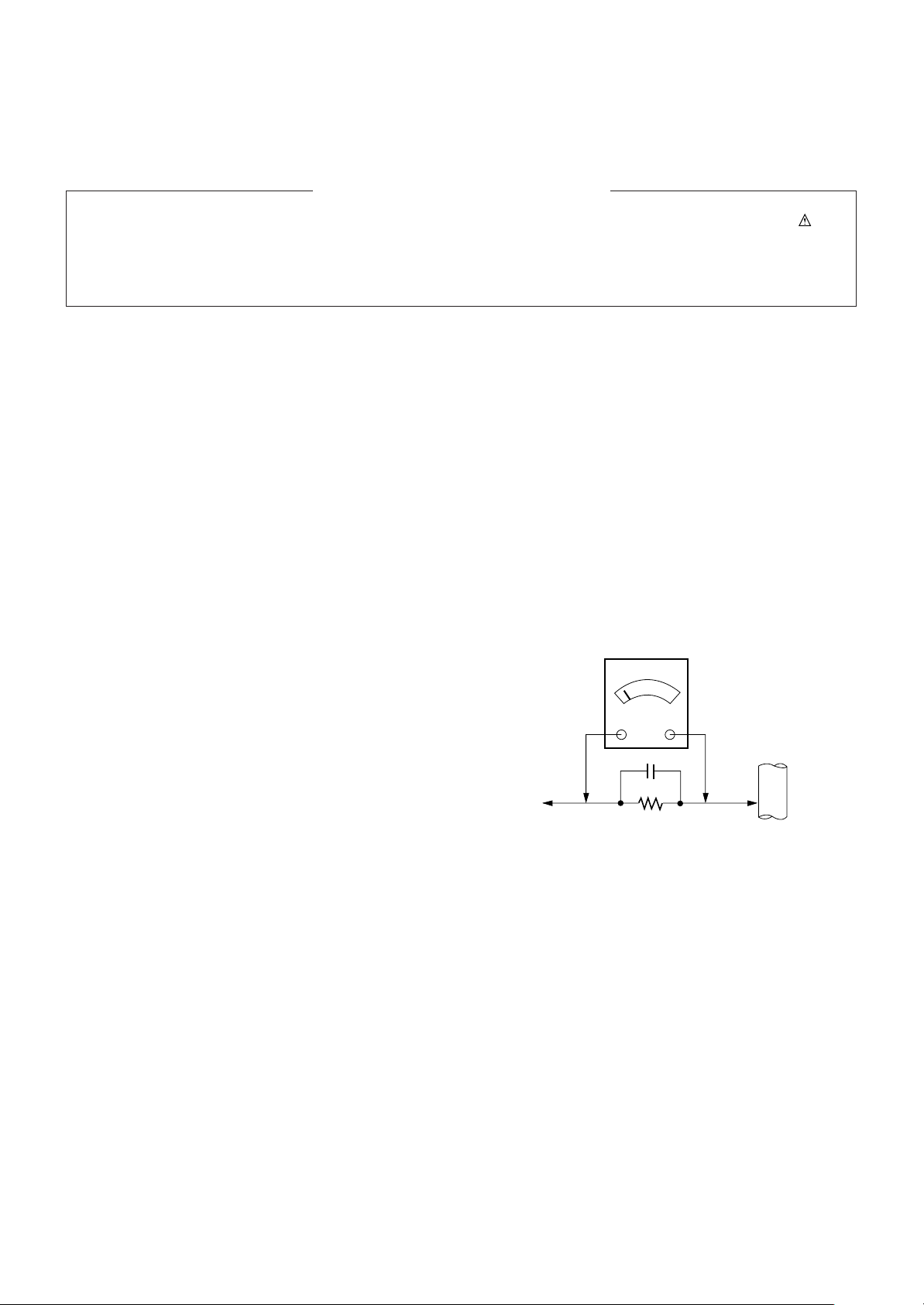
Leakage Current Hot Check (See below Figure)
Plug the AC cord directly into the AC outlet.
Do not use a line Isolation Transformer during this check.
Connect 1.5 K / 10 watt resistor in parallel with a 0.15 uF capacitor
between a known good earth ground (Water Pipe, Conduit, etc.)
and the exposed metallic parts.
Measure the AC voltage across the resistor using AC voltmeter
with 1000 ohms/volt or more sensitivity.
Reverse plug the AC cord into the AC outlet and repeat AC voltage
measurements for each exposed metallic part. Any voltage
measured must not exceed 0.75 volt RMS which is corresponds to
0.5 mA.
In case any measurement is out of the limits specified, there is
possibility of shock hazard and the set must be checked and
repaired before it is returned to the customer.
Leakage Current Hot Check circuit
1.5 Kohm/10W
To Instrument’s
exposed
METALLIC PARTS
Good Earth Ground
such as WATER PIPE,
CONDUIT etc.
AC Volt-meter
When 25A is impressed between Earth and 2nd Ground
for 1 second, Resistance must be less than 0.1
*Base on Adjustment standard
IMPORTANT SAFETY NOTICE
0.15 uF
Ω

LGE Internal Use OnlyCopyright © 2011 LG Electronics. Inc. All rights reserved.
Only for training and service purposes
- 4 -
CAUTION: Before servicing receivers covered by this service
manual and its supplements and addenda, read and follow the
SAFETY PRECAUTIONS on page 3 of this publication.
NOTE: If unforeseen circumstances create conflict between the
following servicing precautions and any of the safety precautions on
page 3 of this publication, always follow the safety precautions.
Remember: Safety First.
General Servicing Precautions
1. Always unplug the receiver AC power cord from the AC power
source before;
a. Removing or reinstalling any component, circuit board
module or any other receiver assembly.
b. Disconnecting or reconnecting any receiver electrical plug or
other electrical connection.
c. Connecting a test substitute in parallel with an electrolytic
capacitor in the receiver.
CAUTION: A wrong part substitution or incorrect polarity
installation of electrolytic capacitors may result in an
explosion hazard.
2. Test high voltage only by measuring it with an appropriate high
voltage meter or other voltage measuring device (DVM,
FETVOM, etc) equipped with a suitable high voltage probe.
Do not test high voltage by "drawing an arc".
3. Do not spray chemicals on or near this receiver or any of its
assemblies.
4. Unless specified otherwise in this service manual, clean
electrical contacts only by applying the following mixture to the
contacts with a pipe cleaner, cotton-tipped stick or comparable
non-abrasive applicator; 10 % (by volume) Acetone and 90 %
(by volume) isopropyl alcohol (90 % - 99 % strength)
CAUTION: This is a flammable mixture.
Unless specified otherwise in this service manual, lubrication of
contacts in not required.
5. Do not defeat any plug/socket B+ voltage interlocks with which
receivers covered by this service manual might be equipped.
6. Do not apply AC power to this instrument and/or any of its
electrical assemblies unless all solid-state device heat sinks are
correctly installed.
7. Always connect the test receiver ground lead to the receiver
chassis ground before connecting the test receiver positive
lead.
Always remove the test receiver ground lead last.
8. Use with this receiver only the test fixtures specified in this
service manual.
CAUTION: Do not connect the test fixture ground strap to any
heat sink in this receiver.
Electrostatically Sensitive (ES) Devices
Some semiconductor (solid-state) devices can be damaged easily
by static electricity. Such components commonly are called
Electrostatically Sensitive (ES) Devices. Examples of typical ES
devices are integrated circuits and some field-effect transistors and
semiconductor "chip" components. The following techniques
should be used to help reduce the incidence of component
damage caused by static by static electricity.
1. Immediately before handling any semiconductor component or
semiconductor-equipped assembly, drain off any electrostatic
charge on your body by touching a known earth ground.
Alternatively, obtain and wear a commercially available
discharging wrist strap device, which should be removed to
prevent potential shock reasons prior to applying power to the
unit under test.
2. After removing an electrical assembly equipped with ES
devices, place the assembly on a conductive surface such as
aluminum foil, to prevent electrostatic charge buildup or
exposure of the assembly.
3. Use only a grounded-tip soldering iron to solder or unsolder ES
devices.
4. Use only an anti-static type solder removal device. Some solder
removal devices not classified as "anti-static" can generate
electrical charges sufficient to damage ES devices.
5. Do not use freon-propelled chemicals. These can generate
electrical charges sufficient to damage ES devices.
6. Do not remove a replacement ES device from its protective
package until immediately before you are ready to install it.
(Most replacement ES devices are packaged with leads
electrically shorted together by conductive foam, aluminum foil
or comparable conductive material).
7. Immediately before removing the protective material from the
leads of a replacement ES device, touch the protective material
to the chassis or circuit assembly into which the device will be
installed.
CAUTION: Be sure no power is applied to the chassis or circuit,
and observe all other safety precautions.
8. Minimize bodily motions when handling unpackaged
replacement ES devices. (Otherwise harmless motion such as
the brushing together of your clothes fabric or the lifting of your
foot from a carpeted floor can generate static electricity
sufficient to damage an ES device.)
General Soldering Guidelines
1. Use a grounded-tip, low-wattage soldering iron and appropriate
tip size and shape that will maintain tip temperature within the
range or 500
°
F to 600 °F.
2. Use an appropriate gauge of RMA resin-core solder composed
of 60 parts tin/40 parts lead.
3. Keep the soldering iron tip clean and well tinned.
4. Thoroughly clean the surfaces to be soldered. Use a mall wirebristle (0.5 inch, or 1.25 cm) brush with a metal handle.
Do not use freon-propelled spray-on cleaners.
5. Use the following unsoldering technique
a. Allow the soldering iron tip to reach normal temperature.
(500
°F to 600 °F)
b. Heat the component lead until the solder melts.
c. Quickly draw the melted solder with an anti-static, suction-
type solder removal device or with solder braid.
CAUTION: Work quickly to avoid overheating the circuit
board printed foil.
6. Use the following soldering technique.
a. Allow the soldering iron tip to reach a normal temperature
(500
°F to 600 °F)
b. First, hold the soldering iron tip and solder the strand against
the component lead until the solder melts.
c. Quickly move the soldering iron tip to the junction of the
component lead and the printed circuit foil, and hold it there
only until the solder flows onto and around both the
component lead and the foil.
CAUTION: Work quickly to avoid overheating the circuit
board printed foil.
d. Closely inspect the solder area and remove any excess or
splashed solder with a small wire-bristle brush.
SERVICING PRECAUTIONS

LGE Internal Use OnlyCopyright © 2011 LG Electronics. Inc. All rights reserved.
Only for training and service purposes
- 5 -
IC Remove/Replacement
Some chassis circuit boards have slotted holes (oblong) through
which the IC leads are inserted and then bent flat against the
circuit foil. When holes are the slotted type, the following technique
should be used to remove and replace the IC. When working with
boards using the familiar round hole, use the standard technique
as outlined in paragraphs 5 and 6 above.
Removal
1. Desolder and straighten each IC lead in one operation by gently
prying up on the lead with the soldering iron tip as the solder
melts.
2. Draw away the melted solder with an anti-static suction-type
solder removal device (or with solder braid) before removing the
IC.
Replacement
1. Carefully insert the replacement IC in the circuit board.
2. Carefully bend each IC lead against the circuit foil pad and
solder it.
3. Clean the soldered areas with a small wire-bristle brush.
(It is not necessary to reapply acrylic coating to the areas).
"Small-Signal" Discrete Transistor
Removal/Replacement
1. Remove the defective transistor by clipping its leads as close as
possible to the component body.
2. Bend into a "U" shape the end of each of three leads remaining
on the circuit board.
3. Bend into a "U" shape the replacement transistor leads.
4. Connect the replacement transistor leads to the corresponding
leads extending from the circuit board and crimp the "U" with
long nose pliers to insure metal to metal contact then solder
each connection.
Power Output, Transistor Device
Removal/Replacement
1. Heat and remove all solder from around the transistor leads.
2. Remove the heat sink mounting screw (if so equipped).
3. Carefully remove the transistor from the heat sink of the circuit
board.
4. Insert new transistor in the circuit board.
5. Solder each transistor lead, and clip off excess lead.
6. Replace heat sink.
Diode Removal/Replacement
1. Remove defective diode by clipping its leads as close as
possible to diode body.
2. Bend the two remaining leads perpendicular y to the circuit
board.
3. Observing diode polarity, wrap each lead of the new diode
around the corresponding lead on the circuit board.
4. Securely crimp each connection and solder it.
5. Inspect (on the circuit board copper side) the solder joints of
the two "original" leads. If they are not shiny, reheat them and if
necessary, apply additional solder.
Fuse and Conventional Resistor
Removal/Replacement
1. Clip each fuse or resistor lead at top of the circuit board hollow
stake.
2. Securely crimp the leads of replacement component around
notch at stake top.
3. Solder the connections.
CAUTION: Maintain original spacing between the replaced
component and adjacent components and the circuit board to
prevent excessive component temperatures.
Circuit Board Foil Repair
Excessive heat applied to the copper foil of any printed circuit
board will weaken the adhesive that bonds the foil to the circuit
board causing the foil to separate from or "lift-off" the board. The
following guidelines and procedures should be followed whenever
this condition is encountered.
At IC Connections
To repair a defective copper pattern at IC connections use the
following procedure to install a jumper wire on the copper pattern
side of the circuit board. (Use this technique only on IC
connections).
1. Carefully remove the damaged copper pattern with a sharp
knife. (Remove only as much copper as absolutely necessary).
2. carefully scratch away the solder resist and acrylic coating (if
used) from the end of the remaining copper pattern.
3. Bend a small "U" in one end of a small gauge jumper wire and
carefully crimp it around the IC pin. Solder the IC connection.
4. Route the jumper wire along the path of the out-away copper
pattern and let it overlap the previously scraped end of the good
copper pattern. Solder the overlapped area and clip off any
excess jumper wire.
At Other Connections
Use the following technique to repair the defective copper pattern
at connections other than IC Pins. This technique involves the
installation of a jumper wire on the component side of the circuit
board.
1. Remove the defective copper pattern with a sharp knife.
Remove at least 1/4 inch of copper, to ensure that a hazardous
condition will not exist if the jumper wire opens.
2. Trace along the copper pattern from both sides of the pattern
break and locate the nearest component that is directly
connected to the affected copper pattern.
3. Connect insulated 20-gauge jumper wire from the lead of the
nearest component on one side of the pattern break to the lead
of the nearest component on the other side.
Carefully crimp and solder the connections.
CAUTION: Be sure the insulated jumper wire is dressed so the
it does not touch components or sharp edges.
LGE Internal Use OnlyCopyright © 2011 LG Electronics. Inc. All rights reserved.
Only for training and service purposes
- 6 -
SPECIFICATION
NOTE : Specifications and others are subject to change without notice for improvement
.
4. Model General Specification
1. Application range
This specification is applied to the LCD TV used LC01B
chassis.
2. Requirement for Test
Each part is tested as below without special appointment.
1) Temperature
: 25 ºC ± 5 ºC (77 ºF ± 9 ºF), CST : 40 ºC ± 5 ºC
2) Relative Humidity : 65 % ± 10 %
3) Power Voltage
: Standard input voltage (AC 100-240 V~ 50 / 60 Hz)
* Standard Voltage of each products is marked by models.
4) Specification and performance of each parts are followed
each drawing and specification by part number in
accordance with BOM.
5) The receiver must be operated for about 5 minutes prior to
the adjustment.
3. Test method
1) Performance: LGE TV test method followed
2) Demanded other specification
- Safety: CE, IEC specification
- EMC:CE, IEC
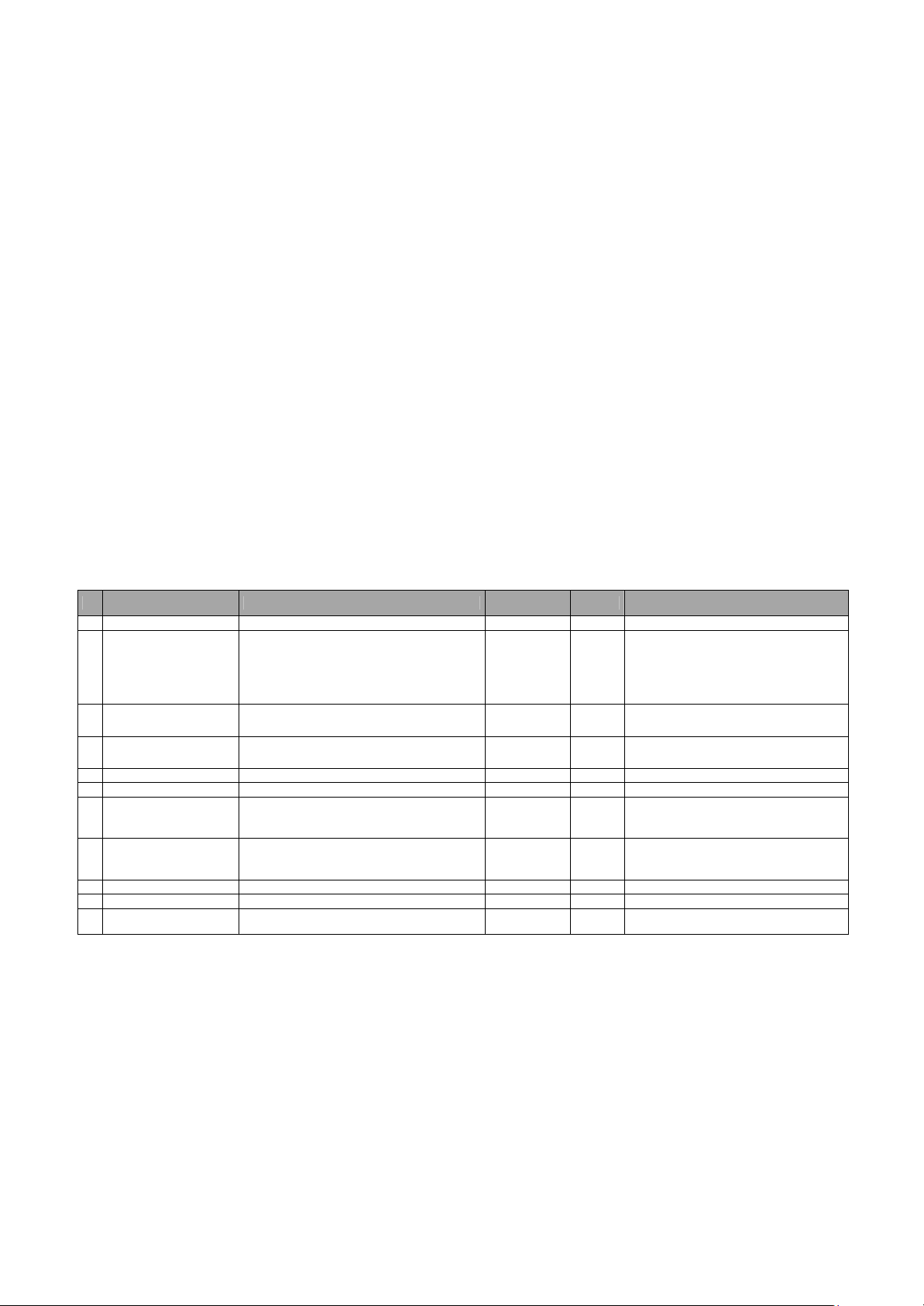
No
Item Specification Measurement Result Remarks
1 Market Hong Kong
DTV & Analog - China, Hong Kong
2 Broadcasting system
1) PAL-DK
2) PAL-I
3) NTSC-M
4) DTMB
5) DVB-C
DTMB : DMB-T 와 ADTB-T 포함
3 Receiving system
Analog : Upper Heterodyne
Digital : COFDM, QAM
4 Video Input RCA(1EA) PAL, NTSC
5 Component Input (1EA) Y/Pb/Pr
6 RGB Input RGB-PC
Analog (D-SUB 15PIN)
7 HDMI Input(3EA)
HDMI1-DTV/DVI
HDMI2-DTV (rear)
HDMI3-DTV (side)
PC(HDMI version 1.3), Support HDCP
8 Audio Input (3EA)
RGB/DVI Audio
Component(1EA)
AV(1EA)
L/R Input
9 SDPIF out (1EA) SPDIF out
Rear
10. Earphone out (1EA)
Side
l11 USB (1EA) Divx(HD), EMF(JPEG, MP3), SVC(download)
Side
- 7 -
LGE Internal Use OnlyCopyright © 2011 LG Electronics. Inc. All rights reserved.
Only for training and service purposes
5. Component Video Input (Y, PB, PR)
No.
Specification
Remark
Resolution H-freq(kHz) V-freq(Hz)
1. 720x480 15.73 60.00 SDTV,DVD 480i
2. 720x480 15.63 59.94 SDTV,DVD 480i
3. 720x480 31.47 59.94 480p
4. 720x480 31.50 60.00 480p
5. 720x576 15.625 50.00 SDTV,DVD 625 Line
6. 720x576 31.25 50.00 HDTV 576p
7. 1280x720 45.00 50.00 HDTV 720p
8. 1280x720 44.96 59.94 HDTV 720p
9. 1280x720 45.00 60.00 HDTV 720p
10. 1920x1080 31.25 50.00 HDTV 1080i
11. 1920x1080 33.75 60.00 HDTV 1080i
12. 1920x1080 33.72 59.94 HDTV 1080i
13. 1920x1080 56.250 50 HDTV 1080p
14. 1920x1080 67.5 60 HDTV 1080p
6. RGB Input (PC)
No Resolution H-freq(kHz) V-freq.(Hz) Pixel clock (MHz)
Proposed Remarks
1. 720*400 31.468 70.08 28.321 For only DOS mode
2. 640*480 31.469 59.94 25.17 VESA
Input 848*480 60Hz, 852*480 60Hz
640*480 60Hz Display
3. 800*600
37.879
60.31 40.00 VESA
4. 1024*768 48.363 60.00 65.00 VESA(XGA)
5. 1280*768 47.78 59.87 79.5 WXGA
6. 1360*768 47.72 59.8 84.75 WXGA FHD model
7. 1366*768 47.56 59.6 84.75 WXGA WXGA model
8. 1280*1024 63.595 60.0 108.875 SXGA FHD model
9. 1280*720 45 60 74.25 720P DTV standard
10. 1920*1080 66.587 59.93 138.5 WUXGA FHD model
- 8 -
LGE Internal Use OnlyCopyright © 2011 LG Electronics. Inc. All rights reserved.
Only for training and service purposes
7. HDMI Input
(1) DTV Mode
No. Resolution H-freq(kHz) V-freq.(Hz) Pixel clock(MHz) Proposed Remark
1. 720*400 31.468 70.08 28.321 HDCP
2. 640*480 31.469 59.94 25.17 VESA HDCP
3. 800*600 37.879 60.31 40.00 VESA HDCP
4. 1024*768 48.363 60.00 65.00 VESA(XGA) HDCP
5. 1360*768 47.72 59.8 84.75 WXGA HDCP
6. 1280*1024 63.981 60.02 108.875 SXGA HDCP/FHD model
7. 1920*1080 67.5 60.00 138.625 WUXGA HDCP/FHD model
(2) PC Mode
No. Resolution H-freq(kHz) V-freq.(Hz) Pixel clock(MHz) Proposed Remark
1. 720*480 31.469 /31.5 59.94 /60 27.00/27.03 SDTV 480P
2. 720*576 31.25 50 54 SDTV 576P
3. 1280*720 37.500 50 74.25 HDTV 720P
4. 1280*720 44.96 /45 59.94 /60 74.17/74.25 HDTV 720P
5. 1920*1080 33.72 /33.75 59.94 /60 74.17/74.25 HDTV 1080I
6. 1920*1080 28.125 50.00 74.25 HDTV 1080I
7. 1920*1080 26.97 /27 23.97 /24 74.17/74.25 HDTV 1080P
8. 1920*1080 33.716 /33.75 29.976 /30.00 74.25 HDTV 1080P
9. 1920*1080 56.250 50 148.5 HDTV 1080P
10. 1920*1080 67.43 /67.5 59.94 /60 148.35/148.50 HDTV 1080P
LGE Internal Use OnlyCopyright © 2011 LG Electronics. Inc. All rights reserved.
Only for training and service purposes
- 9 -
ADJUSTMENT INSTRUCTION
1. Application Range
This specification sheet is applied to all of the LCD TV with
LC01T chassis.
2. Designation
1) The adjustment is according to the order which is designated
and which must be followed, according to the plan which can
be changed only on agreeing.
2) Power Adjustment: Free Voltage
3) Magnetic Field Condition: Nil.
4) Input signal Unit: Product Specification Standard
5) Reserve after operation: Above 5 Minutes (Heat Run)
Temperature : at 25 ºC ± 5 ºC
Relative humidity : 65 % ± 10 %
Input voltage : 220 V, 60 Hz
6) Adjustment equipments: Color Analyzer(CA-210 or CA-110),
DDC Adjustment Jig equipment, Service remote control.
7) Push the “IN STOP” key - For memory initialization.
3. Main PCB check process
* APC - After Manual-Insert, executing APC
* Boot file Download
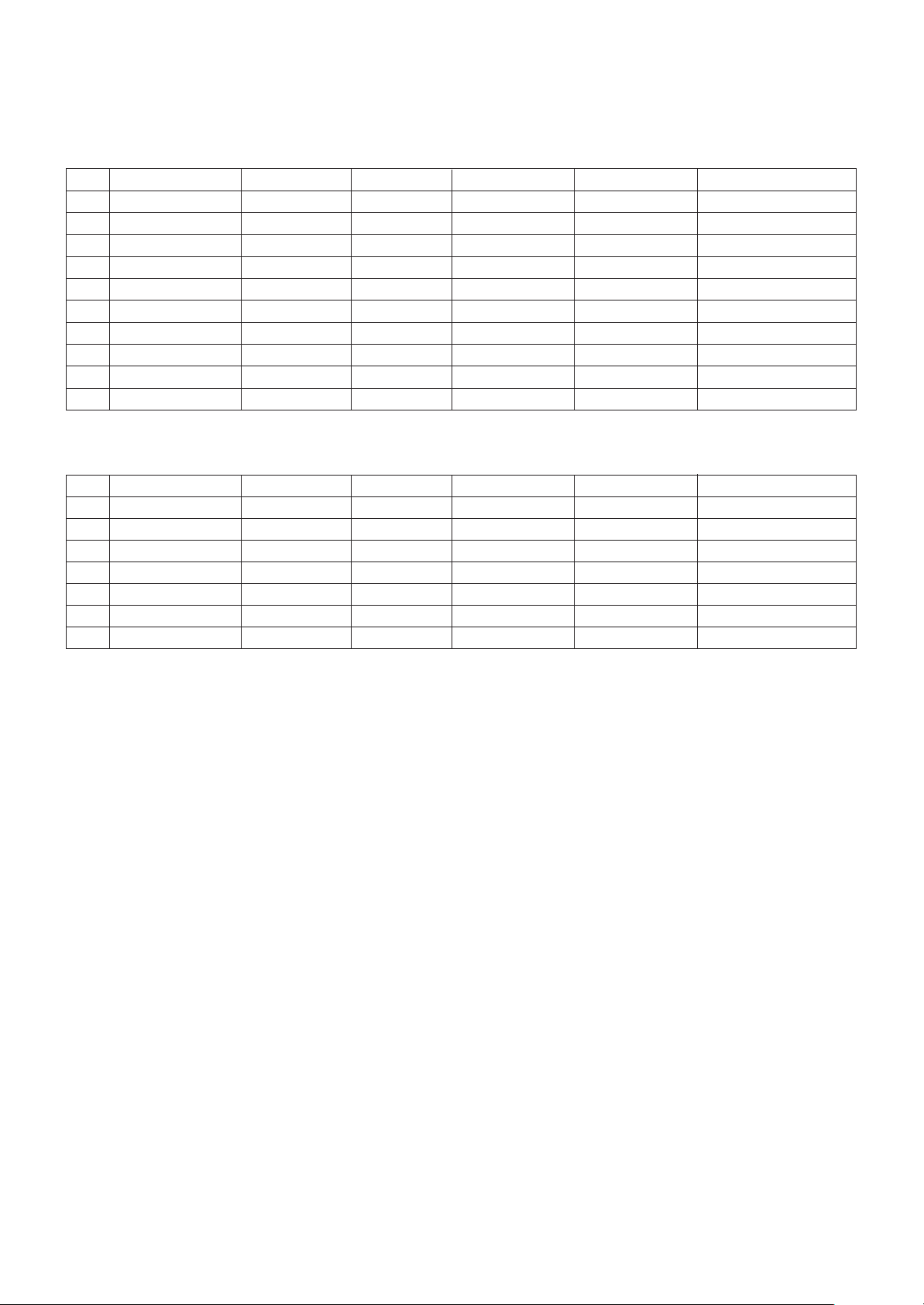
1) Execute ISP program “Mstar ISP Utility” and then click
“Config” tab.
2) Set as below, and then click “Auto Detect” and check “OK”
message
If “Error” is displayed, Check connection between
computer, jig, and set.
3) Click “Read” tab, and then load download file (XXXX.bin)
by clicking “Read”
4) Click “Connect” tab. If “Can’t” is displayed, check
connection between computer, jig, and set.
5) Click “Auto” tab and set as below.
6) Click “Run”.
7) After downloading, check “OK” message.
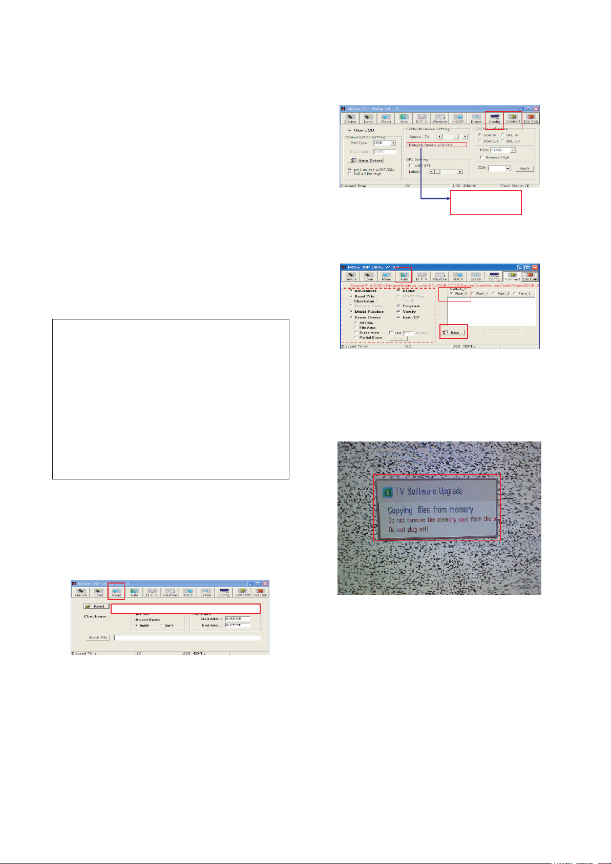
* USB DOWNLOAD
1) Put the USB Stick to the USB socket.
2) Automatically detecting update file in USB Stick.
- If your downloaded program version in USB Stick is Low,
it didn’t work. But your downloaded version is High, USB
data is automatically detecting.
3) Show the message “Copying files from memory”.
filexxx.bin
(4)
(7) .OK
(5)
(6)
(1)
fil exxx.bi n
(2)
(3)
Please Check the Speed :
To use speed between
from 200KHz to 400KHz
Case1 : Software version up
1. After downloading S/W by USB, TV set will reboot
automatically
2. Push “In-stop” key
3. Push “Power on” key
4. Function inspection
5. After function inspection, Push “In-stop” key.
Case2 : Function check at the assembly line
1. When TV set is entering on the assembly line, Push
“In-stop” key at first.
2. Push “Power on” key for turning it on.
-> If you push “Power on” key, TV set will recover
channel information by itself.
3. After function inspection, Push “In-stop” key.
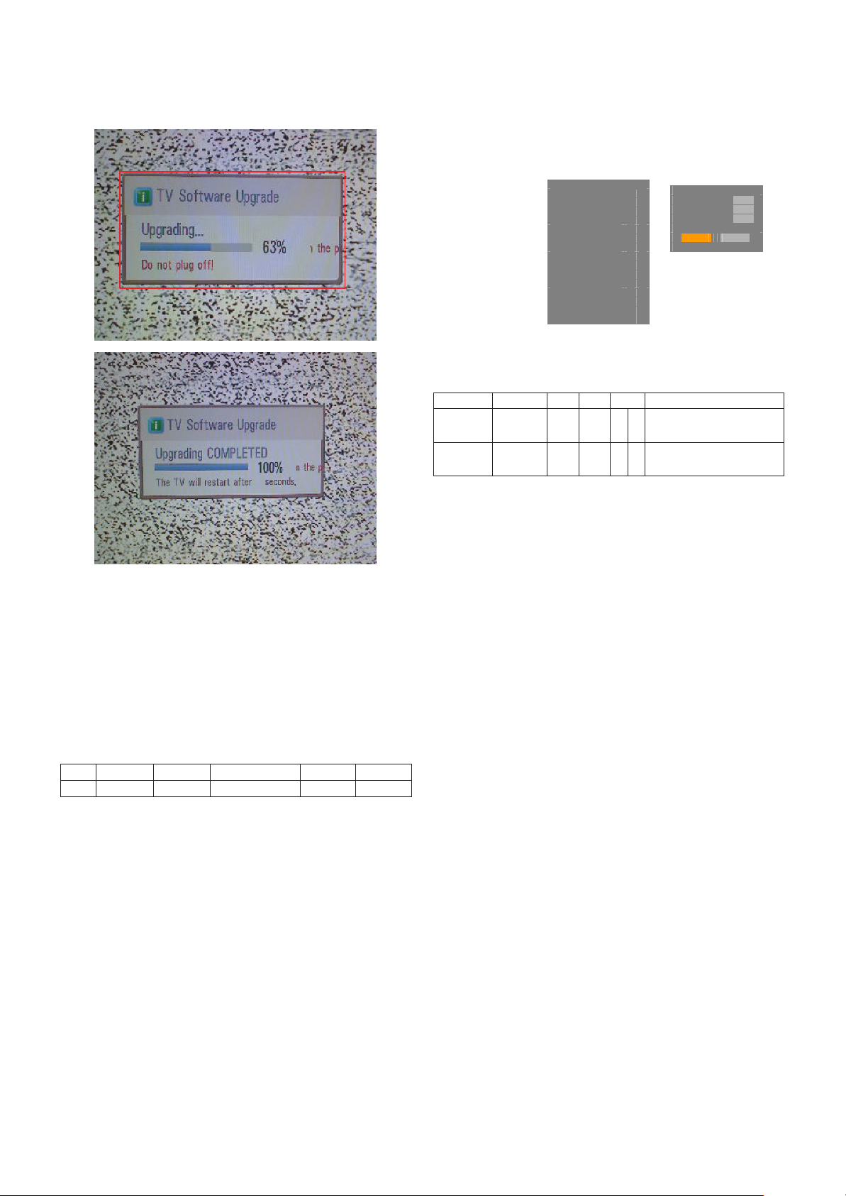
4) Updating is starting.
5) Uploading completed, The TV will restart automatically.
6) If your TV is turned on, check your updated version and
Tool option.(explain the Tool option, next stage)
* If downloading version is more high than your TV have,
TV can lost all channel data. In this case, you have to
channel recover. if all channel data is cleared, you didn’t
have a DTV/ATV test on production line.
* After downloading, have to adjust Tool Option again.
1) Push "IN-START" key in service remote control.
2) Select “Tool Option 1” and Push “OK” key.
3) Punch in the number. (Each model has their number)
4) Completed selecting Tool option.
3.1. ADC Process
(1) ADC
- Enter Service Mode by pushing “ADJ” key,
- Enter Internal ADC mode by pushing “
G
” key at “5. ADC
Calibration”
<Caution> Using ‘power on’ button of the Adjustment remote
control, power on TV.
* ADC Calibration Protocol (RS232)
Adjust Sequence
• aa 00 00 [Enter Adjust Mode]
• xb 00 40 [Component1 Input (480i)]
• ad 00 10 [Adjust 480i Comp1]
• xb 00 60 [RGB Input (1024*768)]
• ad 00 10 [Adjust 1024*768 RGB]
• aa 00 90 End Adjust mode
* Required equipment : Adjustment remote control.
3.2. Function Check
* Check display and sound
- Check Input and Signal items. (cf. work instructions)
1) TV
2) AV (SCART1/SCART2/ CVBS)
3) COMPONENT (480i)
4) RGB (PC : 1024 x 768 @ 60 hz)
5) HDMI
6) PC Audio In
* Display and Sound check is executed by Remote control.
- 10 -
LGE Internal Use OnlyCopyright © 2011 LG Electronics. Inc. All rights reserved.
Only for training and service purposes
No Item CMD1 CMD2 Data0
Enter Adjust Adjust A A 0 0 When transfer the ‘Mode In’,
Mode ‘Mode In’ Carry the command.
ADC adjust ADC Adjust A D 1 0 Automatically adjustment
(The use of a internal pattern)
Module Tool option1 Tool option2 Tool option3(AU,TS) Tool option4 Tool option5
CMI 10020 8726 55337 26904 288
ADC Calib ration
ADC Comp 480i NG
ADC Comp 1080p NG
ADC RGB N G
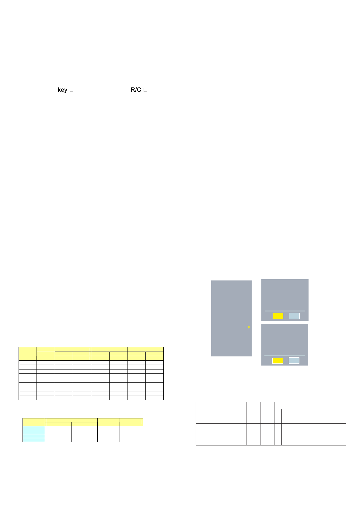
Start Reset
EZ ADJUST
0. Tool Optio n1
1. Tool Optio n2
2. Tool Optio n3
3. Tool Optio n4
4. Tool Optio n5
5. Country Gr oup
6. ADC Cal ibration ▶
7. White Bal ance
8. 10 Point WB
9. Test Patt ern
10. EDID D/L
11. Sub B/C
12. V-Com
13. P-Gamm a
- 11 -
LGE Internal Use OnlyCopyright © 2011 LG Electronics. Inc. All rights reserved.
Only for training and service purposes
4. White Balance Adjustment
4.1 Overview
▪ W/B adj. Objective & How-it-works
- Objective: To reduce each Panel’s W/B deviation
- How-it-works: When R/G/B gain in the OSD is at
192, it means the panel is at its Full Dynamic Range. In order to prevent saturation of Full Dynamic
range and data, one of R/G/B is fixed at 192, and
the other two is lowered to find the desired value.
-Adj. condition : normal temperature
1) Surrounding Temperature: 25±5
2) Warm-up time: About 5 Min
3) Surrounding Humidity: 20% ~ 80%
4. 2 Equipment
1) Color Analyzer: CA-210 (LED Module : CH 14)
2) Adj. Computer(During auto adj., RS-232C protocol is
needed)
3) Adjust Remocon 4) Video Signal Generator MSPG925F 720p/216-Gray(Model:217, Pattern:78)
→ Only when internal pattern is not available
▪Color Analyzer Matrix should be calibrated using CS
-1000
4.3 Equipment connection MAP
RS-232C COMMAND
[CMD ID DATA]
Explanation
wb 00 00 Begin White Balance adj.
wb 00 10 Gain adj.(internal white pattern)
wb 00 1f Gain adj. completed
wb 00 20 Offset adj.(internal white pattern)
wb 00 2f Offset adj. completed
wb 00 ff End White Balance adj.
(internal pattern disappears )
Ex) wb 00 00 -> Begin white balance auto-adj.
wb 00 10 -> Gain adj.
ja 00 ff -> Adj. data
jb 00 c0
...
...
4.4 Adj. Command (Protocol)
<Command Format>
START 6E A 50 A LEN A 03 A CMD
A 00 A VAL A CS A STOP
- LEN: Number of Data Byte to be sent
- CMD: Command
- VAL: FOS Data value
- CS: Checksum of sent data
- A: Acknowledge
Ex) [Send: JA_00_DD] / [Ack: A_00_okDDX]
▪ RS-232C Command used during auto-adj.
4.5 Adj. method
4.5.1 Auto adj. method
1) Set TV in adj. mode using POWER ON key
2) Zero calibrate probe then place it on the center of the
Display.
3) Connect Cable(RS-232C).
4) Select mode in adj. Program and begin adj.
5) When adj. is complete (OK Sing), check adj. status pre
mode (Warm, Medium, Cool) 6) Remove probe and RS232C cable to complete adj.
▪ W/B Adj. must begin as start command “wb 00 00” , and
finish as end command “wb 00 ff”, and Adj. offset if need .
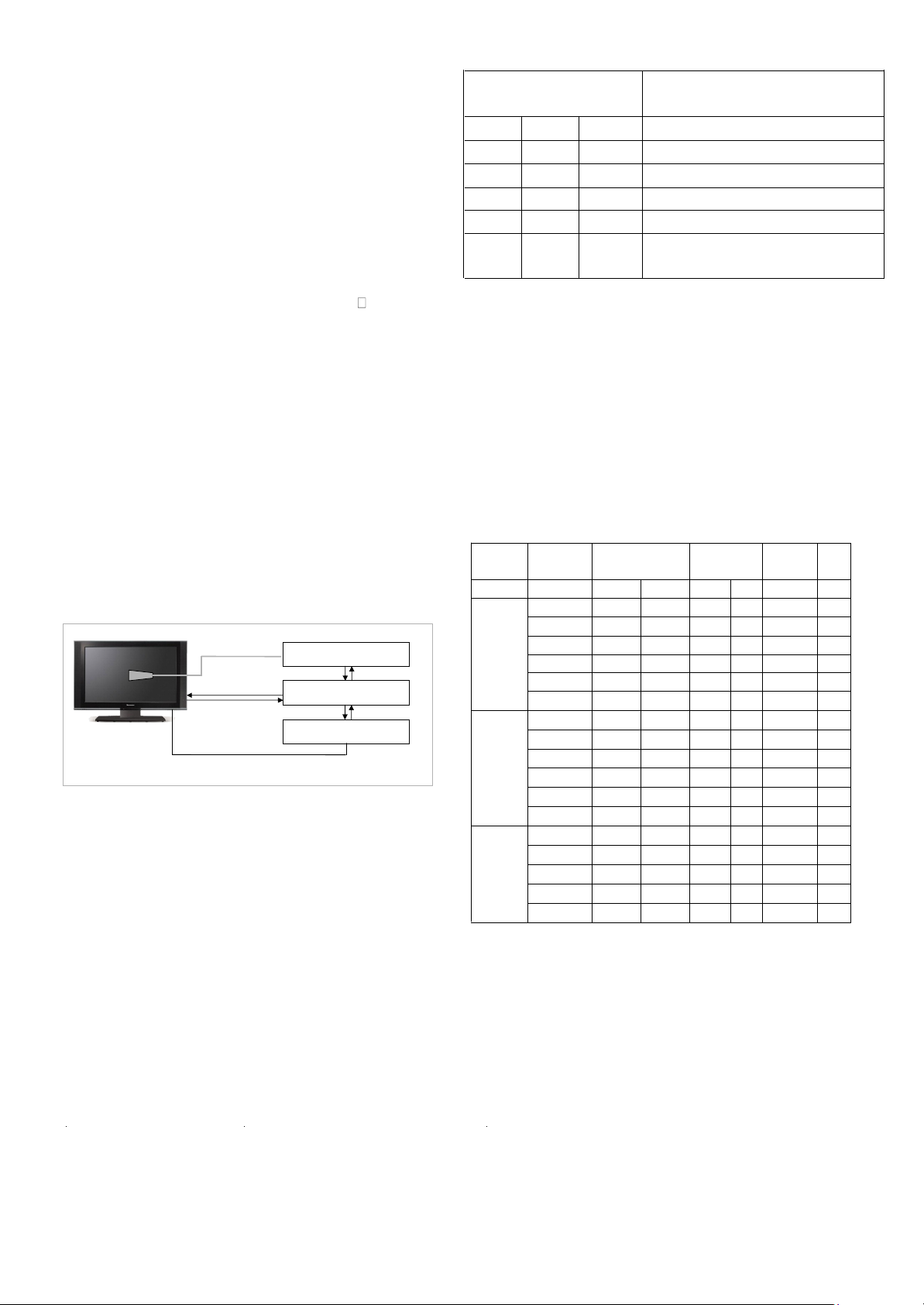
Color Analyzer
Probe
RS-
232C
Signal Source
※If TV internal pattern is used, not
※
Pattern Generator
Comput er
RS-
232C
RS-
232C
wb 00 1f -> Gain adj. complete
*(wb 00 20(start), wb 00 2f(endc)) -> Off-set adj.
wb 00 ff ->End white balance auto adj.
▪Adj. Map
Adj. item Command
(lower caseASCII)
CMD1 CMD2 MIN MAX
Cool
Medium
Warm
R Gain j g 00 C0 TBD
G Gain j h 00 C0 TBD
B Gain j i 00 C0 TBD
R Cut TBD
G Cut TBD
B Cut TBD
R Gain j a 00 C0 TBD
G Gain j b 00 C0 TBD
B Gain j c 00 C0 TBD
R Cut TBD
G Cut TBD
B Cut TBD
R Gain j d 00 C0 TBD
G Gain j e 00 C0 TBD
B Gain j f 00 C0 TBD
R Cut TBD
G Cut TBD
Data Range
(Hex.)
Default
(Decimal)
Details
LGE Internal Use OnlyCopyright © 2011 LG Electronics. Inc. All rights reserved.
Only for training and service purposes
- 12 -
4.5. EDID DATA
1) All Data : HEXA Value
2) Changeable Data :
*: Serial No : Controlled / Data:01
**: Month : Controlled / Data:00
4.6. Auto Download
1) After ener Service Mode by pushing “ADJ” key.
2) Enter EDID D/L menu.
3) Enter “START” by pushing “OK” key.
<Caution> Nerver connect HDMI && D-sub cable when EDID
downloaded
* Edid data and Model option download (RS232)
EZ ADJUT
0. Tool Option1
1. Tool Option2
2. Tool Option3
3. Tool Option4
4. Country Group
5. ADC Calibration
6. White Balance
7. Test Pattern
8. EDID D/L
9. Sub B/C
10. V-Com
11. P-Gamma
EDID D/L
HDMI1
HDMI2
HDMI3
RGB
NG
NG
NG
NG
Reset
Start
EDID D/L
Reset
Start
HDMI1
HDMI2
HDMI3
RGB
OK
OK
OK
OK
NO Item CMD1 CMD2 Data0
Enter Download A A 0 0 When transfer the ‘Mode In’,
download Mode ‘Mode In’ Carry the command.
EDID data and Download A E 00 10 Automatically Download
Model option (The use of a internal pattern)
download
4.5.2 Manual adj. method
1) Set TV in Adj. mode using POWER ON
2) Zero Calibrate the probe of Color Analyzer, then place
it on the center of LCD module within 10cm of the surface.
3) Press ADJ
Balance then press the cursor to the right (KEY). (When KEY() is pressed 216 Gray internal pattern will be displayed)
4) One of R Gain / G Gain / B Gain should be fixed at 192,
and the rest will be lowered to meet the desired value.
5) Adj. is performed in COOL, MEDIUM, WARM
color temperature.
▪ If internal pattern is not available, use RF input. In EZ
Adj. menu 7.White Balance, you can select one of 2
Testpattern: ON, OFF. Default is inner(ON). By selecting
OFF, you can adjust using RF signal in 216 Gray pattern.
Adj. condition and cautionary items
▪
1) Lighting condition in surrounding area
Surrounding lighting should be lower 10 lux. Try to
isolate adj. area into dark surrounding.
2) Probe location
- PDP: Color Analyzer (CA-100, CA-100+, CA210)
probe should be fi
- LCD: Color Analyzer (CA-210) probe should be within
10cm and perpendicular of the module surface (80°~
100°)
3) Aging time
- After Aging Start, Keep the Power ON status during
5 Minutes.
- In case of LCD, Back-light on should be checked using
no signal or Fu
4.6 Reference (White Balance Adj. coordinate
and color temperature)
▪ Luminance: 216 Gray
[ Color Temperature ]
▪ LGD Edge LED Models
Aging time Cool(13000k) Medium(9500k) Warm(6500k)
GP3
(Min)
0-2
1
2
3-5
3
6-9
4
10-19
20-35
5
36-49
6
50-79
7
80-149
8
Over 150
9
▪ O/S Edge LED Models
Mode
Medium 0.285(±0.002) 0.293(±0.002) 9300K 0.0000
0.276(±0.002) 0.283(±0.002
Cool
Warm 0.313(±0.002) 0.329(±0.002) 6500K 0.0000
EZ adjust using adj. 7. White-
3 modes of
rmly attached to the Module
ll-white pattern.
X(±0.002) y(±0.002) x(±0.002) y(±0.002) x(±0.002) y(±0.002)
269 273 285 293 313 329
279 288 295 308 319 338
278 286 294 306 318 336
277 285 293 305 317 335
276 283 292 303 316 333
274 280 290 300 314 330
272 277 288 297 312 327
271 275 287 295 311 325
270 274 286 294 310 324
269 273 285 293 309 323
Coordinate
x y
)
Temp △uv
11000K 0.0000
4.3 DDC EDID Write (RGB 128Byte )
■ Connect D-sub Signal Cable to D-Sub Jack.
■ Write EDID DATA to EEPROM (24C02) by using DDC2B
protocol.
■ Check whether written EDID data is correct or not.
* For SVC main Ass’y, EDID have to be downloaded to
Insert Process in advance.
4.4 DDC EDID Write (HDMI 256Byte)
■ Connect HDMI Signal Cable to HDMI Jack.
■ Write EDID DATA to EEPROM(24C02) by using DDC2B
protocol.
■ Check whether written EDID data is correct or not.
* For SVC main Ass’y, EDID have to be downloaded to
Insert Process in advance.
 Loading...