

Page 1

Internal Use Only
North/Latin America http://aic.lgservice.com
Europe/Africa http://eic.lgservice.com
Asia/Oceania http://biz.lgservice.com
LED TV
SERVICE MANUAL
CHASSIS : LJ31A / LD31T
MODEL : 26LN45** 26LN45**-T*
CAUTION
BEFORE SERVICING THE CHASSIS,
READ THE SAFETY PRECAUTIONS IN THIS MANUAL.
Printed in KoreaP/NO : MFL67739001 (1303-REV00)
Page 2

CONTENTS
CONTENTS .............................................................................................. 2
SAFETY PRECAUTIONS ........................................................................ 3
SERVICING PRECAUTIONS ................................................................... 4
SPECIFICATION ...................................................................................... 6
ADJUSTMENT INSTRUCTION ............................................................... 9
TROUBLE SHOOTING .......................................................................... 13
BLOCK DIAGRAM ................................................................................. 17
EXPLODED VIEW .................................................................................. 18
SCHEMATIC CIRCUIT DIAGRAM ..............................................................
Only for training and service purposes
- 2 -
LGE Internal Use OnlyCopyright © LG Electronics. Inc. All rights reserved.
Page 3
SAFETY PRECAUTIONS
IMPORTANT SAFETY NOTICE
Many electrical and mechanical parts in this chassis have special safety-related characteristics. These parts are identified by in the
Schematic Diagram and Exploded View.
It is essential that these special safety parts should be replaced with the same components as recommended in this manual to prevent
Shock, Fire, or other Hazards.
Do not modify the original design without permission of manufacturer.
General Guidance
An isolation Transformer should always be used during the
servicing of a receiver whose chassis is not isolated from the AC
power line. Use a transformer of adequate power rating as this
protects the technician from accidents resulting in personal injury
from electrical shocks.
It will also protect the receiver and it's components from being
damaged by accidental shorts of th e cir cuitry that may be
inadvertently introduced during the service operation.
If any fuse (or Fusible Resistor) in this TV receiver is blown,
replace it with the specified.
When replacing a high wattage resistor (Oxide Metal Film Resistor,
over 1 W), keep the resistor 10 mm away from PCB.
Keep wires away from high voltage or high temperature parts.
Before returning the receiver to the customer,
always perform an AC leakage current check on the exposed
metallic parts of the cabinet, such as antennas, terminals, etc., to
be sure the set is safe to operate without damage of electrical
shock.
Leakage Current Cold Check(Antenna Cold Check)
With the instrument AC plug removed from AC source, connect an
electrical jumper across the two AC plug prongs. Place the AC
switch in the on position, connect one lead of ohm-meter to the AC
plug prongs tied together and touch other ohm-meter lead in turn to
each exposed metallic parts such as antenna terminals, phone
jacks, etc.
If the exposed metallic part has a return path to the chassis, the
measured resistance should be between 1 MΩ and 5.2 MΩ.
When the exposed metal has no return path to the chassis the
reading must be infinite.
An other abnormality exists that must be corrected before the
receiver is returned to the customer.
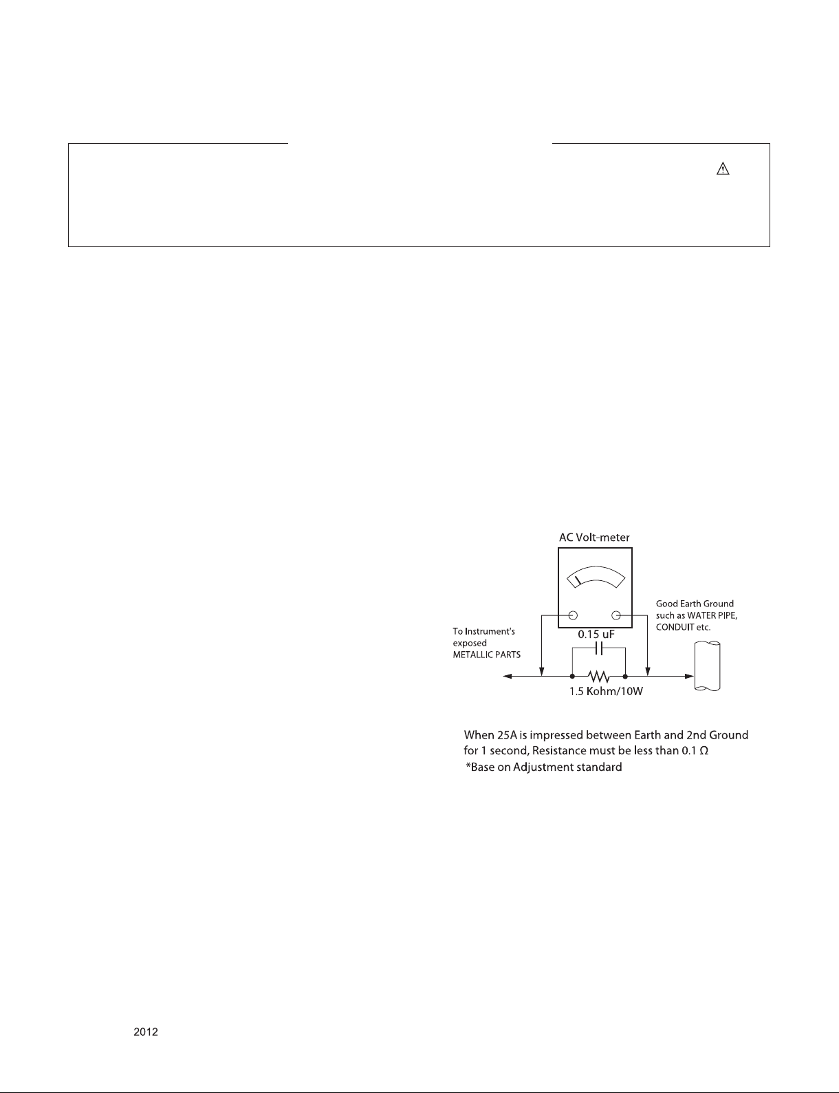
Leakage Current Hot Check (See below Figure)
Plug the AC cord directly into the AC outlet.
Do not use a line Isolation Transformer during this check.
Connect 1.5 K / 10 watt resistor in parallel with a 0.15 uF capacitor
between a known good earth ground (Water Pipe, Conduit, etc.)
and the exposed metallic parts.
Measure the AC voltage across the resistor using AC voltmeter
with 1000 ohms/volt or more sensitivity.
Reverse plug the AC cord into the AC outlet and repeat AC voltage
measurements for each exp ose d metallic par t. Any voltage
measured must not exceed 0.75 volt RMS which is corresponds to
0.5 mA.
In case any measurement is out of the limits specified, there is
possibility of shock hazard and the set must be checked and
repaired before it is returned to the customer.
Leakage Current Hot Check circuit
Only for training and service purposes
- 3 -
LGE Internal Use OnlyCopyright © LG Electronics. Inc. All rights reserved.
Page 4

SERVICING PRECAUTIONS
CAUTION: Before servicing receivers covered by this service
manual and its supplements and addenda, read and follow the
SAFETY PRECAUTIONS on page 3 of this publication.
NOTE: If unforeseen circumstances create conict between the
following servicing precautions and any of the safety precautions
on page 3 of this publication, always follow the safety precautions. Remember: Safety First.
General Servicing Precautions
1. Always unplug the receiver AC power cord from the AC power
source before;
a. Removing or reinstalling any component, circuit board
module or any other receiver assembly.
b. Disconnecting or reconnecting any receiver electrical plug
or other electrical connection.
c. Connecting a test substitute in parallel with an electrolytic
capacitor in the receiver.
CAUTION: A wrong part substitution or incorrect polarity
installation of electrolytic capacitors may result in an explosion hazard.
2. Test high voltage only by measuring it with an appropriate
high voltage meter or other voltage measuring device (DVM,
FETVOM, etc) equipped with a suitable high voltage probe.
Do not test high voltage by "drawing an arc".
3. Do not spray chemicals on or near this receiver or any of its
assemblies.
4. Unless specied otherwise in this service manual, clean
electrical contacts only by applying the following mixture to the
contacts with a pipe cleaner, cotton-tipped stick or comparable
non-abrasive applicator; 10 % (by volume) Acetone and 90 %
(by volume) isopropyl alcohol (90 % - 99 % strength)
CAUTION: This is a ammable mixture.
Unless specied otherwise in this service manual, lubrication
of contacts in not required.
5. Do not defeat any plug/socket B+ voltage interlocks with which
receivers covered by this service manual might be equipped.
6. Do not apply AC power to this instrument and/or any of its
electrical assemblies unless all solid-state device heat sinks
are correctly installed.
7. Always connect the test receiver ground lead to the receiver
chassis ground before connecting the test receiver positive
lead.
Always remove the test receiver ground lead last.
8. Use with this receiver only the test xtures specied in this
service manual.
CAUTION: Do not connect the test xture ground strap to any
heat sink in this receiver.
Electrostatically Sensitive (ES) Devices
Some semiconductor (solid-state) devices can be damaged easily by static electricity. Such components commonly are called
Electrostatically Sensitive (ES) Devices. Examples of typical ES
devices are integrated circuits and some eld-effect transistors
and semiconductor “chip” components. The following techniques
should be used to help reduce the incidence of component damage caused by static by static electricity.
1. Immediately before handling any semiconductor component or
semiconductor-equipped assembly, drain off any electrostatic
charge on your body by touching a known earth ground. Alternatively, obtain and wear a commercially available discharging wrist strap device, which should be removed to prevent
potential shock reasons prior to applying power to the unit
under test.
2. After removing an electrical assembly equipped with ES
devices, place the assembly on a conductive surface such as
aluminum foil, to prevent electrostatic charge buildup or exposure of the assembly.
3. Use only a grounded-tip soldering iron to solder or unsolder
ES devices.
4. Use only an anti-static type solder removal device. Some solder removal devices not classied as “anti-static” can generate
electrical charges sufcient to damage ES devices.
5. Do not use freon-propelled chemicals. These can generate
electrical charges sufcient to damage ES devices.
6. Do not remove a replacement ES device from its protective
package until immediately before you are ready to install it.
(Most replacement ES devices are packaged with leads electrically shorted together by conductive foam, aluminum foil or
comparable conductive material).
7. Immediately before removing the protective material from the
leads of a replacement ES device, touch the protective material to the chassis or circuit assembly into which the device will
be installed.
CAUTION: Be sure no power is applied to the chassis or circuit, and observe all other safety precautions.
8. Minimize bodily motions when handling unpackaged replacement ES devices. (Otherwise harmless motion such as the
brushing together of your clothes fabric or the lifting of your
foot from a carpeted oor can generate static electricity sufcient to damage an ES device.)
General Soldering Guidelines
1. Use a grounded-tip, low-wattage soldering iron and appropriate tip size and shape that will maintain tip temperature within
the range or 500 °F to 600 °F.
2. Use an appropriate gauge of RMA resin-core solder composed
of 60 parts tin/40 parts lead.
3. Keep the soldering iron tip clean and well tinned.
4. Thoroughly clean the surfaces to be soldered. Use a mall wirebristle (0.5 inch, or 1.25 cm) brush with a metal handle.
Do not use freon-propelled spray-on cleaners.
5. Use the following unsoldering technique
a. Allow the soldering iron tip to reach normal temperature.
(500 °F to 600 °F)
b. Heat the component lead until the solder melts.
c. Quickly draw the melted solder with an anti-static, suction-
type solder removal device or with solder braid.
CAUTION: Work quickly to avoid overheating the circuit
board printed foil.
6. Use the following soldering technique.
a. Allow the soldering iron tip to reach a normal temperature
(500 °F to 600 °F)
b. First, hold the soldering iron tip and solder the strand
against the component lead until the solder melts.
c. Quickly move the soldering iron tip to the junction of the
component lead and the printed circuit foil, and hold it there
only until the solder ows onto and around both the component lead and the foil.
CAUTION: Work quickly to avoid overheating the circuit
board printed foil.
d. Closely inspect the solder area and remove any excess or
splashed solder with a small wire-bristle brush.
Only for training and service purposes
- 4 -
LGE Internal Use OnlyCopyright © LG Electronics. Inc. All rights reserved.
Page 5

IC Remove/Replacement
Some chassis circuit boards have slotted holes (oblong) through
which the IC leads are inserted and then bent at against the circuit foil. When holes are the slotted type, the following technique
should be used to remove and replace the IC. When working with
boards using the familiar round hole, use the standard technique
as outlined in paragraphs 5 and 6 above.
Removal
1. Desolder and straighten each IC lead in one operation by
gently prying up on the lead with the soldering iron tip as the
solder melts.
2. Draw away the melted solder with an anti-static suction-type
solder removal device (or with solder braid) before removing
the IC.
Replacement
1. Carefully insert the replacement IC in the circuit board.
2. Carefully bend each IC lead against the circuit foil pad and
solder it.
3. Clean the soldered areas with a small wire-bristle brush.
(It is not necessary to reapply acrylic coating to the areas).
"Small-Signal" Discrete Transistor
Removal/Replacement
1. Remove the defective transistor by clipping its leads as close
as possible to the component body.
2. Bend into a "U" shape the end of each of three leads remaining on the circuit board.
3. Bend into a "U" shape the replacement transistor leads.
4. Connect the replacement transistor leads to the corresponding
leads extending from the circuit board and crimp the "U" with
long nose pliers to insure metal to metal contact then solder
each connection.
Power Output, Transistor Device
Removal/Replacement
1. Heat and remove all solder from around the transistor leads.
2. Remove the heat sink mounting screw (if so equipped).
3. Carefully remove the transistor from the heat sink of the circuit
board.
4. Insert new transistor in the circuit board.
5. Solder each transistor lead, and clip off excess lead.
6. Replace heat sink.
Diode Removal/Replacement
1. Remove defective diode by clipping its leads as close as possible to diode body.
2. Bend the two remaining leads perpendicular y to the circuit
board.
3. Observing diode polarity, wrap each lead of the new diode
around the corresponding lead on the circuit board.
4. Securely crimp each connection and solder it.
5. Inspect (on the circuit board copper side) the solder joints of
the two "original" leads. If they are not shiny, reheat them and
if necessary, apply additional solder.
3. Solder the connections.
CAUTION: Maintain original spacing between the replaced
component and adjacent components and the circuit board to
prevent excessive component temperatures.
Circuit Board Foil Repair
Excessive heat applied to the copper foil of any printed circuit
board will weaken the adhesive that bonds the foil to the circuit
board causing the foil to separate from or "lift-off" the board. The
following guidelines and procedures should be followed whenever this condition is encountered.
At IC Connections
To repair a defective copper pattern at IC connections use the
following procedure to install a jumper wire on the copper pattern
side of the circuit board. (Use this technique only on IC connections).
1. Carefully remove the damaged copper pattern with a sharp
knife. (Remove only as much copper as absolutely necessary).
2. carefully scratch away the solder resist and acrylic coating (if
used) from the end of the remaining copper pattern.
3. Bend a small "U" in one end of a small gauge jumper wire and
carefully crimp it around the IC pin. Solder the IC connection.
4. Route the jumper wire along the path of the out-away copper
pattern and let it overlap the previously scraped end of the
good copper pattern. Solder the overlapped area and clip off
any excess jumper wire.
At Other Connections
Use the following technique to repair the defective copper pattern
at connections other than IC Pins. This technique involves the
installation of a jumper wire on the component side of the circuit
board.
1. Remove the defective copper pattern with a sharp knife.
Remove at least 1/4 inch of copper, to ensure that a hazardous
condition will not exist if the jumper wire opens.
2. Trace along the copper pattern from both sides of the pattern
break and locate the nearest component that is directly connected to the affected copper pattern.
3. Connect insulated 20-gauge jumper wire from the lead of the
nearest component on one side of the pattern break to the
lead of the nearest component on the other side.
Carefully crimp and solder the connections.
CAUTION: Be sure the insulated jumper wire is dressed so the
it does not touch components or sharp edges.
Fuse and Conventional Resistor
Removal/Replacement
1. Clip each fuse or resistor lead at top of the circuit board hollow
stake.
2. Securely crimp the leads of replacement component around
notch at stake top.
Only for training and service purposes
- 5 -
LGE Internal Use OnlyCopyright © LG Electronics. Inc. All rights reserved.
Page 6
SPECIFICATION
NOTE : Specifications and others are subject to change without notice for improvement
.
1. Application range
This specification is applied to the LED TV used LJ31A /
LD31R chassis.
2. Requirement for Test
Each part is tested as below without special appointment.
1) Temperature: 25 °C ± 5 °C(77 °F ± 9 °F), CST: 40 °C ± 5 °C
2) Relative Humidity: 65 % ± 10 %
3) Power Voltage
: Standard input voltage (AC 100-240 V~, 50/60 Hz)
* Standard Voltage of each products is marked by models.
4) Specification and performance of each parts are followed
ea ch drawing and s pe cificatio n b y p art number in
accordance with BOM.
5) The receiver must be operated for about 5 minutes prior to
the adjustment.
3. Test method
1) Performance: LGE TV test method followed
2) Demanded other specification
- Safety : CE, IEC specification
- EMC : CE, IEC
4. Model General Specification
No. Item Specication Remarks
1 Market
2 Broadcasting system
3 Receiving system
4 Component Input (1EA) Y/Cb/Cr , Y/Pb/Pr
5 CVBS Input (1EA) PAL, SECAM, NTSC 4 System(Rear) : PAL, SECAM, NTSC, PAL60
6 RGB Input RGB-PC Analog(D-SUB 15PIN)
7 HDMI Input (1EA) HDMI1 Rear1EA / HDMI version 1.3/ support PC/ HDMI : MHL Support
8 Audio Input (2EA)
9 Headphone out (1EA)
10 USB (1EA) Picture, Music, Movie, SVC Software Update + Picture + Music + Movie
11 Local Key (Touch)
Asia, Oceania, Africa, Middle East
(PAL/DVB Market)
1) PAL/SECAM-B/G/D/K
2) PAL-I
3) NTSC-M
4) DVB-T
Analog : Upper Heterodyne
Digital : COFDM(DVB-T)
Component
CVBS
Antenna, AV, Component, RGB,
HDMI1
► DVB-T
- Guard Interval(Bitrate_Mbit/s)
1/4, 1/8, 1/16, 1/32
- Modulation : Code Rate
QPSK : 1/2, 2/3, 3/4, 5/6, 7/8
16-QAM : 1/2, 2/3, 3/4, 5/6, 7/8
64-QAM : 1/2, 2/3, 3/4, 5/6, 7/8
L/R Input
Angle 1EA
Only for training and service purposes
- 6 -
LGE Internal Use OnlyCopyright © LG Electronics. Inc. All rights reserved.
Page 7
5. Timing
5.1. RGB/HDMI (PC)
No.
1. 720*400 31.468 70.080 28.321
2. 640*480 31.469 59.940 25.175
3. 640*480 37.500 75.000 31.500
4. 800*600 37.879 60.317 40.000
5. 800*600 46.875 75.000 49.500
6. 1024*768 48.363 60.004 65.000
7. 1024*768 60.023 75.029 78.750
8. 1280*800 49.702 59.810 83.500
9. 1366*768 47.717 59.79 85.5
Resolution H-freq(kHz) V-freq.(Hz) Pixel clock(MHz)
5.2. HDMI (DTV)
Specication
Remark
No.
1. 720*480
2. 720*576 31.250 50.000 27.864 SDTV 576P
3. 1280*720 37.500 50.000 74.250 HDTV 720P
4. 1280*720
5. 1920*1080
6. 1920*1080 28.125 50.000 74.250 HDTV 1080I
7. 1920*1080 27.000 24.000 74.250 HDTV 1080P
8. 1920*1080 33.750 30.000 74.250 HDTV 1080P
9. 1920*1080 56.250 50.000 148.500 HDTV 1080P
10. 1920*1080
Resolution H-freq(kHz) V-freq.(Hz) Pixel clock(MHz)
31.469
31.5000
44.960
45.000
33.720
33.750
67.430
67.500
Specication
59.940
60.000
59.940
60.000
59.940
60.000
59.940
60.000
27.000
27.030
74.170
74.250
74.170
74.250
148.350
148.500
Remark
SDTV 480P
HDTV 720P
HDTV 1080I
HDTV 1080P
Only for training and service purposes
- 7 -
LGE Internal Use OnlyCopyright © LG Electronics. Inc. All rights reserved.
Page 8
5.3. Component
No.
1. 720*480 15.730 59.940 13.500 SDTV, DVD 480I(525I)
2. 720*480 15.750 60.000 13.514 SDTV, DVD 480I(525I)
3. 720*576 15.625 50.000 13.500 SDTV, DVD 576I(625I) 50Hz
4. 720*480 31.470 59.940 27.000 SDTV 480P
5. 720*480 31.500 60.000 27.027 SDTV 480P
6. 720*576 31.250 50.000 27.000 SDTV 576P 50Hz
7. 1280*720 44.960 59.940 74.176 HDTV 720P
8. 1280*720 45.000 60.000 74.250 HDTV 720P
9. 1280*720 37.500 50.000 74.250 HDTV 720P 50Hz
10. 1920*1080 33.720 59.940 74.176 HDTV 1080I
11. 1920*1080 33.750 60.000 74.250 HDTV 1080I
12. 1920*1080 28.125 50.000 74.250 HDTV 1080I 50Hz,
13. 1920*1080 56.250 50.000 148.500 HDTV 1080P
14. 1920*1080 67.432 59.940 148.350 HDTV 1080P
15. 1920*1080 67.500 60.000 148.500 HDTV 1080P
Resolution H-freq(kHz) V-freq.(Hz) Pixel clock(MHz)
Specication
Remark
Only for training and service purposes
- 8 -
LGE Internal Use OnlyCopyright © LG Electronics. Inc. All rights reserved.
Page 9
ADJUSTMENT INSTRUCTION
(2)
(6)
1. Application Range
This document is applied to LJ31A / LD31R chassis LED TV
which is manufactu red in TV( or Mo nit or) Factory or is
produced on the basis of this data.
2. Designation
1) Th e adjust ment is a ccordin g to th e order w hich is
designated and which must be followed, according to the
plan which can be changed only on agreeing.
2) Power adjustment : Free Voltage.
3) Magnetic Field Condition: Nil.
4) Input signal Unit: Product Specification Standard.
5) Reserve after operation: Above 5 Minutes (Heat Run)
Temperature : at 25 °C ± 5 °C
Relative humidity : 65 % ± 10 %
Input voltage : 110-240 V, 50/60 Hz
6) Adjustment equipments: Color Analyzer(CA-210 or CA-110),
DDC Adjustment Jig equipment, Service remote control.
7) Push The "IN STOP KEY" – For memory initialization
Case1 : Software version up
1. After downloading S/W by USB , TV set will reboot
automatically.
2. Push “In-stop” key.
3. Push “Power on” key.
4. Function inspection
5. After function inspection, Push “In-stop” key.
Case2 : Function check at the assembly line
1. When TV set is entering on the assembly line, Push
“In-stop” key at rst.
2. Push “Power on” key for turning it on.
→ If you push “Power on” key, TV set will recover
channel information by itself.
3. After function inspection, Push “In-stop” key.
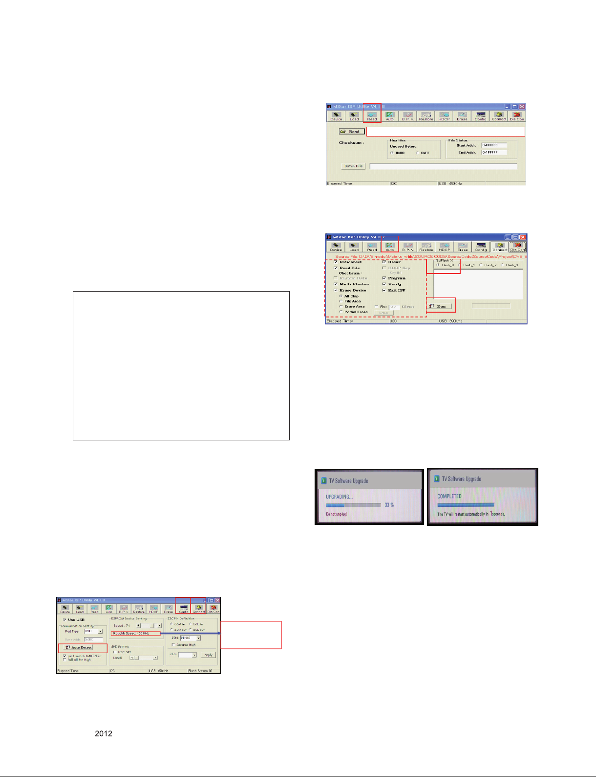
4) Click “Read” tab, and then load download file(XXXX.bin) by
clicking “Read”.
(4)
filexxx.bin
5) Click “Auto” tab and set as below.
6) Click “Run”.
7) After downloading, check “OK” message.
(5)
(5)
(7) ……….OK
* USB DOWNLOAD(*.epk file download)
1) Make New folder named “LG_DTV” and put ISP file(*.epk)
in the folder.
2) Put the USB Stick to the USB socket.
3) Automatically detecting update file in USB Stick
- If your downloaded program version in USB Stick is Low,
it didn’t work.
- Bu t your downloaded version is High, USB data is
automatically detecting
4) Show the message "Copying files from memory"
5) Updating is starting.
3. Main PCB check process
* APC - After Manual-Insult, executing APC
* Boot le Download
1) Execute ISP program “Mstar ISP Utility” and then click
“Config” tab.
2) Set as below, and then click “Auto Detect” and check “OK”
message. If display “Error”, Check connect computer, jig,
and set.
3) Click “Connect” tab. If display “Can’t”, Check connect
computer, jig, and set.
(1) (3)
Please Check the Speed :
Use the speed under
OK
Only for training and service purposes
200KHz.
6) Upd at in g Co mpleted, T he M ul ti-vision will re st ar t
automatically.
7) If your TV is turned on, check your updated version and
Tool option. (explain the Tool option, next stage)
* If downloading version is more high than your TV have,
TV can lost all channel data. In this case, you have to
channel recover. if all channel data is cleared, you didn’t
have a DTV/ATV test on production line.
* After downloading, have to adjust TOOL OPTION again.
1. Push "ADJ" key in service remote control.
2. Select "Tool Option 1" and push "OK" key.
3. Punch in the number. (Each model has their number.)
4. Completed selecting Tool option.
- 9 -
LGE Internal Use OnlyCopyright © LG Electronics. Inc. All rights reserved.
Page 10

3.1. EDID Process
3.1.1. EDID download
(1) Press "Power only" key of service remote control.
(2) Press the ADJ KEY on R/C and enter EZ ADJUST
(3) Enter EDID D/L mode by pushing "►" key at "11. EDID D/L".
(4) EDID download is executed automatically.
(5) Press EXIT key on service remote control.
<Caution>
- Never connect HDMI & D-sub Cable when download EDID.
- Download HDMI
* Edid data and Model option download (USB)
NO Item CMD 1 CMD 2 Data 0
Enter download
MODE
EDID data and
Model option
download
EZ ADJUST
0. Tool Option1
1. Tool Option2
2. Tool Option3
3. Tool Option4
4. Tool Option5
5. Tool Option6
6. Country Group
7. Area Option
8. ADC Calibration
9. White Balance
10. 10 Point WB
11. Test Pattern
12. EDID D/L ►
14. Touch Sensitivity Setting
15. Ext. Input Adjust
16. SPK Lipsync Adjust
17.SPDIF Lipsync Adjust
Download
‘Mode In’
Download A E 00 10 Automatically download
A A 0 0 When transfer the ‘Mode
EDID D/L
HDMI OK
RGB OK
Reset
Start
In’, Carry the command.
(The use of a internal Data)
3.2. Function Check
3.2.1. Check display and sound
*Check Input and Signal items. (cf. work instructions)
1) TV
2) AV (SCART/CVBS)
3) COMPONENT (480i)
4) RGB(PC : 1366 x 768 @ 60Hz)
5) HDMI(PC : 1366 x 768 @ 60Hz)
6) PC Audio In
* Display and Sound check is executed by Remote control
<Caution> Not to push the INSTOP key after completion if the
function inspection.
4. Total Assembly line process
4.1. Tool option & ADC Check
(1) Press "Power on" key of service remote control.
(2) Connect USB Port → USB to Serial Adapter (UC-232A) →
RS-232C cable → PC(RS-232C port)
(3) Write Model Name & Serial Number by use USB Port.
(4) Must check the serial number at the Customer Support
menu. (Refer to below.)
3.1.2. RGB EDID Data
(1) All models without 29MN33D(Product ID: 22984/HEXA: 59C8)
*(week), **(year), ***(Check sum) : Adjustable Data
: Screen size, : Color Characteristics
3.1.3. HDMI EDID Data
(1) All models(Product ID: 22986/HEXA:59CA)
*(week), **(year), ***(Check sum) : Adjustable Data
**** (physical address): (HDMI : 10), ****(Check sum): (HDMI : CE)
: Screen size, : Color Characteristics
4.2. Model name & Serial number download
4.2.1. Model name & Serial number D/L
1) Press "Power on" key of service remote control.
2) Connect RS232 Signal Cable to RS-232 Jack.
3) Write Model Name & Serial Number by use RS-232.
4) Must check the serial number at the Diagnostics of SET UP
menu. (Refer to below.)
4.2.2. Method & notice
(1) Model Name & Serial Number D/L is using of scan equipment.
(2) Setting of scan equipment operated by Manufacturing
Technology Group.
(3) Serial number D/L must be conformed when it is produced
in production line, because serial number D/L is mandatory
by D-book 4.0.
*Manual Download (Model Name and Serial Number)
If the TV set is downloaded By OTA or Service man,
Sometimes model name or serial number is initialized. (Not
always) There is impossible to download by bar code scan,
so It need Manual download.
1) Press the 'Instart' key of ADJ remote control.
2) Go to the menu '6.Model Number D/L' like below photo.
3) Input the Factory model name(ex 24LN4500) or Serial
number like photo.
4) Check the model name Instart menu → Factory name
displayed (ex 24LN4500)
5) Check the Diagnostics (DTV country only) → Buyer
model displayed (ex 24LN4500)
Only for training and service purposes
- 10 -
LGE Internal Use OnlyCopyright © LG Electronics. Inc. All rights reserved.
Page 11

4.3. Function Check
4.3.1. Check display and sound
■ Check Input and Signal items. (cf. work instructions)
1) TV
2) AV (SCART/CVBS)
3) COMPONENT (480i)
4) RGB(PC : 1366 x 768 @ 60Hz)
5) HDMI(PC : 1366 x 768 @ 60Hz)
6) PC Audio In
* Display and Sound check is executed by Remote control
* Caution : Not to push the INSTOP KEY after completion if
the function inspection.
4.3.2. PIP Check
(1) Press “Power on” key of service remote control.
(2) Input RGB & TV(ATV or DTV) signal.
(3) Set Input mode to RGB.
(4) Press ‘PIP” key of ADJ remote control
(5) Check TV Video & Audio signal of Sub picture.
4.3.3. HDMI MHL function Inspection(HDMI2 port only)
(1) Insert HDMI cable for MHL function JIG connected to
HDMI2 port of the SET.
(2) Check that LED of JIG is green light and check that set
screen is correctly worked.
(3) If NG situation or other HDMI jack connection, LED of JIG
is red light and screen is not displayed.
4.4. White balance adjustment
- Equipment
(1) Color Analyzer: CA-210 (LED Module : CH 14)
(2) Adj. Computer(During auto adj., RS-232C protocol is
needed)
(3) Adjust Remote control
RGB Gains are fixed data for each model.
Insert RS-232C Jack which is connected with PC for White
Balance or equivalent device.
→ Total Assembly line should be check whether the color
coordinate(x,y) data refer to below table were meet or not.
- Cool Panel
Cool 13,000 K
Color
Temperature
Medium 9,300 K
Warm 6,500 K
Luminance
(cd/m²)
Cool Min : 80 K Typ : 110
Medium Min : 80 K Typ : 110
Warm Min : 70 K Typ : 110
* Note : x,y coordinates are drifted about 0.007 after 30 mins
heat-run. So checking color coordinate within 5-min at
total assembly line, consider x,y coordinates might be
up to 0.007 than x,y target of each color temperature.
* Note : Manual W/B process using adjusts Remote control.
1) After enter Service Mode by pushing "ADJ" key,
2) Enter "White Balance" by pushing "►" key at "White
Balance".
EZ ADJUST
0. Tool Option1
1. Tool Option2
2. Tool Option3
3. Tool Option4
4. Tool Option5
5. Tool Option6
6. Country Group
7. Area Option
8. ADC Calibration
9. White Balance
10. 10 Point WB
11. Test Pattern
12 EDID D/L
13. Sub B/C
14. Touch Sensitivity Setting
15. Ext. Input Adjust
16. SPK Lipsync Adjust
17.SPDIF Lipsync Adjust
* When doing Adjustment, Please make circumstance as
below.
X=0.276 (±0.03)
Y=0.275 (±0.03)
X=0.290 (±0.03)
Y=0.298 (±0.03)
X=0.318 (±0.03)
Y=0.334 (±0.03)
Whit Balance
Color Temp. ◄ ►
R-Gain
G-Gain
B-Gain
R-Cut
G-Cut
B-Cut
Test-Pattern
Backlight
Reset To Set
<Test Signal>
Inner pattern
(204gray,80IRE)
<Test Signal>
Inner pattern
(204gray,80IRE)
Cool
100
104
192
64
64
64
ON
100
MHL Function JIG(OK) MHL Function JIG(NG)
Only for training and service purposes
- 11 -
LGE Internal Use OnlyCopyright © LG Electronics. Inc. All rights reserved.
Page 12

4.5. DPM Operation check
■ Measurement Condition: 100-240V@ 50/60Hz
(1) Set Input to RGB-PC and connect D-sub cable to set -
RGB Mode.
Set Input to HDMI(with Input Label set to PC) and connect
HDMI cable to set - HDMI Mode
(2) Cut off H sync or V sync of signal.
(3) Check DPM operation refer to the below table.
Operating Condition Sync(H/V) Video LED(SET) Wattage(W)
Power S/W On
■ HDMI DPM Operating condition
- Input Label: HDMI (PC&DVI Mode)
Sleep mode -
RGB, HDMI
DPM X O
Off/Off Off Amber 1
MHL Cable HDMI & HDMI to DVI Cable
4.6. Model name & SW version & Adjust check
* Press the ‘Instart’ key of ADJ remote control.
4.6.1. Model Name& SW Version Check
(1) Check ‘Model Name’.
(2) Check ‘S/W Version’ (Refer to the IC Ver. in the BOM)
4.6.2. Adjust Check
(1) Check ‘Country Group’
(2) Check ‘Area Option’
(3) Check ‘Tool Option’ (Refer to the BOM Comments)
(4) Check ‘Adjust ADC[Comp&RGB]’ is OK.
(5) Check ‘EDID[RGB&HDMI]’ is OK.
* After check all, Press the 'EXIT' key of ADJ remote control to
go out SVC menu.
4.7. Outgoing condition Configuration
* After all function test, press IN-STOP key by SVC Remote
control. And make Outgoing Condition.
Only for training and service purposes
- 12 -
LGE Internal Use OnlyCopyright © LG Electronics. Inc. All rights reserved.
Page 13

1. No Power
TROUBLE SHOOTING
Check C820 All
Voltage Level (19V)
Y
Check IC809 Output
Voltage Level (3.3V_ST)
Y
Check IC802 output
Voltage Level (12V)
Y
Check IC810 Output
Voltage Level (2.5V)
Y
Check IC807 Output
Voltage Level (1.5V)
Y
Check IC806 Output
Voltage Level (1.15V)
Y
Check X201 Clock
24MHz
N N
N
N
N
N
N
N
Check Power connector
OK ?
Replace IC809
Replace IC802 &
Recheck
Replace IC810
Replace IC807
Replace IC806
Replace X201
Replace Adapter
Y
Replace IC100 Flash Memory
Only for training and service purposes
- 13 -
LGE Internal Use OnlyCopyright © LG Electronics. Inc. All rights reserved.
Page 14

2. No Picture
Module
Back Light On ?
Y
Check Panel power
P601(#27,28,29,30) 12V
IC804Output 12V
Y
Check Panel clock
P601(#9,10)
Y
Check FFC Cable for damage
or open conductors.
Y
Replace T-con
Board or module
N N
Check WLED_ENABLE high
Check LED Driver output
(LED Driver B’d P1101
N
N
N
R131
Y
#1,2,3,4,9,10,11,12)
Replace IC804
Check IC101
Repair Main B/D
Replace Cable
Check IC101
Replace Main Scaler IC
N
Check LED Driver IC1100
Replace LED Driver IC
3. No Video - Digital TV
Check RF Cable
Y
1. Check Tuner(TU2603 #5) Power (3.3V)
2. Check IC803 Output voltage(3.3V)
Y
1. Check Tuner(TU2602 #7) Power (1.8V)
2. Check IC805 Output voltage(1.8V)
Y
Check T uner(TU2602) I2C Signal
SCL(R3735), SDA(R3736)
Y
Check T uner(TU2603)
Data, CLK, SYN, VAL
N
N
N
N
Replace IC803
Replace IC805
Check IC101
Replace Tuner(TU2603)
Recheck
Only for training and service purposes
- 14 -
LGE Internal Use OnlyCopyright © LG Electronics. Inc. All rights reserved.
Page 15

4. No Video - Component
Check input signal format
Is it supported?
Y
Check Component Cable
Y
Check JK2800
Y
Check signal
R239,R237,R241
C220,C218,C222
Y
IC101 has problem
5. No Video - RGB
Check input signal format
Is it supported?
Wave f orm of Comp Y
N
Replace JK2800 or
Wave f orm of Comp Pb
Wave f orm of Comp Pr
Check Device
N
Replace R239,R237,R241
C220,C218,C222
Wave f orm of C220
Wave f orm of C218
Wave f orm of C222
Y
Check RGB Cable
Y
Check JK400
Y
Check Hsync, Vsync
R4024, R4025
Y
Check signal RGB
R228,R230,R232
C204,C206,C208
Y
IC101 has problem
Only for training and service purposes
N
N
N
Replace JK400 or
Check Device
Replace R4024, R4025
Replace R228,R230,R232
C204,C206,C208
Wave f orm of R228/C204
- 15 -
Wave f orm of R4025(Vsync)
Wave f orm of R230/C206
Wave f orm of R4024(Hsync)
Wave f orm of R232/C208
LGE Internal Use OnlyCopyright © LG Electronics. Inc. All rights reserved.
Page 16

6. No Video - HDMI
Check input signal format
Is it supported?
Y
Check HDMI Cable for damage
or open connector
Y
Check JK500,501
for proper connection or damage
Y
N
Replace connector
Check I2C Signal (JK500,501)
(#15, #16)
Y
Check HDCP Key (IC101)
7. No Audio
Make sure you can’t hear any audio and
Device support the audio signal normally.
Y
Check Speaker and
its wire connection (P700)
and the resistance
Y
Check R4045 Voltage Level (3.3V)
N
N
N
N
Replace connector or Speaker
Re download EDID data
Replace Scaler(IC101)
Replace IC807(3.3V)
Y
Check Signal from IC700
L700,L701, L706, L709
Y
Check Signal from IC101
SDA/SCL
(R703/R214, R707/R213)
Only for training and service purposes
N
N
Replace IC700
Replace IC101
- 16 -
LGE Internal Use OnlyCopyright © LG Electronics. Inc. All rights reserved.
Page 17

BLOCK DIAGRAM
PCMC IA Sl ot
Option(Only for DVB)
Option
IC502
Buffer
CI_CL K
CI_VIAL Er ror
CI_SYNC
CI_DATA[0~7]
74LVC541A
FE_TS_CLK
FE_TS_VAL Error
FE_TS_SYNC
FE_TS_DATA
(DVB T/C)
LGI T HALF l NIM
CI_ADDR[0~ 14]
REG
CI_OE
CI_IORD
CI_IOWR
CI-WE
CI ADDR[0~7]
System
EEPROM
EEPROM SCL & SDA
PCM_ DATA [0~7]
F_RB
PF-OE
Flash
SERIAL
Panel
DDR3: 800MHz
1GB
NAND Fl ash
1 Ch
LVDS
(1GB)
DDR3 SDRAM
2GB
DDR3 SDRAM
PF_CE O
SPI_CK
SPI_CI
SPI_CS
SPI_D O
DDR2
Address[0:12]
DDR2 Data [0:15]
DDR2
Address[0:12]
DDR2 Data [0:15]
Buffer
IC501
74LCX244
[0~7]
PCM_ A
PCM_ A
Buffer_FE _TS_CLK
Buffer_FE _TS_VAL Error
FE_DE_ SDA&SCL
[0~14]
(MSD804KKX)
LGE2121-MS10
Mstar M1(L13)
SIF
Buffer_FE _TS_SYNC
Buffer_FE _TS_DATA[0]
- ATSC: TDSS-H501F (Half NIM)
- ISDB - T : TDSN- B601F (Full NIM)
- DVB- T/C : TDSS-G501D(Half NIM)
FE_Tun er_SDA&SCL
TV L&R Soun d
CVBS& Scart R GB
SCART_OUT
SCART (Fu ll)
Option(Only for DVB)
Audi o IN
COMPONENT
COMP_ L & R_IN
COMP_ Y , Pb ,P r
Headp hone
HDMI_TM DS & HDMI I 2C
MAX3232CDR
CVBS
DSUB_R /G/B/H/V
AP2191DSG
RGB
USB (Jpeg,MP 3,DVIX)
HDMI(MHL)
Option
Only for training and service purposes
AMP SCL&SDA
HP L & R o ut
Audi o_ Master_CLK
/DATA[3]
(NTP7513)
Digital amp
WLED_ENABL E
OVP_SEL
CH_SEL
WLED_D IM_ADJ
DMB
[LED Driver IC]
WLED-Status
SP (L)
SP (R)
- 17 -
RS-232C
[Option : Only h otel model]
LGE Internal Use OnlyCopyright © LG Electronics. Inc. All rights reserved.
Page 18

400
EXPLODED VIEW
IMPORTANT SAFETY NOTICE
Many electrical and mechanical parts in this chassis have special safety-related characteristics. These
parts are identified by in the Schematic Diagram and EXPLODED VIEW.
It is essenti al that these special safet y parts shoul d be replac ed with the same compo nents as
recommended in this manual to prevent X-RADIATION, Shock, Fire, or other Hazards.
Do not modify the original design without permission of manufacturer.
401
120
521
540
LV1
122
910
800
900
801
200
301
300
Only for training and service purposes
- 18 -
501
511
A2 A31
510
531
LGE Internal Use OnlyCopyright © LG Electronics. Inc. All rights reserved.
Page 19

/F_RB
Copyright © 2013 LG Electronics. Inc. All rights reserved.
Only for training and service purposes
LGE Internal Use Only
/PF_OE
/PF_CE0
/PF_CE1
PF_ALE
/PF_WE
/PF_WP
NC_1
NC_2
NC_3
NC_4
NC_5
NC_6
R/B
RE
CE
NC_7
NC_8
VCC_1
VSS_1
NC_9
NC_10
CLE
ALE
WE
WP
NC_11
NC_12
NC_13
NC_14
NC_15
DIMMING
BLU_CURRENT_CTL
NAND FLASH MEMORY
AR103
AR104
NON BR(NAND_1G_SS)
EAN61857001
IC102-*1
K9F1G08U0D-SCB0
1
2
3
4
5
6
7
8
9
10
11
12
13
14
15
16
17
18
19
20
21
22
23
24
WLED_DIM_ADJ
EEPROM
IC103
AT24C256C-SSHL-T
NVRAM_ATMEL
A0
1
A1
2
A0’h
A2
3
GND
4
EAN61133501
22
+3.3V_Normal
22
C100
1uF
OPT
8
7
6
5
R102
3.3K
NON BR(NAND_1G_HYNIX_9103(DEV))
IC102
NC_1
NC_2
NC_3
NC_4
NC_5
NC_6
R/B
NC_7
NC_8
NC_9
CLE
ALE
RE
CE
WE
WP
H27U1G8F2CTR-BC
1
EAN35669103
2
3
4
5
6
7
8
9
10
11
12
13
14
15
16
17
18
19
20
21
22
23
24
48
47
46
45
44
43
42
41
40
39
38
37
36
35
34
33
32
31
30
29
28
27
26
25
NC_29
NC_28
NC_27
NC_26
I/O7
I/O6
I/O5
I/O4
NC_25
NC_24
NC_23
VDD_2
VSS_2
NC_22
NC_21
NC_20
I/O3
I/O2
I/O1
I/O0
NC_19
NC_18
NC_17
NC_16
NC_29
48
NC_28
47
NC_27
46
NC_26
45
I/O7
44
I/O6
43
I/O5
42
I/O4
41
NC_25
40
NC_24
39
NC_23
38
VCC_2
37
VSS_2
36
NC_22
35
NC_21
34
NC_20
33
I/O3
32
I/O2
31
I/O1
30
I/O0
29
NC_19
28
NC_18
27
NC_17
26
NC_16
25
BR(NAND_2G_HYNIX(DEV))
NC_1
1
NC_2
2
NC_3
3
NC_4
4
NC_5
5
NC_6
6
R/B
7
RE
8
CE
9
NC_7
10
NC_8
11
VCC_1
12
VSS_1
13
NC_9
14
NC_10
15
CLE
16
ALE
17
WE
18
WP
19
NC_11
20
NC_12
21
NC_13
22
NC_14
23
NC_15
24
+3.3V_Normal
C102
10uF
10V
C103
0.1uF
EAN60708702
IC102-*3
H27U2G8F2CTR
22
AR101
AR102
48
47
46
45
44
43
42
41
40
39
38
37
36
35
34
33
32
31
30
29
28
27
26
25
PCM_A[7]
PCM_A[6]
PCM_A[5]
PCM_A[4]
PCM_A[3]
PCM_A[2]
PCM_A[1]
PCM_A[0]
22
NC_29
NC_28
NC_27
NC_26
I/O7
I/O6
I/O5
I/O4
NC_25
NC_24
NC_23
VCC_2
VSS_2
NC_22
NC_21
NC_20
I/O3
I/O2
I/O1
I/O0
NC_19
NC_18
NC_17
NC_16
PCM_A[0-7]
BR(NAND_2G_TOSHIBA(DEV))
NC_1
1
NC_2
2
NC_3
3
NC_4
4
NC_5
5
NC_6
6
RY/BY
7
RE
8
CE
9
NC_7
10
NC_8
11
VCC_1
12
VSS_1
13
NC_9
14
NC_10
15
CLE
16
ALE
17
WE
18
WP
19
NC_11
20
NC_12
21
NC_13
22
NC_14
23
NC_15
24
EAN60991001
TC58NVG1S3ETA00
+3.3V_Normal
R109
3.9K
1K
OPT
C101
1K
0.1uF
VCC_1
VSS_1
NC_10
NC_11
NC_12
OPT
R105
1K
R106
1K
R107
R108
NC_13
NC_14
NC_15
NON BR(NAND_1G_NUMONYX(DEV))
EAN60762401
IC102-*2
NAND01GW3B2CN6E
NC_29
48
NC_28
47
NC_27
46
NC_26
45
I/O7
44
I/O6
43
I/O5
42
I/O4
41
NC_25
40
NC_24
39
NC_23
38
VCC_2
37
VSS_2
36
NC_22
35
NC_21
34
NC_20
33
I/O3
32
I/O2
31
I/O1
30
I/O0
29
NC_19
28
NC_18
27
NC_17
26
NC_16
25
NC_1
NC_2
NC_3
NC_4
NC_5
NC_6
NC_7
NC_8
VDD_1
VSS_1
NC_9
NC_10
NC_11
NC_12
NC_13
NC_14
NC_15
1
2
3
4
5
6
RB
7
R
8
E
9
10
11
12
13
14
15
CL
16
AL
17
W
18
WP
19
20
21
22
23
24
<CHIP Config(LED_R/BUZZ)>
Boot from SPI CS1N(EXT_FLASH) 1’b0
Boot from SPI_CS0N(INT_FLASH) 1’b1
<CHIP Config>
(I2S_OUT_BCK,I2S_OUT_MCK,PAD_PWM1PAD_PWM0)
B51_no_EJ : 4’b0000 Boot from 8051 with SPI flash
SB51_WOS : 4’b0001 Secure B51 without scramble
SB51_WS : 4’b0010 Secure B51 with scramble
MIPS_SPE_NO_EJ : 4’b0100 Boot from MIPS with SPI flash
MIPS_SPI_EJ_1 : 4’b0101 Boot from MIPS with SPI flash
MIPS_SPI_EJ_2 : 4’b0110 Boot from MIPS with SPI flash
MIPS_WOS : 4’b1001 Secure MIPS without scramble
MIPS_WS : 4’b1010 Scerur MIPS with SCRAMBLE
4.7K
+3.3V_Normal
4.7K
OPT
R117
R115
AUD_MASTER_CLK
IC102-*4
48
47
46
45
44
43
42
41
40
39
38
37
36
35
34
33
32
31
30
29
28
27
26
25
NC_29
NC_28
NC_27
NC_26
I/O8
I/O7
I/O6
I/O5
NC_25
NC_24
NC_23
VCC_2
VSS_2
NC_22
NC_21
NC_20
I/O4
I/O3
I/O2
I/O1
NC_19
NC_18
NC_17
NC_16
OPT
C112
100pF
50V
R148
33
4.7K
4.7K
R116
R118
LGE2121-NonMS10 (MSD804KKX)
: EAN62651201 (KR/US REGION)
LGE2121-MS10 (MSD804KKX)
: EAN62674101 (NON_KR/US REGION)
OPT
4.7K
R165
4.7K
R121
OPT
W21
AA18
AB22
AE20
AA15
AE21
AB21
Y15
W20
V20
W22
AB18
AA20
AA21
Y19
AB17
Y16
AB19
AB20
AA16
AA19
AC21
AA17
Y20
AB15
AA22
AD22
AD20
AD21
AC20
Y18
Y21
Y22
U21
V21
R20
T20
U22
D4
E4
N25
N24
B8
A8
P23
P24
D2
D1
P21
N23
P22
R21
P20
F6
H6
G5
G4
J5
J4
R23
R24
R25
T21
T22
+3.3V_ST
4.7K
4.7K
OPT
OPT
R123
R142
4.7K
4.7K
R143
R124
S7LR-M_MS10(NON KR/US)
IC101-*1
LGE2121-MS (M1_L13_MS10)
PCMDATA[0]/GPIO129
PCMDATA[1]/GPIO130
PCMDATA[2]/GPIO131
PCMDATA[3]/GPIO123
PCMDATA[4]/GPIO122
PCMDATA[5]/GPIO121
PCMDATA[6]/GPIO120
PCMDATA[7]/GPIO119
PCMADR[0]/GPIO128
PCMADR[1]/GPIO127
PCMADR[2]/GPIO125
PCMADR[3]/GPIO124
PCMADR[4]/GPIO102
PCMADR[5]/GPIO104
PCMADR[6]/GPIO105
PCMADR[7]/GPIO106
PCMADR[8]/GPIO111
PCMADR[9]/GPIO113
PCMADR[10]/GPIO117
PM_UART_TX/GPIO_PM[1]/GPIO7
PCMADR[11]/GPIO115
PCMADR[12]/GPIO107
PCMADR[13]/GPIO110
PCMADR[14]/GPIO109
PM_UART_RX/GPIO_PM[5]/GPIO11
PM_SPI_SCZ1/GPIO_PM[6]/GPIO12
PCMREG_N/GPIO126
PCMOE_N/GPIO116
PCMWE_N/GPIO195
PM_SPI_SCZ2/GPIO_PM[10]/GPIO16
PCMIORD_N/GPIO114
PCMIOWR_N/GPIO112
PCMCE_N/GPIO118
PM_SPI_CZ0/GPIO_PM[12]/GPIO0
PCMIRQA_N/GPIO108
PCMCD_N/GPIO133
PCMWAIT_N/GPIO103
PCM_RESET/GPIO132
PCM2_CE_N/GPIO134
PCM2_IRQA_N/GPIO135
PCM2_CD_N/GPIO138
PCM2_WAIT_N/GPIO136
PCM2_RESET/GPIO137
UART1_TX/GPIO46
UART1_RX/GPIO47
UART2_TX/GPIO68
UART2_RX/GPIO67
UART3_TX/GPIO50
UART3_RX/GPIO51
I2C_SCKM2/DDCR_CK/GPIO75
I2C_SDAM2/DDCR_DA/GPIO74
DDCA_DA/UART0_TX
DDCA_CK/UART0_RX
PWM0/GPIO69
PWM1/GPIO70
PWM2/GPIO71
PWM3/GPIO72
PWM4/GPIO73
PWM_PM/GPIO197
SAR0/GPIO34
SAR1/GPIO35
SAR2/GPIO36
SAR3/GPIO37
SAR4/GPIO38
VSYNC_LIKE/GPIO146
SPI1_CK/GPIO199
SPI1_DI/GPIO200
SPI2_CK/GPIO201
SPI2_DI/GPIO202
OPT
OPT
4.7K
R153
GPIO_PM[11]/GPIO17
TS0DATA_[0]/GPIO80
TS0DATA_[1]/GPIO81
TS0DATA_[2]/GPIO82
TS0DATA_[3]/GPIO83
TS0DATA_[4]/GPIO84
TS0DATA_[5]/GPIO85
TS0DATA_[6]/GPIO86
TS0DATA_[7]/GPIO87
TS1DATA_[0]/GPIO91
TS1DATA_[1]/GPIO92
TS1DATA_[2]/GPIO93
TS1DATA_[3]/GPIO94
TS1DATA_[4]/GPIO95
TS1DATA_[5]/GPIO96
TS1DATA_[6]/GPIO97
TS1DATA_[7]/GPIO98
R152
4.7K
R103 0
R100 0
OPT
NF_CE1Z/GPIO141
NF_WPZ/GPIO196
NF_CEZ/GPIO140
NF_CLE/GPIO139
NF_REZ/GPIO142
NF_WEZ/GPIO143
NF_ALE/GPIO144
NF_RBZ/GPIO145
GPIO_PM[0]/GPIO6
GPIO_PM[2]/GPIO8
GPIO_PM[3]/GPIO9
GPIO_PM[4]/GPIO10
GPIO_PM[7]/GPIO13
GPIO_PM[8]/GPIO14
GPIO_PM[9]/GPIO15
PM_SPI_SCK/GPIO1
PM_SPI_SDI/GPIO2
PM_SPI_SDO/GPIO3
TS0CLK/GPIO90
TS0VALID/GPIO88
TS0SYNC/GPIO89
TS1CLK/GPIO101
TS1VALID/GPI99
TS1SYNC/GPIO100
AE18
AC17
AD18
AC18
AC19
AD17
AE17
AD19
H5
K6
K5
J6
K4
L6
C2
L5
M6
M5
C1
M4
A2
D3
B2
B1
Y14
AA10
Y12
Y13
Y11
AA12
AB12
AA14
AB14
AA13
AB11
AC15
AD15
AC16
AD16
AE15
AE14
AC13
AC14
AD12
AD13
AD14
LED_AMBER
LED_RED
SPI_SDI
AUD_SCK
AUD_MASTER_CLK_0
PWM1
PWM0
for SYSTEM EEPROM
(IC104)
120915
PCM_5V_CTL Deleted
120917
Changed
I2C_SCL
I2C_SDA
RGB_DDC_SDA
RGB_DDC_SCL
2012.09.15
SCART1_MUTE Delete
120915
PCM_DATA Deleted
PCM_A[0-7]
USB_OCD
USB_CTL
/MHL_OCP_DET
MHL_OCP_EN
PM_TXD
PM_RXD
MODEL_OPT_6
MODEL_OPT_7
ERROR_OUT
LED_AMBER
KEY1
KEY2
2011.11.15
WalkieTalkie Issue
KEY_SCL
KEY_SDA
LED_RED
PCM_A[0]
PCM_A[1]
PCM_A[2]
PCM_A[3]
PCM_A[4]
PCM_A[5]
PCM_A[6]
PCM_A[7]
120915
PCM_DATA Deleted
PWM0
PWM1
PWM2
C107
0.1uF
16V
R101 22
R163 22
R164 22
R136 22
R137 22
R154 22
R113 22
C110
0.1uF
16V
S7LR-M_NON_MS10(KR/US)
W21
PCMDATA[0]/GPIO129
AA18
PCMDATA[1]/GPIO130
AB22
PCMDATA[2]/GPIO131
AE20
PCMDATA[3]/GPIO123
AA15
PCMDATA[4]/GPIO122
AE21
PCMDATA[5]/GPIO121
AB21
PCMDATA[6]/GPIO120
Y15
PCMDATA[7]/GPIO119
W20
PCMADR[0]/GPIO128
V20
PCMADR[1]/GPIO127
W22
PCMADR[2]/GPIO125
AB18
PCMADR[3]/GPIO124
AA20
PCMADR[4]/GPIO102
AA21
PCMADR[5]/GPIO104
Y19
PCMADR[6]/GPIO105
AB17
PCMADR[7]/GPIO106
Y16
PCMADR[8]/GPIO111
AB19
PCMADR[9]/GPIO113
AB20
PCMADR[10]/GPIO117
AA16
PCMADR[11]/GPIO115
AA19
PCMADR[12]/GPIO107
AC21
PCMADR[13]/GPIO110
AA17
PCMADR[14]/GPIO109
Y20
PCMREG_N/GPIO126
AB15
PCMOE_N/GPIO116
AA22
PCMWE_N/GPIO195
AD22
PCMIORD_N/GPIO114
AD20
PCMIOWR_N/GPIO112
AD21
PCMCE_N/GPIO118
AC20
PCMIRQA_N/GPIO108
Y18
PCMCD_N/GPIO133
Y21
PCMWAIT_N/GPIO103
Y22
PCM_RESET/GPIO132
U21
PCM2_CE_N/GPIO134
V21
PCM2_IRQA_N/GPIO135
R20
PCM2_CD_N/GPIO138
T20
PCM2_WAIT_N/GPIO136
U22
PCM2_RESET/GPIO137
D4
UART1_TX/GPIO46
E4
UART1_RX/GPIO47
N25
UART2_TX/GPIO68
N24
UART2_RX/GPIO67
B8
UART3_TX/GPIO50
A8
UART3_RX/GPIO51
P23
I2C_SCKM2/DDCR_CK/GPIO75
P24
I2C_SDAM2/DDCR_DA/GPIO74
D2
DDCA_DA/UART0_TX
D1
DDCA_CK/UART0_RX
P21
PWM0/GPIO69
N23
PWM1/GPIO70
P22
PWM2/GPIO71
R21
PWM3/GPIO72
P20
PWM4/GPIO73
F6
PWM_PM/GPIO197
H6
SAR0/GPIO34
G5
SAR1/GPIO35
G4
SAR2/GPIO36
J5
SAR3/GPIO37
J4
SAR4/GPIO38
R23
VSYNC_LIKE/GPIO146
R24
SPI1_CK/GPIO199
R25
SPI1_DI/GPIO200
T21
SPI2_CK/GPIO201
T22
SPI2_DI/GPIO202
IC101
MSD804KKX
NF_CE1Z/GPIO141
NF_WPZ/GPIO196
NF_CEZ/GPIO140
NF_CLE/GPIO139
NF_REZ/GPIO142
NF_WEZ/GPIO143
NF_ALE/GPIO144
NF_RBZ/GPIO145
GPIO_PM[0]/GPIO6
PM_UART_TX/GPIO_PM[1]/GPIO7
GPIO_PM[2]/GPIO8
GPIO_PM[3]/GPIO9
GPIO_PM[4]/GPIO10
PM_UART_RX/GPIO_PM[5]/GPIO11
PM_SPI_SCZ1/GPIO_PM[6]/GPIO12
GPIO_PM[7]/GPIO13
GPIO_PM[8]/GPIO14
PM_SPI_SCZ2/GPIO_PM[10]/GPIO16
GPIO_PM[9]/GPIO15
GPIO_PM[11]/GPIO17
PM_SPI_SCK/GPIO1
PM_SPI_CZ0/GPIO_PM[12]/GPIO0
PM_SPI_SDI/GPIO2
PM_SPI_SDO/GPIO3
TS0CLK/GPIO90
TS0VALID/GPIO88
TS0SYNC/GPIO89
TS0DATA_[0]/GPIO80
TS0DATA_[1]/GPIO81
TS0DATA_[2]/GPIO82
TS0DATA_[3]/GPIO83
TS0DATA_[4]/GPIO84
TS0DATA_[5]/GPIO85
TS0DATA_[6]/GPIO86
TS0DATA_[7]/GPIO87
TS1CLK/GPIO101
TS1VALID/GPI99
TS1SYNC/GPIO100
TS1DATA_[0]/GPIO91
TS1DATA_[1]/GPIO92
TS1DATA_[2]/GPIO93
TS1DATA_[3]/GPIO94
TS1DATA_[4]/GPIO95
TS1DATA_[5]/GPIO96
TS1DATA_[6]/GPIO97
TS1DATA_[7]/GPIO98
AE18
AC17
AD18
AC18
AC19
AD17
AE17
AD19
H5
K6
K5
J6
K4
L6
C2
L5
M6
M5
C1
M4
A2
R147 33
D3
B2
B1
for SERIAL FLASH
Y14
AA10
Y12
Y13
Y11
AA12
AB12
AA14
AB14
AA13
AB11
AC15
AD15
AC16
AD16
AE15
AE14
AC13
AC14
AD12
AD13
AD14
R146 33
R151 33
+3.3V_ST
R125
10K
120915
CI_TS_DATA Deleted
/PF_WP
/PF_CE0
/PF_CE1
/PF_OE
/PF_WE
PF_ALE
/F_RB
DSUB_DET
PM_TXD
5V_DET_HDMI_2
PM_RXD
/FLASH_WP
HP_MUTE
PANEL_CTL
5V_DET_HDMI_1
NTP_MUTE
SPI_SCK
/SPI_CS
SPI_SDI
OPT
R128
+3.3V_ST
R180
FE_TS_CLK
FE_TS_VAL_ERR
FE_TS_SYNC
FE_TS_DATA[0]
4.7K
Internal demod out
120915
FE_TS_DATA[1]~[7]
Deleted
50V
47K
C113
0.1uF
120915
Pull up added
SPI_SDO
MULTI_ON
POWER_ON/OFF1
+5V_Normal
PM MODEL OPTION
R178 100 OPT
R179 100 OPT
SERIAL FLASH MEMORY
/FLASH_WP
C111
2.2uF
R156
R157
I2C
10K
PWM0
100
PWM2
R140
1K
R141
1K
R160
4.7K
+3.3V_Normal
R161
4.7K
R144
2.2K
R145
2.2K
AMP_SDA
AMP_SCL
I2C_SDA
I2C_SCL
KEY_SDA
KEY_SCL
+3.3V_Normal
NVRAM_ST
IC103-*1
C105
0.1uF
VCC
WP
SCL
SDA
C104
8pF
OPT
R111 22
R112 22
C106
8pF
OPT
I2C_SCL
I2C_SDA
M24256-BRMN6TP
E0
1
E1
2
E2
3
VSS
4
EAN61548301
8
7
6
5
VCC
WC
SCL
SDA
NVRAM_RENESAS
IC103-*2
R1EX24256BSAS0A
A0
1
A1
2
A2
3
VSS
4
EAN62389501
VCC
8
WP
7
SCL
6
SDA
5
OPT
R174
10K
OPT
R175
10K
OPT
R135
10K
+3.3V_ST
+3.3V_ST
/SPI_CS
SPI_SDO
OPT
R177
10K
OPT
R176
10K
121018
Net Name Change
BOOT_POWER_OPTION_0
BOOT_POWER_OPTION_1
+3.3V_ST
S_FLASH_MAIN_WINBOND
OPT
R138
4.7K
CS
DO[IO1]
%WP[IO2]
GND
IC100
W25Q80BVSSIG
1
2
3
4
8
7
6
5
VCC
HOLD[IO3]
CLK
DI[IO0]
+3.3V_ST
R139
33
WLED_ENABLE
C114
0.1uF
SPI_SCK
SPI_SDI
R131
100
Q100
MMBT3904(NXP)
S_FLASH_MAIN_MACRONIX
MX25L8006EM2I-12G
CS#
SO/SIO1
WP#
GND
10K
C
E
4.7K
1
2
3
4
R130
R127
4.7K
B
121018
ADDED
120915
R129
SCART1_DET Delete
OPT
121018
ADDED
IC100-*1
R126
10K
AMP_RST
PC_AUDIO_DET
AV_CVBS_DET
MODEL_OPT_8
HP_DET
MODEL_OPT_9
TUNER_RESET
MODEL_OPT_0
MODEL_OPT_1
LNA_CTRL_1
LNA_CTRL_2
MODEL_OPT_2
BR_RESET_DEMOD
VCC
8
HOLD#
7
SCLK
6
SI/SIO0
5
applied on only SMALL PCB
OLP
S7LR-M_NON_MS10(KR/US)
C7
E6
F5
B6
E5
D5
B7
E7
F7
AB5
AB3
A9
F4
AB1
N6
AB2
AC2
IC101
MSD804KKX
GPIO39
GPIO40
GPIO41
GPIO42
GPIO43
GPIO44
GPIO45
GPIO48
GPIO49
GPIO52
GPIO53
GPIO54
GPIO55
I2C_SCKM0/GPIO56
I2C_SDAM0/GPIO57
GPIO76
GPIO77
LVA0P
LVA0N
LVA1P
LVA1N
LVA2P
LVA2N
LVA3P
LVA3N
LVA4P
LVA4N
LVB0P
LVB0N
LVB1P
LVB1N
LVB2P
LVB2N
LVB3P
LVB3N
LVB4P
LVB4N
LVACLKP
LVACLKN
LVBCLKP
LVBCLKN
GPIO194
GPIO191
GPIO192
GPIO193
AB25
AB23
AC25
AB24
AD25
AC24
AE23
AC23
AC22
AD23
V23
U24
V25
V24
W25
W23
AA23
Y24
AA25
AA24
AE24
AD24
Y23
W24
T25
U23
T24
T23
121019
ADDED to improve EMI
R182 22
R183 22
R184 22
R185 22
R186 22
R187 22
R188 22
R189 22
R158 22
R159 22
MODEL_OPT_3
MODEL_OPT_4
MODEL_OPT_5
RXA0+
RXA0RXA1+
RXA1RXA2+
RXA2RXA3+
RXA3-
RXACK+
RXACK-
THE SYMBOL MARK OF THIS SCHEMETIC DIAGRAM INCORPORATES
SPECIAL FEATURES IMPORTANT FOR PROTECTION FROM X-RADIATION.
FILRE AND ELECTRICAL SHOCK HAZARDS, WHEN SERVICING IF IS
ESSENTIAL THAT ONLY MANUFATURES SPECFIED PARTS BE USED FOR
THE CRITICAL COMPONENTS IN THE SYMBOL MARK OF THE SCHEMETIC.
NC4_S7LRM
MAIN1_NON_EU
EAX65077302
2012.11.18
1 12
Page 20

MODEL OPTION
Copyright © 2013 LG Electronics. Inc. All rights reserved.
Only for training and service purposes
LGE Internal Use Only
120915
Deleted
RF_SWITCH_CTL
MODEL OPTION
+3.3V_ST
+3.3V_Normal
OPT
OPT
(OPT)TAIWAN
R301 10K
R300 10K
R290 1K
100
BR(RF_SW_OPT)
R203
10K
10K
1K
ASIA
R302
R303
R293
BOOT_POWER_OPTION_0
121018
PM_MODEL_OPT_0
->BOOT_POWER_OPTION_0
121018
PM_MODEL_OPT_1
->BOOT_POWER_OPTION_1
BOOT_POWER_OPTION_1
CK+_HDMI2
HDMI
CK-_HDMI2
D0+_HDMI2
D0-_HDMI2
D1+_HDMI2
D1-_HDMI2
D2+_HDMI2
D2-_HDMI2
DDC_SDA_2
DDC_SCL_2
HPD2
CK+_HDMI1
CK-_HDMI1
D0+_HDMI1
D0-_HDMI1
D1+_HDMI1
D1-_HDMI1
D2+_HDMI1
D2-_HDMI1
DDC_SDA_1
DDC_SCL_1
HPD1
CEC_REMOTE_S7
DSUB_HSYNC
DSUB_VSYNC
DSUB_R+
DSUB_G+
DSUB
DSUB_B+
COMP
COMP_Pr+
COMP_Y+/AV_CVBS_IN
COMP_Pb+
CVBS In/OUT
TU_CVBS
COMP_Y+/AV_CVBS_IN
120918
DTV/MNT_VOUT deleted
R291 1K
R294 1K
R260
OPT
10K
+2.5V_Normal
OPT
OPT
R222 1K
R224 1K
R206 1K
MODEL_OPT_MIU0-256M(BR/ASIA)
R207 1K
R223 1K
R225 1K
MODEL_OPT_MIU0-128M(KR/US)
120715
Added
120715
Added
R266 510
R267 510
R228 33
R229 68
R230 33
R231 68
R232 33
R233 68
2.4K
R261
R237 33
R238 68
R239
R240
R241 33
R242 68
R244 33
R246 33
C203
50V
OPT
Close to MSTAR
R252 68
1000pF
+3.3V_Normal
OPT
ASIA
R208 1K
R211 1K
NON_ASIA
R212 1K
R209 1K
R218 22
R219 22
R220 22
R221 22
33
68
R226 1K
OPT
R227 1K
C204 0.047uF
C205 0.047uF
C206 0.047uF
C207 0.047uF
C208 0.047uF
C209 0.047uF
C210 1000pF
C218 0.047uF
C219 0.047uF
C220 0.047uF
C221 0.047uF
C222 0.047uF
C223 0.047uF
C224 1000pF
C225 0.047uF
C227 0.047uF
C233 0.047uF
MODEL_OPT_0
MODEL_OPT_1
MODEL_OPT_2
MODEL_OPT_3
MODEL_OPT_4
MODEL_OPT_0
MODEL_OPT_1
MODEL_OPT_2
MODEL_OPT_3
MODEL_OPT_4
MODEL_OPT_5
MODEL_OPT_6
MODEL_OPT_7
MODEL_OPT_8
MODEL_OPT_9
J2
J3
K3
J1
K2
K1
L2
L3
T5
T4
V5
R5
AE9
AC9
AC10
AD9
AC11
AD10
AE11
AD11
AE8
AD8
AC8
F2
F3
G3
F1
G2
G1
H2
H3
R6
U6
P5
R4
P2
R3
N2
P3
N3
N1
M3
M2
M1
V2
V3
U3
U2
T1
T2
R2
R1
T3
AA2
Y2
AA3
W2
Y3
V1
W3
W1
AA8
Y4
W4
AA5
Y5
AA4
Y6
AA1
AB4
MODEL_OPT_5
MODEL_OPT_7
MODEL_OPT_8
MODEL_OPT_9
S7LR-M_NON_MS10(KR/US)
RXACKP
RXACKN
RXA0P
RXA0N
RXA1P
RXA1N
RXA2P
RXA2N
DDCDA_DA/GPIO27
DDCDA_CK/GPIO26
HOTPLUGA/GPIO22
HOTPLUGD/GPIO25
RXCCKP
RXCCKN
RXC0P
RXC0N
RXC1P
RXC1N
RXC2P
RXC2N
DDCDC_DA/GPIO31
DDCDC_CK/GPIO30
HOTPLUGC/GPIO24
RXBCKP
RXBCKN
RXB0P
RXB0N
RXB1P
RXB1N
RXB2P
RXB2N
DDCDB_DA/GPIO29
DDCDB_CK/GPIO28
HOTPLUGB/GPIO23
CEC/GPIO5
HSYNC0
VSYNC0
RIN0P
RIN0M
GIN0P
GIN0M
BIN0P
BIN0M
SOGIN0
HSYNC1
VSYNC1
RIN1P
RIN1M
GIN1P
GIN1M
BIN1P
BIN1M
SOGIN1
HSYNC2
RIN2P
RIN2M
GIN2P
GIN2M
BIN2P
BIN2M
SOGIN2
CVBS0
CVBS1
CVBS2
CVBS3
NC_5
NC_7
NC_6
CVBSOUT1
VCOM
PIN NAME
MSD804KKX
IC101
PIN NO.
AB3
F4
AB2
T25
U23
T24
B8
A8
F7
A9
I2C_SCKM1/GPIO78
I2C_SDAM1/GPIO79
SPDIF_IN/GPIO150
SPDIF_OUT/GPIO151
I2S_IN_BCK/GPIO148
I2S_IN_SD/GPIO149
I2S_IN_WS/GPIO147
I2S_OUT_BCK/GPIO154
I2S_OUT_MCK/GPIO152
I2S_OUT_SD/GPIO155
I2S_OUT_WS/GPIO153
GPIO_PM[13]/GPIO19
GPIO_PM[14]/GPIO20
GPIO_PM[15]/GPIO21
LOW
FHD
NON_AJ
NON_DVB_T2
NON_M120
MIU0-128M
NON_DVB_S
MIU1-NO_DDR
Dual Stream is only Korea 3D spec
NON_DualStream
HD_LVDS_EU
EU,AJ
AC4
NC_8
AD3
NC_9
AC3
IP
AE3
IM
AD4
SIFP
AC5
SIFM
AD2
IF_AGC
AE2
RF_AGC
AE6
AD6
AD1
XIN
AC1
XOUT
D7
D6
E3
USB0_DM
E2
USB0_DP
AC12
USB1_DM
AE12
USB1_DP
C8
D8
D9
B10
C9
B9
C10
AB9
AUL0
AA11
AUR0
Y9
AUL1
AA9
AUR1
AA7
AUL2
AB8
AUR2
Y8
AUL3
Y10
AUR3
AC7
AUL4
AD7
AUR4
W6
V6
AUOUTL2
V4
AVDD5V_MHL
Y7
W5
AUOUTR2
U5
AD5
AUVRM
AE5
AUVAG
AC6
AUVRP
RP/GPIO63
TP/GPIO60
RN/GPIO66
TN/GPIO62
GPIO61
GPIO64
GPIO65
IRIN/GPIO4
ARC0
HWRESET
AA6
AB6
C6
C5
A6
C4
B5
C3
A3
B3
B4
N4
T6
N5
R210 0
EARPHONE_OUTL
EARPHONE_OUTR
LED1/GPIO59
LED0/GPIO58
AJ
MIU0-256M
DVB_S
MIU1-128MMODEL_OPT_6
DualStream
TUNER_I2C
1M
R287
R297 0OPT
R296 100OPT
R213 22
R214 22
120915
Deleted
C242
2.2uF
C243 2.2uF
C244 2.2uF
C245 2.2uF
MHL_CD_SENSE
AVDD5V_MHL
/VBUS_EN
TP209
C249
4.7uF
L203 LN45005.6uH
L205 LN45005.6uH
R264
49.9
LAN JACK
OPT
HIGH
HD
DVB_T2
M120
HD_LVDS_NON_EU
TAIWAN
Other: N.C
Close to MSTAR
R288 100
HALF_NIM
R289 100
HALF_NIM
C250 0.1uF
C251 0.1uF
ANALOG SIF
Close to MSTAR
+3.3V_Normal
R274
HALF_NIM
0
C282
0.1uF
HALF_NIM
TU_SCL
TU_SDA
C261 27pF
X201
24MHz
C262 27pF
120915
Deleted
120915
Deleted
C256
C253
0.1uF
1uF
R265
R262
49.9
49.9
LAN JACK
LAN JACK
C294
0.1uF
LAN JACK
C231 1uF
OPT
C257 0.1uF
HALF_NIM
C258 0.1uF
HALF_NIM
R234 47
R235 47
HALF_NIM
R243
10K
12.08.03
22->27pF
120715
Added
AMP_SCL
AMP_SDA
COMP_DET
BLM18SG121TN1D
C263
10uF
R263
49.9
LAN JACK
C295
0.1uF
LAN JACK
IR
HDMI_ARC
SOC_RESET
MEMORY OPTION
Model
OPT 4
OPT
ASIA(HALF_NIM/IF_FILTER)
C287
C288
100pF
33pF
C285
0.047uF
25V
HALF_NIM
SIDE USB
USB_DM
USB_DP
COMP_L_IN
COMP_R_IN
PC_L_IN
PC_R_IN
AUDIO IN
AUDIO OUT
12015
SCART1_LOUT,ROUT
Deleted
R275
0
LN4500
C268
4.7uF
10V
LN4500
0
1
ASIA(HALF_NIM/IF_FILTER)
C289
33pF
TU_SIF
R277
0
OPT
128M+128M
256M+128M
HALF_NIM
R247
0
L202
EPHY_RP
EPHY_TP
EPHY_RN
EPHY_TN
Memory
C264
1000pF
50V
256M
OPT
Close to MSTAR
Model
OPT 6
00128M
1
01
DTV_IF
IF_P_MSTAR
IF_N_MSTAR
120915
100->33pF
121118
APPLY
IF_AGC_MAIN
R276
0
LN4500
C272
4.7uF
10V
LN4500
R278
0
OPT
Ginga1
Note
H/P OUT
AUD_SCK
AUD_MASTER_CLK_0
AUD_LRCH
I2S_I/F
AUD_LRCK
HP_LOUT
HP_ROUT
SOC_RESET
C200
4.7uF
D200
MMBD6100
SB_MUTE
+1.15V_VDDC
ZD201
5.6B
(OPT)ZENER MainIC
111128
Zener Add
+3.3V_Normal
ZD202
5.6B
(OPT)ZENER MainIC
111128
Zener Add
+3.3V_ST
10V
A2CA1
10uFC228
0.1uF
C246 0.1uF
C239
STby 3.3V
111128
Zener Add
+1.5V_DDR
+1.15V_VDDC
R205
R200
62K
OPT
10uFC275
10uFC276
R268
0
1/10W
5%
R269
0
1/10W
5%
+3.3V_ST
5.6B
(OPT)ZENER MainIC
C306
0.1uF
R271
0
1/10W
5%
111026Switch
EBF32593901 Deletion
10
OPT
C201
0.1uF
C277 1uF
VDD33
10uFC284
AVDD_AU33
AVDD_NODIE:7.362mA
ZD203
OPT
C283 0.1uF
C280 1uF
C292 0.1uF
Normal Power 3.3V
OPT
OPT
10uFC254
10uFC293
C255 0.1uF
C240
0.1uF
AVDD_NODIE
R216
0
1/10W
5%
AVDD_MPLL
R217
0
1/10W
5%
AVDD_DVI
R215
0
1/10W
10uFC202
5%
C229 0.1uF
DDR3 1.5V
R270
0
1/10W
5%
C247
10uF
OPT
ZD200
3.3V
MIUVDDC
SOC_RESET
C248
0.1uF
C278
C299 0.1uF
C241
0.1uF
C286
0.1uF
C234
0.1uF
C235 0.1uF
10uF
OPT
C259 0.1uF
C281
C260 0.1uF
OPT
C266 0.1uF
10uF OPT
VDDC 1.15V
OPT
OPT
OPT
C298 0.1uF
C291 0.1uF
OPT
C297 0.1uF
C279 0.1uF
C301 0.1uF
C252
0.1uF
AVDD_DDR0:55mA
AVDD_DDR1:55mA
C290
AVDD_MIU
OPT
C296
C300
0.1uF
0.1uF OPT
Normal 2.5V
+2.5V_Normal
ZD204
5.6B
111128
Zener Add
(OPT)ZENER MainIC
OPT
C302 0.1uF
OPT
C265 0.1uF
0.1uF
R273
0
1/10W
5%
C303
R272
0
1/10W
5%
OPT
C304 0.1uF
OPT
C267 0.1uF
0.1uF
OPT
C232 0.1uF
C305
1uF
AVDD2P5
OPT
C269
10uF
AVDD2P5_MOD
AVDD2P5:172mA
OPT
C270
0.1uF
AVDD25_PGA:13mA
C238
0.1uF
16V
VDDC : 2026mA
C271
0.1uF
C273
0.1uF
120915
Deleted
FB_CORE
C274
0.1uF
+1.15V_VDDC
MIUVDDC
AVDD2P5
AVDD2P5_MOD
AVDD_NODIE
AVDD_DVI
AVDD_MPLL
AVDD_AU33
VDD33
VDD33
AVDD_MIU
+1.15V_VDDC
C307 1uF
IC101
MSD804KKX
S7LR-M_NON_MS10(KR/US)
K12
AVDDLV_USB
G9
VDDC_1
H9
VDDC_2
K10
VDDC_3
K11
VDDC_4
L10
VDDC_5
M12
VDDC_6
M13
VDDC_7
N12
VDDC_8
P14
VDDC_9
P15
VDDC_10
R10
VDDC_11
R14
VDDC_12
R15
VDDC_13
T10
VDDC_14
P10
NC_2
P19
FB_CORE
R16
AVDDL_MOD
L11
NC_1
M14
DVDD_DDR
W9
AVDD2P5_ADC_1
W10
AVDD2P5_ADC_2
W11
AVDD2P5_ADC_3
W12
AVDD2P5_ADC_4
Y17
AVDD25_LAN
V18
AVDD_MOD_1
U19
AVDD_MOD_2
W14
NC_3
W15
NC_4
U7
AVDD_NODIE
L7
AVDD_DVI_USB_1
M7
AVDD_DVI_USB_2
P7
AVDD3P3_MPLL
R7
AVDD_DMPLL
M19
DVDD_NODIE
V7
AVDD_AU33
W7
AVDD_EAR33
R19
VDDP_1
T19
VDDP_2
W18
AVDD_LPLL_1
W19
AVDD_LPLL_2
V19
VDDP_NAND
J17
AVDD_DDR0_D_1
K15
AVDD_DDR0_D_2
K16
AVDD_DDR0_D_3
L15
AVDD_DDR0_C
K17
AVDD_DDR1_D_1
L17
AVDD_DDR1_D_2
M17
AVDD_DDR1_D_3
L16
AVDD_DDR1_C
E9
GND_EFUSE
A23
GND_1
B17
GND_2
C23
GND_3
A5
GND_4
C11
GND_5
C19
GND_6
C22
GND_7
D14
GND_8
D18
GND_9
D19
GND_10
E17
GND_11
E18
GND_12
E19
GND_13
E22
GND_14
F8
GND_15
F17
GND_16
F18
GND_17
F19
GND_18
G8
GND_19
H8
GND_20
N22
GND_21
N21
GND_22
N20
GND_23
M22
GND_24
M21
GND_25
M20
GND_26
F10
GND_27
V15
GND_28
W16
GND_29
V8
GND_30
T18
GND_31
GND_32
GND_33
GND_34
GND_35
GND_36
GND_37
GND_38
GND_39
GND_40
GND_41
GND_42
GND_43
GND_44
GND_45
GND_46
GND_47
GND_48
GND_49
GND_50
GND_51
GND_52
GND_53
GND_54
GND_55
GND_56
GND_57
GND_58
GND_59
GND_60
GND_61
GND_62
GND_63
GND_64
GND_65
GND_66
GND_67
GND_68
GND_69
GND_70
GND_71
GND_72
GND_73
GND_74
GND_75
GND_76
GND_77
GND_78
GND_79
GND_80
GND_81
GND_82
GND_83
GND_84
GND_85
GND_86
GND_87
GND_88
GND_89
GND_90
GND_91
GND_92
GND_93
GND_94
GND_95
GND_96
GND_97
GND_98
GND_99
GND_100
GND_101
GND_102
GND_103
GND_104
GND_105
GND_106
GND_107
GND_108
GND_109
GND_110
GND_111
GND_112
GND_113
GND_114
GND_115
GND_116
GND_117
GND_118
GND_119
GND_120
GND_121
GND_122
GND_123
GND_124
GND_125
GND_126
GND_127
GND_128
GND_129
GND_130
GND_131
GND_132
GND_133
GND_134
GND_135
GND_136
G10
G11
G12
G13
G14
G17
G18
G19
G24
H11
H12
H13
H14
H15
H16
H17
H18
H19
J9
J10
J11
J12
J13
J14
J15
J16
J18
J19
J25
K9
K13
K14
H10
K18
K19
K22
L8
L9
J8
L12
L13
L18
L19
M8
K8
M10
M11
L14
M15
M16
M18
M25
N10
N11
N13
N14
N15
N16
N17
N19
K7
P8
P9
M9
P11
P13
P16
P17
P18
P12
R8
R9
R11
R12
R13
R17
T8
T9
N7
T11
T12
T13
T14
T15
T16
T17
U8
U9
U10
U11
U12
U13
U14
U15
U16
U17
R18
V9
V10
V11
V12
V14
V17
T7
E8
THE SYMBOL MARK OF THIS SCHEMETIC DIAGRAM INCORPORATES
SPECIAL FEATURES IMPORTANT FOR PROTECTION FROM X-RADIATION.
FILRE AND ELECTRICAL SHOCK HAZARDS, WHEN SERVICING IF IS
ESSENTIAL THAT ONLY MANUFATURES SPECFIED PARTS BE USED FOR
THE CRITICAL COMPONENTS IN THE SYMBOL MARK OF THE SCHEMETIC.
NC4_S7LRM
MAIN2_NON_EU
EAX65077302
2012.11.18
2 12
Page 21

DSUB RGB
Copyright © 2013 LG Electronics. Inc. All rights reserved.
Only for training and service purposes
LGE Internal Use Only
121128
ESD improve
2:E18
2:E18
DSUB_B+
DSUB_G+
DSUB_R+
11.10.31
To Improve EMI
OPT->APPLY
DSUB_VSYNC
DSUB_HSYNC
C419
47pF
50V
RS232C(SIDE)
L401
BLM15BD121SN1
R400
75
C420
R401
47pF
75
50V
C421
47pF
50V
VA400
20V
L402
BLM15BD121SN1
L403
BLM15BD121SN1
R402
75
11.10.27
To Improve Ringing issue
LOW capacitance Part apply
PM_TXD
PM_RXD
VA408
20V
OPT
VA401
20V
121128
ESD improve
OPT->APPLY
JP400
JP401
R429 0
R427 0
R426 0
5.5V
5.5V
VA402
VA403
VA406
Hotel_Model(RS232C apply)
C402
0.33uF
16V
Hotel_Model(RS232C apply)
RIN 2
DOU T2
6V-5
8
7
IC401
MAX3232CDR
Hotel_Model(RS232C apply)
11
9
10
DIN 1
DIN 2
ROU T2
NON_Hotel_Model(RS232C Bypass)
NON_Hotel_Model(RS232C Bypass)
VA410
20V
OPT
JP412
R408
10K
OPT
OPT
C401
C403
18pF
18pF
50V
50V
121128
ESD improve
OPT->APPLY
JP407
JP405
JP406
5.5V
Hotel_Model(RS232C apply)
C406
0.33uF
16V
C2-
C2+
4
3
12
13
14
RIN 1
ROU T1
R410
0
R412
0
R415
100
R414
100
JP413
D416
MMBD6100
A2
C
A1
R413
10K
20V
JP408
H_SYN C
DDC_D ATA
BLUE_ GND
GND_2
RED2GREEN3BLUE4GND_15DDC_G ND
GREEN _GND
RED_G ND
13
12
11
8
7
6
1
JK400
SPG09-DB-010
C407
0.33uF
16V
C408
0.1uF
16V
Hotel_Model(RS232C apply)
C1-2V+
1
15
GND16VCC
DOU T1
VA411
20V
VA412
20V
JP414
+3.3V_ST
0
OPT
R420
VA415
121128
ESD improve
OPT->APPLY
VA417
20V
JP409
R431
0
OPT
DDC_C LOCK
V_SYN C
NC10SYNC_ GND
JP410
15
14
SHILE D
16
9
+3.3V_ST
C1+
Hotel_Model(RS232C apply)
C409
0.1uF
16V
(OPT)IR_OUT
R416
0
+5V_Normal
R421
+3.3V_ST
VA418
20V
121128
ESD improve
OPT->APPLY
0
R434
47K
IR_OUT
OPT
R403
R435
10K
PC AUDIO(SIDE)
+3.3V_Normal
R407
12.08.10
470K
47K->470K
RGB_DDC_SCL
RGB_DDC_SDA
OPT
R405
0
0
PM_RXD
PM_TXD
DSUB_DET
OPT
R406
OPT
12.07.02
R404
B
0
R418
47K
C
Q400
MMBT3904(NXP)
E
BY.Hwang
0
KJA-PH-1-0177
JK401
6 M6
1 M1
3 M3_DETECT
4 M4
5 M5_GND
JP411
JP402
JP404
JP403
VA407
OPT
VA419
VA420
20V
R444
15K
C414
220pF
20V
50V
C413
220pF
20V
50V
R442
470K
OPT
R445
15K
R441
470K
OPT
R446
10K
R447
10K
R409
1K
PC_AUDIO_DET
PC_R_IN
PC_L_IN
USB(SIDE)
3AU04S-305-ZC-(LG)
JK402
1234
USB DOWN STR EAM
5
JP429
JP428
JP427
C400
0.1uF
VA424
121128
ESD improve
OPT->APPLY
IC400
AP2191DSG
NC
GND
8
1
OUT_2
IN_1
7
2
OUT_1
IN_2
6
FLG
5
3
EN
4
USB_DM
USB_DP
111026
ESD diode deletion
EAH39491601 2EA
120103
ESD diode addition
EAF61530301 2EA
USB_CTL
1:AL8
1:AL7
C404
10uF
10V
OPT
20V
VA425
121128
ESD improve
OPT->APPLY
20V
R417
10K
R419
47
+5V_USB
USB_OCD
C405
0.1uF
ETHERNET
111026
+3.3V_ST
P400
12507WS-04L
1
2
3
4
5
MAIN(ETHERNET)
JK403-*1
RJ45VT-01SN002
1
2
3
4
5
6
7
8
9
9
LAN Jack deletion
111117
LAN Jack Addition for T2
SUB(ETHERNET_XMULTIPLE(MP))
JK403
XRJV-01V-0-D12-080
1
2
3
4
5
6
7
8
1
2
3
4
5
6
7
8
9
9
C410
0.01uF
50V
LAN JACK
+3.3V_Normal
R411
0
LAN JACK
LAN JACK
LAN JACK
ZD400
5.6B
5.6B
ZD401
EPHY_TP
EPHY_TN
EPHY_RP
EPHY_RN
5.5V
OPT
VA405
5.5V
OPT
VA409
5.5V
OPT
VA426
5.5V
OPT
VA404
Jack Shield (HDMI1, HDMI2, RGB)
JackShield(for NonCKD)
M1
MGJ63348201
120918
JIG GND Point addition
JP_GND3
JP_GND1
JP_GND2
JP_GND4
JackShield(for CKD)
M1-*1
MGJ63348202
THE SYMBOL MARK OF THIS SCHEMETIC DIAGRAM INCORPORATES
SPECIAL FEATURES IMPORTANT FOR PROTECTION FROM X-RADIATION.
FILRE AND ELECTRICAL SHOCK HAZARDS, WHEN SERVICING IF IS
ESSENTIAL THAT ONLY MANUFATURES SPECFIED PARTS BE USED FOR
THE CRITICAL COMPONENTS IN THE SYMBOL MARK OF THE SCHEMETIC.
5 M5_GND
JK404
KJA-PH-1-0177
4 M4
3 M3_DETECT
1 M1
6 M6
Hotel_Model(RS232C apply)
NC4_S7LRM
INTERFACE
EAX65077302
2012.11.18
4 12
Page 22

HDMI
Copyright © 2013 LG Electronics. Inc. All rights reserved.
Only for training and service purposes
LGE Internal Use Only
HDMI_1
5V_HDMI_1
SHIELD
20
19
OPT
R502
1K
18
17
16
15
14
13
12
11
OPT
10
EAG61491201
9
8
7
6
5
4
3
2
1
CK+
D0-
D0_GND
D0+
D1-
D1_GND
D1+
D2-
D2_GND
D2+
120825
ESD component addition
JK500
HDMI_2 With MHL
5V_HDMI_2
CK+
D0-
D0_GND
D0+
D1-
D1_GND
D1+
D2-
D2_GND
D2+
MN33D
R528
1K
120825
ESD component addition
0
R530
MN33D
SHIELD
20
19
18
17
16
15
14
13
12
11
10
EAG61491201
9
8
7
6
5
4
3
2
1
JK501
OPT
VA507
20V
OPT
VA509
20V
VA511
20V
OPT
VA513
20V
OPT
+3.3V_ST
R504
47K
OPT
OPT
VA504
R526 0
(OPT)HDMI1_ARC
OPT
VA508
20V
+3.3V_ST
R500
OPT
VA505
OPT
VA510
20V
VA512
47K
VA514
20V
R506
47K
OPT
OPT
C
R505
10K
OPT
20V
(OPT)ESD_HDMI_SEMTECH(DEV)
(OPT)ESD_HDMI_SEMTECH(DEV)
B
D504
RCLAMP0524PA
1
2
3
4
5
D505
RCLAMP0524PA
1
2
3
4
5
R501
10K
E
10
9
8
7
6
10
9
8
7
6
R503
B
Q500
MMBT3904(NXP)
OPT
MMBT3904(NXP)
HDMI_ARC
HDMI_CEC
47K
C
Q501
MMBT3904(NXP)
E
10
9
8
7
6
10
9
8
7
6
LN4500
R512
0
1/16W
5%
OPT
MMBT3904(NXP)
HDMI_ARC
HDMI_CEC
OPT
R527 0
(OPT)HDMI2_ARC
(OPT)ESD_HDMI_SEMTECH(DEV)
D506
RCLAMP0524PA
1
2
3
4
5
(OPT)ESD_HDMI_SEMTECH(DEV)
D507
RCLAMP0524PA
1
2
3
4
5
VA506
5.6V
OPT
R508
10K
OPT
Q502
CK-_HDMI1
CK+_HDMI1
D0-_HDMI1
D0+_HDMI1
D1-_HDMI1
D1+_HDMI1
D2-_HDMI1
D2+_HDMI1
MN33D
CK-_HDMI2
CK+_HDMI2
D0-_HDMI2
D0+_HDMI2
D1-_HDMI2
D1+_HDMI2
D2-_HDMI2
D2+_HDMI2
LN4500
C502
0.047uF
25V
5V_DET_HDMI_1
C
B
E
TMDS_CH1-
TMDS_CH1+
TMDS_CH2-
TMDS_CH2+
5V_DET_HDMI_2
LN4500
R509
100
C
Q505
E
120715
Added for ESD prevention
120825
OPT->APPLY
B
OPT
R510
10K
OPT
VA500
20V
120715
Added for ESD prevention
120825
OPT->APPLY
D504-*1
IP4283CZ10-TBA
NC_4
TMDS_CH1-
10
1
NC_3
TMDS_CH1+
9
2
GND_2
GND_1
8
3
NC_2
TMDS_CH2-
7
4
5
(OPT)ESD_HDMI_NXP
120915
22->100ohm
B
MN33D
R529
10K
VA502
20V
TMDS_CH1-
TMDS_CH1+
TMDS_CH2-
TMDS_CH2+
NC_1
6
IP4283CZ10-TBA
1
2
GND_1
3
4
5
ESD_HDMI_NXP
D506-*1
TMDS_CH2+
VA503
20V
+3.3V_ST
R513
10K
OPT
R514
10K
B
OPT
C
Q503
MMBT3904(NXP)
OPT
E
R532
0
LN4500
OPT
VA501
20V
D505-*1
IP4283CZ10-TBA
1
2
GND_1
3
4
5
(OPT)ESD_HDMI_NXP
DDC_SDA_2
DDC_SCL_2
NC_4
TMDS_CH1-
10
NC_3
TMDS_CH1+
9
GND_2
8
NC_2
TMDS_CH2-
7
TMDS_CH2+
NC_1
6
E
C
HPD1
DDC_SDA_1
DDC_SCL_1
NC_4
10
NC_3
9
GND_2
8
NC_2
7
NC_1
6
HPD2
D507-*1
IP4283CZ10-TBA
1
2
GND_1
3
4
5
ESD_HDMI_NXP
Q504
MMBT3906(NXP)
OPT
R507
300K
NC_4
10
NC_3
9
GND_2
8
NC_2
7
NC_1
6
MHL_CD_SENSE
121118
LN4500->APPLY
CEC
HDMI_CEC
R517
2.7K
MHL OCP
AVDD5V_MHL
121109
Change 0ohm -> 10ohm
(EOS Issue..Mstar Recommand)
/MHL_OCP_DET
R511
10
5V_HDMI_2
R531
0
C500
LN4500
10uF
10V
LN4500
R525
+5V_Normal5V_HDMI_1
A2CA1
MMBD6100
D501
R518
2.7K
LN4500
D500
MBR230LSFT1G
30V
+3.3V_Normal
R515
10K
LN4500
0
100K
OPT
R516
R520
100
DDC_SDA_1
DDC_SCL_1
OUT_3
OUT_2
OUT_1
BD82020FVJ
8
7
6
OC
5
5V_HDMI_2
LN4500
IC500
CEC_REMOTE_S7
+5V_Normal
A2CA1
MMBD6100
D502
R522
R521
2.7K
2.7K
GND
1
IN_1
2
IN_2
3
EN
4
120915
47K->2.7K
C503
0.1uF
LN4500
LN4500
+3.3V_ST
DDC_SDA_2
DDC_SCL_2
+5V_ST
R536
R533
LN4500
0
20K
A2CA1
MMBD6100
D503
+5V_USB
MHL 5V from USB
R539
C
Q506
LN4500
R534
10K
LN4500
+3.3V_Normal
0
(OPT)LN4500MHL_OLD
R537
(OPT)LN4500MHL_OLD
R523
10K
B
LN4500
Q508
LN4500
R524
10K
LN4500
C
E
B
R519
10K
LN4500
LN4500
E
B
Q507
R535
2.7K
LN4500
C
E
+3.3V_Normal
R538
10K
0
/VBUS_EN
(Active Low)
MHL_OCP_EN
(Active High)
THE SYMBOL MARK OF THIS SCHEMETIC DIAGRAM INCORPORATES
SPECIAL FEATURES IMPORTANT FOR PROTECTION FROM X-RADIATION.
FILRE AND ELECTRICAL SHOCK HAZARDS, WHEN SERVICING IF IS
ESSENTIAL THAT ONLY MANUFATURES SPECFIED PARTS BE USED FOR
THE CRITICAL COMPONENTS IN THE SYMBOL MARK OF THE SCHEMETIC.
EAX65077302
NC4_S7LRM
HDMI 5 12
2012.11.18
Page 23

IR/LED and Control
Copyright © 2013 LG Electronics. Inc. All rights reserved.
Only for training and service purposes
LGE Internal Use Only
Amber LED(Non M73):5.9mA
LED_RED
R600
10K
R601
10K
LED_AMBER
B
C
Q600
MMBT3904(NXP)
E
R602
10K
R603
10K
(IR Port protection against ESD)
C
B
Q601
MMBT3904(NXP)
E
+3.3V_ST
IR
121018
100ohm->200ohm
+3.3V_ST
R604 270
1/10W
1%
KEY2
KEY1
KEY_SCL
KEY_SDA
+3.3V_ST
Red LED(Non M73):4.8mA
121118
R604,R610
2012->1608
R630
200
50V
C600
0.1uF
R610 330
1/10W
1%
20V
D600
50V
C601
1000pF
20V
D601
+3.3V_ST
R616
3.3K
R614
100
R615
100
OPT
50V
C602
100pF
BLM18PG121SN1D
R617
3.3K
50V
OPT
C603
100pF
L600
20V
20V
D603
D602
OPT
OPT
12.07.17
Change D601~3
JP600
JP601
JP602
JP605
JP604
JP603
JP607
JP606
JP608
JP609
JP610
JP611
P600
12507WR-12L
1
2
3
4
5
6
7
8
9
10
11
12
13
Module
+12V_PANEL_POWER
111116
100uF Ecap
Deletion
EAE38362801
PIN22
0~0.7V
2.7~3.3V
PIN23
GND
NC
C605
0.1uF
50V
C606
10uF
25V
RXA3+
RXA3-
RXACK+
RXACK-
RXA2+
RXA2-
RXA1+
RXA1-
RXA0+
RXA0-
VESA
JEDIA
LGD
CMI
C607
1000pF
50V
2012.04.13
1K/10W -> 4.7K/10W
4.7K
4.7K
R625
R624
R628
0
R629
21.6"/26"
4.7K
R626
P601
10031HR-30
1
2
3
4
5
6
7
8
9
10
11
12
13
14
15
16
17
18
19
20
21
22
23
0
4.7K
R627
24
25
26
27
28
29
30
31
IR_OUT(Ready)
+3.3V_ST
(OPT)IR_OUT
R619
IR_OUT
R618
22
(OPT)IR_OUT
MMBT3904(NXP)
Q602
(OPT)IR_OUT
10K
C
E
(OPT)IR_OUT
OPT
R620
0
B
C604
1000pF
MMBT3904(NXP)
+3.3V_ST
(OPT)IR_OUT
R621
10K
Q603
(OPT)IR_OUT
R622
10K
(OPT)IR_OUT
C
B
E
R623
47K
(OPT)IR_OUT
IR
THE SYMBOL MARK OF THIS SCHEMETIC DIAGRAM INCORPORATES
SPECIAL FEATURES IMPORTANT FOR PROTECTION FROM X-RADIATION.
FILRE AND ELECTRICAL SHOCK HAZARDS, WHEN SERVICING IF IS
ESSENTIAL THAT ONLY MANUFATURES SPECFIED PARTS BE USED FOR
THE CRITICAL COMPONENTS IN THE SYMBOL MARK OF THE SCHEMETIC.
2012.04.13
10uF/10V -> 10uF/25V
NC4_S7LRM
MODULE&CONTROL
JP612
EAX65077302
2012.11.18
6 12
Page 24

AUDIO AMP
Copyright © 2013 LG Electronics. Inc. All rights reserved.
Only for training and service purposes
LGE Internal Use Only
AUD_LRCH
AUD_LRCK
AUD_SCK
AMP_SDA
AMP_SCL
R703
R707
L700-*1
10.0uH
(OPT)Audio_Coil_TAIYO
NRS6045T100MMGK
L700
Audio_Coil_ABCO
10uH
L706
10uH
Audio_Coil_ABCO
L701
Audio_Coil_ABCO
10uH
L709
10uH
Audio_Coil_ABCO
L706-*1
10.0uH
NRS6045T100MMGK
L701-*1
10.0uH
NRS6045T100MMGK
L709-*1
10.0uH
(OPT)Audio_Coil_TAIYO
NRS6045T100MMGK
(OPT)Audio_Coil_TAIYO
(OPT)Audio_Coil_TAIYO
0.47uF
50V
C734
0.47uF
50V
C739
0.1uF
50V
C740
0.1uF
50V
C737
0.1uF
50V
C738
0.1uF
50V
R727
5.1K
R728
5.1K
R729
5.1K
R730
5.1K
JP704
JP705
JP706
JP707
P700
SMAW250-H04R
4
SPK_L+
3
SPK_L-
2
SPK_R+
1
SPK_R-
WAFER-ANGLE
+3.3V_AMP
R716
0
C707
0.1uF
16V
OPT
C701
0.1uF
16V
100
100
12.08.09
C705
33pF
50V
OPT
C704
0.1uF
16V
C708
33pF
50V
C700
0.1uF
16V
C725
1uF
10V
AMP_RST
AUD_MASTER_CLK
C702
10uF
10V
AGND_PLL
VDD_PLL
DGND_PLL
GND
DGND
DVDD
SDATA
WCK
BCK
SDA
C706
1000pF
50V
VDD_IO
[EP]GND
40
1
2
THERMAL
3
4
5
6
7
8
9
10
11
SCL
TP700
TP701
TP702
AD
CLK_I
GND_IO
37
38
39
41
NTP7513
12
13
14
FAULT
MONITOR_0
MONITOR_1
50V
C711
BST1A
RESET
35
36
IC700
0x54
15
16
BST2B
MONITOR_2
C710
22000pF
50V
22000pF
OUT1A
PGND1A
33
34
17
18
OUT2B
PGND2B
+19V_AMP_VCC
12.08.20
C744
47uF
25V
PVDD1B
PVDD1A
31
32
30
29
28
27
26
25
24
23
22
21
19
PVDD2B20PVDD2A
12.08.20
C745
47uF
25V
C715
C712
0.1uF
0.1uF
50V
50V
OUT1B
PGND1B
BST1B
VDR1
VCC5
AGND
VDR2
BST2A
PGND2A
OUT2A
+19V_AMP_VCC
C713
0.1uF
50V
C714
0.1uF
50V
C718
10uF
25V
R700
3.3
OPT
OPT
C703
0.01uF
50V
D706
100V
D704
100V
R719
R715
12
12
C730
390pF
50V C735
C731
390pF
50V
R704
R720
12
12
OPT
C726
C74 3
1uF
1uF
25V
25V
R712
R717
12
12
C728
390pF
50V
C729
390pF
50V
R702
R718
12
12
OPT
LPH6045T-100M
LPH6045T-100M
LPH6045T-100M
LPH6045T-100M
C716
10uF
25V
C722
22000pF
50V
C723
22000pF
50V
C72 7
1uF
25V
1N4148W
100V
OPT
D707
1N4148W
1N4148W
100V
OPT
D705
1N4148W
SB_MUTE
NTP_MUTE
Headphone block
121118
OPTION added for LN4500
6 M6
1 M1
3 M3_DETECT
4 M4
KJA-PH-1-0177-2
5 M5_GND
JK700
LN4500
LN4500
JP700
JP702
JP703
JP701
+3.3V_Normal
R706
47K
LN4500
VA701
MMBD6100
A2
A1
VA703
OPT
20V
+3.3V_ST
R705
10K
D700
R701
C
B
10K
LN4500
R710
1K
20V
VA702
20V
LN4500
C
Q700
MMBT3904(NXP)
E
HP_DET
LN4500
Q703
MMBT3904(NXP)
R709 100
OPT
R708
33K
E
C
E
C
C709
1000pF
50V
LN4500
Q701
MMBT3904(NXP)
B
B
C
Q705
B
MMBT3904(NXP)
E
C
Q704
B
MMBT3904(NXP)
E
LN4500
R739
0
1/16W
5%
12.08.16
Added by JCPark
LN4500
R713
LN4500
R711
1K
1K
LN4500
LN4500
MUTE control
12.11.07
1K->0 by JHShin
to solve pop-noise issue
1000pF
C717
1000pF
OPT
C719
OPT
50V
50V
LN4500
C720
10uF
10V
LN4500
C721
10uF
10V
LN4500
Q706
MMBT3906(NXP)
C
B
E
LN4500
R714
3.3K
HP_LOUT
HP_ROUT
+3.3V_ST
C
B
Q707
E
MMBT3904(NXP)
LN4500
LN4500
R733
10K
D709
MMBD6100
C
LN4500
A2
A1
SB_MUTE
HP_MUTE
Pop-up noise killer
+19V
KDS226
AC
R734
220K
11.10.27
2.7K->220K
C742
4.7uF
50V
A
OPT
R735
220K
11.10.27
Apply->OPT
D710
C
R736
470
B
E
MMBT3906(NXP)
Q702
C
R737
12K
R738
12K
C724
47uF
25V
SB_MUTE
121118
R737 3K for SCART MUTE DEL
3K:
With SCART MUTE BLOCK
12K:
Without SCART MUTE BLOCK
THE SYMBOL MARK OF THIS SCHEMETIC DIAGRAM INCORPORATES
SPECIAL FEATURES IMPORTANT FOR PROTECTION FROM X-RADIATION.
FILRE AND ELECTRICAL SHOCK HAZARDS, WHEN SERVICING IF IS
ESSENTIAL THAT ONLY MANUFATURES SPECFIED PARTS BE USED FOR
THE CRITICAL COMPONENTS IN THE SYMBOL MARK OF THE SCHEMETIC.
EAX65077302
NC4_S7LRM
AUDIO AMP 7 12
2012.11.18
Page 25

JK800
Copyright © 2013 LG Electronics. Inc. All rights reserved.
Only for training and service purposes
LGE Internal Use Only
KJA-DC-1-0032
11.11.07
6604->6601
OLP
Not used :
only for small(ready)
JP801
4
2
1
JP800
+3.3V_Normal
R806
10K
OPT
111129
Discharging R DEL
(0RJ2201J674)
R807
1K
OPT
11.10.27
1000Hr->2000Hr
111129
C820
47uF DEL
47uF
25V
+19V
R801
11.10.27
100K
C818
R803
0.1uF
36K
50V
C807
0.1uF
16V
[EP]GND
10
R809
C803
10uF
25V
300K
R800
100K1%
R802
4.7K
OPT
C804
10uF
25V
OPT
R804
100K1%
R805
4.7K
C800
10uF
25V
R815
C811
0.47uF
0.47uF
12.03.08
EAE42868301(3225)->
EAE61081701(3216)
MULTI_ON
POWER_ON/OFF1
12.03.08
EAE42868301(3225)->
EAE61081701(3216)
MULTI_ON
POWER_ON/OFF1
12.03.08
EAE42868301(3225)->
EAE61081701(3216)
AMP_VCC Control
12.03.08
EAE42868301(3225)->
EAE61081701(3216)
MULTI_ON
IC809
MP1584EN
THERMAL
9
SW
1
EN
2
COMP
3
FB
4
FREQ
BST
8
VIN
7
6
GND
5
19V TO 5V DCDC CONVERTER
16V
OPT
C810
0.1uF
50V
C868
0.01uF
50V
11.11.07
0->47
R888
47
BST
IN
SW
GND
19V TO 12V DCDC CONVERTER
C813
10K
16V
OPT
R836
C806
0.1uF
11.11.07
0->47
C825
0.01uF
R869
47
50V
BST
IN
OPT
C801
10uF
R810
10K
OPT
C809
0.1uF
SW
GND
50V
50V
25V
D802
11.11.14
0CE476WH6DC(1000hr)->
EAE61423901(2000hr)
C869
220pF
OPT
50V
C808
150pF
50V
R816
68K
IC800
MP1472GJ-C452-Z
8
7
6
5
11.11.14
2200pF->4700pF
10K->8.2K
150pF->330pF
IC802
MP1472GJ-C452-Z
8
7
6
5
11.11.14
2200pF->4700pF
10K->8.2K
150pF->330pF
C839
2.2uF
50V
R821
12K
C
Q806
B
MMBT3904(NXP)
E
L802 10uH
40V
SMAB34
R851
1%
47K
2K
R855
R819
0
11.11.28
1.2K->2K
R838
15K
1%
11.11.29
0.047uF->0.033uF
150K->180K
C835
0.033uF
50V
SS
1
EN
2
3
4
1
2
3
4
R880
10K
11.11.14
0CE476WH6DC(1000hr)->
COMP
EAE61423901(2000hr)
FB
C832
4700pF
50V
R818
8.2K
11.11.29
0.047uF->0.033uF
150K->180K
C838
0.033uF
50V
SS
EN
11.11.14
0CE476WH6DC(1000hr)->
COMP
EAE61423901(2000hr)
FB
C833
4700pF
50V
R820
8.2K
AO3407A Vgs : 10.8V(24V input)
AO3407A Vgs : 10.36V(19V input)
Q807
AO3407A
C834
0.01uF
50V
C840
C812
10uF
47uF
25V
10V
11.10.27
1%
R884
180K
11.11.07
0->47K
C845
330pF
50V
R885
180K
R892
47K
11.11.07
0->47K
C847
330pF
50V
S
G
D
CPI2520NHL3R3ME 2520
L803 10uH
R891
47K
L807
L805
10uH
C814
0.1uF
50V
3.3uH
C852
47uF
25V
R824
R825
C853
47uF
25V
R826
R827
AMP_VCC
+19V_AMP_VCC
C860
10uF
25V
+3.3V_ST
12.03.08
EAE61081701(25V)->
EAE52158501(10V)
OPT
C858
C861
10uF
0.1uF
10V
50V
R834
1%
33K
1%
12K
R845
0
10K
1%
OPT
C859
C863
10uF
0.1uF
25V
50V
R835
120K
0
1%
R846
2012.08.12
5%
0
10K
1%
C865
0.01uF
50V
R835 : 33k -> 120k
R846 : 12K -> 0
POWER_ON/OFF1
+5V_USB
+12V_Normal
POWER_ON/OFF1
VOLTAGE HIGHER
11.11.05
+5V_Normal
R808
0
R870
100K
R873
OPT
10K
C836
10uF
10V
+3.3V_ST
R875
22K
111116
10K->22K
1K->100
R874
100
C
Q804
B
MMBT3904(NXP)
E
C837
0.1uF
50V
120915
MP1584->MP1472
111116
EBK61011501(Diode)
->EBK38029201(Rohm)
->EBK61913601(NXP) 3.3V drive
OPT
C890
4.7uF
10V
PMV48XP
Q805
C891
1uF
25V
11.12.01
LDO change
EAN56716601 (5A)
->EAN54428101 (1A)
11.12.20
LDO change
EAN54428101 (1A) adj
->EAN54428601 (1A) 3.3v
IC803
AP1117E33G-13
ADJ/GND
3IN1
2
OUT
+12V_Normal
R813
0
MHL_CD_SENSE
POWER_ON/OFF1
+19V
12.03.08
EAE42868301(3225)->
EAE61081701(3216)
G
MULTI_ON
S
D
R865
1
C842
10uF
10V
+3.3V_AMP
+3.3V_ST
+3.3V_AMP
C895
0.1uF
50V
+3.3V_TUNER
C843
1uF
10V
OPT
C906
0.1uF
50V
MULTI_ON
POWER_ON/OFF1
3.3V TO 1.5V LDO
POWER_ON/OFF1
11.11.29
Diode DEL
0DSKE00048A
R887
4.7K5%
R903
100K1%
OPT
R904
4.7K
OPT
C878
0.47uF
16V
OPT
C870
C893
10uF
0.1uF
25V
50V
+3.3V_Normal
IC810
AP2114H-2.5TRG1
R876
0
VOUTVIN
GND
C896
10uF
10V
IC805
AP1117E18G-13
IN
ADJ/GND
3
1
2
OUT
BR(FULL_NIM)
12V TO 1.15V DCDC CONVERTER
C819
OPT
M1 Core
MP1472GJ-C452-Z
0.1uF
50V
C817
0.1uF
OPT
0.01uF
50V
C830
C805
10uF
10V
11.11.07
0->47
R871
50V
47
NC_1
VIN3
BST
GND
EN2
NC4
8
IN
7
SW
6
5
11.11.07
R822 68K->1.8K
C841 4700pF->8200pF
TJ4220GDP-ADJ
1
2
3
4
16V
C816
4.7K
R817
R811
100K1%
4.7K
C802
10uF
10V
R879
0
R814
0
OPT
OPT
R812
0.47uF
19V TO 5V DCDC FOR MHL
OPTION: (OPT)5V_PWR_FOR_MHL_ONLY
IC808
MP1472GJ-C452-Z
11.11.07
0->47
C872
0.01uF
R890
BST
47
50V
8
IN
7
SW
6
GND
5
SS
1
EN
2
COMP
3
FB
4
11.11.14
2200pF->4700pF
10K->8.2K
150pF->330pF
+1.8V_TUNER
R872
1
C856
10uF
10V
D805
SMAB34
40V
R854
0
OPT
IC806
IC807
9
THERMAL
11.11.29
0.047uF->0.033uF
150K->180K
C889
0.033uF
50V
C873
4700pF
50V
R895
8.2K
+2.5V_Normal
OPT
C898
R877
4.7uF
1
10V
OPT
C897
10uF
10V
OPT
C892
C894
1uF
0.1uF
10V
50V
C823
0.1uF
50V
OPT
BR(FULL_NIM)
C828
10uF
10V
11.11.07
0.1uF->0.22uF
SS
1
EN
2
COMP
3
FB
4
[EP]GND
GND
8
ADJ/SENSE
7
6
5
11.11.14
0CE476WH6DC(1000hr)->
EAE61423901(2000hr)
VOUT
NC_2
180K
C874
330pF
50V
R894
C857
0.01uF
50V
R899
47K
11.11.07
0->47K
PANEL POWER CONTROL
OPT
C899
0.1uF
50V
PANEL_CTL
BR(FULL_NIM)
IC801
TJ4220GDP-ADJ
NC_1
1
EN2
2
VIN3
3
NC4
4
OPT
C846
R898
0.22uF
16V
180K
11.11.14
0CE476WH6DC(1000hr)->
EAE61423901(2000hr)
11.11.07
R832
R833
0->47K
OPT
C850
150pF
50V
1%
10K
R844
1%
1K
1%
10K
C875
47uF
25V
R896
R897
C841
8200pF
25V
R822
1.8K
L801 10uH
R839
4.7K
3.3V TO 1.23V LDO
H/W Option:FULL_NIM
[EP]GND
GND
8
ADJ/SENSE
9
7
THERMAL
VOUT
6
NC_2
5
L806
10uH
C855
R893
47K
5%
0
R849
12.03.08
EAE61081701(25V)->
EAE52158501(10V)
OPT
C876
10uF
10V
R902
1%
33K
1%
12K
R900
0
10K
1%
R840
10K
47uF
25V
0
8.2K
10K->8.2K
C877
0.1uF
50V
C864
10uF
10V
+12V_Normal
R842
22K
10K->22K
11.11.15
R843
1K
B
BR(FULL_NIM)
C824
0.01uF
50V
OPT
C862
10uF
10V
R841
2K1%
220
R848
560->220
R830
1%
R831
+1.5V_DDR
C867
0.1uF
50V
+5V_ST
R901
C879
4.7uF
10V
C
Q802
MMBT3904(NXP)
E
BR(FULL_NIM)
1%
13K
R862
BR(FULL_NIM)
R858
2.7K
1%
BR(FULL_NIM)
R859
30K
1%
C866
0.1uF
50V
1%
12.08.10
OPT
0
OPT
BR(FULL_NIM)
4.7K
R867
C882
1%
BR(FULL_NIM)
+1.15V_VDDC
OPT
C881
47pF
50V
+12V_PANEL_POWER
Q803
AO3407A
S
G
D
1uF
25V
111116
Panel switch deletion
111201
Panel switch recover
+1.23V_TUNER
BR(FULL_NIM)
C827
C826
0.1uF
10uF
50V
10V
12.07.17
ZXMP3F30FHTA
->AO3407A
THE SYMBOL MARK OF THIS SCHEMETIC DIAGRAM INCORPORATES
SPECIAL FEATURES IMPORTANT FOR PROTECTION FROM X-RADIATION.
FILRE AND ELECTRICAL SHOCK HAZARDS, WHEN SERVICING IF IS
ESSENTIAL THAT ONLY MANUFATURES SPECFIED PARTS BE USED FOR
THE CRITICAL COMPONENTS IN THE SYMBOL MARK OF THE SCHEMETIC.
NC4_S7LRM
POWER
EAX65077302
2012.11.18
8 12
Page 26

LED DRIVER
Copyright © 2013 LG Electronics. Inc. All rights reserved.
Only for training and service purposes
LGE Internal Use Only
WLED_DIM_ADJ
BLU_CURRENT_CTL
VOUT
23.6"
R1121
100
WLED_ENABLE
23.6"
R1122
100K
23.6"
R1127
100
12.08.11
270K+270K
->510K 2012size
23.6"
R1100
510K
1/8W
1%
23.6"
C1111
100pF
50V
11.11.15
1000pF->100pF
23.6"
R1123
100K
23.6"
1%
R1124
R1125
23.6"
JP1100
13
12
11
10
05002HR-H12J05
P1100
23.6"
1.5K
24K
1%
1%
9
8
7
6
5
4
3
2
1
JP1101
23.6"
R1129
100K
23.6"
R1128
12.08.11
24K->22K
11.11.15
1K->100ohm
1000pF->100pF
23.6"
C1116
100pF
1%
50V
23.6"
C1114
1000pF
22K
50V
1%
JP1105
JP1106
+19V
11.12.02
22uF 2EA->47uF 1EA
EAE60365101->EAE61423901
IC1100
DT1641AS
EN
1
OVP
2
NC_1
3
PGND_1
4
PGND_2
5
PDIM
6
RISET
7
LS8
8
LS7
9
LS6
10
LS5
11
NC_2
12
12.10.16
EAN62407801->EAN62656301
JP1102
23.6"
C1118
47uF
25V
23.6"
25
THERMAL
11.11.29
Diode change canceled(111202)
23.6"
L1101
23.6"
R1132
23.6"
R1131
39K
1%
1%
JP1108
30K
23.6"
R1133
1.5K
23.6"
C1122
1uF
25V
23.6"
R1134
JP1107
33uH
1%
11.11.29
0DSKE00048A Diode DEL
1%
R1135
1.5K
23.6"
JP1104
JP1103
VOUT
23.6"
R1136
4700pF
1%
23.6"
C1123
50V
23.6"
C1124
33uF
100V
D
0
G
S
R1137
0.1
1%
1W
23.6"
C1125
0.047uF
25V
23.6"
23.6"
C1127
1uF
100V
12.03.08
EAE61103401 2.2uF MLCC 1ea(3225)
->EAE61381601 1uF MLCC 2ea(3216)
23.6"
Q1103
AOD478
11.10.27
Parallel 0ohm DEL
23.6"
C1128
1uF
100V
23.6"
C1121
4.7uF
50V
[EP]GND
VIN
24
VREF
23
CS
22
NDRV
21
RSS
20
19
18
17
16
15
14
13
COMP
RT
LS1
LS2
LS3
LS4
LGND
220K
EAH61112701->EAH61533501
23.6"
D1103
BR210
100V
12.01.10
Main AOD478
Sub AP18T10GH
OPT
C1129
1uF
100V
OPT
C1130
1uF
100V
MULTI_ON
+19V
21.6"/26"
21.6"/26"
R1101
4.7K
B
21.6"/26"
R1102
10K
12.05.17 To improve audible noise
C1103 2200pF->47pF
C1105 47pF->OPT
12.07.03 To improve backlight blinking
C1103 47pF->2200pF
C1105 47pF->Apply
R1103 18K->470K
+3.3V_ST
R11 03
C
21.6"/26"
E
21.6"/26"
C1112
47uF
25V
10K
1/1 6W
Q1102
MMBT3904(NXP)
21.6"/26"
C1113
10uF
25V
C1115
0.1uF
50V
OPT
21.6"/26"
21.6"/26"
R1105
10K
1/16W
21.6"/26"
C1117
2200pF
50V
21.6"/26"
R1104
470K
1/16W
C1119
100pF
50V
C1126
0.22uF
16V
21.6"/26"
21.6"/26"
C1120
47pF
50V
R1106
21.6"/26"
DIS/EN
1.5K
COMP
1/16W
RC
SS
FB
21.6"/26"
R1107
220K
1/16W
21.6"/26"
IC1101
TPS40210DGQR
1
2
THERMAL
3
4
5
R1108
51K
1/16W
21.6"/26"
10
11
21.6"/26"
R1109
30K
1/16W
[EP]
VDD
BP
9
GDRV
8
ISNS
7
GND
6
121118
C1132
0CK105CD56A
->0CK105CK56A
ERROR_OUT
WLED_ENABLE
WLED_DIM_ADJ
21.6"/26"
+24V_BLU
JP1109
JP1110
JP1111
C1131
1uF
25V
21.6"/26"
C1132
0.1uF
25V
121118
C1132
0CK104BF56A
->0CK104BH56A
JP1088
OPT
R1110
100
1/16W
C1133
OPT
1uF
10V
21.6"/26"
L1100
10uH
21.6"/26"
R1111
1K
1/16W
21.6"/26"
C1134
100pF
50V
R111201/16W
21.6"/26"
R1113
3.3
1/16W
21.6"/26"
ERROR_OUT
INV_ON
OPT
PWN_DIM
G
R1115
R1114
0.1
1W
21.6"/26"
P1101
SM14B-SRSS-TB
24V
1
24V
2
24V
3
24V
4
24V
5
GND
6
GND
7
GND
8
GND
9
GND
10
11
12
NC
13
14
21.6"/26"
D1101
BR210
100V
D
21.6"/26"
Q1101
AOD478
S
0.1
1W
21.6"/26"
15
GND
12.05.17
C1110 EAE62721801 33uF,
C1111 0CH8106J691 10uF
-> EAE60171701 68uF 2EA
21.6"/26"
21.6"/26"
C1135
C1136
68uF
68uF
35V
35V
21.6"/26"
C1137
1uF
50V
21.6"/26"
C1138
1uF
50V
OPT
C1139
1uF
50V
+24V_BLU
THE SYMBOL MARK OF THIS SCHEMETIC DIAGRAM INCORPORATES
SPECIAL FEATURES IMPORTANT FOR PROTECTION FROM X-RADIATION.
FILRE AND ELECTRICAL SHOCK HAZARDS, WHEN SERVICING IF IS
ESSENTIAL THAT ONLY MANUFATURES SPECFIED PARTS BE USED FOR
THE CRITICAL COMPONENTS IN THE SYMBOL MARK OF THE SCHEMETIC.
NC4_S7LRM
LED DRIVER
EAX65077302
2012.11.18
11 12
Page 27

AVDD_DDR0
Copyright © 2013 LG Electronics. Inc. All rights reserved.
Only for training and service purposes
LGE Internal Use Only
R1201
R1202
AVDD_DDR0
1K 1%
0.1uF
1K 1%
C1201
A-MVREFDQ
1000pF
C1202
R1204
R1205
1K 1%
0.1uF
1K 1%
C1203
A-MVREFCA
1000pF
C1204
B-MVREFCA
1000pF
C1247
AVDD_DDR0
0.1uF
C1248
AVDD_DDR0
R1206
0
C1251
AVDD_DDR0
10uF
C1206
0.1uF
C1239
0.1uF
C1217
OPT
1uF
1uF
1uF
1uF
C1219
C1238
1uF
C1241
0.1uF
C1220
C1218
+1.5V_DDR
C1249
0.1uF
C1250
R1227
1K 1%
R1228
1K 1%
R1224
1K 1%
B-MVREFDQ
R1225
1K 1%
1000pF
CLose to DDR3
A-MVREFCA
A-MVREFDQ
AVDD_DDR0
C1205 10uF
C1207 0.1uF
C1208 0.1uF
C1210 0.1uF
C1211 0.1uF
C1212 0.1uF
C1213 0.1uF
C1214 0.1uF
C1215 0.1uF
C1216 0.1uF
A-MA14
240
1%
R1203
CLose to Saturn7M IC CLose to DDR3
DDR_1600_SS
EAN61836301
IC1201
K4B1G1646G-BCK0
A10/AP
A12/BC
NC_5
RESET
DQSL
DQSL
DQSU
DQSU
DQL0
DQL1
DQL2
DQL3
DQL4
DQL5
DQL6
DQL7
DQU0
DQU1
DQU2
DQU3
DQU4
DQU5
DQU6
DQU7
N3
A0
P7
A1
P3
A2
N2
A3
P8
A4
P2
A5
R8
A6
R2
A7
T8
A8
R3
A9
L7
R7
A11
N7
T3
A13
M7
M2
BA0
N8
BA1
M3
BA2
J7
CK
K7
CK
K9
CKE
L2
CS
K1
ODT
J3
RAS
K3
CAS
L3
WE
T2
F3
G3
C7
B7
E7
DML
D3
DMU
E3
F7
F2
F8
H3
H8
G2
H7
D7
C3
C8
C2
A7
A2
B8
A3
M8
VREFCA
H1
VREFDQ
L8
ZQ
B2
VDD_1
D9
VDD_2
G7
VDD_3
K2
VDD_4
K8
VDD_5
N1
VDD_6
N9
VDD_7
R1
VDD_8
R9
VDD_9
A1
VDDQ_1
A8
VDDQ_2
C1
VDDQ_3
C9
VDDQ_4
D2
VDDQ_5
E9
VDDQ_6
F1
VDDQ_7
H2
VDDQ_8
H9
VDDQ_9
J1
NC_1
J9
NC_2
L1
NC_3
L9
NC_4
T7
NC_6
A9
VSS_1
B3
VSS_2
E1
VSS_3
G8
VSS_4
J2
VSS_5
J8
VSS_6
M1
VSS_7
M9
VSS_8
P1
VSS_9
P9
VSS_10
T1
VSS_11
T9
VSS_12
B1
VSSQ_1
B9
VSSQ_2
D1
VSSQ_3
D8
VSSQ_4
E2
VSSQ_5
E8
VSSQ_6
F9
VSSQ_7
G1
VSSQ_8
G9
VSSQ_9
CLose to Saturn7M IC
A-MA0
A-MA1
A-MA2
A-MA3
A-MA4
A-MA5
A-MA6
A-MA7
A-MA8
A-MA9
A-MA10
A-MA11
A-MA12
A-MA13
R1235
56
R1236
56
R1231
10K
1%
C1209
0.01uF
1%
50V
A-MCKB
AVDD_DDR0
A-MCK
A-MBA0
A-MBA1
A-MBA2
A-MCKE
A-MODT
A-MRASB
A-MCASB
A-MWEB
A-MRESETB
A-MDQSL
A-MDQSLB
A-MDQSU
A-MDQSUB
A-MDML
A-MDMU
A-MDQL0
A-MDQL1
A-MDQL2
A-MDQL3
A-MDQL4
A-MDQL5
A-MDQL6
A-MDQL7
A-MDQU0
A-MDQU1
A-MDQU2
A-MDQU3
A-MDQU4
A-MDQU5
A-MDQU6
A-MDQU7
A-MRESETB
A-MDQSLB
A-MDQSUB
A-MDQL0
S7LR-M_NON_MS10(KR/US)
A-MA0
A-MA1
A-MA2
A-MA3
A-MA4
A-MA5
A-MA6
A-MA7
A-MA8
A-MA9
A-MA10
A-MA11
A-MA12
A-MA13
A-MA14
A-MBA0
A-MBA1
A-MBA2
A-MCK
A-MCKB
A-MCKE
A-MODT
A-MRASB
A-MCASB
A-MWEB
A-MDQSL
A-MDQSU
A-MDML
A-MDMU
A-MDQL1
A-MDQL2
A-MDQL3
A-MDQL4
A-MDQL5
A-MDQL6
A-MDQL7
A-MDQU0
A-MDQU1
A-MDQU2
A-MDQU3
A-MDQU4
A-MDQU5
A-MDQU6
A-MDQU7
A11
C14
B11
F12
C15
E12
A14
D11
B14
D12
C16
C13
A15
E11
B13
F13
B15
E13
C17
A17
B16
E14
B12
A12
C12
F11
B19
C18
B18
A18
E15
A21
D17
G15
B21
F15
B22
F14
A22
D15
G16
B20
F16
C21
E16
A20
D16
C20
A_DDR3_A[0]
A_DDR3_A[1]
A_DDR3_A[2]
A_DDR3_A[3]
A_DDR3_A[4]
A_DDR3_A[5]
A_DDR3_A[6]
A_DDR3_A[7]
A_DDR3_A[8]
A_DDR3_A[9]
A_DDR3_A[10]
A_DDR3_A[11]
A_DDR3_A[12]
A_DDR3_A[13]
A_DDR3_A[14]
A_DDR3_BA[0]
A_DDR3_BA[1]
A_DDR3_BA[2]
A_DDR3_MCLK
A_DDR3_MCLKZ
A_DDR3_MCLKE
A_DDR3_ODT
A_DDR3_RASZ
A_DDR3_CASZ
A_DDR3_WEZ
A_DDR3_RESET
A_DDR3_DQSL
A_DDR3_DQSLB
A_DDR3_DQSU
A_DDR3_DQSUB
A_DDR3_DQML
A_DDR3_DQMU
A_DDR3_DQL[0]
A_DDR3_DQL[1]
A_DDR3_DQL[2]
A_DDR3_DQL[3]
A_DDR3_DQL[4]
A_DDR3_DQL[5]
A_DDR3_DQL[6]
A_DDR3_DQL[7]
A_DDR3_DQU[0]
A_DDR3_DQU[1]
A_DDR3_DQU[2]
A_DDR3_DQU[3]
A_DDR3_DQU[4]
A_DDR3_DQU[5]
A_DDR3_DQU[6]
A_DDR3_DQU[7]
IC101
MSD804KKX
B_DDR3_A[0]
B_DDR3_A[1]
B_DDR3_A[2]
B_DDR3_A[3]
B_DDR3_A[4]
B_DDR3_A[5]
B_DDR3_A[6]
B_DDR3_A[7]
B_DDR3_A[8]
B_DDR3_A[9]
B_DDR3_A[10]
B_DDR3_A[11]
B_DDR3_A[12]
B_DDR3_A[13]
B_DDR3_A[14]
B_DDR3_BA[0]
B_DDR3_BA[1]
B_DDR3_BA[2]
B_DDR3_MCLK
B_DDR3_MCLKZ
B_DDR3_MCLKE
B_DDR3_ODT
B_DDR3_RASZ
B_DDR3_CASZ
B_DDR3_WEZ
B_DDR3_RESET
B_DDR3_DQSL
B_DDR3_DQSLB
B_DDR3_DQSU
B_DDR3_DQSUB
B_DDR3_DQML
B_DDR3_DQMU
B_DDR3_DQL[0]
B_DDR3_DQL[1]
B_DDR3_DQL[2]
B_DDR3_DQL[3]
B_DDR3_DQL[4]
B_DDR3_DQL[5]
B_DDR3_DQL[6]
B_DDR3_DQL[7]
B_DDR3_DQU[0]
B_DDR3_DQU[1]
B_DDR3_DQU[2]
B_DDR3_DQU[3]
B_DDR3_DQU[4]
B_DDR3_DQU[5]
B_DDR3_DQU[6]
B_DDR3_DQU[7]
DDR_1600_SS
EAN61836301
IC1202
K4B1G1646G-BCK0
B-MA0
C1240
0.01uF
50V
R1232
10K
B-MA1
B-MA2
B-MA3
B-MA4
B-MA5
B-MA6
B-MA7
B-MA8
B-MA9B-MA7
B-MA10
B-MA11
B-MA12
B-MA13
56
1%
R1237
56
1%
B-MCKE
R1238
B-MODT
B-MRASB
B-MCASB
B-MWEB
B-MRESETB
B-MDQSL
B-MDQSLB
B-MDQSUB-MDQSLB
B-MDQSUB
B-MDML
B-MDMU
B-MDQL0
B-MDQL1
B-MDQL2
B-MDQL3
B-MDQL4
B-MDQL5
B-MDQL6
B-MDQL7
B-MDQU0
B-MDQU1
B-MDQU2
B-MDQU3
B-MDQU4
B-MDQU5
B-MDQU6
B-MDQU7
B-MBA0
B-MBA1
B-MBA2
B23
D25
F22
G22
E24
F21
E23
D22
D24
D21
C24
C25
F23
E21
D23
G20
F24
F20
G25
G23
F25
D20
B25
B24
A24
E20
K24
K25
J21
J20
H24
L20
L23
J24
L24
J23
M24
H23
M23
K23
G21
L22
H22
K20
H20
L21
H21
K21
B-MA0
B-MA1
B-MA2
B-MA3
B-MA4
B-MA5
B-MA6
B-MA8
B-MA9
B-MA10
B-MA11
B-MA12
B-MA13
B-MA14
B-MBA0
B-MBA1
B-MBA2
B-MCK
B-MCKB
B-MCKE
B-MODT
B-MRASB
B-MCASB
B-MWEB
B-MRESETB
B-MDQSL
B-MDQSU
B-MDQSUB
B-MDML
B-MDMU
B-MDQL0
B-MDQL1
B-MDQL2
B-MDQL3
B-MDQL4
B-MDQL5
B-MDQL6
B-MDQL7
B-MDQU0
B-MDQU1
B-MDQU2
B-MDQU3
B-MDQU4
B-MDQU5
B-MDQU6
B-MDQU7
B-MCK
B-MCKB
AVDD_DDR0
N3
A0
P7
A1
P3
A2
N2
A3
P8
A4
P2
A5
R8
A6
R2
A7
T8
A8
R3
A9
L7
A10/AP
R7
A11
N7
A12/BC
T3
A13
M7
NC_5
M2
BA0
N8
BA1
M3
BA2
J7
CK
K7
CK
K9
CKE
L2
CS
K1
ODT
J3
RAS
K3
CAS
L3
WE
T2
RESET
F3
DQSL
G3
DQSL
C7
DQSU
B7
DQSU
E7
DML
D3
DMU
E3
DQL0
F7
DQL1
F2
DQL2
F8
DQL3
H3
DQL4
H8
DQL5
G2
DQL6
H7
DQL7
D7
DQU0
C3
DQU1
C8
DQU2
C2
DQU3
A7
DQU4
A2
DQU5
B8
DQU6
A3
DQU7
VREFCA
VREFDQ
VDD_1
VDD_2
VDD_3
VDD_4
VDD_5
VDD_6
VDD_7
VDD_8
VDD_9
VDDQ_1
VDDQ_2
VDDQ_3
VDDQ_4
VDDQ_5
VDDQ_6
VDDQ_7
VDDQ_8
VDDQ_9
NC_1
NC_2
NC_3
NC_4
NC_6
VSS_1
VSS_2
VSS_3
VSS_4
VSS_5
VSS_6
VSS_7
VSS_8
VSS_9
VSS_10
VSS_11
VSS_12
VSSQ_1
VSSQ_2
VSSQ_3
VSSQ_4
VSSQ_5
VSSQ_6
VSSQ_7
VSSQ_8
VSSQ_9
M8
H1
L8
ZQ
B2
D9
G7
K2
K8
N1
N9
R1
R9
A1
A8
C1
C9
D2
E9
F1
H2
H9
J1
J9
L1
L9
T7
A9
B3
E1
G8
J2
J8
M1
M9
P1
P9
T1
T9
B1
B9
D1
D8
E2
E8
F9
G1
G9
R1226
240
1%
C1227 10uF
C1228 0.1uF
C1229 0.1uF
C1230 0.1uF
C1231 0.1uF
C1232 0.1uF
C1233 0.1uF
C1234 0.1uF
C1235 0.1uF
C1236 0.1uF
B-MVREFCA
B-MVREFDQ
AVDD_DDR0
B-MA14
1G 1600
THE SYMBOL MARK OF THIS SCHEMETIC DIAGRAM INCORPORATES
SPECIAL FEATURES IMPORTANT FOR PROTECTION FROM X-RADIATION.
FILRE AND ELECTRICAL SHOCK HAZARDS, WHEN SERVICING IF IS
ESSENTIAL THAT ONLY MANUFATURES SPECFIED PARTS BE USED FOR
THE CRITICAL COMPONENTS IN THE SYMBOL MARK OF THE SCHEMETIC.
DDR_1600_HYNIX_9003(DEV)
H5TQ1G63EFR-PBC
N3
A0
P7
A1
P3
A2
N2
A3
P8
A4
P2
A5
R8
A6
R2
A7
T8
A8
R3
A9
L7
A10/AP
R7
A11
N7
A12/BC
T3
NC_7
M7
NC_5
M2
BA0
N8
BA1
M3
BA2
J7
CK
K7
CK
K9
CKE
L2
CS
K1
ODT
J3
RAS
K3
CAS
L3
WE
T2
RESET
F3
DQSL
G3
DQSL
C7
DQSU
B7
DQSU
E7
DML
D3
DMU
E3
DQL0
F7
DQL1
F2
DQL2
F8
DQL3
H3
DQL4
H8
DQL5
G2
DQL6
H7
DQL7
D7
DQU0
C3
DQU1
C8
DQU2
C2
DQU3
A7
DQU4
A2
DQU5
B8
DQU6
A3
DQU7
IC1201-*1
M8
VREFCA
H1
VREFDQ
L8
ZQ
B2
VDD_1
D9
VDD_2
G7
VDD_3
K2
VDD_4
K8
VDD_5
N1
VDD_6
N9
VDD_7
R1
VDD_8
R9
VDD_9
A1
VDDQ_1
A8
VDDQ_2
C1
VDDQ_3
C9
VDDQ_4
D2
VDDQ_5
E9
VDDQ_6
F1
VDDQ_7
H2
VDDQ_8
H9
VDDQ_9
J1
NC_1
J9
NC_2
L1
NC_3
L9
NC_4
T7
NC_6
A9
VSS_1
B3
VSS_2
E1
VSS_3
G8
VSS_4
J2
VSS_5
J8
VSS_6
M1
VSS_7
M9
VSS_8
P1
VSS_9
P9
VSS_10
T1
VSS_11
T9
VSS_12
B1
VSSQ_1
B9
VSSQ_2
D1
VSSQ_3
D8
VSSQ_4
E2
VSSQ_5
E8
VSSQ_6
F9
VSSQ_7
G1
VSSQ_8
G9
VSSQ_9
DDR_1600_HYNIX_9003(DEV)
IC1202-*1
H5TQ1G63EFR-PBC
N3
P7
P3
N2
P8
P2
R8
R2
T8
R3
L7
R7
N7
T3
M7
M2
N8
M3
J7
K7
K9
L2
K1
J3
K3
L3
T2
F3
G3
C7
B7
E7
D3
E3
F7
F2
F8
H3
H8
G2
H7
D7
C3
C8
C2
A7
A2
B8
A3
M8
A0
VREFCA
A1
A2
H1
A3
VREFDQ
A4
A5
L8
A6
ZQ
A7
A8
B2
A9
VDD_1
D9
A10/AP
VDD_2
G7
A11
VDD_3
K2
A12/BC
VDD_4
K8
NC_7
VDD_5
N1
VDD_6
N9
NC_5
VDD_7
R1
VDD_8
R9
BA0
VDD_9
BA1
BA2
A1
VDDQ_1
A8
CK
VDDQ_2
C1
CK
VDDQ_3
C9
CKE
VDDQ_4
D2
VDDQ_5
E9
CS
VDDQ_6
F1
ODT
VDDQ_7
H2
RAS
VDDQ_8
H9
CAS
VDDQ_9
WE
J1
NC_1
J9
RESET
NC_2
L1
NC_3
L9
NC_4
T7
DQSL
NC_6
DQSL
A9
DQSU
VSS_1
B3
DQSU
VSS_2
E1
VSS_3
G8
DML
VSS_4
J2
DMU
VSS_5
J8
VSS_6
M1
DQL0
VSS_7
M9
DQL1
VSS_8
P1
DQL2
VSS_9
P9
DQL3
VSS_10
T1
DQL4
VSS_11
T9
DQL5
VSS_12
DQL6
DQL7
B1
VSSQ_1
B9
DQU0
VSSQ_2
D1
DQU1
VSSQ_3
D8
DQU2
VSSQ_4
E2
DQU3
VSSQ_5
E8
DQU4
VSSQ_6
F9
DQU5
VSSQ_7
G1
DQU6
VSSQ_8
G9
DQU7
VSSQ_9
2G 1600
BR/ASIA(DDR_2G_1600_HYNIX)
IC1201-*4
H5TQ2G63DFR-PBC
N3
A0
P7
A1
P3
A2
N2
A3
P8
A4
P2
A5
R8
A6
R2
A7
T8
A8
R3
A9
L7
A10/AP
R7
A11
N7
A12/BC
T3
A13
M7
NC_5
M2
BA0
N8
BA1
M3
BA2
J7
CK
K7
CK
K9
CKE
L2
CS
K1
ODT
J3
RAS
K3
CAS
L3
WE
T2
RESET
F3
DQSL
G3
DQSL
C7
DQSU
B7
DQSU
E7
DML
D3
DMU
E3
DQL0
F7
DQL1
F2
DQL2
F8
DQL3
H3
DQL4
H8
DQL5
G2
DQL6
H7
DQL7
D7
DQU0
C3
DQU1
C8
DQU2
C2
DQU3
A7
DQU4
A2
DQU5
B8
DQU6
A3
DQU7
(OPT)(DDR_2G_1600_HYNIX)
H5TQ2G63DFR-PBC
N3
M8
A0
VREFCA
P7
A1
P3
A2
N2
H1
A3
VREFDQ
P8
A4
P2
A5
R8
L8
A6
ZQ
R2
A7
T8
A8
R3
B2
A9
VDD_1
L7
D9
A10/AP
VDD_2
R7
G7
A11
VDD_3
N7
K2
A12/BC
VDD_4
T3
K8
A13
VDD_5
N1
VDD_6
M7
N9
NC_5
VDD_7
R1
VDD_8
M2
R9
BA0
VDD_9
N8
BA1
M3
BA2
A1
VDDQ_1
J7
A8
CK
VDDQ_2
K7
C1
CK
VDDQ_3
K9
C9
CKE
VDDQ_4
D2
VDDQ_5
L2
E9
CS
VDDQ_6
K1
F1
ODT
VDDQ_7
J3
H2
RAS
VDDQ_8
K3
H9
CAS
VDDQ_9
L3
WE
J1
NC_1
T2
J9
RESET
NC_2
L1
NC_3
L9
NC_4
F3
T7
DQSL
NC_6
G3
DQSL
C7
A9
DQSU
VSS_1
B7
B3
DQSU
VSS_2
E1
VSS_3
E7
G8
DML
VSS_4
D3
J2
DMU
VSS_5
J8
VSS_6
E3
M1
DQL0
VSS_7
F7
M9
DQL1
VSS_8
F2
P1
DQL2
VSS_9
F8
P9
DQL3
VSS_10
H3
T1
DQL4
VSS_11
H8
T9
DQL5
VSS_12
G2
DQL6
H7
DQL7
B1
VSSQ_1
D7
B9
DQU0
VSSQ_2
C3
D1
DQU1
VSSQ_3
C8
D8
DQU2
VSSQ_4
C2
E2
DQU3
VSSQ_5
A7
E8
DQU4
VSSQ_6
A2
F9
DQU5
VSSQ_7
B8
G1
DQU6
VSSQ_8
A3
G9
DQU7
VSSQ_9
IC1202-*4
M8
VREFCA
H1
VREFDQ
L8
ZQ
B2
VDD_1
D9
VDD_2
G7
VDD_3
K2
VDD_4
K8
VDD_5
N1
VDD_6
N9
VDD_7
R1
VDD_8
R9
VDD_9
A1
VDDQ_1
A8
VDDQ_2
C1
VDDQ_3
C9
VDDQ_4
D2
VDDQ_5
E9
VDDQ_6
F1
VDDQ_7
H2
VDDQ_8
H9
VDDQ_9
J1
NC_1
J9
NC_2
L1
NC_3
L9
NC_4
T7
NC_6
A9
VSS_1
B3
VSS_2
E1
VSS_3
G8
VSS_4
J2
VSS_5
J8
VSS_6
M1
VSS_7
M9
VSS_8
P1
VSS_9
P9
VSS_10
T1
VSS_11
T9
VSS_12
B1
VSSQ_1
B9
VSSQ_2
D1
VSSQ_3
D8
VSSQ_4
E2
VSSQ_5
E8
VSSQ_6
F9
VSSQ_7
G1
VSSQ_8
G9
VSSQ_9
BR/ASIA(DDR_2G_1600_SS)
IC1201-*5
K4B2G1646E-BCK0
N3
A0
VREFCA
P7
A1
P3
A2
N2
A3
VREFDQ
P8
A4
P2
A5
R8
A6
R2
A7
T8
A8
R3
A9
L7
A10/AP
R7
A11
N7
A12/BC
T3
A13
M7
NC_5
M2
BA0
N8
BA1
M3
BA2
VDDQ_1
J7
CK
VDDQ_2
K7
CK
VDDQ_3
K9
CKE
VDDQ_4
VDDQ_5
L2
CS
VDDQ_6
K1
ODT
VDDQ_7
J3
RAS
VDDQ_8
K3
CAS
VDDQ_9
L3
WE
T2
RESET
F3
DQSL
G3
DQSL
C7
DQSU
B7
DQSU
E7
DML
D3
DMU
E3
DQL0
F7
DQL1
F2
DQL2
F8
DQL3
VSS_10
H3
DQL4
VSS_11
H8
DQL5
VSS_12
G2
DQL6
H7
DQL7
VSSQ_1
D7
DQU0
VSSQ_2
C3
DQU1
VSSQ_3
C8
DQU2
VSSQ_4
C2
DQU3
VSSQ_5
A7
DQU4
VSSQ_6
A2
DQU5
VSSQ_7
B8
DQU6
VSSQ_8
A3
DQU7
VSSQ_9
(OPT)(DDR_2G_1600_SS)
M8
H1
L8
ZQ
B2
VDD_1
D9
VDD_2
G7
VDD_3
K2
VDD_4
K8
VDD_5
N1
VDD_6
N9
VDD_7
R1
VDD_8
R9
VDD_9
A1
A8
C1
C9
D2
E9
F1
H2
H9
J1
NC_1
J9
NC_2
L1
NC_3
L9
NC_4
T7
NC_6
A9
VSS_1
B3
VSS_2
E1
VSS_3
G8
VSS_4
J2
VSS_5
J8
VSS_6
M1
VSS_7
M9
VSS_8
P1
VSS_9
P9
T1
T9
B1
B9
D1
D8
E2
E8
F9
G1
G9
IC1202-*5
K4B2G1646E-BCK0
N3
A0
P7
A1
P3
A2
N2
A3
P8
A4
P2
A5
R8
A6
R2
A7
T8
A8
R3
A9
L7
A10/AP
R7
A11
N7
A12/BC
T3
A13
M7
NC_5
M2
BA0
N8
BA1
M3
BA2
J7
CK
K7
CK
K9
CKE
L2
CS
K1
ODT
J3
RAS
K3
CAS
L3
WE
T2
RESET
F3
DQSL
G3
DQSL
C7
DQSU
B7
DQSU
E7
DML
D3
DMU
E3
DQL0
F7
DQL1
F2
DQL2
F8
DQL3
H3
DQL4
H8
DQL5
G2
DQL6
H7
DQL7
D7
DQU0
C3
DQU1
C8
DQU2
C2
DQU3
A7
DQU4
A2
DQU5
B8
DQU6
A3
DQU7
M8
VREFCA
H1
VREFDQ
L8
ZQ
B2
VDD_1
D9
VDD_2
G7
VDD_3
K2
VDD_4
K8
VDD_5
N1
VDD_6
N9
VDD_7
R1
VDD_8
R9
VDD_9
A1
VDDQ_1
A8
VDDQ_2
C1
VDDQ_3
C9
VDDQ_4
D2
VDDQ_5
E9
VDDQ_6
F1
VDDQ_7
H2
VDDQ_8
H9
VDDQ_9
J1
NC_1
J9
NC_2
L1
NC_3
L9
NC_4
T7
NC_6
A9
VSS_1
B3
VSS_2
E1
VSS_3
G8
VSS_4
J2
VSS_5
J8
VSS_6
M1
VSS_7
M9
VSS_8
P1
VSS_9
P9
VSS_10
T1
VSS_11
T9
VSS_12
B1
VSSQ_1
B9
VSSQ_2
D1
VSSQ_3
D8
VSSQ_4
E2
VSSQ_5
E8
VSSQ_6
F9
VSSQ_7
G1
VSSQ_8
G9
VSSQ_9
EAX65077302
NC4_S7LRM
DDR 12 12
2012.11.18
Page 28

GLOBAL tuner block except EU and China
Copyright © 2013 LG Electronics. Inc. All rights reserved.
Only for training and service purposes
LGE Internal Use Only
RF_SWITCH_CTL
Pull-up can’t be applied
because of MODEL_OPT_2
BRAZIL(WITH AD)
TU3703
TDSN-B601F(B)
(BR)SI2178_BR_2INPUT_H
B1
B1
28
SHIELD
RF_S/W_CTL
1
RESET_TUNER
2
SCL
3
SDA
4
+B1[3.3V]
5
SIF
6
+B2[1.8V]
7
CVBS
8
NC_1
9
NC_2
10
NC_3
11
+B3[3.3V]
12
+B4[1.23V]
13
RESET_DEMOD
14
GND
15
ERROR
16
SYNC
17
VALID
18
MCLK
19
DATA
20
NC_4
21
NC_5
22
NC_6
23
NC_7
24
NC_8
25
NC_9
26
NC_10
27
A1
A1
BR(RF_SW_OPT)
close to TUNER
BR(RF_SW_OPT)
R3705 0
C3701
0.1uF
16V
121118
SS BEAD->SUNLORD BEAD
BR(FULL_NIM)
+1.23V_TUNER
BR(FULL_NIM)
R3798
1K
BR(FULL_NIM)
C3754
0.1uF
16V
close to TUNER
121118
R3705 1K->0
R3800 DEL
+3.3V_TU
L3706
120OHM
BR(FULL_NIM)
C3718
0.1uF
16V
BR(FULL_NIM)
KR/US(WO AD)
TU3700
TDSS-H501F(B)
(KR/US)SI2158_ATSC_1INPUT_H
B1
B1
12
BR_RESET_DEMOD
R3799
10K
R3801
0
(OPT)FULL_NIM_D_DEMODE_0
R3802
0
(OPT)FULL_NIM_D_DEMODE_0
R3803
0
(OPT)FULL_NIM_D_DEMODE_0
R3804
0
(OPT)FULL_NIM_D_DEMODE_0
SHIELD
NC_1
1
RESET
2
SCL
3
SDA
4
+B1[3.3V]
5
NC_2
6
+B2[1.8]
7
NC_3
8
IF_AGC
9
DIF[P]
10
DIF[N]
11
A1
A1
TU_GND_A
R3801-1*
47
BR(FULL_NIM_D_DEMODE_47)
R3802-1*
47
BR(FULL_NIM_D_DEMODE_47)
R3803-*1
47
BR(FULL_NIM_D_DEMODE_47)
R3804-*1
47
BR(FULL_NIM_D_DEMODE_47)
12.08.14
diagonal noise improve
0.1uF
GND seperation for ASIS tuner
TU_GND_A
R3714
R3715
0
0
NON_LN4500 ASIA
NON_LN4500 ASIA
ASIA,LN4xxxx(WO AD)
TU3702
TDSH-G501D(B)
(ASIA_LN4xxx)ISOLATOR_DVB_1INPUT_H
NC
1
RESET
2
SCL
3
SDA
4
+B1[3.3V]
5
SIF
6
+B2[1.8V]
7
CVBS
8
IF_AGC
9
DIF[P]
10
DIF[N]
11
A1
A1
A2
LNA_CTRL_1
LNA_CTRL_2
C3753
0.1uF
16V
(OPT)TW_FE_LNA
TU_GND_A
LNA_CTRL_1
LNA_CTRL_2
B1
B1
B2
B2
(OPT)TW_FE_LNA
R3796
2.2K
(OPT)TW_FE_LNA
R3797
2.2K
close to TUNER
(OPT)TW_FE_LNA
A2
C3752
0.1uF
16V
TAIWAN(WITH AD)
TU3704
TDSN-T701F(B)
(OPT)SI2178_TW_LNA_2INPUT_H
RF_S/WCTL
1
RESET
2
SIGN1501491
57
58
B1
59
A1
3
4
5
6
7
8
9
10
11
12
13
14
15
16
17
18
19
20
21
22
23
24
25
26
27
A1
SCL
SDA
B1[+3.3V]
SIF
B2[1.8V]
CVBS
IF_AGC
DIF[P]
DIF[N]
NC_1
NC_2
NC_3
GND
NC_4
NC_5
NC_6
NC_7
NC_8
NC_9
NC_10
NC_11
NC_12
NC_13
NC_14
NC_15
B1SHIELD
OPT
C3703
0.1uF
16V
close to TUNER
C3702
16V
BR
+3.3V_TU
R3733
100K
R3732
100
C3710
0.1uF
16V
ASIA(HALF_NIM/IF_FILTER)
R3760-*1
10
R3761 10
KR/US(HALF_NIM)
R3760 10
KR/US(HALF_NIM)
Close to the tuner
FE_TS_SYNC
FE_TS_VAL_ERR
FE_TS_CLK
FE_TS_DATA[0]
TUNER_RESET
NON BR(TU_I2C_NON_FILTER)
ASIA(HALF_NIM/IF_FILTER)
R3761-*1
10
R3762
2K
OPT
C3737
100pF
50V
C3711-*1
20pF
50V
BR(TU_I2C_FILTER)
BR(TU_I2C_FILTER)
R3735-*1
C3711
18pF
50V
C3750
5pF
50V
OPT
+1.8V_TUNER
C3738
0.1uF
16V
BR(TU_I2C_FILTER)
BR(TU_I2C_FILTER)
R3736-*1
NON_BR(TU_I2C_NON_FILTER)
R3735
NON_BR(TU_I2C_NON_FILTER)
R3736
NON BR(TU_I2C_NON_FILTER)
C3713
18pF
50V
C3751
5pF
50V
OPT
C3705
100uF
16V
OPT
C3713-*1
20pF
50V
R3780
3.3
OPT
C3716
0.1uF
16V
HALF_NIM
KR/US(TU_IIC_ATSC_1.8K)
33
33
R3783 0
R3782
2K
OPT
R3704
HALF_NIM
BR(TU_I2C_FILTER)
C3742
20pF
50V
BR
R3784 0
R3781
3.3
OPT
130118
Option DEL
close to the tuner pin, add,09029
100
should be guarded by ground
121220
US(+3.3V_TU Pull-up) 1.2K->1.8K
+3.3V_TU
R3740
1.8K
BR
R3741
1.8K
KR/US(TU_IIC_ATSC_1.8K)
C3743
20pF
50V
BR(TU_I2C_FILTER)
R3756
(OPT)TU_NON_BUFFER_VIDEO
R3749 0
BR(TU_BUFFER_VIDEO)
IF_P_MSTAR
IF_N_MSTAR
1. should be guarded by ground
2. No via on both of them
3. Signal Width >= 12mils
Signal to Signal Width = 12mils
Ground Width >= 24mils
121118
SS BEAD->SUNLORD BEAD
L3707
C3707
100pF
50V
IF_AGC_MAIN
R3741-*3
2.2K
BR(TU_IIC_2.2K)
R3740-*3
2.2K
BR(TU_IIC_2.2K)
R3740-*1
1K
ASIA(TU_IIC_NON_ATSC_1K)
R3741-*1
1K
ASIA(TU_IIC_NON_ATSC_1K)
R3775
0
BR(TU_NON_BUFFER_SIF)
TU_SCL
(OPT)TU_BUFFER_SIF
TU_SDA
+3.3V_TU
BR(TU_BUFFER_VIDEO)
0
R3750
1K
OPT
+3.3V_TU
C3708
0.1uF
16V
C3706
100uF
16V
OPT
R3753
4.7K
R3751
220
B
E
C
+3.3V_TU
R3774
470
(OPT)TU_BUFFER_SIF
E
Q3705
MMBT3906(NXP)
(OPT)TU_BUFFER_SIF
B
C
R3752
220
BR(TU_BUFFER_VIDEO)
Q3703
MMBT3906(NXP)
BR(TU_BUFFER_VIDEO)
R3758
82
BR
TU_SIF
TU_CVBS
121118
TU3700-*1 TDSS-H101F DEL
TU3700-*2 TDSS-G501D ->TU3700-*1
TUNER MULTI-OPTION
ASIA,M33 (WO AD)
TU3700-*1
TDSS-G501D(B)
(ASIA_M33)SI2176_ATSC_1INPUT_H
NC_1
1
RESET
2
SCL
3
SDA
4
3.3V
5
NC_2
6
1.8V
7
NC_3
8
IF_AGC
9
DLIF_[P]
10
DLIF_[N]
11
B1
B1
A1
A1
12
SHIELD
TAIWAN (WITH AD)
TU3704-*1
TDSN-T601F
(OPT)SI2178_TW_2INPUT_H
B1
THE SYMBOL MARK OF THIS SCHEMETIC DIAGRAM INCORPORATES
SPECIAL FEATURES IMPORTANT FOR PROTECTION FROM X-RADIATION.
FILRE AND ELECTRICAL SHOCK HAZARDS, WHEN SERVICING IF IS
ESSENTIAL THAT ONLY MANUFATURES SPECFIED PARTS BE USED FOR
THE CRITICAL COMPONENTS IN THE SYMBOL MARK OF THE SCHEMETIC.
TU_GND_A
TW_FE_LNA FILTER_SETTING
RF_S/W_CTL
Frequence
1
RESET_TUNER
2
SCL
3
SDA
4
+B1[3.3V]
5
SIF
6
+B2[1.8V]
7
CVBS
8
IF_AGC
9
DIF[P]
10
DIF[N]
11
NC_1
12
NC_2
13
NC_3
14
GND
15
NC_4
16
NC_5
17
NC_6
18
NC_7
19
NC_8
20
NC_9
21
NC_10
22
NC_11
23
NC_12
24
NC_13
25
NC_14
26
NC_15
27
A1A1B1
28
SHIELD
54MHz~350MHz
350Hz~450MHz
450Hz~870MHz
CTRL_1
CTRL_2
1
0
0
0
0
1
Filter_Type
LPF
Through
HPF
TU_GND_A
60mA
+3.3V_TU
121118
SS BEAD->SUNLORD BEAD
C3723
22uF
10V
Size change,0929
L3703
UBW2012-121F
C3725
0.1uF
16V
C3715
22uF
10V
Add,0929
+3.3V_TUNER
C3727
0.1uF
16V
EAX65077302
NC4_S7LRM
TUNER_NON_EU
2012.11.18
26 12
Page 29

COMPONENT&CVBS
Copyright © 2013 LG Electronics. Inc. All rights reserved.
Only for training and service purposes
LGE Internal Use Only
COMPONENT&CVBS
[GN]E-LUG
6A
PPJ234-05
JK2800
[GN]O-SPRING
5A
[GN]CONTACT
4A
[BL]E-LUG-S
7B
[BL]O-SPRING
5B
[RD]E-LUG-S
7C
[RD]O-SPRING_1
5C
[RD]CONTACT_1
4C
5D
[WH]O-SPRING
4E
[RD]CONTACT_2
5E
[RD]O-SPRING_2
6E
[RD]E-LUG
JP2810
JP2811
JP2814
JP2815
JP2812
JP2813
121017
Change
OPT
D2817
5.6V
121128
Change
121017
Change
D2815
20V
D2816
20V
121229
OPT -> APPLY for ESD
5.6B
ZD2806
5.6B
ZD2807
5.6B
ZD2802
5.6B
ZD2803
5.6B
ZD2804
5.6B
ZD2805
(OPT)COMP_ADC_FILTER_L(AUDIO)
R2825
470K
R2826
470K
(OPT)COMP_ADC_FILTER
R2822
75
(OPT)COMP_ADC_FILTER
R28 24
75
(OPT)COMP_ADC_FILTER
R28 23
75
L2811
CM2012FR10KT
C2837
1000pF
50V
(OPT)COMP_ADC_FILTER(AUDIO)
(OPT)COMP_ADC_FILTER_L(AUDIO)
L2812
CM2012FR10KT
C2838
1000pF
50V
(OPT)COMP_ADC_FILTER(AUDIO)
121019
ADC_FILTER(AUDIO) ADD
(OPT)COMP_ADC_FILTER_L
L2807
CM2012FR10KT
C2829
47pF
50V
(OPT)COMP_ADC_FILTER_L
L2806
CM2012FR10KT
C2827
47pF
50V
(OPT)COMP_ADC_FILTER_L
L2805
CM2012FR10KT
C2825
47pF
50V
R2832
10K
C2810
47pF
50V
C2811
47pF
50V
R2834
12K
COMP_NON_ADC_FILTER(AUDIO)
R2831
10K
R2833
12K
COMP_NON_ADC_FILTER(AUDIO)
COMP_NON_ADC_FILTER
L2807-*1
0
(OPT)COMP_ADC_FILTER
C2830
47pF
50V
COMP_NON_ADC_FILTER
L2806-*1
0
(OPT)COMP_ADC_FILTER
C2828
47pF
50V
COMP_NON_ADC_FILTER
L2805-*1
0
(OPT)COMP_ADC_FILTER
C2826
47pF
50V
COMP_L_IN
L2811-*1
0
L2812-*1
0
COMP_R_IN
+3.3V_Normal
R2837
10K
+3.3V_Normal
R2841
C2813
0.1uF
16V
10K
OPT
D2818
5.6V
R2838
R2842
1K
COMP_Y+/AV_CVBS_IN
1K
AV_CVBS_DET
COMP_Pb+
COMP_Pr+
COMP_DET
THE SYMBOL MARK OF THIS SCHEMETIC DIAGRAM INCORPORATES
SPECIAL FEATURES IMPORTANT FOR PROTECTION FROM X-RADIATION.
FILRE AND ELECTRICAL SHOCK HAZARDS, WHEN SERVICING IF IS
ESSENTIAL THAT ONLY MANUFATURES SPECFIED PARTS BE USED FOR
THE CRITICAL COMPONENTS IN THE SYMBOL MARK OF THE SCHEMETIC.
EAX65077302
NC4_S7LRM
COMP 28 12
2012.11.18
Page 30

 Loading...