

Lexmark 3200, 4036-306 Service Manual
3200MFP
Service Manual
4036-306
Lexmark International, Inc.

Table of Contents
1. OVERVIEW....................................................................................................................................................... 1-1
1.1 GENERAL NOTES FOR SERVICING .................................................................................................................... 1-1
1.2 GENERAL PRODUCT DESCRIPTION .................................................................................................................. 1-2
1.3 PRODUCT FEATURES..................................................................................................................................... 1-2
1.4 PRODUCT SPECIFICATIONS............................................................................................................................. 1-3
1.5 OASIS 982 ..................................................................................................................................................1-3
1.6 FIREWIRE ................................................................................................................................................... 1-3
1.5 DEVICE CONFIGURATION ............................................................................................................................... 1-4
Outer View ......................................................................................................................................................... 1-4
Mechanical Configuration................................................................................................................................. 1-5
Wiring Configuration......................................................................................................................................... 1-7
1.6 THEORY OF OPERATION ............................................................................................................................. 1-8
Introduction .......................................................................................................................................................1-8
Mechanical Section Operation ..........................................................................................................................1-8
System Description............................................................................................................................................. 1-9
2. INSTALLATION................................................................................................................................................. 2-1
2.1 PRECAUTIONS OF INSTALLATION ....................................................................................................................2-1
2.2 UNPACKING PROCEDURE ............................................................................................................................... 2-1
2.3 UNLOCKING YOUR SCANNER.......................................................................................................................... 2-2
2.4 CABLE CONNECTION..................................................................................................................................... 2-3
2.4.1 Power Cable Connection ...................................................................................................................... 2-3
3. PROBLEM SOLVING......................................................................................................................................... 3-1
3.1 DIAGNOSTICS ............................................................................................................................................. 3-1
3.1.1 Diagnostic Flowcharts.......................................................................................................................... 3-1
3.2 ERROR CODE ........................................................................................................................................... 3-18
4. MAINTENANCE ............................................................................................................................................. 4-1
4.1 CLEANING .................................................................................................................................................. 4-1
4.1.1 Cover and Glass.................................................................................................................................... 4-1
4.1.2 ADF unit ...............................................................................................................................................4-2
4.2 MAINTENANCE TOOLS ............................................................................................................................... 4-3
4.3 REPLACEMENT COMPONENTS OUTER VIEW............................................................................................... 4-3
4.3.1 Main Control PCBA.............................................................................................................................. 4-3
4.3.2 Optical chassis unit............................................................................................................................... 4-4
4.3.3 Lamp Inverter circuit............................................................................................................................ 4-5
4.3.4 Lamp (Flatbed) ..................................................................................................................................... 4-6
4.3.5 Motor unit (Flatbed) ............................................................................................................................. 4-7
4.3.6 Belt (Flatbed)........................................................................................................................................ 4-8
4.3.7 ADF unit ...............................................................................................................................................4-9
4.3.8 Control Panel PCBA............................................................................................................................. 4-9
4.3.9 Parts That Must Not Be Disassembled................................................................................................ 4-10
4.4 SPARE PARTS REPLACEMENT................................................................................................................... 4-11
4.4.1 Notes on Replacement......................................................................................................................... 4-11
4.4.2 ADF Snap-in Pad Module Removal and Mounting ............................................................................ 4-11
4.4.3 Document Cover Removal ..................................................................................................................4-12
4.4.4 ADF Cover Removal & Mounting....................................................................................................... 4-13
4.4.5 ADF Optical Chassis Removal ........................................................................................................... 4-14
4.4.6 ADF Unit Removal.............................................................................................................................. 4-15
4.4.7 ADF Inverter Removal........................................................................................................................ 4-16
4.4.8 ADF Lamp Removal............................................................................................................................4-17
ii

4.4.9 Upper Housing Removal..................................................................................................................... 4-18
4.4.10 Flatbed Optical Chassis Removal .................................................................................................. 4-19
4.4.11 Flatbed Lamp Removal .................................................................................................................. 4-20
4.4.12 Flatbed CCFL Inverter PCBA Replacement .................................................................................. 4-21
4.4.13 Motor (Flatbed) Removal............................................................................................................... 4-22
4.4.14 The Control Panel PCBA Removal ................................................................................................4-23
4.4.15 Main Control PCBA Replacement.................................................................................................. 4-24
4.4.16 LED & Sensor PCBA Replacement ................................................................................................ 4-25
4.5 PCBA VOLTAGE TEST .............................................................................................................................4-26
4.5.1 Check power supply output voltage .................................................................................................... 4-26
4.5.2 Main control PCBA input power (+5V) failure check ........................................................................ 4-26
4.5.3 LED display PCBA check ................................................................................................................... 4-26
4.6 LUBRICATION ............................................................................................................................................. 4-28
4.6.1 Mechanical unit lubrication................................................................................................................ 4-28
5. PARTS .............................................................................................................................................................. 5-1
5.1 SPARE PARTS AND AFR................................................................................................................................. 5-1
iii


1. Overview
1.1 General Notes for Servicing
1.2 Product Description
1.3 Product specifications
1.4 Device Configuration
1.5 Theory of Operation
This manual is intended to be used by the maintenance engineers. It describes the areas to be
maintained, the installation, the disassembly, and the main trouble shooting guides.
Please take your time to read this manual thoroughly to obtain comprehensive knowledge about the
3200MFP before serving the unit.
1.1 General notes for servicing
(1) Before trying to disassemble the 3200MFP, make sure the power supply cord of the 3200MFP is
disconnected from the power outlet. Under any circumstance, do not remove or install the
connectors on the 3200MFP with the power supply turned ON.
(2) Use caution not to drop small parts or screws inside the unit when disassembling and
reassembling. If left inside, they might cause the malfunction of the unit.
(3) Do not pull the connector cable when disconnecting it. Hold the connector.
(4) When carrying the scanning head unit, put it in an anti-static bag.
(5) Keep the document table glass surface always clean. If contaminated, use a dry clean cloth for
cleaning.
(6) Use caution not to injure your fingers or hands when disassembling or reassembling the unit.
1-1

1.2 General Product Description
3200MFP is a multifunction solution that offers integrated print, copy, fax and color network-scanning
capabilities for increased small workgroup productivity. The 3200MFP is easy to use and provides lowcost access to key office functions, including fax from workstation, network color copying, scanning,
and electronic document routing.
You can hand your document over to 3200MFP, and in a few steps, 3200MFP scans it to the network and
delivers it wherever, to whomever you want. With 3200MFP, inefficient steps to the mailroom, copier,
fax machine and to your workstation are a thing of the past.
1.3 Product Features
• Ease of Use
The control panel on the front of 3200MFP looks like a panel on a regular copier with the standard
phone keys added. The operating steps follow the same procedure as that of a regular copier or
fax machine.
• A Digital Copier and a Full-function Fax Machine
When 3200MFP is connected to a Lexmark printer, it is able to perform convenient digital copying.
When 3200MFP is connected to telephone line, it is able to perform a full fax function - to send
and to receive faxes.
• Network Scanning
The 3200MFP employs two Color Charged-Coupled Devices (CCD) as the scanning method.
Through a network port at the rear of the 3200MFP, the product is able to perform network
scanning.
• Duplex Scanning through the Auto Document Feeder (ADF)
To increase workgroup productivity, the 3200MFP is featured with the advance duplex scanning
capability. The scan speed reaches to 20 PPM at 300 dpi resolution while the auto document
feeder can hold up to 50 pages of document at one time.
1-2

1.4 Product Specifications
The 3200MFP is designed to meet the following product specifications:
Function 3200MFP
ADF mono @ 300 22 ppm
ADF Mono @ 600x300 18 ppm (22 ppm possible?)
ADF color @ 300 15 ppm
ADF color @ 600 5 ppm
ADF type Straight
ADF dimensions 570x430x190mm
22.2x16.7x7.4
ADF optical resolution 600 x 600
Interpolated up to 4800 x 4800
ADF document size 4.5x5.5 to 8.5x14inch
ADF document depth 0.05 to 0.15 mm
0.002 to 0.006 inch
ADF paper capacity 50 sheets
Paper feed Single side: Face down
ADF jam rate 1/2000
ADF miss feed 1/2000 1/1500
ADF multiple feed 1/500 1/400
ADF dog ear 1/500
Flat bed optical resolution 600 x 600
Interpolated up to 4800 x 4800
Scanning modes
1.5 Oasis 982
Power consumption 60W
Weight 15 lb.
Duty Cycle 10,000 pages/month
Pad life (replaceable) 40,000 scans
MSBF 50,000
Life of lamp 50,000 hr.
Scanner life (warranty) 600,000 scans or 5 years flatbed
400,000 scans or 5
years ADF
Time to first page <13.0 sec. Flatbed
< 14.5 sec. ADF
Class of machine Class A
ON/OFF Switch Yes
Interface
1.6 Firewire
Table 1-1 Product Specifications
1-3
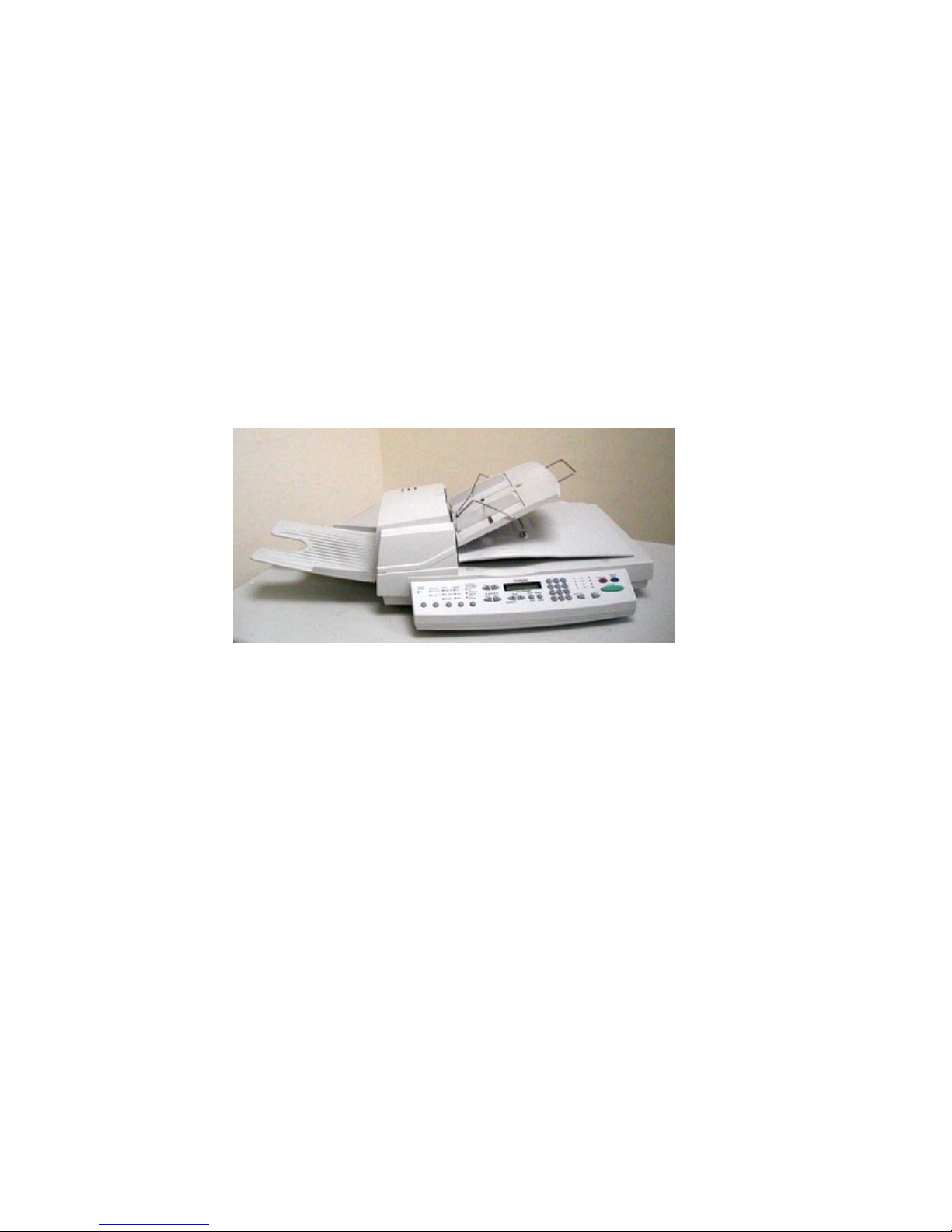
1.5 Device Configuration
This section describes the device configuration of the multifunction product.
Outer View
Extension
Auto Document
Feeder
Paper Feed
Tray
Document
cover
LCD-display
Control
Panel
Output
Paper Tray
Extension
1394 Port
Power Switch
Power Port
Figure 1.1 3200MFP Outer View
1-4

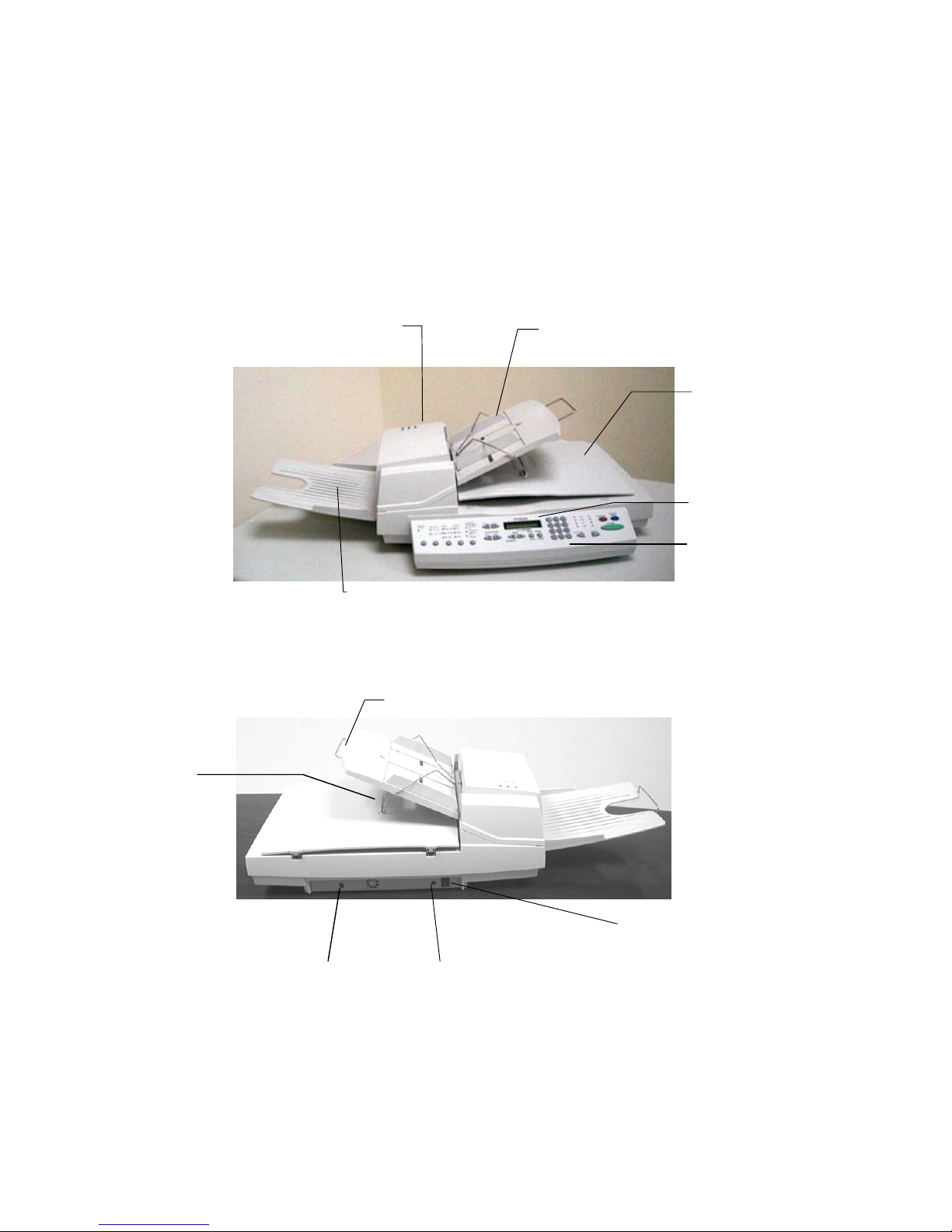
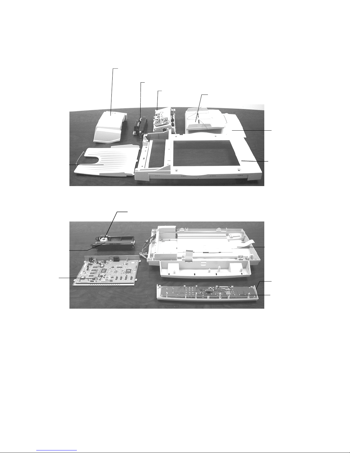
Mechanical Configuration
The equipment consists of the following components:
Image
Scanner
Document Cover
and Paper Tray
Upper Cover
ADF Unit
Lower Unit
Main Control
PCBA
Output Paper
Tray
Document Cover
ADF Paper Feed Tray
Upper Housing Unit
ADF Cover
Optical Chassis (ADF)
ADF Module
Bottom housing unit
Motor unit
Panel Cover
Panel PCBA
Optical Chassis (Flatbed)
1-5
ADF Cover
Optical Chassis (ADF)
ADF Module
ADF Paper Feed Tray
Document
Cover
Output
Paper Tray
Optical
Chassis
Main Control
PCBA
Upper
Housing Unit
Motor Unit
Bottom
Housing
Panel Cover
Panel PCBA
1-6
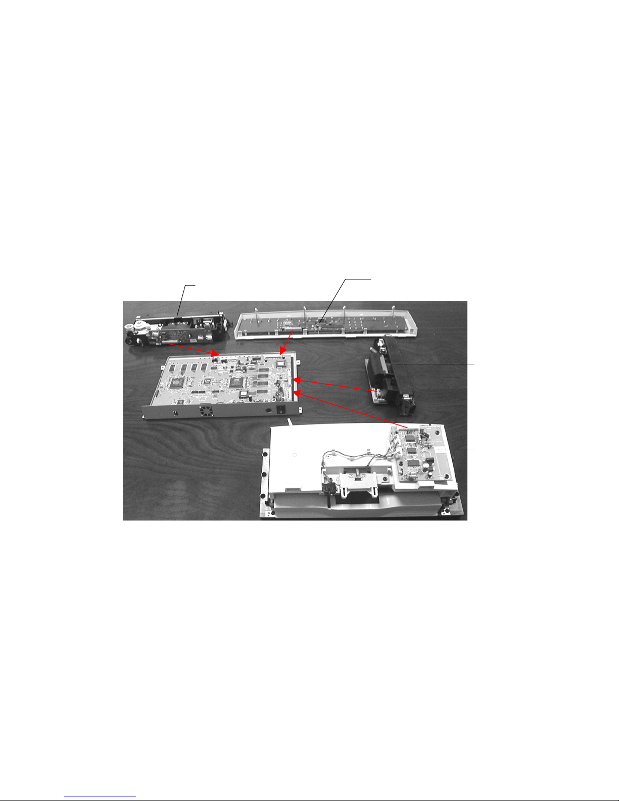
Wiring Configuration
CCD Board 1
Figure 1.2 Wiring Configuration
Control
Panel Board
CCD Board 2
LED Board
1-7

1.6 Theory of Operation
Introduction
This section explains the theory of operation of this scanner.
The microprocessor in this scanner controls the following functions.
• Interface
• Scanning module drive
• ADF drive
• Reading mode (reading density, document size, half-tone) selection.
Figure 1.3 shows the operation mode sequence.
Reading mode setting
ADF drive/scanning module drive Reading
Mechanical Section Operation
Scanning module drive
The carrier is driven by a 2-phase stepping motor. The stepping motor has a rotation of
1.8°(full step). And the use of micro-stepping control technique can work the motor to move
the scanning module at 1/300 inch/step.
ADF mechanism operation
The ADF is driven by a 2-phase stepping motor. The stepping motor has a rotation of 1.8°
(full step). The use of micro-stepping control technique enables the motor to move the paper
on the ADF at 1/300 inch/step.
Figure 1.3 Operation sequence
1-8

System Description
The 3200MFP is a duplex scanner which can scan synchronously both top and bottom size in a
document. It includes one main control board, two optical modules, one ADF module and one
LCD panel.
System Diagram
Figure 1.4 shows the system block diagram.
The main control board controls all the modules built up the 3200MFP. It includes a RISC.
ARM9(internal) as the main controller, one Flash Memory as program area , two ASIC for
flatbed and ADF image processing and each have external 64MB SRDRAM for data processing ,
two A/D converter for processing flatbed and ADF CCD signals input, two sets of motor
drivers for driving flatbed and ADF motors, one 1394 controller for data interfacing with
printer.
The power is an external 24V/2500mA power adapter for the whole system.
There are some different values inside the 3200MFP.
+24V Power directly comes from the power adapter and used for flatbed and ADF motor.
+12V Power converted from 7812 to supply flatbed and ADF CCD
+5V Power converter from 34063 to supply flatbed and ADF A/D converters and all 5V
logic.
+3.3V Power converted from LM 2576/3.3V to supply RTL8811, 1394 controller, two image
processing ASICs and some 3.3V logics.
1-9
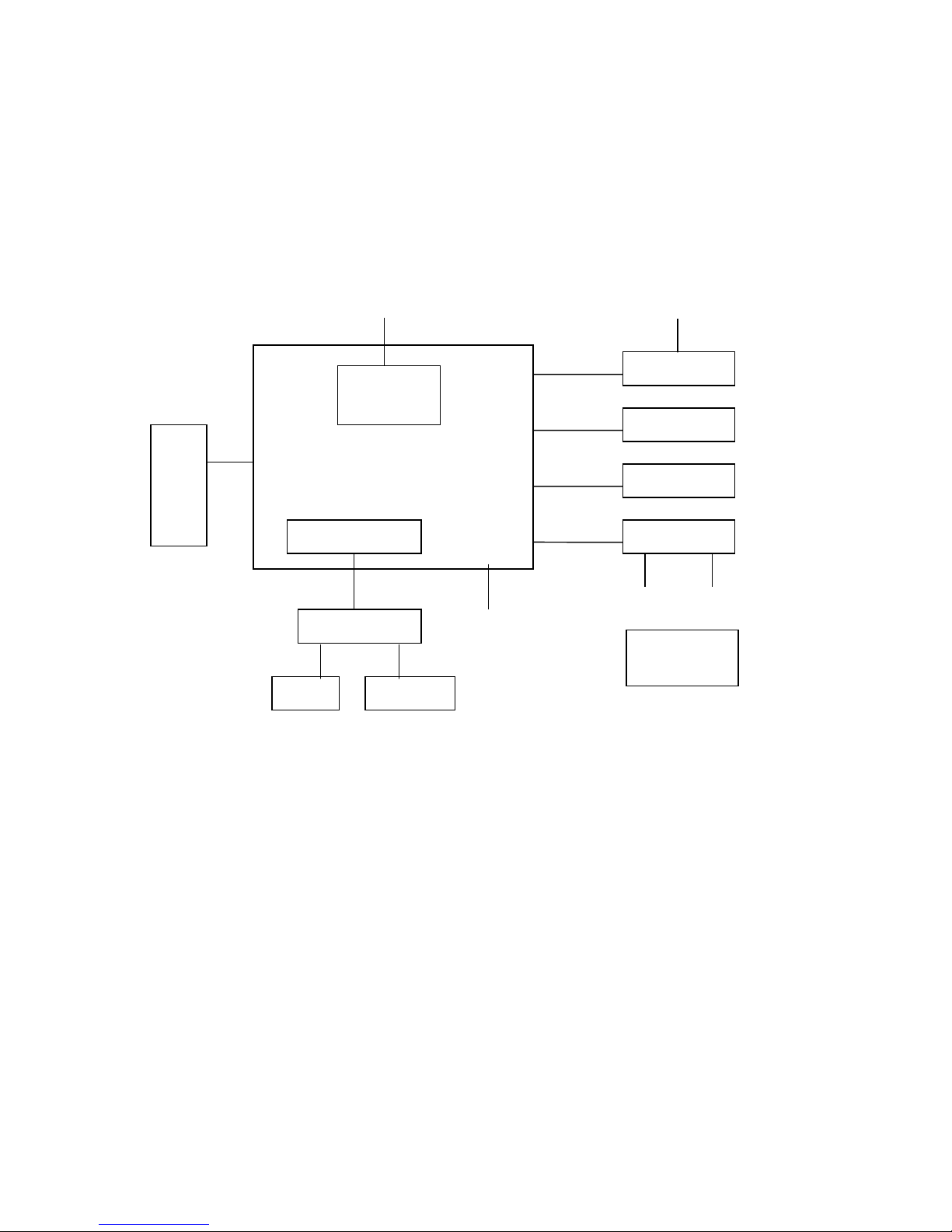
r
Control
Panel
To printer
1394
Controller
Main board
Control
section
110/240 VAC
Power supply
LED display
Sensor input
Video Circuit
Optical unit
Flatbed
moto
Lamp unitInverter
Figure 1.4 System Block Diagram
ADF section
ADF motor ADF sensor
ADF's video
circuit
1-10

1394 interface:
This scanner and the printer are connected via the 1394 interface.
Video circuit:
The video circuit of this scanner includes: CCD driving circuit, CCD signal processing circuit.
1 CCD Driving Circuit
Pin Assignment for Flatbed Video Circuit J3:
The CCD driving circuit is used to generate correct signals to the CCD, so that the CCD
may generate the correct image data.
Pin
Name Function
No.
1 H.G Inverter Ground
2 H.G Inverter Ground
4 Lamp V Inverter Power Supply
5 Lamp V Inverter Power Supply
6 +5V +5V Power Supply
7 SH Channel Shift Gate
8 Home Sensor Sensor Signal
9 D.G Digital Ground
10 PH2 CCD Clock Phase
11 PH1 CCD Clock Phase
12 D.G Digital Ground
13 Clamp CCD Clamp Signal
14 RS CCD Reset Gate
15 B/W CCD B/W Control Switch
16 +12V +12V Power Supply
17 VOR CCD red Channel Output Signal
18 A.G Analog Ground
19 VOG CCD Green Channel Output Signal
20 A.G Analog Ground
21 VOB CCD Blue Channel Output Signal
22 A.G Analog Ground
1-11
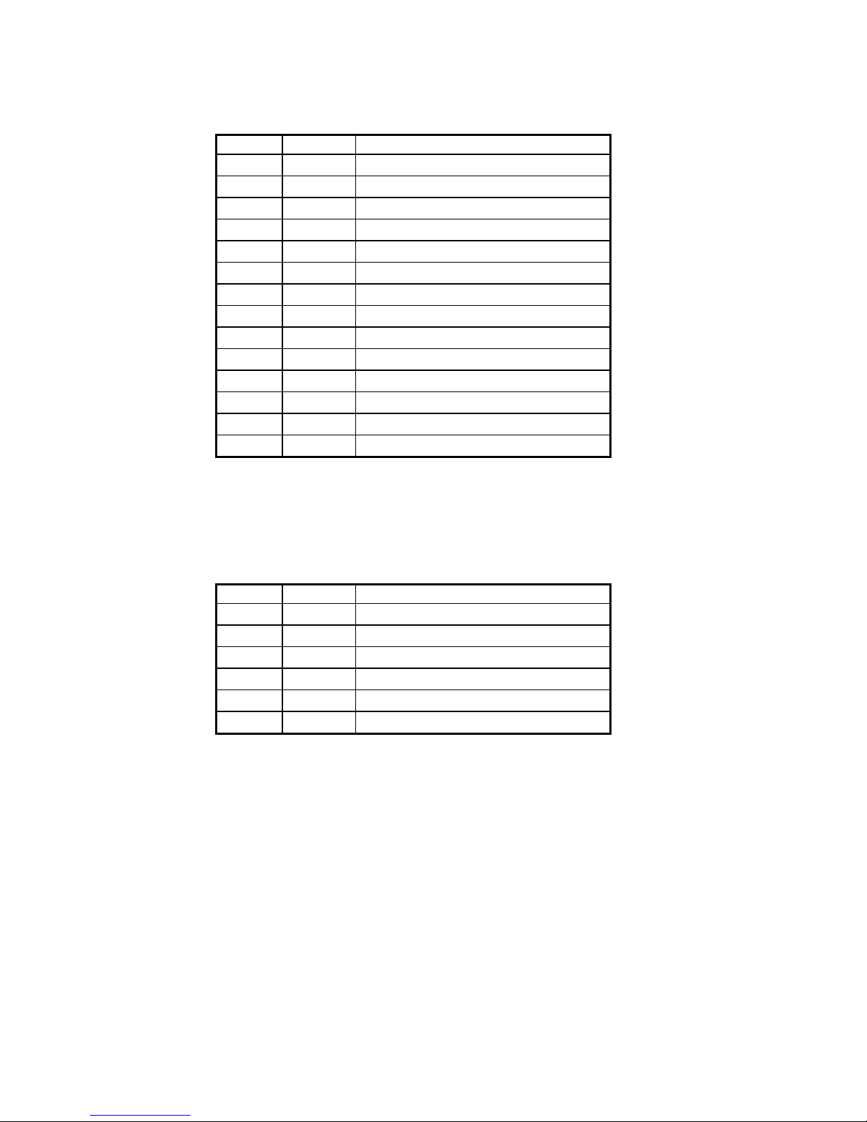
Pin Assignment for ADF Video Circuit J9:
Pin No. Name Function
1 H.G. Inverter Ground
2 +24V Analog +24V Power Supply
3 GND +5V GND
4 +5V +5V Power Supply
5 B/W CCD B/W Control Switch
6 SH Channel Shift Gate
7 RS CCD Reset Gate
8 Clamp CCD Clamp Signal
9 GND +5V GND
10 PH2 CCD Clock Phase
11 PH1 CCD Clock Phase
12 H24G +24V Ground
13 A.G Analog Ground
14 +24Va Analog +24Va Power Supply
Pin Assignment for ADF Video Circuit J8:
Pin No. Name Function
1 A.G Analog Ground
2 VOR CCD Red Channel Output Signal
3 A.G Analog Ground
4 VOG CCD Green Channel Output Signal
5 A.G Analog Ground
6 VOB CCD Blue Channel Output Signal
1-12

2. CCD signal processing circuit
R
CCD
G
B
MUX
Video Noise
Suppression
Circuit
PGA*
Level
Shift
A/D
Converter
DC Offset
Adjust Circuit
The video noise suppression circuit is to eliminate the reset noise and low frequency noise of
CCD and then PGA performs video gain control. The “level shift” circuit is used to bias the
PGA output to satisfy the reference bottom requirement of the A/D converter. The “DCOFFSET Adjust” circuit is used to adjust the bias level of video signal.
* PGA: Programmable gain amplifier
1-13
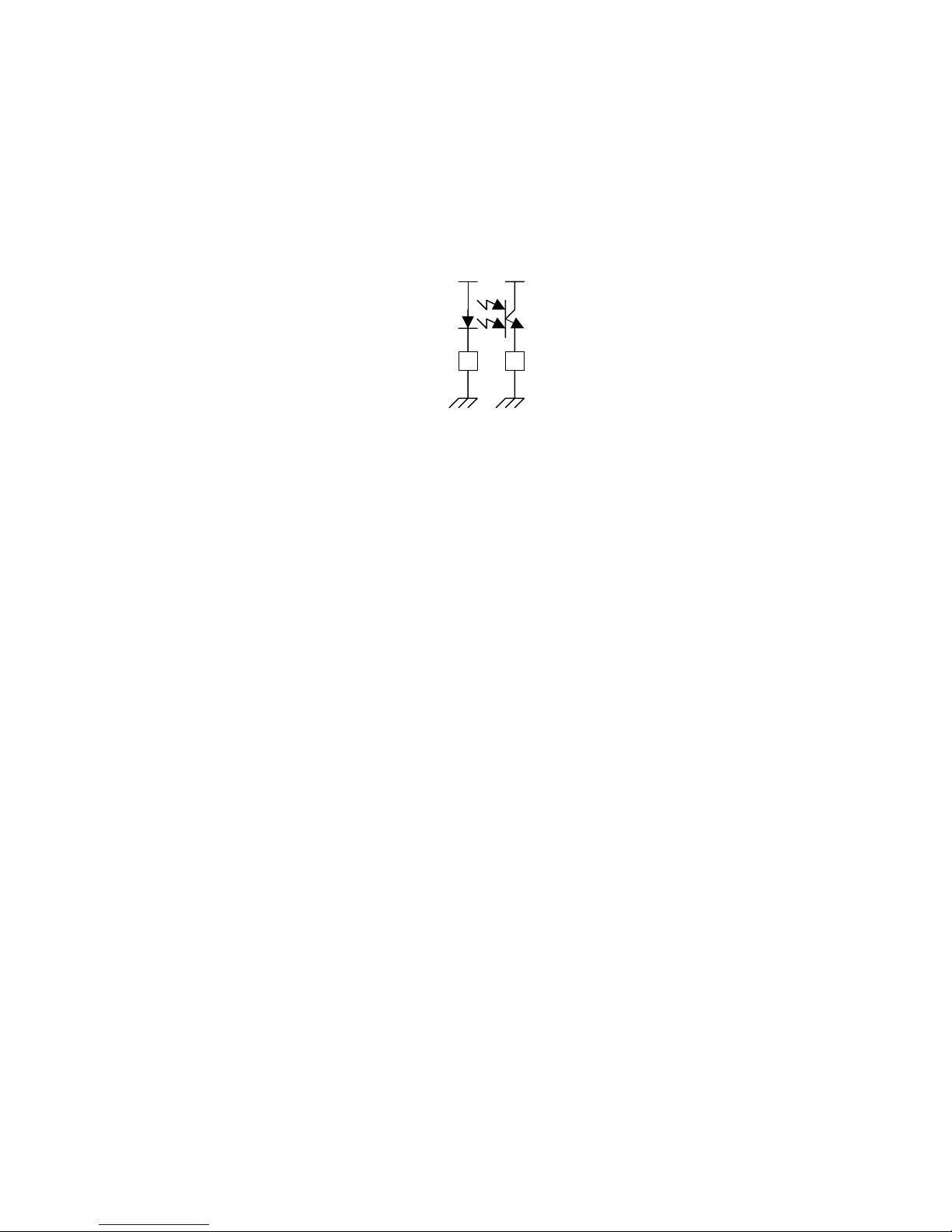
Sensor input
The sensor input includes home position sensor and ADF cover sensor.
1. Home position sensor
The home position is detected when the carrier passes between the LED and the photo transistor.
2. ADF cover sensor
The operation of the ADF cover sensor is the same as that of the home position sensor.
The home position of the carrier motor is detected by photo sensor. The photo
transistor transmission to the photo sensor receiver circuit is shown below .
+5V +5V
R R
Figure 1.5 Home position sensor
1-14

2. Installation
2.1 Precautions of Installation
2.2 Unpacking Procedure
2.3 Unlocking Your Scanner
2.4 Cable Connection
This chapter explains the unpacking procedure, installation procedure and confirmation of
operation.
2.1 Precautions of Installation
Pay attention to the following matters before unpacking and installation.
• Do not install in a place where vibration may occur.
• Keep the scanner out of direct sunlight. Do not install near a heat source.
• Do not place the scanner around materials which shut off the circulation of air.
• Do not install in a humid or dusty place.
• Do not use the wall socket with connecting devices which may generate noise, for example,
air-conditioner, etc.
• Use a suitable AC power source.
• Place the scanner on a level surface.
2.2 Unpacking Procedure
Unpack the scanner according to the following procedure.
• Remove the packing material.
• Remove the scanner from the shipping container.
• Remove the scanner from the PVC bag.
• Check the items
• For any missing items, please contact your nearest dealer or distributor.
2-1
2.3 Unlocking Your Scanner
The scanner is designed with the lock switch on the bottom to protect the scanning unit during
transportation. Please unlock the scanner first before using it.
1. Place the scanner on its side as shown in Figure 2.2
2. Locate the lock switch near the control panel. Move the lock switch to the "Unlock" position
as shown in Figure 2.3.
3. Remove the shipping retainer from its slot.
4. Insert the shipping retainer in the use position and fasten with the same screw as shown in Figure
2.3.
5. Place the scanner in its normal operating position.
Figure 2.2 Unlock the Scanning Unit
2-2
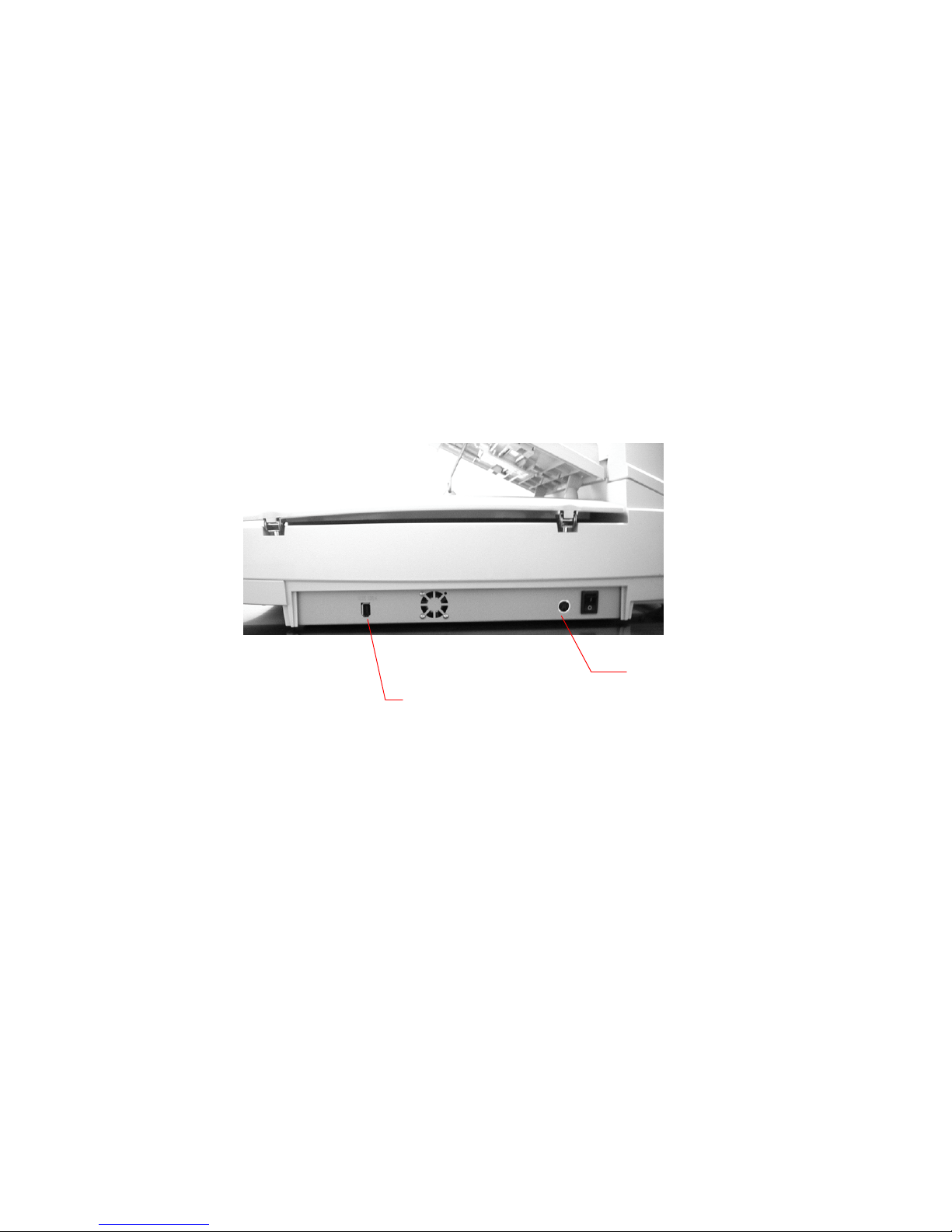
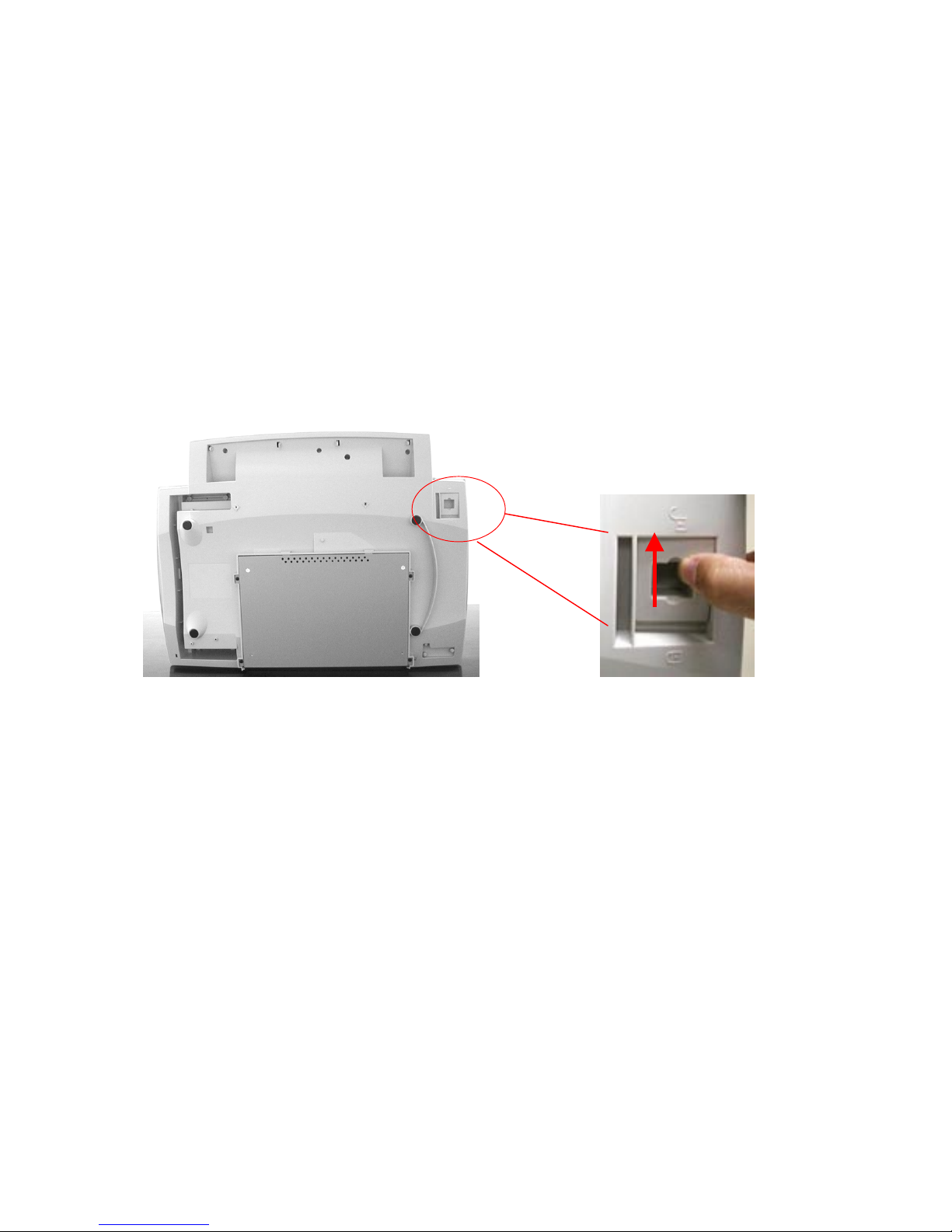
2.4 Cable Connection
Two cables are required to operate the scanner: the 1394 signal cable and the power cable. The
power cable connects the scanner to the power source. The 1394 signal cable connects the
scanner to the host for image transfer.
2.4.1 Power Cable Connection
1. Remove the power cable from the PVC bag.
2. Turn the power switch to the “off” position (“0” depressed).
3. Connect the female plug of the power cable to the scanner connector, and press it firmly
into place. (See Figure 2.4)
4. Connect the other end of the power cable to the power outlet, and press it firmly into
place.
1394 Port
Figure 2.4 Cable connection
Power Jack
2-3

 Loading...