

Lex Computech CI170A, CI170C User Manual

CI170A / CI170C
Intel ® Kaby Lake-S / Skylake-S Core™
I processor + Intel Q170,
DDR4 2133 MT/s / LAN / DVI / HDMI / DP
/ USB / PCIe mini card
All-In-One
6th / 7th gen. Intel Kaby Lake-S / Skylake-S Core™ I CPU
DVI, HDMI, LVDS, DP, LVDS (eDP), PCIe mini card
Multi-COM Board, Audio, LAN, SATA, USB
NO. CI170A/C
Release date: April 28th 2017

i
CI170A/C
Warning!...................................................................................................................................
Hardware Notice Guide ......................................................................................................
CHAPTER 1 GENERAL INFORMATION .................................................................................
1-1 MAJOR FEATURE................................................................................................................
1-2 SPECIFICATION ..................................................................................................................
1-3 INSTALLING THE CPU/PCH HEATSINK. (SOCKET VERSION) ........................................
1-4 VERTICAL SO-DIMM ASSEMBLY GUIDE ...........................................................................
1-5 INSTALLING THE MINI PCI-E CARD ..................................................................................
1-6 DIRECTIONS FOR INSTALLING THE MINI CARD .............................................................
1-7 PACKING LIST .....................................................................................................................
CHAPTER 2 HARDWARE INSTALLATION ............................................................................
2-1 UNPACKING PRECAUTION ................................................................................................
2-2 UNPACKING CHECKUP ......................................................................................................
2-3 DIMENSION-CI170A/C ........................................................................................................
2-4 FUNCTION MAP-CI170A/C .................................................................................................
2-5 CONNECTOR MAP-CI770A/C .............................................................................................
2-6 DIAGRAM-CI770A/C.............................................................................................................
2-7 NSTALL MEMORY ...............................................................................................................
2-8 LIST OF JUMPERS ..............................................................................................................
2-9 JUMPER SETTING DESCRIPTION .....................................................................................
2-10 JCMOS1: CMOS DATA Clear .............................................................................................
2-11 COM PORT PIN9 SELECT RI SIGNAL OR VOLTAGE SOURCE ......................................
2-12 JVP1: LVDS PANEL INVERTER POWER SELECT ...........................................................
2-13 JVL2: LVDS/eDP PANEL POWER SELECT ......................................................................
CHAPTER 3 CONNECTION ..................................................................................................
3-1 LIST OF CONNECTORS.......................................................................................................
3-2 DC 12V-IN EXTERNAL CONNECTOR .................................................................................
3-3 BATTERY INPUT ..................................................................................................................
3-4 DC POWER OUTPUT ..........................................................................................................
3-5 FRONT PANEL & FAN ..........................................................................................................
3-6 FAN CONNECTORS ............................................................................................................
3-7 DISPLAY & TOUCH INTERFACE .........................................................................................
3-8 HDMI INTERFACE ...............................................................................................................
3-9 EDP INTERFACE .................................................................................................................
3-10 LVDS INTERFACE .............................................................................................................
3-10-1 PANEL INVERTER POWER ...........................................................................................
3-11 TOUCH SCREEN DEVICE .................................................................................................
3-12 AUDIO INTERFACE ...........................................................................................................
Contents
1
2
4
5
6
7
9
10
11
12
13
13
14
15
16
17
18
19
20
20
21
22
24
24
25
25
26
27
28
28
30
31
32
33
34
35
36
37

ii
3-13 I/O INTERFACE ..................................................................................................................
3-14 DIGITAL INPUT / OUTPUT / WATCH DOG TIME ..............................................................
3-8-1 IO DEVICE: F75111 UNDER DOS ....................................................................................
3-8-2 IO DEVICE: F75111 UNDER WINDOWS ..........................................................................
3-8-3 IO DEVICE: F75111 VB6 UNDER WINDOWS ..................................................................
3-8-4 IO DEVICE: F75111 UNDER LINUX ..................................................................................
3-15 I
2
C BUS INTERFACE .........................................................................................................
3-15 LAN+USB INTERFACE ......................................................................................................
3-16 SATA INTERFACE ..............................................................................................................
3-17 MODULE SOCKET ............................................................................................................
3-18 SIM SOCKET .....................................................................................................................
3-19 SODIMM SOCKET .............................................................................................................
3-20 PCIe X16 GOLD FINGER PIN DEFINE ..............................................................................
CHAPTER 4 INTRODUCTION OF BIOS ................................................................................
4-1 ENTER SETUP ....................................................................................................................
4-2 BIOS MENU SCREEN .........................................................................................................
4-3 FUNCTION KEYS ................................................................................................................
4-4 GETTING HELP ...................................................................................................................
4-5 MENU BARS ........................................................................................................................
4-6 MAIN ....................................................................................................................................
4-7 ADVANCED ..........................................................................................................................
4-7-1 CPU CONFIGURATION ....................................................................................................
4-7-2 TRUSTED COMPUTING .................................................................................................
4-7-3 ACPI SETTINGS ...............................................................................................................
4-7-4 F81966 SUPER IO CONFIGURATION .............................................................................
4-7-4-1 ►SERIAL PORT 1 CONFIGURATION ..........................................................................
4-7-4-2 ►SERIAL PORT 2 CONFIGURATION ..........................................................................
4-7-4-3 ►SERIAL PORT 3 CONFIGURATION ..........................................................................
4-7-4-4 ►SERIAL PORT 4 CONFIGURATION ..........................................................................
4-7-4-5 ►SERIAL PORT 5 CONFIGURATION ..........................................................................
4-7-4-6 ►SERIAL PORT 6 CONFIGURATION ..........................................................................
4-7-6 F81216SEC SUPER IO CONFIGURATION .....................................................................
4-7-6-1 ►SERIAL PORT 1 CONFIGURATION ..........................................................................
4-7-6-2 ►SERIAL PORT 2 CONFIGURATION ..........................................................................
4-7-6-3 ►SERIAL PORT 3 CONFIGURATION ..........................................................................
4-7-6-4 ►SERIAL PORT 4 CONFIGURATION ..........................................................................
4-7-7 SERIALPORT CONSOLE REDIRECTION .......................................................................
4-7-8 INTEL TXT INFORMATION ..............................................................................................
4-7-9 NETWORK STACK CONFIGURATION ..........................................................................
4-7-10 CSM CONFIGURATION .................................................................................................
4-7-11 USB CONFIGURATION ..................................................................................................
39
42
43
45
51
55
60
61
65
66
67
69
70
73
73
74
74
75
75
75
76
77
77
78
79
80
81
82
83
84
85
86
86
87
88
89
90
90
90
91
91

iii
4-8 CHIPSET ..............................................................................................................................
4-8-1 SYSTEM AGENT (SA) CONFIGURATION ......................................................................
4-8-1-2 GRAPHICS CONFIGURATION ....................................................................................
4-8-1-3 PEG PORT CONFIGURATION ......................................................................................
4-8-2 PCH-IO CONFIGURATION ..............................................................................................
4-8-2-1 PCI EXPRESS CONFIGURATION ...............................................................................
4-8-2-1-1 PCI EXPRESS ROOT PORT 5/6/7/8 (I210/I211 LAN2/3/4/5) ....................................
4-8-2-2 SATA AND RST CONFIGURATION ..............................................................................
4-9 SECURITY ........................................................................................................................
4-10 BOOT ...............................................................................................................................
4-11 SAVE & EXIT ....................................................................................................................
CHAPTER 5 DRIVER INSTALLATION .................................................................................
5-1 INF INSTALL INTEL SKYLAKE CHIPSET DRIVER ...........................................................
5-2 VGA INSTALL INTEL LVY SKYLAKE VGA DRIVER ..........................................................
5-3 HD AUDIO INSTALL REALTEK HIGH DEFINITION AUDIO DRIVER ................................
5-4 ME TOOLS INSTALL INTEL MANAGEMENT ENGINE INTERGACE DRIVER .................
5-5 LAN INSTALL INTEL LAN DRIVER ...................................................................................
5-6 HOW TO UPDATE INSYDE BIOS ......................................................................................
APPENDIX A:POWER CONSUMPTION TEST ........................................................................
APPENDIX B:RESOLUTION LIST ...........................................................................................
92
93
94
95
96
97
98
99
100
101
102
103
105
106
107
108
110
113
115
116

Copyright
This manual is copyrighted and all rights are reserved. It does not allow any non
authorization in copied, photocopied, translated or reproduced to any electronic or
machine readable form in whole or in part without prior written consent from the
manufacturer.
In general, the manufacturer will not be liable for any direct, indirect, special, incidental
or consequential damages arising from the use of inability to use the product or
documentation, even if advised of the possibility of such damages.
The manufacturer keeps the rights in the subject to change the contents of this
manual without prior notices in order to improve the function design, performance,
quality, and reliability. The author assumes no responsibility for any errors or omissions,
which may appear in this manual, nor does it make a commitment to update the
information contained herein.
Trademarks
Intel is a registered trademark of Intel Corporation.
Award is a registered trademark of Award Software, Inc.
All other trademarks, products and or product's name mentioned here are for
identifi cation purposes only, and may be trademarks and/or registered trademarks
of their respective companies or owners.
© Copyright 2017
All Rights Reserved.
User Manual edition 0.1, April. 28th . 2017

1
Warning !
1. Battery
Batteries on board are consumables.
The life time of them are not guaranteed.
2. Fless solution with HDD
The specifi cation & limitation of HDD should be considered carefully when
the fanless solution is implemented.
3. We will not give further notifi cation in case of changes of
product information and manual.
4. SATA interface does not support Hot SWAP function.
5. There might be a 20% inaccuracy of WDT at room temperature.
6. Please make sure the voltage specifi cation meets the requirement
of equipment before plugging in.
7. Caution! Please notice that the heat dissipation problem could cause the MB
system unstable. Please deal with heat dissipation properly when
buying single MB set.
8. Please avoid approaching the heat sink area to prevent users from
being scalded with fanless products.
11. It is important to install a system fan toward the CPU to decrease
the possibility of overheating / system hanging up issues,
or customer is suggested to have a fi ne cooling system to dissipate heat
from CPU.
10. DO NOT apply any other material which may reduce cooling
performance onto the thermal pad.
9. If users repair, modify or destroy any component of product unauthorizedly,
We will not take responsibility or provide warranty anymore.

2
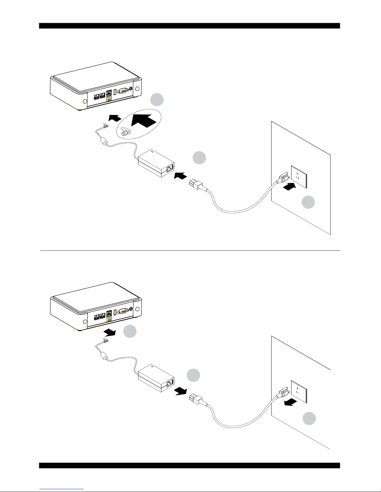
Hardware Notice Guide
1. Before linking power supply with the motherboard, please attach DC-in adapter to
the motherboard fi rst. Then plug the adapter power to AC outlet.
Always shut down the computer normally before you move the system unit or
remove the power supply from the motherboard. Please unplug the DC-in adapter fi rst
and then unplug the adapter from the AC outlet.
Please refer photo 1 as standard procedures.
2. In case of using DIRECT DC-in (without adapter), please check the allowed range
for voltage & current of cables. And make sure you have the safety protection for
outer issues such as short/broken circuit, overvoltage, surge, lightning strike.
3. In case of using DC-out to an external device, please make sure its voltage and
current comply with the motherboard specifi cation.
4. The total power consumption is determined by various conditions
(CPU/motherboard type, device, application, etc.). Be cautious to the power cable
you use for the system, one with UL standard will be highly recommended.
5. It’s highly possible to burn out the CPU if you change/ modify any parts of
the CPU cooler.
6. Please wear wrist strap and attach it to a metal part of the system unit
before handling a component. You can also touch an object which is
ground connected or attached with metal surface if you don't have wrist strap.
7. Please be careful to handle & don't touch the sharp-pointed components on
the bottom of PCBA.
8. Remove or change any components form the motherboard will VOID the warranty of
the motherboard.
9. Before you install/remove any components or even make any jumper setting
on the motherboard, please make sure to disconnect the power supply fi rst.
(follow the aforementioned instruction guide)
10. "POWERON after PWR-Fair” function must be used carefully as below:
When the DC power adaptor runs out of power, unplug it from the DC current;
Once power returns, plug it back after 5 seconds.
If there is a power outage, unplug it from the AC current, once power returns,
plug it back after 30 seconds. Otherwise it will cause system locked or made
a severe damage.
Remark 1:
Always insert/unplug the DC-in horizontally & directly to/from the motherboard.
DO NOT twist, it is designed to fi t snugly.
Moreover, erratic pull / push action might cause an unpredictable damage to the
component & system unit.
*
3
2
1
3
1
2
3
Photo 1 Insert
Unplug

4
Chapter-1
General Information
The CI170A/C is an All-In-One board which is 7th/6th Gen Intel® Core™ i7/i5/i3 and
Pentium®/Celeron® Processor (formerly codenamed Skylake-S) based industrial
motherboard in the LGA1151 package with Intel® Q170 Express chipset. The CI170A/C
supports high-speed data transfer interfaces such as PCIe3.0, USB 3.0, and SATA 6 Gb/s
(SATA III), with dual-channel DDR4 2133 MHz memory up to 32 GB in two SO-DIMM slots
and supports 4 USB 3.0, 5 USB 2.0, 10 COM and 4 SATA III ports, as well as graphics
interface for DVI-D, HDMI and DisplayPort displays.
High-performance and power-efficient communication platform, the embedded
motherboard of CI170A/C is specially designed for IoT, industrial, digital signage, medial,
POS, retail and factory automation applications.CI170A/C with a wide variety of expansion
options including PCIe(x16), PCIe(x8), PCIe(x4), PCIe(x1), or 2 PCIe(x8), 2 PCIe(x4), 2
PCIe(x1), selectable by raiser cards. The platform comes with fi ve Intel Gigabit Ethernet
controllers and supports Wake-On LAN, vPro with TPM 2.0 and the PXE function in BIOS
for Intel LAN chipset, it is perfect control board for networking devices.
The CI170A/C also supports up to ten of serial ports RS232/RS422/RS485 auto switch
by BIOS settings and +5V/12V selectable by jumper. In addition, there are multi-ports of
Hi-Speed USB 3.0/2.0 to enhance the host controller interface which will ensure the high
performance level and fl exible expansion. The expandable interfaces include 1 full-size
PCIe Mini card for PCIe x 1 or mSATA (auto-detection) and USB interface, and 1 full-size
PCIe Mini card for PCIe x 1 and USB interface. There are two SIM socket onboard for the
mini cards to get the 3G/4G communication easier and quickly.
The CI170C supports LVDS interface and touch controller onboard for touch panel and
1 panel inverter power for panel dimming control. It suitable for ALL-IN ONE Panel PC,
POS, Kiosk and automation control systems. The All-In-One motherboard 3I385AW/CW
is fully compatible with industry standards, plus technical enhancements and thousands
of software applications developed for IBM PC/AT compatible computers. These control
logic provides high-speed performance for the most advanced multi user and multitasking
applications available today.

5
1. The Desktop Skylake S-Platform processor includes Integrated Display Engine, GPU
and Integrated Memory Controller. The processor is designed be offered in a LAG1151 package.
2. Intel Q170 Chipset Family Platform Controller Hub (PCH)
3. Supports Two Channels of DDR4 SO-DIMM SDRAM, Max. 32GB, data transfer rates of
1866MT/s and 2133 MT/s
4. Intel Desktop Skylake S-Platform Processor Integrated Graphics. GEN 9 architecture supports
up to 72 Execution Units (EUs), depending on the processor SKU.
5. Integrated Gigabit LAN Controller with Intel I219LM Gigabit Ethernet PHY supports
vPro. *1 Support 4 x 10/100/1000 Mbps Intel LAN ports.*2
6. Support DP, HDMI, DVI eDP1.3 2 lanes &18/24 bits dual channel LVDS Interface on Board. *3
7. Support 10 x RS232 auto switch to RS485/RS422 by BIOS, 4 port external, 6 port internal. *4
8. 4 x type A USB3.0 external and 5 x USB 2.0 internal
9. ALC886 HD Audio Specifi cation 1.0 Two channels sound. Two channel Class D Audio Amplifi er. *5
10. Four SATA ports 3.0 Data transfer rates up to 6.0 Gb/s (600 MB/s)
11. Support extended 1 x Mini PCIe card for PCIe x 1, mSATA and USB interface, 1 x Mini PCIe card
for PCIe x 1 and USB interface. There are 2 x SIM Card Socket for these two mini cards.
(3G/4G LTE module)
12. One M.2 B-Key 2242 for PCIe & mSATA devices
13. USB touch screen controller for CI170C only
14. Hardware digital Input & Output, 8 x DI / 8 x DO, Hardware Watch Dog Timer, 0~255 sec
programmable
15. PCIe x 16 Golden Finger supports 1 PCIe x 1, 4, 8,16 or 2 PCIe x 1, 4, 8 with Riser Cards
16. Support TPM 2.0 *6
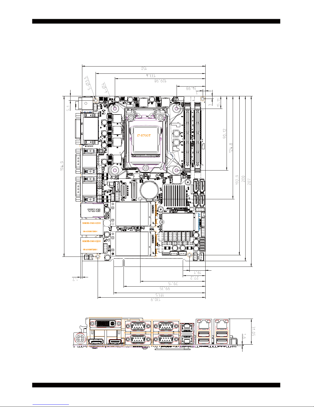
17. PCB Dimension: 200 x 150 mm
*1 & *6 CI170C only
*2 CI170A supports 2 LAN ports
*3 eDP & LVDS shared the same signal, LVDS for CI170C only
*4 CI170A supports 6 COM
*5 Audio Amplifi er for CI170C only
1-1 Major Feature

6
1. CPU: Desktop Skylake S-Platform processor. The processor is designed be offered
in a LAG1151 package.
2. Memory: Two SO-DIMM slots for DDR4 SDRAM, Max. 32GB, data transfer rates of
1866MT/s and 2133 MT/s
3. Graphics: Intel Desktop Skylake S-Platform Processor Integrated Graphics.
GEN 9 architecture supports up to 72 Execution Units (EUs), depending on the
processor SKU. eDP 1.3 2 Lanes up to 1920 x 1200, DVI 1.2 2048 x 1080, DP 1.2
4096 x 2160, HDMI 1.3 up to 3840 x 2160
4. SATA: Integrated Serial ATA Host Controller Up to 4 SATA port, SATA Gen3 Data
transfer rates up to 6.0 Gb/s (600 MB/s).
5. LAN: Intel I210-AT LAN chipset or Intel I211-IT LAN chipset (Option) with
10/100/1000 Mbps
6. I/O Chip: Chipsets for 10 ports RS232/422/485
7. USB: 4 type A USB 3.0 connector onboard and 6 USB 2.0 (internal)
8. Sound: Support line in, line out and MIC in, Audio Amplifi er: Ti TPA2012D2RTJ
Class D 2.1W Audio amplifi er
9. LVDS: support 24bits/2ch LVDS interface
10. WDT/DIO: Hardware digital Input & Output, 8 x DI / 8 x DO / Hardware Watch Dog
Timer, 0~255 sec programmable
11. Expansion interface: one full-size PCIe Mini card for PCIe x 1, mSATA and USB
interface, one full-size Mini PCIe card for PCIe x 1 and USB interface with 2 SIM
sockets. 1 M.2 for mSATA or PCIe devices.
12. Touch screen: C8051F321 USB interface touch screen controller, support 4-, 5-, 8-
wire Analog resistive touch screen
13. Golden Finger: PCIe x 16 Golden Finger supports 1 PCIe x 1, 4, 8,16 or 2 PCIe x 1,
4, 8 with Riser Cards
14. TPM: Infi neon SLB 9665 TT 2.0 Trusted Platform Module
15. BIOS: AMI UEFI BIOS
16. Dimension: 200 x 150 mm
17. Power: DC IN +12V
1-2 Specifi cation
7
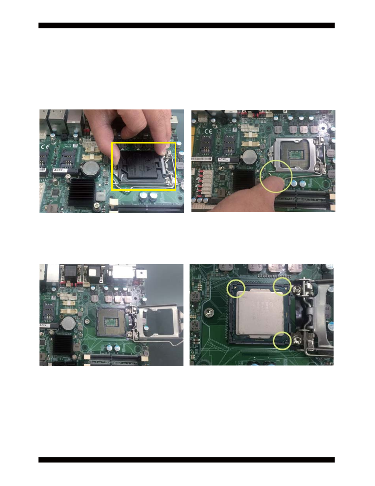
1-3 Installing the CPU / PCH Heatsink. (Socket Version)
1. Install CPU bracket under the CPU fi rst.
2. Use screw driver and screw the socket
screw in anti-clockwise direction.
2.1. Locate Pin1 in the socket,look for a
golden narrow.
2.2. Lock the CPU socket by securing the
screw in an anti-clockwise direction .
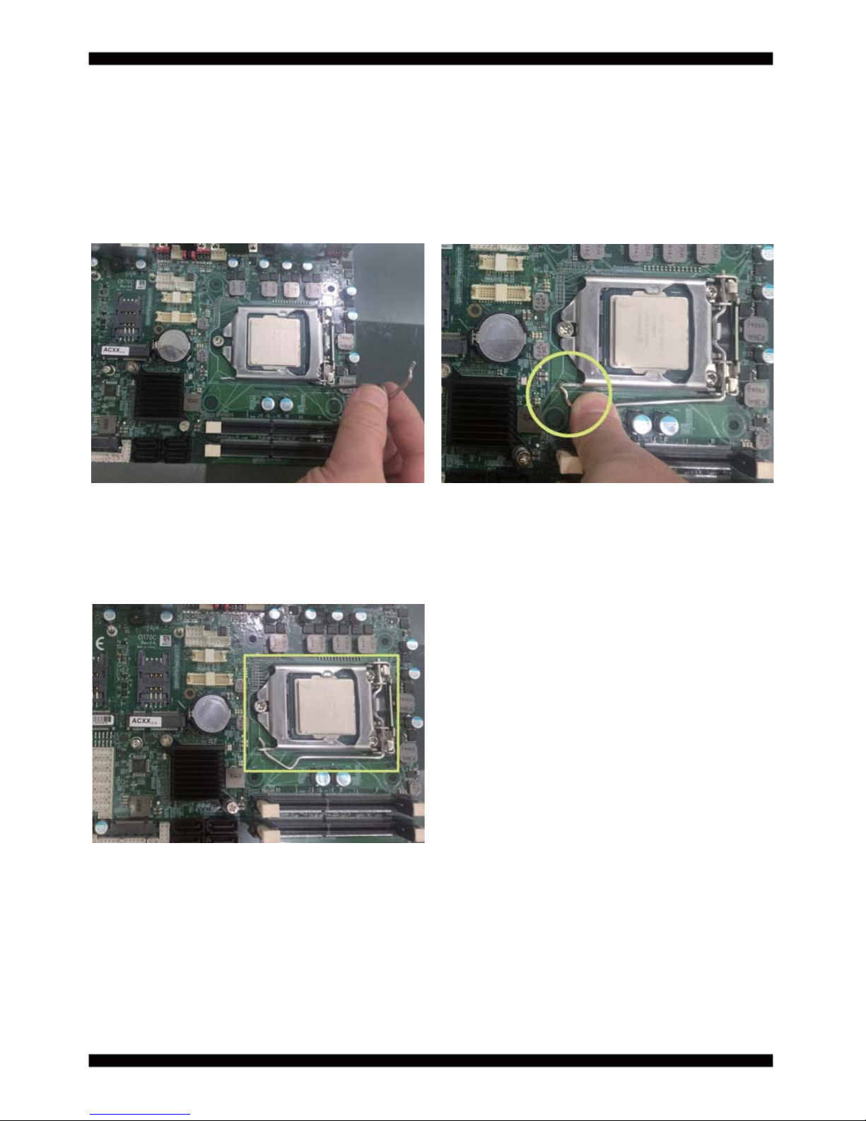
8
3. Peel-off the Elastic Silicone sticker
under the Heat Sink.
3.2 Insert the system fan power cable to
the pin header (FAN1) on board.
3.1 Tighten the HEAT SINK on the motherboard.
Pay attention to tighten the screws diagonally.
9
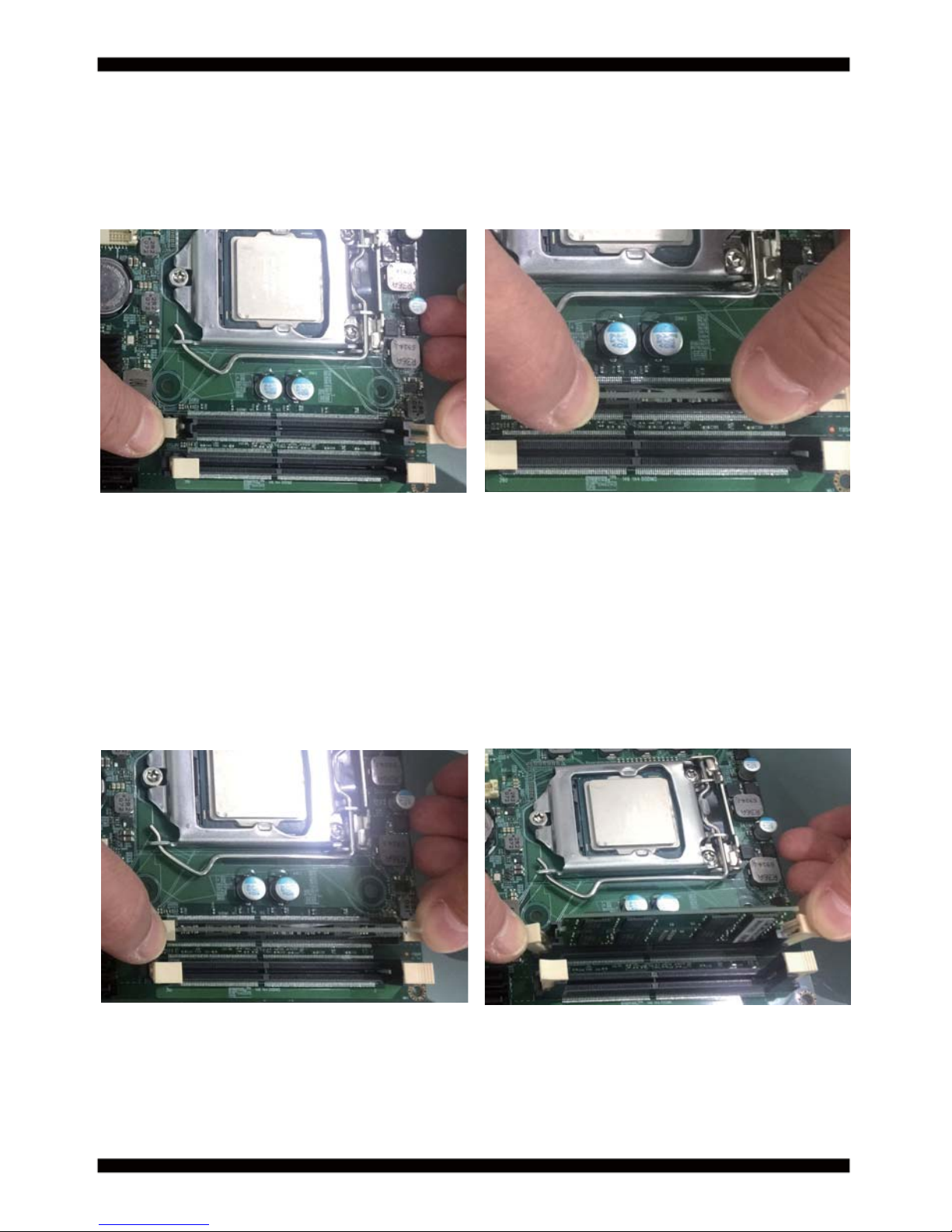
1-4 Vertical SO-DIMM assembly guide
1. Install the memory into SODIMM. 2. Press down fi rmly to ensure the memory
is locked.
1. Pull open both sides of the memory slot. 2. Take out the memory.
Uninstall
------------------------------------------------------------------------------------------------------------------------
10
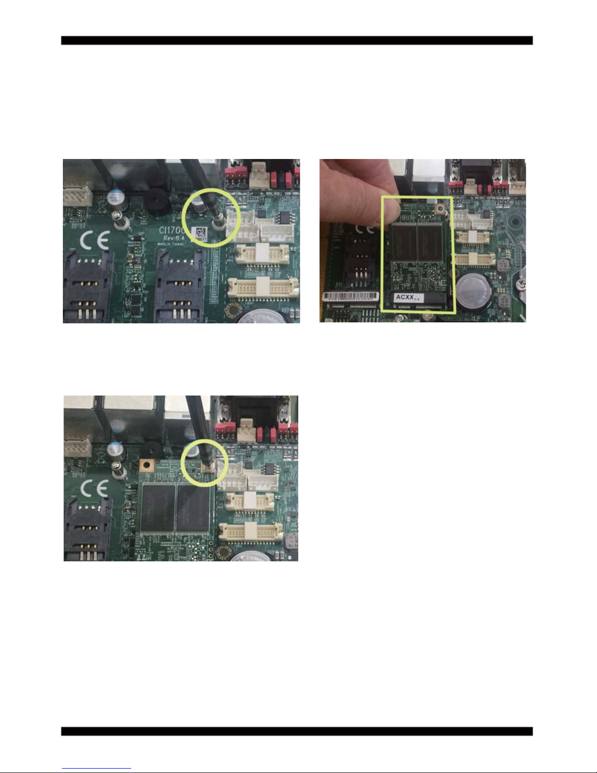
1. Unscrew the screw on the board
3. Gently push down the Mini Card and screw the screw back.
2. Plug in the Mini Card in a 45 angle
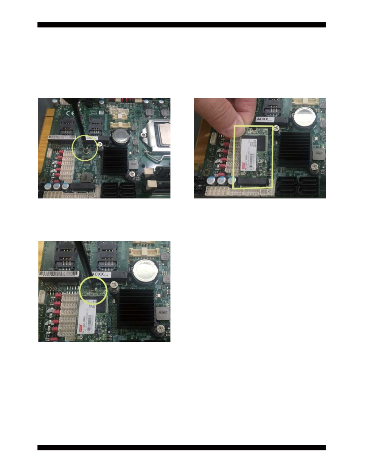
1-5 Directions for installing the Mini Card
11
1. Unscrew the screw on the board
3. Gently push down the Mini Card and screw the screw back.
2. Plug in the Mini Card in a 45 angle
1-6 Directions for installing the Mini PCI-e Card (Full Size)
12
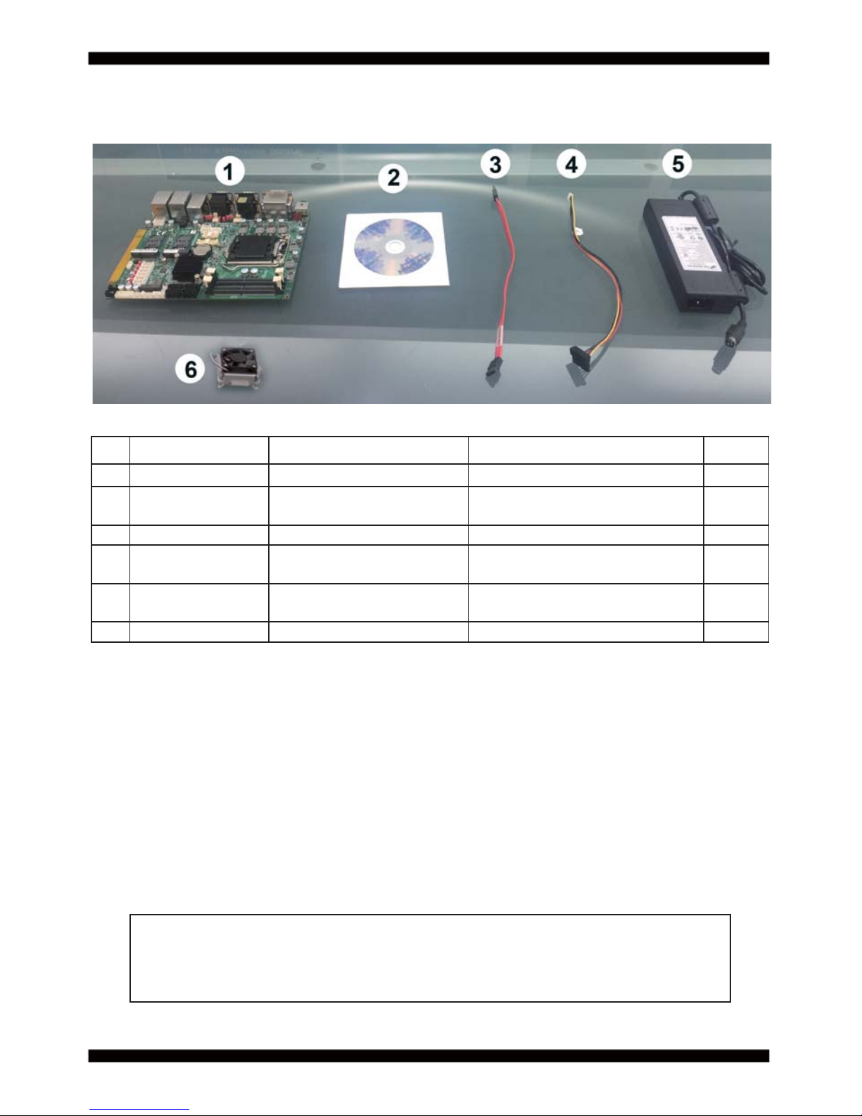
1-7 Packing List
Material Code Description Detail Specifi cation Quantit
1 7G1901-1650001-0 MB-CI170C-ACXX-001 LF, CI170C-ACXX, Rev.:001 1
2 6G8006-2349-0100 LEX Product Driver DVD
LF, Intel Baytrail Driver, Windows
7/8.1 32/64
1
3 6G6001-2203-0100 SATA DATA Cable (Red) LF, L=25cm 1
4 6G6003-1009-0100 SATA Power Cable
LF, L=25cm,
1*5/2.0 to 180° SATA 15p
1
5 6G6003-1009-0100 120W Power Adapter,12V
LF, M4P/Lock, FSP120-AHAN1,
FSP
1
6 COOLER 1
*The packing list above is for the users who purchase single motherboard. The users
who purchase the board with chassis may refer to the packing list in the Assembly Guide.
Please contact with your dealer if any of these items is missing or damaged
on delivery. And please keep all parts of the delivery package with packing
materials in case if you need to deliver or store the product in the future.

13
Chapter-2
This chapter provides the information how to install the hardware of CI170A/C.
Please follow section 1-7, 2-1 and 2-2 to check the delivery package and unpack
carefully. Please follow the jumper setting procedure.
You should follow these
steps to protect the board from the static electric
discharge whenever you handle the board:
1. Ground yourself by a grounded wrist strap at all times when you
handle the CI170A/C.
Well secure the ALLIGATOR clip of the strap to the end of the shielded wire lead from
a grounded object. Please put on and connect the strap before handling the
CI170A/C for harmlessly discharge any static electricity
through the strap.
2. Please use anti-static pad to put any components, parts, or tools on the pad whenever
you work on them outside the computer. You may also use the anti-static bag instead of
the pad. Please ask your local supplier for necessary parts on anti-static requirement.
3. Do not plug any connector or set any jumper when the power is on.
Hardware Installation
2-1 Unpacking Precaution
NOTE!
1. Do not touch the board or any other sensitive components without all necessary
anti-static protection.
2. Please pay attention to the voltage limitation of DC-IN12V 5%.
Overuse of DC-IN voltage limitation or change to another power adapter
(not provided with this system) will VOID warranty.

14
First of all, please follow all necessary steps of section 2-1 to protect CI170A/C
from electricity discharge. With reference to section 1-7
please check the delivery package again with following steps:
1. Unpack the CI170A/C board and keep all
packing material, manual and driver disc etc, do not dispose !
2. Is there any components lose or drops from the board?
DO NOT CONTINUE TO INSTALL THIS BOARD!
CONTACT THE DEALER YOU PURCHASED
THIS BOARD FROM, IMMEDIATELY.
3. Is there any visible damage on the board?
DO NOT CONTINUE TO INSTALL THIS BOARD!CONTACT
THE DEALER YOU PURCHASED THIS BOARD FROM, IMMEDIATELY.
4. Check your optional parts (i.e. DDR, CF etc.), all necessary jumpers
setting to jumper pin-set, and CMOS setup correctly.
Please also refer to all information of jumper settings in this manual.
5. Check your external devices (i.e. Add-On-Card, Driver Type etc.)
for complete add-in or connection and CMOS setup correctly.
Please also refer to all information of connector connection in this manual.
6. Please keep all necessary manual and driver disc in a good condition for future
re-installation if you change your Operating System.
2-2 Unpacking checkup
15
2-3 Dimension-CI170A/C
16
2-4 Function MAP-CI170A/C
DC 12V IN
LAN 3
USB3.0/2.0
LAN 5
DVI
LAN 4
COM 1~4
LAN 2
Front Panel
PCIe/USB
DDR4 SO-DIM
PS2 KB/MS
SMBUS
5 x USB2.0
8 DI/DO
USB Touch
CPU FAN
SIM 1
4 x SATA
Line-out
/Line-in/Mic-in
Audio AMP-L/R
DC-IN
SIM 2
System FAN
CPU Socket
M.2 B Key
+12V/+5V output
LAN1
LVDS
eDP
LCD Power
Auto Detect/
USB/mSATA
COM5~10(RS232/422/485)
Display port
HDMI
(RS232/422/485)

17
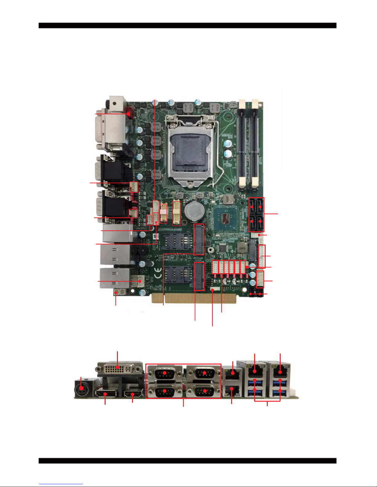
2-5 Connector MAP-CI170A/C
CPI12
CPI1
DP1
DVI1
HDMI1
CC1&2
FAN2
JVC1
JVC2
JVP1
JVL1
JVL2
FAN1
CC3&4
JVC3
JVC4
CL4&5
CUL3
CUL2
CAL1
CAR1
CA1
CL1
CT1
SIM2
SIM1
MPCE2
MPCE1
JVC5
JVC6
CKM1
CSP2(OEM)
CSP1(OEM)
JVC7
JVC8
JVC9
JVC10
CPO1
CPO2
CU5
CU4
CU3
CU2
CU1
CIO1
CO1
CIO2
NGFF1
SWP1
CFP1
SATA3
SATA4
SATA1
SATA2
SODIM1
SODIM2
CC5
CC6
CC7
CC8
CC9
CC10
JCMOS1
CPU1
LVDS1
EDP1
CPP1
CL11

18
2-6 Diagram-CI170A/C
CPI12
CPI1
DP1
DVI1
HDMI1
CC1&2
FAN2
JVC1
JVC2
JVP1
JVL1
JVL2
FAN1
CC3&4
JVC3
JVC4
CL4&5
CUL3
CUL2
CAL1
CAR1
CA1
CL1
CT1
SIM2
SIM1
MPCE2
MPCE1
JVC5
JVC6
CKM1
CSP2(OEM)
CSP1(OEM)
JVC7
JVC8
JVC9
JVC10
CPO1
CPO2
CU5
CU4
CU3
CU2
CU1
CIO1
CO1
CIO2
NGFF1
SWP1
CFP1
SATA3
SATA4
SATA1
SATA2
SODIM1
SODIM2
CC5
CC6
CC7
CC8
CC9
CC10
JCMOS1
CPU1
LVDS1
EDP1
CPP1
CL11
19
2-7 Install Memory
Valid Memory Confi gurations
Please refer to page 9 for installation of memory module.
DIMM1 / 2
NOTE!
System Accept or Not
Total Memory
DS Accept
Max.
16GB
This motherboard provides one 260-pin Small Outline Dual In-line Memory Module (SODIMM)
socket for memory expansion available maximum to of 4GB/8GB/16GB DDR4 SDRAM.
DDR4 clock supports: DDR4 1866/2133MT/S
The detected memory size is less than actual installed memory size since
some memory has been allocated for system use.
That’s how PC works with system memory.
20
JCMOS1: CMOS clear select
JVC1: COM1 voltage select
JVC2: COM2 voltage select
JVC3: COM3 voltage select
JVC4: COM4 voltage select
JVC5: COM5 voltage select
JVC6: COM6 voltage select
JVC7: COM7 voltage select
JVC8: COM8 voltage select
JVC9: COM9 voltage select
JVC10: COM10 voltage select
JVP1: LVDS Panel Inverter power select
JVL2: LVDS/eDP Panel power select
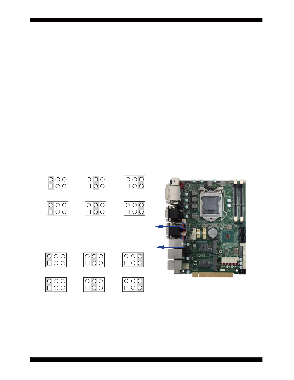
2-8 List of Jumpers
2-9 Jumper Setting Description
A jumper is ON as a closed circuit with a plastic cap covering two pins. A jumper is OFF
as an open circuit without the plastic cap. Some jumpers have three pins, labeled 1, 2,
and 3. You could connect either pin 1 and 2 or 2 and 3.The below fi gure 2.2 shows the
examples of different jumper settings in this manual.
All jumpers already have its default setting with the plastic cap inserted as ON,
or without the plastic cap as OFF. The default setting may be referred in this
manual with a " * " symbol .
Figure 2.2
21
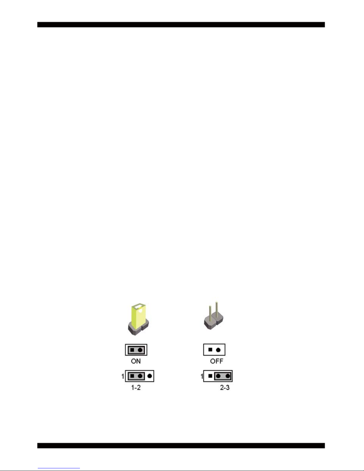
2-10 JCMOS1: CMOS DATA Clear
Note: Normal work is open jumper
JCMOS1
Note: Do not clear CMOS unless
1. Troubleshooting
2. Forget password
3. You fail over-clocking system
JCMOS1 Description
*1-2 Normal set
short CMOS data clear
A battery must be used to retain the motherboard confi guration in CMOS RAM.
Close Pin1 and pin 2 of JCMOS1 to store the CMOS data.
To clear the CMOS,follow the procedures below:
1. Turn off the system and unplug teh AC power
2. Remove DC IN power cable from DC IN power connector
3. Locate JCMOS1 and close pin 1-2 for few seconds
4. Return to default setting
5. Connect DC IN power cable back to DC IN Power connector
112233
*Normal
CMOS
22
2-11 COM port pin9 select RI signal or Voltage source
JVC1: COM1 PIN9 select JVC2: COM2 PIN9 select
JVC3: COM3 PIN9 select JVC4: COM4 PIN9 select
JVC5: COM5 PIN9 select JVC6: COM6 PIN9 select
JVC7: COM7 PIN9 select JVC8: COM8 PIN9 select
JVC9: COM9 PIN9 select JVC10: COM10 PIN9 select
JVC1/2/3/4/5/6/7/8/9/10 DESCRIPION
*1-2 COM port pin9 use RI signal
3-4 COM port pin9 use +5V voltage
5-6 COM port pin9 use +12V voltage
Note: 1.Attention! Check Device Power in spec
2.If want to use +5V/+12V need check system power design spec
*RI Signal
+5V
+12V
135
462
JVC3
JVC4
135
462
135
462
462462
462
135 135
135
*RI Signal
+5V
+12V
135
462
JVC1
JVC2
135
462
135
462
135 135
135
462462
462
23
*RI Signal
+5V
+12V
315
JVC5
642
315
642
315
642
315
642
315
642
315
642
JVC6 JVC7
JVC8
JVC9
JVC10
315
JVC5
642
315
642
315
642
315
642
315
642
315
642
JVC6 JVC7
JVC8
JVC9
JVC10
315
JVC5
642
315
642
315
642
315
642
315
642
315
642
JVC6 JVC7
JVC8
JVC9
JVC10
24
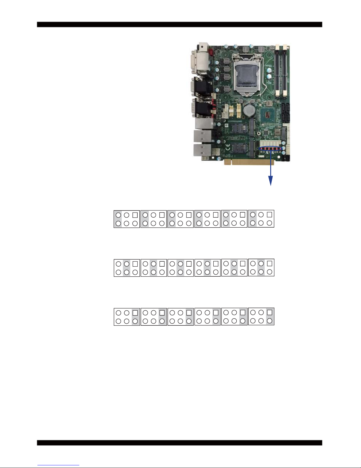
2-12 JVP1: LVDS panel Inverter power select
Note : Attention ! Check Device Power in spec.
JVP1 Description
1-2
+12V
*2-3
+5V
JVP1
132
+12V *+5V
132
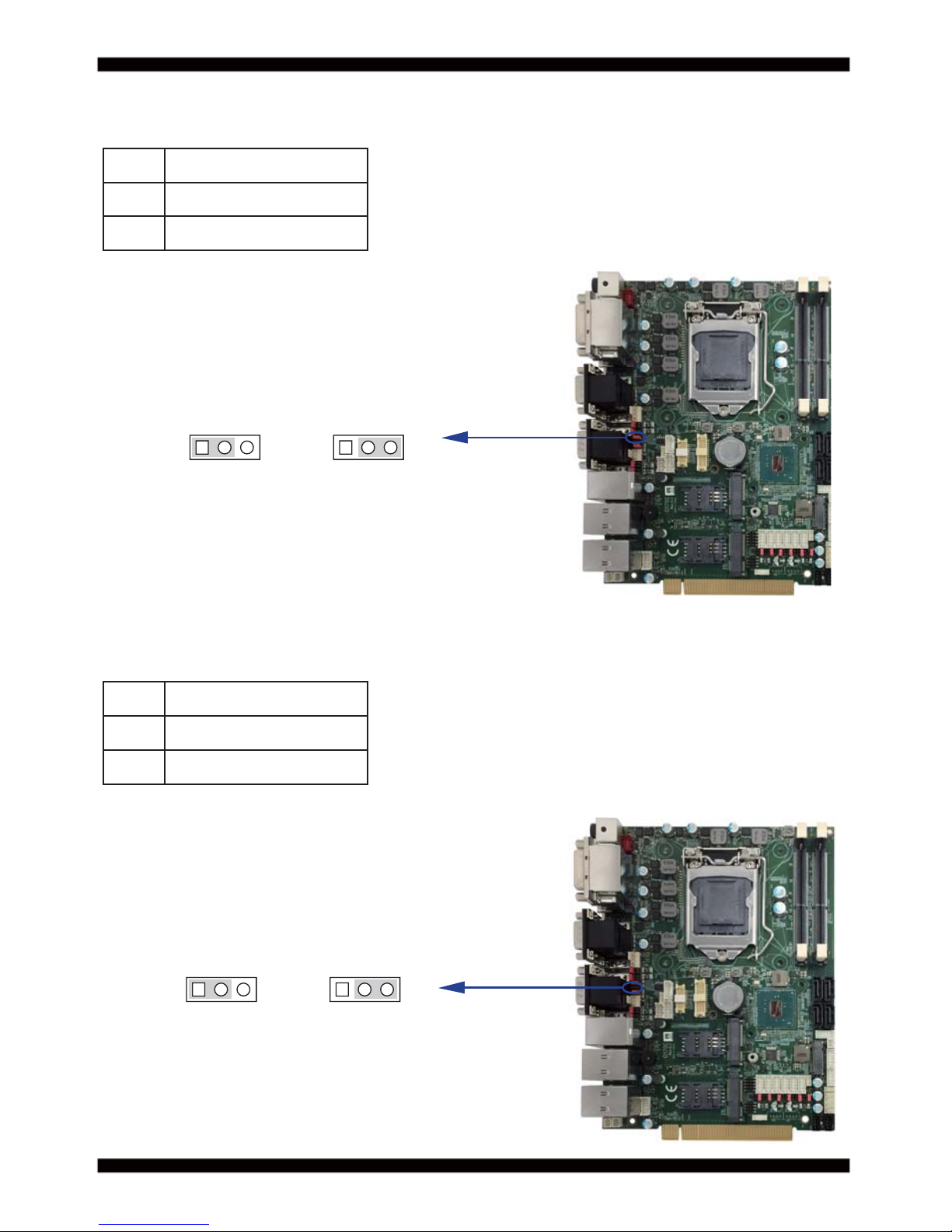
2-13 JVL2: LVDS/eDP panel power select
Note : Attention ! Check Device Power in spec.
JVL2 Description
1-2
+5V
*2-3
+3.3V
JVL2
+5V *+3.3V
132
132

25
Chapter-3
3-1 List of Connectors
Connection
This chapter provides all necessary information of the peripheral's connections,
switches and indicators. Always power off the board before you install the peripherals.
CPI1: DC 12V-in DIN external connector (4pin mini din connector)
CPI12: DC-in 2x4 pin (2.00mm) Red wafer connector
DP1: Display Port
HDMI1: HDMI Connector
DVI1: DVI Connector
CC1&2/CC3&4: COM port DB9 Connector
CL4&5: LAN RJ45 connector
CUL2/CUL3: USB port 3.0/2.0 and LAN RJ45 connector
FAN1: Syatem Fan 1x3 pin (2.54mm) wafer
FAN2: CPU Fan 1x4 pin (2.54mm) wafer
CA1: Line-out/Line-in/Mic-in 2x5 pin (2.00mm) wafer
CAL1: Amplifi er Line-out Left channel 2pin (2.00mm) wafer
CAR1: Amplifi er Line-out Right channel 2pin (2.00mm) wafer
CL1: LAN1 2x4 pin (2.00mm) wafer
CL11: LAN1 LED 1x4 pin (1.25mm) wafer
CPP1: Panel inverter power connector 1x5 pin (2.00mm) wafer
CT1: Touch screen device 2x5 pin (2.00mm) Wafer
EDP1: eDP 2x10 pin (1.25mm) connector
LVDS1: LVDS 2x15 pin (1.25mm) connector
BAT1: Li 3V battery holder
MPCE1/MPCE2: Full size Mini card port sockets 52pin
SIM1/SIM2: SIM port 1/2 card socket
NGFF1: B Key Type 2242 size M.2 card Sockets
SATA1/2/3/4: SATA Connectors 7pin
CFP1: Front panel port 2x5 pin (2.00mm) wafer
SWP1: Power On/Off switch wafer
CIO1: DI port 0~3, DO port 0~3 2x5 pin (2.00mm) wafer
CIO2: DI port 4~7, DO port 4~7 2x5 pin (2.00mm) wafer
CU1/CU2/CU3/CU4/CU5: USB port 4pin (1.25mm) wafer
CPO1/CPO2: DC +5/+12V output 1x4 pin (2.00mm) Black wafer connector
CSP1/CSP2: DC +5V output 1x4 pin (2.00mm) Black wafer connector (Option)
 Loading...