

Page 1

MI945A
667MHz FSB / VGA / LAN / Sound / Mini PCI /PCI
NO. MI945A
Release date: DEC . 8 . 2008
Intel Core 2 Duo . 667MHz FSB . All-in-one .
Sound . LAN . Video-In . Touch Screen . L VDS .
DVI . PCIe mini card . SATA . 8 USB . CF
Page 2

i
MI945A
Warning!...........................................................................................................................
Hardware Notice Guide .............................................................................................
CHAPTER 1 GENERAL INFORMATION ........................................................................
1-1 MAJOR FEATURE........................................................................................................
1-2 SPECIFICATION ..........................................................................................................
1-3 INSTALLING THE CPU/ NORTH BRIDGE CHIP HEATSINK.(SOCKET VERSION)...
1-4 VERTICAL SODIMM ASSEMBLY GUIDE ....................................................................
1-5 DIRECTIONS FOR INSTALLING THE MINI CARD ....................................................
1-6 INSTALLING THE MINI PCI CARD .............................................................................
1-6-1.1 REMOVING THE MINI PCI CARD ........................................................................
1-7 PACKING LIST..............................................................................................................
CHAPTER 2 HARDWARE INSTALLATION ...................................................................
2-1 UNPACKING PRECAUTION .......................................................................................
2-2 UNPACKING CHECKUP .............................................................................................
2-3 DIMENSION-MI945A (200 x 150m) .............................................................................
2-4 LAYOUT-MI945A ..........................................................................................................
2-5 DIAGRAM-MI945A .......................................................................................................
2-5-1 BOTTOM SIDE DIAGRAM-MI945A .........................................................................
2-6 INSTALL MEMORY .....................................................................................................
2-7 LIST OF JUMPERS ....................................................................................................
2-8 JUMPER SETTING DESCRIPTION ..........................................................................
2-9 CMOS DATA SET .......................................................................................................
2-10 JCF1 CF CARD POWER VOLTAGE SELECT .........................................................
2-11 JCF2 CF CARD MASTER AND SLAVE SELECTION ..............................................
2-12 JT1: USB / COM TOUCH CONTROL SELECT ........................................................
2-13 JAT1 AT AND ATX SELECTION ...............................................................................
2-14 JC8: COM1 POWER SELECT ..................................................................................
2-15 JC1: COM2 POWER VOLTAGE SELECT ................................................................
2-16 JV2: LVDS PANEL POWER SELECT (2 ) ..............................................................
2-17 JV1: INVERTER POWER SELECT (2 ) .................................................................
2-18 JV3: LVDS PANEL POWER SELECT (1 ) ..............................................................
2-19 JV4: INVERTER POWER SELECT (1 ) .................................................................
2-20 JUV1: USB PORT 4 POWER SELECT ....................................................................
2-21 JSV1: S VIDEO / HDTV SELECT .............................................................................
CHAPTER 3 CONNECTION ........................................................................................
3-1 LIST OF CONNECTORS ...........................................................................................
3-2 FAN CONNECTOR ....................................................................................................
3-3 SERIAL A TA ................................................................................................................
Contents
7
8
9
10
10
1
2
4
5
6
11
13
14
12
21
20
17
22
19
23
22
18
15
16
12
23
25
24
25
26
30
26
27
24
28
20
28
30
nd
nd
nd
nd
Page 3

ii
3-4 IDE CONNECTORS ...................................................................................................
3-5 COMPACT - FLASH MEMORY SOCKET ...............................................................
3-6 VGA CONNECTOR ....................................................................................................
3-7 DVI-D CONNECTOR ................................................................................................
3-8 KEYBOARD AND MOUSE CINNECTOR ...................................................................
3-9 USB PORT / HEADER ................................................................................................
3-10 LAN PORT ................................................................................................................
3-11 COM PORT CONNECTOR ....................................................................................
3-12 AUDIO PORT CONNECTOR ...................................................................................
3-13 VIDEO OUT CONNECTOR ......................................................................................
3-14 CX23885 VIDEO IN / AUDIO IN ...............................................................................
3-15 WDT/DIO FUNCTION PORT ....................................................................................
3-15-1 FOR F75111N I2C WATCH DOG TIMER DEVICE: ..............................................
3-16 I2C WDT/DIO W75IO.H REFERENCE SAMPLE CODE: ........................................
3-16-1 I2C WDT/DIO F75111N REFERENCE SAMPLE CODE: .....................................
3-17 LVDS INTERFACE CONNECTOR ...........................................................................
3-18 PANEL POWER CONNECTOR ...............................................................................
3-19 TOUCH SCREEN DEVICE (OPTION) .....................................................................
3-20 LVDS(2ND) INTERFACE CONNECTOR (OPTION) ................................................
3-21 PANEL(2ND) POWER CONNECTOR (OPTION) .....................................................
3-22 VGA(2ND) CONNECTOR ........................................................................................
3-23 FRONT PANEL PORT HEADER ..............................................................................
3-24 DC 12V IN .................................................................................................................
3-25 DC +5/+12V OUTPUT CONNECTOR ......................................................................
3-26 SOUND OUT HEADER ............................................................................................
3-27 VGA WAFER .............................................................................................................
CHAPTER 4 INTRODUCTION OF BIOS.......................................................................
4-1 ENTER SETUP ...........................................................................................................
4-2 GETTING HELP ..........................................................................................................
4-3 THE MAIN MENU .......................................................................................................
4-4 STANDARD CMOS FEATURES ................................................................................
4-5 ADVANCED BIOS FEATURES ...................................................................................
4-5-1 CPU FEATURE .......................................................................................................
4-5-2 HARD DISK BOOT PRIORITY ................................................................................
4-5-3 USB BOOT PRIORITY ............................................................................................
4-6 ADVANCED CHIPSET FEATURES ............................................................................
4-7 INTEGRATED PERIPHERALS ...................................................................................
4-7-1 ONCHIP IDE DEVICE ..............................................................................................
4-7-2 SUPER IO DEVICE ..................................................................................................
4-7-3 USB DEVICE SETTING ...........................................................................................
33
39
32
31
33
35
34
36
40
38
42
37
46
41
41
61
59
60
61
62
62
56
57
56
63
63
65
66
59
60
68
58
58
68
69
70
72
73
74
74
Page 4

iii
4-8 POWER MANAGEMENT SETUP ..............................................................................
4-8-1 PCI EXPRESS PM FUNCTION ..............................................................................
4-9 PNP/ PCI CONFIGURATION .....................................................................................
4-9-1 IRQ RESOURCES ..................................................................................................
4-10 PC HEALTH STATUS ...............................................................................................
4-11 FREQUENCY / VOLTAGE CONTROL .....................................................................
4-12 LOAD FAIL-SAFE / OPTIMIZED DEFAULTS ...........................................................
4-13 SET SUPERVISOR / USER PASSWORD ...............................................................
CHAPTER 5 DRIVER INSTALLATION........................................................................
5-1 INF INSTALL INTEL 945GME CHIPSET SYSTEM DRIVER ..................................
5-2 VGA INSTALL INTEL 945GME VGA DRIVER ...........................................................
5-3 SOUND INSTALL VIA HID AUDIO CODEC DRIVER
...............................................
5-4 HOW TO UPDATE BIOS ............................................................................................
APPENDIX A: POWER CONSUMPTION TEST ..............................................................
APPENDIX B: RESOLUTION LIST ..................................................................................
INTEL 945GME SERIES CPU SUPPORT LIST ...............................................................
76
77
78
79
79
80
80
81
82
84
86
88
90
91
92
93
Page 5

DEC . 08. 2008
2008
Page 6

1
1. CF card & 2.5” HDD first boot issue
Due to the frequent update and change of Compact Flash card, it can’t always
work with 2.5” HDD at the same time. Users may try and get the test result.
2. Battery
Battery on board is consumables. Lex doesn’t guarantee the life time of it.
3. Fanless solution with HDD
Please be aware of specification & limitation for HDD when fanless solution
is implemented.
4. Lex will not give further notification if there is any change about the product
information and the manual.
5. SATA does not support Hot SWAP
6. There would be 20% difference of WDT at room temperature.
7. Please make sure the voltage specification meet the requirement
of the equipment before plugging into the power.
Warning !
+
-
Page 7

2
Hardware Notice Guide
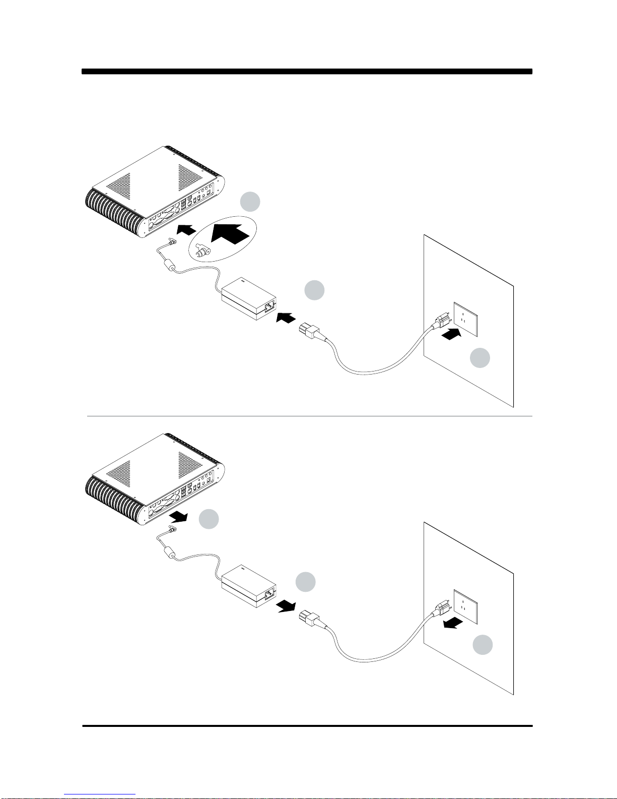
1. Before installing the power supply with this motherboard, please attach the 12V/DC
( 4 pin connector )of the adapter to motherboard first.
After that, plug the adapter power to AC outlet.
Always normally shut down the computer before you move the system unit or remove
the power supply from the motherboard.
Please unplug the 12V/DC ( 4 pin connector ) of the adapter from motherboard first.
Then unplug the adapter from the AC outlet.
Please refer to procedure from the photo 1
2. There will be high possibility to burn out the CPU if you change/ modify any parts of the
CPU cooler.
3. Please wear wrist strap and attach it to a metal part of the system unit before handling a
component.
You can also touch an object that is of ground connection or with metal surface if you don't
have wrist strap.
4. Please be careful when you handle this product. Pay attention to & don't touch the
sharp-pointed components at the bottom PCB .
5. Please pay attention to this: Remove or change any components form the motherboard
will VOID the warranty of the motherboard you purchased .
6. Before you install/remove any components or make any jumper setting on the motherboard,
please make sure to disconnect the power first.
( Please follow the instructions as of this guide )
7. Please only use single sided Mini PCI card, do not use the double sided Mini PCI card
which is not suitable.
8. This does not support 16 bit mini PCI card
9. Please follow this instruction carefully when using the "POWERON after PWR-Fair" function.
When the DC power adaptor runs out of power, unplug it from the DC current;
when power returns plug it back in only after 5 seconds. If there is a power outage,
unplug it from the AC current, when power returns plug it back in only after 30 seconds.
Otherwise it will cause system locking or serious damage.
Remark 1:
Always insert/unplug the 12V/DC ( 4 pin connector ) horizontally & directly from the
motherboard.
DO NOT twist the 12V/DC ( 4 pin connector ) gently, it is designed to fit snugly .
Moreover, erratic pull / push testing with the DC Jack might cause the unpredictable
damage to the component & system unit.
*
Page 8
3
Photo 1
2
1
3
1
2
3
Insert
Unplug
Page 9

4
The MI945A is an All-In-One Multimedia system control Board. The board's design combines
all necessary input and output effects interfaces, which makes itself an ideal all-in-one control
board for demanding multimedia applications. MI945A is the perfect platform for a whole
range of small form factor, low-power multimedia devices.
The MI945A’s Intel 945GME chipset features excellent flexibility for developers of embedded
applications by offering improved graphics and increased I/O bandwidth, as well as remote
asset management capabilities and improved storage speed and reliability.
It supports improved hardware motion compensation for MPEG2, all format decoder
(18 ATSC formats) supported. Dynamic Bob and Weave support video streams, Software DVD
at 60 Fields/second and 30 frames/ second full screen. MI945A on Board total has several
video outputs for different type of displays, including VGA, DVI, LVDS and TV-Out. Touch
screen controller and one video input are integrated on board to fulfill more applications’ need.
MI945A is supported with one 10/100/1000 Ethernet for seamless broadband connectivity,
with Wake On LAN function and the PXE function in BIOS for Realtek LAN chip only.
Except CompactFlash, MI945A can integrate with various type of PCI Card / Mini PCI Card.
In addition, with the 8 hi-speed USB version 2.0 enhanced host controller interface, the
MI945A ensures the high performance level and also the powerful and flexible expansion.
On board 2 x RS232 ports are reserved for connecting additional devices.
With Ultra DMA-100/66 access of mode 4 to IDE drive interface architecture, the IDE
supports maximum 100MB/sec in data transfer rating.
The MI945A All-In-One motherboard supports two DDR2 SODIMM up to 4GB. Compact Flash
reader supports IDE/ATA interface. A single Flash chip holds the system BIOS, and you can
change the Flash BIOS by the Utility Update.
The MI945A/ All-In-One motherboard is fully compatible with industry standards, plus
technical enhancements, and thousands of software applications developed for IBM PC/AT
compatible computers. The control logic provides high-speed performance for the most
advanced multi user and multitasking applications available today.
Chapter-1
General lnformation
Page 10

5
1. Intel Core 2 Duo / Core Duo CPU ( FSB 533/667 Mhz )
2. Intel 945GME Chipset on board, Graphic Chip Integrated
3. Support DDR2 SODIMM up to 4GB
4. Support 2 x 10 / 100 / 1000M LAN on Board ( Realtek LAN Chip ).
Support PXE / RPL Function (for Realtek LAN only)
5. Support Intel Gen 3.5 Integrated Graphics Engine
6. 18/36 bits LVDS Interface on Board. Support up to UXGA Resolution
7. Support touch screen on board (option)
8. Support TV-OUT and video-in
9. Support 1 x 40 Pins IDE and 1 x Compact Flash Card Socket on Board
10. Support 2 x SATA.
11. Support PCI gold finger on board, Mini PCI Socket on board,
and PCIe mini card for PCIe and USB interface (Note: -5V, -12V no support)
12. External +12V Power Supply
13. Compact PCB Dimension: 200 x 150 mm
1-1 Major Feature
Page 11

6
1. CPU : Intel Core 2 Duo / Core Duo CPU ( FSB 533/667 Mhz )
2. Chipset : Intel 945GME and Intel ICH7M (82801GBM)
3. Memory : two DDR2 SODIMM up to 4GB
4. VGA : Internal Graphics Memory supports DVMT 3.0
5. I/O Chip : ITE IT8712F IO
6. SATA : Two SATA ports with independent DMA operation supported on ports 0 and 2
7. Video-in : 1 port with Conexant Fusion CX23885 video codec
8. IDE : Ultra ATA 100/66/33, BMIDE and PIO mode
9. LAN : 2 x Realtek RLT8111C 10/100T/Giga, PCIe interface
10. Storage Device : 1 x 50 pins Compact Flash Socket
1 x 40 pins IDE
11. Serial Port : 2 x RS232
12. USB : 8 x USB 2.0
13. Keyboard & Mouse : PS/2 10pins Header
14. Sound : HD audio specification 1.0, 2 channel sound
15. LVDS : Support 18bits/36bits LVDS interface resolution up to 1600x1200
16. TV-Out : NTSC/PAL, HDTV support
17. WDT/DIO : Hardware watch dog timer support, 0~255 sec programmable. 8xDI/8x DO
18. Touch screen (option): C8051F321 USB interface touch screen controller,
support 4-, 5-, 8- wire Analog resistive touch screen
19. Expand interface : 1 x Mini PCI socket for PCI Rev. 2.2 interface,
1 x PCI gold finger for PCI Rev. 2.2 interface,
1 x PCIe Mini card for PCIe x1 and USB interface
20. BIOS : Award BIOS version V6.1
21. Dimension : 200 x 150 mm
22. Power : DC 12V-In (12V +-5%)
23. Power Consumption : Please refer to page 91
1-2 Specification
Page 12
7
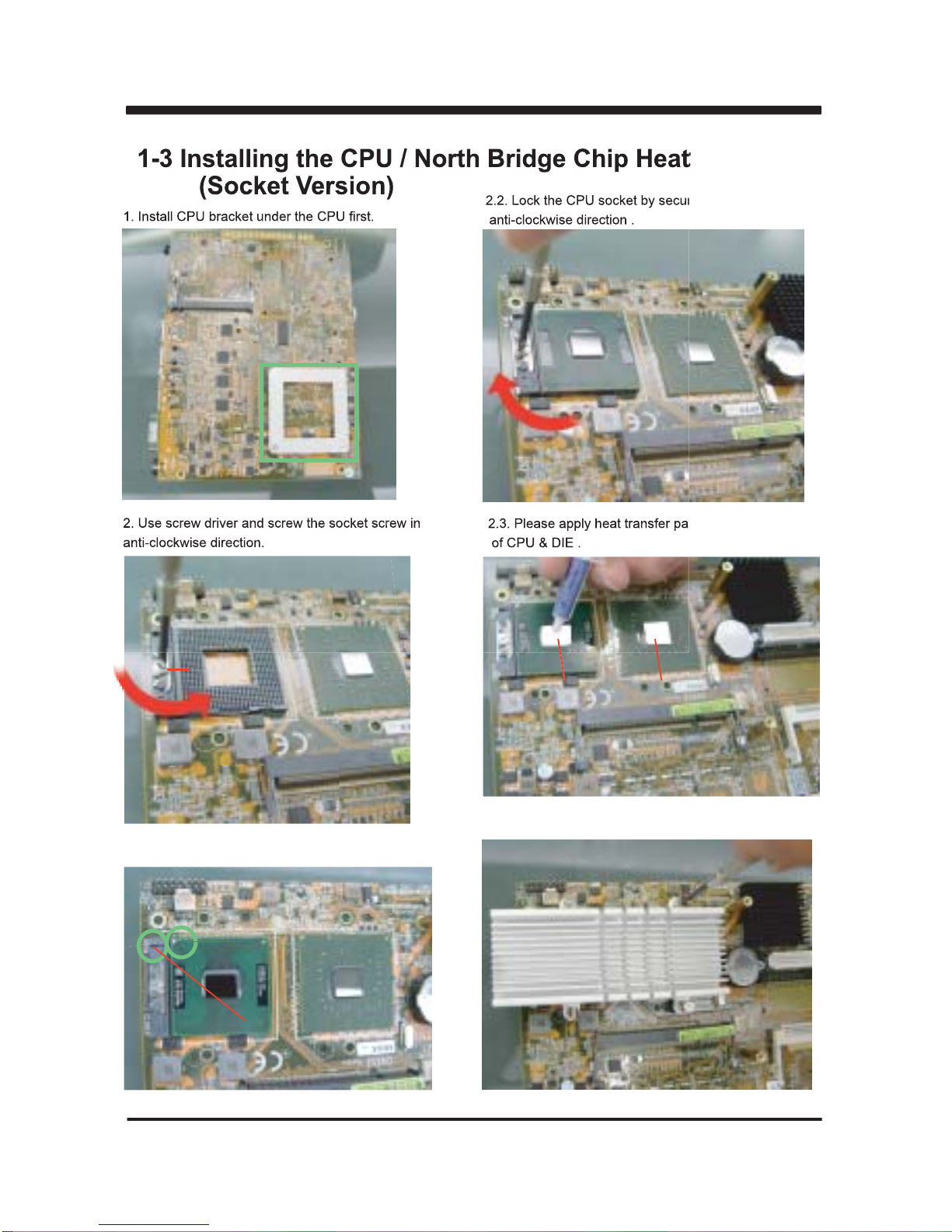
1-3 Installing the CPU / North Bridge Chip Heatsink.
(Socket Version)
2. Use screw driver and screw the socket screw in
anti-clockwise direction.
2.1. Locate Pin1 in the socket, look for a golden narrow .
Golden arrow
Socket Pin1
2.2. Lock the CPU socket by securing the screw in an
anti-clockwise direction .
2.3. Please apply heat transfer paste on the center
of CPU & DIE .
Heat transfer paste
1. Install CPU bracket under the CPU first.
Socket screw
Socket screw
3. Secure the 4 screws by using slotted screwdriver.
Page 13
8
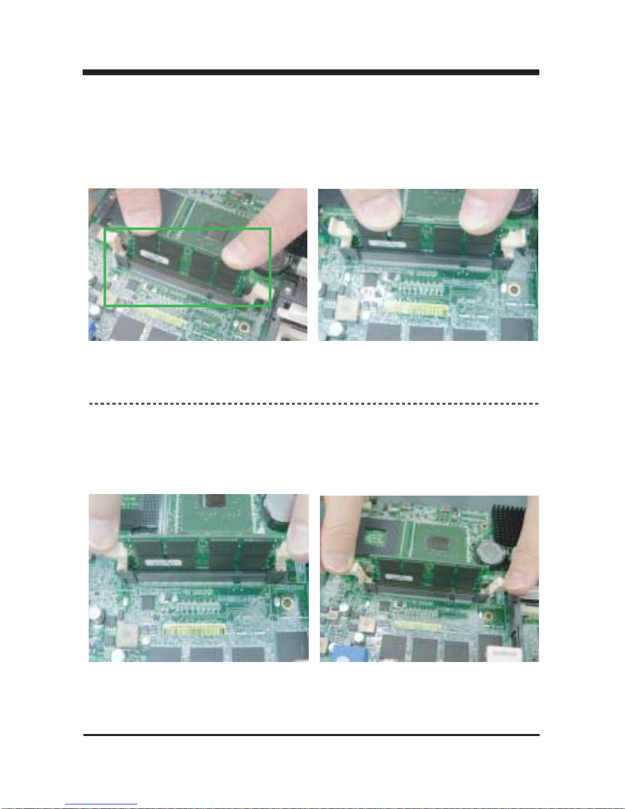
1-4 Vertical SODIMM assembly guide
1.
Install the memory into SODIMM.
2. Press down firmly to ensure the memory
is locked.
1. Pull open both sides of the memory slot. 2. Take out the memory.
Uninstall
Page 14
9
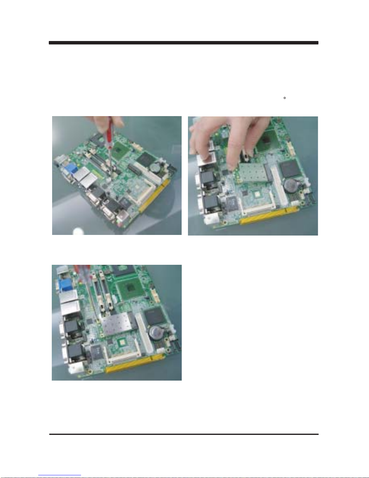
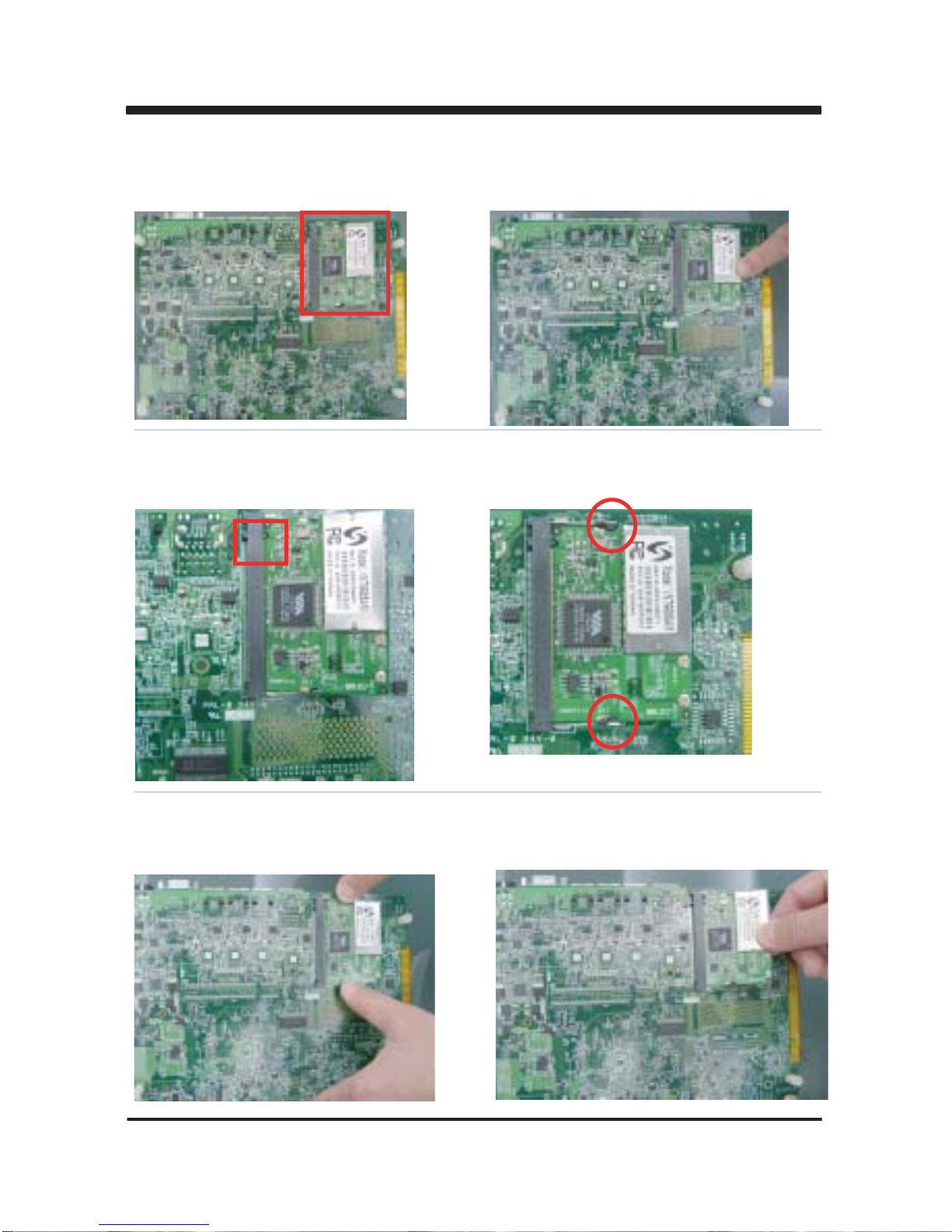
1-5 Directions for installing the Mini Card
1.
Unscrew the screw on the board
3. Gently push down the Mini Card and screw the screw back.
2. Plug in the Mini Card in a 45 angle
Page 15
10
1-6 Installing the Mini PCI card
1.Align the Mini PCI card with the connector at
a 45 degree angle.
2. Press the Mini PCI into the connector until you hear
a click.
Notices:
1.The connectors are designed to ensure the
correct insertion. If you feel resistance, check the
connectors & golden finger direction, and realign the card.
2. Make sure the retaining clips (on two sides of the slot)
lock onto the notches of the card firmly
1-6-1.1 Removing the Mini PCI card
1. Release the Mini PCI card by pulling outward
the two retaining clips and the card pops up slightly.
2. Lift the mini PCI card out of its connector carefully.
Page 16
11
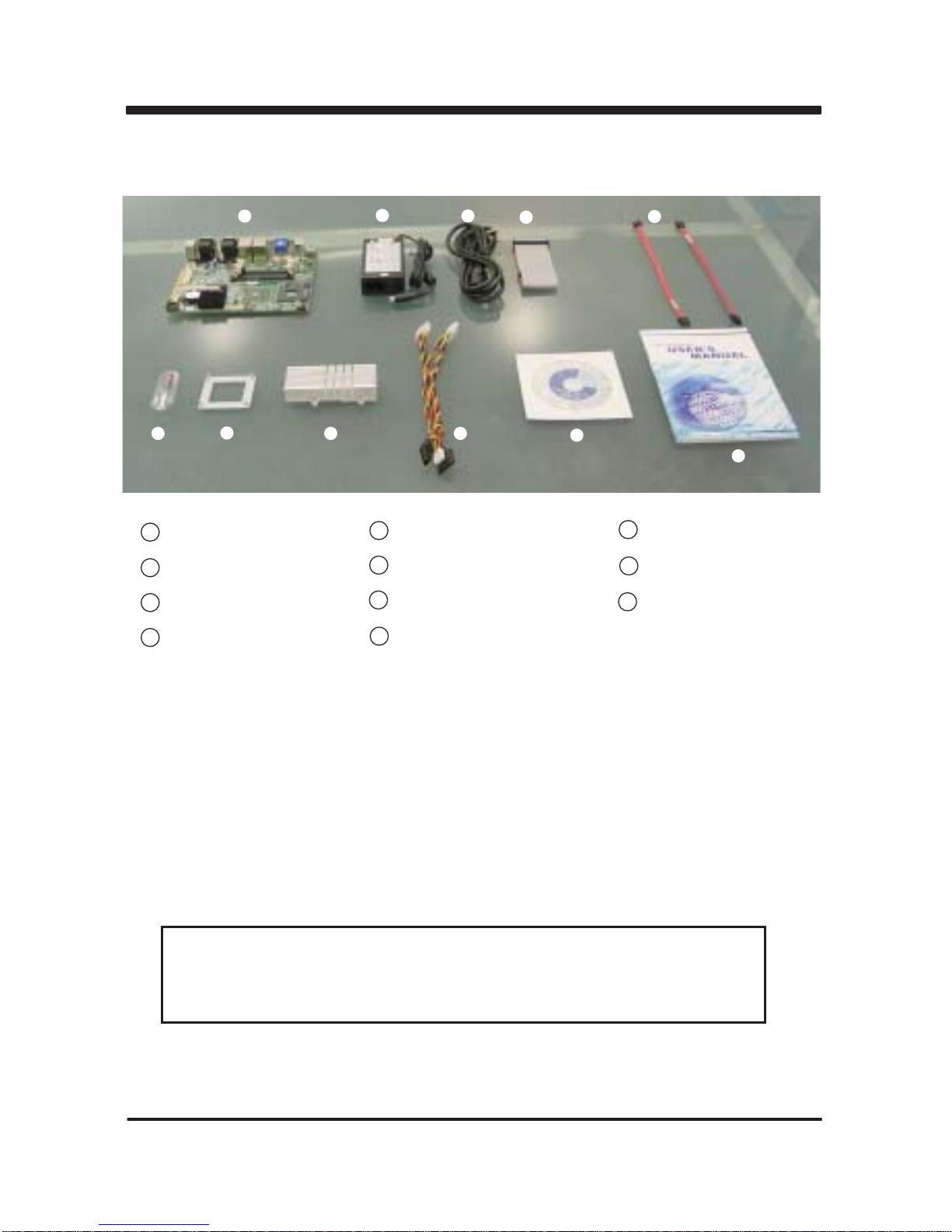
1-7 Packing List
Please contact with your dealer if any of these items is missing or damaged
on delivery. And please keep all parts of the delivery package with packing
materials in case if you need to deliver or store the product in the future.
*The packing list above is for the users who purchase single motherboard. The users
who purchase the board with chassis may refer to the packing list in the Assembly Guide.
1 MotherBoard
2 DC 12V Power Adapter(4P)
3 Power cord
4 ATA 66 HDD Cable(40P)
1
2
3
4
5
6
7
8
9
10
11
5 SATA HDD Cable(7P)
6 Haet Transfer Paste
7 CPU Heatsink Under Bracket
8 CPU+NB Heatsink
9 Power Cable
10 Utility CD Disk
11 User’s Manual
Page 17

12
Hardware Installation
This chapter provides the information how to install the hardware of MI945A.
Please follow section 1-6, 2-1 and 2-2 to check the delivery package and unpack
carefully. Please follow the jumper setting procedure.
Chapter-2
2-1 Unpacking Precaution
The MI945A board has been well packed with an anti-static bag to protect its
sensitive components and circuitry from damage due to static electric discharge.
You should follow these
steps to protect the board from the static electric
discharge whenever you handle the board:
1. Ground yourself by a grounded wrist strap at all times when you
handle the MI945A.
Well secure the ALLIGATOR clip of the strap to the end of the shielded wire lead from
a grounded object. Please put on and connect the strap before handling the
MI945A for harmlessly discharge any static electricity through the strap.
2. Please use anti-static pad to put any components, parts, or tools on the pad whenever
you work on them outside the computer. You may also use the anti-static bag instead of
the pad. Please ask your local supplier for necessary parts on anti-static requirement.
3. Do not plug any connector or set any jumper when the power is on.
1. Do not touch the board or any other sensitive components without all necessary
anti-static protection.
2. Please pay attention to the voltage limitation of DC-IN12 V 5 %.
Overuse of DC-IN voltage limitation or change to another power adapter
( not provided with this system ) will VOID warranty.
NOTE!
+
-
Page 18

13
2-2 Unpacking checkup
First of all, please follow all necessary steps of section 2-1 to protect MI945A
from electricity discharge. With reference to section 1-6, please check the delivery package
again with following steps:
1. Unpack the MI945A board and keep all packing material, manual
and driver disc etc, do not dispose !
2. Is there any components lose or drops from the board? DO NOT CONTINUE
TO INSTALL THIS BOARD! CONTACT THE DEALER YOU PURCHASED THIS
BOARD FROM, IMMEDIATELY.
3. Is there any visible damage on the board? DO NOT CONTINUE TO INSTALL
THIS BOARD!CONTACT THE DEALER YOU PURCHASED THIS
BOARD FROM, IMMEDIATELY.
4. Check your optional parts (i.e. DDR, CF etc.), all necessary jumpers
setting to jumper pin-set, and CMOS setup correctly.
Please also refer to all information of jumper settings in this manual.
5. Check your external devices (i.e. Add-On-Card, Driver Type etc.)
for complete add-in or connection and CMOS setup correctly.
Please also refer to all information of connector connection in this manual.
6. Please keep all necessary manual and driver disc in a good condition for future
re-installation if you change your Operating System.
Page 19
14
2-3 Dimension 200 x150m
32.50
132.65
191.87
200.00
156.31
175.49
53.44
9.50
16.60
1.20
25.48
3.70
6.28
84.48
105.72
24.00
14.38
65.38
79.00
150.00
6.20
1.85
2.80
19.10
22.35
19.10
rj45 rj45
93.090
6.21
6.21
68.36
68.36
MI945A-M0.2
MI945A-M0.2
2008,09,08
2008,09,08
Page 20
CN4
CN16
JV1
CN22
JV2
CN21
JC8
JKM1
CN15
CN14
CN5
CN2
CN6
CN11
CN10
CN8
JSV1
CN20
CN7
CN1
CN13
CN3
JF1
CN24
CN23
CN25
JCF1
CN27
CN26
CN30
CN32
CN29
JCF2
CN31
SATA1
SATA2
JUV1
CN28
CN33
CN35
CN42
CN41
JF2
JAT1
CN43
SODIM1
SODIM2
CN37
CN38
JV4
JT1
JB1
CN40
JV3
CN39
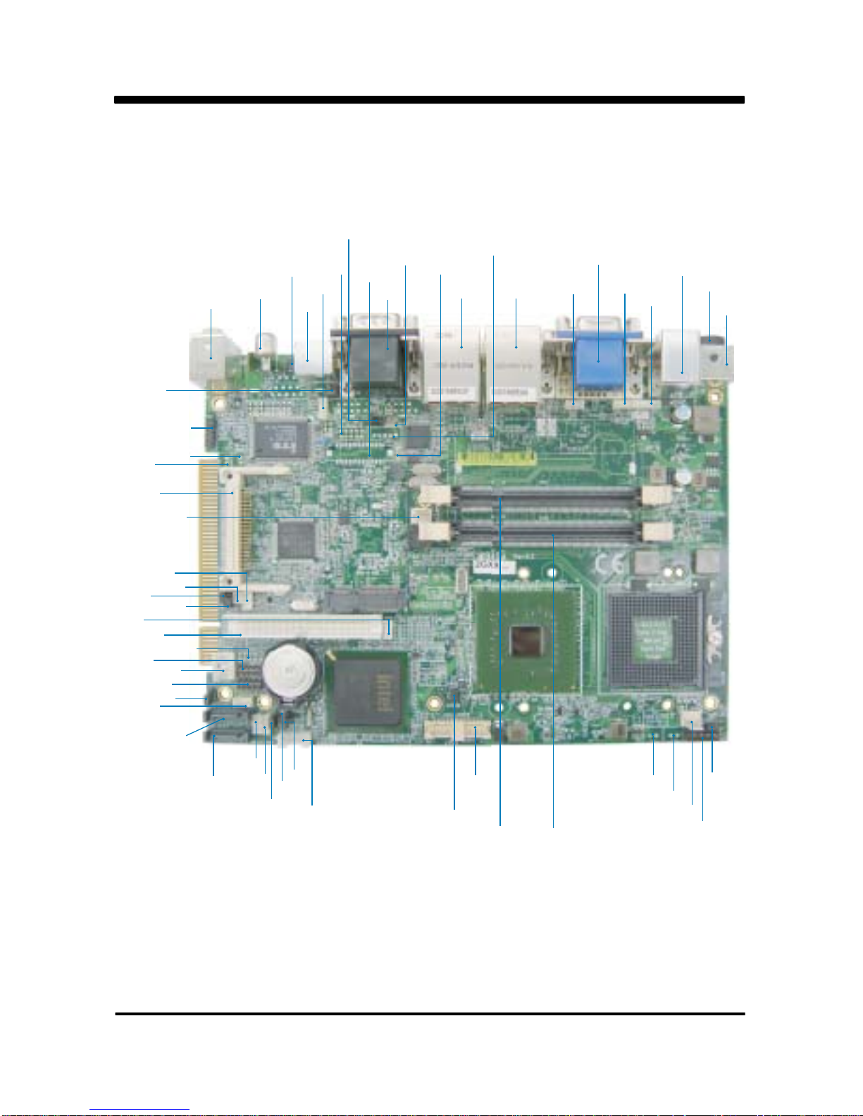
Layout2-4
15
JC1
CN19
Page 21
CN4
CN16
JV1
CN22
JV2
CN21
JC8
JKM1
CN15
CN14
CN5
CN2
CN6
CN11CN10
CN1
JSV1
CN20
CN7
CN13
CN3
JF1
CN24
CN23
CN25
JCF1
CN27
CN26
CN30
CN32
CN29
JCF2
CN31
SATA1
SATA2
JUV1
CN28
CN33
CN35
CN42
CN41
JF2
JAT1
CN43
SODIM1
SODIM2
CN37
CN38
JV4
JT1
JB1
CN40
JV3
CN39
Diagram2-5
16
JC1
CN19
Page 22
17
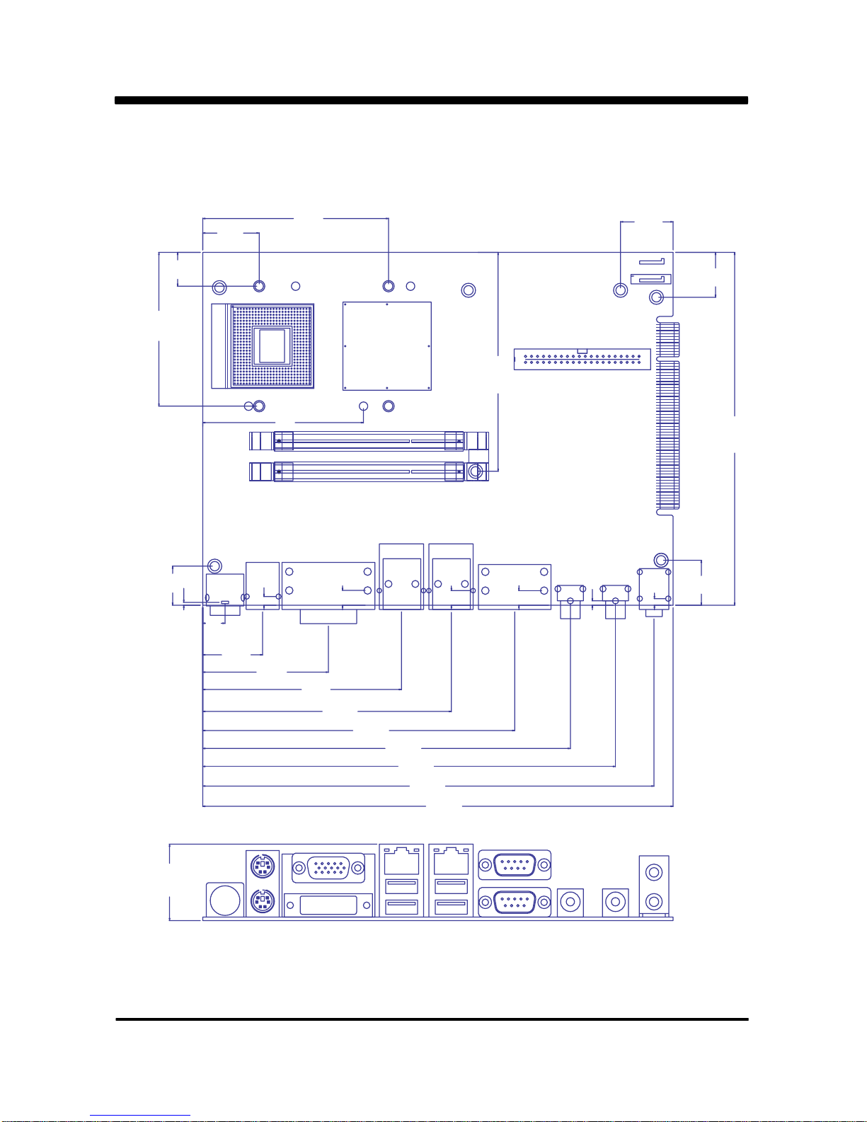
2-5-1 Bottom Side Diagram
DC12VIN
PS/2 Keyboard
DVI
COM2
S-Video Out
Mic-in
Line-Out
VIDEO-IN
COM1
LAN1LAN2
VGA
PS/2 Mouse
USB USB
Back Panel
MPCI: Mini PCI Socket
Page 23
18
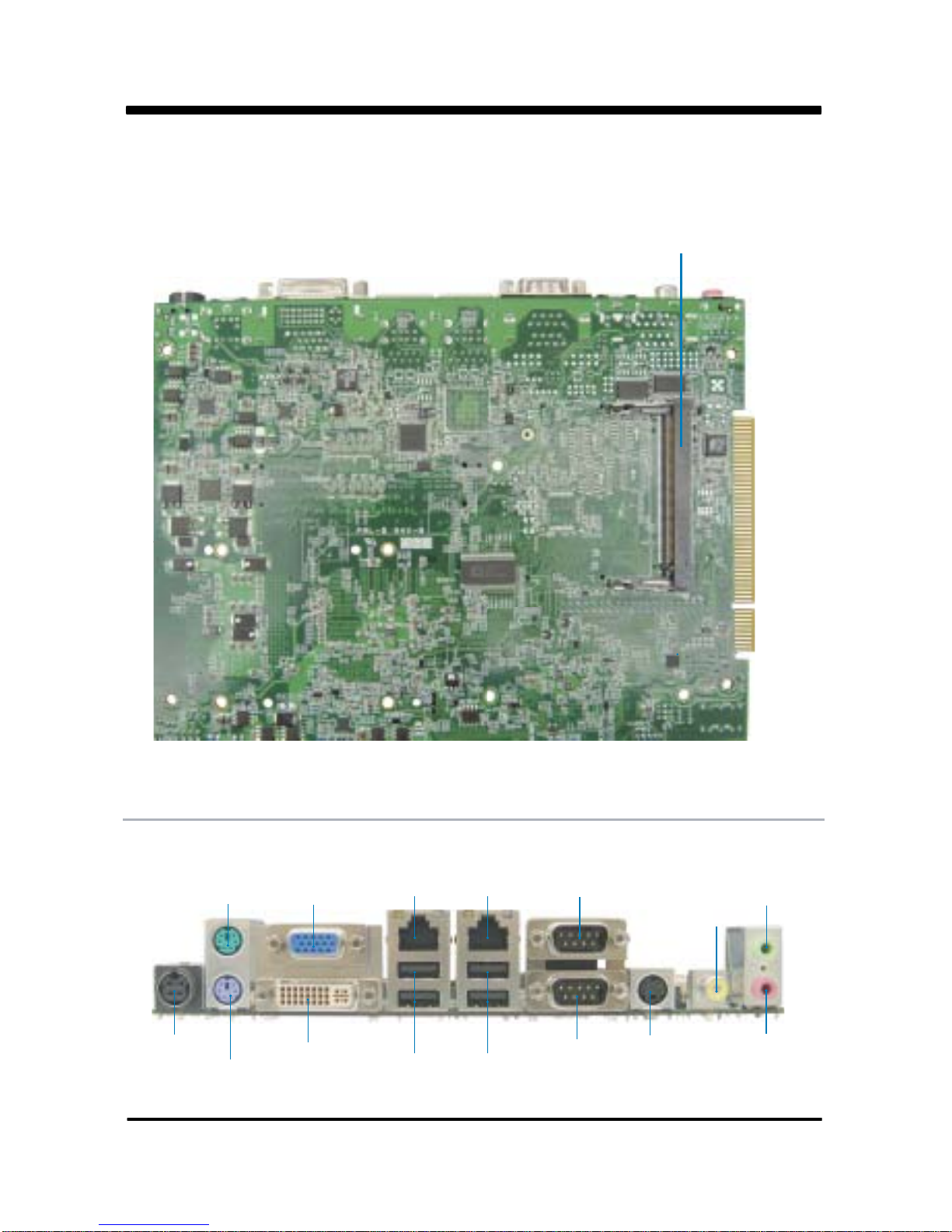
2-6 Install Memory
This motherboard provides one 200-pin Small Outline Dual In-line Memory Module
(SODIMM) socket for memory expansion available from minimum memory size of 256MB
to maximum memory size of 4GB DDR2 RAM.
DDR2 clock supports: DDRII533, DDRII667
Valid Memory Configurations
DS: Double Sided DIMM
SS: Single Sided DIMM
The detected memory size is less than actual installed memory size since
some memory has been allocated for system use.
That’s how PC works with system memory.
NOTE!
System Accept or Not
DIMM1
Total Memory
Min. ~ Max.
DS/SS Accept
256MB~4GB
Page 24

19
NOTE!
When you install DIMM module fully into the DIMM socket, the eject tab should be
locked into the DIMM module very firmly and fit into its indention on both sides.
WARNING!
Once you hear " Beep Beep Beep" sounds after turning on the power ,
please check if the DRAM is installed properly or not.
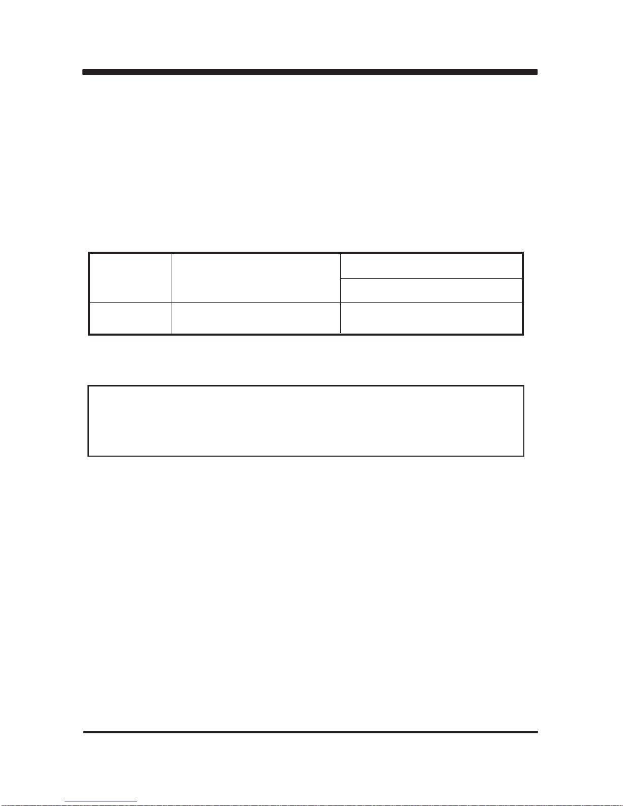
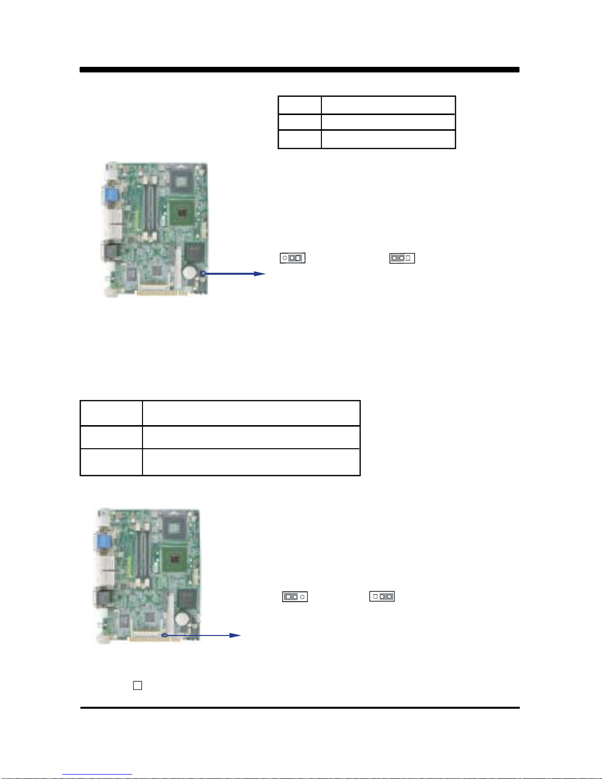
2-7 List of Jumpers
JB1 : CMOS DATA SET
JCF1 : CF card Power +5V/+3.3V select
JCF2 : CF card master and slave select
JT1 : USB / COM Touch control select
JAT1 : AT/ATX power select
JC8 : COM1 power select
JC1 : COM2 power select
JV2 : LVDS1 power select (2 )
JV1 : Inverter power select (2 )
JV3 : LVDS Power select (1 )
JV4 : Inverter Power select (1 )
JUV1 : USB Port 4 Power select
JSV1: S Video / HDTV select
nd
nd
nd
nd
Please refer to page8 for installation of memory module.
Page 25
20
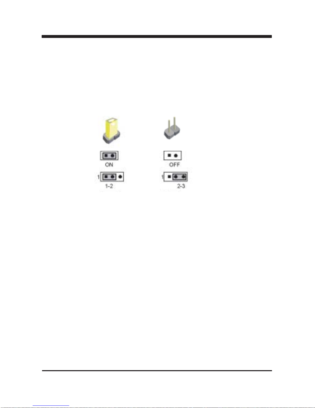
A jumper is ON as a closed circuit with a plastic cap covering two pins. A jumper is OFF
as an open circuit without the plastic cap. Some jumpers have three pins, labeled 1, 2,
and 3. You could connect either pin 1 and 2 or 2 and 3.
The below figure 2.2 shows the examples of different jumper settings in this manual.
2-8 Jumper Setting Description
Figure 2.2
2-9 CMOS Data Set
A battery must be used to retain the motherboard configuration in CMOS RAM.
Close pin 1and pin 2 of JB1 to store the CMOS data.
To clear the CMOS, follow the procedures below:
1. Turn off the system and unplug the AC power
2. Remove DC 12V power cable from DC 12V power connector
3. Locate JB1 and close pin 2-3 for a few seconds
4. Return to its normal setting by shorting pin 1-2
5. Connect DC 12V power cable back to DC 12V power connector
All jumpers already have its default setting with the plastic cap inserted as ON,
or without the plastic cap as OFF. The default setting may be referred in this
manual with a " " symbol .
*
Page 26
21
Note: Do not clear CMOS unless
1. Troubleshooting
2. Forget password
3. You fail over-clocking system
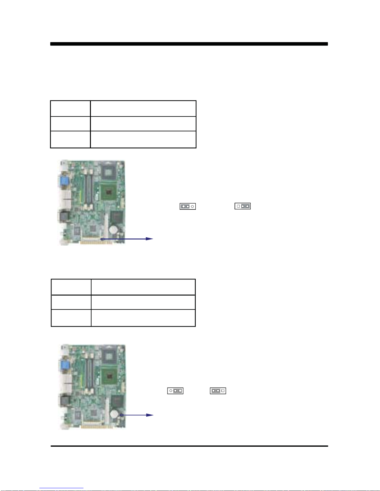
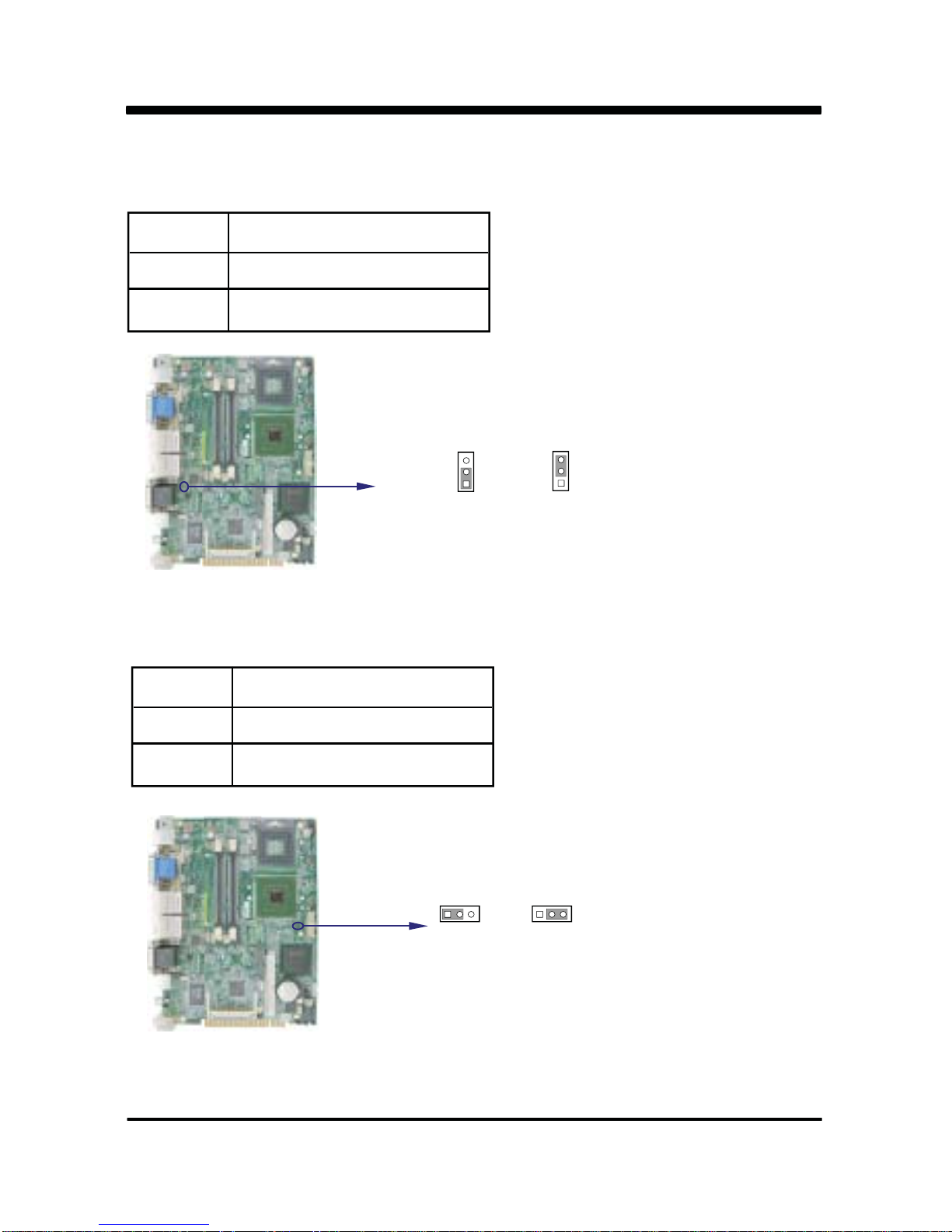
2-10 JCF1 CF Card Power Voltage select
JCF1 Description
*1-2 *For CF CARD power voltage select +5V
2-3 For CF CARD power voltage select +3.3V
JB1 Description
*1-2 *Normal Set
2-3 CMOS Data clear
*Normal
JB1
JCF1
If you use CF card and HDD together, we suggest you
use the jumper setup for +5V.
2
Clear Setting
3.3V
12
3
12
3
+5V*
* We use to refer to as pin1
13213
Page 27
22
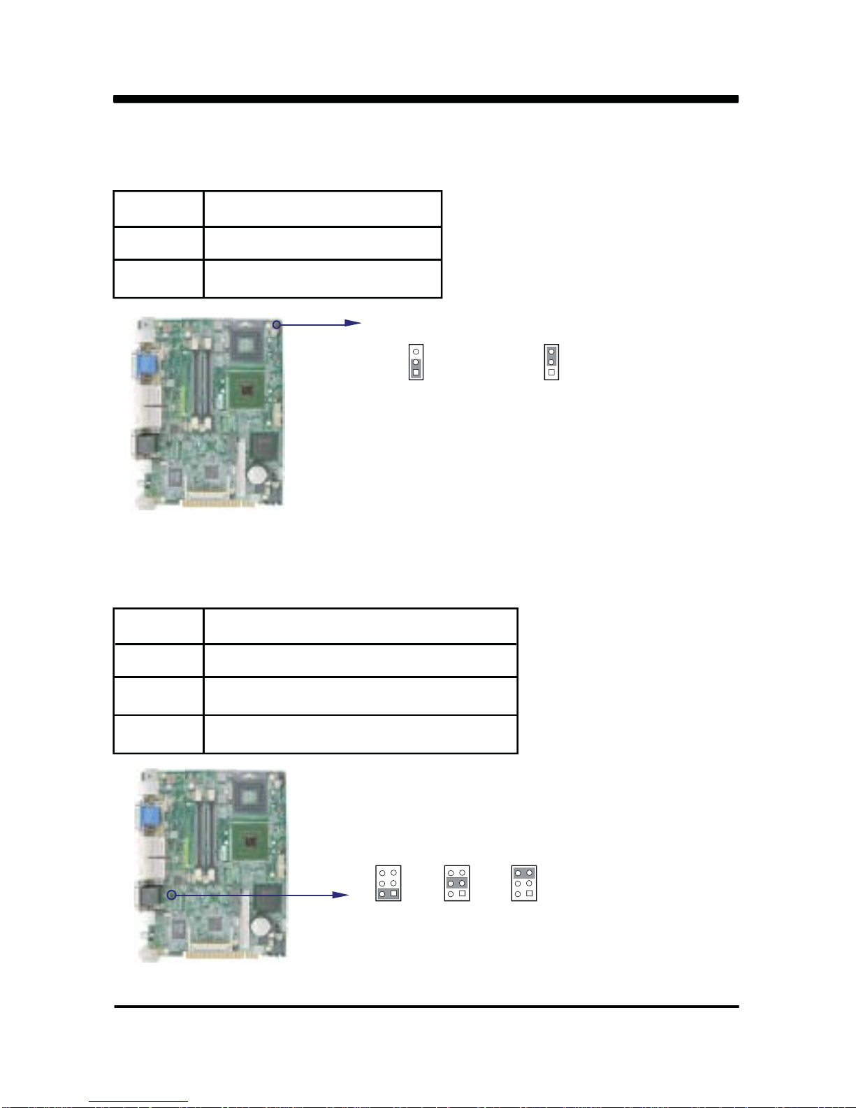
2-11 JCF2 CF Card Master and Slave selection
JCF2 Description
*1-2 For CF CARD Master
2-3 For CF CARD Slave
If you use CF card and HDD together, please set CF as Master and HDD as Slave.
JCF2
Master
*
Slave
COM6USB6
12
3
12
3
2-12 JT1: USB / COM Touch control select
JT1 Description
1-2 Share to USB6 ports
2-3 Share to COM6 ports
JT1
12
3
12
3
Page 28
23
2-13 JAT1 AT and ATX selection
JAT1 Description
*1-2 *ATX Power mode
2-3 AT Power mode
JA T1
A TX Power
*
AT Power
1
2
3
1
2
3
2-14 JC8 : COM1 power select
JC8 Description
1-2 use RI signal or did not power.(Default)*
3-4 For COM1 power voltage select +5V
5-6 For COM1 power voltage select +12V
JC8
RI signal*
1
2
34
65
1
2
34
65
1
2
34
65
+5V +12V
Page 29
24
2-15 JC1: COM2 power voltage select
JC1 Description
1-2 use RI signal or did not power.(Default)*
3-4 For COM2 power voltage select +5V
5-6 For COM2 power voltage select +12V
JC1
123465 123465 123465
+5V +12VRI signal*
2-16 JV2 : LVDS panel power select (2 )
JV2 Description
1-2 +5V
2-3 +3.3V
JV2
+5V
12
3
12
3
+3.3V
nd
Page 30
25
2-17 JV1 : Inverter power select (2 )
JV1 Description
1-2 +12V
2-3 +5V
JV1
+5V
1
2
3
1
2
3
+12V
nd
2-18 JV3 : LVDS Panel power select (1 )
JV3 Description
1-2 +5V
2-3 +3.3V
JV3
+5V
12
3
12
3
+3.3V
nd
Page 31

26
JV4
+5V
12
3
+12V
2-19 JV4 : Inverter power select (1 )
JV4 Description
1-2 +12V
2-3 +5V
nd
12
3
2-20 JUV1 : USB Port 4 power select
JUV1 Description
1-2 +5V
2-3 +3.3V
JUV1
+5V
321 321
+3.3V
Page 32

27
JSV1
S Video
1
2
HDTV
2-21 JSV1: S Video / HDTV select
JSV1 Description
OPEN S Video
Short HDTV
1
2
Page 33

28
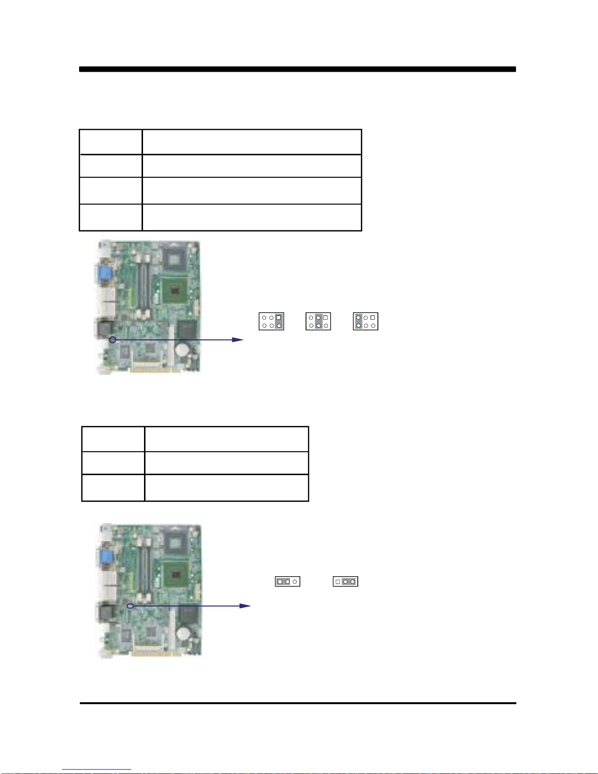
3-1 List of Connectors
This chapter provides all necessary information of the peripheral's connections,
switches and indicators. Always power off the board before you install the peripherals.
Chapter-3
Connection
CN2: DC 12V-IN DIN external Connector (4pin mini din connector)
CN6: DC 12V-IN Internal Connector (4pin connector) (Option)
CN5: PS2 Keyboard / Mouse connector
JKM1: PS2 Keyboard /Mouse Internal Connector 1x6 pin (1.25mm)Wafer
CN4: DVI-D / VGA DB15P connector
CN11: USB port 2/3 and LAN2 RJ45 Connector
CN10: USB port 0/1 and LAN1 RJ45 Connector
CN13: COM1(up side)/COM2(down side) DB9P connector
CN16: COM2 for Touch pad connector
CN8: RCA jack Video out connector (share to CN1)
CN1: S-Video mini din Video out connector
CN7: RCA Jack Video in connector from CX23885 VIN1.
CN3: Mic-in (down side) / Line out (up side) phone jack
CN19: 7.1 Sound out 2x6pin(2.0mm) Header
CN23: Amplifier Line-out Right channel connector (option)
CN24: Amplifier Line-out Left channel connector (option)
CN28: IDE1 40 pin (2.54mm) Connector
CN25: CF 50 pin socket
SATA1: S-ATA IDE 7 pin Wafer
SATA2: S-ATA IDE 7 pin Wafer
CN39: LVDS 18/36Bits 2x15 pin (1.25mm) connector
CN40: LVDS inverter power connector 5 pin (2.0mm) Wafer
CN30: Touch screen device 2x5 pin (2.0mm) Header (option)
CN32: DIO 0--3 connector 2x5pin (2.0mm) Header
CN33: DIO 4--7 connector 2x5pin (2.0mm) Header
Page 34

29
List of Connectors
CN35: USB port4 4 pin (1.25mm) Wafer
CN37: USB port5 4 pin (1.25mm) Wafer
CN38: USB port6 4 pin (1.25mm) Wafer (share with Touch)
CN29: USB port7 4 pin (1.25mm) Wafer
CN27: Conexant CX23885 port1/2 Audio in
CN26: Conexant CX23885 VIN2 Vido in
MPCI1: Mini PCI socket
SK1: PCIe Mini card socket
CN31: DC +5/+12V output connector (2.5mm) Wafer
JF2: CPU FAN connector 1x3 pin (2.54mm) Wafer
JF1: System FAN connector 1x3 pin (2.54mm) Wafer
CN41: FP ports 2x5pin (2.54mm) Header
CN22: LVDS(2nd) 24/48Bits 2x15 pin (1.25mm) connector (option)
CN21: LVDS(2nd) inverter power connector 5 pin (2.0mm) Wafer (option)
CN20: VGA(2nd) 2x5pin Header (option)
SODIMM 1/2 :DDRII RAM SOCKET
CN14: VGA RGB Signal(1nd) 4pin (1.25mm) wafer
CN15: VGA Controller Signal (1nd) 5pin (1.25mm) wafer
Page 35

30
3-2 FAN Connector
MI945A provides one CPU fan connector and one system fan connector.
JF2: CPU FAN connector
JF1: System FAN connector
PIN NO. Description
1 FAN GND PIN
2 +12V*
3 FAN speed Sensor
pin1
JF2
pin1
JF1
*Note : DC in +12V by switch to FAN power +12V,
so DC in need stable +12V input
3-3 Serial ATA
PIN NO. Description
1 GND
2 DA TA TX+
. SAT A1 / SATA2 : S-ATA IDE 7pin Wafer
3 DA TA TX-
4 GND
5 DA TA RX6 DA TA RX+
7 GND
SATA1
SATA2
Page 36

31
3-4 IDE Connectors
PIN NO. Description PIN NO. Description
1 RESET# 2 GND
3 DATA7 4 DATA8
5 DATA6 6 DATA9
7 DATA5 8 DATA10
9 DATA4 10 DATA11
11 DATA3 12 DATA12
13 DATA2 14 DATA13
15 DATA1 16 DATA14
17 DATA0 18 DATA15
19
21
23
25
27
29
31
33 SA 1 34 ATA 33/66/100
CABLE SELECT
GND
DREQ
IOW#
IOR#
IORDY
DACK#
IRQ15
20
22
24
26
28
30
32
+5V
GND
GND
GND
PULL DOWN
GND
NC
35
36
40
37
39
38
SA 0
SA 2
HD CS0#
HD LED
HD CS1#
GROUND
Note: Refer JCF1/JCF2 Jumper set (CF socket share to IDE)
Note!
PIN 20 connector +5V of IDE 1 could
provide the power of DOM.
CN28: IDE1 40 pin (2.54mm box Header) Connector
pin1
IDE1
CN28
(IDE1)
Page 37

32
CN25: CF Socket Connector (For True IDE Mode)
GND(-CD1)
DATA11
DATA12
DATA13
DATA14
DATA15
-CS1
GND(-VS1)
-IOR
-IOW
-WE(PH)
INTR
+5V or +3.3V
-CSEL
NC(-VS2)
RESET
IORDY
DMAREG(-INP ACK)
DMAACK[-REG(PH)]
-DASP
-PDIAG
DATA8
DATA9
DATA10
GND
26
27
28
29
30
31
32
33
34
35
36
37
38
39
40
41
42
43
44
45
46
47
48
49
50
1
2
3
4
5
6
7
8
9
10
11
12
13
14
15
16
17
18
19
20
21
22
23
24
25
GND
DA TA3
DA TA4
DA TA5
DA TA6
DA TA7
-CS0
GND(A10)
GND(-A TA_SEL)
GND(A9)
GND(A8)
GND(A7)
+5V or +3.3V
GND(A6)
GND (A5)
GND (A4)
GND (A3)
SDA2
SDA1
SDA0
DA TA0
DA TA1
DA TA2
NC(-IOCS16)
GND(-CD2)
PIN NO. DESCRIPTION PIN NO. DESCRIPTION
3-5 Compact - Flash Memory Socket
MI945A configures CompactFlash Storage Card in IDE mode.
It will use IDE channel when CompactFlash card is plugged in.
This socket supports CF Card Type I/II socket spec.
CF Socket 50pin----CN25
CN25
Page 38

33
3-6 VGA Connector
PIN NO. Description PIN NO. Description PIN NO. Description
1 RED 6 GND 11 NC
2 GREEN 7 GND 12 DDC DATA
3 BULE 8 GND 13 H-SYNC
4 NC 9 NC 14 V -SYNC
5 GND 10 GND 15 DDC CLOCK
. CN4: (Up side) VGA DB15 connector (D-SUB 15PIN)
CN4 VGA
PIN NO. Description PIN NO. Description
1 Data 2 - 9 Data 1 2 Data 2 +
3
4
5
6
7
8
. CN4 : DVI 12bit connector Down side (DB Connector)
NC NC
NC
NC
NC
10
11
GND
Data 1+
12
13
GND
I2C-CLK
I2C-DA TA
GND
GND
Description PIN NO.
14
15
16
+5V
DVI-DETECT
17
18
19
20
Data 0 Data 0 +
GND
21
22
NC
NC
23
24
CLK+
CLK-
3-7 DVI-D Connector
CN4 DVI
Page 39

PIN NO. Description
1 MS DATA
2 NC
3 GND
4 +5V
5 MS CLOCK
6 NC
34
3-8 Keyboard and Mouse Connector
. CN5: PS2 Keyboard down side (Din 6 pin jack)
PIN NO. Description
1 KB DA TA
2 MS DA TA
3 GND
4 +5V
5 KB CLOCK
6 MS CLOCK
. CN5: PS2 Mouse up side (Din 6 pin jack)
CN5
PS/2 Mouse
CN5
PS/2 Keyboard
PIN NO. Description
1 +5V
2 KB DA TA
3 KB CLOCK
4 GND
5 MS DA TA
6 MS CLOCK
. JKM1: 6 pin(1.25mm Wafer connector) Internal Keyboard / Mouse Connector
pin1
JKM1
Page 40

35
3-9 USB Port/ Header
. CN35 / CN37 / CN38 / CN29: USB port 4 / 5 / 6 / 7
4pin (1.25mm Wafer connector)
PIN NO. Description
1 +5V
2 USB DA TA 4 / 5 / 6 / 7-
3 USB DA TA 4 / 5 / 6 / 7+
4 GND
. CN11 / CN10(Down side): USB ports 0 / 1 / 2 / 3 Type A jack
pin1
CN29
pin1
CN37
pin1
CN35
pin1
CN38
Note: If use CN35 will need check JUV1 USB Voltage setting.
PIN NO. Description
1 +5V
2 USB DA TA 0 / 1 / 2 / 3 / 4 -
3 USB DA TA 0 / 1 / 2 / 3 / 4 +
4 GND
CN11 CN10
Page 41

36
3-10 LAN Port
The Fast Ethernet controller provides 32-bit performance, PCIe bus master capability, and full
compliance with IEEE 802.3 10/100/1000Based-T specification.
For 10/100/1000Base-T operation, please connect the network connection by plugging one end of
the cable into the RJ-45 jack of the CN10/CN11 Connector.
Besides 10/100/1000 Base-T, MI945A can provide Intel Giga LAN solution through CN10/CN11
once equipped with Intel 82573L chipset.
. CN10/CN11 (Up side) : RJ45 LAN Giga/100Mb Jack
PIN NO. Description PIN NO. Description
1 TD0-/TX+ 5 TD2-/NC
2 TD0+/TX- 6 TD2+/RX 3 TD1-/RX+ 7 TD3-/NC
4 TD1+/NC 8 TD3+/NC
RJ45 CN10
RJ45 CN11
LAN LED
Speed
Indicate
10 Mbps 100
Mbps 1000 Mbps
Back Side
LAN light
Fornt Side
Link Led
Orange Orange Orange Orange Orange Orange OrangeRedGreen
ACT Led ACT Led ACT Led ACT Led ACT Led ACT LedLink Led Link Led
Back Side Fornt Side Back Side Fornt Side
Intel 82573L
LAN LED
Speed
Indicate
10 Mbps 100
Mbps 1000 Mbps
Back Side
LAN light
Fornt Side
Link Led
Orange Orange Orange OrangeRedGreen
ACT Led ACT Led ACT Led ACT Led ACT Led ACT LedLink Led Link Led
Back Side Fornt Side Back Side Fornt Side
Realtek RTL8111C
LAN LED
Page 42

37
3-11 COM Port Connector
PIN NO. Description PIN NO. Description
1 DCD 6 DSR
2 RXD 7 RTS
3 TXD 8 CTS
4 DTR 9 RI or VOL TAGE
5 GND
. CN13: COM1(up side) / COM2(down side) port Connector
Note: PIN9 VOL TAGE / RI select Jumper -->JC1/JC8
RS232 Mode COM port conector D-SUB 9PIN
CN13: COM1
CN13: COM2
pin1
CN16
. CN16 : 5pin (1.25mm Wafer connector)
PIN NO.
Description
12 3 4 5
+5V GND RTS TX RX
CN16: COM2 for Touch pad header All Signal are RS232 level ( COM2)
Page 43

38
3-12 Audio Port Connector
The MI945A has an on-board AC'97 3D sound interface. There are the connectors of
LINE OUT, MIC-IN and connectors.
The MIC-IN Jack and header are for audio sound input. The LINE-OUT
connector is a 4-pin Jack for audio sound output.
PIN NO. Description
1 GND
2 Line OUT-L
3 NC
4 NC
5 Line OUT_R
. CN3:Up side Line out
(3.5mm phone jack)
PIN NO. Description
1 GND
2 Mic IN-L
3 NC
4 NC
5 MIC-IN_R
. CN3: Down side Mic in
(3.5mm phone jack)
Mic-in CN3
Line-out CN3
. CN23 : 2.0mm Box Wafer (Option)
pin1
CN23
PIN NO. Description
1 Speaker Right output +
2 Speaker Right output -
. CN24 : 2.0mm Box Wafer(Option)
PIN NO. Description
1 Speaker Left output +
2 Speaker Left output -
CN23/CN24 : For internal stereo 6W class –D audio amplifier to 8Ω Speaker
Note : If phone jack plunge in CN3 of the signal will disabled CN23/CN24 Function.
CN24
pin1
Page 44

39
3-13 Video out Connector
. CN1 : S-VIDEO TV -out for Din 4pin Connector
PIN NO. Description
1 Composite-In
2 GND
PIN NO. Description
1 GND
2 CVBS / Pb
3 LUMA-out / Y
4 CHROMA-out / Pr
. CN8 : Composite TV -out for RCA Jack connector
CN1: S-Video out
Note: CN1 can support HDTV by external cable.
Note: CN1/CN8 : SVideo and RCA jack is share.
Page 45

40
pin1
CN26
CN27
pin1
3-14 Cx23885 Video in / Audio in
. CN7 : Composite in for RCA Jack connector
. CN27 : for Cx23885 Audio in (4pin 1.25 mm wafer) (TBD)
PIN NO. Description
1 Audio 1
2 GND
3 GND
4 Audio 2
CN7: Video in
PIN NO. Description
1 Composite-In
2 GND
Note: Video composite signal from CN7 will into Cx23885 chipset port 1
Note: Audio analog in signal from CN27 will
into Cx23885 chipset audio in port 1/2.
. CN26 : Composite in for (2pin 1.25mm wafer) (TBD)
PIN NO. Description
1 Composite-In
2 GND
Note: Video composite signal from CN26 will into Cx23885 chipset port 2
Page 46

PIN NO. Description PIN NO. Description
1 DI-4 2 DO-7
3 DI-5 4 DO-6
5 DI-6 6 DO-5
7 DI-7 8 DO-4
9 GND 10 +5V
Note : Please refer to page 42 for DIO/WDT sample code .
PIN NO. Description PIN NO. Description
1 DI-0 2 DO-3
3 DI-1 4 DO-2
5 DI-2 6 DO-1
7 DI-3 8 DO-0
9 GND 10 +5V
WDT/DIO Function port (2x5 2.0mm Header)
CN32 Digital Input / Output Connector
pin1
CN32
41
3-15 WDT/DIO Function port
CN33 Digital Input / Output Connector
3-15-1 For F75111N I2C watch dog timer device:
DIO function:
Logic 0 Level :+0.5V Max , Logic 1 Level : +4V Min
WatchDog function:
The system will be issued reset. When WDT is enable the hardware start down
counter to zero. The reset timer have 10~20% tolerance upon the Temperature.
-----------------------------------------------------------------Sample W75IO Demo Program
------------------------------------------------------------------
1. DI
2. DO
3. WatchDog
4. Exit
-----------------------------------------------------------------Please select demo function<1-4>?
1. DI: Input DI value (0~FF, DI bit 0~7 HI level)
2. DO: Input DO value (0~FF, DO bit 0~7 HI level)
3. WatchDog: Input WatchDog Value (0~256 sec)
4. Exit: Exit program
CN33
Page 47

42
3-16 I2C WDT/DIO W75IO.h Reference sample code:
Compile platform:TC30 & DOS 6.22
// Sample.cpp : Defines the entry point for the console application.
//
#include "stdafx.h"
#include "conio.h"
#include <string.h>
#include <stdlib.h>
#include <iostream>
#include "W75IO.h" /* include W75IO.h */
#define DEMO_DI 1
#define DEMO_DO 2
#define DEMO_WDT 3
#define DEMO_EXIT 4
/* demo function */
int menu();
BOOL W75IO_init();
void W75IO_DO();
void W75IO_DI();
void W75IO_WDT();
int stoi(char* str)
{
if (( strlen(str) < 0 ) || ( strlen(str) >= 3 ))
return -1;
int value = 0;
for (int i=0; i<strlen(str) ;i=i+1)
{
int result=0;
switch (str[i])
{
case '0':result=0;
break;
case '1':result=1;break;
case '2':result=2;break;
case '3':result=3;break;
case '4':result=4;break;
case '5':result=5;break;
case '6':result=5;break;
case '7':result=7;break;
case '8':result=8;break;
case '9':result=9;break;
case 'a':
case 'A':result=10;break;
case 'b':
case 'B':result=11;break;
case 'c':
case 'C':result=12;break;
case 'd':
case 'D':result=13;break;
case 'e':
case 'E':result=14;break;
case 'f':
case 'F':result=15;break;
Page 48

43
default:
result=-1;
break;
}
if (result == -1)
return -1;
if (strlen(str) == 1 )
value=value+result;
if (strlen(str) == 2 )
{
if ( i == 0 )
{
value=value+result*16;
}
if ( i == 1 )
{
value=value+result;
}
}
}
return value;
}
BOOL W75IO_init()
{
/* First step :to init W75IO.DLL */
if (InitializeW75IO())
{
/* init onboard W75IO chipset */
if (InitInternalW75IO())
return TRUE;
else
{
printf("ERROR:init Onboard W75IO chipset!!!!.\n");
return FALSE;
}
}
else
{
printf("ERROR:Can't init W75IO.DLL!!!.\n");
return FALSE;
}
return FALSE;
}
void W75IO_DO()
{
int value;
printf("Please enter your want output value (0-255) \n");
cin>>value;
/* use onboard W75IO output value*/
InterDigitalOutput(value);
}
void W75IO_DI()
{
/* read & show onboard W 75IO input value*/
Page 49

44
printf("read input input value %d\n",InterDigitalInput());
getch();
}
void W75IO_WDT()
{
/* get WDT timer value*/
int value;
printf("Please enter WatchDog Timer value (0-255)\n");
cin>>value;
/* check value */
int timer=value;
if (timer > 255)
{
printf("must be > 255\n");
getch();
return;
}
/* sete onboard W75IO use secord as WatchDog Timer unit */
SetInterWDTUnit(FALSE);
/* Enable onboard W75IO WatchDog Timer */
EnableInterWDT(timer);
/* show message... */
for (int i=0;i<timer; i+ +)
{
printf("the System will reboot after %3d sec ....\n",timer-i);
Sleep(1000);
}
}
int menu()
{
int iOption;
/* First clean screen */
system("cls");
/* show demo menu()*/
printf("\n");
printf("---------------------------------- \n");
printf("Sample W75IO Demo Program \n");
printf("-----------------------------------\n");
printf("1.DI\n");
printf("2.DO\n");
printf("3.WatchDog\n");
printf("4.Exit\n");
printf("----------------------------------- \n");
printf("Please select demo function(1-4)?");
/* get user select */
cin>>iOption;
return iOption;
Page 50

45
}
int main(int argc, char* argv[])
{
/* get user enter value*/
if (W75IO_init())
{
while (1)
{
int option =menu();
if ( option == 4 )
break;
switch (option)
{
case DEMO_DI:
W75IO_DI();
break;
case DEMO_DO:
W75IO_DO();
break;
case DEMO_WDT:
W75IO_WDT();
break;
case DEMO_EXIT:
break;
}
}
}
return 0;
}
Page 51

46
3-16-1 I2C WDT/DIO F75111N reference sample code:
Compile platform: Windows (include SMBus.h)
1. Introduction
1.1 Initial Internal F75111 port address (0x9c)
1.2 Set F75111 DI/DO ( sample code as below Get Input value/Set output value)
1.3 Enable/Disable WDT
1.4 PULSE mode
2. Initial internal F75111
3. Set output value
4. Get input value
5. Enable Watch Dog
6. Disable Watch Dog
7. Define F75111 pin
1-1. Initial Internal F75111 port address (0x9c)
define GPIO1X, GPIO2X, GPIO3X to input or output and Enable WDT function pin
1-2. Set F75111 DI/DO ( sample code as below Get Input value/Set output value )
DO: InterDigitalOutput(BYTE byteValue))
DI: InterDigitalInput()
1-3. Enable/Disable WDT
Enable : F75111_SetWDTEnable (BYTE byteTimer)
Disable: F75111_SetWDTDisable ()
1-4. PULSE mode
Sample to setting GP33, 32, 31, 30 output 1mS low pulse signal.
{
//This is setting low pulse output
this->Write_Byte(F75111_INTERNAL_ADDR, GPIO3X_PULSE_CONTROL, 0x00);
//This selects the pulse width to 1mS
this->Write_Byte(F75111_INTERNAL_ADDR, GPIO3X_PULSE_WIDTH_CONTROL, 0x01);
//This is setting the GP33, 32, 31, 30 to output function.
this->Write_Byte(F75111_INTERNAL_ADDR, GPIO3X_CONTROL_MODE, 0x0F);
//This is setting the GP33, 32, 31, 30
this->Write_Byte(F75111_INTERNAL_ADDR, GPIO3X_Output_Data , 0x0F);
}
Contents
1. Introduction
Page 52

47
void F75111::InitInternalF75111()
{
//set GPIO1X to Input function
this->Write_Byte(F75111_INTERNAL_ADDR,GPIO1X_CONTROL_MODE ,0x00);
//set GPIO3X to Input function
this->Write_Byte(F75111_INTERNAL_ADDR,GPIO3X_CONTROL_MODE ,0x00);
//set GPIO2X to Output function
this->Write_Byte(F75111_INTERNAL_ADDR,GPIO2X_CONTROL_MODE ,0xFF);
//Enable WDT OUT function
this->Write_Byte(F75111_INTERNAL_ADDR,F75111_CONFIGURATION, 0x03);
}
2. Initial internal F75111
void F75111::InterDigitalOutput(BYTE byteValue)
{
BYTE byteData = 0;
byteData = (byteData & 0x01 )? byteValue + 0x01 : byteValue;
byteData = (byteData & 0x02 )? byteValue + 0x02 : byteValue;
byteData = (byteData & 0x04 )? byteValue + 0x04 : byteValue;
byteData = (byteData & 0x80 )? byteValue + 0x08 : byteValue;
byteData = (byteData & 0x40 )? byteValue + 0x10 : byteValue;
byteData = (byteData & 0x20 )? byteValue + 0x20 : byteValue;
byteData = (byteData & 0x10 )? byteValue + 0x40 : byteValue;
byteData = (byteData & 0x08 )? byteValue + 0x80 : byteValue; // get value bit by bit
// write byteData value via GPIO2X output pin
this->Write_Byte(F75111_INTERNAL_ADDR,GPIO2X_OUTPUT_DATA,byteData);
}
3. Set output value
BYTE F75111::InterDigitalInput()
{
BYTE byteGPIO1X = 0;
BYTE byteGPIO3X = 0;
BYTE byteData = 0;
// Get value from GPIO1X
this->Read_Byte(F75111_INTERNAL_ADDR,GPIO1X_INPUT_DATA,&byteGPIO1X) ;
// Get value from GPIO3X
this->Read_Byte(F75111_INTERNAL_ADDR,GPIO3X_INPUT_DATA,&byteGPIO3X) ;
4. Get Input value
Page 53

48
byteGPIO1X = byteGPIO1X & 0xF0; // Mask unuseful value
byteGPIO3X = byteGPIO3X & 0x0F; // Mask unuseful value
byteData = ( byteGPIO1X & 0x10 )? byteData + 0x01 : byteData;
byteData = ( byteGPIO1X & 0x80 )? byteData + 0x02 : byteData;
byteData = ( byteGPIO1X & 0x40 )? byteData + 0x04 : byteData;
byteData = ( byteGPIO3X & 0x01 )? byteData + 0x08 : byteData;
byteData = ( byteGPIO3X & 0x02 )? byteData + 0x10 : byteData;
byteData = ( byteGPIO3X & 0x04 )? byteData + 0x20 : byteData;
byteData = ( byteGPIO3X & 0x08 )? byteData + 0x40 : byteData;
byteData = ( byteGPIO1X & 0x20 )? byteData + 0x80 : byteData;
// Get correct DI value from GPIO1X & GPIO3X
return byteData;
}
void F75111_SetWDTEnable (BYTE byteTimer)
{
// set WatchDog range and timer
WriteByte(F75111_INTERNAL_ADDR,WDT_TIMER_RANGE ,byteTimer);
// Enable WatchDog, Setting WatchDog configure
WriteByte(F75111_INTERNAL_ADDR,WDT_CONFIGURATION,WDT_TIMEOUT_FLAG | WDT_ENABLE |
WDT_PULSE | WDT_PSWIDTH_100MS);
}
5. Enable WatchDog
void F75111_SetWDTDisable ()
{
WriteByte(F75111_INTERNAL_ADDR,WDT_CONFIGURATION,0x00);
}
6. Disable WatchDog
Page 54

49
//-------------------------------------------------------------------------------------------------------#define F75111_INTERNAL_ADDR 0x9C // OnBoard F75111 Chipset
#define F75111_EXTERNAL_ADDR 0x6E // External F75111 Chipset
//-------------------------------------------------------------------------------------------------------#define F75111_CONFIGURATION 0x03 // Configure GPIO13 to WDT2 Function
//-------------------------------------------------------------------------------------------------------#define GPIO1X_CONTROL_MODE 0x10 // Select Output Mode or Input Mode
#define GPIO2X_CONTROL_MODE 0x20 // Select GPIO2X Output Mode or Input Mode
#define GPIO3X_CONTROL_MODE 0x40 // Select GPIO3X Output Mode or Input Mode
//-------------------------------------------------------------------------------------------------------#define GPIO1X_INPUT_DATA 0x12 // GPIO1X Input
#define GPIO3X_INPUT_DATA 0x42 // GPIO3X Input
//-------------------------------------------------------------------------------------------------------#define GPIO2X_OUTPUT_DATA 0x21 // GPIO2X Output
//-------------------------------------------------------------------------------------------------------#define GPIO1X_PULSE_CONTROL 0x13 // GPIO1x Level/Pulse Control Register
// 0:Level Mode
// 1:Pulse Mode
#define GPIO1X_PULSE_WIDTH_CONTROL 0x14 // GPIO1x Pulse Width Control Register
#define GP1_PSWIDTH_500US 0x00 // When select Pulse mode:500us.
#define GP1_PSWIDTH_1MS 0x01 // When select Pulse mode:1ms.
#define GP1_PSWIDTH_20MS 0x02 // When select Pulse mode:20ms.
#define GP1_PSWIDTH_100MS 0x03 // When select Pulse mode:100ms.
//-------------------------------------------------------------------------------------------------------#define GPIO2X_PULSE_CONTROL 0x23 // GPIO2x Level/Pulse Control Register
// 0:Level Mode
// 1:Pulse Mode
#define GPIO2X_PULSE_WIDTH_CONTROL 0x24 // GPIO2x Pulse Width Control Register
#define GP2_PSWIDTH_500US 0x00 // When select Pulse mode:500us.
#define GP2_PSWIDTH_1MS 0x01 // When select Pulse mode:1ms.
#define GP2_PSWIDTH_20MS 0x02 // When select Pulse mode:20ms.
#define GP2_PSWIDTH_100MS 0x03 // When select Pulse mode:100ms.
//-------------------------------------------------------------------------------------------------------#define GPIO3X_PULSE_CONTROL 0x43 // GPIO3x Level/Pulse Control Register
// 0:Level Mode
// 1:Pulse Mode
#define GPIO3X_Output_Data 0x41 // GPIO3x Output Data Register
#define GPIO3X_PULSE_WIDTH_CONTROL 0x44 // GPIO3x Pulse Width Control Register
#define GP3_PSWIDTH_500US 0x00 // When select Pulse mode:500us.
#define GP3_PSWIDTH_1MS 0x01 // When select Pulse mode:1ms.
7. Define F75111 pin in F75111.h
Page 55

50
#define GP3_PSWIDTH_1MS 0x01 // When select Pulse mode: 1 ms.
#define GP3_PSWIDTH_20MS 0x02 // When select Pulse mode: 20 ms.
#define GP3_PSWIDTH_100MS 0x03 // When select Pulse mode:100 ms.
//-------------------------------------------------------------------------------------------------------#define WDT_TIMER_RANGE 0x37 // 0-255 (secord or minute program by
// WDT_UNIT)
#define WDT_CONFIGURATION 0x36 // Configure WDT Function
#define WDT_TIMEOUT_FLAG 0x40 // When watchdog timeout.this bit will be set
to 1.
#define WDT_ENABLE 0x20 // Enable watchdog timer
#define WDT_PULSE 0x10 // Configure WDT output mode
// 0:Level Mode
// 1:Pulse Mode
#define WDT_UNIT 0x08 // Watchdog unit select.
// 0:Select second.
// 1:Select minute.
#define WDT_LEVEL 0x04 // When select level output mode:
// 0:Level low
// 1:Level high
#define WDT_PSWIDTH_1MS 0x00 // When select Pulse mode: 1 ms.
#define WDT_PSWIDTH_20MS 0x01 // When select Pulse mode: 20 ms.
#define WDT_PSWIDTH_100MS 0x02 // When select Pulse mode: 100 ms.
#define WDT_PSWIDTH_4000MS 0x03 // When select Pulse mode: 4 s.
Page 56

51
1. Write_Byte Mode
2. Read_Byte Mode
3. Check Device (F75111)
4. SMBus_Clear
5 SMBus_Wait
6. SMBus_Busy
7. IO_Write
8. IO_Read
9. Define SMBus IO address
10. Define SMBus pin in SMBus.
int SMBus::Write_Byte(WORD dwSlave, BYTE pCmd, BYTE pByte)
{
this->SMBus_Clear(); // Clear SMBus data first
if (this->SMBus_Busy()) // Check SMBus busy or not, return busy if busy
return SMBUS_BUSY;
this->IO_Write(SMBHSTADD , dwSlave & ~1 ); // write address in first variable
this->IO_Write(SMBHSTCMD , pCmd ); // write command in second variable
this->IO_Write(SMBHSTDAT0 , pByte ); // write data in third variable
this->IO_Write(SMBHSTCNT , SMBHSTCNT_START | SMBHSTCNT_BYTE);
// Sent start command to SMBus control register
return (int)this->SMBus_Wait(); // return wait command when SMBus finish the job
}
int SMBus::Read_Byte(WORD dwSlave, BYTE pCmd, BYTE *pByte)
{
this->SMBus_Clear(); // Clear SMBus data first
if (this->SMBus_Busy()) // Check SMBus busy or not, return busy if busy
return SMBUS_BUSY;
this->IO_Write(SMBHSTADD , dwSlave | 1 ); // write address in first variable
this->IO_Write(SMBHSTCMD , pCmd ); // write command in second variable
this->IO_Write(SMBHSTCNT , SMBHSTCNT_START | SMBHSTCNT_BYTE);
// Sent start command to SMBus control register
Contents
1. Write Byte Mode
2. Read Byte Mode
Page 57

52
int ret = this->SMBus_Wait(); // Check SMBus Status
if (ret == SMBUS_OK) // If SMBus Stand by
{
*pByte = (BYTE)this->IO_Read(SMBHSTDAT0) &0xFF; // Get SMBus host data value
}
return ret; // reture SMBus status
}
BOOL SMBus::CheckDevice(WORD wDeviceAddress)
{
int ret;
this->SMBus_Clear(); // Clear SMBus data first
if (this->SMBus_Busy()) // Check SMBus busy or not, return busy if busy
return SMBUS_BUSY;
this->IO_Write(SMBHSTADD , wDeviceAddress & ~1 ); // write address in first variable
this->IO_Write(SMBHSTCNT , SMBHSTCNT_START | SMBHSTCNT_SENDRECV);
// Sent start command to SMBus control register
ret = this->SMBus_Wait(); // Check SMBus Status
if (ret == SMBUS_OK) // Check device exist or not, if exist return ture else false
return TRUE;
else
return FALSE;
}
3. Check Device (F75111)
void SMBus::SMBus_Clear()
{
this->IO_Write(SMBHSTSTS ,0xFF); // Clear SMBus status
this->IO_Write(SMBHSTDAT0,0x0 ); // Clear SMBus data
}
4. SMBus_Clear
Page 58

53
int SMBus::SMBus_Wait()
{
int timeout = SMBUS_TIMEOUT;
DWORD dwValue;
while (timeout--)
{
Sleep(10); // I/O Delay
dwValue = IO_Read(SMBHSTSTS) & 0x00FF; // Read Host Status Register
if( dwValue & SMBHSTSTS_INTR ) // if status value equal
SMBHSTSTS_INTR, return SMBus_OK
{
return SMBUS_OK;
}
// if status value equal SMBHSTSTS_FAILED, return SMBHSTSTS_FAILED
if( dwValue & SMBHSTSTS_FAILED )
{
printf("SMBus Action FAILED! %x\n",dwValue);
return SMBHSTSTS_FAILED;
}
// if status value equal SMBHSTSTS_COLLISION, return SMBHSTSTS_COLLISION
if(dwValue & SMBHSTSTS_COLLISION)
{
printf("SMBus Action COLLISION! %x\n",dwValue);
return SMBHSTSTS_COLLISION;
}
// if status value equal SMBHSTSTS_ERROR, return SMBHSTSTS_ERROR
if(dwValue & SMBHSTSTS_ERROR)
{
printf("SMBus Action ERROR! %x\n",dwValue);
return SMBHSTSTS_ERROR;
}
}
return SMBUS_BUSY;
}
5. SMBus_Wait
Page 59

54
BOOL SMBus::SMBus_Busy()
{
// Check SMBus status if equal SMBHSTSTS_BUSY
if( (this->IO_Read(SMBHSTSTS) & SMBHSTSTS_BUSY ) == 1 )
return TRUE; // return true
else
return FALSE; // else retrun false
}
6. SMBus_Busy
void SMBus::IO_Write(WORD dwOffset, BYTE dwData)
{
// Set dwData value to assigned address
SetPortVal(this->m_MapIOAddress+dwOffset, dwData,1);
}
7. IO_Write
BYTE SMBus::IO_Read(WORD dwOffset)
{
DWORD dwAddrVal;
// Get dwAddrVal value from assigned address
GetPortVal(this->m_MapIOAddress+dwOffset,&dwAddrVal,1);
return (BYTE)(dwAddrVal & 0x0FF);
}
8. IO_Read
SMBus::SMBus()
{
this->m_MapIOAddress = 0x500;
}
9. Define SMBus IO address
Page 60

55
#define SMBHSTSTS 0x00 // SMBus Host Status Register Offset
#define SMBHSTSTS_BUSY 0x01 // SMBus Host -> 0000-0001 Busy
#define SMBHSTSTS_INTR 0x02 // SMBus Host -> 0000-0010 Interrupt / complection
#define SMBHSTSTS_ERROR 0x04 // SMBus Host -> 0000-0100 Error
#define SMBHSTSTS_COLLISION 0x08 // SMBus Host -> 0000-1000 Collistion
#define SMBHSTSTS_FAILED 0x10 // SMBus Host -> 0001-0000 Failed
//---------------------------------------------------------------------------------#define SMBHSTCNT 0x02 // SMBus Host Contorl Register Offset
#define SMBHSTCNT_KILL 0x02 // SMBus Host Contorl -> 0000 0010 Kill
#define SMBHSTCNT_QUICK 0x00 // SMBus Host Contorl -> 0000 0000 quick (default)
#define SMBHSTCNT_SENDRECV 0x04 // SMBus Host Contorl -> 0000 0100 Byte
#define SMBHSTCNT_BYTE 0x08 // SMBus Host Contorl -> 0000 1000 Byte Data
#define SMBHSTCNT_WORD 0x0c // SMBus Host Contorl -> 0000 1100 Word Data
#define SMBHSTCNT_BLOCK 0x14 // SMBus Host Contorl -> 0001 0100 Block
#define SMBHSTCNT_START 0x40 // SMBus Host Contorl -> 0100 0000 Start
//---------------------------------------------------------------------------------#define SMBHSTCMD 0x03 // SMBus Host Command Register Offset
#define SMBHSTADD 0x04 // SMBus Host Address Register Offset
#define SMBHSTDAT0 0x05 // SMBus Host Data0 Register Offset
#define SMBHSTDAT1 0x06 // SMBus Host Data1 Register Offset
#define SMBBLKDAT 0x07 // SMBus Host Block Data Register Offset
//---------------------------------------------------------------------------------// SMBus Bus Status Code
//---------------------------------------------------------------------------------#define SMBUS_OK 0x0 // SMBUS OK
#define SMBUS_BUSY 0x1 // SMBUS BUSY
#define SMBUS_INT 0x2 // SMBUS INTR
#define SMBUS_ERROR 0x4 // SMBUS ERROR
//---------------------------------------------------------------------------------#define SMBUS_TIMEOUT 100
10. Define SMBus pin in SMBus.h
Page 61

56
CN39: LVDS interface connector (2x15 pin wafer 1.25mm)
3-17 LVDS Interface Connector
PIN NO. Description PIN NO. Description
1 DDC-CLK / NC 2 DDC-DA TA / NC
3 +LCD or 5V 4 +LCD or 5V
5 NC 6 NC
7 NC 8 NC
9 Channel-0-DA TA2+ 10 Channel-0-CLK+
1 1 Channel-0-DATA2- 12 Channel-0-CLK13 GND 14 GND
15 Channel-0-DA TA1+ 16 Channel-0-DATA0+
17 Channel-0-DA TA1- 18 Channel-0-DATA019
21
23
25
GND
+LCD(5V or 3.3V)
Channel-1-DA TA2+
Channel-1-DA TA2-
20
22
24
26
GND
+LCD(5V or 3.3V)
Channel-1-CLK+
Channel-1-CLK-
pin1
CN39
Note: JV3: LVDS panel power select
Pin 3/4 default +LCD
3-18 Panel Power Connector
CN40: LVDS Panel Inverter power connector
30
PIN NO. 1 2 3 4 5
Description +12V GND BRIGHT NC ENBKL
CN40
pin1
27
29
Channel-1-DA TA1+
Channel-1-DA TA1-
28
30
Channel-1-DA TA0+
Channel-1-DA TA0-
Note: PIN 3 default pull Low
Not1: JV4 : Inverter power select
Note2: DC in +12V by switch to
LVDS Inverter power +12V,
so DC in need stable +12V input
Page 62

PIN NO. Description PIN NO. Description
1 UR(H) 2 N/A
3 Sense 4 UL(Y)
5 LR(X) 6 N/A
7 LL(L) 8 N/A
9 GND 10 KEY
57
3-19 Touch screen device (Option)
. For 8- wire type pin define
PIN NO. Description PIN NO. Description
1 Bottom 2 Bottom Sense
3 Top Sense 4 Top
5 Right 6 Right Sense
7 Left Sense 8 Left
9 GND 10 KEY
CN30: Touch screen device Header 10 pin (2x5 pin Header 2.0mm)
Note: For eight-wire type the cable Pin 3 and Pin 4 need short .
. For 4- wire type pin define
PIN NO. Description PIN NO. Description
1 Left 2 N/A
3 N/A 4 Top
5 Right 6 N/A
7 Bottom 8 N/A
9 GND 10 KEY
Note: For four-wire type the cable Pin 3 and Pin 4 need short .
. For 5- wire type pin define
CN30
pin1
Page 63

58
CN22: LVDS interface connector (2x15 pin wafer 1.25mm)
3-20 LVDS(2nd) Interface Connector (Option)
PIN NO. Description PIN NO. Description
1 DDC-CLK / NC 2 DDC-DA TA / NC
3 +LCD(5V or 3.3V) 4 +LCD(5V or 3.3V)
5 Channel-1-DA TA3+ 6 Channel-0-DATA3+
7 Channel-1-DA TA3- 8 Channel-0-DATA39 Channel-0-DA TA2+ 10 Channel-0-CLK+
1 1 Channel-0-DATA2- 12 Channel-0-CLK13 GND 14 GND
15 Channel-0-DA TA1+ 16 Channel-0-DATA0+
17 Channel-0-DA TA1- 18 Channel-0-DATA019
21
23
25
GND
+LCD(5V or 3.3V)
Channel-1-DA TA2+
Channel-1-DA TA2-
20
22
24
26
GND
+LCD(5V or 3.3V)
Channel-1-CLK+
Channel-1-CLK-
pin1
CN22
Note: SDVO to Chrontel CH7308 provide secondary LVDS
JV2: LVDS panel power select
3-21 Panel(2nd) Power Connector (Option)
CN21: LVDS Panel Inverter power connector
30
PIN NO. 1 2 3 4 5
Description +12V GND BRIGHT NC ENBKL
CN21
pin1
27
29
Channel-1-DA TA1+
Channel-1-DA TA1-
28
30
Channel-1-DA TA0+
Channel-1-DA TA0-
PIN 5 default pull Low
Note1 : JV1 : Inverter power select
Note2 : DC in +12V by switch to LVDS
Inverter power +12V, so DC in need
stable +12V input
Page 64

59
3-22 VGA(2nd) Connector
PIN NO. Description PIN NO. Description
1 BULE 2 GND
3 GND 4 DDC CLOCK
5 GREEN 6 V-SYNC
7 GND 8 H-SYNC
9 RED 10 DDC DA TA
. CN20 : VGA Header (2x5pin 2.54mm)
CN20
Note: SDVO to Chrontel CH7317 provide secondary VGA
pin1
PIN NO. Description PIN NO. Description
1 Power button pin 2 Power button GND
3 Reset pin 4 Reset GND
5 Power LED - 6 Power LED +
7 HDD LED - 8 HDD LED +
9 LAN LED - 10 LAN1 LED +
. CN41: Front Panel ports 2x5 (2.54mm) Header
pin1
3-23 Front Panel Port Header
CN41
Page 65

60
3-24 DC 12V IN
PIN NO. Description
3,4
+1
2V DC-IN
1,2 GND
. CN6: DC 12V -IN Internal Connector (4pin connector)(Option)
3-25 DC +5/+12V output connector
PIN NO. Descriptio
n
1 +5V
2 GND
3 GND
4 +12V*
. CN31 : DC +5/+12V output connector (2.5mm Wafer)
CN31
*Note: DC in +12V by switch to DC-out voltage +12V,
so DC in need stable +12V input
PIN NO. Description
1 +12V DC-IN
2 +12V DC-IN
3 GND
4 GND
. CN2: DC 12V -IN external Connector (4pin mini din connector)
CN2
Page 66

61
PIN NO. Description
1 GND
3 +5V
5 SURR-Left
7 LFE-OUT
9 Front-Right
1 1 Side-SURR-Right
. CN19 : 7.1 Sound out 2 x 6pin(2.0mm) Header
PIN NO. Description
2 GND
4 SPDIF-OUT
6 SURR-Right
8 CEN-OUT
10 Front-Left
12 Side-SURR-Left
pin1
CN19
3-26 Sound out Header
3-27 VGA Wafer
CN14
PIN NO. Description
1 GREEN
2 RED
3 BULE
4 GND
. CN14 : VGA RGB Signal(1nd) 4pin (1.25mm) wafer
PIN NO. Description
1 DDC DA TA
2 DDC CLOCK
3 V-SYNC
4 H-SYNC
5 GND
. CN15 : VGA Controller Signal (1nd)
5pin (1.25mm) wafer
pin1
CN15
pin1
Page 67

62
The BIOS is a program located in the Flash Memory on the motherboard. This program is
a bridge between motherboard and operating system. When you start the computer, the
BIOS program gains control. The BIOS first operates an auto-diagnostic test called POST
(Power on Self Test) for all the necessary hardware, it detects the entire hardware devices
and configures the parameters of the hardware synchronization. After these tasks are
completed, BIOS will give control of the computer back to operating system (OS). Since the
BIOS is the only channel for hardware and software to communicate with, it is the key factor
of system stability and of ensuring your system performance at best.
Chapter 4
Introduction of BIOS
In the BIOS Setup main menu, you can see several options. We will explain these options in
the following pages. First, let us see the function keys you may use here:
Press <Esc> to quit the BIOS Setup.
Press (up, down, left, right) to choose the option you want to confirm or modify.
Press <F10> to save these parameters and to exit the BIOS Setup menu after you
complete the setup of BIOS parameters.
Press Page Up/Page Down or +/- keys to modify the BIOS parameters for the active option.
4-1 Enter Setup
Power on the computer and press <Del> key immediately to enter Setup.
If the message disappears before your respond but you still wish to enter Setup, restart the
system by turning it OFF then ON or pressing the "RESET" button on the system case. You
may also restart the system by simultaneously pressing <Ctrl>, <Alt> and <Delete> keys. If
you do not press the keys at the proper time and the system does not boot, an error message
will display and you will be asked to
Press <F1> to continue, <Del> to enter Setup
↑↓← →
Page 68

63
4-2 Getting Help
Main Menu
The on-line description of the highlighted setup function is displayed at the
bottom of the screen.
Status Page Setup Menu/ Option Page Setup Menu
Press F1 to pop up a small help window that describes the appropriate keys to use
and the possible selections for the highlighted item.
To exit the Help Window, press <Esc>.
4-3 The Main Menu
Once you enter Award BIOS CMOS Setup Utility, the Main Menu will appear on the
screen. The Main Menu has fourteen setup functions and two exit choices.
Use arrow keys to select among these items. Press <Enter> to accept or enter
the sub-menu.
Phoenix-AwardBIOS CMOS Setup Utility
Standard CMOS Features
Advanced BIOS Features
Advanced Chipset Features
Integrated Peripherals
Power Management Setup
PnP/PCI Configurations
PC Health Status
Frequency/Voltage Control
Load Fail-Safe Defaults
Load Optimized Defaults
Set Supervisor Password
Set User Password
Save & Exit Setup
Exit Without Saving
Esc : Quit
: Select Item
↑↓← →
F10 : Save & Exit Setup
Time, Date, Hard Disk Type…
Page 69

64
Standard CMOS Features
This Menu is for basic system configurations.
Advanced BIOS Features
This menu is to set the Advanced Features available in your system.
Advanced Chipset Features
This menu is to change the values in the chipset registers and optimize your system
performance.
Integrated Peripherals
This menu is to specify your settings for integrated peripherals.
Power Management Setup
This menu is to specify your settings for power management.
PnP/PCI configurations
This entry appears if your system supports PnP/PCI.
PC Health Status
This entry shows your PC health status.
Frequency/Voltage Control
This menu is to specify your settings for Miscellaneous Control.
Load Fail-Safe Defaults
Use this menu to load the BIOS default values for minimal but stable system performance.
Load Optimized Defaults
Use this menu to load the BIOS default values for optimal system performances.
Set Supervisor/User Password
This menu is to set User and Supervisor Passwords.
Exit Without Saving
Abandon all the CMOS values modified and exit setup.
Save & Exit Setup
Save CMOS values modified to CMOS and exit setup.
Page 70

65
4-4 Standard CMOS Features
The items in Standard CMOS Setup Menu are divided into several categories.
Each category includes none, one or more than one setup items. Use the arrow
keys to highlight the item and then use the <PgUp> or <PgDn> keys to select the
value you want to modify with this item.
Phoenix-AwardBIOS CMOS Setup Utility
Standard CMOS Features
Item Help
Sat, Jun 1 2007
0 : 0 : 0
[
EGA/VGA]
[
No Errors]
Base Memory
Extended Memory
1013760K
Total Memory
Menu Level >
Change the day, month,
year and century
:Move Enter:Select +/
-
/PU/PD:Value F10:Save ESC:Exit F1:General Help
F5:Previous Values
F6:Fail-Safe Defaults F7:Optimized Defaults
Time (hh:mm:ss)
Date
(mm:dd:yy)
IDE Channel 1 Slave
[ None ]
Video
Halt On
1014784K
640K
IDE Channel 0 Slave
[ None ]
IDE Channel 1 Master
[ None ]
IDE Channel 0 Master
[ None ]
↑↓← →
IDE Primary/Secondary Master/Slave
Press PgUp/<+> or PgDn/<-> to select Manual, None, Auto type. Note that the specifications
of your drive must match with the drive table. The hard disk will not work properly if you enter
improper information for this category. If your hard disk drive type is not matched or listed,
you can use Manual to define your own drive type manually. If you select Manual, related
information is asked to be entered to the following items. Enter the information directly from the
keyboard. This information should be provided in the documentation from your hard disk vendor
or the system manufacturer.
Video
The setting controls the type of video adapter used for the primary monitor of the system.
Settings are: EGA/VGA (default), CGA 40, CGA 80 and Mono.
Halt On
The setting determines whether the system will stop if an error is detected at boot.
Settings are: All Errors: The system stops when any error is detected.
No Errors (default): The system doesn’t stop for any detected error.
All, But Keyboard: The system doesn’t stop for a keyboard error.
All, But Diskette: The system doesn’t stop for a disk error.
All, But Disk/ Key: The system doesn’t stop for either a disk or a keyboard error.
Page 71

66
4-5 Advanced BIOS Features
Phoenix-AwardBIOS CMOS Setup Utility
Advanced BIOS Features
F5:Previous Values F6: Fail-Safe Defaults F7:Optimized Defaults
:Move Enter:Select +/-/PU/PD:Value F10:Save ESC:Exit F1:General Help
Item Help
Menu Level >
↑↓← →
CPU Feature
[
Press Enter
]
[
Press Enter
]
[
Press Enter
]
Hard Disk Boot Priority
USB Boot Priority
[
Disabled
]
Virus Warning
CPU L1 & CPU L2 Cache
[
Enabled
]
Quick Power On Self Test
[
Enabled
]
First Boot Device
[
USB-FDD
]
Third Boot Device
[
Hard Disk
]
Boot Other Device
[
Enabled
]
Boot Up NumLock Status
[
On
]
Gate A20 Option
[
Fast
]
Typematic Rate Setting
[
Disabled
]
Typematic Rate <Chars/Sec>
[
6
]
Typematic Delay <Msec>
[
250
]
OS Select For DRAM > 64MB
[
Non-OS2
]
Full Screen LOGO Show
[
Enabled
]
Small Logo<EPA> Show
[
Disabled
]
X
X
CPU Feature
Please refer section.
Hard Disk Boot Priority
Please refer section.
USB Boot Priority
Please refer section.
Virus Warning
The Virus Warning feature can help you protect IDE Hard Disk boot sector.
If this function is enabled, BIOS will show a warning message on screen and alarm beep
when someone attempts to write data into this area without permission.
Disabled (default) No warning message appears when anything attempts to
access the boot sector or hard disk partition table.
Enabled Activate automatically when the system boots up. The system
will show the warning message if anything attempts to
access the boot sector of hard disk partition table.
Second Boot Device
[
USB-CDROM
]
Page 72

67
CPU L1 & L2 Cache
Enabled (default) Enable cache
Disabled Disable cache
Note: The internal cache is built in the processor .
Quick Power On Self Test
This category speeds up Power On Self Test (POST) after you power on the
computer . If this is set to Enabled, BIOS will shorten or skip some check items
during POST.
Enabled (default) Enable quick POST
Disabled Normal POST
First/Second/Third Boot Device
The BIOS attempts to load the operating system from the devices in the sequence
selected in these items.
Settings are: Floppy, LS120, Hard Disk, CDROM, USB-Storage, ZIP100, USB-FDD,
USB-ZIP, USB-CDROM, LAN and Disabled
Boot Other Device
Setting the option to Enabled allows the system to try to boot from other devices if the
system fails to boot from the 1st/2nd/3rd boot device.
Boot Up NumLock Status
On (default) Keypad is numeric keys.
Off Keypad is arrow keys.
Typematic Rate (Chars/Sec)
Sets the number of times a second to repeat a keystroke when you hold the key
down.
Settings are: 6, 8, 10, 12, 15, 20, 24, and 30.
Gate A20 Option
Normal The A20 signal is controlled by keyboard controller or chipset
hardware.
Fast (default) The A20 signal is controlled by port 92 or chipset specific method.
Typematic Rate Setting
Keystrokes repeat at a rate determined by the keyboard controller. When enabled, the
typematic rate and typematic delay can be selected. The settings are: Enabled/Disabled.
Typematic Delay (Msec)
Sets the delay time after the key is held down before is begins to repeat the keystroke.
Settings are 250, 500, 750, and 1000.
OS Select For DRAM > 64MB
Allows OS2 to be used with >64MB or DRAM. Settings are Non-OS/2 (default) and OS2.
Set to OS/2 if using more than 64MB and running OS/2
Page 73

68
4-5-1 CPU Feature
Phoenix – AwardBIOS CMOS Setup Utility
CPU Features
Item Help
Menu Level
Delay Prior to Thermal [16 Min]
[Auto]
C1E Function
[Enabled]
Execute Disable Bit
:Move Enter:Select +/-
/PU/PD:Value F10:Save ESC:Exit F1:General Help
F5:Previous Values F6:Fail-Safe Defaults F7:Optimized Defaults
↑↓← →
4-5-2 Hard Disk Boot Priority
Phoenix – AwardBIOS CMOS Setup Utility
Hard Disk Boot Priority
Item Help
Menu Level
1. Ch1 S. :xxx-xxxxx
2. Ch2 P. :xxx-xxxxx
3. Bootable Add-in Cards
:Move Enter:Select +/-
/PU/PD:Value F10:Save ESC:Exit F1:General Help
F5:Previous Values F6:Fail-Safe Defaults F7:Optimized Defaults
↑↓← →
Delay Prior to Thermal
This option controls the activation of the Thermal Monitor's automatic mode. It allows you
to determine when the Thermal Monitor should be activated in automatic mode after the
system boots.
The Choices: 4 Min / 8 Min / 16 Min (Default) / 32 Min
C1E Function
This item is used to Auto/disable the C1E.
Execute Disable Bit
Execute Bit Support is a robust hardware feature, detectable using the CPUIDinstruction,
that protects against malicious software executing code on IA-32systems.
Page 74

69
4-5-3 USB Boot Priority
Phoenix – AwardBIOS CMOS Setup Utility
USB Boot Priority
Item Help
Menu Level
1. USB HDD0 : XXX-XXXXX
2. USB HDD1 : XXX-XXXXX
:Move Enter:Select +/-
/PU/PD:Value F10:Save ESC:Exit F1:General Help
F5:Previous Values F6:Fail-Safe Defaults F7:Optimized Defaults
Ch1 S/Ch2 P
It allows you to set the priority for hard disk boot. When you press enter, the selections
shows the current hard disks used in your system
Bootable Add-in Cards
that is relevant to other boot sources media such as SCSI cards and LAN cards.
USB HDD0/USB HDD1
It allows you to set the priority for USB storage boot. When you press enter,
the selections shows the current USB storage used in your system
↑↓← →
Page 75

70
4-6 Advanced Chipset Features
The Advanced Chipset Features Setup option is used to change the values of the
chipset registers. These registers control most of the system options in the computer.
Phoenix-AwardBIOS CMOS Setup Utility
Advanced Chipset Features
Item Help
Menu Level
DRAM Timing Selectable [ Manual ]
System Memory Frequency [ 533MHz ]
Video BIOS Cacheable [ Disabled ]
System BIOS Cacheable [ Enabled ]
** VGA Setting **
PEG/Onchip VGA Control [ Onchip VGA ]
On-Chip Frame Buffer Size [ 8MB ]
DVMT Mode [ DVMT ]
DVMT/FIXED Memory Size [ 128MB ]
Boot Display [ CRT ]
Panel Number [ 1024 X 768 18Bit ]
TV Standard [ Off ]
Video Connector [ Automatic ]
TV Format [ Auto ]
:Move Enter:Select +/-
/PU/PD:Value F10:Save ESC:Exit F1:General Help
F5:Previous Values F6:Fail-Safe Defaults F7:Optimized Defaults
↑↓← →
DRAM Timing Selectable
Selects whether DRAM timing is controlled by the SPD (Serial Presence Detect) EEPROM
on the DRAM module or Manual by user.
By SPD enables DRAM timings to be determined by BIOS based on the
configurations on the SPD.
Manual (default) allows users to configure the DRAM timings manually.
System Memory Frequency
It allows you to set the frequency of the DRAM memory
Setting: Auto, 400MHz, 533MHz (default), 667MHz.
System BIOS Cacheable
Selecting Enabled allows caching of the system BIOS ROM at F0000h-FFFFFh, resulting in
better system performance. However, if any program writes to this memory area, a system
error may result.
Settings are: Enabled (default) and Disabled.
Video BIOS Cacheable
Select Enabled allows caching of the video BIOS, resulting in better system performance.
However, if any program writes to this memory area, a system error may result.
Settings are: Enabled and Disabled (default).
Page 76

71
PEG/Onchip VGA control
This item allows you to select the VGA display method.
The item choice: Onchip VGA (default), PEG Port, Auto
On-chip Frame Buffer Size
This item allows you to select on-chip buffer size
The item choice: 1MB, 8MB (default)
DVMT Mode
This item allows you to select the DVMT mode.
The choice: FIXED, DVMT (default), BOTH
DVMT/FIXED Memory Size
This item allows you to select the DVMT or FIXED graphics memory size.
The memory size choice: 64MB, 128MB (default), 224MB
Boot Display
This item allows you to select the display device.
Display Device: CRT (default), TV, DVI, LVDS, CRT+LVDS, CRT+DVI
TV Standard
Off(default) NTSC PAL SECAM
Panel Number
This item allows you to select the panel resolution
1. 640 X 480 18bit
2. 800 X 600 18bit *
3. 1024 X 768 18bit * (default)
4. 1280 X 1024 18bit
5. 1400 X 1050 18bit (Reduced Blanking LVDS)
6. 1400 X 1050 18bit (Non-Reduced Blanking LVDS)
7. 1600 X 1200 18bit
8. 1280 X 768 18bit
9. 1680 X 1050 18bit
10. 1920 X 1200 18bit
11. 1280 X 800 18bit
12. 1280 X 600 18bit
Page 77

72
Video connector
This item allows you to select video connector type from your TV, when you plugged video
cable.
The item choice: Automatic (default), Composite, Component, Both.
TV Format
This item allows you to select TV format.
The TV format choice below:
OnChip IDE Device Function
Please refer to section
Super IO Device Function
Please refer to section
USB Device Setting
Please refer to section
AUTO (default) NTSC_M NTSC_M_J NTSC_433 NTSC_N
PAL_B PAL_G PAL_D PAL_H PAL_I PAL_M
PAL_N PAL_60 SECAM_L SECAM_L1 SECAM_B SECAM_D
SECAM_G SECAM_H SECAM_K SECAM_K1
4-7 Integrated Peripherals
Phoenix-AwardBIOS CMOS Setup Utility
Integrated Peripherals
Item Help
OnChip IDE Device [ Press Enter ]
Super IO Device [ Press Enter ]
Menu Level >
:Move Enter:Select +/-/PU/PD:Value F10:Save ESC:Exit F1:General Help
F5:Previous Values F6: Fail-Safe Defaults F7:Optimized Defaults
↑↓← →
USB Device Setting [ Press Enter ]
Page 78

73
IDE HDD Block Mode
Block mode is also called block transfer, multiple commands, or multiple sector read/write. If
your IDE hard drive supports block mode (most new drives do), select Enabled for automatic
detection of the optimal number of block read/writes per sector the drive can support. The
settings are: Disabled, Enabled (default).
OnChip IDE Primary/Secondary
The integrated peripheral controller contains an IDE interface with support for two IDE
channels.
Select Enabled to activate each channel separately.
Settings are: Enabled (default), Disabled.
4-7-1 OnChip IDE Device
Phoenix-AwardBIOS CMOS Setup Utility
OnChip IDE Device
Item Help
On-Chip Primary PCI IDE [
Enabled]
IDE DMA transfer access
Enabled]
IDE HDD Block Mode [
Enabled]
IDE Primary Master PIO [Auto]
IDE Primary Slave PIO [Auto]
IDE Primary Master UDMA [Auto]
IDE Primary Slave UDMA [Auto]
On-Chip Secondary PCI IDE [Enabled]
IDE Secondary Master PIO [Auto]
IDE Secondary Slave PIO [Auto]
IDE Secondary Master UDMA [Auto]
IDE Secondary Slave UDMA [Auto]
Menu Level >>
:Move Enter:Select +/-/PU/PD:Value F10:Save ESC:Exit F1:General Help
F5:Previous Values F6: Fail-Safe Defaults F7:Optimized Defaults
↑↓← →
[
Primary/Secondary Master/Slave PIO
The four IDE PIO (Programmed Input/Output) fields let you set a PIO mode (0-4) for each
of the four IDE devices that the onboard IDE interface supports. Modes 0 through 4 provide
successively increased performance. In Auto mode, the system automatically determines
the best mode for each device. The settings are: Auto (default), Mode 0, Mode 1, Mode 2,
Mode 3 and Mode 4.
Primary/Secondary Master/Slave UDMA
Ultra DMA/33 implementation is possible only if your IDE hard drive supports it and the
operating environment includes a DMA driver (Windows 95 OSR2 or a third-party IDE bus
master driver)You’re your hard drive and your system software both support Ultra DMA/33
and Ultra DMA/66, select Auto to enable BIOS support.
Settings are: Auto (default) , Disabled.
Page 79

74
Onboard Serial Port 1&2
Select an address and corresponding interrupt for the first and the second serial ports.
Settings are: 3F8/IRQ4, 2E8/IRQ3, 3E8/IRQ4, 2F8/IRQ3, Disabled, Auto.
PWRON After PWR-fail
This item specifies whether your system will reboot after a power failure or interrupt occurs.
Settings are: Off: Leaves the computer in the power off state.
On: Leaves the computer in the power on state.
Former-Sts: Restores the system to the status before power failure or interrupt occurred.
4-7-2 Super IO Device
[3F8/IRQ4]
Phoenix-AwardBIOS CMOS Setup Utility
Super IO Device
Item Help
Onboard Serial Port 1
PWRON After PWR-Fail [Former-Sts]
Menu Level >>
:Move Enter:Select +/-/PU/PD:Value F10:Save ESC:Exit F1:General Help
F5:Previous Values F6: Fail-Safe Defaults F7:Optimized Defaults
↑↓← →
Onboard Serial Port 2 [2F8/IRQ3]
4-7-3 USB Device Setting
Phoenix-AwardBIOS CMOS Setup Utility
USB Device Function
Item Help
USB 1.0 Controller [ Enabled ]
USB 2.0 Controller [ Enabled ]
USB Operation Mode [ High Speed ]
USB Keyboard Function [ Enabled ]
USB Mouse Function [ Enabled ]
USB Storage Function [ Enabled ]
Menu Level >>
:Move Enter:Select +/-/PU/PD:Value F10:Save ESC:Exit F1:General Help
F5:Previous Values F6: Fail-Safe Defaults F7:Optimized Defaults
↑↓← →
Page 80

75
USB 1.0 Controller
Select Enabled if your system contains a Universal Serial Bus (USB) controller and you have
a USB peripherals.
Settings are: Enabled (default), Disabled.
USB 2.0 Controller
Select Enabled if your system contains a Enhanced Serial Bus (USB) controller and you have
a USB peripherals.
Settings are: Enabled (default), Disabled.
USB Operation Mode
High speed:
If USB device was high speed device, then it operated on high speed mode. If USB device
was full/low speed device, then it operated on full/low speed mode.
Full/Low Speed:
All of USB device operated on full/low speed mode.
USB Keyboard Function/ USB MOUSE Function/USB Storage Function
Select Enabled if your system contains a Universal Serial Bus (USB) controller and you have
a USB keyboard or USB mouse and USB storage.
Settings are: Enabled (default), Disabled.
Page 81

76
4-8 Power Management Setup
The Power Management Setup allows you to configure your system to most effectively
save energy saving while operating in a manner consistent with your own style of
computer use.
PCI Express PM Function
Please refer section.
ACPI Function
This item allows you to Enabled/Disabled the Advanced Configuration and Power
Management (ACPI).
Settings are: Enabled (default) and Disabled.
Video Off Method
This determines the manner in which the monitor is blanked.
DPMS (default) Initial display power management signaling.
Blank Screen This option only writes blanks to the video buffer.
V/H SYNC+Blank This selection will cause the system to turn off the vertical
and horizontal synchronization ports and write blanks to the
video buffer.
Phoenix-AwardBIOS CMOS Setup Utility
Power Management Setup
Item Help
Menu Level >
:Move Enter:Select +/-/PU/PD:Value F10:Save ESC:Exit F1:General Help
F5:Previous Values F6: Fail-Safe Defaults F7:Optimized Defaults
↑↓← →
x
x
PCI Express PM Function
ACPI Function [Enabled]
Power Management [User Define]
Video Off Method [DPMS]
Video Off In Suspend [Yes]
MODEM Use IRQ [3]
Suspend Mode [Disable]
HDD Power Down [Disable]
Soft-Off by RWR-BTTN [Instant-Off]
Wake-Up by PCI card [Disable]
Power On by Ring [Disable]
Resume by Alarm [Disable]
Date (of Month)Alarm 0
Time (hh:mm:ss)Alarm 0: 0: 0
** Reload Global Timer Events**
Primary IDE 0 [Disabled]
Primary IDE 1 [Disabled]
Secondary IDE 0 [Disabled]
Secondary IDE 1 [Disabled]
FDD, COM, LPT Port [Disabled]
PCI PIRQ{A-D}#
[Disabled]
[Press Enter]
Page 82

77
Video Off in Suspend
This determines the manner in which the monitor is blanked.
Yes Video will off.
No Video always On.
MODEM Use IRQ
This determines the IRQ in which the MODEM can use.
The settings are: 3(default), 4, 5, 7, 9, 10, 11, NA.
PCI Express PME
TUse this item to enable PCI activity to wake up the system from a power saving mode.
Wake-Up by PCI card /Power On by Ring
Disabled (default) the system will ignore any incoming call from the PCI
card/modem.
Enabled the system will boot up if there’s an incoming call from the PCI
card /modem.
Resume by Alarm
This function is for setting date and time for your computer to boot up. During Disabled, you
cannot use this function. During Enabled, choose the Date and Time Alarm:
Date(of month) Alarm
You can choose which month the system will boot up. Set to 0, to boot every day.
Time(hh:mm:ss) Alarm
You can choose what hour, minute and second the system will boot up.
Note: If you have change the setting, you must let the system boot up until it goes to the
operating system, before this function will work
4-8-1 PCI Express PM Function
Phoenix
-AwardBIOS CMOS Setup Utility
PCI Express PM Function
Item Help
PCI Express PME [ Enabled ]
Menu Level >
:Move Enter:Select +/-/PU/PD:Value F10:Save ESC:Exit F1:General Help
F5:Previous Values F6:Fail-Safe Defaults F7:Optimized Defaults
↑↓← →
Page 83

4-9 PnP/PCI Configurations
78
This section describes how to configure the PCI bus system. PCI, or Personal Computer
Interconnect, is a system which allows I/O devices to operate at the speed the CPU itself
keeps when CPU communicates with its own special components. This section covers some
very technical items and we strongly recommended that only experienced users should make
any change to the default settings.
Phoenix-AwardBIOS CMOS Setup Utility
PnP/PCI Configurations
Item Help
Init Display First [ PCI Slot ]
Reset Configuration Data [ Disabled ]
Resources Controlled By [ Auto(ESCD) ]
IRQ Resources Press Enter
PCI/VGA Palette Snoop [ Disabled ]
Menu Level >
:Move Enter:Select +/-/PU/PD:Value F10:Save ESC:Exit F1:General Help
F5:Previous Values F6:Fail-Safe Defaults F7:Optimized Defaults
↑↓← →
Reset Configuration Data
Normally, you leave this field Disabled. Select Enabled to reset Extended System Configuration
Data (ESCD) when you exit Setup if you have installed a new add-on and the system
reconfiguration has caused such a serious conflict that the operating system can not boot. The
settings are: Enabled and Disabled.
Resource Controlled By
The Award Plug and Play BIOS can automatically configure all of the boot and Plug and Play
compatible devices. However, this capability means absolutely nothing unless you are using a
Plug and Play operating system such as Windows 95/98. If you set this field to "manual",
choose a specific resource by going into each sub menu that follows this field
(a sub menu is preceded by a ">").
Settings are: Auto(ESCD) (default) or Manual.
IRQ Resources
Please refer section.
PCI/VGA Palette Snoop
Leave this field at Disabled. The settings are Enabled or Disabled.
x
Page 84

79
4-10 PC Health Status
This section shows the status of your CPU, Fan, and overall system.
This is only available when there is Hardware Monitor function onboard.
Current CPU Temperature/Current System Temp/Current FAN1,FAN2 Speed/
Vcore/+1.05V/+3.3V/+5V/+12V
This will show the CPU/FAN/System voltage chart and FAN Speed
Phoenix-AwardBIOS CMOS Setup Utility
PC Health Status
Item Help
Menu Level >
:Move Enter:Select +/-/PU/PD:Value F10:Save ESC:Exit F1:General Help
F5:Previous Values F6:Fail-Safe Defaults F7:Optimized Defaults
↑↓← →
Vcore 1.26V
+ 1.05V 1.02V
+ 3.33V 3.29V
+ 5.00V 5.02V
+ 12.0V 11.84V
Voltage Battery 3.02V
System Temp. 36 C
CPU Temp. 45 C
CPU Fan Speed 6250 RPM
System Fan Speed 3000 RPM
0
0
Item Help
Menu Level
Legacy ISA for devices
compliant with the
original PC AT bus
specification, PCI/ISA
PnP for devices
compliant with the
Plug and Play standard
whether designed for
PCI or ISA bus
architecture
4-9-1 IRQ Resources
When resources are controlled manually, each system interrupt is assigned a type,
depending on the type of device using the interrupt.
Phoenix-AwardBIOS CMOS Setup Utility
IRQ Resources
IRQ-3 assigned to [PCI Device]
IRQ-4 assigned to [PCI Device]
IRQ-5 assigned to [PCI Device]
IRQ-7 assigned to [PCI Device]
IRQ-9 assigned to [PCI Device]
IRQ-10 assigned to [PCI Device]
IRQ-11 assigned to [PCI Device]
IRQ-12 assigned to [PCI Device]
IRQ-14 assigned to [PCI Device]
IRQ-15 assigned to [PCI Device]
:Move Enter:Select +/-/PU/PD:Value F10:Save ESC:Exit F1:General Help
F5:Previous Values F6:Fail-Safe Defaults F7:Optimized Defaults
↑↓← →
Page 85

80
4-11 Frequency/Voltage Control
This section is to set CPU Frequency Control.
Spread Spectrum
This item allows you to set the CPU Host/PCI clock Spread Spectrum.
Settings are: Disabled or Enabled. (default)
Phoenix-AwardBIOS CMOS Setup Utility
Frequency/Voltage Control
Item Help
Menu Level >
:Move Enter:Select +/-/PU/PD:Value F10:Save ESC:Exit F1:General Help
F5:Previous Values F6:Fail-Safe Defaults F7:Optimized Defaults
Spread Spectrum [
Enabled
]
4-12 Load Fail-Safe/Optimized Defaults
Load Fail-Safe Defaults
When you press <Enter> on this item, you get a confirmation dialog box with a message
similar to:
Load Fail-Safe Defaults (Y/N)? N
Load Optimized Defaults
When you press <Enter> on this item, you get a confirmation dialog box with a message
similar to:
Load Optimized Defaults (Y/N)? N
Press <Y> to load the default values that are factory settings for optimal system operation
performance.
Press <Y> to load the default values for minimal but stable system performance.
↑↓← →
Page 86

81
4-13 Set Supervisor/ User Password
You can set supervisor password, user password, or both. The differences are:
Supervisor password: You can enter the setup menus and change the options.
User password: You can enter the setup menus but do not have the right to
change the options. When you select this function, the
following message will appear at the center of the screen to
assist you in creating a password.
ENTER PASSWORD:
Type the password, up to eight characters in length, and press <Enter>. The password
typed will clear any previous password from CMOS memory. You will be asked to confirm
the password. Type the password again and press <Enter>. You may also press <Esc> to
abort the selection without entering password. To disable a password, just press <Enter>
when you are prompted to enter the password. A message will confirm if you want to disable
the password. Once the password is disabled, the system will boot and you can enter Setup
menus freely.
PASSWORD DISABLED.
When a password has been enabled, you have to enter it every time before you enter the
Setup. This prevents an unauthorized person from changing any part of your system
configuration.
Page 87

82
Chapter 5
DRIVER INSTALLATION
There is a SYSTEM INSTALL CD disk in the package. This CD has all the drivers you need
and some free application programs and utility programs. In addition, this CD also
includes an auto-detect software which can tell you which hardware is installed and
which driver is needed so that your system can function properly.
We call this auto detect software SYSTEM INSTALL.
SYSTEM INSTALL Supports WINDOWS
2000/XP/Visat
Insert the CD into your CD-ROM drive and the SYSTEM INSTALL Menu should appear as
below. If the menu does not appear, double-click MY COMPUTER and double-click
CD-ROM drive or click START, click RUN, and type X:\SETUP.EXE (assuming X is your
CD-ROM drive).
From SYSTEM INSTALL MENU you may make 3 selections:
1 . Auto detect main board and OS Into auto install driver Menu
2 . Explore CD to explore the contents of the CD
3 . EXIT to exit from SYSTEM INSTALL menu
Page 88

83
Auto install driver Menu
1. INF install Intel 945 GME chipset system driver
2. VGA install on-board VGA driver
3. SOUND install VIA HID Audio Codec Audio driver
4. DIRECTX install DirectX 9 driver
5. LAN to LAN install driver readme file
Each selection is illustrated as below:
Page 89

84
1.Click INF when System Install MENU
appears.
2.Click NEXT when Chipset Software
Install Utility appears.
3.This license agreement appear,
click Yes, the Click NEXT.
4.This is Readme information appear,
Click NEXT.
5-1 INF Install INTEL 945GME Chipset system driver
Page 90

85
NOTE: SYSTEM INSTALL will auto detect file path
X:\driver\INTEL\I945\INF\infinst_autol.exe
This driver supports WINDOWS 2000\XP\Vista
5.Click NEXT.
6.Click Finish to restart computer.
Page 91

86
1.Click VGA when System Install
MENU appears.
2.Click NEXT when Intel ® Chipset
Graphics Driver Software Setup
appears.
3.Click NEXT when Intel ® Graphics
Media Accelerator Driver Software
appear.
4.Click YES, This Announce CopyRight .
5-2 VGA Install Intel 945GME VGA Driver
Page 92

87
NOTE: The path of the file
5.Click NEXT.
6.Click FINISH to Restart Computer.
For WINDOWS XP/2000
X:\driver\INTEL\I945\VGA\win2k_xp\Setup.exe
For WINDOWS Vista
X:\driver\INTEL\I945\VGA\winvista\Setup.exe
For WINDOWS Vista 64
X:\driver\INTEL\I945\VGA\winvista64\ Setup.exe
For WINDOWS XP 64
X:\driver\INTEL\I945\VGA\winxp64\ Setup.exe
Page 93

1.Click SOUND when System Install
MENU appears.
2.Click Next .
3.Click Next . 4.Click Next to begin installing driver.
The program might be few minutes.
5-3 SOUND Install VIA HID Audio Codec Driver
88
Page 94

89
NOTE: The path of the file For 2000 \ XP
X:\driver\INTEL\I945\SOUND\setup.exe
5.Click NEXT.
6.Click FINISH to Restart Computer.
Page 95

90
5-4 HOW TO UPDATE BIOS
Under DOS Mode
STEP 1. Prepare a bootable disc.
(Storage device could be USB FDD, CF card, or USB pen drive.)
STEP 2. Copy utility program to your bootable disc. You may copy it from DRIVER CD
X:\Dirver\bios\AWDFLASH.EXE or download it from our web site.
STEP 3. Copy the latest BIOS for your LEX motherboard from our web site to
your bootable disc.
STEP 4. (Here take MI945A as an example, please enter your motherboard’s name)
Insert your bootable disc into X: (X could be C:, A: or others.
It depends on which type of storage device you use. )
Start the computer and type
X:\ Awdflash MI945Axx.BIN /SN/PY/CC/R
MI945Axxx.BIN is the file name of the latest BIOS. It may be MI945AA1.BIN or
MI945AA2.BIN, etc. Please leave one space between .BIN & /SN/PY/CC/R
By 945GME series mainboard, pls type
X:\Awdflash MI945Axxx.BIN /SN/PY/WB/CP/CD/CC/R
SN : don't save the current BIOS data
PY : renew the current BIOS data
WB : always programming Boot Block
CP : clear PnP(ESCD) data after programming
CD : clear DMI data after programming
CC : clear the current CMOS data
R : restart computer
STEP 5. Press ENTER and the BIOS will be updated,
Computer will restart automatically.
Page 96

91
Appendix A: Power Consumption Test
Condition
Item Spec
CPU T7400,T2500,530,440
DDR RAM SO-DIMM DDR2 667/1GB x 2
Operating System Windows XPP/SP3
Test Program 3D Mark 2001SE
HDD 3.5" SATA Standard HDD
HDD 2.5" SATA Slim Type HDD
Mini PCI Card Wireless LAN IEEE802.11g
Process Number
Power off
T7400
0.06A
0.06A
0.06A
0.06A
(Core 2 Duo)
T2500
(Core Duo)
530
(Celeron M)
440
(Celeron M)
HDD 2.5 SATA
Start up
Operation
Stable
Shut down
Maximum
Maximum
Maximum
3.70A 1.62A
3.44A
2.62A
2.79A
1.58A
1.73A
1.94A
3.79A 2.90A
3.48A
3.01A
3.03A
2.69A
2.37A
2.49A
Process Number
Power off
T7400
0.06A
0.06A
0.06A
0.06A
(Core 2 Duo)
T2500
(Core Duo)
530
(Celeron M)
440
(Celeron M)
HDD 3.5 SATA
Start up
Operation
Stable
Shut down
Maximum
Maximum
Maximum
4.28A 2.04A
3.84A
4.33A
4.40A
1.93A
2.18A
2.33A
4.09A 3.20A
3.80A
3.40A
3.34A
3.03A
2.75A
2.780A
The power consumption depends on your device choice!
Page 97

92
1366 x 768 x ( 256 / 16bit / 32bit )
1400 x 1050 x ( 256 / 16bit / 32bit )
1440 x 900 x ( 256 / 16bit / 32bit )
1920 x 1080 x ( 256 / 16bit / 32bit )
1600 x 1200 x ( 256 / 16bit / 32bit )
1600 x 900 x ( 256 / 16bit / 32bit )
1920 x 1200 x ( 256 / 16bit / 32bit )
Appendix B: Resolution list
640 x 480 x ( 256 / 16bit / 32bit )
800 x 600 x ( 256 / 16bit / 32bit )
1024 x 768 x ( 256 / 16bit / 32bit )
1280 x 720 x ( 256 / 16bit / 32bit )
1280 x 600 x ( 256 / 16bit / 32bit )
1152 x 864 x ( 256 / 16bit / 32bit )
1280 x 800 x ( 256 / 16bit / 32bit )
1280 x 960 x ( 256 / 16bit / 32bit )
1280 x 1024 x ( 256 / 16bit / 32bit )
1280 x 768 x ( 256 / 16bit / 32bit )
Page 98

93
intel Core 2 Duo Mobile Processor
Intel 945GME series CPU support list
Process
Number
CPU
Speed
intel Core 2 Duo Mobile Processor
L2
Cache
BUS
Speed
T7400
T2500
Manufacturing
Technology
Processor
Generation
sSpec
Number
Package
Type
intel Celeron M Processor
intel Celeron M Processor
530
440
2.16Ghz
2.0Ghz
1.73Ghz
1.86Ghz
4MB
2MB
1MB
1MB
667Mhz
667Mhz
533Mhz
533Mhz
65nm
65nm
65nm
65nm
Merom
Merom
Yonah
Yonah
SL9SE
SL8VP
SL9VA
SL9KW
Micro-FCPGA
Micro-FCPGA
Micro-FCPGA
Micro-FCPGA
Note: Any changes about this list will be updated to http://www.lex.com.tw/qa
 Loading...