

Lenovo ZUK Z1 Service Manual
ZUK Z1
Service Manual
1

PREAMBLE
The maintenance of the product is divided into three levels
Level 1 maintenance without some special maintenance tools, only have empirical
maintenance, generally this level do not use the hot air gun, and do not maintain the
mobile phone with IC fault, when necessary, IC fault repair is need with the company
agreement.
Level 2 maintenance is mainly to solve the problem that level 1 maintenance can't
solve, when necessary, hot air guns, electric iron, the oscilloscope, the ensemble
instrument and other professional maintenance tools are required, to solve various
fault , any a components of the phone can be modified.
Level 3 maintenance is mainly to solve the problem that the secondary maintenance
can't solves, this problem will be solved by the research and development center.
Important declaration
This handbook applies to the experienced techniques who familiar with the similar
equipment, it mainly as the technical support of electronic and mechanical
maintenance. This handbook is appropriate for the Level 2 maintenance operator of
Z1 mobile phone. When out-of-range this handbook, please contact with the customer
support department or the research and development center of ZUK mobile
communication technology co., LTD. Thank you!
2

Contents
1. Technical Specifications ........................................................................................................... 4
2. Working Principle ..................................................................................................................... 4
2.1 General Description ...................................................................................................... 4
2.2 Application processor.................................................................................................... 7
2.3 Power Management ..................................................................................................... 12
2.4 Audio Codec ............................................................................................................... 19
2.5 Wireless Connectivity ................................................................................................. 19
2.6 LTE RF Transceiver .................................................................................................... 20
3. Main board and Sub FPC layout introduction ......................................................................... 23
3.1 Main board top view ................................................................................................... 23
3.2 Main board bottom view ............................................................................................. 24
3.3 Sub FPC top view ....................................................................................................... 24
3.4 Sub FPC bottom view ................................................................................................. 25
4. Troubleshooting Procedure ..................................................................................................... 26
4.1 No Boot ....................................................................................................................... 26
4.2 T ouch panel have no effect .......................................................................................... 27
4.3 Charging anomaly ....................................................................................................... 28
4.4 Calling receiver sound has poor quality ...................................................................... 30
4.5 Speaker has no sound .................................................................................................. 31
4.6 No screen display ........................................................................................................ 32
4.7 Phone crash ................................................................................................................. 34
4.8 Key has no effect ......................................................................................................... 35
4.9 Communication signal abnormality ............................................................................ 36
4.10 Calling receiver has no sound ..................................................................................... 37
4.11 Display color distortion ............................................................................................... 38
4.12 Speaker tone distortion ................................................................................................ 39
4.13 Speaker tone smaller ................................................................................................... 39
4.14 No charging ................................................................................................................. 40
5
How to assemble and dissemble ZUK Z1 ............................................................................... 41
3
1. Technical Specifications
Equipment
Name
Trade Name
Model
Number
ITEM TRADE / MODEL DESCRIPTION
CPU
BB
Graphics
Display
Storage(Hard
Disk)
Battery
AC Adapter
WWAN
Module
WLAN
Module
BT Module 1
LTE Digital Mobile Telephone
ZUK Z1
ZUK
Key Part of Host
MSM8974AC 4 Krait CPU 2.3GHz, 2M L2 cache
MSM8974AC QDSP6 600MHz
5.5" FHD IPS LCD 1080*1920
KLMCG8GEND-B031 64GB eMMC 15nm Samsung
Lithium polymer battery 4000mAh 3.8v
Input:AC100-240V~50/60Hz 0.15A
Output:DC5.3V-2500mA
WWAN Module
LTE
WLAN Module
WLAN
Bluetooth Module
BT
Supports : 802.11b/g/n/a/ac
Frequency(MHz) :2412~2472;5170~5805
Ant. Type : Internal
Supports : BluetoothV2.0+EDR
Frequency (MHz) : 2402~2480
Ant. Type : Internal
2. Working Principle
3. General Description
The hardware system of Z1 includes PMU, AP, and wireless connectivity, audio codec,
and LTE RF transceiver. The PMU is composed of PM8941 and PM8841. The AP is
composed of CPU MSM8974AC, related digital circuit and peripheral interface (USB,
KEYPAD, and LCD). The Wireless Connectivity is composed of WCN3680B and
related digital circuit; include WLAN, BT, and FM. LTE RF transceiver is composed
of WTR1625L and related digital circuit.
4
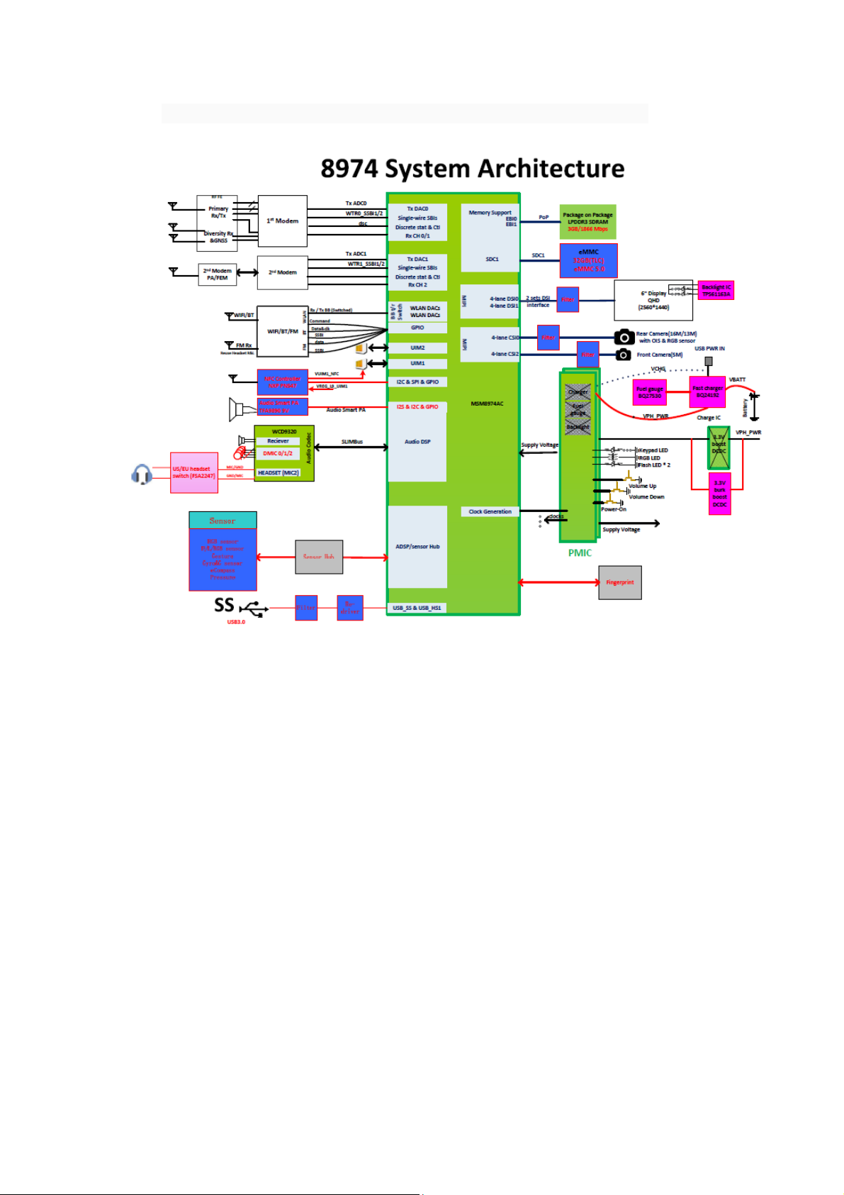
The following figure is a block diagram of the hardware design system.
The hardware of Z1 is composed of the main board, USB, Audio jake, volume
key FPC.
As shown below.
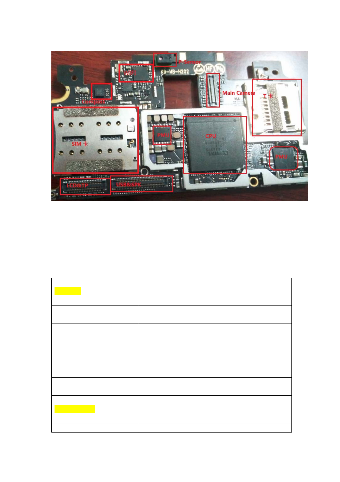
5
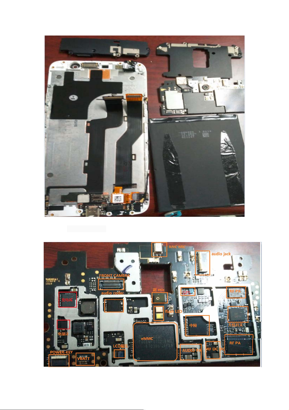
The following figure is marked major chip and functional distribution on the
main board.
6
4. Application processor
4.1.1 General Description
Feature MSM8974 capability
Processors
Applications Four Krait uP cores up to 2+ GHz; 2 MB L2 cache
Modem system QDSP6 v5 core at up to 600 MHz
16k L1 instruction; 32k L1 data; 256k L2 caches
RPM system Cortex M3 - primary boot processor
– better suited for code certification and warm boot
– brings up secure root of trust (SROT) Krait uP quickly
The only master of the modem power manager (MPM)
MPM coordinates shutdown/wakeup, clock rates, and VDDs
Boot flow is RPM / applications processor-based
Low power audio QDSP6 v5 core at 600 MHz; 16k/32k L1 and 256k L2
caches
WLAN/BT/FM ARM9
Memory support
Internal memory via PoP & EBI 2x LPDDR3 SDRAM; 32-bit wide; up to 800 MHz
Other internal memory 1.5 MB unified SRAM pool on-chip memory (OCMEM)
7

External memory
Via SDC1
Via SPI
eMMC NAND flash devices
NOR memory devices (user-modified SW)
RF support
RF operating bands Defined by WTR device
Air interfaces
GSM
WCDMA
LTE
WLAN/BT/FM
See 'Air interface features' section for details
Yes – all
Yes –,MSM8974AC
Yes – all (supported data rates depend upon MSM variant)
Yes –, MSM8974 AC
Yes – MSM8974 AC
Yes – all (with WCN3680B)
GNSS – gpsOne engine Gen 8B; GPS , GLONASS and Compass
Multimedia
Display support
MIPI_DSI
HDMI
eDP
Example combinations
General display features
Camera interfaces
MIPI_CSI
2D performance
3D performacne
General camera features
Up to three concurrent displays; two panels + external
Two; 4-lane + 4-lane
Yes; v1.4
Yes; v1.2 4-lane
2560x2048 + 1080p external
2048x1536 + 1920x1200 + 1080p external
2048x1536 + 4kx2k external
Color depth – 24-bit pp; TFT, LTPS, CSTN, OLED panels
Qcamera; dual ISP
Three 4-lane or four at 4 + 4 + 1 + 1 lanes; 1.5 Gbps per lane
32 MP at 15 fps; 16 MP at 30 fps
12 MP at 15 to 24 fps; 8 MP at 30 fps
Pixel manipulations, camera modes, image effects, and post
processing techniques, including defective pixel correction
VFE raw dump of CSI data at line rate
SMIA++ support
I2C or SPI controls
Mobile display processor MDP 5
Video applications performance
Encode
Decode
1080p at 120 fps; 4kx2k at 30 fps; 4x 1080p at 30 fps
– H.264/263, MPEG4, VP8
1080p at 60 fps 2-view – MVC
1080p at 120 fps; 4kx2k at 30 fps; 4x 1080p at 30 fps
– H.264/263, MPEG4/2, WMV9, VC1, VP6/8, DixX, XVID
1080p at 60 fps 2-view – MVC
Graphics Adreno 330 450 MHz 3D graphics accelerator
225 M peak triangles/sec; 3600 M peak 3D pixels/sec
APIs include OpenGL® ES 1.1/2.0/3.0, OpenCL1.2,
DX9.3
Audio
8

Codec
Low power audio
Voice codec support
Audio codec support
Enhanced audio
Integrated within the WCD9320 device
7 DACs, 8 outputs; 6 inputs, 6 ADCs; 6 digital MICs
Multi-button headset control; MIC activity detection
Low power, low complexity; 7.1 surround sound
Verstile – many audio playback & voice modes; encoders
for
audio & FM recording; many concurrency modes
SILK; QCELP, EVRC, EVRC-B, EVRC-WB;
G.711, G.729A/AB; GSM-FR, -EFR, -HR; AMR-NB, -WB
MP3; AAC, +, eAAC; WMA 9/Pro; Dolby AC-3, eAC-3,
DTS
Surround sound: Dolby TrueHD; DTS-HD; DTS Express
7.1
Fluence Noise Cancellation; enhanced speaker protection
QAudioFX™ / Qconcert™ / QEnsemble
A/V output – HDMI Rev 1.4a Yes
Integrated HDMI Tx core and HDMI PHY
1080p at 60 Hz refresh; 24-bit RGB color
Up to 8-ch audio for 7.1 surround sound
Dolby Digital Plus, Dolby True-HD, & DTS-HD Master
Web technologies V8 JavaScript Engine optimizations
Webkit browser JPEG hardware decode acceleration
Networking Stack IP and HTTP tuning
Flash 10.1 & Video Processor decode optimization
Messaging Text messages; text encoding for SMS
Multimedia messaging services – combined video
(MPEG4),
still image (JPEG), voice tag (AMR), text sent as message
Digital Mobile Broadcast (DMB) External IC required; dual TSIF for 12 segment ISDB-T
Connectivity
BLSP ports
UART
UIM
I2C
SPI (master only)
12, 4 bits each; multiplexed serial interface functions
Yes – up to 4 MHz
Yes – SIM, USIM, CSIM; dual V (1.8/2.85) is available 1x
Yes – cameras, sensors, near field communicator
Yes – cameras, sensors, etc; NOR memory with SW mods
UIM (other than via BLSP) One – dual voltage (1.8/2.85)
USB Two USB 2.0 high-speed and One USB 3.0 super-speed
HSIC
Dual-voltage (1.2/1.8)
Secure digital interfaces
SDC1 and SDC2 are dual-V
MSM to/from external application processor
Easy integration, low-power, & low processor loading
Up to 4 ports; one 8-bit and three 4-bit; SD3.0
SD/MMC card; eMMC NAND; DMB; WLAN; eSD/eMMC
boot
TSIF Up to two ports; DMB support
Audio interfaces
9
SLIMbus
I2S
MI2S
PCM
Highly multiplexed, high-speed; baseline WCD interface
Up to 4 ports (primary & seconday speakers & mics)
Microphone & speaker functions, including 7.1 audio for
HDMI
One port is available
Wireless connectivity
WLAN
Bluetooth
WCN3680B
Both WCNs support 802.11a/b/g/n/ac; BT 4.0 LE and earlier
Worldwide broadcast
Touchscreen support Capacitive panels via ext IC (I2C, SPI, & interrupts)
DMB support Via external DMB device (SDC or TSIF)
Configurable GPIOs
Number of GPIO ports 146 – GPIO_0 to GPIO_145
Input configurations Pull-up, pull-down, keeper, or no pull
Output configurations Programmable drive current
Top-level mode multiplexer Provides a convenient way to program groups of GPIOs
Internal functions
Security
General security features
Crypto engine
QFPROM
Security controller
Secure boot, SFS, OMA DRM 1.0/2.1, ARM TrustZone,
SEE,
secure debug, Microsoft WM DRM10, HDCP for HDMI
V4; algorithm accelerate file system encryption (AES-XTS)
and IPSec & SSL (HMAC-SHA, CCM, CBCMAC)
Large fuse array, replaces previous-generation Qfuse chains
Non-volatile memory with faster and simpler programming
Chip-wide configuration for security, feature enable, &
debug
Persistent storage of ID numbers and sensitive key data
Support for the HDCP standard needed for HDMI
Secure HDCP key provisioning and secure debug facility
Gateway for all software and JTAG accesses to the
QFPROM
Primary and secondary hardware key blocking for SFS
Boot sequence 1) RPM system, 2) application system, 3) modem system
Emergency boot over HS-USB (on USB 3.0 port)
Power-on boot to carrier splash screen < 0.4 seconds (target)
Power-on boot to network access < 20 seconds (target)
PLLs and clocks Multiple clock regimes; watchdog & sleep timers
Inputs: 19.2M CXO, 48M WCN_XO for 5 GHz WLAN,
General-purpose outputs: M/N counter, PDM
Resource and power manager Fundamental to bootup and power management
Key blocks: RPM core, Cortex M3, security controller,
MPM
Improved efficiency via clock control, split-rail power
10

collapse
& voltage scaling; several low-power sleep modes
Debug JTAG, Design for Software Debug (DFSD), & ETM (all
cores)
Others Thermal sensors; modes & resets; perhiperal subsystem
Chipset and RF front-end (RFFE) interface features
WTR RF transceivers
Baseband data
Status & control
Power management 2-line SPMI; plus other lines as needed via GPIOs
WCD audio codec
SLIMbus
Legacy
Others
WCN wireless connectivity
WLAN baseband data
WLAN status & control
Bluetooth
Fabrication technology and package
Digital die 28 nm HPm CMOS
Small, thermally efficient
package
Bottom pin array of PoP Same as 990-pin nanoscale pkg (990 NSP); 0.4 mm pitch
Top pin array of PoP Same as 216-pin chipscale pkg (216 CSP); 0.5 mm pitch
4 Rx & 2 Tx analog interfaces
2 SSBIs for each RFIC plus other lines as needed via GPIOs
Highly muxed, high-speed audio data plus status & control
Optional I2S for audio data plus I2C for status & control
Status, control, & clock lines as needed via GPIOs
Multiplexed Rx/Tx analog interface
Secure digital
2-line data interface plus dedicated SSBI
990 PNSP: 15 x 15 x 0.91 mm (w/o memory device on top)
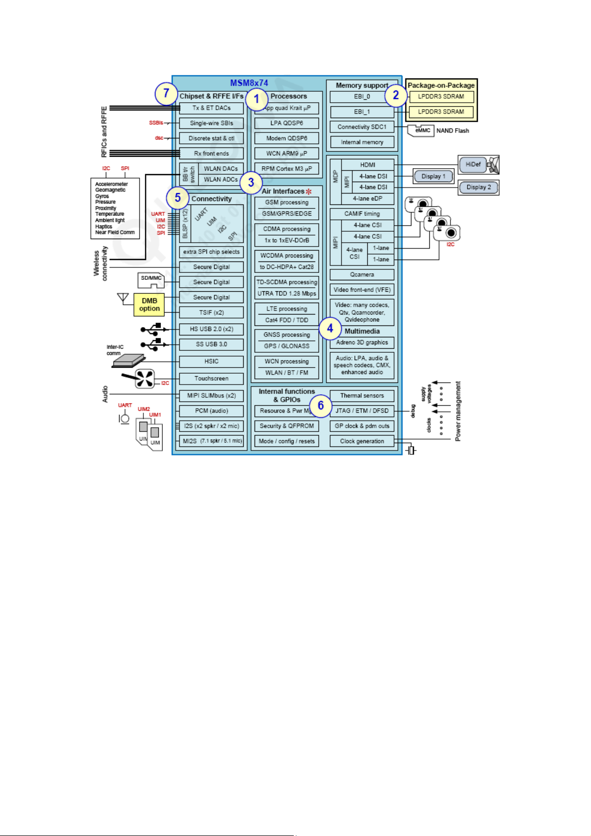
4.1.2 Block Diagram
The following block diagram of MSM8974AC.
11
5. Power Management
5.1.1 Block Diagram
PM8941 have five major functional blocks:
1) Input power management
2) Output power management
3) General housekeeping
4) User interfaces
5) IC-level interfaces
12
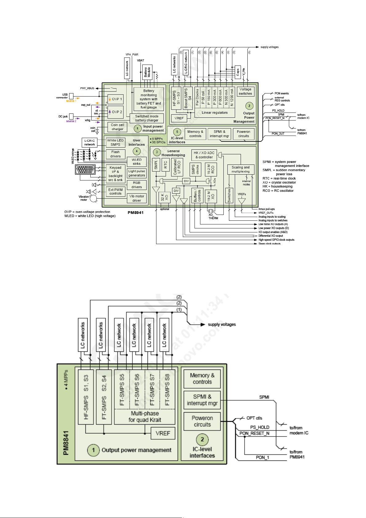
PM8841 have two major functional blocks:
1) Output power management
2) IC-level interfaces
13
 Loading...