

Lenovo L2262W Service Manual
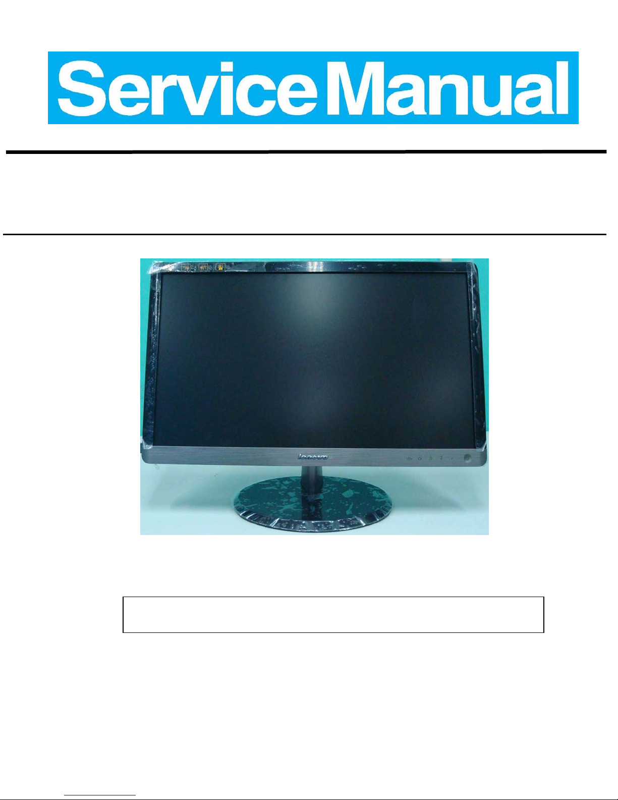
Lenovo Service Manual L2262W
1
联想显示器维修手册
Custom: Lenovo
Model: L2262W
This manual apply to MainBoard715G4567
(IC SCALER TSUMU58PWHL)
Lenovo Service Manual L2262W
2
REVISION LIST
Version Release Date Revision History Model TPV Model No Editor
A00 Sep-28-2010 Initial Release L2262W
TIAMSQ6YZQG1HNJ
TIAASQ6YZQG1HNJ
TPV-BJ-Rainsun
A01 Mar-25-2011
Update Disassembly
SOP and soft SOP
L2262W
TIAMSQ6YZQG1HNJ
TIAASQ6YZQG1HNJ
TIAMSQ6YZQG1HNJ
TIAASQ6YZQG1HNJ
TIAASQ6YZQG2HNJ
TIAGSQ6YZQG1HNJ
TIAGSQ6YZQG2HNJ
TIAMSQ6YZQG2HNJ
TIAMSQ6YZQG1H2J
TIAMSQ6YZQG2H2J
TIBMSQ6YZQG3H2J
TIBGSQ6YZQG3HNJ
TIBASQ6YZQG2HNJ
TPV-BJ-Rainsun

Lenovo Service Manual L2262W
3
CONTENTS
1. LCD Specifications 4
1.1 Product Features ......................................................................................................................................................................... 4
1.2 New Features .............................................................................................................................................................................. 4
1.3 Factory preset modes.................................................................................................................................................................. 5
2. Operation instruction 6
2.1 Control Buttons ........................................................................................................................................................................... 6
2.2 OSD User mode adjustment ........................................................................................................................................................ 7
2.3 OSD Lock function ..................................................................................................................................................................... 10
3.Interface description 11
3.1 VGA Interface description ......................................................................................................................................................... 11
3.2 DVI Connector ........................................................................................................................................................................... 11
4. Panel Feature 12
4.1 General information ................................................................................................................................................................. 12
4.2 Absolute Maximum Ratings ...................................................................................................................................................... 12
4.3 Electrical Characteristics ........................................................................................................................................................... 12
4.4 Optical Characteristics .............................................................................................................................................................. 13
4.5 Panel Block Diagroam ............................................................................................................................................................... 14
4.6 LVDS Connector pin Assignment ............................................................................................................................................... 14
4.7 Lightbar Connector pin Assignment .......................................................................................................................................... 15
5.Block Diagram 16
5.1 LCD Block Diagram .................................................................................................................................................................... 16
5.2 MainBoard Block Diagram ........................................................................................................................................................ 16
5.3 Power/ Inverter Board Block Diagram ...................................................................................................................................... 17
5.4 Software Flow Chart ................................................................................................................................................................. 19
6. Circuit Schematic 20
6.1 Main Board---715G4567-M ...................................................................................................................................................... 20
6.2 Power Board 715G2892-P01 ................................................................................................................................................. 24
6.3 Converter board---715G4107 .................................................................................................................................................... 25
6.4 Key Board 715G4572-KOA ..................................................................................................................................................... 26
7.Exploded V iews 27
8. PCB Layout 28
8.1 MainBoard- 715G4567-M ....................................................................................................................................................... 28
8.2 PowerBoard 715G2892-P01-020 .............................................................................................................................................. 31
8.3 KeyBoard 715G4572-K0A .......................................................................................................................................................... 32
9. Maintenance 33
9.1 Maintenance requisite .............................................................................................................................................................. 33
9.2 Disassembly SOP ....................................................................................................................................................................... 33
9.3 Trouble Shooting ....................................................................................................................................................................... 37
9.4 Software update step(SOP) ................................................................................................................................................. 43
9.5 Re-writing DDC program step ................................................................................................................................................... 48
9.6 Factory mode adjustment ......................................................................................................................................................... 51
10.BOM List 53
10.1 Model:TIAMSQ6YZQG1HNJ ................................................................................................................................................. 53
Lenovo Service Manual L2262W
4
1. LCD Specifications
1.1 Product Features
Model Lenovo L2262W
LCD Panel
Driving system TFT Color LCD
Active Display Area 546.86mm(21.53”) 479.8 (W)×271.3(H)mm
Pixel Pitch 0.248 mm×0.248mm
Input
Video
R,G ,B Analog Interface,75ohm,0.7V Positive
DVI digital Interface
Separate Sync. H/V TTL
H-Frequency 30kHz--83kHz
V-Frequency 50Hz--76Hz
Input Connector
D-Sub 15pin
DVI 24pin
Display Colors 16.7M Colors
Dot Clock 210MHz /165MHz
Max. Resolution 1920x1080 @60Hz
Plug & Play VESA DDC2B DDC/CI
Power Consumption
ON Mode <27W
Power Saving Mode <1W at 100Vac & 240Vac
Switch OFF
<0.5W
Power Source
90~264VAC,47~63Hz, 1.5A Max supply current
Environmental
Considerations
Operating Te mp: 0° to 40°C
Storage Temp.: -20° to 60°C
Operating Humidity : 8% to 80%
Dimensions(including stand)
369.9(W)x386.0(H)x146.5 (D)mm
Weight (N. W.): 3.73kg
Safety/EMI
GB4943 IEC60950 CE CCC RoHS
1.2 New Features
With LED backlight of the Panel, 6 Touch Control buttons ,
HDCP Support, Digital Controls with 8 languages OSD;
Lenovo Service Manual L2262W
5
1.3 Factory preset modes
STANDARD RESOLUTION
HORIZONTAL
FREQUENCY
VERTICAL
FREQUENCY
VGA
640×480
31.469kHz 59.94Hz
640×480
35.00kHz 66.67Hz
640×480
37.861kHz 72.80Hz
640 × 480 37.50kHz 75.00Hz
DOS-mode
640 × 480 31.469kHz 70.087Hz
720 × 400 31.469kHz 70.087Hz
Mac-mode 832 ×624 49.725kHz 74.50Hz
SVGA
800 × 600 35.16kHz 56.25Hz
800 × 600 37.879kHz 60.317Hz
800 × 600 48.07kHz 72.188Hz
800 × 600 46.875kHz 75Hz
XGA
1024 × 768 48.363kHz 60Hz
1024 × 768 56.476kHz 70Hz
1024 × 768 60kHz 75Hz
1152 × 864 67.6kHz 75Hz
1280 x 1024
63.981kHz
60.020 Hz
1280 x 1024
74.882 kHz
69.853 Hz
1280 x 1024
79.976 kHz
75.025 Hz
WXGA
1440 x 900
55.935 kHz
59.887 Hz
1440 x 900
55.469 kHz
59.901 Hz
1440 x 900 70.635kHz 74.984
1600 × 900 60.00kHz 60Hz
1600 × 900 70.463kHz 74.96Hz
1680x1050
64.674kHz
59.883Hz
1680x1050 65.29kHz
59.95Hz
1680x1050
82.31kHz
74.89Hz
Full HD
1920x1080
66.58kHz
59.93Hz
1920x1080
67.5kHz
60Hz
Lenovo Service Manual L2262W
6
2. Operation instruction
Generalization
Press the power button to turn the monitor on or off.
The other control buttons are loca ted at front pane l of the monitor. By changing these sett ings, the pictur e can be
adjusted to your personal preferences.
The power cord should be connected.
Connect the video cable from the video card of PC to the monitor.
Press the power button to turn on the monitor, the power indicator will light up.
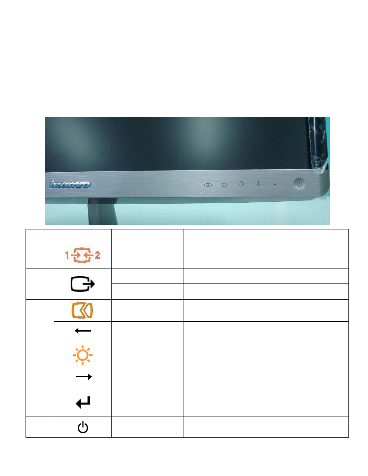
2.1 Control Buttons
Icon Control Description
1
Input select Switches the video input source.DVI/D-SUB
2
DDC-CI Pressed till 10 seconds, will enable/disable the DDC/CI.
Exit Exit current OSD return to last level.
3
Auto Adjustment If there is no any OSD, it is auto configuration.
Decrease - adjusting
OSD, it will decrease curre nt value of bar, or move to last
item of menu.
4
NOVO VISION If there is no any OSD,Direct access to Imange Properties
Increase + adjusting
OSD, it will increase curre nt value of bar, or move to next
item of menu.
5
Menu
/Enter/OK
Active main m enu whil e no OSD dis pla y,enter next level on
main menu or sub menu status, or enter last level on
adjustment bar.Continued pressing 10 seconds will lock
menu or un-lock menu.
6
Power Button Power ON/OFF,and power indicator(Blue and Orange).
Lenovo Service Manual L2262W
7
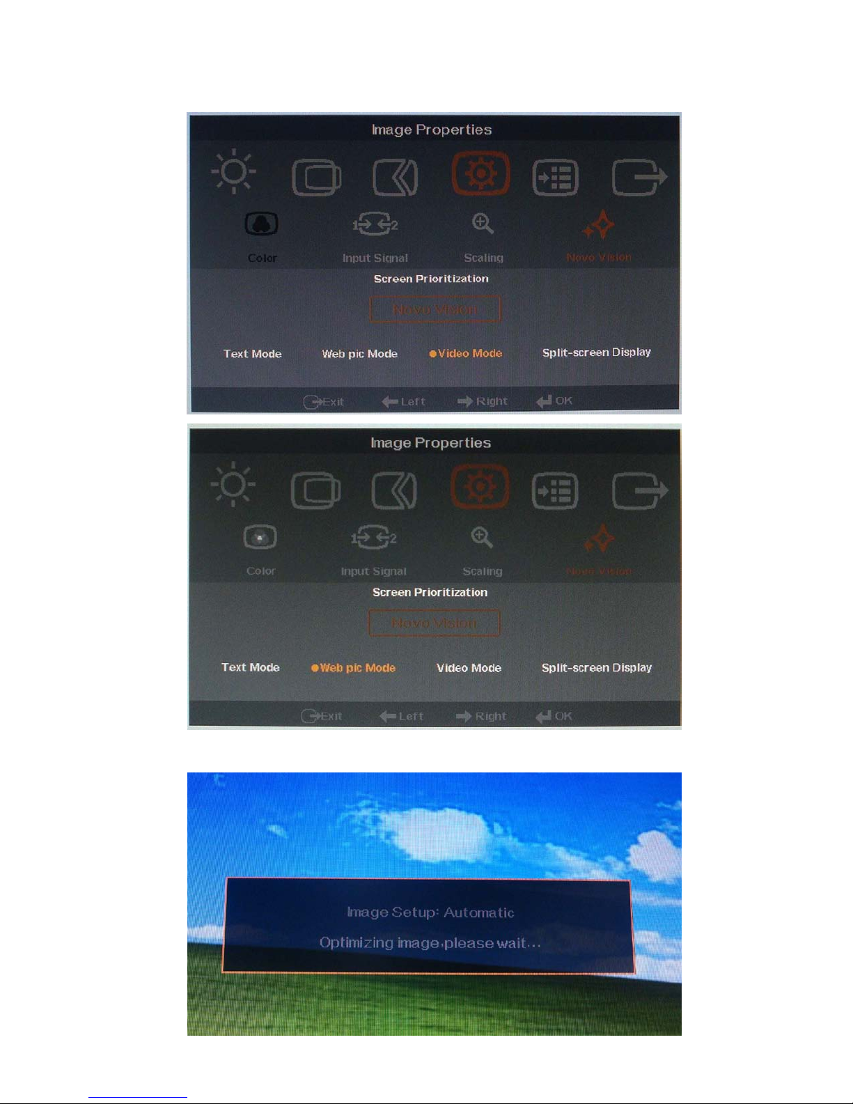
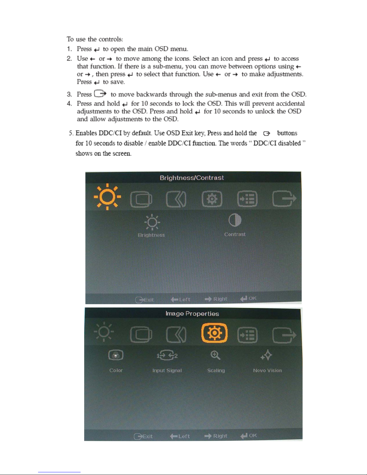
2.2 OSD User mode adjustment
a)Hot key
Press
▶,the figure is as shows
Press ◀,the figure is as shows
Lenovo Service Manual L2262W
8
b)OSD Menu adjustment steps:
Lenovo Service Manual L2262W
9
Lenovo Service Manual L2262W
10
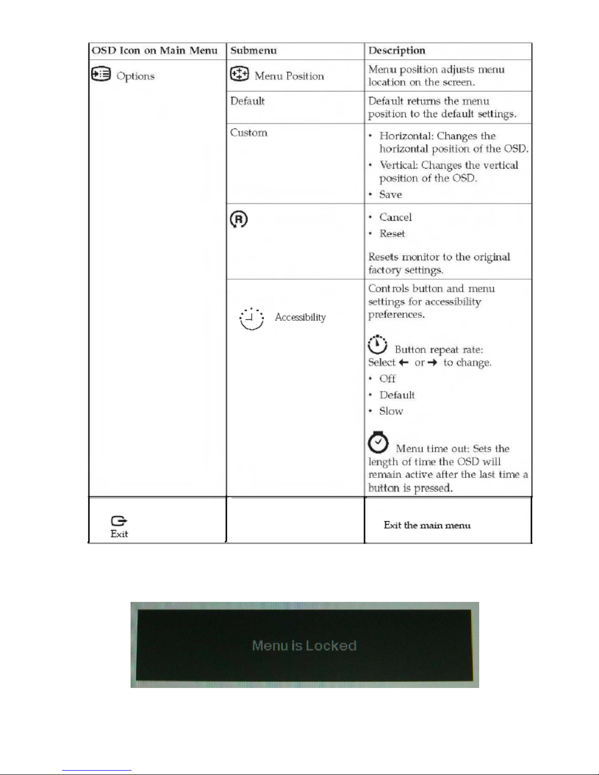
2.3 OSD Lock function
Press “MENU” button and hold 10s,OSD was locked.Again Press “MENU” button and hold 10s,OSD was unlocked.
Lenovo Service Manual L2262W
11
3.Interface descripti on
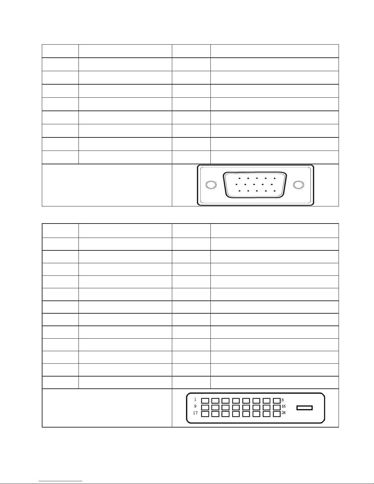
3.1 VGA Interface description
Pin No. Description Pin No. Description
1. Red Input 9. +5VDC
2. Green Input 10. GND
3. Blue Input 11. GND
4. GND 12. SDA- DDC-Serial Data
5. Connection detect 13. H Sync
6. Red GND 14. V Sync
7. Green GND 15. SCL- DDC-Serial Clock
8. Blue GND
VGA Connector layout
1
5
6
10
11
15
3.2 DVI Connector
Pin No. Description Pin No. Description
1. TMDS Data 2- 13. TMDS Data 3+
2. TMDS Data 2+ 14. +5V Power
3. TMDS Data 2/4 Shied 15. Ground (for +5V)
4. TMDS Data 4- 16. Hot Plug Detect
5. TMDS Data 4+ 17. TMDS Data 0+
6. DDC Clock 18. TMDS Data 0-
7. DDC Data 19. T MD S Data 0/5 Shield
8. N.C. 20. TMDS Data 5-
9. TMDS Data 1- 21. TMDS Data 5+
10. TMDS Data 1+ 22. TMDS Clock Shield
11. TMDS Data 1/3 Shield 23. TMDS Clock+
12. TMDS Data 3- 24. TMDS Clock-
DVI Connector layout
Lenovo Service Manual L2262W
12
4. Panel Feature
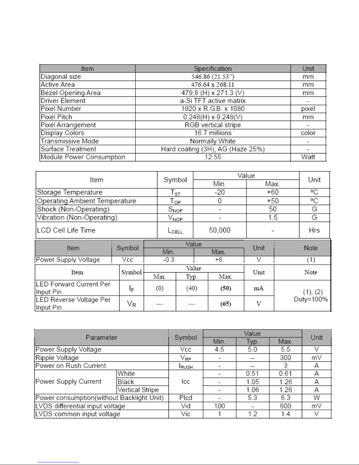
The Panel is a 21.5 inch color TFT-LCD module—M215H3-LA1 . This module supports 1920×1080 Full HD(16:9)
mode and displays up to 16.7 millions colors.This model is composed of a TFT LCD panel,a driver circuit andwith LED
back light unit .
4.1 General information
4.2 Absolute Maximum Ratings
4.3 Electrical Characteristics
a) TFT LCD module
Lenovo Service Manual L2262W
13
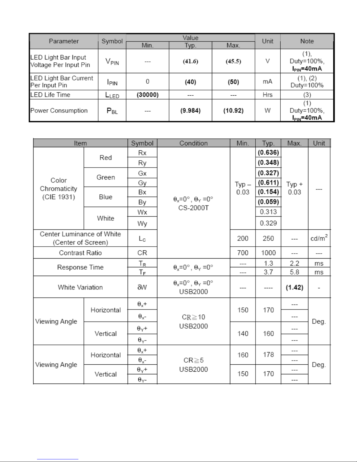
b) Backlight unit
4.4 Optical Characteristics
Lenovo Service Manual L2262W
14
4.5 Panel Block Diagroam
4.6 LVDS Connector pin Assignment

Lenovo Service Manual L2262W
15
4.7 Lightbar Connector pin Assignment
Lenovo Service Manual L2262W
16
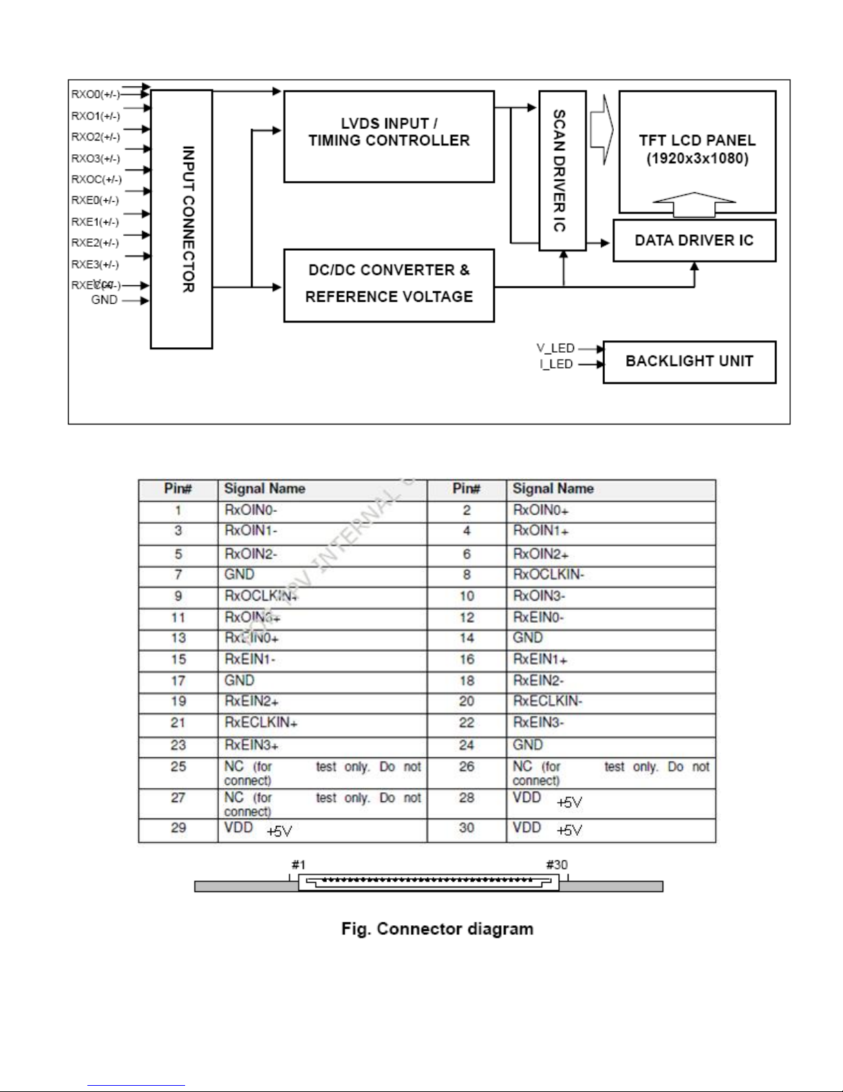
5.Block Diagram
5.1 LCD Block Diagram
5.2 MainBoard Block Diagram
DC-AC inverter
AC-DC
(5V/12V)
Power Board
Main Board
Key board
Computer
VGA
LED backlight
Panel LVDS
AC supply
90V-264V
LCD Block Diagram
Input signal
Computer
DVI
Crystal 14.318MHZ
(X401)
Panel Interface
(CN406)
Scalar TSUMU58PWHL-LF-1 Mstar
(Include ADC, OSD, MCU)
(U401)
D-Sub
Connector
(CN101)
EEPROM
MX25L2026DM1I
(U402)
H sync
V sync
Key Board
Control
(CN401/402)
Voltage converter
5V
5V 3.3V 1.8V
DVI
Connector
(CN102)
From PC
Lenovo Service Manual L2262W
17
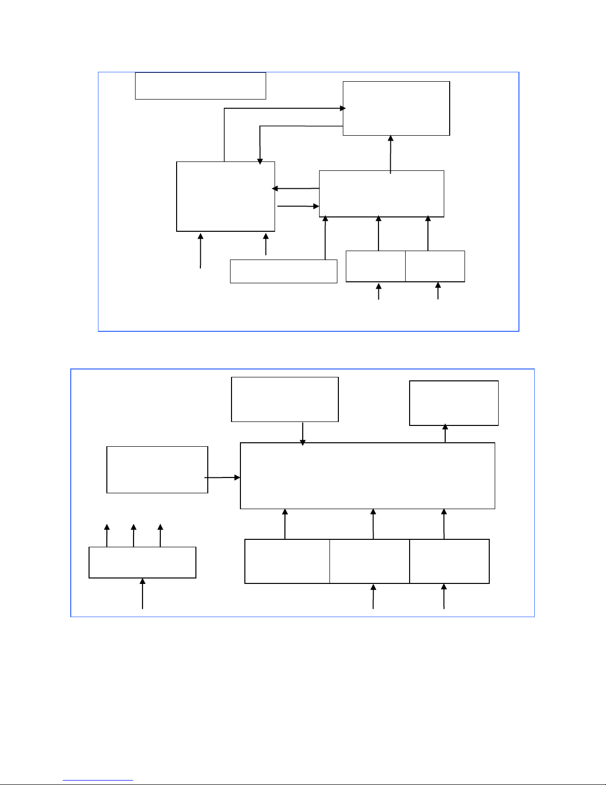
5.3 Power/ Inverter Board Block Diagram
Fuse EMI
Rectifier
Smoothing
Capacitor
C907
Transformer
T901
MOS
Q901
IC-PWM
IC901
12V
Rectifier
5V
Rectifier
12V
5V
Sense
resistor
Vcc
Rectifier
regulating
Sampling
PhotoCoupler
Vcc
Open Lamp Protection
12V DC
IC Power Supply
Converter
DC-AC
Transformer
T801
High Voltage
Output
Resonance NET
Switching MOS
Q802-AM9945
AC input
100-240V
2- CCFL
PWM Control IC
IC801-TL494
Current Sampling
Power part
Inverter part
Lenovo Service Manual L2262W
18
Fuse
EMI
Rectifier
Smoothing
Capacitor
Transformer
T901
MOS
Switching
IC-PWM
IC901
12V
Rectifier
5V
Rectifier
12V
12V
5V
Sense
resistor
Vcc
Rectifier
regulating
sampling
photocoupler
Vcc
Converter
Vout30V
CN801
Switching MOS
Q801
AC input
100-240V
CN803
Current Sense
LED converter Part
Power adapter Part
On/off DIM
PWM Control
IC801
12V
Power/ Converter Board Block Diagram
SET
Lenovo Service Manual L2262W
19
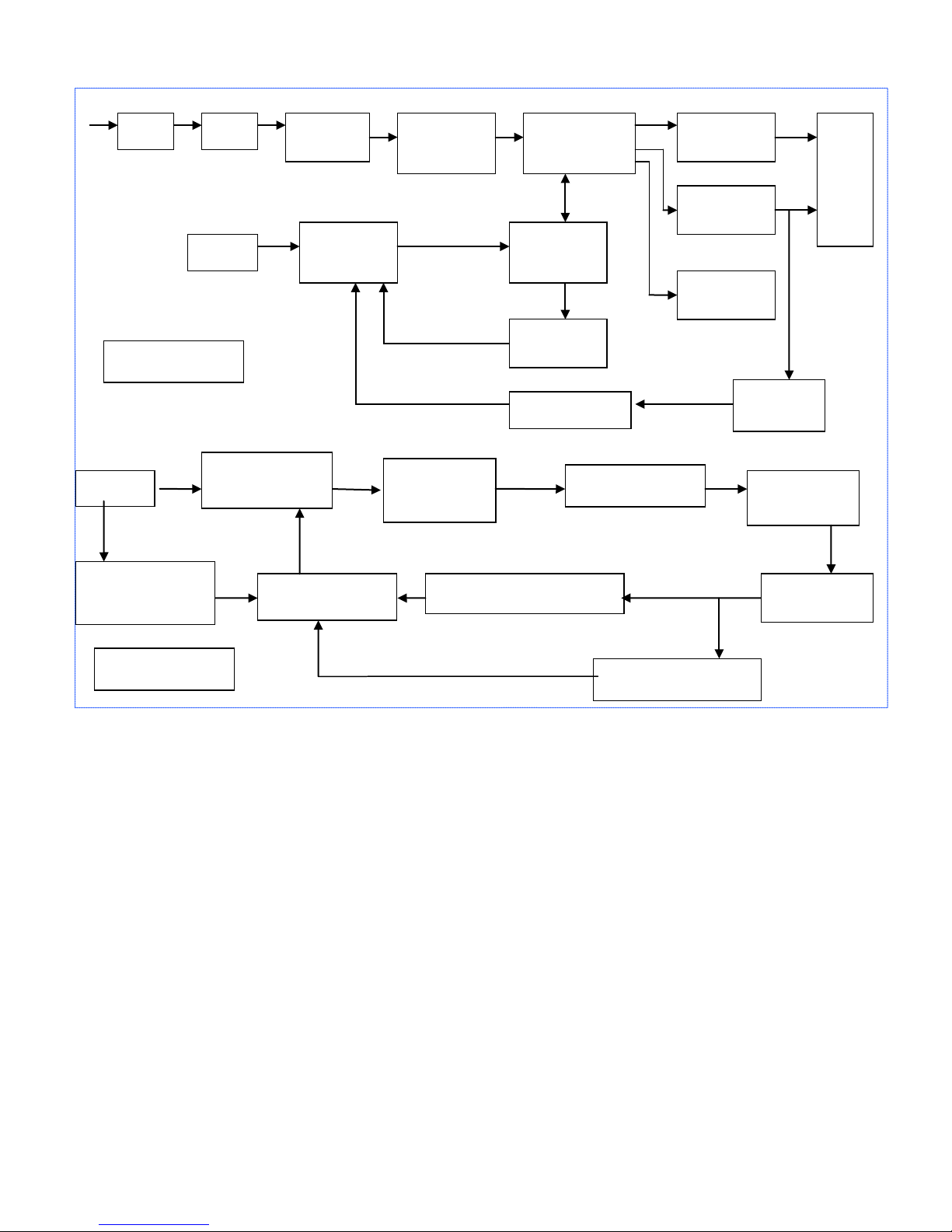
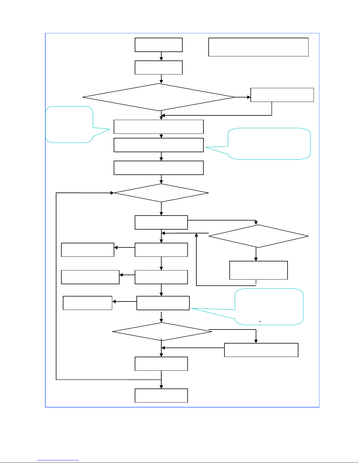
5.4 Software Flow Chart
------Just for your reference.
Start
Initial_MCU
Check if DataBuffer Is blank
Check if Sum is changed ?
To Write default values
Read parameter_from Buffer
PowerHandler
Init_GlobalVariables
Initial_MCU Device
while
InputTiming
ModeHandler
MenuHandler
DebugHandler
if standby mode?
Brightness
Contrast
Language
InputType
InputTimingStableCounter
OsdCounter
PowerDownCounter
LED turn-on
Show power on logo
if factory mode?
No signal message
UnsupportModeFlag
END
OSD Menu
Software Flow Chart
InputTiming
Phaes/Frequency
Image setup
Color
Enter factory mode OSD
Y
N Y

Lenovo Service Manual L2262W
20
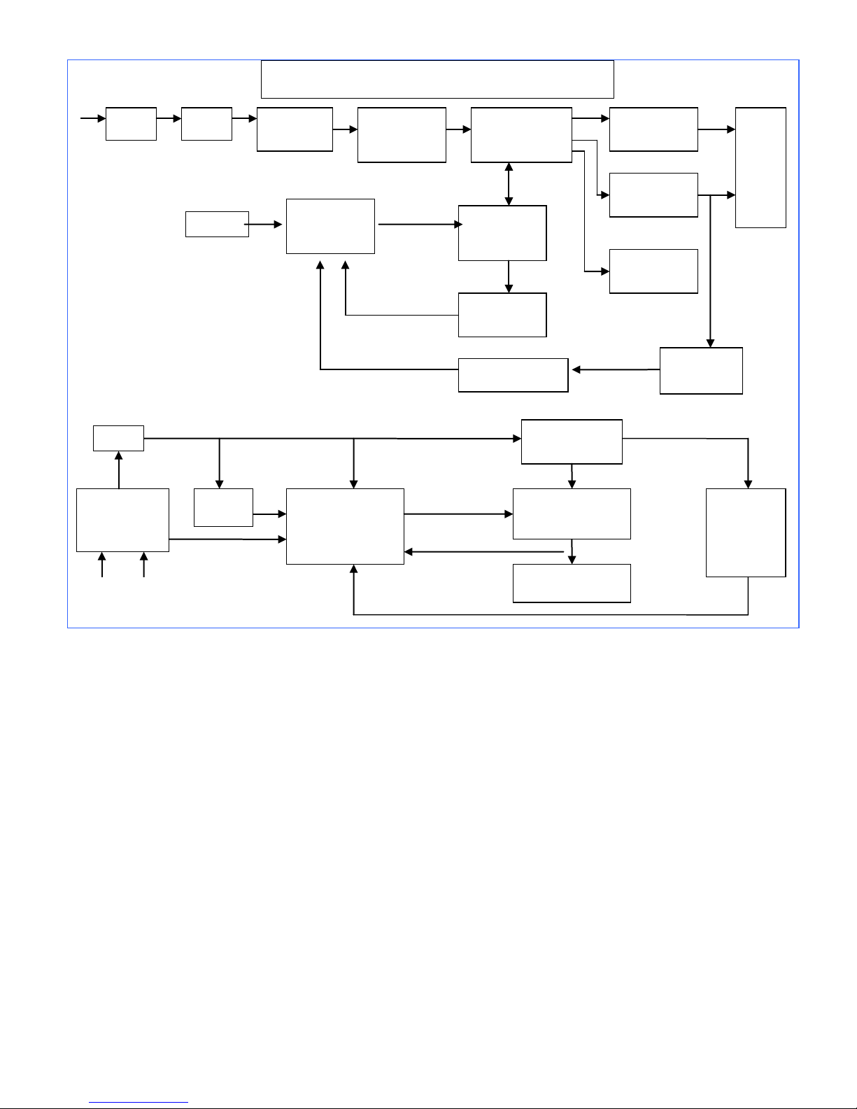
6. Circuit Schematic
6.1 Main Board---715G4567-M
DSUB_SOG [5]
R101
100R 1/16W 5%
R120 1K 1/ 16W 5%
R129 10R 1/16W 5%
R134 10R 1/16W 5%
FB104
300 OHM
R136
4K7 1/16W 5%
FB105
300 OHM
HDCP_CTRL [ 5]
H_Sy nc
DDC2_SDA
DSUB_R+ [5]
C120
NC
GND POWER
DDC2_SCL [5]
R117 47 OH M 1/16W
DDC2_SDA
R114 47 OH M 1/16W
ESD_VCC
H_Sy nc
DSUB_SDA
R118 100R 1/ 16W 5%
FB102
BEAD
1 2
CMVCC1
DDC2_SCL
C119
NC
VGA_G-
CMVCC1[3,4,5]
DVI_HPD
RXCN
DGND
DDC1_SCL
DVI_5V
U101
AT24C02BN-SH-T
1
2
3
45
6
7
8
A0
A1
A2
GNDSDA
SCL
WP
VCC
VGA_R+
U105
AZC199-04S
1
2
3 4
5
6
I/O1
GND
I/O2 I/O3
VDD
I/O4
R140
NC
候綼U101
RX1 N [5]
C106
0.047uF
R121
NC
VGA_B+
VGA_PLUG
FB103
BEAD
1 2
R130 10R 1/16W 5%
R111 10OH M1/16W
ESD_VCC1
VGA_B+
C116
220N16V
R109 47 OH M 1/16W
R128 10R 1/16W 5%
R102 0R05 1/10W 5%
候綼U103
DSUB_B+ [5]
U102
AT24C02BN-SH-T
1
2
3
45
6
7
8
A0
A1
A2
GNDSDA
SCL
WP
VCC
C112
NC
C114
0.047uF
R113
100R 1/16W 5%
DDC1_SCL[5]
RXCN [5]
RX1 N
VGA_R+
R123
4K7 1/16W 5%
ESD_VCC1
C109
5pF/50V
DSUB_V [5]
DDC2_SCL
Q101
NC
U103
AZC199-04S
1
2
3 4
5
6
I/O1
GND
I/O2 I/O3
VDD
I/O4
R132 10R 1/16W 5%
R116
75R 1/16W 5%
FB110
300 OHM
VGA_G+
C104
22pF
CN101
1
6
2
7
3
8
4
9
5
11
12
13
14
15
10
17
16
C118
NC
D104
BAV70
3
1
2
V_Sync
DVI_5V
RX2 P [ 5]
DDC1_SDA[5]
RXCP
候綼U107
RX0 N
C108
0.047uF
DVI_HPD
R105 10OH M1/16W
C115
0.1uF/16V
R139
6K8 1/16W 5%
ESD_VCC
U104
AZC199-04S
1
2
3
4
5
6
I/O1
GND
I/O2 I/O3
VDD
I/O4
C124
0.1uF/16V
ESD_VCC2
ESD_VCC2
候綼U106
VGA_R-
VGA_B+
VGA_G-
R126 10R 1/16W 5%
DSUB_B- [5]
C111
0.047uF
ZD104
RLZ5.6B
RXCP [5]
VGA_B-
候綼U105
RX0 P [ 5]
C110
0.047uF
RX2 N [5]
R135
10K 1/16W 5%
DET_CABLE
[5]
VGA_G+
DSUB_R- [5]
V_Sync
DDC1_SDA
DDC1_SCL
R107
2K2 1/16W 5%
DSUB_SDA
R122
NC
DSUB_G- [5]
R115 10OH M1/16W
R124
4K7 1/16W 5%
DDC2_SDA [5]
C117
220N16V
R112
75R 1/16W 5%
DDC1_SDA
D108
BAV70
3
1
2
R133
10K 1/16W 5%
ESD_VCC
VGA_G+
CN102
CONN
1
2
3
4
5
6
7
8
9
10
11
12
13
14
15
16
17
18
19
20
21
22
23
24
26
25
DAT2-
DAT2+
2/4shield
DAT4-
DAT4+
DDC SCL
DDC SDA
VSYNC
DAT1-
DAT1+
1/3shield
DAT3-
DAT3+
+5V
SYNC GND
HPD
DAT0-
DAT0+
0/5shield
DAT5-
DAT5+
clk shield
clk+
clk-
GND
GND
R138
4K7 1/16W 5%
RX1 P [ 5]
VGA_R+
RX2 P
R131 10R 1/16W 5%
R106
2K2 1/16W 5%
C103
22pF
DSUB_SCL
RX1 P
C102
0.047uF
DVI_1_5V
VGA_B-
U106
AZC199-04S
1
2
3 4
5
6
I/O1
GND
I/O2 I/O3
VDD
I/O4
C101
NC
DVI_1_5V
C105
5pF/50V
U107
AZC199-04S
1
2
3 4
5
6
I/O1
GND
I/O2 I/O3
VDD
I/O4
DSUB_G+ [5]
DSUB_5V
DSUB_H [5]
ESD_VCC2
VGA_PLUG
R127 10R 1/16W 5%
R137
4K7 1/16W 5%
VGA_R-
C121
1000pF
R119 100R 1/ 16W 5%
ESD_VCC1
Lenovo L2262 1
Lenovo L2262
Custom
2 5Saturday , J uly 24, 2010
<
称爹>
2.0.INPUT
OEM MODEL Size
Rev
Date
Sheet
of
TPV MODEL
PCB NAME
称爹
T P V ( Top Victory Electronics Co . , Ltd. )
Key Component
絬 隔 瓜 絪 腹
DDC_WP[5]
C113
5pF/50V
RX2 N
RX0 P
VCC3.3
DSUB_5V
R125
4K7 1/16W 5%
RX0 N [5]
VGA_PLUG
R110 470 OH M 1/16W
C122
1000pF
R103 1K 1/ 16W 5%
C107
1000pF
R108
75R 1/16W 5%
DDC_WP[5]
DSUB_SCL
FB101
BEAD
1 2
R104 1K 1/ 16W 5%
CMVCC1
DVI+VGA input part---+DDC
 Loading...