

Lenovo L2021 Service Manual
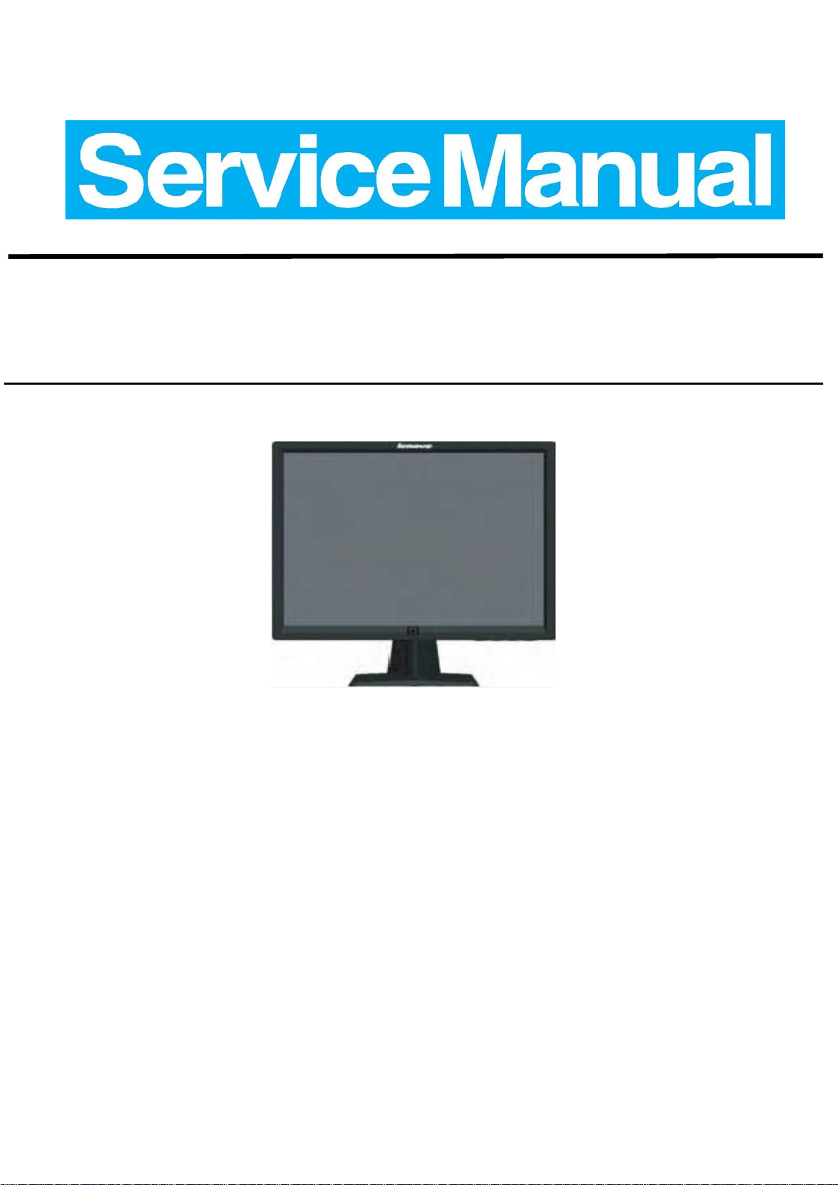
Lenovo Service Manual L2021W
联想显示器维修手册
rand:
B
enovo
L
Model: L2021 Wide
L2021WA
1
Lenovo Service Manual L2021W
REVISION LIST
Version
A00 May-15-2010 Initial Release L2021W TAASRJEYXAG1HNJ TPV-BJ-Rain
Release
Date
Revision
History
Model TPV Model No
Editors
Redactor
TAASRJEYXAG1HNJ
TAAMRJEYXAG1HNJ
TAASRJEYXAG1H2J
TPV-BJ-Rain
A01 Aug-30-2011 Update Part 9
L2021W
L2021WA
2

Lenovo Service Manual L2021W
CONTENTS
1. LCD Specifications .......................................... ................ ................ ................ .......... 4
1.1 Product Features ............................................................................................................................ 4
1.2 Factory preset modes ............................ ... ...................................................................................... 5
2.Operation instruction ................................................................................................. 6
2.1 Control Buttons ........................... ........................................................ .. ......................................... 6
2.2 OSD User mode adjustment .......................................................................................................... 7
3.Interface description ...................................................................................... ........... 11
3.1 VGA Interface description .......................................................................................................... 11
3.2 DVI Interface description ........................................ ......................................................... ........... 11
4. Panel Feature ........................................................................................................... 12
4.1 General Specifications ................................................................................................................. 12
4.2 Absolute Maximum Ratings ........................................................................................................ 12
4.3 Electrical Characterist ics ........................................................ .................................................... 13
4.4 Panel Block Diagroam ........................ .. ...... ..... ... ..... ..... ... ..... ... ..... ...... .. ...... .. ...... ..... ... ..... ............ 14
4.5 LVDS Connector pin Assignment .............................. .......................................................... ... .... 14
5.Block Diagram .......................................................................................................... 15
5.1 LCD Block Diagram ............................... ..... ... ..... ...... .. ...... .. ...... ..... ... ..... ... ..... ..... ... ..... ...... .. ....... 15
5.2 MainBoard Block Diagram ............................................. ..... ... ..... ...... .. ...... ..... ... ..... ..... ... ..... . ...... 15
5.3 Power/ Inverter Board Block Diagram ...................................................................................... 16
5.4 Software Flow Chart .................................................................................................................... 17
6. Circuit Schematic .................................................................................................. 18
6.1 Main Board---715G3327-1 .......................................................................................................... 18
6.2 Power Board715G4174-2 ............................................................................................................. 23
6.3 Inverter part ................................................................................................................................. 24
6.4 Key Board715G3248/715G3249 .................................................................................................. 25
7.Explore Views ............................................................................................................ 26
8. PCB Layout .............................................................................................................. 27
8.1 MainBoard- 715G3327-1 ............................................................................................................ 27
8.2 PowerBoard 715G4174 ................................................................................................................ 29
8.3 KeyBoard ...................................................................................................................................... 31
9. Maintenance ........................................................................................................... 32
9.1 Maintainability Requirement ..................................................................................................... 32
9.2 Disassembly SOP ........................................................... ............................................................... 32
9.3 Trouble Shooting ........................................... ........ ........... ........... .......... ........ ........... .................... 37
9.4 software update step .................................................................................................................... 42
9.5 Writing DDC program step ................ .. ........................................................... ... ......................... 48
9.6 Factory mode adjustment ........................................ ... ................................................................. 51
10.BOM List ................................................................................................................. 53
10.1 Model:TAASRJEYXAG1HNJ ............................................................................................... 53
3
Lenovo Service Manual L2021W
1. LCD Specifications
1.1 Product Features
Model Lenovo L2021Wide / L2021WA
Driving system TFT Color LCD
LCD Panel
Max. Resolution 1600 x 900@75Hz
Display Colors 16.7M Colors
Input
Input Connector
Dot Clock 160MHz
Plug & Play VESA DDC/CI
Active Display Area
Pixel Pitch
Video
Separate Sync. H/V TTL
H-Frequency 30kHz--80kHz
V-Frequency 60Hz--75Hz
442.8 (W)×249.07(H)mm 508.0mm(20.0”)
0.2768 mm×0.2768mm
R,G,B Analog Interface,75ohm,0.7V
DVI Digital Interface 150mV~1200mV
D-Sub 15pin
DVI 24pin
Positive
ON Mode <27W
Power Consumption
Power Source
Environmental
Considerations
Dimensions(including stand)
Weight (N. W.): 4.20kg
Safety approval
Power Saving Mode <1W at 100Vac & 240Vac
Switch OFF
<0.5W
90~264VAC,47~63Hz, 1.5A Max supply current
Operating Temp: 0° to 40°C
Storage Temp.: -20° to 60°C
Operating Humidity : 8% to 80%
475.9(W)x357.5(H)x151.2 (D)mm
CCC CSC EPA TCO5.0 etc
4
Lenovo Service Manual L2021W
1.2 Factory preset modes
Display modes Refresh rate
640×350 70Hz
640×480 60Hz,72Hz,75Hz
720×400 70Hz
800×600 56Hz, 60Hz, 72Hz,75Hz
832×624 75Hz
1024×768 60Hz, 70Hz,75Hz
1152×864 75Hz
1280×768 60Hz
1280×1024 60Hz, 70Hz,75Hz
1366×768 60Hz
1440×900 60Hz, 75Hz
1600×900 60Hz, 75Hz
5
Lenovo Service Manual L2021W
2.Operation instruction
2.1 Basic connection
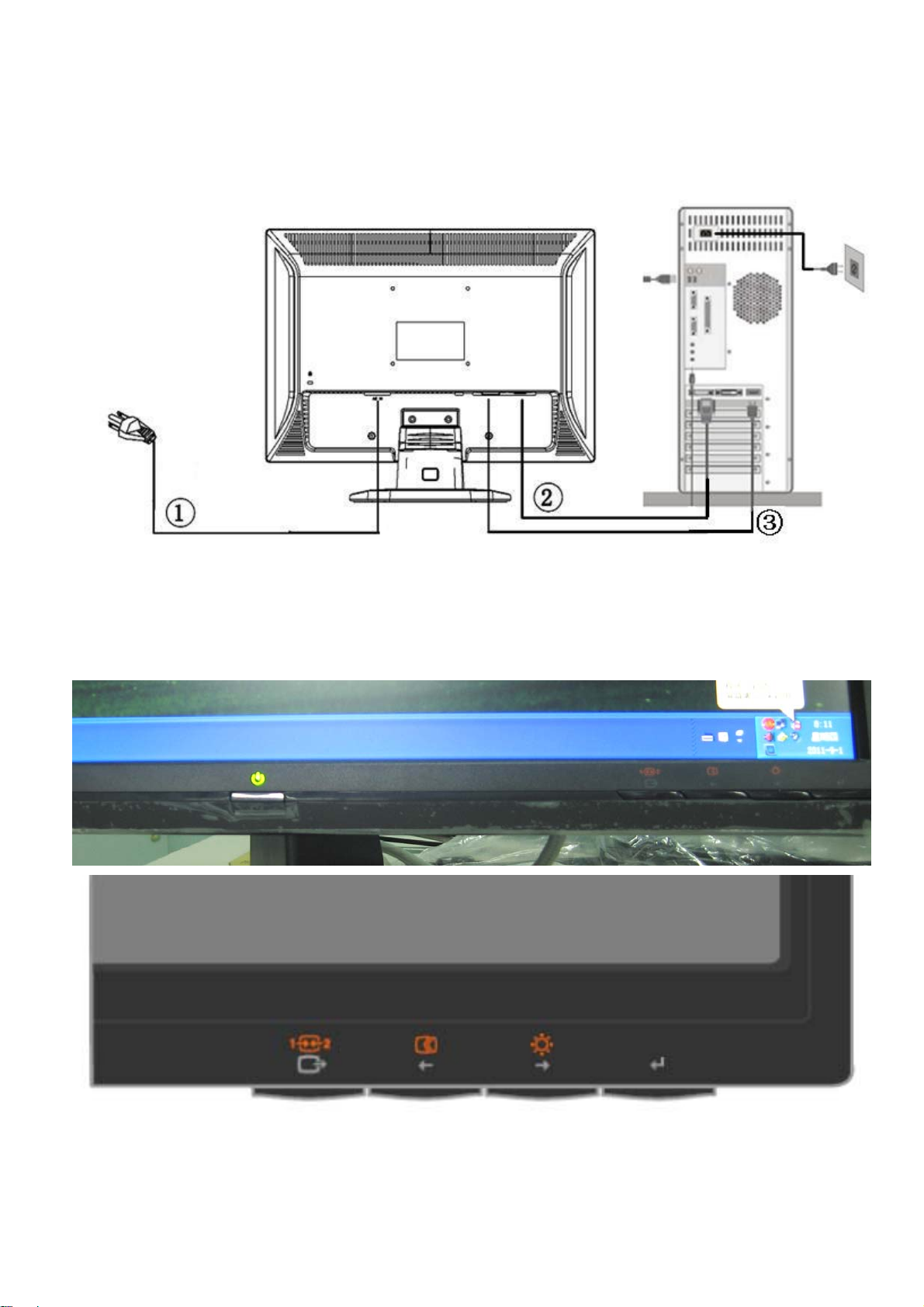
The power cord should be connected.
Connect the video cable from the video card of the PC to the monitor.
Press the power button to turn on the monitor, the power indicator will light up.
Press the power button to turn the monitor on or off.
The other control buttons are located at front panel of the monitor. By changing these settings, the picture can be
adjusted to your personal preferences.
2.2 Control Buttons
6
Lenovo Service Manual L2021W
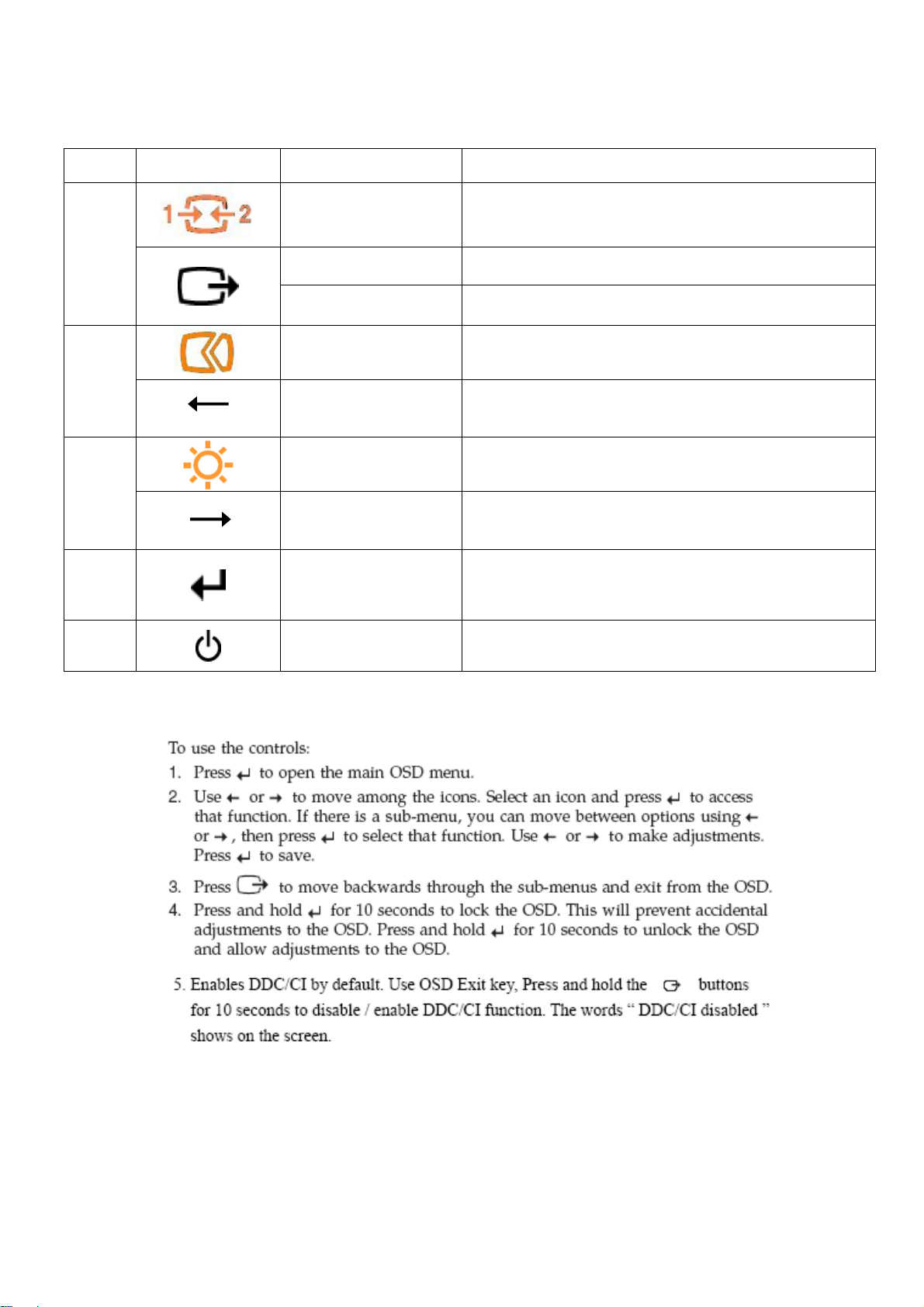
Icon Control Description
Input select Switches the video input source.DVI/D-SUB
1
DDC-CI
Pressed till 10 seconds, will enable/disable the DDC/CI.
2
3
4
5
Decrease - adjusting
Increase + adjusting
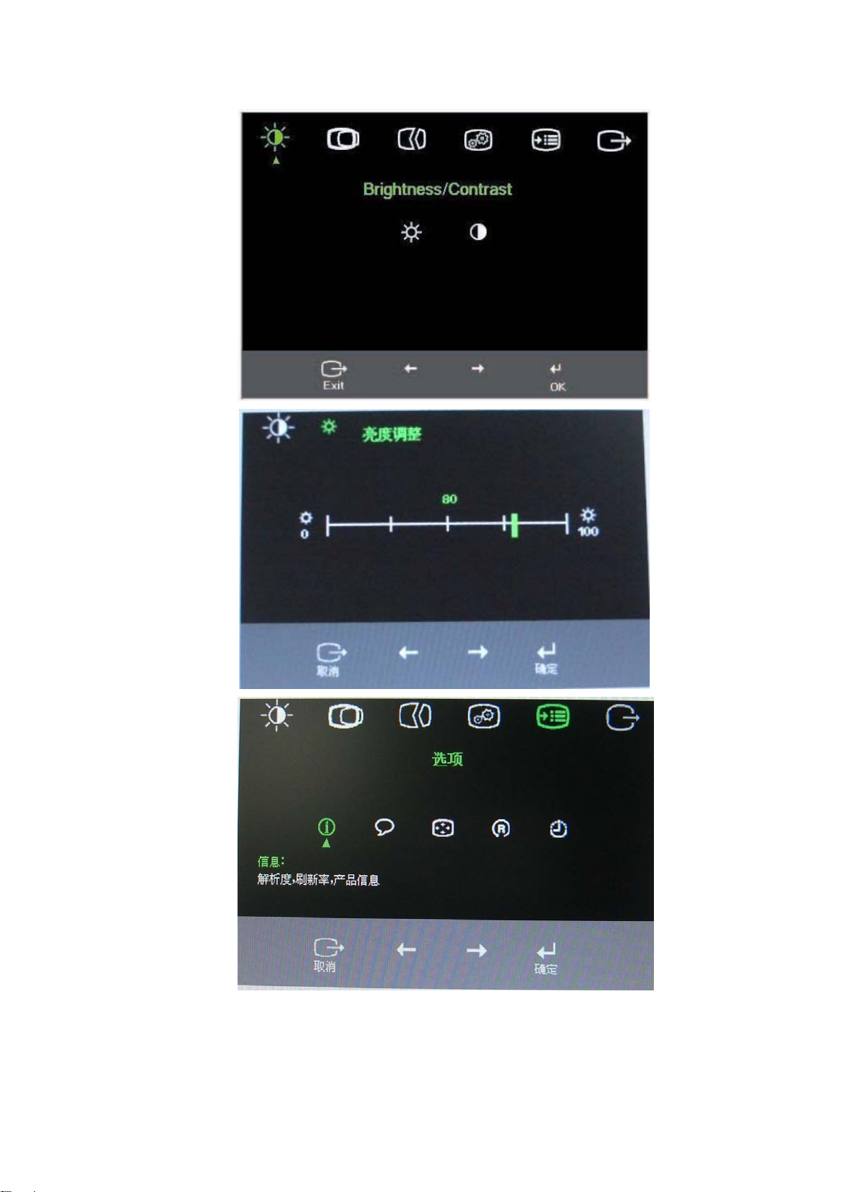
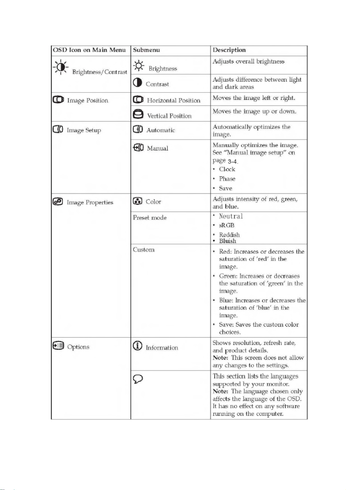
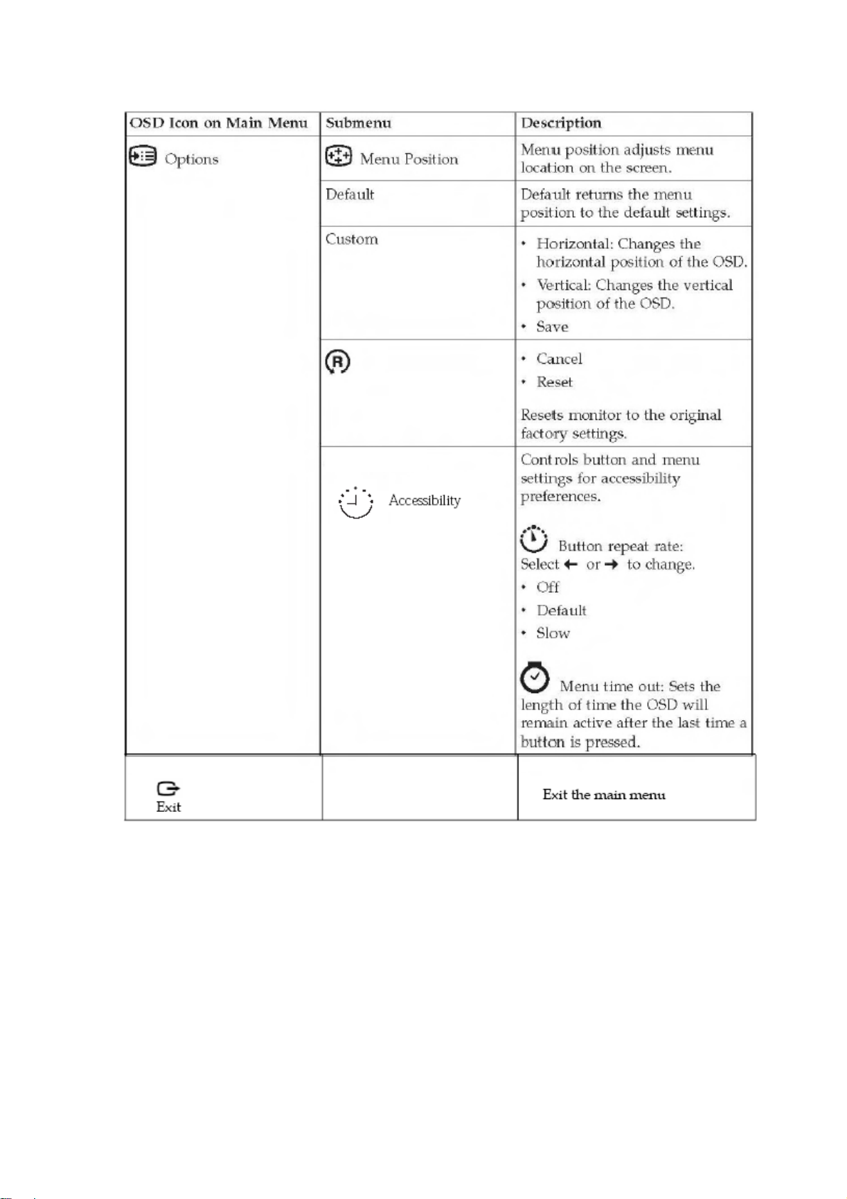
2.3 OSD User mode adjustment
a) OSD Menu adjustment steps:
Exit Exit current OSD return to last level.
Auto Press,Automatically adjust the image
OSD, it will decrease current value of bar, or move to last
item of menu.
Brightness If there is no any OSD,Direct access to Brightness.
OSD, it will increase current value of bar, or move to next
item of menu.
Active main menu while no OSD display,enter next level on
Menu
/Enter/OK
Power Button Power ON/OFF,and power indicator(Green and Amber).
main menu or sub menu status, or enter last level on
adjustment bar.Continued pressing 10 seconds will lock
menu or un-lock menu.
7
Lenovo Service Manual L2021W
8
Lenovo Service Manual L2021W
9
Lenovo Service Manual L2021W
10
Lenovo Service Manual L2021W
3.Interface description
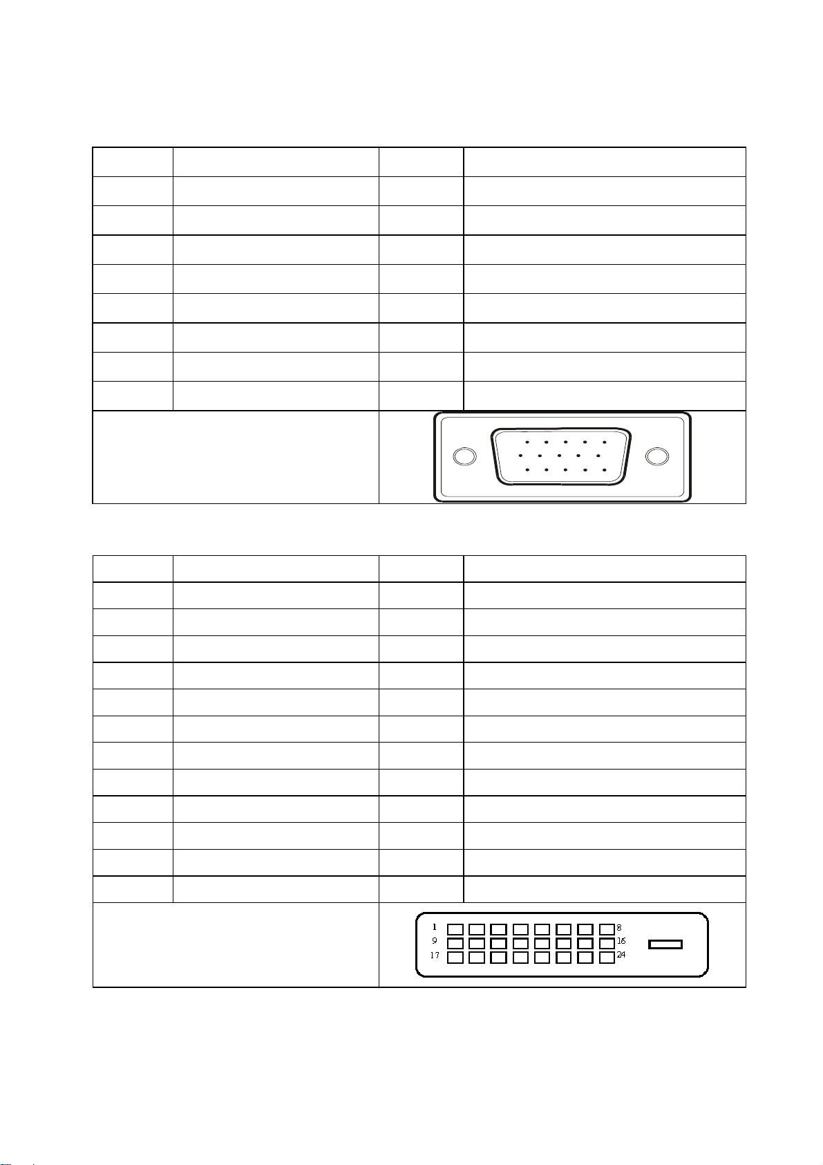
3.1 VGA Interface description
Pin No. Description Pin No. Description
1. Red Input 9. +5VDC
2. Green Input 10. GND
3. Blue Input 11. GND
4. GND 12. SDA- DDC-Serial Data
5. Connection detect 13. H Sync
6. Red GND 14. V Sync
7. Green GND 15. SCL- DDC-Serial Clock
8. Blue GND
15
VGA Connector layout
6
11 15
10
3.2 DVI Interface descrip ti on
Pin No. Description Pin No. Description
1. TMDS Data 2- 13. TMDS Data 3+
2. TMDS Data 2+ 14. +5V Power
3. TMDS Data 2/4 Shied 15. To detect signal cable connected
4. TMDS Data 4- 16. Hot Plug Detect
5. TMDS Data 4+ 17. TMDS Data 0+
6. DDC Clock 18. TMDS Data 0-
7. DDC Data 19. TMDS Data 0/5 Shield
8. Analog Vertical Sync 20. TMDS Data 5-
9. TMDS Data 1- 21. TMDS Data 5+
10. TMDS Data 1+ 22. TMDS Clock Shield
11. TMDS Data 1/3 Shield 23. TMDS Clock+
12. TMDS Data 3- 24. TMDS Clock-
DVI Connector layout
11
Lenovo Service Manual L2021W
4. Panel Feature
The Panel is a LTM200LT03-20.0 inch wide color TFT-LCD module . this module supports 1600×900 mode and
displays up to 16.7 millions colors.This model is composed of a TFT LCD panel,a driver circuit and a back light unit
(2CCFLs).
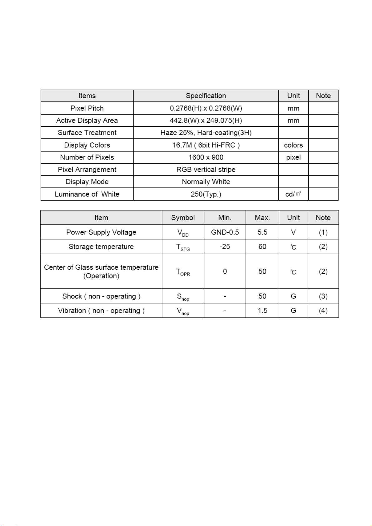
4.1 General Specifications
4.2 Absolute Maximum Ratings
12
Lenovo Service Manual L2021W
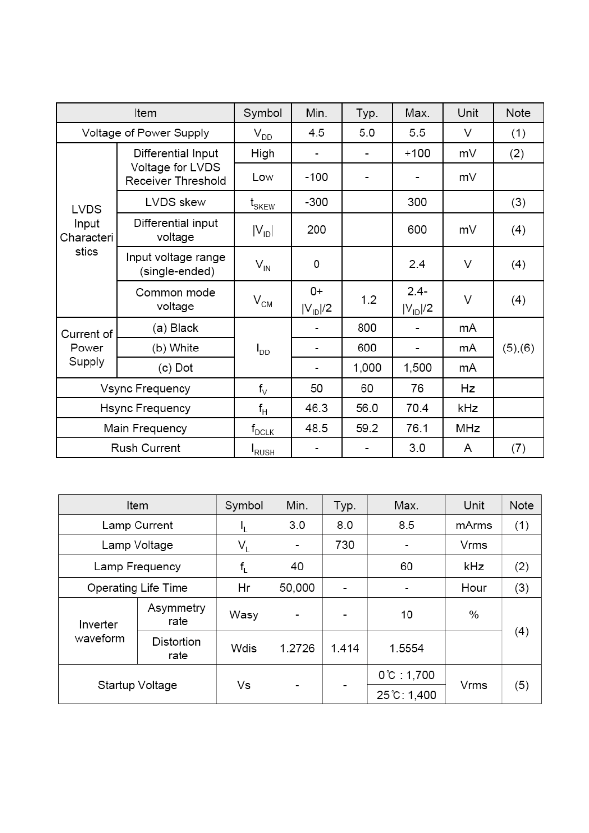
4.3 Electrical Characteristics
a) TFT LCD module
b) Backlight unit
13
Lenovo Service Manual L2021W
4.4 Panel Block Diagro am
4.5 LVDS Connector pin Assignment
14
Lenovo Service Manual L2021W
_
5.Block Diagram
5.1 LCD Block Diagram
LCD Block Diagram
AC supply
90V-264V
5.2 MainBoard Block Diagram
Main Board Block Diagram
DC-AC inverter
AC-DC
(5V/12V)
Power Board
Key board
Crystal24MHz
(X401)
2-CCFL backlight
Panel LVDS
Main Board
Computer VGA
Computer DVI
Input signal
LCD PANEL
(CN601/CN602)
SDA
SCL
FLASH ROM
M24C16
(U403)/NC
5V 3.3V 1.8V
Voltage converter
5V
RTD2122
(Include ADC, OSD, MCU)
(U401)
Key Board Control
(CN402)
DB15_SDA
DB15
SCL
D-Sub
Connector
(CN301)
DVI_SDA
DVI_SCL
Scalar IC RTD2525
Signal access
U501
H sync
V sync
DVI
Connector
(CN302)
15
Lenovo Service Manual L2021W
r
r
r
r
5.3 Power/ Inverter Board Block Diagram
Fuse EMI
AC input
100-240V
Power part
12V DC
IC Power Supply
Converter
Vcc
Switching MOS
Q802-AM9945
PWM Control IC
Rectifier
IC-PWM
IC901
IC801-TL494
Smoothing
Capacitor
C907
DC-AC
Transformer
T801
Open Lamp Protection
Transformer
T901
MOS
Q901
Sense
resisto
PhotoCoupler
Resonance NET
12V
Rectifie
5V
Rectifie
Vcc
Rectifie
regulating
Sampling
High Voltage
Output
2- CCFL
12V
5V
Inverter part
Current Sampling
16
Lenovo Service Manual L2021W
g
5.4 Software Flow Chart
Brightness
Contrast
Language
InputType
Start
Initial_MCU
Check if DataBuffer Is blank
Check if Sum is chan
Read parameter_from Buffer
ed ?
Init_GlobalVariables
Initial_MCU Device
while
Software Flow Chart
Y
To Write default values
InputTimingStableCounter
OsdCounter
PowerDownCounter
No signal message
UnsupportModeFlag
OSD Menu
PowerHandler
InputTiming
ModeHandler
MenuHandler
if factory mode?
DebugHandler
END
if standby mode?
N
LED turn-on
Show power on logo
InputTiming
Phaes/Frequency
Image setup
Color
Y
Enter factory mode OSD
------Just for your reference.
17
Lenovo Service Manual L2021W
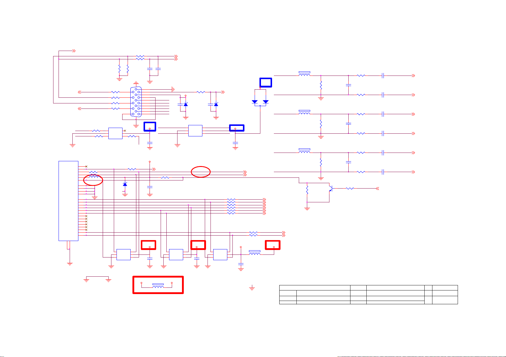
6. Circuit Schematic
6.1 Main Board---715G3327-1
input part---VGA/DVI/DDC
CN302
JACK
DDC1_SCL{4}
DSUB_V
DSUB_H
DDC1_SDA{4}
VSYNC
SYNC GND
DDC SCL
DDC SDA
1/3shield
2/4shield
0/5shield
clk shield
DAT0+
DAT0DAT1+
DAT1DAT2+
DAT2DAT3+
DAT3DAT4+
DAT4DAT5+
DAT5-
GND
26
25
DSUB_V {4}
H_Sync
V_Sy nc
DDC1-SCL
DDC1-SDA
VGA_G+
200R 1/10W 5%
VGA_R+
R330 200R 1/10W 5%
2007-02-06 add for EMI
150 OHM
8
15
FB304
R441100R 1/10W 5%
6
7
R440100R 1/10W 5%
14
+5V
16
HOT_PLUG
HPD
11
3
19
22
18
17
10
9
2
1
13
12
5
4
21
20
23
clk+
24
clk-
GND
R426 22R 1/10W 5%
R328 100R 1/10W 5%
R329 100R 1/10W 5%
R428 22R 1/10W 5%
R332
R304
2K2 1/16W
U103
1
I/O1
I/O4
2
GND
VDD
3 4
I/O2 I/O3
AZC199-04S
U107
AZC199-04S
1
I/O1
2
GND
3 4
I/O2 I/O3
R301 100R 1/16W
R303 100R 1/16W
R305
2K2 1/16W
CN301
10
5
15
9
4
14
8
3
13
7
2
12
6
1
11
DB15
17 16
R331
ESD_VC C
VGA_B+
ESD_VC C2
6
5
6
5
200R 1/10W 5%
R317 100R 1/ 16W
ZD306
NC
1 2
I/O4
VDD
C302
33pF
DVI_5V
C101
0.1uF/16V
C316
0.1uF/16V
C120
0.1uF/16V
C303
33pF
VGA_CON
DSUB_5V
VGA_B-
C414
VGA_B+
VGA_GVGA_G+
VGA_RVGA_R+
DDC1_SCL
DDC1_SDA
DVII_DETECT {4}
R316 10K 1/16W
U105
AZC199-04S
1
I/O1
2
GND
3 4
I/O2 I/O3
RTD_H {5}
RTD_V {5}
DSUB_5V
ZD304
RLZ5.6B
0.1uF/16V
1 2
U104
1
I/O1
2
GND
3 4
I/O2 I/O3
AZC199-04S
06' 11/23 del R328-R329
6
I/O4
5
VDD
R311
100R 1/16W
I/O4
VDD
ESD_VCC 1
C121
0.1uF/ 16V
C415
0.1uF/16V
6
5
1
2
3 4
ZD305
RLZ5.6B
1 2
H_Sync
V_Sy nc
U106
AZC199-04S
I/O1
GND
I/O2 I/O3
I/O4
VDD
DSUB_CONNECT
BAT54C
ESD_VCC
C112
0.1uF/16V
候綼
U103
DDC2_SCL
DDC2_SDA
R318 10R 1/16 W
R319 10R 1/16 W
R320 10R 1/16 W
R321 10R 1/16 W
R322 10R 1/16 W
R323 10R 1/16 W
ESD_VCC 1
6
5
MCU_VCC_S
1
2
{4}
D109
3
DDC2_SCL {4}
DDC2_SDA {4}
RX0P
RX0N
RX1P
RX1N
RX2P
RX2N
R324 10R 1/16W
R325 10R 1/16W
FB108
300 OHM
C119
0.1uF/16V
VGA_B+
VGA_B-
VGA_G+
VGA_G-
VGA_R+
VGA_R-
RX0P {5}
RX0N {5}
RX1P {5}
RX1N {5}
RX2P {5}
RX2N {5}
RXCP
RXCN
ESD_VCC
FB302
1 2
19R BEAD
FB301
1 2
19R BEAD
FB303
1 2
19R BEAD
RXCP {5}
RXCN {5}
R326
100K 1/16W 5%
R307
75R 1/10W 5%
R310
75R 1/10W 5%
R314
75R 1/10W 5%
Q301
MMBT390 4
R327
4K7 1/16W
R306 100R 1/16W
C305
5pF/50V
R308 100R 1/16W
R309 100R 1/16W
C308
5pF/50V
R312 100R 1/16W
R313 100R 1/16W
C310
5pF/50V
R315 100R 1/16W
C304
0.047uF
C306
0.047uF
C307
0.047uF
C309
0.047uF
C301
0.047uF
C311
0.047uF
HPD_CTL
RTD_B+
RTD_B-
RTD_G+
RTD_G-
RTD_R+
RTD_R-
RTD_B+ {5}
RTD_B- {5}
RTD_G+ {5}
RTD_G- {5}
RTD_R+ {5}
RTD_R- {5}
GND POWER
DGND
Power part---5V/3.3V/1.8V
ESD_VCC 2
FB109
300 OHM
ESD_VCC 1
18
T P V ( Top Victory Electronics Co . , Ltd. )
G3327-1-X-X-1-081 127
絬 隔 瓜 絪 腹
Key Component
Date
3.INPUT
Monday, Marc h 30, 2009
OEM MOD EL Size
BenQ G920HD
TPV MODEL
CBPCRRHBFQ1 1.2
PCB NAME
715G3327-1
Sheet
of
36
Rev
称爹
B
称爹
>
<
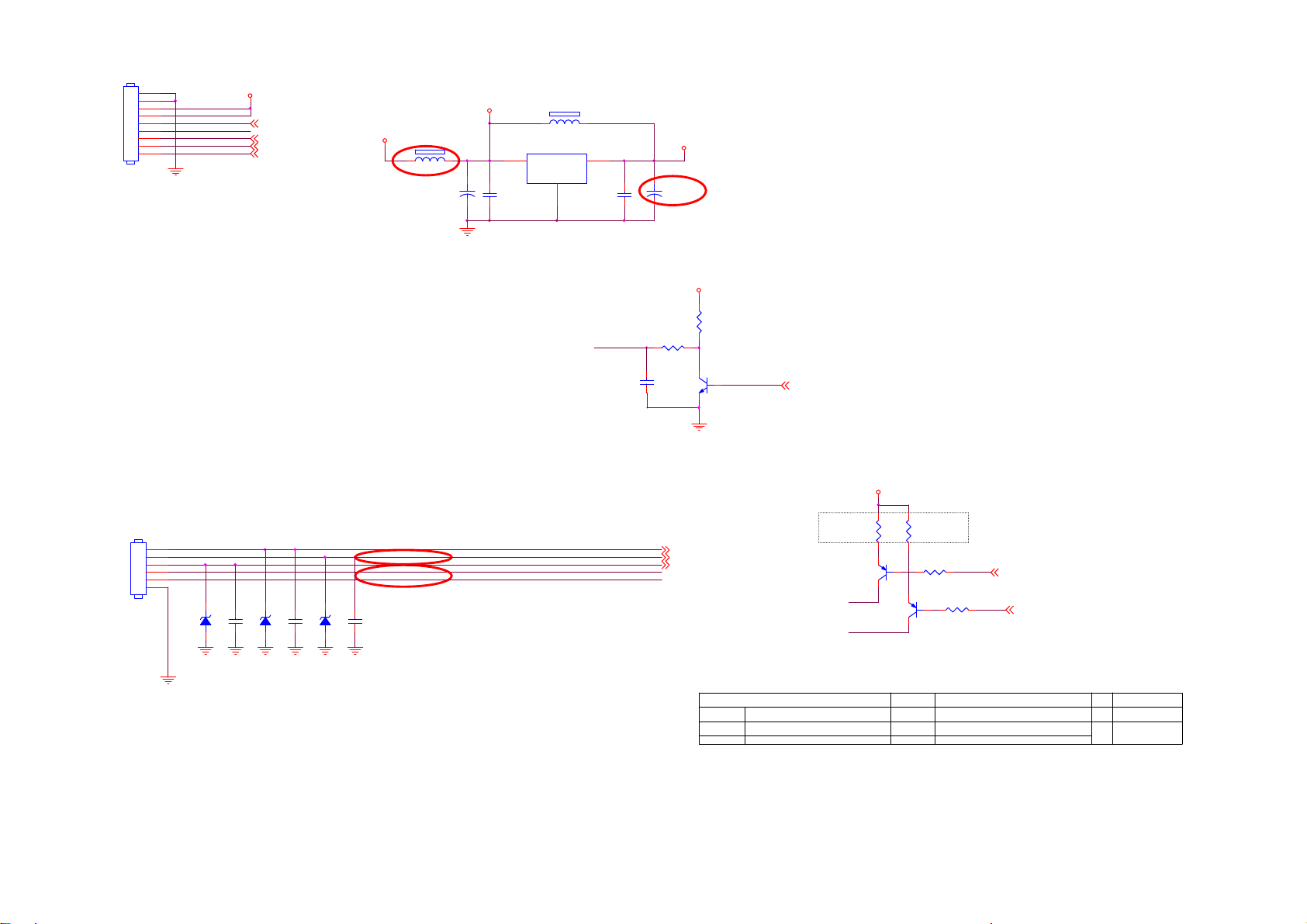
Lenovo Service Manual L2021W
CN201
CMVCC
DIM# {4}
PANEL_ID# {4}
Volume# {4}
Mute { 4}
Back light
Dimming(0.5V~3V)
Panel ID(0.5V~3V)
CMVCC
FB201
120Ω
C202
'07-01-10 change to Elite
MVC C
+
0.1uF/ 16V
C204
FB202
NC/120OHM
U201
AP1117E33LA
* BKLT-EN Hi g h ON (3. 3V)
23
VOUTVIN
VSS
1
BKLT-EN
C205
0.1uF/ 16V
VCC3
+
C203
'07-01-10 change to Elite
VCC3
R202
R201
200Ω 1/16W
C206
0.1uF/ 16V
4K7 1/16W
Q202
MMBT3904
INV_ON# {4}
VCC3
CONN
1
2
3
4
5
6
7
8
9
CMVCC
CMVCC
BKLT-VBRI
BKLT-EN
C_PANEL_INDEX
Volume#
Mut e
CN202
1
2
3
4
5
6
CONN
ZD202
C209
NC/UDZSNP5.6B
0.1uF/ 16V
1 2
C201
ZD203
0.1uF/ 16V
NC/UDZSNP5.6B
1 2
Near to Connect
MCU-RTD2122L/MCU_Vcc/DDC
'06-11-3 Remove R209(470 ohm)
C210
ZD201
0.1uF/ 16V
NC/UDZSNP5.6B
1 2
KEY0
KEY1
POWER_KEY #
LED_G
LED_R
KEY0 {4}
KEY1
POWER_KEY # {4}
19
{4}
T P V ( Top Victory Electronics Co . , Ltd. )
絬 隔 瓜 絪 腹
Key Component
Date
G3327-1-X-X-1-081127
2.POWER
Monday, March 30, 2009
R207
120R 1/16W
LED_R
LED_G
R208
120R 1/16W
Q204
123R210 10K 1/16W
MMBT3906
23
1
OEM MODEL Size
TPV MODEL
PCB NAME
Sheet
'06-12-29-3 Change R207,R208 Value
from 470ohm to 120ohm
LED_R# {4}
R213 10K 1/16W
Q205
MMBT3906
BenQ G920HD
CBPCRRHBFQ1 1.2
715G3327-1
26
of
LED_G# {4}
Rev
称爹
B
<
称爹
>
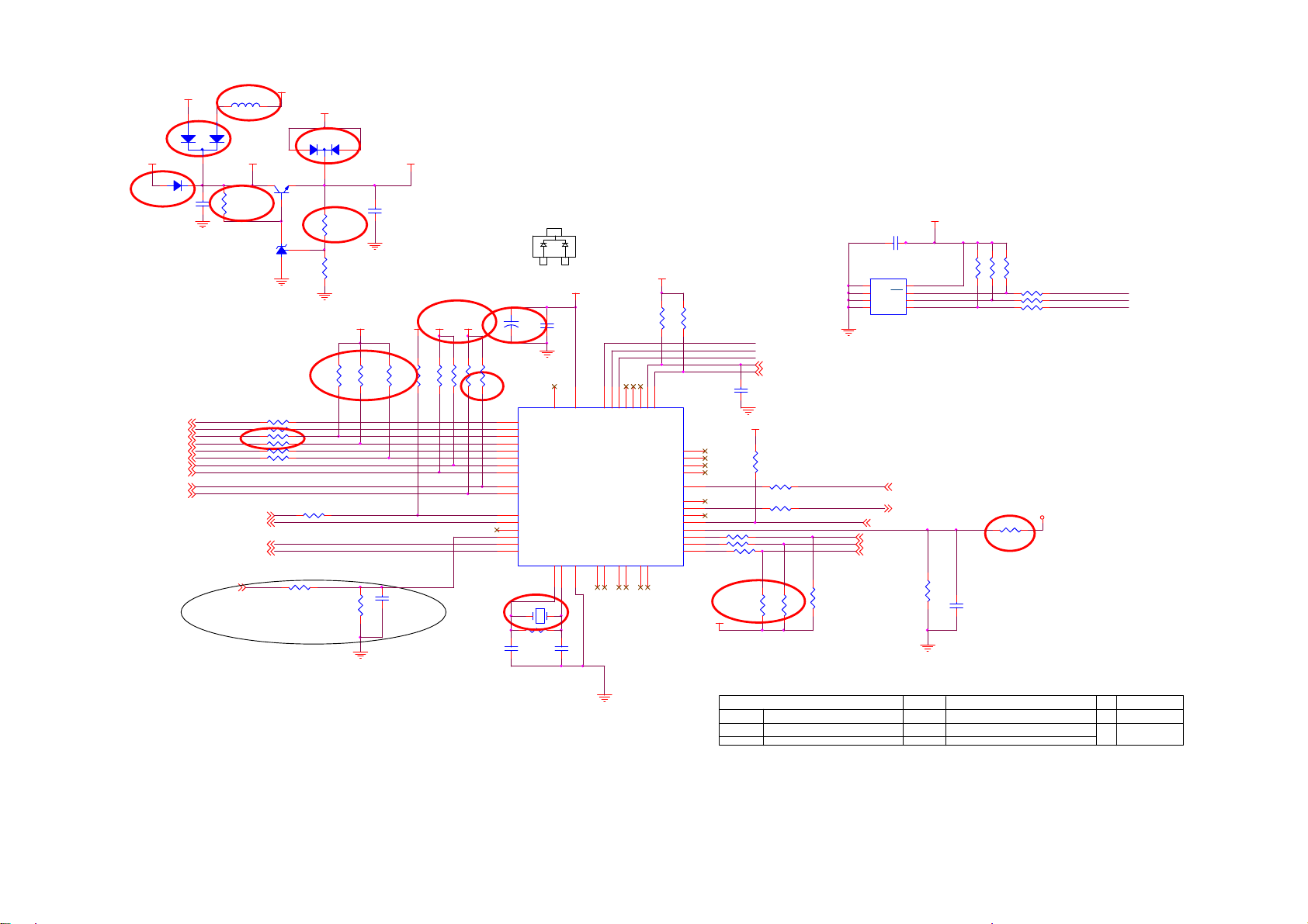
Lenovo Service Manual L2021W
CMVCC
'06-11-24
ADD D403
{3}
'06-11-24 D402 change
Value from BAT54 to
BAV70
DSUB_5V
D403
MCU_VCC_S
LL4148
C402
NC
'06-11-03
2006-11/7 Add pull high R451 to MVCC
,R453,R454 pull up MCU_VCC
2006-11/7 R423-R424 change from
100R to 1K
Volume#
Volume#{2}
Mut e
Mute{2}
PANEL_ID#{2}
PPWR_ON #{6}
DDC2_SCL{3}
DDC2_SDA
DDC1_SCL{3}
DDC1_SDA{3}
PANEL_ID#
DIM#
DIM#{2}
INV_ON#
INV_ON#{2}
DDC2_SCL
DDC2_SDA
DDC1_SCL
DDC1_SDA
{3}
PANEL_VCC
150 OHM
FB401
D402
BAV70
MCU_VCC_S
R402
1K 1/16W
U402
AZ431AN-AE1
R420 NC
R422 NC
R423 NC
R424 1K 1/16W
R430 100R 1/16WPPWR_ON#
R432 100R 1/16W
DVII _DETECT{3}
HPD_CTL
LED_G#{2}
LED_R#{2}
2007-01-11 ADD
DVI_5V
2007-02-06 add for EMI
CMVCC
D401 is Reserve for
D401
powerBoard CMVCC=3V
1
2
NC
3
Q401
MMBT39 04
R403
3.9KΩ 1/16W
'06-11-03
R404
10K 1/16W
R454
NC
R442 100R 1 /16W
LED_G#
LED_R# R435 100R 1/16W
R415
6K8 1/16W
R416
10K 1/16W 5 %
MCU_VCC
C412
1uF 10V
2006-11/23 change R413-4,R443-R444
pull high pin from DSUB_VCC ,DVI_VCC
to MCU_VCC
MCU_VCC_S
MCU_VCC_S
VCC3
R451
4K7 1/16W
C403
0.1uF/16V
R445 4K7 1/16W
R453
1K 1/16W
Closed to X'tal
MCU_VCC_S
R444 4K7 1/16W
R443 4K7 1/16W
3
1
2
BAT54C
MCU_VCC
C405
C406
+
10UF50V
0.1uF/ 16V
2007-1-15
change
from 4.7K
to 2.2K
44
45
46
47
48
10
11
12
13
14
4
414039383736353433
RST
P5.0/PWM0
P5.1/PWM1
P5.2/PWM2
P5.3/PWM3
P5.4/PWM4
1
P5.5/PWM5
2
DSCL2/P5.6
3
DSDA2/P5.7
5
ASCL1/P3. 0/RXD
8
ASDA1/P3.1/TXD
9
P3.2/INT0
P3.3/INT1
P3.4/T0
P3.5/T1
P7.6/CLKO2
P7.7
U401 RTD2122L-LF
24mhz
1 2
6K8 1/16W
VCC
RTD2122L
VSS
XO
XI
17
15
16
X40 1
R439
07-01-10 change to 93G22-45-H
C411
10pF
P1.0/T 2
NC
NC
6
7
2007-1/3 change ref from Y401
to X401
R4134K7 1/16W
'07-01-10
change to
Elite
R4144K7 1/16W
C401
10pF
MCU_VCC
R411
4K7 1/16W
P1.1
P1.2
P1.3
P1.4
P1.5
P6.6/CLKO1
NC
NC
NC
19
18
42
R412
4K7 1/16W
IICSDA
IICSCL
WP
RTD_SD3/SDI
RTD_SCLK
P1.6
P1.7
32
NC
31
NC
30
NC
29
NC
28
VSYNC
P6.7
P6.5
P6.4
P6.3/ADC3
P6.2/ADC2
P6.1/ADC1
P6.0/ADC0
NC
43
DSUB_V1
27
26
25
24
23
22
R433 100R 1/16W
21
R434 100R 1/16W
20
R437
MCU_VCC
2006-12-8 change R437,R401 from 10K to 3.9K
C409
NC/ 10pF
MCU_VCC
3.9K OHM +-1% 1/16W
RTD_SD3/SDI {5}
RTD_SCLK {5}
R425
10K 1/16W
R427 NC/1K 1/16W 5%
R429 0R05 1/16W
DSUB_CONNECT
POWER_KEY #
POWER_KEY #
KEY1
KEY0
R401
R438
3.9K OHM +-1% 1/16W
1
2
3
4 5
DSUB_V
CRYSTAR_OUT
DSUB_CONNECT {3}
POWER_KEY # {2}
KEY1 {2}
KEY0 {2}
3.9K OHM +-1% 1/16W
C404
NC
U403
NC
VCC
NC
WC
NC
SCL
VSS SDA
NC/M24C16
DSUB_V {3}
CRYSTAR_OUT {5}
10K 1/16W
R436
8
7
6
MCU_VCC
R406
R405
R407
NC/ 4K7 1/16W 5%
NC/ 4K7 1/16W 5%
4K7 1/16W 5%
R408 NC
R409 NC
R410 NC
MVC C
R431
6K8 1/16W
2006-11-3 change R431 from 1K to 6.8K
C410
0.1uF/16V
WP
IICSCL
IICSDA
Closed to MCU
T P V ( Top Victory Electronics Co . , Ltd. )
絬 隔 瓜 絪 腹
Key Component
Date
G3327-1-X-X-1-081127
4.MCU/RTD2122L
Monday, March 30, 2009
OEM MO DEL Size
BenQ G920HD
TPV MODEL
CBPCRRHBFQ1 1.2
715G3327-1
PCB NAME
Sheet
46
of
Rev
称爹
B
<
称爹
>
20
 Loading...