

Page 1

ZS1500
High Impedance Active Probe
Instruction Manual
February 2007
Page 2

Warranty
LeCroy warrants this oscilloscope accessory for normal use and operation within specification for a period of
one year from the date of shipment. Spare parts, replacement parts and repairs are warranted for 90 days.
In exercising its warranty, LeCroy, at its option, will either repair or replace any assembly returned within its
warranty period to the Customer Service Department or an authorized service center. However, this will be
done only if the product is determined by LeCroy’s examination to be defective due to workmanship or materials, and the defect is not caused by misuse, neglect, accident, abnormal conditions of operation, or damage
resulting from attempted repair or modifications by a non-authorized service facility.
The customer will be responsible for the transportation and insurance charges for the return of products to the
service facility. LeCroy will return all products under warranty with transportation charges prepaid.
This warranty replaces all other warranties, expressed or implied, including but not limited to any implied warranty of merchantability, fitness or adequacy for any particular purposes or use. LeCroy shall not be liable for
any special, incidental, or consequential damages, whether in contract or otherwise.
Corporate Headquarters
700 Chestnut Ridge Road
Chestnut Ridge, NY 10977-6499
Tel: (845) 578-6020, Fax: (845) 578-5985
Internet: www.lecroy.com
Copyright 2007 by LeCroy Corporation. All rights reserved.
LeCroy, ActiveDSO, JitterTrack, WavePro, WaveMaster, WaveSurfer, WaveLink, WaveExpert, WaveJet, and
Waverunner are registered trademarks of LeCroy Corporation. Other product or brand names are trademarks
or requested trademarks of their respective holders. Information in this publication supersedes all earlier versions. Specifications subject to change without notice.
LeCroy products are covered by International and U.S. patents, issued and pending.
Manufactured under an
ISO 9000 Registered
Quality Management System
Visit www.lecroy.com to view
the certificate.
ZS1500-OM-E Rev C
914907-00 Rev A
This electronic product is subject
to disposal and recycling regulations that vary by country and
region. Many countries prohibit the
disposal of waste electronic equipment in standard waste receptacles.
For more information about proper
disposal and recycling of your
LeCroy product, please visit
www.lecroy.com/recycle.
Page 3

DECLARATION OF CONFORMITY
according to ISO/IEC Guide 22 and EN 45014:1998
Manufacturer’s Name:
Manufacturer’s Address:
herewith declare that
Product(s) Name: Active Voltage Probe
Model Number(s): ZS1000, ZS1500
including all their options are in conformity with the provisions of the following EC directive(s), including
the latest amendments, and with national legislation implementing these directives:
and that conformity with Council Directive 73/23/EEC is based on
EN 61010-1:2001 Safety requirements for electrical equipment for measurement
control and laboratory use
and that conformity with Council Directive 89/336/EEC is based on
EN 61326/A3:2003 EMC requirements for electrical equipment for measurement
control and laboratory use
Emissions EN 55011/A2:2002 Conducted and Radiated Emissions
Immunity EN 61000-4-2/A2:2001 Electrostatic Discharge
LeCroy Corporation
700 Chestnut Ridge Road
Chestnut Ridge, NY 10977
USA
73/23/EEC Low Voltage Directive
89/336/EEC EMC Directive
EN 61000-4-3/A1:2003 RF Radiated Electromagnetic Field
By: David C. Graef European Contact:
Vice President & Chief Technology Officer Your local LeCroy Sales Office or
Place: LeCroy Corporation LeCroy Europe GmbH
700 Chestnut Ridge Road Waldhofer Str 104
Chestnut Ridge, NY 10977 D-69123 Heidelberg
USA Germany
Date: December 18, 2007 Tel: (49) 6221 82700
Fax: (49) 6221 834655
Warning: This is a Class A product. In a domestic environment this product may cause
radio interference, in which case the user may be required to take adequ ate measu res.
Page 4

BLANK PAGE
iv ZS1500-OM-E Rev C
Page 5

Contents
Table of Contents
Safety Information
Operator Safety ................................................................1-1
Conventions Used in this Manual .....................................1-1
Overview
Product Description ..........................................................2-1
Key Benefits ......................................................................2-1
Standard Accessories .......................................................2-2
Optional Accessories ........................................................2-2
Features and Accessories
Probe Head .......................................................................3-1
Description of Standard and Optional Accessories ..........3-1
A. Tips...........................................................................3-1
B. Grounds....................................................................3-3
C. Leads........................................................................3-6
Operation
Handling the Probe ...........................................................4-1
Connecting the Probe to the Test Instrument ...................4-1
Connecting the Probe to the Test Circuit ..........................4-1
Operation with a LeCroy Oscilloscope ..............................4-1
High Frequency Measurements
Input Loading ....................................................................5-1
Inductive Loading (Lead Length) ......................................5-1
Capacitive Loading ...........................................................5-2
Care and Maintenance
Cleaning ............................................................................6-1
Calibration Interval ............................................................6-1
Service Strategy ...............................................................6-1
Returning a Defective Probe .............................................6-1
Replacement Parts ...........................................................6-2
ZS1500-OM-E Rev C v
Page 6

ZS1500 High Impedance Active Probe
Performance Verification
Test Equipment Required .................................................7-1
Preliminary Procedure ......................................................7-2
Functional Check ..............................................................7-3
Procedure .........................................................................7-4
A. Output Zero Voltage .................................................7-4
B. Offset Accuracy ........................................................7-4
C. LF Attenuation Accuracy ..........................................7-7
Adjustment Procedure
Introduction .......................................................................8-1
Test Equipment Required .................................................8-1
Preliminary Procedure ......................................................8-2
Procedure .........................................................................8-3
A. Adjust Output Zero....................................................8-3
B. Adjust Offset Range..................................................8-4
C. Verify Calibration ......................................................8-6
Specifications
Nominal Characteristics ....................................................9-1
Warranted Characteristics ................................................9-1
Typical Characteristics ......................................................9-1
Environmental Characteristics ..........................................9-2
Physical Characteristics ....................................................9-2
Compliance and Certifications ..........................................9-3
Appendix A
Performance Verification Test Record ............................. A-1
Equipment Used: ............................................................. A-1
ZS1500 Test Record ........................................................ A-2
vi ZS1500-OM-E Rev C
Page 7

Safety Information
1 Safety Information
OPERATOR SAFETY
This symbol appears on the product:
This refers you to additional information contained in this manual. The
corresponding information in the manual is similarly denoted.
To avoid personal injury and to prevent fire or damage to the probe or
any products connected to it, review and comply with the following
safety precautions.
Connect to properly grounded instruments. This probe is to be only
used with test instruments with input connectors which the BNC shield
(ring) is connected to earth ground.
Connect the probe properly:
Connect the probe to the measurement instrument before connecting probe input to test circuit. Do not disconnect probe from
test instrument while the test leads are connected to a voltage
source.
Do not apply any potential to the input which exceeds the maximum ratings of the probe (section 9, "Specifications").
Comply with the voltage derating curve. When measuring high frequency signals, be sure to comply with the voltage versus frequency
derating curve (section 9, "Specifications").
Do not use in wet or explosive atmospheres.
For indoor use only. This probe is intended for indoor use and should
be operated in a clean, dry, environment.
Do not use the probe if any part is damaged. All maintenance should
be referred to qualified service personnel.
Avoid physical injury. The probe tips are extremely sharp. Use care
when handling to prevent injury, including accidental skin puncture.
ZS1500-OM-E Rev C 1–1
Page 8

ZS1500 High Impedance Active Probe
Use of the probe and or the test instrument it is connected to in a manner not specified by the manufacturer may impair the protection mechanisms.
CONVENTIONS USED IN THIS MANUAL
The following conventions may appear in this manual:
Note
A Note contains information relating to the use of the product.
CAUTION
A Caution contains information that should be followed to avoid possible
damage to the probe or the products connected to it.
This symbol appears on the product:
This refers you to additional information contained in this manual. The
corresponding information in the manual is similarly denoted.
###
1–2 ZS1500-OM-E Rev C
Page 9

Overview
2 Overview
PRODUCT DESCRIPTION
The 1.5 GHz ZS1500 is a small, high impedance active probe designed
to meet today’s increasing demand for measurements on a variety of
test points.
With low input capacitance and high input resistance, circuit loading is
minimized.
The ZS1500 can be used with LeCroy’s WaveSurfer, WaveRunner,
WaveMaster, and WavePro series platforms with firmware version 4.9.3
or later.
With the ProBus interface, the ZS1500 becomes an integral part of the
oscilloscope. The probe can be controlled from the oscilloscope’s front
panel. The oscilloscope provides power to the probe, so there is no
need for a separate power supply or batteries.
KEY BENEFITS
• High frequency performance
• Low input capacitance
• Wide dynamic range
• ProBus interface
• Four interchangeable tips for probing a variety of test points (one
standard, three optional accessories)
ZS1500-OM-E Rev C 2–1
Page 10

ZS1500 High Impedance Active Probe
STANDARD ACCESSORIES
The ZS1500 probe is shipped with the following standard accessories:
Item: Quantity:
Straight Tip 4
Sprung Hook 2
Right Angle Connector 1
Offset Ground 2
Ground Blade 1
Copper Pad 2
Short Single lead 1
Long Single Lead 1
Instruction Manual 1
Certificate of calibration 1
Y-lead Adapter 1
Color Coding Rings 4 sets
OPTIONAL ACCESSORIES
The following items are available as optional accessories for the
ZS1500 probe:
IC Lead Tip
Discrete SMD Tip
Bent Sharp Tip
Bendable Pogo Ground
Ground Spring with Hook
Solder-in Ground
Square Pin Ground Spring
Short Right-angle Lead
Long Right-angle Lead
For part number information for standard and optional accessories refer
to, Care and Maintenance, Replaceable Parts List.
###
2–2 ZS1500-OM-E Rev C
Page 11
Features and Accessories
3 Features and Accessories
The ZS1500 probe is provided with numerous features and accessories
to make probing and connecting to different test points easier than ever.
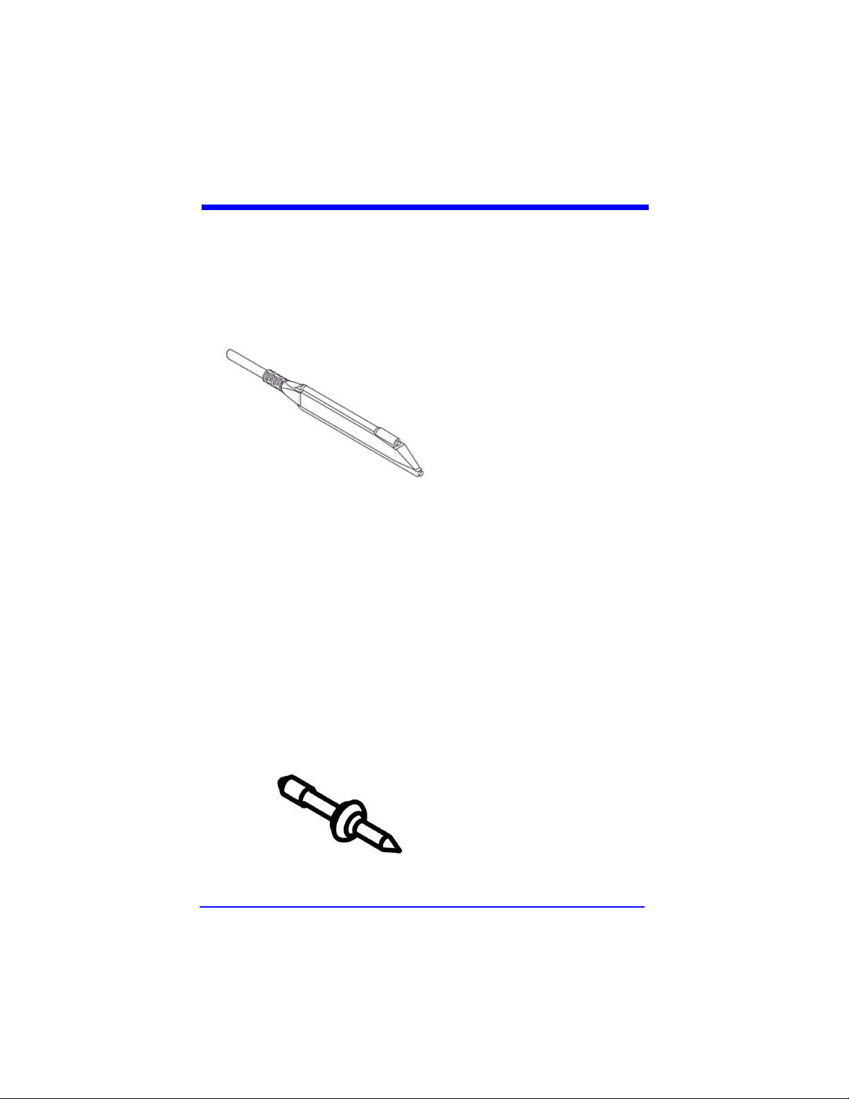
PROBE HEAD
The small, low mass probe
head is designed for ease of
use and high performance.
The probe tip socket fits easily onto 0.025 inch square
pins for direct access to test
points. Several different
adapters are available which
connect directly in the probe
socket.
The ground socket will accept
several different ground leads
to provide a short ground
path for high frequency performance.
DESCRIPTION OF STANDARD AND OPTIONAL ACCESSORIES
The following accessories can be pushed into the probe tip socket,
ground socket or any other socketed lead or adapter.
A. Tips
Straight Tip
Rugged tip designed to connect to the smallest vias and
small test points. Fits in
either probe socket.
PK-ZS-001, package of 4
ZS1500-OM-E Rev C 3–1
Page 12

ZS1500 High Impedance Active Probe
IC Lead Tip
Covered in insulation on all
sides (except for a small
edge), this tip was designed
to prevent shorting neighboring IC leads. The gold part of
the tip is not insulated and
should touch the IC lead to be
tested. It is one-size-fits-all
and will work with any IC lead
pitch. Fits in either probe
socket.
The IC Lead Tip is an
optional accessory for the
ZS1500.
PACC-PT003, package of 4
Discrete SMD Tip
The crescent shape of this tip
is designed to fit tightly on
capacitors, resistors, transistors and other surface mount
components with discrete
leads. Fits in either probe
socket.
The SMD Discrete Tip is an
optional accessory for the
ZS1500.
PACC-PT004, package of 4
3–2 ZS1500-OM-E Rev C
Page 13

Features and Accessories
Bent Sharp Tip
B. Grounds
Micro Clip (0.5 mm) Sprung Hook
Made out of titanium, this tip
is ideal for situations that
require the user to hold the
probe parallel to the circuit
board under test. Also gives
the user more control when
holding the probe like a pencil. Fits in either probe socket.
The Bent Sharp Tip is an
optional accessory for the
ZS1500.
PACC-PT005, package of 4
A pincher-like spring hook tip
designed to hold onto fine
pitch leads and small components, commonly found in
SMD ICs. Fits in either probe
socket, or can be used with a
lead.
The Sprung Hook is a standard accessory for the
ZS1500 and available in
black and red.
PK-ZS-007R, PK-ZS-007B,
package of 4 each
ZS1500-OM-E Rev C 3–3
Page 14

ZS1500 High Impedance Active Probe
Ground Spring with Hook
A flexible spring connected to
a square pin that fits into
either of the probe head
sockets. Designed to be used
as a ground lead, there is a
hook on the end of the spring
so that it can probe general
circuits.
The Ground Spring with
Hook is an optional accessory for the ZS1500.
PACC-LD001, package of 4
Square Pin Ground Spring
A flexible spring connected to
a square pin that fits into
either of the probe sockets.
Designed to be attached to a
square pin on the circuit
under test.
The square pin ground spring
is an optional accessory for
the ZS1500 probe.
PACC-LD002, package of 4
3–4 ZS1500-OM-E Rev C
Page 15
Features and Accessories
Offset Ground
The offset pin is designed to
be attached to either socket
of the probe head. The offset
pin is the highest quality
grounding solution and is recommended in high frequency
applications.
The offset ground is designed to connect to the ground socket and
wrap around the probe head. This gives the ability to a probe signal
and ground that are extremely close together. The short length provides high-quality grounding for high-frequency applications.
PK-ZS-002, package of 4
Ground Blade and Copper Pad
The Ground Blade and
Copper Pad are intended to
work together for the best
grounding solution for probing an IC. The Ground
Blade is designed to provide a short, low inductance ground path. The
Copper Pad is adhesive
backed to stick to the top of
an IC, and can then be soldered to the IC ground.
The Copper Pad can also
be used with the Offset
Ground.
PK-ZS-008, package of 4
PK-ZS-009, package of 4
ZS1500-OM-E Rev C 3–5
Page 16

ZS1500 High Impedance Active Probe
C. Leads
While longer leads provide greater flexibility when connecting the probe
to a circuit, the added inductance may degrade the fidelity of high frequency signals. See Section 4 for additional information.
Short and Long Lead
This lead has a socket on one
end and a square pin on the
other to connect to the input
or ground socket of the probe
body, and may be used for
general purpose probing.
PK-ZS-003 (short),
PK-ZS-004 (long), packages
of 4
Y Lead Adapter
This lead is used for both
ground and input lead
simultaneously.
It has two sockets on one
end and two square pins on
the other and may be used
for general purpose probing.
PK-ZS-005, packages of 4
###
3–6 ZS1500-OM-E Rev C
Page 17

Operation
4 Operation
HANDLING THE PROBE
Exercise care when handling and storing the probe. Always handle the
probe by the probe body or compensation box. Avoid putting excessive
strain or exposing the probe cable to sharp bends.
CONNECTING THE PROBE TO THE TEST INSTRUMENT
The ZS1500 probe has been designed for use with LeCroy’s
WaveSurfer, WaveRunner, WaveMaster, and WavePro platforms
equipped with the ProBus interface. When you attach the probe output
connector to the oscilloscope’s input connector, the oscilloscope will
recognize the probe, provide proper termination and activate the probe
control functions in the user interface.
CONNECTING THE PROBE TO THE TEST CIRCUIT
To maintain the high performance capability of the probe in
measurement applications, care must be exercised in connecting the
probe to the test circuit. Increasing the parasitic capacitance or
inductance in the input paths may introduce a “ring” or slow the rise time
of fast signals. Input leads which form a large loop area will pick up any
radiated electromagnetic field which passes through the loop and may
induce noise into the probe input.
Using one of the available accessories makes the ZS1500 probe with its
small profile and low mass head ideally suited for applications in dense
circuitry.
OPERATION WITH A LECROY OSCILLOSCOPE
When the ZS1500 probe is connected to any compatible LeCroy
oscilloscope, the displayed scale factor and measurement values will be
automatically adjusted.
Control through the oscilloscope’s interface can be found in the
Coupling menu of the channel to which the probe is connected.
Turning the Volts/Div knob will control the oscilloscope’s scale factor to
give full available dynamic range up to 2 V/div.
###
ZS1500-OM-E Rev C 4–1
Page 18

ZS1500 High Impedance Active Probe
BLANK PAGE
4–2 ZS1500-OM-E Rev C
Page 19

High Frequency Measurements
5 High Frequency Measurements
INPUT LOADING
When you touch a probe to the circuit under test, the probe will affect
your measurement because of the probe’s input impedance introduced
into the circuit. All probes present resistive, capacitive and inductive
loading.
INDUCTIVE LOADING (LEAD LENGTH)
A significant element in this circuit is the inductance shown in the input
ground leads of the oscilloscope probe.
Figure 5-1. Probe Input Equivalent Circuit
The ground lead is the primary return path for the current resulting from
the input voltage acting on the probe’s input impedance. The ground
lead and input lead inductances act with the probe’s input capacitance
to form series L-C network. The impedance of a series LC network will
drop dramatically at its resonant frequency. This is the cause of the
"ring" we often see after the leading edge of pulses in measured waveforms. This effect is referred to as ground lead corruption. Because it is
impossible to eliminate either the L or C from this circuit, the method to
improve waveform fidelity is to raise the resonant frequency beyond the
bandwidth of interest in the measurement.
The resonant frequency of a simple LC circuit can be represented by:
1
F
Resonance
ZS1500-OM-E Rev C 5–1
------------------
=
2π LC
Page 20

ZS1500 High Impedance Active Probe
The resonant frequency of a series LC circuit can be raised by decreasing the inductance, capacitance or both.
Since the input capacitance is already very low and cannot be reduced,
you can only try to reduce the inductance. This can be accomplished by
using the shortest possible input lead as well as the shortest possible
ground lead.
For example, to obtain the shortest possible ground lead when measuring IC related signals, attach a small piece of copper clad material to the
top of the IC package and connect this to the package grounding wires.
Using the shortest ground lead and input lead available makes probing
signals on the package easier and makes for the shortest lead length for
the best signal fidelity.
To illustrate how dramatic this effect is, we will work a simple example.
Assuming an input capacitance of 0.9 pF and a total lead length (input
and ground) of 2 inches (inductance of ≈ 25 nH/inch) such a setup may
cause ringing with a resonant frequency (f
) of:
0
-------------------------------------------------------------------
f
0
2π 50 10
This frequency is well within the passband of the probe and will therefore show up as part of the measured signal at faster time/div settings.
To determine how fast a waveform to be measured can be without causing ringing on a probe like this, divide the BW (ringing frequency) of the
probe into 0.35:
0.35
t
rise
Any input signal with a rise time faster than 0.47 ns can cause ringing.
CAPACITIVE LOADING
Capacitive loading is usually the most troublesome of the three loading
effects.
It can affect the rise time, bandwidth and delay time measurements.
5–2 ZS1500-OM-E Rev C
---------BW
1
9–
0.9 10
0.35
---------------------
750MHz
750 MHz==
12–
×××
0.47 ns== =
Page 21

High Frequency Measurements
At higher frequencies the capacitive loading can affect the amplitude as
well as the waveshape of the measured signal by introducing an exponential response to the waveform.
For a simple RC network the time constant of this exponential response
is:
t
rise
where C
combined circuit and probe resistance.
For a setup where C
measured rise time will be 0.495 ns, which will correspond to a band-
width of 909 MHz, assuming no inductive loads.
(parallel combination of 250 Ω and 1 MΩ is still 250 Ω)
To illustrate the effect of capacitive loading at higher frequencies:
At a frequency of 750 MHz the reactance of the 0.9 pF capacitance is
236 Ω, and at 1.0 GHz the reactance has been lowered to 177 Ω
is the combined probe and circuit capacitance and R
total
= 0.9 pF and a source resistance is 250 Ω, the
t
(t
=2.2 x 0.9 X 10
rise
250 Ω
Source
V
Figure 5-2. Probe input equivalent circuit
2.2 C
× R
-12
x 250 Ω = 0.495 ns)
Input inductance
×=
total
0.9 pF 1 MΩ
total
total
is
If, at a given frequency, the source impedance is large with respect to
the input impedance, a measurable reduction in the output signal amplitude may occur.
Z
probe
V
out
ZS1500-OM-E Rev C 5–3
--------------------------------------
Z
+
probeZsource
Vin×=
Page 22

ZS1500 High Impedance Active Probe
where:
Z
is the probe’s input impedance and
probe
Z
As an example:
At 750 MHz, where the probe input impedance has reduced to 236 Ω,
and a source resistance of 250 Ω the probe output amplitude is reduced
to:
is the source impedance
source
V
out
236
-----------------------236 250+
###
0.49 Vin×==
5–4 ZS1500-OM-E Rev C
Page 23

Care and Maintenance
6 Care and Maintenance
CLEANING
The exterior of the probe and cable should be cleaned only using a soft
cloth lightly moistened with water or isopropyl alcohol. The use of abrasive agents, strong detergents, or other solvents may damage the
probe. Always ensure that the input leads are free of debris.
Note
The probe case is not sealed and should never be immersed in any
fluid.
CALIBRATION INTERVAL
The recommended calibration interval is one year. (Performance Verification and Adjustment Procedures are included in this manual.)
SERVICE STRATEGY
The ZS1500 probe utilizes fine pitch surface mount devices. It is therefore impractical to attempt to repair in the field. Defective probes must
be returned to a LeCroy service facility for diagnosis and exchange. A
defective probe under warranty will be replaced with a factory refurbished probe. A probe that is not under warranty can be exchanged for
a factory refurbished probe for a modest fee. You must return the defective probe in order to receive credit for the probe core.
RETURNING A DEFECTIVE PROBE
The procedure for returning a defective probe is as follows:
Contact your local LeCroy sales representative to find out where to
return the product. All returned products should be identified by model
number and serial number. Provide your name and contact number and
if possible describe the defect or failure. In case of products returned to
the factory, a Return Authorization Number (RAN) should be used. The
RAN can be established by contacting your nearest LeCroy office, or the
New York Customer Care Center.
Return shipment should be made prepaid. LeCroy cannot accept COD
or Collect Return shipments. We recommend air-freighting. It is impor-
ZS1500-OM-E Rev C 6–1
Page 24

ZS1500 High Impedance Active Probe
tant that the RAN be clearly shown on the outside of the shipping package for prompt redirection to the appropriate department.
1. Contact your local LeCroy sales or service representative to obtain
a Return Authorization Number.
2. Remove all accessories from the probe. Do not include the manual.
3. Pack the probe in its case, surrounded by the original packing material (or equivalent) and box.
4. Label the case with a tag containing
• The RAN
• Name and address of the owner
• Probe model and serial number
• Description of failure
5. Package the probe case in a cardboard shipping box with adequate
padding to avoid damage in transit.
6. Mark the outside of the box with the shipping address given to you
by the LeCroy representative; be sure to add the following:
• ATTN: <RAN assigned by the LeCroy representative>
• FRAGILE
7. Insure the item for the replacement cost of the probe.
8. Ship the package to the appropriate address.
REPLACEMENT PARTS
The probe connection accessories and other common parts can be
ordered through the regional customer care centers. Refer to list below
for LeCroy part numbers. Defective probes can be replaced on an
exchange basis. The replacement exchange probe will have been factory repaired, inspected and calibrated to the same standards as a new
product. In order to obtain an exchange probe, you must return the
defective probe. The returned probe should be sent back to the regional
customer care center without any accessories, manual or case.
6–2 ZS1500-OM-E Rev C
Page 25

Care and Maintenance
Figure 6-1. Replaceable Parts Selected by Input and Ground Accessory
ZS1500-OM-E Rev C 6–3
Page 26

ZS1500 High Impedance Active Probe
Table 6-1: Replaceable Parts List
Item LeCroy P/N Replacement
Straight Tip PK-ZS-001 4
Offset Ground PK-ZS-002 4
Short Lead PK-ZS-003 4
Long Lead PK-ZS-004 4
Y Lead Adapter PK-ZS-005 4
Right Angle Connector PK-ZS-006 4
Sprung Hook - Red PK-ZS-007R 4
Sprung Hook - Black PK-ZS-007B 4
Ground Blade PK-ZS-008 4
Copper Pad PK-ZS-009 4
Color Coding Rings PK-ZS-010 4 sets
Quantity
IC Lead Tip PACC-PT003 4
Discrete SMD Tip PACC-PT004 4
Bent Sharp Tip PACC-PT005 4
Solder-In Ground PACC-CD007 2
Bendable Pogo Ground PACC-CD008 2
Ground Spring with Hook PACC-LD001 4
Square Pin Ground Spring PACC-LD002 4
Short Right Angle Lead PACC-LD003 4
Long Right Angle Lead PACC-LD004 4
###
6–4 ZS1500-OM-E Rev C
Page 27

Performance Verification
7 Performance Verification
This procedure can be used to verify the warranted characteristics of
the ZS1500 High Frequency Probe.
The recommended calibration interval for the model ZS1500 is one
year. The complete performance verification procedure should be performed as the first step of annual calibration. Test results can be
recorded on a photocopy of the Test Record provided in Appendix A at
the end of the manual.
Performance verification can be completed without removing the probe
covers or exposing the user to hazardous voltages. Adjustment should
only be attempted if a parameter measured in the Performance Verification Procedure is outside the specification limits.
Note
Adjustment should only be performed by qualified personnel.
This procedure tests the following specifications:
• Output Zero Voltage
• Offset Accuracy
• LF Attenuation Accuracy
TEST EQUIPMENT REQUIRED
Table 7-1 lists the test equipment and accessories (or their equivalents)
that are required for performance verification of the ZS1500 Probe.
This procedure has been developed to minimize the number of calibrated test instruments required.
Only the parameters listed in boldface in the "Minimum requirements"
column must be calibrated to the accuracy indicated.
Because the input and output connectors types may vary on different
brands and models of test instruments, additional adapters or cables
may be required.
ZS1500-OM-E Rev C 7–1
Page 28

ZS1500 High Impedance Active Probe
Table 7-1. List of Required Equipment
Description Minimum Requirements Test Equipment Examples
Digital Oscilloscope ProBus interface; Windows-
Digital Multimeter (DMM)
with test probe leads
Function Generator Sine Wave output amplitude
Power Supply 0-12 V, settable to 10 mV HP E3611A
BNC Coaxial Cable (2 ea.) Male to Male, 50 Ω, 36" Cable Pomona 2249-C-36 or
BNC Tee Connector Male to Dual Female Pomona 3285
Calibration Fixture ProBus Extender Cable LeCroy PROBUS-CF01
Terminator, Precision, BNC 50 Ω ± 0.05% LeCroy TERM-CF01
Banana Plug Adapter (2 ea.) Female BNC to Dual Banana
BNC to Mini-grabber BNC Male to Mini-grabber Cable,
based
4.5 digit
DC: 0.1% Accuracy
AC: 0.1% accuracy
adjustable to 14.14 V
into 1 MΩ at 70 Hz
Plug
36"
p-p
(5 V
LeCroy WaveRunner Xi,
WaveSurfer Xs
Agilent Technologies 34401A or
Fluke 8842A-09
Agilent Technologies 33120A or
)
Stanford Research Model DS340
rms
Pomona 5697-36
Pomona 1269
Pomona 5187-C-36
PRELIMINARY PROCEDURE
1. Connect the ZS1500 probe to the female end of the ProBus Extension Cable. Connect the male end of the ProBus Extension Cable to
channel 1 of the oscilloscope.
2. Turn the oscilloscope on and allow at least 30 minutes warm-up time
for the ZS1500 and test equipment before performing the Verification Procedure.
3. Turn on the other test equipment and allow these to warm up for the
time recommended by the manufacturer.
4. While the instruments are reaching operating temperature, make a
photocopy of the Performance Verification Test Record (located in
Appendix A), and fill in the necessary data.
5. Select the channel to which the probe is connected. Set the oscilloscope scale factor to 20 mV/div.
7–2 ZS1500-OM-E Rev C
Page 29

Performance Verification
6. Disconnect the ProBus Extender Cable from the oscilloscope. Verify
that the scale factor changes from 20 mV/div to 2 mV/div.
7. Re-connect the ProBus extender Cable to the oscilloscope.
The warranted characteristics of the ZS1500 are valid at any temperature within the Environmental Characteristics listed in the Specifications.
However, some of the other test equipment used to verify the performance may have environmental limitations required to meet the accuracy needed for the procedure. Make sure that the ambient conditions
meet the requirements of all the test instruments used in his procedure.
Note
The correct operation of the ZS1500 controls requires software version
5.0.0.2 or higher. The software version in the test oscilloscope can be
verified by selecting Utilities, Utilities Setup... from the menu bar, then
the Status tab.
Contact your local LeCroy representative or visit www.lecroy.com if the
software in your oscilloscope requires updating.
FUNCTIONAL CHECK
The functional check will verify the basic operation of the probe functions.
It is recommended that the Functional Check be performed prior to the
Performance Verification Procedure.
1. Return to the factory default settings by:
a. Selecting File, Recall Setup... from the menu bar.
b. Then touching the Recall Default button.
2. Touch the C1 trace label to open the C1 Vertical Adjust dialog.
3. Verify that the probe sensed (ZS1500) is displayed as a dialog tab.
ZS1500-OM-E Rev C 7–3
Page 30
ZS1500 High Impedance Active Probe
PROCEDURE
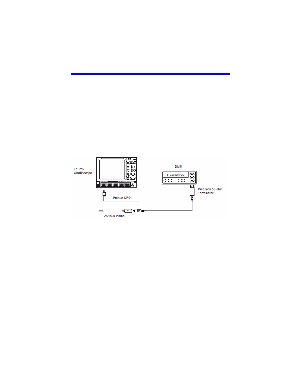
A. Output Zero Voltage
1. Connect one end of a BNC cable to the female BNC connector on
the probe end of the ProBus extender cable. Connect the precision
50 Ω terminator to the other end of the BNC cable.
2. Connect the banana plugs of the Precision terminator to the input of
the DMM. Make sure that the plug corresponding to the BNC shield
(marked "Ground") is connected to the LO or COMMON input of the
DMM. Refer to Figure 7-1 for setup information.
Figure 7-1. Output Zero Voltage Test Setup
3. Set the OFFSET on the oscilloscope to zero.
4. Set the DMM to read DC Volt on the most sensitive range.
5. Record the voltage measured on the DMM to 10 µV resolution as
"Output Zero Voltage" in the Test record.
6. Check that the voltage indicated by the DMM is between ±800 µV.
7. Disconnect the DMM from the precision 50 Ω terminator. Leave the
remaining setup in place for the next step.
B. Offset Accuracy
1. Connect the BNC end of the BNC to mini-grabber cable to a female
end of the BNC tee adapter and connect a female BNC to dual
7–4 ZS1500-OM-E Rev C
Page 31
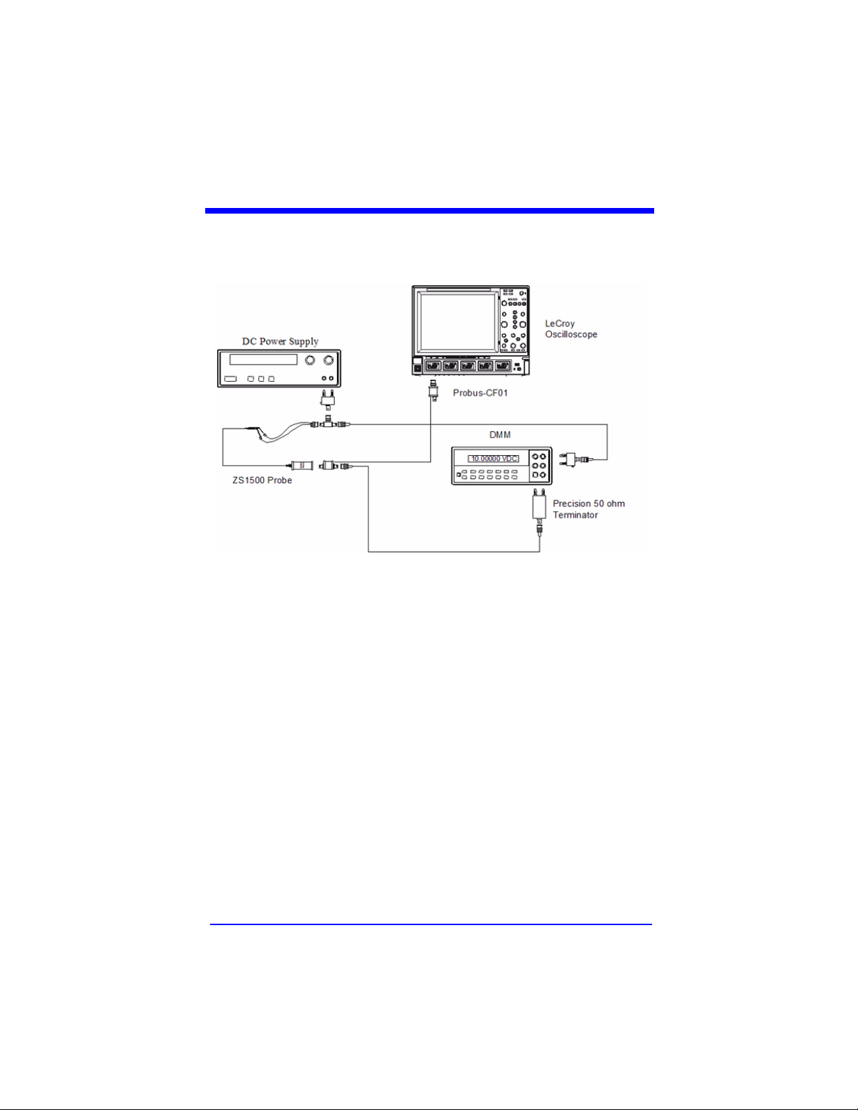
Performance Verification
banana plug adapter to the male end of the BNC tee. (Refer to Figure 7-2).
Figure 7-2. Offset and LF Attenuation Accuracy Test Setup
2. Carefully insert the Straight Tips (supplied in accessory kit) into the
sockets of the probe head. Attach the red lead of the mini-grabber to
the signal input and the black lead to the ground input of the probe
head.
3. Set the power supply to approximately 0 Volt.
4. Plug the dual banana plug adapter with probe attached into the output terminals of the power supply with ground side of the adapter
(and the ground side of the probe head) connected to the positive
terminal of the power supply.
5. Attach a BNC cable to the unused female port of the BNC tee and a
dual banana plug adapter to the other end of the cable and plug the
dual banana plug adapter into the DMM input. Make sure the side of
the banana plug adapter corresponding to the BNC shield (marked
"GROUND") is connected to the LOW or COMMON input of the
DMM.
6. Adjust the power supply to an output of 10.0 V ± 100 mV as indi-
ZS1500-OM-E Rev C 7–5
Page 32

ZS1500 High Impedance Active Probe
cated on the DMM.
7. Record the DMM reading, which should be a negative number, to
10 mV resolution as "Power Supply Negative Output Voltage" in the
Test Record.
8. Add 10 (to correct for the +10 V offset as described in step B-13) to
the "PS Negative Output Voltage" recorded in step B-7. (Do NOT
adjust the power supply output amplitude).
9. Divide the resulting sum by 10.
10. Record the answer to three significant places as "Expected Negative
Output Voltage" in the test record.
11. Remove the banana plug adapter, connected to the power supply,
from the DMM and connect the precision 50 Ω terminator to the
DMM, making sure that the banana plug side marked "GROUND" is
connected to the LOW or COMMON input of the DMM.
12. Set the DMM to read DC Volt on the most sensitive range.
13. Verify that the display for channel 1 is turned ON. Turn the oscilloscope OFFSET knob to read +10.00 V on the oscilloscope display.
14. After the DMM has settled, record the reading to 100 µV resolution
as "Measured Negative Output Voltage" in the Test Record.
15. Subtract the measured voltage as recorded in step B-14 from the
expected output voltage recorded in step B-10. Be sure to include
the sign of each of the values in the calculation.
16. Record the answer to three significant places as "Offset Error Voltage" in the Test Record.
17. Verify that the error is between ±10.8 mV.
Note:
The error term is derived from the Offset Accuracy specification of ±1%
±8 mV. Using a 10.0 V offset setting, the maximum error would be 108
mV referred to the input, which becomes ±10.8 mV error referred to the
÷
output (taking into account the
18. Using the oscilloscope’s OFFSET knob, set the probe offset to 0 V,
as indicated in the on-screen display.
7–6 ZS1500-OM-E Rev C
10 attenuation).
Page 33

Performance Verification
19. Remove the dual banana plug adapter with the ZS1500 attached
from the power supply and reconnect to the supply but now with the
grounded side of the banana plug (and grounded socket of the
probe head) connected to the negative terminal of the power supply
output.
20. Disconnect the DMM from the precision 50 Ω terminator and connect the DMM to the dual banana plug adapter connected to the
power supply output.
21. Record the DMM reading, which should be a positive number, to 10
mV resolution as "Power Supply Positive Output Voltage" in the Test
Record.
22. Subtract 10 from the output voltage recorded in step B-21. Divide
this number by 10.
23. Record the result to three significant places as "Expected Positive
Output Voltage" in the Test Record.
24. Set the oscilloscope OFFSET to –10.00 V as read on the oscilloscope display.
25. Remove the banana plug adapter from the DMM and connect the
precision 50 Ω terminator to the DMM, making sure that the banana
plug side marked "GROUND" is connected to the LOW or COM-
MON input of the DMM.
26. Record the DMM reading to three significant places as "Measured
Positive Output Voltage" in the Test Record.
27. Subtract the Measured Output Voltage as recorded in step B-26
from the Expected Output Voltage recorded in step B-23. Be sure to
include the sign of the values in the calculation.
28. Record the result to 100 µV resolution as "Offset Error Voltage" in
the Test Record.
29. Verify that the output error is between ±10.8 mV.
30. Return the oscilloscope offset to 0 Volt. Leave the setup connections for the next step.
C. LF Attenuation Accuracy
1. Disconnect the BNC tee at the power supply from the dual banana
plug adapter. Connect the BNC tee to the output of the function gen-
ZS1500-OM-E Rev C 7–7
Page 34

ZS1500 High Impedance Active Probe
erator. (Use a 50 Ω termination if the function generator requires
such a load.) Refer to Figure 7-3.
Figure 7-3. LF Attenuation Accuracy setup
2. Disconnect the DMM from the precision 50 Ω terminator and con-
nect the DMM to the dual banana plug adapter connected to the
function generator output.
3. Set the DMM to read AC Volt and set the range to measure 5.0
Vrms.
4. Set the mode of the function generator to sine wave, the frequency
to 70 Hz and the output amplitude to 5 Vrms ±10 mV as measured
on the DMM.
5. Record the output voltage to 1 mV resolution as "Generator Output
Voltage" in the Test Record. Be careful not to alter the output amplitude after the reading is recorded.
6. Divide the reading recorded in step C-5 by 10 and record the result
with 100 µV resolution as "Expected Output Voltage, top range" in
the Test Record.
7. Remove the banana plug adapter, connected to the function generator, from the DMM and connect the precision 50 Ω terminator to the
DMM, making sure that the banana plug side marked "GROUND" is
7–8 ZS1500-OM-E Rev C
Page 35

Performance Verification
connected to the LOW or COMMON input of the DMM.
8. After the DMM reading has stabilized, record the reading to 100 µV
resolution as "Measured Output Voltage, top range" in the Test
Record.
9. Calculate the error by dividing the measured output voltage
recorded in step C-8 by the expected top output voltage recorded in
step C-6. Subtract 1 from this ratio and multiply by 100% to get the
error in percent.
Measured Output Voltage
⎛⎞
Error
10. Record the calculated error to two decimal places (±0.xx%) as "Gain
Error, top range" in the test record.
11. Verify that the error is less than ±1.0 %.
12. Disconnect the precision 50 Ω terminator from the DMM.
13. Connect the banana plug adapter connected via a BNC cable to the
BNC tee at the function generator to the DMM. Verify that the side of
the plug marked "Ground" is connected to the LOW or COMMON
input of the DMM.
--------------------------------------------------------------
=
⎝⎠
Expected Output Voltage
1–
100%
×
14. Adjust the sine wave generator output amplitude to approximately
2.5 Vrms as measured on the DMM.
15. Record the reading to 1 mV resolution as "Generator Output Voltage, mid range" in the Test Record. Be careful not to alter the output
amplitude after the reading is recorded.
16. Divide the reading recorded in step C-15 by 10.
17. Record the result to 100 µV resolution as "Expected Output Voltage,
mid range" in the test record.
18. Remove the banana plug adapter from the DMM and connect the
precision 50 Ω terminator to the DMM, making sure that the banana
plug side marked "GROUND" is connected to the LOW or COM-
MON input of the DMM.
ZS1500-OM-E Rev C 7–9
Page 36

ZS1500 High Impedance Active Probe
19. After the DMM has stabilized, record the reading to 100 µV resolu-
tion as "Measured Output Voltage, mid range" in the Test record.
20. Calculate the error by dividing the measured output voltage
recorded in step C-19 by the expected top output voltage recorded
in step C-17. Subtract 1 from this ratio and multiply by 100% to get
the error in percent.
Measured Output Voltage
⎛⎞
Error
21. Record the calculated error to two decimal places (±0.xx %) as
"Gain Error, mid range" in the Test record.
22. Verify that the mid range gain error is less than ±1.0%
This completes the Performance Verification of the ZS1500. Complete
and file the Test Record, as required to support your internal calibration
procedure.
--------------------------------------------------------------
=
⎝⎠
Expected Output Voltage
1–
100%
×
Apply suitable calibration label to the ZS1500 housing as required.
###
7–10 ZS1500-OM-E Rev C
Page 37

Adjustment Procedure
8 Adjustment Procedure
INTRODUCTION
You can use this procedure to adjust the ZS1500 probe to meet the warranted specifications. This procedure should only be performed if the
probe fails to meet the Performance verification tests for Output Zero or
Offset Accuracy.
Gain which affects LF attenuation accuracy cannot be adjusted during
routine calibration. Probes which fail LF frequency accuracy during performance verification must be returned to the factory for rework.
If the probe cannot be adjusted to meet the Performance verification limits, repair may be necessary.
To assure probe accuracy, check the calibration of the ZS1500 every
1000 hours or once a year if used infrequently. Before calibration, thoroughly clean and inspect the probe as outlined in the Care and Maintenance section.
To assure the probe will meet the published specifications over the
entire temperature range, adjustment must be performed in a controlled
ambient environment with temperature of 23 °C ±5 °C.
Caution
The adjustment procedure will require removal of the probe control circuit cover. This cover is part of the ESD protection system of the
ZS1500. To protect the probe, you should perform the entire procedure
on a static dissipating work surface. Wear an antistatic wrist strap and
follow standard static control procedures.
TEST EQUIPMENT REQUIRED
Table 8-1 lists the test equipment and accessories (or their equivalents)
that are required for complete calibration of the ZS1500 Probe. Specifications given for the test equipment are the minimum necessary for
accurate calibration. All test equipment is assumed to be correctly calibrated and operating within the specification listed. Detailed operating
ZS1500-OM-E Rev C 8–1
Page 38

ZS1500 High Impedance Active Probe
instructions for the test equipment are not given in this procedure. Refer
to the test equipment manual if more information is needed
If alternate test equipment is substituted, control settings or calibration
equipment setups may need to be altered.
Table 8-1. List of Required Equipment
Description Minimum Requirements Test Equipment
Examples
Digital Oscilloscope ProBus interface; Windows-
based
Digital Multimeter
(DMM) with test probe
leads
Power Supply 0-12 V, settable to 10 mV HP E3611A
BNC Coaxial Cable (2
ea.)
BNC Tee Connector Male to Dual Female Pomona 3285
Calibration Fixture ProBus Extender Cable LeCroy PROBUS-CF01
Terminator, Precision, BNC
Banana Plug Adapter
(2 ea.)
BNC to Mini-grabber BNC Male to Mini-grabber
4.5 digit
DC: 0.1% Accuracy
AC: 0.1% accuracy
Male to Male, 50 Ω, 36"
Cable
50 Ω ±0.05% LeCroy TERM-CF01
Female BNC to Dual Banana
Plug
Cable, 36"
LeCroy WaveRunner Xi or
WaveSurfer Xs
Agilent Technologies
34401A or
Fluke 8842A-09
Pomona 2249-C-36 or
Pomona 5697-36
Pomona 1269
Pomona 5187-C-36
PRELIMINARY PROCEDURE
1. Remove the two screws that secure the plastic cover on the cable
end of the ProBus interface housing.
2. Gently pull on the probe cable to slide the circuit board assembly
from the metal housing.
3. Connect the ZS1500 probe to the female end of the ProBus extension cable, being careful to line up all six pins of the probe connector. Connect the male end of the ProBus extension cable to channel
1 of the oscilloscope.
8–2 ZS1500-OM-E Rev C
Page 39

Adjustment Procedure
4. Apply power to the oscilloscope and test equipment.
5. Allow at least 30 minutes warm-up time for the ZS1500 and test
equipment before starting the calibration procedure.
PROCEDURE
A. Adjust Output Zero Voltage
1. Connect one end of a BNC cable to the probe end of the ProBus
extension cable. Connect the Precision 50 Ω Terminator to the other
end of the BNC cable.
2. Connect the banana plugs of the precision 50 Ω terminator to the
input of the DMM. Make sure the plug corresponding to the BNC
shield (marked ’Ground’) is connected to the LO or COMMON input
of the DMM. Refer to Figure 8-1 for setup information.
Figure 8-1. Output Zero Voltage Adjustment Setup
3. Select the channel to which the probe and ProBus extender is connected. Set OFFSET on the oscilloscope to zero as indicated on the
on-screen display.
4. Set the DMM to read DC Volt on the most sensitive range.
5. Verify that the probe inputs are not connected to any signal.
6. Adjust OFFSET ZERO on the board until the DMM reads
0 V ±100 µV. Refer to Figure 8-2 for adjustment location.
ZS1500-OM-E Rev C 8–3
Page 40

ZS1500 High Impedance Active Probe
7. Leave the setup connections in place for the next step.
OFFSET RANGE
OUTPUT ZERO
Figure 8-2. Adjustment Locations
B. Adjust Offset Range
1. Connect the BNC end of the BNC to mini-grabber cable to a female
end of the BNC tee adapter and a female BNC to dual banana plug
adapter to the male end of the BNC tee.
2. Carefully insert Straight Tips (supplied in the accessory kit) into the
ZS1500 probe head sockets. Attach the red lead of the mini-grabber
to the signal input and the black lead to the ground input of the
probe.
3. Set the power supply for approximately 0 Volt.
4. Plug the dual banana plug adapter, with the probe attached, into the
output terminal of the power supply. Make sure the side of the
banana plug corresponding to the probe ground and BNC ground is
connected to the negative terminal of the power supply.
5. Attach a BNC cable to the unused female port of the BNC tee and a
dual banana plug adapter to the other end of the BNC cable and
plug this into the DMM. Make sure the side of the banana plug corresponding to the BNC shield (marked ’GROUND’) is connected to the
LO or COMMON input of the DMM. Refer to Figure 8-3 for setup
information.
6. Using the DMM to monitor the voltage, adjust the power supply to an
output of 10.00 V ±10 mV. Record the reading.
8–4 ZS1500-OM-E Rev C
Page 41

Adjustment Procedure
Figure 8-3. Offset Range Adjustment setup
7. Remove the banana plug adapter from the DMM connect the precision 50 Ω terminator into the DMM Input. Make sure the side of the
banana plug corresponding to the BNC shield (marked ’GROUND’)
is connected to the LO or COMMON input of the DMM.
8. Verify that the display for channel 1 is turned on. Set the oscilloscope OFFSET knob to –10.00 V. as read on the oscilloscope
screen.
9. Set the DMM to read DC Volt on the most sensitive range.
10. Subtract 10.0 V from the power supply output voltage recorded in
step B-7. Be sure to keep track of the sign of the result.
11. A d j u s t OFFSET RANGE until the DMM reads the same voltage ±1
mV as calculated in step B-11. Be sure the sign agrees.
12. Repeat steps A-3 through A-7 of the Adjust Offset Zero procedure.
13. Disconnect the probe from the ProBus extender and re-install the
circuit board into the probe case, being careful to align the ProBus
interface connector with the opening on the other end of the case.
ZS1500-OM-E Rev C 8–5
Page 42

ZS1500 High Impedance Active Probe
C. Verify Calibration
Repeat the Performance Verification procedure to ensure compliance
with the warranted specifications.
Apply a calibration sticker, if required, in accordance with your quality
control procedures.
###
8–6 ZS1500-OM-E Rev C
Page 43

Specifications
9 Specifications
NOMINAL CHARACTERISTICS
Nominal characteristics describe parameters and attributes that are
guaranteed by design, but do not have associated tolerances.
Input Dynamic range ±8 V
Offset Range ±12 V
Maximum Input Voltage 20 V
Intended Output Load 50 Ω
Attenuation ÷10
Output Connector ProBus
Interface ProBus
Oscilloscope Full Compatibility LeCroy oscilloscope with firmware ver-
1
Subject to input voltage vs. frequency derating. See Figure 9-1.
1
sion 5.0.0.2 or later
WARRANTED CHARACTERISTICS
Warranted characteristics are parameters with guaranteed performance. Unless otherwise noted, tests are provided in the Performance
Verification Procedure for all warranted specifications.
Low Frequency Attenuation
Accuracy ±0.50% plus uncertainty of 50 Ω termi-
nation
Output Zero ±2 mV, referred to the input
TYPICAL CHARACTERISTICS
Typical characteristics are parameters with no guaranteed performance.
Tests for typical characteristics are not provided in the Performance
Verification Procedure.
Bandwidth (Probe only) 1.5 GHz
ZS1500-OM-E Rev C 9–1
Page 44

ZS1500 High Impedance Active Probe
Input Capacitance 0.9 pF
DC Input Resistance 1 MΩ
ENVIRONMENTAL CHARACTERISTICS
Temperature, warranted 15 to 35 °C
Temperature, operating 0 °C to 50 °C
Temperature, non-operating -40 °C to 71 °C
Relative Humidity 80% max. up to 31 °C, decreasing lin-
early to 45% max. at 50 °C
Altitude up to 2000 m
PHYSICAL CHARACTERISTICS
Probe Head Size:
Length 61 mm (2.4 in.)
Width 7.3 mm (0.29 in.)
Height 13.1 mm (0.52 in.)
Cable Length 1.3 m (51.1 in.)
Weight:
Probe only 100 g (3.5 oz.)
Shipping 0.85 kg (1.87 lbs.)
Input Sockets Signal and ground sockets are com-
patible with 0.635 mm (0.025 in)
square pins, and 0.91 mm (0.036 in)
maximum diameter round pins
9–2 ZS1500-OM-E Rev C
Page 45

Input Voltage vs. Fre quency
100
10
1
Voltage [V] AC pk
0.1
1 10 100 1000 10000
Frequency [MHz]
Figure 9-1. Input Voltage vs. Frequency
COMPLIANCE AND CERTIFICATIONS
Specifications
CE Declaration of Conformity
Low Voltage Directive: EN 61010-2-031:2002
Safety requirements for electrical
equipment for measurement control
and laboratory use.
Part 031: Particular requirements for
hand-held probe assemblies for electrical measurement and test.
E M C D i r ec t i v e : E N 61 3 2 6 / A 3 :2 0 0 3
EMC requirements for electrical equipment for measurement control and
laboratory use.
ZS1500-OM-E Rev C 9–3
Page 46
ZS1500 High Impedance Active Probe
Electromagnetic Emissions: EN 55011/A2:2002 Class A Radiated
Emissions.
Electromagnetic Immunity: EN 61000-4-2/A2:2001 Electrostatic
Discharge.
(Air/Contact Discharge: 4 kV)
EN 61000-4-3/A1:2003
RF Radiated Electromagnetic Field
(80 MHz to 1 GHz; 3 V/m)
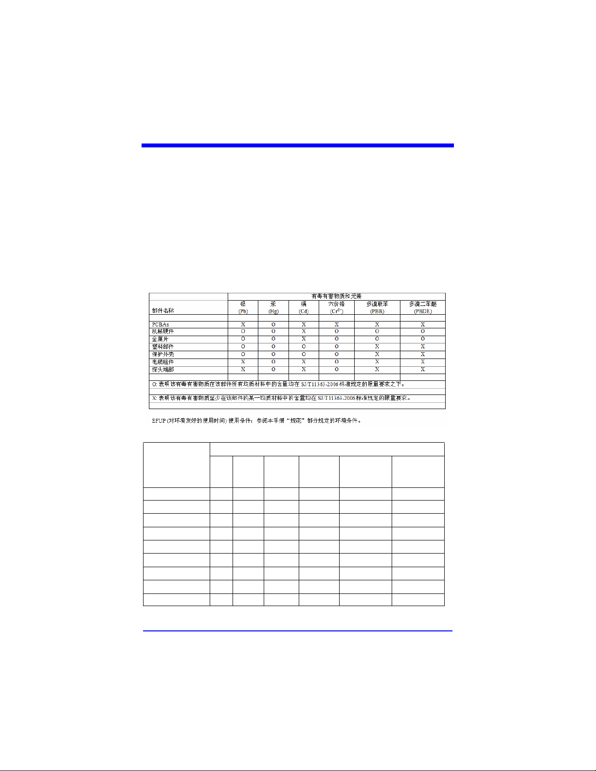
Toxic or Hazardous Substances and Elements
6+
)
Polybrominated
Biphenyls
(PBB)
Part Name Lead
PCBAs X O X X X X
Mechanical Hardware O O X O O O
Sheet Metal O O X O O O
Plastic Parts O O O O X X
Protective Case O O O O X X
Cable Assemblies X O X O X X
Probe Tips X O X O X X
(Pb)
Mercury
(Hg)
Cadmium
(Cd)
Hexavalent
Chromium
(Cr
Polybrominated
Diphenyl Ethers
(PBDE)
9–4 ZS1500-OM-E Rev C
Page 47

Specifications
O: Indicates that this toxic or hazardous substance contained in all of the homogeneous materials for this part is
below the limit requirement specified in SJ/T11363-2006.
X: Indicates that this toxic or hazardous substance contained in at least one of the homogenous materials used for
this part is above the limit requirement specified in SJ/T11363-2006.
EFUP (Environmental Friendly Use Period) Use Conditions: refer to the environmental
conditions stated in the specifications section of this Manual.
###
ZS1500-OM-E Rev C 9–5
Page 48

ZS1500 High Impedance Active Probe
BLANK PAGE
9–6 ZS1500-OM-E Rev C
Page 49

Appendix A
Appendix A
PERFORMANCE VERIFICATION TEST RECORD
This record can be used to record the results of measurements made
during the performance verification of the ZS1500 High Impedance
Active Probe.
Photocopy this page and record the results on the copy. File the completed record as required by applicable internal quality procedures.
The section in the test record corresponds to the parameters tested in
the performance verification procedure. The numbers preceding the
individual data records correspond to the steps in the procedure that
require the recording of data. Results to be recorded in the column
labeled “Test Result” are the actual specification limit check. The test
limits are included in all of these steps. Other measurements and the
results of intermediate calculations that support the limit check are to be
recorded in the column labeled “Intermediate Results”.
Permission is granted to reproduce these pages for the purpose of
recording test results.
Probe Model: ZS1500___________________
Serial Number: _________________________
Asset or Tracking Number: _________________________
Date: _________________________
Technician: _________________________
ZS1500-OM-E Rev C A–1
Page 50

ZS1500 High Impedance Active Probe
EQUIPMENT USED:
MODEL SERIAL
OSCILLOSCOPE
DIGITAL MULTIMETER
FUNCTION
GENERATOR
1
The function generator used in this Performance Verification Procedure is used for making relative measurements. The output of the generator is measured with a DMM or
oscilloscope in this procedure. Thus, the generator is not required to be calibrated.
1
NUMBER
CALIBRATION
DUE DATE
N/A
ZS1500 TEST RECORD
Step Description Intermediate data
Test Result
Output Zero Voltage
A-5 Output Zero Voltage (Test limit ≤ ±800 µV)_____________ V
LF Attenuation Accuracy
B-7 Generator Output Voltage ______________ V
B-8 Expected Output Voltage, top range ______________ V
B-10 Measured Output Voltage, top range ______________ V
B-12 Gain Error, top range (Test limit ≤ ±1.0%) ______________%
B-17 Generator Output Voltage ______________ V
B-19 Expected Output Voltage, mid range ______________ V
B-21 Measured Output Voltage, mid range ______________ V
B-23 Gain Error, mid range (Test limit ≤ ±1.0%) ______________%
###
A–2 ZS1500-OM-E Rev C
Page 51

Appendix A
Notes
_______________________________________________________
_______________________________________________________
_______________________________________________________
_______________________________________________________
_______________________________________________________
_______________________________________________________
_______________________________________________________
_______________________________________________________
_______________________________________________________
_______________________________________________________
_______________________________________________________
_______________________________________________________
_______________________________________________________
_______________________________________________________
_______________________________________________________
_______________________________________________________
_______________________________________________________
_______________________________________________________
_______________________________________________________
_______________________________________________________
_______________________________________________________
_______________________________________________________
_______________________________________________________
_______________________________________________________
_______________________________________________________
_______________________________________________________
ZS1500-OM-E Rev C A–3
Page 52

ZS1500 High Impedance Active Probe
Notes
_______________________________________________________
_______________________________________________________
_______________________________________________________
_______________________________________________________
_______________________________________________________
_______________________________________________________
_______________________________________________________
_______________________________________________________
_______________________________________________________
_______________________________________________________
_______________________________________________________
_______________________________________________________
_______________________________________________________
_______________________________________________________
_______________________________________________________
_______________________________________________________
_______________________________________________________
_______________________________________________________
_______________________________________________________
_______________________________________________________
_______________________________________________________
_______________________________________________________
_______________________________________________________
_______________________________________________________
_______________________________________________________
_______________________________________________________
A–4 ZS1500-OM-E Rev C
 Loading...