

Page 1

2SHUDWLRQ
The input circuits in the AP034 Activ e Differ ential
Probe incorporate components that protect the
probe from damage resulting from electrostatic
discharge (ESD). Keep in mind that this is an
active probe, and it should be handled carefully
to avoid damage. When using the AP034 Active
Differential Probe, you are advised to take
precautions against potential instrument damage
due to ESD.
CONNECTING THE PROBE TO THE TEST INSTRUMENT
When you are using the AP034 Active Dif ferential Probe with a
LeCroy Oscilloscope equipped with ProBus, attach the probe
output connector to the oscilloscope input connector. The
oscilloscope will recognize the probe, set the oscilloscope input
termination to 50 DQG DFWLYDWH WKH SUREH FRQWURO IXQFWLRQV LQ
the user interface.
2SHUDWLRQ
Caution
To use the AP034 Active Differ ential Probe with instrumentation
not equipped with a ProBus interface, it is necessar y to use the
ADPPS Power Supply. Attach the ADPPS connector to the probe
output connector. The output connector of the ADPPS is a
standard male BNC that can be directly connected to another
instrument. If necessary, the output of the ADPPS can be
interconnected with a 50 FRD[LDOFDEOH7RPLQLPL]HWKHHIIHFWV
of skin loss, this cable should be 1 m or less in length. The
AP034 Active Differential Probe is des igned to drive a 50 ORDG
The gain will be uncalibrated if the output is not correctly
terminated. If you are using the probe with an instrument with a
high input impedance, place a 50 %1&LQOLQHWHUPLQDWRURQWKH
instrument input before attaching the ADPPS.
CONNECTING THE PROBE TO THE TEST CIRCUIT
At the probe tip, two inputs and a ground connection are
available for connecting the probe to a circuit under test. For
accurate measurem ents, both the + and – inputs m ust always be
AP034-OM-E Rev D ISSUED: January 2000 ²
Page 2

$3$FWLYH3UREH
connected to the test circuit. The ground connection is optional.
Positive voltages applied to the + input relative to the – input will
deflect the oscilloscope trace toward the top of the screen.
To maintain the high performance capability of the probe in
measurement applic ations, user care in connecting the probe to
the test circuit. Increasing the parasitic capacitance or inductance
in the input paths may introduce a “ring,” or slow the rise time of
fast signals. To m inimize these effects, use the shortest length
possible when connecting the probe to the circuit under test.
Input leads that form a large loop area (even shielded coaxial
cables) will pick up any radiated magnetic field that passes
through the loop, and may induce noise in the probe inputs.
Because this signal will appear as a diffe rential mode signal, the
probe’s common mode rejection will not remove it. You can
greatly reduce this effect by using short interconnection leads,
and twisting them together to minimize the loop area.
High common mode rejection requires precise matching of the
relative gain or attenuation in the + and – input signal paths.
Mismatches in additional parasitic capacitance, inductance,
delay, and a source impedance differ ence between the + and –
signal paths will lower the common mode rejection ratio.
Therefore, it is desirable to us e the sam e length and type of wire
and connectors for both input connections . W hen possible, try to
connect the inputs to points in the circuit with approxim ately the
same source impedance.
If AC coupling is desired, install the AC coupling accessory on
the probe tip before connecting it to the test circuit. The low-
frequency cutoff (–3 dB point) of the AC coupler is approxim ately
16 Hz.
If the voltage in the test circuit exceeds the probe’s capability,
add the external ÷10 or ÷20 attenuator* to the probe tip. If both
the external attenuator and AC coupler are used, install the
attenuator on the probe tip first, then install the AC coupler on the
attenuator input.
* Note
The external attenuators are precisely adjusted
during manufacturing to match the
² ISSUED: January 2000 AP034-OM-E Rev D
Page 3

2SHUDWLRQ
characteristics of the input of the probe with
which they were shipped. The input
characteristics of the external attenuator itself do
not exactly match those of the probe. Therefore,
using the ÷10 and ÷20 attenuators at the same
time is not recommended. The scale factor
encoding system will not operate correctly with
both attenuators installed simultaneously.
The input characteristics of the AP034 1 GHz
Active Differential Probe are significantly
different than those of the AP033 500 MHz
Active Differential Probe. The external
attenuators are not interchangeable. The
external attenuators currently supplied with the
probes are labeled with the appropriate model
number. The attenuators supplied with model
AP033 probes prior to the introduction of the
AP034 did not include the model number on the
label. When using an external attenuator with the
AP034 Active Differential Probe, make sure it is
labeled “AP034.”
Interchanging non-compatible attenuators will
not damage the probes; however, the transient
response of the measured signals will be
significantly in error.
In addition to being compatible with the included lead set, the
probe input connectors will mate with standard 0.025 in.
(0.635 mm) square pins in any rotational orientation. To avoid
damaging the input connectors, do not attempt to insert
connectors or wire larger than 0.036 in. (0.91 m m) in diameter.
Avoid rotating square pins after they are inserted into the input
connectors.
The included accessories simplify the task of connecting the
probe to the test circuit:
• Use the small (0.5 mm) mini clips with the flexible
lead set when connecting to fine-pitch surface mount
IC leads.
AP034-OM-E Rev D ISSUED: January 2000 ²
Page 4
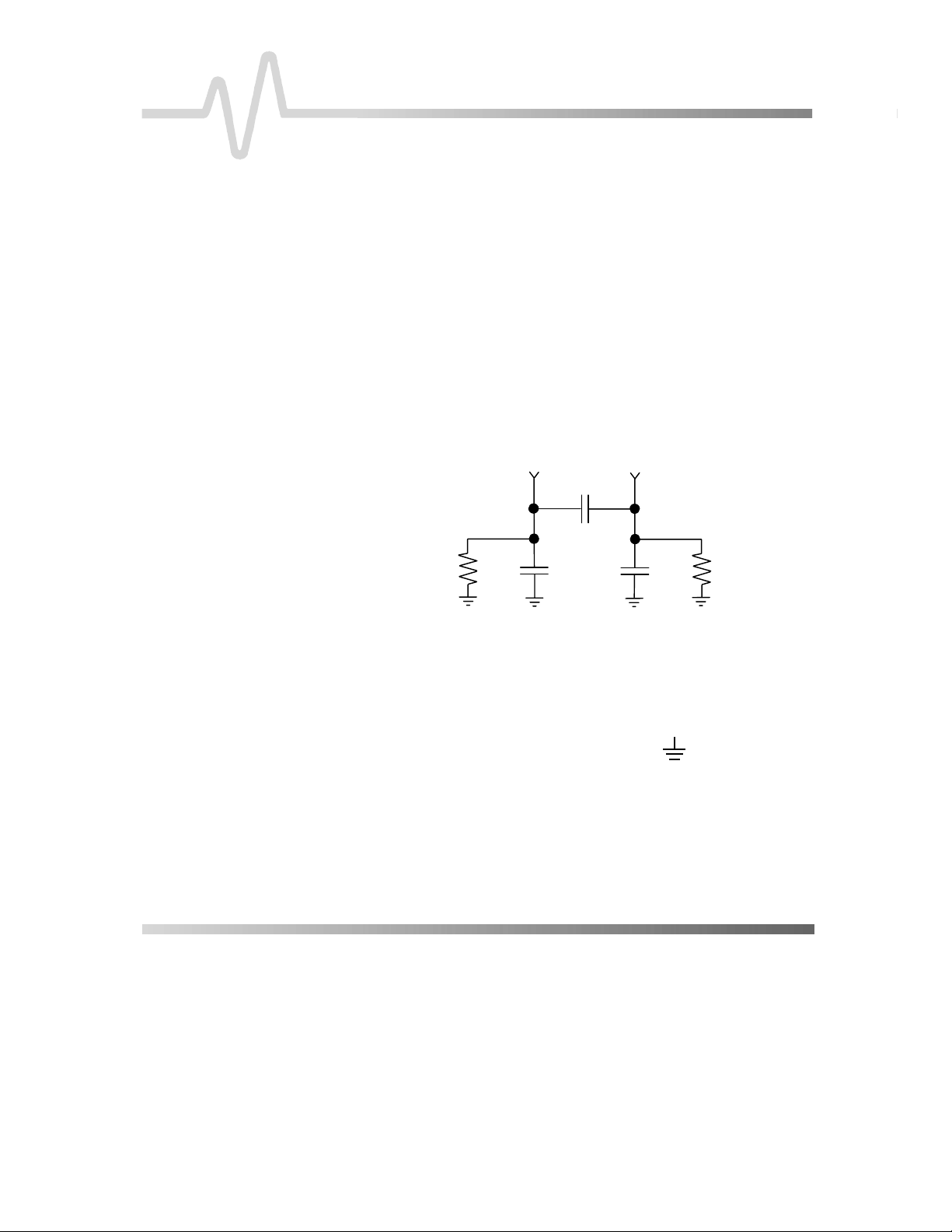
PROBE INPUT LOADING
$3$FWLYH3UREH
• The larger (0.8 mm) mini clips can be used to
connect to through-hole leaded components.
• The offset round pins can be used for hand-held
probing applications. Reposition the pins by rotating
them to obtain the required spacing.
Attaching any probe to a test circuit will add some loading. In
most applications, the high impedance of the AP034 Active
Differential Probe inputs im parts an insignificant load to the test
circuit. However at very high frequencies, the capacitive
reactance of the probe’s input capacitance may load the circuit
enough to affect meas urement accuracy. The equivalent model
of the probe input circuits is shown below:
GROUNDING THE PROBE
+
≈ 0.1 pF
1.5 pF
1 MΩ
Figure 1. AP034 Equivalent Input Model
The single lead along with one of the larger (0.8 mm) m ini clips
can be used to ground the probe to the test circuit. Insert the pin
end of the lead into the receptacle marked:
Note
Do not use the attenuator encoding receptacle
(unmarked socket near the – input) to ground the
probe. Connecting to the encoding receptacle
will not provide adequate grounding, and may
result in in correct scale factor indication.
-
1.5 pF
1 MΩ
² ISSUED: January 2000 AP034-OM-E Rev D
Page 5

2SHUDWLRQ
In most cases it is not necessary to ground the probe to the
circuit under test. However, if the test circuit is isolated from earth
ground, it is usually necessary to connect the probe ground to a
point in the circuit. Grounding test circuits that are referenc ed to
earth ground may improve the fidelity of high-frequency
components in the waveforms. The potential for improvement
with grounding will vary depending on the common mode source
impedance. However, connecting the probe ground to a circuit
that is referenced to earth ground c an create a ground loop that
may add noise to low-amplitude signals*. Rejection of highfrequency common mode signals is improved when the probe
head is ungrounded.
The best recomm endation for connecting or not connecting the
probe ground is to try both configurations and select the one that
performs the best.
Note
The AP034 Active Differential Probe transmits
the measured signal differentially through the
probe cable. This essentially eliminates signal
degradation from ground loop effects within the
probe. However, creating a ground loop may
introduce signal distortions in the test circuit
itself, or in any coaxial cable between the
ADPPS power supply and the test instrument.
AP034-OM-E Rev D ISSUED: January 2000 ²
Page 6

SELECTING THE PROPER RANGE
The AP034 Active Differential Probe has a fixed gain of X1
(unity). Use of the ÷10 or ÷20 external attenuators reduces the
amplitude of the input signal when it is necess ary to extend the
dynamic operating range of the probe. Attenuating the input
signal increases both the differential mode range and common
mode range of the probe.
Refer to the block diagram below.
$3$FWLYH3UREH
ControlProbe
+
1
-
1
By using the plug-on attenuator, you can extend the attenuation
range to ÷20. Do not use the ÷10 and ÷20 plug-on attenuators
simultaneously. The maxim um ranges are given in the f ollowing
table:
Table 1. AP034 Dynamic ranges and i nput capacitance at different attenuator
Common Mode Range
Differential Mode Range *
X1
Σ
+
V
Offs
Σ
X1
Figure 2. AP034 Block Diagram
settings
÷1
Attenuation
(Probe Only)
±16 V ±42 V ±42 V
±400 mV ±4 V ±8 V
*Offset moves the center point of this range.
Attenuation
+
-
÷10
X1
50
÷20
Attenuation
² ISSUED: January 2000 AP034-OM-E Rev D
Page 7

When us ing a differential probe or amplifier, be ca reful to avoid
exceeding the common mode range. Because the common
mode signal is rejected by the differential probe, and is not
displayed, changes in the amplitude of the common mode
component are not apparent to the user. Exceeding the c omm on
mode range may introduce distortion into the AP034 output.
Circuitry in the probe detects the presence of either attenuator,
and displays the effective gain of the probe on the probe front
panel.
OPERATION WITH LECROY OSCILLOSCOPES
When the AP034 probe is connected to a LeCroy oscilloscope
equipped with ProBus interface, the displayed scale fac tor will be
adjusted to account for the effective gain of the probe. The
channel O
FFSET knob will control the probe offset, rather than the
offset at the oscilloscope input. The probe contr ol menu can be
activated by pressing the COUPLING button while the channel to
which the probe is attached is selected.
2SHUDWLRQ
Figure 3. AP034 Probe Control Menu
AP034-OM-E Rev D ISSUED: January 2000 ²
Page 8

When the AP034 Active Differential Probe is first connected to
the oscilloscope, the following message will appear:
“WARNING: Probe offset buttons are locked.” This alerts you
that offset control m ust be m ade through the os cilloscope, rather
than through the buttons located on the probe. It does not
indicate a failure in the probe or oscilloscope.
Correct display of scale factor with the ÷20
attenuator installed and correct operation of
probe offset require that software version 8.1 or
higher be loaded. Refer to the manual section
“Oscilloscope Software Compatibility” for
additional information.
AP034 USE WITH THE ADPPS POWER SUPPLY
The optional ADPPS Power Supply allows the AP034 Active
Differential Probe to be used with instruments that are not
equipped with the ProBus interface. When used with the ADPPS,
the AP034 must be terminated into 50 ,I WKH WHVW LQVWUXPHQW
input impedance is not 50 LQVHUW D LQOLQH WHUPLQDWRU
between the ADPPS and the instrument input. If a coaxial
extension cable is used, the terminator should be located at the
instrument end of the cable. Note that the additional parasitic
losses of extension cables may reduce the usable bandwidth of
the system below the AP034 specification.
$3$FWLYH3UREH
Note:
To prevent signal distortion, it is necessary to keep the AP034
output less than 400 mV at all times.
With the ProBus interface (see note on following page), the
oscilloscope O
Without the ProBus, it is acceptable to use the oscilloscope to
position the waveform at high sensitivities , but it is a practic e that
can lead to erroneous measurements when the probe output
exceeds ±400 mV. Therefore, when the ADPPS is used, it is
preferable to use the AP034 offset function to perform all
waveform positioning.
The AP034 offset allows you to measure signals up to 2.0 V
(1.6 V of offset plus 400 mV of output signal). With accessory
plug-on attenuators, the effective offset is increased, and input
signals of 20 V (÷10) or 40 V (÷20) may be viewed. The peak
² ISSUED: January 2000 AP034-OM-E Rev D
FFSET control actually controls the AP034 offset.
Page 9

2SHUDWLRQ
signal that can be viewed at any equivalent scale factor is the
Input Differential Mode Range plus the off set used. See Adding
Offset on the following page.
When using the AP034 with the ADPPS power supply on
oscilloscopes without ProBus interface, use the following table to
select the desired effec tive volts per division and determine the
offset available.
Equivalent
Scale
Oscilloscope
Scale Factor
Factor
2 mV/Div 2 mV/Div
5 mV/Div 5 mV/Div
10 mV/Div 10 mV/Div
20 mV/Div 20 mV/Div
50 mV/Div 50 mV/Div
100 mV/Div 100 mV/Div
200 mV/Div 20 mV/Div
500 mV/Div 50 mV/Div
1 V/Div 100 mV/Div
2 V/Div 100 mV/Div
Table 2. Recommended AP034 and Os cilloscope settings to obt ain desired
AP034
Attenuation
Common
Mode Range
÷1 ±16V ±8 mV
÷1 ±16 V ±20 mV
÷1 ±16 V ±40 mV
÷1 ±16 V ±80 mV
÷1 ±16 V ±200 mV
÷1 ±16 V ±400 mV
1
÷10
÷10
÷10
÷20
1
1
1
1
2
3
±42 V ±800 mV
±42 V ±2 V
±42 V ±4 V
±42 V ±8 V
Attenuation obtained using t he external ÷10 or ÷20 attenuator.
Input differential mode range displayed is limi ted by ±4 divisions of vertical
scale on oscilloscope.
Limited by probe output and ±4 divisions of vertical scale on oscilloscope.
Oscilloscope OFFSET and POSITI ON must be set to zero.
equivalent Volts/Divi sion
Input
Differential
Mode Range
2
2
2
2
2
3
2
2
3
3
Maximum
Offset
Maximum
Observable
Signal with
Offset
±1.6 V ±1.608 V
±1.6 V ±1.620 V
±1.6 V ±1.640 V
±1.6 V ±1.680 V
±1.6 V ±1.800 V
±1.6 V ±2.0 V
±16 V ±16.8 V
±16 V ±18 V
±16 V ±20 V
±32 V ±40 V
Input Noise
(nV/√Hz),
Typical
35
35
35
35
35
35
350
350
350
700
AP034-OM-E Rev D ISSUED: January 2000 ²
Page 10

ADDING OFFSET
$3$FWLYH3UREH
The AP034 Active Differential Probe has true differential offset
capability. This allows you to remove a DC bias voltage from the
differential input signal while maintaining DC coupling. By using
probe offset rather than the P
the full dynamic range of the probe remains centered around the
offset level.
OSITION control on the oscilloscope,
+700 mV
+500 mV
+300 mV
0 mV
Input Differential
Waveform
+700 mV
+500 mV
+400 mV
+300 mV
0 mV
-400 mV
Waveform “clipped”
+700 mV
±400 mV window
re-centered around
the probe offset.
with no offset
+500 mV
+300 mV
±400 mV
centered
at 0 V
Figure 4. Effect of Dif f erential Offset
0 mV
Offset used to re-center
the differential dynami c
range around +500 mV
When the AP034 Active Differential Probe is used with a LeCroy
oscilloscope equipped with ProBus interface, the probe offset
can be controlled with the channel O
FFSET knob.* The buttons on
the probe housing will be disabled.
When used with the ADPPS Power Supply on instruments that
lack ProBus support, of fset can be c ontrolled with the buttons on
the probe’s front panel. The offset can be returned to zero at any
time by briefly pressing both the Î and Ï O
same time. Pres sing both the Î and Ï O
FFSET buttons at the
FFSET buttons for more
than 2 seconds will initiate an Autobalance cycle.
*Note
Probe offset is controlled with the channel
O
FFSET knob in oscilloscope software versions
8.1.0 or higher. The current offset value is
² ISSUED: January 2000 AP034-OM-E Rev D
Page 11

AUTOBALANCE
2SHUDWLRQ
displayed above the graticule for a few seconds
after a change is made by turning the knob (refer
to Figure 3). In prior software versions, the
channel O
oscilloscope input rather than the probe offset.
When the AP034 Active Differential Probe is
used with LeCroy oscilloscopes with older
software versions, it is important that the channel
offset (controlled by the channel O
remain set to 0.0000 V. Moving the displayed
waveform with the channel offset rather than
probe offset will not re-center the dynamic
operating range of the probe. Offsetting the trace
with the oscilloscope channel offset introduces
the possibility of erroneous waveforms that result
from overloading the probe.
The AP034 Active Differential Probe incorporates an
Autobalance function to remove the DC offset from the output.
Autobalance must be invoked by you. When power is first
applied, the probe will return to the internal values resulting from
the last Autobalance cycle. For Autobalance to function properly,
all signals must be removed from the input.
FFSET knob adjusted the offset of the
FFSET knob)
After several minutes of warmup, or when the probe is exposed
to a large shift in ambient tem perature, s ome DC off set dr ift m ay
occur from thermal ef fects in the am plifier cir cuitry. To initiate an
Autobalance cycle, remove the probe from the test circuit and
select the AUTOBALANCE menu selection in the oscilloscope
“COUPLING” menu for the channel the probe is c onnected to. If
the probe is being used with the ADPPS power supply, remove
the input signal, then push and hold both O
FFSET buttons for two
seconds. The AP034 must be terminated into 50 IRUVXFFHVVIXO
Autobalance.
Upon successful completion of the Autobalanc e c ycle, all three of
the EFFECTIVE GAIN indicators will be briefly illuminated. If an
input signal is present during auto balance and the routine fails ,
the EFFECTIVE GAIN indicators will not illuminate. The probe
will then revert to the offset values resulting from the last
AP034-OM-E Rev D ISSUED: January 2000 ²
Page 12

successful completion of the Autobalance cycle. In many
situations, this will be adequate to make routine measurements.
DESIGNING TEST FIXTURES FOR THE AP034 PROBE
Often it is desirable to connect the probe directly to userfabricated test fixtures, such as those used for semiconductor
characterization. To facilitate use with custom test fixtures, the
input receptacles used in the AP034 probe are compatible with
commercially available 0.025 in. (0.635 mm) square pins. The
receptacles do not require a specif ic rotational orientation for the
square pin. The dimensions listed below can be used as a layout
guide for a test fixture circuit board. T he recomm ended insertion
depth of the pins is 0.100 in. (2.5 mm) to 0.200 in. (5.0 mm).
Top View
Looking toward circuit board
$3$FWLYH3UREH
Side View
0.100”-
0.200”
0.110”
0.105”
0.170”
0.100”
Figure 5. Layout dimensions f or test fixtures
0.025” REF.
# # #
² ISSUED: January 2000 AP034-OM-E Rev D
 Loading...