

Page 1

I OPERAToR’s MANUAL I
,|, ......................
i i i in it
- i li I I I II I
~ "- i~_.
MODEL 9100 SERIES
April 1993
Page 2
[ TABLE OF CONTENTS
1 General Information
Purpose
Unpacking and Inspection
Warranty
Product Asskmnce
Maintenance Agreements
Documentation Discrepancies
Software Licensing Agreement
Service Procedure
2 Product Description
9100 System Description 2-1
9100 Waveform Generation Concept
91 O0 Architecture 2-3
Front Panel Controls, Connections and Indicators 2-11
Rear Panel Controls, and Connections 2-13
Specifications 2-15
$ Operations
Preparation For Use 3-1
Standard Functions 3-3
Arbitrary Waveforms and File Conventions
Defining An Arbitrary Waveform In Terms
OfA Waveform File
Transferring Waveform Data Files Into the
AFG RAM Disk Via GPIB 3--6
Loading the Waveform Files From RAM Disk
Into the Waveform Generator Circuit 3-9
Control Settings Summnry-(amplitude, dock, ...) 3-12
Specifying How the Data Values Are
Convened to Voltage Levels 3-13
Spedfying the Time Per Point 3-14
Specifying The Trigger Mode 3-14
Specifying the Trigger Delay 3-27
Specifying External Triggering 3-27
Using the Filters to Smooth the Waveform 3-27
Disconnecting the Output While the Generator
is Running 3-28
Inverting Channel 1 or 2
Summing Channel 1 and Channel 2 Signals
Using the External Sum Input
Using an External Clock Reference 3-29
Using an External Clock Source 3-29
Synchronizing with Another 9100 Series AFG 3-29
Starting and Stopping the Waveform
1-1
1-I
1-1
1-2
1-9
1-2
1-2
1-3
2-2
3--4
3-5
3-28
3-28
3-28
3-30
Page 3
I TABLE OF CONTENTS I
Automating the Setup and Loading of Waveforms 3-30
4 Operating Instructions
Control Panel Operation 4-1
Basic Description 4-1
Main Menu Keys
Understanding the 9100/CP Menus 4-11
Entry Changes 4-19
Controlling the Arbitrary Function Generator
with the 9100/CP
Selecting an Arbitrary Waveform 4-23
Selecting a Standard Waveform
Selecting Attributes of Standard Sine 4-26
Selecting Attributes of Standard Square 4--27
Selecting Attributes of Standard Triangle 4-28
Selecting Attributes of Standard Ramp 4-28
Selecting Attributes of Standard Pulse 4-29
Selecting Attributes of Standard DC
Channel 1 Waveform Attributes 4-30
Channel 2 Waveform Attributes 4-33
Controlling the Tunebase 4--33
Trigger Control
Arming and Firing Trigger
Working with Setup Files
Working with Sequence Files
Loading and Linking Waveforms ~ ~3
Executing Waveforms
Aborting Waveforms
Accessing the State of the AFG
4-5
’ 4-22
4-25
4-30
4--37
~ ~0
~ ".0
~ ~2
~ ~5
~ ~5
~ ~5
5 Operating over the GPIB
Genera]
Introduction
Remote Mode
Local Mode
Addressing
Messages
Device Dependent Messages
Message Input Format
Command Format
Command Parameters
General Rules for Commands
IEEE-488 Standard Messages
Receiving the Device Clear Message
Receiving the Trigger Message
5-1
5-1
5-1
5-1
5-2
5-2
5-2
5-3
5-3
5--4
5-5
5-5
5-5
Page 4
l TABLE OF CONTENTS
Receiving the Remote Message
Receiving the Local Message
Receiving the Local Lockout Messages
Sending Messages
Sending the Require Service Message (SRQ)
Sending the Serial Poll Status Byte
Sending the Secondary Status Bytes
Operation of the Status Bytes
Acronym Guidelines
Programming Command Reference Section
Command Summary
File Handling Commands
File Structures
Setup and Sequence Files
Setup Files
Executing Setup Files
Sequence Files
Executing Sequence Files
Single Waveform Files
Dual Waveform Files
Executing Waveform Files
File Handling Commands
DELETE
END
LEARN_SETUP
LINK
LOAD
RECAIJ~
SEQUENCE
SETUP
STORE
Action Commands
ABORT
ARBITRARY
ARM
CALIBRATE
CI.FAR
GO
NEXT
SELFTEST
STOP
TRIGGER
Channel Parameter Commands
CH 1 AMPLITUDE (CH2_AMPLITUDE)
CH I"FILTER (CH2_FILTER)
5-5
5-5
5-5
5-6
5-6
5-6
5-7
5-7
5-14
5-15
5-18
5-18
5-19
5-19
5-20
5-20
5-21
5-22
5-22
5-23
5-24
5-25
5-26
5-27
5-29
5-30
5-31
5-32
5-33
5-34
5-35
5-36
5-37
5-38
5-39
5-40
5-41
5-42
5-43
5-44
5-45
Page 5

TABLE OF CONTENTS
CH l_I NVERT (CH2_I NVERT)
CHI OFFSET (CH2_OFFSET)
CHI__.OLrI~UT (CH2_OUTPUT)
CH I_ZERO_REF (CH I_ZERO_REF)
EXTERNAL SUM
SUM_MODI~
Timebase Commands
CLOCK_SOURCE
CLOCK_LEVEL
CLOCK_MODE
CLOCX_RA~
CLOCK_SLOPE
CLOCKPERIOD
CLOCKREFERENCE
Trigger Commands
DELAY MODE
MARKI~R DELAY
TRIGGEI~ ARM SOURCE
TRIGGER_-DELAY
TRIGGER_LEVEL
TRIGGER_MODE
TRIGGER_SLOPE
TRIGGER_SOURCE
Standard Function Commands
STANDARD
SINE
SINE_MODE
SINE_FREQUENCY
SINE CHI PHASE
SINE_-CH2-_PHASE
SQUARE
SQUARE_MODE
SQUARE_FREQUENCY
SQUARE_PHASE
SQUARE_P.ELATIVE_PHASE
TRIANGLE
TRLkNGLE_MODE
TR/ANGLE FREQUENCY
TRIANGLE_PHASE
TRIANGLE_RELATIVE_PHASE
RAMP
RAMP_MODE
RAMP_PERIOD
RAMP_PHASE
5--46
5-47
5-48
5-49
5-50
5-51
5-52
5-53
5-54
5-55
5-56
5-57
5-58
5-59
5-60
5-61
5-62
5--63
5--64
5-65
5--66
5-68
5-69
5-70
5-71
5-72
5-73
5-74
5-75
5-76
5-77
5-78
5-79
5-80
5-81
5-82
5-83
5-84
5-85
5-86
5-87
Page 6
TABLE OF CONTENTS I
RAMP_RELATIVE_PHASE
PULSE
PULSE_WIDTH
PULSE_PERIOD
PULSE DELAY
PULSE-OPTIMIZE
DC
DC_MODE
Query Type Commands
ACTIVE FILES
FUNCTION
EXIST
DIRECTORY
IDENTIFY
MEMORY
VIEW
Communication Commands
COMM_FORMAT
COMM_HEADER
MASK
STB
TSTB
COMMAND SUMMARY
Figure 5.1 - Heirarchical Structure Of The 9100
Status Bytes
Table 5.1 -Status Byte Bit Assignments
Table 5.2 - Error Codes
Table 5.3 - 9100 GPIB Acronyms
5--88
5-89
5-90
5-91
5-92
5-93
5-94
5-95
5-96
5-97
5--98
5-99
5-101
5-102
5-103
5-105
5-106
5-107
5-108
5-109
5-110
5-9
5-10
5-11
5-14
6 RS--232-Interface
Selecting the RS-232C Interface
Configuring the RS--232C Interface
Using RS-232
Typical RS-232C Dialog
RS-232 Commands
COMM_RS_CONF
COMM_PROMPT
COMM_RS_SRQ
6-1
6-1
6-2
6-3
6--4
6--6
6-7
Page 7
]TABLE OF CONTENTS I
7 Model 9109
General Description
High Speed Memory
Digital Output Specifications
Reconfiguring the Digital Output
Interconnection Information
Application InformatiOn
9109 Front Panel Diagram
7-1
7-1
7-1
7-4
7-6
7-10
7-12
8 Model 9101
Introduction
Differences Between 9101 and 9100
9101 Front Panel Diagram
9 9100/MM, /MM1,/MM2
Description
U.ing The Memory Expamion Option
Using The Control Memory Image Functions
Learning A CMI File
Deleting A CMI File
Reviewing The Contents ofA CMI File
10 9100/RT
Introduction
Verifying Installation
Functional Description
9100/RT LOAD and LINK Comands
FIFO Memory Commands
External FIFO Loading
FIFO Reading
F..yamples of Operation
External Real-Time Port
Using the 9100/RT Option
Using the External Real-Time Port
Waveform Selection Using BASICA
Specifications
8-1
8-1
8-4
9..-1
9--2
9--3
9-3
9--5
9-6
10-I
10-1
10-2
10-4
1 0-5
10--6
10--8
10-9
10-10
10-11
10-15
10-17
10-19
Appendix I
Index
Page 8
1
GENERAl, INFORMATION
"
PURPOSE
UNPACKING AND
INSPECTION
WARRANTY LeCroy warrants its instrument products to operate within speci-
This manual is intended to provide instruction regarding the
setup and operation of the covered instruments. In addition, it
describes the theory of operation and presents other information
regarding its functioning and application.
The Service Documentation, packaged separately, should be
consulted for the schematics, parts lists and other materials that
apply to the specific version of the instrument as identified by
its ECO number.
LeCroy recommends that the shipment be thoroughly inspected
immediately upon delivery. All material in the container(s)
should be checked against the enclosed Packing List and shortages reported to the carrier promptIy. If the shipment is damaged in any way, please notify the carrier. If the damage is due
to mishandling during shipment, you must file a damage claim
with the carrier. The LeCroy field service office can help with
this. LeCroy tests all products before shipping and packages all
products in containers designed to protect against reasonable
shock and vibration.
fications under normal use and service for a period of one year
from the date of shipment. Component products, replacement
parts, and repairs are warranted for 90 days. This warranty ex-
tends only to the original purchaser. Software is thoroughly
tested, but is supplied "as is" with no warranty of any kind cov-
ering detailed performance. Accessory products not manufac-
tured by LeCroy are covered by the original equipment manu-
facturers warranty only.
In exercising this warranty, LeCroy will repair or, at its option,
replace any product returned to the Customer Service Depart-
ment or an authorized service facility within the warranty pe-
riod, provided that the warrantor’s examination discloses that
the product is defective due to workmanship or materials and
has not been caused by misuse, neglect, accident or abnormal
conditions or operations.
The purchaser is responsible for the transportation and insur-
ance charges arising from the return of products to the servicing
facility. LeCroy will return all in-warranty products with trans-
portation prepaid.
This warranty is in lieu of all other warranties, express or im-
plied, including but not limited to any implied warranty of mer-
1-1
Page 9
General Information
chantability, fitness, or adequacy for any particular purpose or
use. LeCroy shall not be liable for any special, incidental, or
consequential damages, whether in contract, or otherwise.
PRODUCT ASSISTANCE
MAINTENANCE
AGREEMENTS
DOCUMENTATION
DISCREPANCIES
SOFTWARE LICENSING
AGREEMENT
Answers to questions concerning installation, calibration, and
use of LeCroy equipment are available from the SSD Customer
Services Department, 700 Chestnut Ridge Road, Chestnut
Ridge, New York 10977-6499, (914) 578-6020, or your local
field service office.
LeCroy offers a selection of customer support services. For example, Maintenance agreements provide extended warranty that
allows the customer to budget maintenance costs after the initial
warranty has expired. Other services such as installation, training, on-site repair, and addition of engineering improvements
are available through specific Supplemental Support Agreements.
Please contact the Customer Service Department or the local
field service office for details.
LeCroy is committed to providing state-of-the-art instrumenta-
tion and is continually refining and improving the performance
of its products. While physical modifications can be imple-
mented quite rapidly, the corrected documentation frequently
requires more time to produce. Consequently, this manual may
not agree in every detail with the accompanying product and the
schematics in the Service Documentation. There may be small
discrepancies in the values of components for the purposes of
pulse shape, timing, offset, etc., and, occasionally, minor logic
changes. Where any such inconsistencies exist, please be assured that the unit is correct and incorporates the most up-todate circuitry.
Software products are licensed for a single machine. Under this
license you may:
1-2
¯ Copy the software for backup or modification purposes in sup-
port of your use of the software on a single machine.
¯ Modify the software and/or merge it into another program for
your use on a single machine.
¯ Transfer the software and the license to another party if the
other party accepts the terms of this agreement and you relin-
Page 10
General Information 1
quish all copies, whether in printed or machine readable form,
including all modified or merged versions.
SERVICE PROCEDURE Products requiring maintenance should be returned to an
authorized service facility. If under warranty, LeCroy will repair
or replace the product at no charge. The purchaser is only responsible for the transportation charges arising from return of
the goods to the service facility.
For all LeCroy products in need of repair after the warranty
period, the customer must provide a Purchase Order Number
before any inoperative equipment can be repaired or replaced.
The customer will be billed for the parts and labor for the repair as well as for shipping.
All products returned for repair should be identified by the
model and serial numbers and include a description of the defect or failure; name and phone number of the user. In the
case of products returned, a Return Authorization Number is
required and may be obtained by contacting the Customer gerv-
ice Department in your area.
New York Corporate Headquarters
East Coast Regional Service
New Hampshire
Virginia
New Mexico
California
(914)
(914)
(603)
(703) 368-1033
(505)
(415) 463-2600
425-2000 or
578-6059
627-6303
293-8100
1-3
Page 11
2
9100 SYSTEM
DESCRIPTION
9100, 9101, 9109
9100R
9100/CP
9100/SW
9100GPIB2
PRODUCT DESCRIPTION
The LeCroy 9100 Series Arbitrary Function Generators (AFG)
are high performance ATE or benchtop instruments which can
generate either standard or user-defined, complex waveforms
with unparalleled point-to-point resolution. They are fully programmable via either GPIB or RS-232. Wavef6rm creation and
editing software is offered for PC-DOS compatible computers.
The products in the 9100 Series are:
9100 high speed dual channel Arbitrary Function Generator
9101 high speed single channel Aribitrary Function Generator
9109 high speed dual channel Arbitrary Function Generator
with digital outputs.The common elements of the 9100 Series
are described in the early chapters of this manual. Product spe-
cific information for the 9109 and 9101 is located in Chapter 7
and 8 respectively.
The 9100 Series instruments are part of a complete custom
waveform generation system. The main products which support
this system are listed below.
ARBITRARY FUNCTION GENERATOR MAINFRAME. This
is the basic mainframe unit. The standard unit is remotely programmable over GPIB. This unit has local control ONLY
through use of the optional 9100/CP control panel.
9100 REAR PANEL CONNECTOR MAINFRAME. Same as
9100 except all signal input and output connectors are brought
to the rear panel.
9100 HAND-HELD CONTROL PANEL. This is the control
panel which adds local operation of all features of the 9100 with
the exception of waveform file creation, editing and downloading. Metal brackets are included to allow control panel to be
free-standing or attached to side of the 9100 mainframe.
The EASYWAVE® Operating Manual covers the following
products:
EASYWAVE SOFTWARE. An optional software package for
PC-DOS compatible computers which provides easy waveform
creation and editing. This includes creating waveforms from a
simple waveform element library, equations, tabular editing, or
direct acquisition from LeCroy Oscilloscopes. Without this
package waveform files must be created on a host computer
either with a text editor or a user written program and then
downloaded either over GPIB or RS-232.
IBM PC COMPATIBLE GPIB CARD AND SOFTWARE. This
GPIB card and driver software are required to run EASYWAVE
2-1
Page 12
Product Description
from an IBM XT/AT compatible. Manuals are included with
this for detailed operation of GPIB without EASYWAVE.
Operation of the 9100 AFG via the EASYWAVE software package provides full capability without compromise. All waveforms
may be edited at any time and the 9100 can be operated via a
full-screen interface on the host IBM XT/AT.
NOTE: Waveform editing capability has not been provided in
the 9100 Series mainframe.
Some applications may not need to have waveform creation or
editing facilities on hand at all times. In these cases, after the
waveforms have been created with EASYWAVE (or other user
supplied program) and downloaded to the AFG non-volatile
RAM disk the host computer may be disconnected and the
AFG can be used as a "custom" waveform generator with all
control accessible via the 9100/CP control panel.
Some users may need to use other host computers to operate
their test systems. In this case the basic waveform shapes
needed for testing may be edited using EASYWAVE and downloaded into the 9100 or transferred to the test system host computer.
9100 WAVEFORM
GENERATION CONCEPT
2-2
The 9100 is a signal source whose output voltage as a function
of time .can be programmed via an array of data values and
various control settings. The instrument generates the waveform
by sequentially steppir~g through the array and outputting a volt-
age proportional to each data value for a fixed time interval or
sample period (point). Selecting or specifying the contents
the data array are performed separately from entering the con-
trol settings commands so the user has a great deal of flexibility
in modifying a waveform without having to change its basic
shape (the waveform data array).
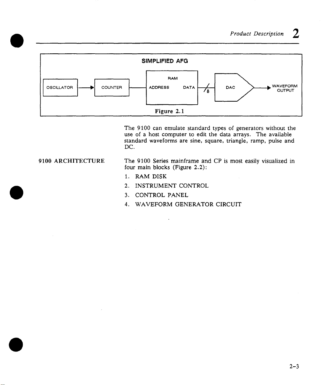
A simple way of thinking about the operation of an AFG is
shown in Figure 2.1. Basically, an oscillator clocks a counter
which in turn advances the address applied to a memory. The
memory data value which is stored in the next sequential loca-
tion is then output to the digital-to-analog converter (DAC).
Finally the DAC converts the data value to an analog level. As
the counter steps through the memory addresses, the associated
data values are converted by the DAC. This results in a voltage
waveform being output which is proportional to the data array
which resides in the memory.
Page 13
COUNTER
Product Description 2
SIMPLIFIED AFG
RAM
ADDRESS DATA
DAC
~
Figure 2.1
The 9100 can emulate standard types of generators without the
use of a host computer to edit the data arrays. The available
standard waveforms are sine, square, triangle, ramp, pulse and
DC.
WAVEFORM
OUTPUT
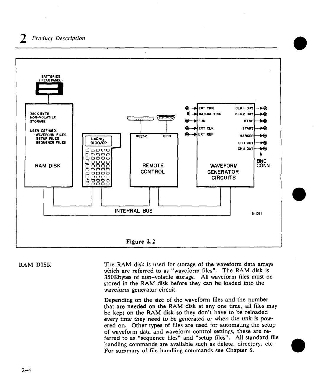
9100 ARCHITECTURE
The 9100 Series mainframe and CP is most easily visualized in
four main blocks (Figure 2.2):
1. RAM DISK
2. INSTRUMENT CONTROL
3. CONTROL PANEL
4. WAVEFORM GENERATOR CIRCUIT
2-3
Page 14
Product Description
BATTERIES
( REAR PANEL)
35OK BYTE
NON’VOLATILE
STORAGE
USER DEFINED:
¯ WAVEFORM FILES
SETUP FILES
SEQUENCE FILES
RAM DISK
RAM DISK
LeCroy
91001CP
r-, CI D I~ I’~
0 rZ_, 0 ,D ,_-I
, ~ I:l i’ll_ I=l 1:7
:
i_~ ,~ ~_ ~_ ,-,
,..~ I-, O. Ci ,-,
1
The RAM disk is used for storage of the waveform data arrays
which are referred to as "waveform files". The RAM disk is
350Kbytes of non-volatile storage. All waveform files must be
stored in the RAM disk before they (~an be loaded into the
waveform generator circuit.
~........................../
1
RS232 GPIS
REMOTE
CONTROL
INTERNAL BUS
Figure 2.2
EXT TRIG
MANUAL TRIG
SUM
EXT CLK
EXT REF
WAVEFORM
GENERATOR
CIRCUITS
CLK I OUT
CLK2 OUT
8YNC
START
MARKER
CH I OU1
CH 2 OUT
BNC
CONN
B-IOI I
2-4
Depending on the size of the waveform files and the number
that are needed on the RAM disk at any one time, all files may
be kept on the RAM disk so they don’t have to be reloaded
every time they need to be generated or when the unit is pow-
ered on. Other types of files are used for automating the setup
of waveform data and waveform control settings, these are re-
ferred to as "sequence files" and "setup files". All standard file
handling commands are available such as delete, directory, etc.
For summary of file handling commands see Chapter 5,
Page 15
Product Description 2
INSTRUMENT CONTROL
CONTROL PANEL
WAVEFORM
GENERATOR CIRCUIT
All functions of the instrument are accessible remotely via either
GPIB or RS-232. All details of operation over GPIB are located in Chapter 5 of this manual. The command syntax and
operation over GPIB and RS-232 are identical with a few exceptions outlined in the section covering RS-232.
Once arbitrary waveform files are transferred into the RAM disk
via the GPIB interface or the RS-232, all other operations can
be controlled locally from the control panel. This includes loading waveforms from the RAM disk into the Waveform Generat-
ing Circuit, setting all waveform attributes and executing "sequence files" and "setup files" as well as accessing status sum-
maries. Operation of all standard functions are supported via
the 9100/CP control panel. For complete instructions on operating via the control panel refer to Chapter 4.
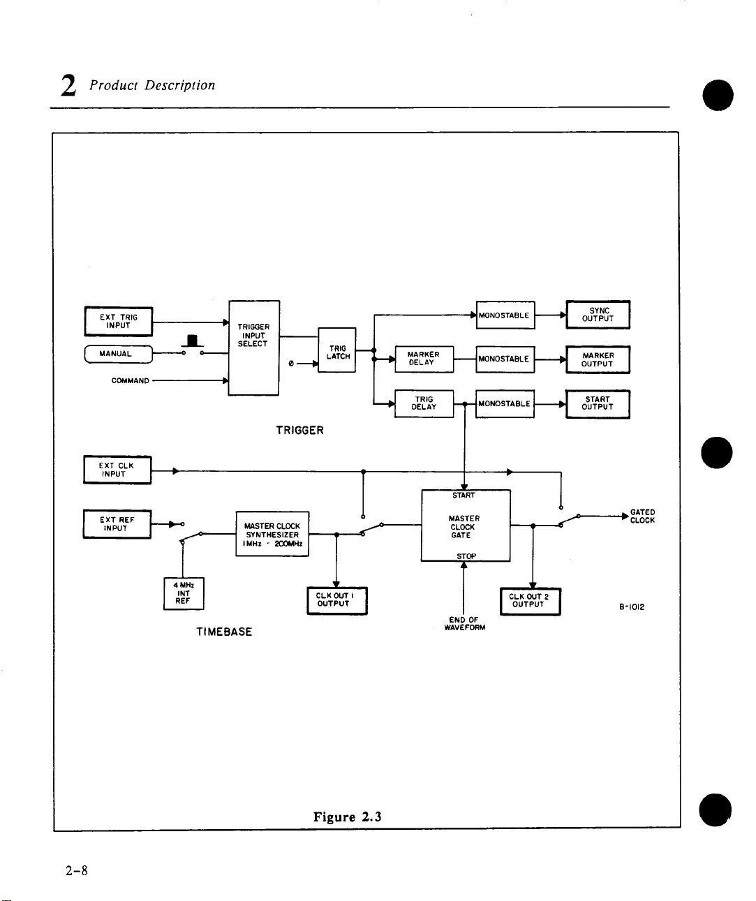
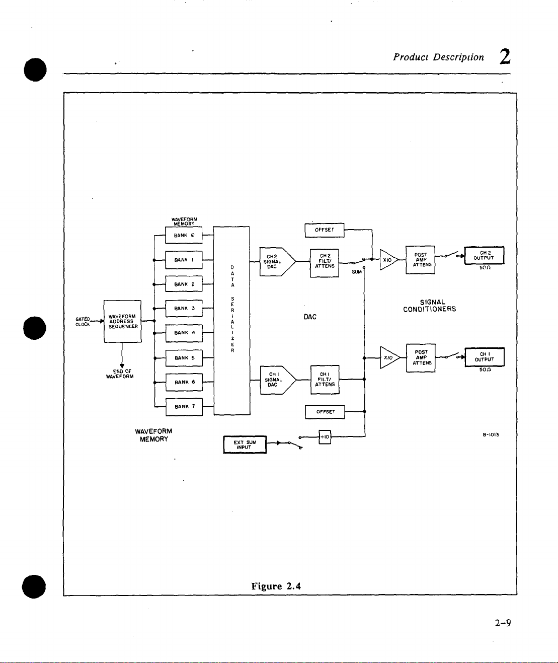
This is the block which takes the waveform files and converts
them into an analog waveform. Brief block diagrams are shown
in Figures 2.3 and 2.4. The five main subcircuits are the trigger, time base, waveform memory, digital-to-analog converter,
and signal conditioner.
An understanding of some of the internal architecture will help
explain the response of the analog output to various combina-
tions of output amplitude and offset while in different operating
modes.
Refer to the signal conditioning section of Figure 2.4. Under
ideal circumstances the 9100 will choose the post-amplifier attenuators to achieve the requested amplitude. This allows the am-
plifier to produce large swings. The post amp attenuators attenu-
ate all three aspects of the signal: the signal itself, the offset and
any background noise. To offer extra versatility, there are pre-
amplifier attenuators which may be selected in lieu of or in addition to the post-amplifier attenuators. The preamplifier atte-
nuators attenuate only the signal; any offset or background noise
of the amplifier is not attenuated. When using the preamplifier
attenuators to accommodate large offsets, the apparent Signalto-Noise ratio of the output may decrease slightly.
Amplitude always refers to the peak-to-peak swing at the output
for a digital change of 255 counts in a waveform field. Offset is
the voltage level that will be output when a digital value equal to
the ZREF level is generated by a waveform file. In the following
text ideal calibration of the analog circuits is assumed. In actual
9100 units, the internal calibration will create transitional points
which may differ from the exact values discussed below. This is
normal.
2-5
Page 16

Product Description
If there is a conflict in requested amplitude and offset settings,
the 9100 always tries to achieve the requested amplitude in pref-
erence to the requested offset. A general guideline relating
maximum offset to requested amplitude is that you can always
achieve an offset of between 8 and 16 times the requested amplitude as long as all points of the waveform are within the
4-5 V limitation (assuming a 50 12 load) of the output amplifier.
To calculate the exact value of maximum offset achievable for a
given amplitude you first divide the requested amplitude into
10 V. This gives you the total attenuation factor that is re-
quired. If this value is less than 32 then the achievable output
levels will be anywhere within the 4-5 V range. For attenuation
factors greater than or equal to 32, divide the required attenu-
ation factor by 32 and choose the next higher power of 2 than
the result. For example, if the division yields a result of 11.32
the next higher power of 2 would be 16. This power of 2 is the
least amount of post-amplifier that will be utilized up to a maxi-
mum of 64 (2^6). The maximum achievable output level
4-5 V divided by post-amplifier attenuation.
In requesting an offset value you should be aware that any point
of the output waveform which exceeds the achievable output
levels due to the combination of amplitude, offset and ZREF
will generate an error message. A clipped or distorted output
may also result from exceeding the maximum output levels.
NOTE: The amplifier will appear to operate, with reduced performance, for levels up to 125% of the calculated maximum
levels.
When the 9100 detects an output programming which exceeds
the maximum levels an warning code of 202 is set into STB4
and bit 4 of STB7 (a warning) is set. The facts described above
can be quickly understood with the following example. Start by
generating any convenient waveform with the 9100 and set the
offset to 4.8 V and ZREF to 127.5. Set the amplitude to 10 V.
Clearly the top half of the waveform is cutoff or clipped due to
the limitation of the amplifier and an error message has been
generated. Reduce the amplitude to 1 V. The output will appear
correct since the amplifier has some usable range beyond the
5 V limitation described above, but an error message will again
be generated. Further reduce the amplitude to 330 inV. At this
point the offset to amplitude ratio is near the maximum achiev-
able value of 16.
A reduction in the requested amplitude to 300 mV requires additional post-amplifier attenuation. As a result, the 300 mV am-
plitude request will allow for only a 2.5 V offset even though
the unit has been requested to generate a 4.8 V offset. An error
2-6
Page 17
Product Description 2
"
message will be generated. Also at this point the amplifier is
being driven well above its 25% safety margin and the output is
fully saturated; no visible signal appears, only insufficient offset
is perceived. The unit will not indicate the erroneous offset
value if queried, but instead returns the requested offset value.
If the requested amplitude is changed back to 330 mV, then the
9100 will again generate 4.8 V of offset. As a final example, if
the requested amplitude is 40 mV, then the maximum achievable offset is 625 mV.
Similar concerns apply to attenuator selection when sum modes
are utilized. When external sum mode is selected, the sum signal is injected at the input of the output amplifier. To avoid
attenuating the external sum signal, the 9100 chooses to use the
preamplifier attenuators in preference to the post-amplifier atte-
nuators. This tends to cause a slight reduction in signal-to-noise
ratio. However, when the requested amplitude for the internal
generated signal is less than 312 mV, some post-amplifier atte-
nuators are required. This causes the external portion of the
summed signal to be attenuated.
NOTE: No error message is generated.
The 312 mV comes from the fact that the pre-amp attenuators
offer an attenuation factor of 16 and the fine gain control of
the Signal DAC offers a factor of 2 for a total attenuation of 32
without using the post-amplifier attenuators. 10 V divided by 32
equals 312.5 mV.
When the two channels are summed, the summing is dgne at
the preamplifier point of the circuit. To be certain that the cor-
rect gain will be applied to each channel’s contribution to the
summed’ signal you should verify that both channels’ amplitudes
can be generated with the same amount of post-amplifier attenuation. This typically limits the ratio of the two channels’
amplitudes to a value between 16 and 32. A safe method is to
limit the ratio of the two channels’ amplitudes to less than or
equal to 16. If this is not done, then the amplitude contribution
of the lower amplitude channel will be greater than pro-
grammed.
2-7
Page 18
Product Description
EXT TRIG
I
INPUT
(MANUAL
EXT CLK I
INPUT
tN PUT
COMMAND
~
I
_1__
oo
~..
I INPUT ~ I
sELEcT
I
, [ TRIG I z
TRIGGER
MASTER CLOCK
SYNTHESIZER -’
IMHz - 20OMHz
I 1
TI MEBASE
i
~
I CLKOUT, I
I O~TPOT I
~H ~1
OUTPUT
/
~~
START
MASTER
CLOCK
GATE
STOP
T
END OF
WAVEFORM
CLK OUT 2
OUTPUT I
I
OUTPUT
]
1
GATED
v CLOCK
B-IOI2
2-8
Figure 2.3
Page 19
Product Description 2
Figure 2.4
2-9
Page 20
Product Description
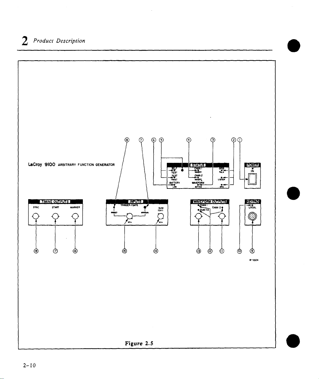
LaCroy 9100 ARBITRARY FUNCTION GENERATOR
2-10
"
II
HAN I CHAN
¯ UM 1"2
I I Ill
B-1004
Figure 2.5
Page 21
FRONT PANEL CONTROLS,
CONNECTIONS AND
INDICATORS
Product Description 2
[] Power Switch Rocker switch that turns AC power on or off.
LED above switch indicates power is on.
[] Manual Trigger Pushbutton: Will cause a single shot trig-
ger when pressed, if it is enabled via trigger source selection. If
held down it will cause continuous triggers at a rate of about 2
per second.
[] Armed LED: Indicates trigger is armed, that is, if a trigger
is received on an enabled trigger source the waveform will be
output. Meaningful only if 9100 is "in a triggered mode (not
free-running) and a waveform is active.
[] GPIB Status LED’s
STATUS LED’s
[] Waveform Output Status LED’s
Talk: Indicates 9100 is currently addressed to talk.
Listen: Indicates 9100 is currently addressed to listen.
SRQ: Indicates 9100 is asserting SERVICE REQUEST.
[] Waveform Active LED: When lit, indicates waveform is
loaded and running.
[] CHAN 1 or CHAN 2 invert LED’s: The waveform for the
indicated channel is inverted if one of these is lit.
[] Self-Test Controls: The self-test is performed automatically
on power-up, and can be invoked at any other time by pressing
the pushbutton to the right of the self-test LED. The self-test
LED is lit when the Model 9100 is performing the self-test. If
the self-test procedure identifies a fault the test-fault LED will
flash temporarily. If the test fault LED is lit steadily, it indicates that the 9100’s CPU has stopped functioning.
[] Battery Low LED: Indicates when the RAM disk back-up
battery is low. When this LED is lit, the batteries should be replaced by an equivalent pair of 3 V lithium cells.
[] Local LED: When lit means the 9100 is being controlled
via the 9100/CP control panel or RS-232. When off, the 9100
is capable of responding to commands from GPIB. The 9100 is
in the local state on power-up.
CHAN 1: Indicates waveform being output on Channel 1. When
blinking an overload has occurred. The overload can be cleared
by enabling the channel’s output.
CHAN 2: Indicates waveform being output on Channel 2. When
2-11
Page 22
Product Description
blinking an overload has occurred.
SUM 1+2: Indicates that the 2 channels of a dual waveform are
being summed and output on Channel 1 output. A flashing indi-
cation is caused by an overload on the External Sum input. An
overload can be cleared by reasserting the Sum On command.
Input/Output Connectors
[] Keypad Connector: The cable from the 9100/CP plugs into
this connector.
[] CHAN 1 Waveform Output: BNC connector for Channel 1
output. Active when either CHAN 1 LED or SUM 1+2 LED is
lit.
[] CHAN 2 Waveform Output: BNC connector for Channel 2
output. Only active when the CHAN 2 LED is lit.
[] SUM(CH 1): Input connector for summing an external
analog signal in with the signal being generated on Channel 1.
The external sum input must be enabled using the XSUM command or selection on the 9100/CP.
[] TRIGGER/GATE: External trigger or gate input connector.
Acts as trigger or gate input depending on trigger mode selected.
[] MARKER: Timing pulse which can be programmed to be
output in the range from 2 to 1 million clock cycles after receipt
of trigger. The marker output is functional only in Single, Burst,
or Recurrent trigger modes. Note that if the Marker delay is
programmed for a number greater than the sum of the trigger
delay and the total number of points that will be output (includ-
ing segment repetitions, links, and waveform repetitions), no
Marker pulse will be generated. Also, at clock rates greater than
10 MHz, the width of the Marker pulse (nominally 100 nsec)
may be reduced if it is positioned within 100 nsec of the last
point generated.
2-12
[] START: Timing pulse which is output at the beginning of
each iteration of the waveform.
[] SYNC: Is a pulse that occurs approximately 2 clock cycles
after receipt of trigger and is synchronized to the selected clock
source.
Page 23
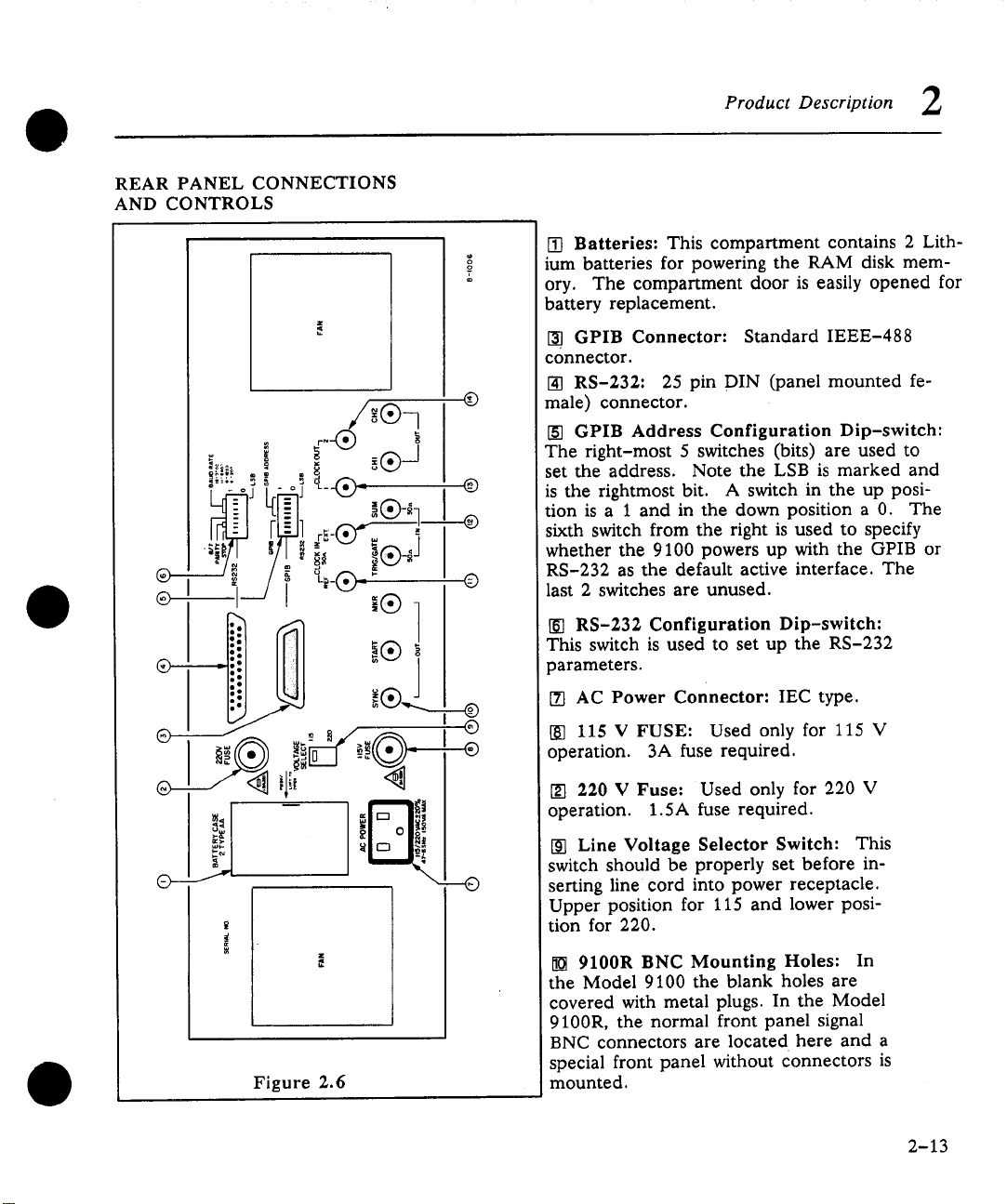
REAR PANEL CONNECTIONS
AND CONTROLS
Product Description 2
[] Batteries: This compartment contains 2 Lith-
ium batteries for powering the RAM disk memory. The compartment door is easily opened for
battery replacement.
[] GPIB Connector: Standard IEEE-488
connector.
[] RS-232: 25 pin DIN (panel mounted fe-
male) connector.
[] GPIB Address Configuration Dip-switch:
The right-most 5 switches (bits) are used
set the address. Note the LSB is marked and
is the rightmost bit. A switch in the up posi-
tion is a I and in the down position a 0. The
sixth switch from the right is used to specify
whether the 9100 powers up with the GPIB or
RS-232 as the default active interface. The
last 2 switches are unused.
[] RS-232 Configuration Dip-switch:
This switch is used to set up the RS-232
parameters.
[] AC Power Connector: IEC type.
Figure 2.6
@
[] 115 V FUSE: Used only for 115 V
operation. 3A fuse required.
[] 220 V Fuse: Used only for 220 V
operation. 1.5A fuse required.
[] Line Voltage Selector Switch: This
switch should be properly set before in-
serting line cord into power receptacle.
Upper position for 115 and lower posi-
tion for 220.
[] 9100R BNC Mounting Holes: In
the Model 9100 the blank holes are
covered with metal plugs. In the Model
9100R, the normal front panel signal
BNC connectors are located here and a
special front panel without connectors is
mounted.
2-13
Page 24
Product Description
[] CLOCK IN REF: A 4 MHz reference oscillator, amplitude
between 1 and 4 V p-p, may be used as the 9100 reference
oscillator instead of the internal crystal. It is input here and the
signal is AC coupled.
[] CLOCK IN EXT: The internal synthesizer may
be bypassed altogether and the 9100 can be driven by a clock
signal that is input to this connector. This input is selected via
the CLOCK SOURCE command.
m
[] CLOCK OUT 1: Ungated clock output at the point rate for
single channel waveforms, or twice the point rate for dual channel waveforms.
[] CLOCK OUT 2: Gated clock output for master-slave op-
eration.
2-14
Page 25
SPECIFICATIONS
WAVEFORM OUTPUTS Channels: 2
D.C. Accura.cy: 1.0% of level or 1.0% of Full Scale amplitude
or 20 mV (whichever is greater).
Resolution: 8 bits (256 levels).
Dynamic Range: Single or dual channel - 8 bits; Channels
summed - 9 or more bits, depending on wave shape, filtering,
offset requirements.
Total Harmonic Distortion: < -50 dBc for output frequency of
1 MHz or less. < -35 dBc @ 10 MHz, Typically < -38 dBc @
10 MHz for output levels < 5V p p
Spurious and non-harmonic distortion:
Intermodulation distortion: Two tone intermodulation (CHI:
10 MHz, 1 V p-p; CH2:10.25 MHz, 1 Vp p, summed
mode) typical -58 dBc 3rd order; -70 dBc 5th order.
Signal to Noise Ratio:
Full Scale Amplitude
75 mV or greater
30 mV
5 mV 25 dB
S/N specified at 0 V offset, sum mode off.
Maximum Output Voltage: 10 V p-p (4- 5 V) into 50 11,
V p-p into high impedance.
Minimum Output Voltage: 5 mV p-p into 50 fl.
Risetime: <5 nsec, 10% to 90% (no filter)
Overshoot and Ringing: 5% of p-p amplitude, maximum; 3%
of p-p amplitude, typical
Settling Time: 20 nsec to 3% for 5 V transition, including
risetime (filters off).
Offset: Individually programmable for each channel.
Offset Resolution: < 6 mV steps
Offset Accuracy: Same as D.C. accuracy
Product Description 2
<-65 dBc, f < 1 MHz
<-60 dBc, f > 1 MHz
excluding the band within
1 kHz of carrier.
S/N
~45 dB
40 dB
2-15
Page 26
Product Description
STANDARD FUNCTIONS
(WAVEFORMS)
Maximum Offset Voltage:
External Load: Max. Offset V:
50 n 4-5 V
Open Circuit 4-10 V
Output Smoothing: Built-in filters with programmable cutoff
frequencies: bypassed, 1, 3, 10, 30, 100 MHz; 18 riB/octave
(Bessel)
Crosstalk between channels: < I%
Ch I to Ch 2 Phase Accuracy:
Sinewave - Frequency Range: 0.01 Hz to 25 MHz
Frequency Resolution: 0.035%
Squarewave - Frequency Range: 0.01 Hz to 100 MHz
(50 MHz dual channel)
Frequency Resolution: 0.035%
Triangle -
Pulse - (single channel only) Period: 40 nsec to 10 sec; Width:
variable, 5 nsec to 10 sec (not to exceed period); Orientation:
selectable, positive or negative going.
Ramp - Period: 40 nsec to 100 sec; Resolution: 0.035%;
Linearity:--1-1%; Orientation: selectable, positive or negative going.
DC - Generates a D.C. level, the value of which is the offset
level. Accuracy: the greater of 1% or 20 mV.
Frequency Range: 0.01 Hz to 25MHz
Frequency Resolution: 0.035%
Linearity: 4-1%
Internal Summing -I-.5 nsec
Dual Outputs 4-1 nsec
TIME BASE (Clock Rate)
TRIGGER
Modes
2-16
Range: 5 nsec to 20 sec per point
Resolution: 0.035%
Accuracy: 5 ppm, at achievable set points, 230 C,
115 VAC/60 Hz, after 30 minute warmup
Stability: < 0.5 ppm/° C
Continuous: The generator runs continuously at the selected
frequency.
Page 27
Product Description 2
Recurrent: The waveform is cycled with a programmable delay
of up to 1 million points (1/2 million in dual channel) between
cycles. Number of waveforms per cycle is programmable up to
65,535.
Single: Upon receipt of a trigger, the selected waveform is generated only once. The start of the waveform can be delayed
from the trigger point by up to 1 million points (1/2 million in
dual channel).
Burst: Upon receipt of a trigger, the selected waveform is generated the number of times set into the burst counter, up to
65,535. The start of the burst can be delayed up to 1 million
points (1/2 million in dual channel).
Gated (uses the trigger threshold): Uses a triggered start and
stops at the completion of the current waveform cycle after the
gate closes.
External Trigger Threshold:
Source
Arm Source:
WAVEFORM MEMORY
Slope + or Range-4-2.5 V
Resolution 20 mV (8 bits)
Manual
External
Bus
Auto - Automatically rearms itself.
Bus - Rearmed from the GPIB, RS-232 or the
Control Panel.
Trigger sources and arm sources may be individually enabled or
disabled.Internal triggering is automatically selected in continuous or recurrent trigger modes
Delay: Variable, from four to one million points (2 to 1/2 million in dual channel).
Fast Memory Length: Single Channel - 64 Kpoints; Dual
Channel - 32 kpoints each channel.
Storage Memory Length (RAM Disk): > 350 Kpoints for
waveforms, setup and sequence files.
RAM Disk to Fast Memory Load Rate: 250 msec +0.7 l~sec/
byte.
Front-panel button
External trigger applied via a front panel BNC
Trigger from GPIB, RS-232 or Control Panel
Control Panel Trigger Key
2-17
Page 28
Product Description
Battery back-up:>3 years (non-rechargable Lithium cells).
Minimum Waveform Length: Nonlinked waveform segment, no
looping - 8 points (4 points for each channel in dual mode);
linked waveforms - Single channel operation - 72 points, Dual
channel operation - 36 points for each channel.
Waveform Length Resolution: Single channel operation - 8
point blocks, Dual channel operation - 4 point blocks.
Waveform Loop Counter: One counter per linked waveform
maximum repetitions - 4095.
OUTPUTS:
Front Panel:
Rear Panel:
INPUTS
Front Panel
Protection: Waveform outputs are protected against applied
voltages to 4-40 V. If an externally applied overvoltage condition is detected, the output relay is opened, the LED for that
channel is flashed and, if enabled, an SRQ is generated on the
GPIB. The condition can be cleared by reconnecting the channel’s output.
Waveform Outputs - Output impedance, 50 12; All Timing
Outputs - Output impedance, 50 12, source 1.5 V peak into
50 12, approximately 75 nsec duration.
Time Marker Output - Settable from two up to one million
clock cycles, referenced to the trigger point.
Sync Output - Occurs at the next Sample Clock edge after
receiving a trigger.
Waveform Start Output - Occurs at the start of the waveform.
Clock Outputs - 0 to -0.8 V into 50 12. Approximately a
square wave. Present in all modes including External Clock.
Protection: The maximum input voltage level for all inputs
should not exceed 5 V.
External Gate/Trigger Input - Impedance: 50 12
Sum Input - Impedance: 50 12. Overload is indicated by flash-
ing Sum 1 + 2 LED. Gain: X 1, 4-5% for >350 mV full scale
output ranges. Bandwidth: >80 MHz at 3 dB
Hand-Held Keypad (Control Panel) Input - DIN connector is provided for attaching the hand-held control panel and
display.
Rear Panel
2-18
External Clock Input - When this input is selected, the inter-
nal clock is deselected and the waveform is generated using the
Page 29

Product Description 2
external clock. Impedance: 50 12 Threshold: Variable -4-2.5 V,
8 bits resolution.
External Reference Input: Selection of this input causes the
internal clock to phase lock to it. It requires a 4 MHz signal
with 1 to 4 V p-p amplitude into 50 12, AC coupled.
2-19
Page 30
Product Description
FRONT-PANEL
INDICATORS AND
CONTROLS
Controls
Indicators
Power ON/OFF
Manual Trigger Button
Manual Self Test Button
Hand-held Control Panel (optional)
Power on LED - ON when power is applied to the instrument.
Trigger Armed LED - ON when awaiting a trigger signal.
Waveform Output LED’s: Chan 1: ON when Channel 1 is
turned on; Chan 1 & 2: ON when Channel 1 is being summed
with channel 2. Chan 2: ON when Channel 2 is turned on.
Waveform Active LED: ON when a waveform is being clocked
out of the fast memory to one or both waveform outputs or if
the unit is armed and waiting for a trigger.
GPIB: Talk LED - ON when the instrument is in the talk
mode.
Listen LED - ON when the instrument is in the listen
mode.
SRQ LED - ON when the SRQ line is asserted and the
instrument is awaiting action from a GPIB controller.
Remote - This word is spelled out in the hand-held
control panel display whenever the instrument is put into
remote by a GPIB controller.
Local LED - Located with the keypad input connector,
it indicates when the instrument is in the LOCAL mode
and the hand-held control panel is operative. When it
is not ON, the instrument is in the GPIB remote state.
Self Test LED - ON when a self test or calibrate is in progress.
Test Fault LED - Flashes for 10 seconds when a self test or
calibrate determines there is a fault or steady ON in the event
of a microprocessor failure.
Battery Low LED - ON when the RAM Disk memory backup
battery is too low.
Chan 1, Invert LED - ON when Ch 1 output is inverted.
Chan 2, Invert LED - ON when Ch 2 output is inverted.
2-20
Page 31

REAR PANEL
CONNECTORS AND
SWITCHES
WAVEFORM CREATION
AND EDITING
A
Product Description 2
Connectors: GPIB: IEEE 488-1978 compatible; RS-232 Port:
DB 25 S Connector.
Switches: GPIB Address Switch; RS-232 Port Configuration
Switch, Line voltage selector and fuses.
LeCroy’s EASYWAVE® software package is available for PCDOS compatible computers*. It provides for waveform creation
and editing in a menu driven environment. Waveform creation
can be accomplished by any of the following methods:
1. Equation entry.
2. Selecting and combining simple waveform elements.
3. Waveforms can be acquired over the GPIB from
LeCroy Oscilloscopes and then edited.
Editing may be accomplished as follows:
1. Modifying individual points from the keyboard.
2. Modifying the equation describing the waveform.
3. Deleting, moving and rescaling blocks of data.
* Minimum hardware configuration of host computer 640K
RAM, 10 Mbyte Hard Disk, Graphics (CGA,HGA, or EGA)
Display.
Other GPIB Compatible Controllers: Waveforms can be created and edited on other controllers using user supplied software.
INSTRUMENT CONTROL
GENERAL
PC-DOS Compatibles: The same software package used for
waveform editing also can be used for controlling the 9100.
Local Control Panel: Once the waveforms have been loaded to
RAM Disk, an optional, detachable control panel with a four
line LCD display may be used for controlling the 9100.
Other GPIB or RS-232 Compatible Controllers: Other com-
puters or terminals may be used to control the instrument using
the remote commands.
GPIB Interface Functions: IEEE 488-1978 compatible. SH1,
AH1, T5, TE0, L3, LEO, SR1, RL1, PP0, DC1, DT1, CO
GPIB DMA Rates: Typically >__200 kbytes/sec
RS-232C: Implemented as data communications Equipment
(DCE).
2-21
Page 32

Product Description
Baud Rates: 300, 600, 1200, 2400, 4800, and 9600.
Data Bits: 7 or 8.
Stop Bits: 1 or 2.
Parity: None, Even, or Odd.
Protocol: Full Duplex, Xon/Xoff (DC1/DC3) handshake,
Data Formats: #I Arbitrary length ASCII #L ASCII HEX "00"
to "FF" (double the length of internally stored binary data files)
Commands: Full Conversational same as GPIB plus: RS_SRQ,
Define character equivalent to SRQ in GPIB. Default is "Bell",
ESC commands ECHO on/off Trig remote/local
Temperature Range: 15o C. to 35o C., full specification; 0° C.
to 40o C., operating.
Humidity: 40o C., 10% to 95% relative, non-condensing.
Power: 115/220 +/- 20% VAC,47-63 Hz. approximately
147 watts
Size: 5-1/4" H X 19" W X 15" D.
Weight: 26 lbs. (approximately).
STANDARD ACCESSORIES I each Operator’s Manual
r
ORDERING INFORMATION 9100
9100R
9101
9109
OPTIONAL ACCESSORIES
EASYWAVE® is a trademark of LeCroy Corp
IBM XT/AT® is a registered trademark of International Business
Machines Corp
2-22
9100/CP
9100/EC
9100/OM
9100/SM
9100/SW
9100/SP
9100/MM
9100/MM1
9100/MM2
9100/RT
9100 GPIB2
DC/GPIB-2
Dual Channel Arbitrary Function Generator
Dual Channel Arbitrary Function Generator with
Rear Panel Connectors
Single Channel Arbitrary Function GeneratOr
Dual Channel Arbitrary Function Generator with
Digital Word Outputs
Detachable Hand-held Control Panel
6’ Extender Cable (Control Panel)
Operator’s Manual
Service Manual
EASYWAVE Software
Advanced Waveform Creation Software
Waveform Memory Expansion - 1/2 Mbyte
Waveform Memory Expansion - 1 Mbyte
Waveform Memory Expansion - 2 Mbyte
Real-Time Waveform Selection
GPIB Interface Card and Software (National
Instruments PCII Card and GPIB-PC Software)
GPIB Cable, 2 meters
Page 33

3
PREPARATION FOR USE
OPERATING
ENVIRONMENT
Voltage Selection and
Fuse Check
[OPERATIONS
The Model 9100 should be operated only within the following
environmental limits:
Temperature: 15°C to 35° C, in spec;
0°C to 40° C, in operating.
Humidity: 40° C, 10% to 95% relative, non-condensing.
Specifications are rated from +15° C to +35° C.
The Model 9100 has been designed to operate from either a
115 V or 220 V nominal power source. On the rear panel of
the instrument, a switch permits user selection of either voltage.
Also on the rear panel, separate fuses are provided for each
voltage.
Prior to powering up the Model 9100, make certain that the
voltage selector switch is set to whichever of those two voltages
corresponds to the available power supply and that the fuse for
that voltage is intact and properly installed.
CAUTION: The Model 9100 will fail to operate and could be
damaged if plugged into a voltage other than that which the
voltage selector switch on the rear panel is set. Thus, correct
line voltage selection MUST be made before plugging the
instrument in or turning it on.
Power Cable
GPIB Address Selection
The Model 9100 has been designed to operate from a
single-phase power source with one of the current-carrying
conductors (neutral conductor) at ground (earth) potential.
Operation from power sources in which both current-carrying
conductors are live with respect to ground (such as
phase-to-phase on a tri-phase system) is not recommended.
The instrument is provided with a three-wire electrical cable
containing a three-terminal polarized plug for line voltage and
safety ground connection. The plug’s ground terminal is
connected directly to the frame of the unit. For adequate
protection against electrical hazard, this plug must be inserted
into a mating outlet containing a safety ground contact.
The Model 9100’s 8-segment GPIB address switch is located on
the instrument’s rear panel. Segments 1 and 2 are unused.
Segment 3 selects the communication source. A "1" selects
GPIB and "0" selects RS-232.
3-1
Page 34

Operations
Segments 4 through 8 on the switch are used for GPIB address
selection as shown in Figure 3.1.
1 = GPIB, 0 = RS-232
GPIB Address
¯
O OOOOOO 0 o
r
16 8 4 2 1 Binary Equivalent
For Example:
0 0 0 0 0 = 0
0 0 0 0 1 = 1 The default address
1 0 0 0 1 = 17 Typical Address
1 1 1 1 1 = 31 automatically defaults to 1
Valid Addresses are 1 through 30
Not a valid address
automatically defaults to 1
Not a valid address
RS-232 Switch Setup
Power-On Procedure
3-2
Figure 3.1
GPIB Selection and Addresses
Refer to Chapter 6.
As described in the preceding sections, the first steps in
operating the Model 9100 is to be sure that it is properly
connected to line power, that it is properly fused, and that the
selector switch on the rear panel is set to the same voltage as
line power.
Once those steps are complete, press the power switch (in the
upper right corner of the front panel) to the ON position. The
LED above that switch will light to indicate that power is on.
Also on will be the SELF-TEST light in the STATUS rectangle
to the left of the power switch. This light indicates that the
instrument is undergoing calibration, which is part of self-test.
When the calibration is complete the self-test LED will no
longer be lit.
Page 35

Operations
NOTE: It is normal for all front-panel lights to flash on prior
to self-test.
After calibration, the instrument initializes all control settings,
which takes several seconds. During this time the LOCAL LED
will be on. The remote interfaces are ignored until initialization
is complete, to avoid any possible conflicts. After initialization
the message "LECROY 9100" appears on the 9100/CP, if it is
attached. If a GPIB controller places the instrument in the
REMOTE state during initialization, this will be recognized at
the end of initialization. If the communications source is
RS-232, a prompt "AFG\>" is sent over RS-232 at the end of
initialization.
The instrument is now ready to use in its power-up mode. All
instrument settings will be at their default values and only the
POWER and LOCAL LED’s will remain lit (the Model 9100
powers up in LOCAL mode, which means it is at that point set
to be controlled by the 9100/CP).
When settings are changed to meet the needs of specific
operations, and/or if appropriate commands are given to invoke
REMOTE (computer) control of the instrument, different
front-panel LED’s will light up accordingly.
3
OPERATING THE 9100
STANDARD FUNCTIONS
In the following sections the general format of remote
commands will be given to show how certain operations are
invoked. The argument descriptor will often be shown as the
argument name or explanation enclosed in angular brackets.
For example:
Command: CLOCK_PERIOD,<desired period>;
The type of argument is not to be entered literally when the
command is used. The angular brackets and text enclosed
should be replaced by the properly formatted argument in
accordance with the rules specified in Chapter 5. The argument
is typically a number with a unit appended to it with no
embedded spaces.
All commands except for those that transfer files into and out
of the 9100 can also be given using the 9100/CP via its
menu-driven command entry. See Chapter 4 for the 9100/CP
menu description.
Standard functions may be generated with the 9100 using the
9100/CP or by command over the bus without loading or using
any waveform files. The standard function modes completely
emulate the usual function generator operation by automatically
generating the waveforms needed in the waveform memory. In
3-3
Page 36

Operations
all these modes the user simply enters the parameters needed
(for example, frequency and phase for sine generation) and the
rest is done automatically.
The standard functions are accessed under the FUNC main
menu key on the 9100/CP. For detailed instructions on the
menu driven operation of the standard functions see Chapter 4.
To operate standard functions under remote control, first send
the command which forces the 9100 into the particular standard
function mode (a single word command which is usually the
name of the function, e.g., sine, pulse, ..) and then give the
GO command. The function will then be output. For a detailed
explanation of the operation of all related commands see
Chapter 5.
Listed below are the commands for setting up dual channel
I MHz sine waves with 20° phase difference between Channel 1
and Channel 2,
SINE;
SINE_MODE,DUAL;
SINE FREQUENCY, 1MHZ;
SINE_CH2_PHASE,20;
In standard function modes the clock is set automatically and
cannot be controlled independently as with arbitrary functions.
For this reason all clock related commands are disabled when in
a standard function mode. When using a 9100/CP, if an
external clock reference is needed in standard function mode it
must be selected when in arbitrary mode and then it will be
active when using standard functions. It cannot be selected
when in standard mode.
ARBITRARY WAVEFORMS
AND FILE CONVENTIONS
3-4
The LeCroy EASYWAVE software running on an IBM XT/AT
computer is the recommended method of creating and
transferring arbitrary waveform files to the 9100. The next
section carefully explains how to format and transfer waveform
files to the 9100, and Chapter 5 summarizes all the commands
and formats used. All arbitrary waveforms are handled as files
in the 9100. Once the files exist on the 9100 RAM disk all
control can be accomplished via the 9100/CP control panel.
All files in the AFG have an extension which is necessary and
significant. Below is a summary of the different types of files
you will encounter. The file name, represented by xxxxxxxx, is
the alphanumeric name that the user gives when creating the
file.
Page 37

Defining an Arbitrary
Waveform in Terms
of a Waveform File
Operations
xxxxxxxx.WAV - SINGLE CHANNEL WAVEFORM FILE
Contains the data to generate a single channel waveform. May
only be output on Channel 1.
xxxxxxxx.WAD - DUAL CHANNEL WAVEFORM FILE
Contains the data to generate a dual channel waveform.
xxxxxxxx.SET - SETTINGS FILE Used to automatically
establish all settings of the 9100 in conjunction with the SETUP
command. The LEARN command automatically generates a
setup file.
xxxxxxxx.SEQ - SEQUENCE FILE Used to contain a
sequence of 9100 commands that may be executed
automatically by giving the SEQUENCE command. This
command is most necessary when defining a complex waveform
using the LINK command.
Two types of waveform file formats are used by the 9100, one
for single channel waveforms and one for dual channel
waveforms. Both single channel and dual channel waveform files
contain a single sequence of bytes which define the waveform
data array to be generated. The bytes should be UNSIGNED, in
other words range from 0 to 255. In general, when you
calculate your waveform using your computer you will probably
be using floating point numbers to represent the voltage values
which you wish to generate. In order to convert these into 8-bit
waveform data values and maintain the maximum amplitude
resolution you should, in most cases, scale your waveform so
that the minimum value corresponds to 0 and your maximum
value corresponds to 255.
The basic constraints on the waveform files are:
1. The maximum number of bytes is 65536.
2. The number of bytes must be a multiple of 8. This is due to
a hardware constraint in the waveform memory.
The number of bytes must be greater than or equal to 8 for
3.
a waveform file that will not be "linked" with other
waveform files when loaded into the WAVEFORM
GENERATOR CIRCUIT from the RAM DISK. (See page
3-9, for an explanation of waveform file linking.)
4. The number of bytes must be greater than or equal to 72
for a single-channel waveform file that will be "linked" with
other single channel waveform files. Dual channel files that
are to be linked must contain at least 36 bytes per channel.
3
3-5
Page 38

Operations
TRANSFERRING WAVEFORM
DATA FILES INTO THE
AFG RAM DISK VIA GPIB
NOTE: If you are using the EASYWAVE Program to create and
NOTE: The extension on the waveform is significant and lets
the 9100 know what type of waveform will be contained in the
file. Filename represents the name by which you will refer to
5, Minimum data value is 0,
Maximum data value is 255.The single channel waveform file
simply contains a series of bytes in the exact order in which you
want them to be generated. The single channel waveform will
always be output on Channel 1. The format is given below
where the index specifies the interval (point in time) during
which that value will be generated. The waveform file contains
N data bytes.
a(1) a(2), a(3) a(4) a(5) a(6) ...........
The dual channel waveform file consists of interleaved pairs of
data values which will be routed to Channel l(a) and Channel
2(b). Below we designate bytes for Channel 1 as a and bytes for
Channel 2 as b and the index specifies the interval during which
that value will be generated starting with 1. This waveform file
contains 2N data bytes and when run will result in N points
being output on channel 1 and N points being output on
Channel 2.a(1)
a(2) b(1) b(2) a(3) a(4) b(3) a(N-1)
a(N)b(N-1)
load your waveform files, you may skip this section.
After you have defined the data array which will become your
waveform file, you need to transfer it to the 9100. We do this
with the STORE command.
First send the command to transfer the file.
For single channel waveforms: STORE filename.wav
For dual channel waveforms~ STORE filename.wad
the waveform file.
Next, send the file. The stream of bytes that you send consists
of either a single block of bytes or a series of blocks. If the file
is being sent in multiple blocks EOI must be asserted only with
the last byte of the last block to indicate the end of the file.
The waveform files may be transferred to the 9100 in either of
two block formats; binary (called #A format) or hex-ASCII
(called #L format). Each individual block consists of a block
3-6
Page 39

Operations
preamble, a count (the number of data bytes in #A and the
number of data values in the #L case). Below are the block
formats for the binary and hex ASCII file block transfers. In
the table, each row corresponds to a byte sent over the GPIB to
the 9100.
3
3-7
Page 40

Operations
FOR BINARY TRANSFER:
Byte Number
1
2
3
4
5
6
7
N+4 <data byte N> (with EOI, if last block)**
* Data byte count is an unsigned integer which in this case
equals N. It contains the number of bytes being transferred in
the block. In this binary representation there is 1 data value per
byte.
**EOI, if sent, must be sent with the last byte. EOI terminates
the file transfer. If EOI is not sent, the 9100 will accept another
block as part of the same file. The last block of a file transfer
must be sent with EOI on the last byte.
Byte Value
#
A (ASCII uppercase A)
<data byte count, most significant byte>*
<data byte count, least significant byte>*
<data byte 1>
<data byte 2>
<data byte 3>
(ASCII #)
FOR HEX ASCII TRANSFER:
3-8
Byte Number
1
2
3
4
5
6
7
8
9
10
2N+5
2N+6 <lsb hex digit of data byte N> (with EOI,
* Value count is the number of data bytes you are sending over
in this block. In this hex ascii representation there are 2 bytes
per data value.
Byte Value
#
L
<value count, 4th hex digit, most significant >*
<value count, 3rd hex digit>*
<value count, 2nd hex digit>*
<value count, ist hex digit, least significant>*
<most significant hex digit of data byte i>
<least significant hex digit of data byte i>
<most significant hex digit of data byte 2>
<least significant hex digit of data byte 2>
<msb hex digit of data byte N>
if no last block)
(ASCII .#)
(ASCII uppercase L)
Page 41

Operations
**EOI, if sent, must be sent with the last byte. EOI terminates
the file transfer. If EOI is not sent, the 9100 will accept another
block as part of the same file. The last block of a file transfer
must be sent with EOI on the last byte.
NOTE: When transferring files over the RS-232 interface, the
last byte must be followed by the character defined by
COMM RS CONF as simulting EOI; see Chapter 6.
LOADING THE WAVEFORM
FILES FROM RAM DISK
INTO THE WAVEFORM
GENERATOR CIRCUIT The simplest type of waveform that we can generate is based on
a single waveform file. To generate the waveform described by a
single waveform file, simply load it and go by issuing the
following commands:
LOAD filename.ext; GO;
Where ext is either WAV or WAD, if single or dual channel
respectively.
NOTE: The commands shown in this screen are remote
commands valid over GPIB or RS-232. All functions are also
accessible from the 9100/CP. Operation with the 9100/CP is
covered in Chapter 4.
If you are using only simple waveforms composed of single
waveform file, skip the rest of this section of the operation
procedure. The procedure for building up more complicated
waveforms which utilize the linking and looping capabilities of
the 9100 will now be described.
The waveform data memory length of the 9100 is 64 Kbytes.
This means that if you are using only a single waveform file the
upper limit on a single channel waveform is 64 Kpoints and for
a dual channel waveform is 32 Kpoints per channel. The 9100
provides a way to effectively generate much longer waveforms if
any parts of the waveform are repetitive in nature.
You may link together waveform files when loading into the
waveform memory to define what can be thought of as a
waveform program. Lets look at an example. Suppose you want
to generate the waveform shown in Figure 3.2. It consists of
several pieces each of which are repeated several times:
3
3-9
Page 42

Operations
1 sine cycle
I DC section
4 since cyles
2 DC sections
2 Gaussian pulses
6 DC sections
WA VEFORM LINKING
(SF.OJZ~.E_EU.E)
WA VEFORM
LOAD. SINE
LINK - T COMP
-"LINK - SINE
V
IF--LINK- r COMP
IIr"-LINK-aAus
I[I ILINK - T COMP
You could simply generate a single data file which contained all
the data as a single array or we provide another method which
will use less waveform memory. We may define three waveform
files as follows:
REPETITIONS
1
I
4
2
2
6
Figure 3.2
SINE L
T COMP - OV (10 POINTS)
GAU~L,_
3-10
Page 43

Operations
3
GAUS.WAV
SINE.WAV
T.WAV
We can then load the waveform using the following sequence of
commands:
LOAD SINE.WAV, 1;
LINK TCOMP.WAV, 1;
LINK SINE.WAV,4;
LINK TCOMP.WAV,2;
LINK GAUS.WAV,2;
LINK TCOMP.WAV,6;
GO; (when you want to start it running)
The load command always comes first and tells the 9100 that
we are loading a new waveform into the waveform memory. In
this waveform the 9100 will generate one repetition of
SINE.WAV, then one repetition of TCOMP.WAV, then four
repetitions of SINE.WAV, then two repetitions of
TCOMP.WAV, then two repetitions of GAUS.WAV, and finally
six repetitions of TCOMP.WAV. When the waveform is loaded
in this manner, as a multi-file waveform, the amount of
waveform data memory used is conserved since each unique file
has to reside in the waveform memory only once. Therefore,
the amount of waveform memory used by this waveform is the
sum only of the number of data values in the three files.
Main constraints in making linked waveforms:
1. Minimum size of each file must be 72 bytes, as opposed to
8 for a single file waveform.
2. A Maximum of 1 Load + 681 sequential Link commands
can be used to generate a linked waveform.
3. The maximum number for the repetition argument in the
load or link is 4095.
The LINK command also accepts an additional argument. The
purpose of this argument is to permit each trigger cause output
of different waveform segments.
The format of the command is:
LINK argl [arg2] [arg3];
where optional items are contained in brackets, and items to be
replaced are in lower case.
argl: filename to link, with extension, such as A.WAD.
arg2: Number between 1 and 4095, inclusive, representing the
segment repetition count. Default if not present is 1.
contains 1 Gaussian pulse
contains 1 cycle of a sine wave
contains a constant data array
3-11
Page 44

Operations
arg3: WAIT.
The "WAIT" argument, if present, tells the 9100 Series AFG to
wait for trigger before executing this segment. More precisely, it
tells the AFG to act as if the entire waveform ended with the
segment before this one, and this segment is the first one in the
next waveform repetition. A detailed discussion of the effect of
this argument will be found under "Specifying the Trigger
Mode", page 3-15.
3-12
Page 45

CONTROL SETTINGS
SUMMARY
(amplitude, clock ....
Operations
Specifying the 9100 control settings gives the user control over
the various waveform characteristics. All attributes can be
controlled from the Control Panel as well as by GPIB
commands. The values of the settings determine when a
particular waveform data point will be output and at what
voltage level. The settings can be grouped into the following
major categories shown below.
3
Channel Parameter Settings
Timebase Settings
Trigger Settings
Settings which control the signal conditioning applied to the
Channel 1 and Channel 2 signals.
CH1 AMPLITUDE CH2 AMPLITUDE
CH 1-OFFSET
CH1 ZERO REF
CH 1-FILTER CH2-FILTE-R
CH I_INVERT
CH1 OUTPUT
EXTERNAL SUM
SUM_MODI~
Settings that affect the main clock, which determines the data
point period (i.e., determines rate at which the waveform is
output).
CLOCK_RATE
CLOCK_PERIOD
CLOCK_SOURCE
CLOCK_REFERENCE
CLOCK_LEVEL
CLOCK_MODE
CLOCK_SLOPE
Settings that affect when and how the waveform is triggered.
TRIG_MODE
TRIGDELAY
TRIG SOURCE
m
TRIG ARM SOURCE
TRIG-SLOP-’E
TRIG LEVEL
MARKER DELAY
DELAY_I~ODE
A detailed explanation of every command is contained in the
command reference in Chapter 5.
CH2-OFFSET
CH2 ZERO REF
CH2 INVERT
CH2-OUTPUT
3-13
Page 46

Operations
SPECIFYING HOW THE
DATA VALUES ARE
CONVERTED TO
VOLTAGE LEVELS AMPLITUDE, OFFSET AND ZERO REF determine the output
voltage as a function of data point vaiue, V(n) where n is the
data point value.
NOTE: All voltages are for the output terminated in 50 £). If
the output load is a high impedance, then all voltages at the
output will be 2 × higher than set.
The AMPLITUDE command sets the full scale voltage range,
that is, the voltage swing obtained when the data point value
changes from 0 to 255. For example the commands to set both
channel amplitudes to 2.3 V would be:
CH1 AMPLITUDE 2.3V;
m
CH2 AMPLITUDE 2.3V;
ZERO REF sets the data point value whose output voltage does
not change when the amplitude is changed (think of it as the
fixed point or baseline). This is also the data point value which
when output from the AFG will correspond to the offset voltage.
This value must fall between 0 and 255 but need not be
constrained only to integer values (127.5 is a valid value and is
the default value for this parameter). The commands to set
zero_ref to 0 (for unipolar positive operation) are:
CH1 ZERO REF 0;
CH2 ZERO REF 0;
For unipolar positive operation zref is typically set to 0. For
unipolar negative operation zref is typically set to 255.
NOTE: For an autoscaled waveform (i.e., one that is
normalized so that the maximum value is 255 and minimum is
O) to be generated symmetrically about 0 V ZREF should be set
to 127.5, and the offset should be set to 0 V.
OFFSET sets the output voltage obtained when the data point
value is equal to zref. The following commands set the offset
on channel 1 to 1 V and the offset on channel 2 to 2 V.
CH1 OFFSET 1V;
CH2 OFFSET 2V;
To summarize:
V(n=zref) = Voffset
V(255) - V(0) = Vamplitude
so for a general data point value n:
V(n) = Voffset + Vamplitude*(n-zref)/255
3-14
Page 47

SPECIFYING THE TIME
PER POINT
SPECIFYING THE
TRIGGER MODE
Operations
Where
V(n) is the voltage output for data value n. n is the
waveform data value between 0 and 255. Voffset is the
programmed offset voltage. Vamplitude is the selected
amplitude voltage. Zref is the selected zero reference point.
The clock period attribute controls the amount of time each
waveform point is output.
CLOCK_PERIOD < time value with optional units>;
The TRIG_MODE specifies the overall running mode of the
waveform. The 9100 has five different trigger modes:
1. Continuous - On receipt of the GO command the generator
outputs the loaded waveform. When it reaches the end of the
waveform it immediately starts over at the beginning with no
interruption between the last point and the first point. The
generator will continue to cycle the loaded waveform until
receipt of an ABORT or STOP. A pulse will be output from the
START output at the beginning of each cycle. The SYNC and
MARKER outputs are not available in this mode.
COMMAND: TRIG MODE CONTINUOUS;
2. Single (triggered) - This is a single sweep triggered mode.
In general, for each receipt of a trigger the generator will
output one sweep of the loaded waveform.
a GO command the generator waits for an ARM command
(if ARM SOURCE=BUS) before it proceeds. Usually (and
by default) ARM SOURCE=AUTO, in which case no ARM
is needed. It the~ waits for receipt of a trigger from any
one of the enabled sources. While waiting for a trigger, the
first data point in the waveform is being output. Upon
receipt of a trigger a pulse is output from the SYNC
connector (the output is actually issued on the 2nd positive
clock edge after receipt of trigger). Then the generator waits
a programmed number of clock cycles called the
TRIG DELAY. At the end of the TRIG_DELAY a pulse is
generated at the START output on the front panel. The
generator then outputs the loaded waveform and stops
output, holding the last point if ARM SOURCE=BUS. In
this case, the output will remain at th~ last point until an
ARM command is received. After the ARM command is
detected, the output changes to the first point of the
waveform, and remains in that state until a trigger is
m
On receipt of
3
3-15
Page 48

Operations
received. If, however, ARM SOURCE=AUTO (the default
condition), the last point wilt only be held for the rearm
time, and then the output will switch back to the first point
automatically, and the unit will be ready to accept a trigger.
Command: TRIG MODE SINGLE;
3. Burst (triggered) - This is a multiple sweep triggered mode.
It operates identically to the SINGLE mode except that it will
output the programmed number of sweeps of the waveform
instead of just a single sweep.
Command: TRIG MODE BURST,<number of sweeps>;
4. Recurrent - This is basically a BURST mode with automatic
retriggering. It is a free running mode, not a triggered mode.
When the GO command is given in this mode the waveform will
be cycled until an ABORT or STOP is received. Although it is
free running it is identical in operation to the Burst mode with
two exceptions: (1) no trigger is needed to initiate the
waveform, and (2) the generator is automatically rearmed and
retriggered after every BURST of waveform sweeps.
Command: TRIG_MODE RECURRENT,<sweeps/cycle>
5. Gate - Gate is a combination of the triggered modes and the
continuous mode. The starting of the waveform is identical to
the triggered modes. The waveform then cycles in a manner
similar to Continuous. When the external GATE input becomes
inactive the generator will complete the current sweep of the
waveform, stop output, rearm and await the next transition of
the Gate input to the active state. The ARM feature is not
active (always set to ARM_SOURCE=AUTO).
Command: TRIGMODE GATE
The "WAIT"argument, if appended to a LINK command, tells
the 9100 Series AFG to wait for trigger before executing the
segment. More precisely, it tells the AFG to act as if the entire
waveform ended with the segment before this one, and this
segment is the first one in the next waveform repetition. This
provides interesting effects, depending on which trigger mode is
selected. It is meant to be used in single trigger mode. The
effects are as follows:
Trigger Mode (TMOD): Effect
Single: A new trigger is required to generate each segment (or
group of segments beginning with one) which has been linked
with "wait". For example, consider:
3-16
LOAD A.WAV,1; LINK B.WAV,2, WAIT;
LINK C.WAV,2,; LINK D.WAV, 3, WAIT;
Page 49

Operations
The first trigger will generate only A.WAV once, because
B.WAV was linked with "wait". The second trigger will generate
two repetitions of B.WAV and two repetitions of C.WAV,
because C.WAV was linked without "wait". The third trigger
will generate three repetitions of D.WAV. Each trigger generates
appropriate timing outputs: SYNC, START and MARKER, if
possible. The programmed trigger delay occurs following each
trigger.
Continuous: The generated waveform is not affected by links
with wait, since continuous mode never waits for trigger.
However, a START pulse is generated at each end-of-waveform
mark, i.e., at the beginning of each segment linked with "wait"
as well as at the beginning of the first (LOADed) segment.
Given the example above, a START pulse would be generated
at the beginning of A.WAV and at the beginning of B.WAV’s
first repetition and at the beginning of D.WAV’s first repetition.
The programmed trigger delay has no effect as usual.
Gated: In this mode, waveform generation is halted at the first
end-of-waveform after the GATE signal goes false. Each link
with "wait" introduces an end-of-waveform mark. Thus, to
continue the example above, in gate mode generation may stop
just before A.WAV (as normal), or before B.WAV’s first
repetition or before D.WAV’s first repetition, whichever comes
first after the gate goes false. When the gate goes true again,
output will begin with the appropriate segment, either A.WAV
or B.WAV or D.WAV, after the programmed trigger delay.
3
Burst: Burst is very similar to single, except single stops at every
end-of-wave, while burst counts the specified number of
end-of-waves and then stops. So, using the example from
"single" mode once gain, in TMOD BURST, 3 each trigger
would cause the 9100 to wait the programmed trigger delay and
then produce A.WAV followed by two repetitions of B.WAV,
two repetitions of C.WAV and three repetitions of D.WAV. The
three end-of-waveform marks are just before B.WAV, just
before D.WAV and just before A.WAV.
TMOD BURST, 1 is exactly equivalent to single trigger mode,
see above. An interesting mode is to give a burst count that is
neither 1 nor the number of end-of-wave markers in the
waveform. For example, TMOD BURST 2 would cause
A.WAV, B.WAV and C.WAV to be produced by the first
trigger (following GO); D.WAV and A.WAV to be produced
the second trigger; B.WAV, C.WAV and D.WAV to be
produced by the third trigger, etc.
3-17
Page 50

Operations
TIMING OUTPUT SIGNAL
RELATIONSHIPS
Recurrent: Recurrent is the same as burst, with an automatic
trigger immediately occurring whenever the system waits for
trigger.
In summary, in single trigger mode this feature permits the 9100
to produce a sequence of different waveforms in response to a
series of asynchronous external triggers, with as little as 70 nsec
delay from trigger to the next waveform. The trigger may also
be supplied by the TRIG command, but the response will be
slower. In either case, the response is much faster than could be
achieved if a sequence of LOAD and LINK commands had to
be executed to change the waveform. In other trigger modes,
other possibly useful effects are obtained.
The following description of timing relationships details the
operation of the SYNC, START and MARKER outputs, how
they relate to the waveform output(s), and how they change
with the selected triggering mode. For purposes of this
discussion, the unit of timing will be the waveform point (i.e.,
clock period), in order to provide an understanding of how the
timing of these signals may vary with the clock. At high clock
rates (in excess of 10 MHz), the signal timing may appear
somewhat different due to asynchronous (e.g., propagation)
delays. Unless otherwise noted, MARKER output timing is the
same as START output timing, but is programmed using the
MARKER DELAY command rather than the TRIGGER
DELAY command. Timing will also vary depending on whether
a single-channel or dual-channel waveform is being ger~erated.
Delay values for dual-channel operation will be given in
parentheses 0 following the single-channel value.
Single - After the GO command is issued, the first point(s)
the waveform will be present at the analog output(s). The AFG
then waits for a trigger from any enabled source. The first
trigger received will be synchronized to the generator’s internal
clock, and a SYNC pulse will be output. The actual time from
the recognition of a trigger to the SYNC output will vary from
one trigger to the next because of the synchronization process.
The START pulse occurs [TRIGGER DELAY - 2 (I)] points
after the SYNC. The synchronization delay is also included in
the TRIGGER DELAY, so that the actual time from a trigger to
the START will never be longer than the programmed delay
value, but may be shorter by I (1/2) point. In any event, the
START pulse occurs i point before the analog output(s) makes
the transition from the first point to the second. At the end of
the waveform, if the auto-arm function is enabled (the default
condition), the last point of the waveform is held for 10 (5 I/2)
3-18
Page 51

Operations
points. If bus arming is selected, then the last point is held until
9 (4 1/2) points after the arm command is received. This is the
trigger re-arm time, following which the analog output(s) returns
to the first point of the waveform and the unit awaits the next
trigger. Figure 3.4 shows an overview of single trigger mode
timing relationships. A more detailed view is shown in Figure
3.8.
Burst - Same as for single mode. See Figure 3.5.
Continuous - The SYNC and MARKER outputs are generated
once in response to the GO command. Their relationship to the
waveform output(s) is the same as in single mode. The START
pulse is actually generated near the end of any given waveform
cycle (which, given the nature of continuous operation, roughly
corresponds to the beginning of the next cycle). The absolute
timing from the START output to the first waveform point will
vary depending on the number of points contained in the
waveform file. Since the intent of the START pulse in this
mode is merely as a convenient triggering signal for an
oscilloscope, the exact timing relationship is non-critical. See
Figure 3.3.
Gated - In this mode, the GO command again puts the first
point(s) of the waveform at the analog output(s). The
and MARKER outputs are generated in response to the gate
signal’s transition from the "closed" state to the "open" state
(as determined by the TRIGGER SLOPE and TRIGGER
LEVEL settings), in the same manner as in single trigger mode.
Transitions on the analog output are delayed by TRIGGER
DELAY, as in single mode. The START pulses are generated
near the end of each cycle within the gate signal’s active interval
as in continuous mode. The number of repetitions is determined
by the duration of the true state of the gate input, and one
START pulse will occur for each repetition. The waveform will
continue to its natural completion after the gate "closes", and
the analog output(s) will make the transition from the last point
back to the first point after the trigger re-arm time of 9 (4 1/2)
points. The AFG then waits for the next transition of the gate
signal. See Figure 3.7 for an overview of timing relationships in
gate mode.
Recurrent - In recurrent mode, trigger delay is defined as the
time from the end of the natural duration of the last point of
one occurrence of the waveform (i.e., 1 clock period after the
transition to the last point) to the beginning of the natural
duration of the first point of the next occurrence (i.e., 1 cycle
before the transition to the second point). Our discussion of this
operating mode will therefore commence with the end of a
3
3-19
Page 52

Operations
waveform occurrence. The last point is held for its normal
duration plus 9 (4 i/2)) points while the trigger re-arms.
output(s) then make makes the transition to the first point. The
SYNC output occurs 15 (8) points after the transition to the last
point (i.e., 14 (’7) points after the last point’s normal duration).
The START pulse occurs TRIGGER DELAY points after the
normal duration of the last point (or TRIGGER DELAY +
points after the transition to the last point). The first point of
the waveform is held for one period after the leading edge of
the START pulse. Figure 3.6 shows an overview of recurrent
mode timing. More detail in shown in Figure 3.9.
3-20
Page 53

Operations
CONTINUOUS MODE OPERATION
This mode is used to loop on the programmed wavelorm in a continuous and uninternJptecl manner (i.e., the first point is
generated immediately after the last point. For example, this mode would be used to generate a continuous wave sine).
3
CH 1 OUTPUT
OH,,,°,,,HIO,.,OOOO..
START 0 I~’.PU.T .............. ~.
SYNC OUTPUT
MARKER OUTPUT
NOT USED IN CONTINUOUS
NOT USED IN CONTINUOUS
Figure 3.3
3-21
Page 54

Operations
In this mode each trigger causes a single repetition of the programmed wavelorm to be generated. Initial and final output
TRIGGERED SINGLE MODE OPERATION
levels are set by first and tast points of waveform resr~ively,
i
CH 1 OUTPUT
WAILING FOR TRIGGER
HOLDING FF~’I POINI J .............................................................
~
WAVff--I~M
w.,~ ~ ARM ~ .OMM’ANO
!HQ,I~NG LAS’T POIN IN WAVE
i
i AUTO ARM
ff____~ COMMAND
Js/~
~ WAITING FORIRI~ER
TRIGGER INPUT
SYNC OUTPUT:: N
START OUTPUT
i
i
MARKER OUTPUT :
i
3-22
Figure 3.4
Page 55

Operations
TRIGGERED BURST MODE OPERATION
In this mode each trigger causes a set number of repetitions of the programmed waveform to be generated (3 in the example
below), initial and final output levels are set by first and last points of waveform respectively.
CH 1 OUTPUT
WANING FOR Ir’dGGER
HOLD FIF¢S’[ POINT
IN WAVE
:
.
3 CYCLES OF Pf’~X;PAMMGD WAVE FOI’~V,S
3
TRIGGER INPUT
SYNC OUTPUT
START OUTPUT
MARKER OUTPUT
n
:1-1
, n
MARKER DELAY
Figure 3.5
3-23
Page 56

Operations
RECURRENT MODE OPERATION
A free running auto-triggered mode. The end of one cycle of the programmed waveform synchronously triggers the next
cycle. In this mode, a programmable trigger delay separates the cycles. By changing the trigger delay the rop rate can be
varied independent of the clock rate thus keeping the shape constant. Note that the trigger delay time includes the auto arm
interval, All timing outputs are available in this mode,
°.1o~,~ .....
..... __n ~ ~ n .....
START OUTPUT .....
MARKER OUTPUT
..... F1
] xtl~i /I
~</ ~</ ,1-1,//1 .....
I
I i
i
n
J
!
i
i
!
n
i
n
3-24
Figure 3.6
Page 57

Operations
3
GATED MODE OPERATION
Program waveform to output continuously while the gate is active. After gate becomes inactive the current cycle of the wave-
form is completed and the trigger is ready to be re-armed. TypicaUy the trigger delay should be set to minimum, but is pro-
grammable for additional flexibility.
CH 1 OUTPUT
WAITING FOR TRIGGER
HOLD FIRST POINT
IN WAVE
! DELAY (USUALLY MINIMUM)
GATE = FALSE
WAmNGFOR
GATE
GATE INPUT
SYNC OUTPUT fl
START OUTPUT
MARKER OUTPUT
MARKER DELAY
Figure 3.7
3-25
Page 58

Operations
9100 SINGLE MODE TIMING
CH1 OUTPUT
SYNC
START
RE-ARM TIME
SINGLE = 10
DUAL = 5-1/2
WAIT FOR TRIGGER
l..._5
5
I
[ I
I
I
MINIMUM PROGRAMMABLE TRIGGER DELAY
SINGLE = 4
DUAL = 2
SYNC TO START
SINGLE = TRIGGER DELAY- 2
DUAL = TRIGGERDELAY-1
3-26
Figure 3.8
Page 59

9100 RECURRENT MODE TIMING
RE-ARM TIME
SINGLE = 10
I DUAL - ~1~2 I
Operations
3
CH1 OUTPUT
SYNC
START
FIRST POINT
LAST POINT
I
I
LAST POINT TO SYNC
I SINGLE = 15
j~
I DUAL = 8
I LAST POINT TO START = TRIGGER DELAY + 1 I
I
I
MINIMUM PROGRAMMABLE TRIGGER DELAY
SINGLE = 16
DUAL = 8
Figure 3.9
I
3-27
Page 60

Operations
SPECIFYING THE
TRIGGER DELAY
SPECIFYING EXTERNAL
TRIGGERING
The trigger delay is used in Single, Burst and Recurrent modes.
It determines the amount of delay between receipt of trigger and
the start of waveform output. In Recurrent, it is the number of
points between the end of the last burst of sweeps and the
beginning of the next.
Command: TRIG_DELAY <desired trigger delay>
To trigger the 9100 on an external signal it should be input to
the trigger/gate input BNC on the front panel. The input
impedance is 50 ~. The trigger source called external must be
selected to be on. The TRIG SLOPE and TRIG_LEVEL
commands are used to set the point at which the 9100 will
trigger on the applied signal. For most cases
TRIG ARM SOURCE should be set to AUTO so that the
triggerwill be armed automatically after each waveform sweep.
The following command sequence would be used to trigger
externally at a 1 V level on the positive slope with the trigger
being automatically armed.
TRIG SOURCE, EXTERNAL,ON;
TRIGLEVEL, IV;
TRIG SLOPE,POSITIVE;
TRIG ARM_SOURCE,AUTO;
USING THE FILTERS
TO SMOOTH
THE WAVEFORM
3-28
Each output channel has six filter settings that provide additional
signal conditioning capability. They are intended to help in
removing the clock frequency and its harmonics. The filter you
will select depends on the particular clock frequency you are
using and the frequencies to which the circuit being stimulated is
sensitive.
The filters are 3-pole bessel. The possible settings are NONE,
100 MHz, 30 MHz, 10 MHz, 3 MHz, and 1 MHz. For
example, to set the Channel 1 filter to 1 MHz:
CH I_FILTER, 1MHZ;
Page 61

DISCONNECTING THE
OUTPUT WHILE THE
GENERATOR IS RUNNING
INVERTING CHANNEL 1
OR 2
SUMMING CHANNEL 1
AND CHANNEL 2
SIGNALS
Operations
The output of either channel may be disconnected without
interrupting waveform generation at the other output or at the
timing outputs. The commands to do this are:
CHI_OUTPUT,<on or off>; CH2 OUTPUT,<on or off>;
Either channel may be inverted without changing the waveform
file. The waveform will be inverted about the zref point. The
commands to do this are:
CHI_INVERT,<on or off>; CH2_INVERT,<on or off>;
When running a dual channel waveform the signals may be
summed together and output from the Channel 1 output. Each
channel’s amplitude may be adjusted independently within
limits. When summing channels, the respective amplitudes may
differ by no more than a factor of 16. The channel sum
command is:
SUM,<on or off>;
3
USING THE EXTERNAL
SUM INPUT I
An external signal may be summed together with the signal
being generated on Channel 1. It is input through the
front-panel BNC labeled SUM(Chl). The following command
used to turn the sum input on or off:
EXTERNAL SUM,<on or off>;
NOTE: We do not recommend that the sum input be used for
Channel I amplitudes less than .35 V. If the Channel 1
amplitude is less than .32 V then the sum signal will be
attenuated by the smallest power of 2 that is greater than .625
divided by the set amplitude.
3-29
Page 62

Operations
USING AN EXTERNAL
CLOCK REFERENCE
USING AN EXTERNAL
CLOCK SOURCE
An external 4 MHz reference oscillator (amplitude between
and 4 V) may be used as the timebase reference instead of the
internal 4 MHz crystal. This is useful if the 9100 needs to be
referenced to a system reference. The clock period is still
controlled by the generator; only the reference is changed. The
command to select the reference source is:
CLOCK REFERENCE,<external or internal>;
When using Standard Functions, see page 3-3: STANDARD
FUNCTIONS.
An external clock source may be used to drive the generator.
When the external clock source is selected, the clock period is
controlled completely by the external source and the clock
period command has no effect. Note that in dual channel
mode, the point output rate will be 1/2 the applied frequency,
e.g., if the external clock frequency is 200 MHz, each channel
will output a new point every 10 nsec. The clock source is
selected with the following command:
CLOCK_SOURCE,<external or internal>;
SYNCHRONIZING
WITH ANOTHER
9100 SERIES AFG
3-30
CLOCK_MODE,SLAVE is used to synchronize one 9100 Series
AFG to another. The unit placed in SLAVE mode uses the
signal on the CLOCK IN (EXT) rear panel BNC connector
its clock. This signal is assumed to come from the CLOCK OUT
2 rear panel BNC connector of another 9100 which is in
CLOCK MODE MASTER.
NOTE: CLOCK OUT 1 provides continuous output at the clock
frequency. Only CLOCK OUT 2 is suitable for MASTER~SLAVE
operation.
Upon entering slave mode, CLOCK_SOURCE defaults to
EXTERNAL, CLOCK_SLOPE defaults to positive, and
CLOCKLEVEL defaults to -200 mV. The previous settings are
restored upon receipt of a CLOCK_MODE, MASTER
command. While in slave mode, the CLOCK_SOURCE and
CLOCK SLOPE cannot be changed. CLOCK_LEVEL can be
changed. Also, while a unit is in slave mode, the TRIG MODE
settings have no effect. The trigger delay is controlled b~ the
absence of clock pulses from the master 9100. Trigger settings
entered while in SLAVE mode will correctly take effect when
the clock mode is changed to MASTER. Other commands that
Page 63

Operations
have no effect in SLAVE mode are: CRAT, CPER, MDEL,
DMOD.
To use two 9100s in master/slave operation, do the following:
1.
Set one of the 9100’s to clock mode slave and connect a
cable from the master’s CLOCK OUT 2 to slave’s CLOCK
IN (EXT).
2. LOAD and LINK the desired waveforms on both 9100s.
3. Issue "GO;" to the slave.
4.
Issue "GO;" to the master.
NOTE: Steps 3 and 4 must be done in order. Any time the
master aborts waveform generation, whether because of an
ABORT command or because of a change of trigger settings,
etc., both master and slave must be aborted and GO’s issued in
the proper order. Failure to issue GO to the slave first while the
master is still stopped will result in loss of synchronization.
The START, SYNC and MARKER outputs of the master unit
may be used, those of the slave unit are disabled.
Selection of the clock operating mode is accomplished with the
following command:
CLOCK MODE,<master or slave>;
3
STARTING AND STOPPING
THE WAVEFORM
AUTOMATING THE SETUP
AND LOADING OF
WAVEFORMS
After loading an arbitrary waveform or invoking a standard
waveform, the waveform is always initiated by giving the GO
command.
GO;
The waveform may be stopped by giving the ABORT command.
ABORT;
When the waveform is aborted all outputs are stopped and the
Channel 1 and Channel 2 output relays are opened.
Any valid sequence of 9100 commands, with the exception of
file transfer commands or commands that require a response,
may be automated by putting them into a sequence file. The
sequence file is sent to the 9100 with the STORE command
using the #I block format. See Chapter 5 for details. Always
follow the rules below:
3-31
Page 64

Operations
r
Make certain that all commands within a sequence file end
1.
with a semicolon.
2. Always terminate a sequence with the command: END;
3-32
Page 65

4
GETTING STARTED
WITH THE 9100/CP
I CONTROL PANEL OPERATION I
Basic Description
The 9100/CP, Figure 4.1, is an external panel that allows a
user, without computer intervention, to control all aspects of the
Model 9100 Series Arbitrary Function Generators, except
storing (downloading) of files and recall (uploading) of files.
LeCroy 9100/CP
¢[ ~Lgt[
~K v0¢w
p* ml
R,
I 2 3
..,---- ~ ..5
4 5 6
-..,-~L .~ n v
8 9
7
(
0
I-)
LOC&L O0
[leT[R
-.~xT-~[~ mu,
LOAD LmN L[bJ~
B-944
Model 9100/CP Control Panel
Figure 4.1
Functions that can be performed using the 9100/CP include:
¯
Selecting, loading, linking, and executing arbitrary
(user-defined) waveforms that have been previously
downloaded from a computer via the GPIB or RS-232C
Interface to the Model 9100’s RAM disk storage memory.
¯
Selecting and executing any of the six standard waveforms
(sine, square, triangle, ramp, pulse, and DC) incorporated
into the Model 9100.
4-1
Page 66

Control Panel Operation
¯ Implementing ON/OFF selections for Channel 1 and Channel
2 summing and output modes; and controlling the amplitude,
invert, offset, zero reference, and filter parameters for each
channel.
¯ Selecting internal or external clock source or clock reference
and determining rate or period for internal clock; threshold
level and slope for external clock.
¯ Choosing trigger mode; arming and firing the trigger via
keyboard command or by selecting automatic trigger arming
and alternate trigger sources.
¯ Learning in memory, and executing complete setup files, each
consisting of a complete set of channel, timebase, and trigger
commands.
¯
Selecting and executing setup files created via computer and
previously downloaded to the Model 9100.
¯
Selecting and executing sequence files created via computer
and previously downloaded to the Model 9100. Consisting of
valid GPIB commands, a sequence file can contain nested
sequence and setup files as well as additional commands to
load, link, and execute waveforms.
¯
Returning control of the Arbitrary Function Generator from a
computer (remote mode) to the 9100/CP keyboard (local
mode) if local lockout has not been invoked via GPIB.
Compact and light in weight, the 9100/CP can be easily"
handheld while being used. Or, it comes with a bracket with
which it can be mounted on a benchtop, any other convenient
surface, or the Model 9100 itself.
Connected to the Arbitrary Function Generator by means of a
6-ft coiled cable that plugs into the front of the Model 9100,
the control panel is readily detachable. Optional 6-ft extender
cables are available, and as many as four extenders may be
chained together for additional length.
The main features of the 9100/CP are an LCD screen that
displays functional menus and prompts operator instructions to
the Model 9100 and a multi-function keyboard that serves as
the mechanism by which those instructions are input.
Connecting the 9100/CP
to the Arbitrary Function
Generator
4-2
The cable attached to the 9100/CP plugs directly into the
connector within the KEYPAD rectangle in the right corner of
the Model 9100 front panel.
Page 67

Control Panel Operation 4
The Model 9100 can be under local (9100/CP) control
computer (remote) control. The default, on power-up, is local
control mode.
As the instrument goes through initialization after power-up, a
series of brief readouts will flash on the 9100/CP screen. Such
readouts are normal and need not be interpreted for operation.
Within a few seconds, however, the power-up display will be
seen on the 9100/CP screen, as shown below.
LeCROY 9100
GPIB ADDR = 1
VER 1.00
Power-up displaY shows the software version (VER)
number in use and the GPIB Address of the Model 9100
Figure 4.2
In the event that the Arbitrary Function Generator is already
powered up and operating in remote mode when the 9100/CP is
connected, the 9100 automatically returns to Local Mode and
sends the "power up screen" to the 9100/CP.
If the Model 9100 is in local lockout mode, however, pressing
the [LOCAL] key will result in the 9100/CP screen saying
LOCKOUT. When that happens, the 9100/CP will be
inoperative; use EASYWAVE, GPIB, or RS-232 control to exit
the lockout mode, and then press [LOCAL] to continue.
LCD Display
Keyboard
The 9100/CP display shows information in pages containing as
many as four lines of data or prompts. In this regard, a # sign
at the bottom of the screen view indicates that the menu or
information sequence you are looking at has at least one more
page. Some operations require several pages.
The 9100/CP keyboard consists of 32 keys. To confirm that
contact has been made, each key gives off an audible signal
(beep) upon being pressed.
Twenty-two of the keys have dual functions. A key has two
functions if it contains two sets of identification, the top set
being white letters in a blue rectangle.
Four of the keys have functions that set them apart from the
other keys:
4"3
Page 68

Control Panel Operation
[SHIFT] when pressed immediately prior to pressing any dual
function key, causes the upper function (blue rectangle)
that key to be executed. If a dual function key is pressed
without the [SHIFT] key being pressed first, the lower
function is invoked, After invoking a shifted function, all keys
return to the unshifted position.
[SHIFT RESET] resets all instrument settings to the
power-up defaults and results in the display shown in Figure
4.2.
[SHIFT DELETE] can remove a selected file from RAM
disk memory. This may be an arbitrary waveform, setup or
sequence file.
[SHIFT CE] stands for CLEAR ENTRY. Pressing this key
clears numeric entries and enables a new entry to be made.
The remainder of the keyboard can be thought of as being
divided into five main groupings: main menu keys, display
keys, numeric/units keypad, action keys, information keys.
4-4
Page 69

Control Panel Operation 4
Main Menu Keys
LeCroy 91001CP
Keys that call up main menus
[FUNC] accesses menus that allow selec-
tion of arbitrary waveforms, standard
waveforms, setup, and sequence files.
[CHAN 1] is used to set operating pa-
rameters for waveforms generated on
Channel 1.
[CHAN 2] is used to set operating parame-
ters for waveforms generated on Channel 2.
[CLOCK] is used to enter the generator
clock rate and period. It also allows operator selection of internal or external clock
source or reference use. If an external
clock is used, threshold level and slope
may be user selected.
[TRIG] allows entry of trigger parameters
and modes.
Main Menu Keys
Figure 4.3
4-5
Page 70

4
Control Panel Operation
Display Keys Menu Mani
LeCroy 9100/CP
E]
IIIr -- "-’1 i i
L. _,..J
L:21J
I"
[’-"
L. J ~.1
:!~ : ~,,::~:
k;::J L,.:J
r-’,~or ::li
r"-7 ’’~
I I : i :::)il
|
: I l : "~!:*
I :
I
L_._J
I , I :]
i
I I |
L--... J L.m..J
r "-~
r-?
I I I : i
L--IJ
3ulation and Selection:
[F] KEYS: [F1], [F2], [F3] and [F4]
are used to perform file selections, execute actions or access submenus for the
lines on the display. F1 refers to the first
line of the display and F4 to the fourth
line. When used to select a file, an @ will
appear after the name of the selected file.
[PAGE] When a menu contains more
than one page, a # will appear at the end
of the fourth line of the display. Pressing
[PAGE] will cause the next page of infor-
mation to be displayed. When the # does
not appear this indicates either a single
page menu or the last page of a multiple
page menu. Pressing the [PAGE] key in
this latter instance returns the menu to the
first page of the multiple page menu.
[BACK] causes the display to step backwards one page in a menu. If the display is
showing the first page of a menu, pressing
[BACK] will move the screen to the upper
level menu page from which that first page
was selected.
4-6
B-~Y
Display Keys
Figure 4.4
Page 71

Control Panel Operation 4
Numeric/Units Keypad Thirteen keys in the center of the keyboard that are used to
enter numbers and units:
[NUMERIC] keys and [DECIMAL POINT]
LeCroy 9100/CP
key are for those situations in which a particular menu item requires numeric entry.
[-] is for entry of negative values.
[ENTER] is used to terminate numeric en-
tries for which units are not required, such
as number of repetitions.
[SHIFT UNITS KEYS] append units to
numeric entries and terminate those entries.
To terminate (complete entry of) a numeric entry that is dimensionless, key in
the number and then press [ENTER].
When units are added to a number, first
key in the number. Next press [SHIFT],
and then the appropriate units key. As
soon as the units key is pressed, entry is
completed and [ENTER] need not be
pressed.
[SHIFT E] is used to separate the base
from the exponent when numeric entries are
made using scientific notation.
[SHIFT CE] is used for clearing erroneous
entries from the display. This key sequence
clear the entire display and returns to the
entry prompt.
Numeric/Units Keypad
Figure 4.5
4-7
Page 72

Control Panel Operation
Action Keys
LeCroy 91001CP
D
Action Keys
Figure 4.6
Cause the generator to take top level action:
[SHIFT TGR] issues single shot trigger if
enabled.
[LOCAL] returns control of the 9100 to
the 9100/CP if a local lockout is not invoked via GPIB.
[SHIFT T. ARM] arms the trigger when
the trigger arm source is BUS. The default
trigger arming mode is automatic. In order
to have manual control of trigger arming,
select BUS trigger arm source via the trigger menu by using the [TRIG] key.
[GO] is pressed to execute a waveform
that has been selected and loaded or
linked.
[SHIFT ABORT] halts waveform genera-
tion and opens the output relays. This
does not change the status of any files or
attributes.
[LOAD] will cause a selected arbitrary
waveform to be loaded from RAM disk
into the high speed memory, from where
it can be generated.
[SHIFT NEXT] is pressed to continue
execution of a sequence that has executed
a WAIT command, suspending its execu-
I-IOIO
tion.
[LINK] To link additional arbitrary
waveforms to a LOADed waveform, this
key is pressed instead of [LOAD] for the
subsequent waveforms after file selection.
4-8
[SHIFT SEQ] executes the presently se-
lected sequence file.
]LEARN] When this key is pressed, all
existing setup parameters are saved to a
file which is given the name SETXXX,
where XXX is a sequential number man-
aged by the 9100 ranging from 1 to 999.
Page 73

Control Panel Operation 4
[SHIFT SETUP] executes the presently
selected setup file.
[SHIFT DELETE] can remove a selected
file from RAM disk memory.
[SHIFT RESET] returns the 9100 to its
initial power-up state, with all settings in
their default states.
4-9
Page 74

4
Control Panel Operation
Information Keys
LeCroy 9100lOP
Provide the user with the current state of the instrument:
[STATUS] identifies the current generator
status for lockout and trigger state, if ap-
propriate.
[SHIFT ACTIVE] performs the Active
Files function which identifies which
waveform, setup and sequence files are
presently being executed.
[SHIFT COMM] displays the present
setup of the communications port (GPIB
or RS-232).
[VIEW] All instrument settings are dis-
played in 17 menu pages when this key is
pressed. As with all other 9100/CP opera-
tions, the [PAGE] and [BACK] keys must
be pressed to move forwards or backwards
through the [VIEW] pages.
[SHIFT STB] pressing this key causes a
status byte condition to be displayed in
three lines on the LCD display. Eight
menu pages are used to display the eight
status bytes.
Information Keys
Figure 4.7
Terminating (completed)
Numeric Entries To terminate (complete entry of) a numeric entry that
dimensionless, key in the number and then press [ENTER]
When units must be changed or added to that number, first key
in the number, Next, press [SHIFT], and then the appropriate
4-10
Page 75

Control Panel Operation 4
units key. As soon as the units key is pressed, entry is
completed and [ENTER] need not be pressed.
UNDERSTANDING
THE 9100/CP MENUS
Taken together, the lines on a 9100/CP page (or series of
pages) comprise a "menu" that tells an operator what
information must be understood or what actions must be
implemented to use each portion of the system.
In this regard, each line on a page falls into one of six
categories. Specifically, a line may be:
¯ A filename for operator selection (currently selected file
indicated by ") (Selection indicated by @).
¯
An information item for operator reference (values indicated
by =).
¯
A location at which numeric information is entered or
modified (indicated by [] cursor).
¯ A point at which direct action is initiated (indicated by <).
¯
An entry point for access to a submenu (indicated by : or >).
¯ A value which can be changed by MORE/LESS (indicated by
:)
The display keys ([BACK], [PAGE], [FI], [F2], IF3], and
[F4]) are used to access menus or parts of menus. The thirteen
keys in the center of the keyboard ([ENTER], [E], [-], [.],
the numeric keys, and the units keys) are for entering
information required by use of other keys.As their name
implies, the action keys ([TGR], [LOCAL], [T.ARM], [GO],
[ABORT], [LOAD], [NEXT], [LINK], [SEQ], [LEARN] and
[SETUP]) initiate actions, for the most part without use of
menu listings.
Information Menus
Main Menu
Selections
Pressing the [STATUS], [ACTIVE], [COMM], [VIEW], or
[STB] key has no effect on the operation of (or actions
imposed on) the Arbitrary Function Generator. These keys
display information menus consisting entirely of listings that can
be used for reference purposes in taking other action.
The five main menu keys ([FUNC], [CHAN 1], [CHAN 2],
[CLOCK] and [TRIG]) use menus and submenus extensively.
Pressing any of these keys results in a 4-line listing of different
selections categories from which a choice must be made to
proceed.
Each line in a main menu listing is accessed or implemented by
pressing one of the [F] keys at the top of the keyboard, with
IF1] accessing the first line, IF2] the second line, [F3] the
4-11
Page 76

Control Panel Operation
third line, and [F4] the fourth line, So when you press [F3],
you access the parameter named by line 3 on the display.
Alternatively, pressing an IF] key may result in display of a
submenu from which additional [F] key selection may be
required.
>
[F1]
[F2]
[F3]
[F4]
Pressing the [FUNC] key, for example, will result in a menu of
file types. That menu is shown in Figure 4.8.
Line 1 is ARBITRARY, so pressing [F1] will therefore access a
submenu for selection of arbitrary waveforms. Similarly, pressing
[F2] will access a submenu for selection of standard waveforms,
IF3] for setup files, and IF4] for sequence files.
In other instances, IF] key selections allow you to look up
current parameter settings and then to change those settings as
required. An example of this can be seen by" pressing the
[CLOCK] key, an action which produces a main menu listing in
which line 1 is clock rate, line 2 is clock period, line 3 is "
threshold level for an external clock source, and line 4 is a
selection of internal or external source.
The special symbols <, :, and Z] (cursor) act as question
prompts as shown in Table 4.1.
ARBITRARY
STANDARD>
SETUP>
SEQUENCE>
Main Menu that results from
pressing the [Fun¢] key
Figure 4.8
S
4-12
Page 77

Control Panel Operation 4
Table 4.1
Special 91001CP Display Symbols
>
<
W
means go to next submenu for this function using
appropriate [F] key
means use [F] key to do this function or
toggle value
means value or parameter shown is current value
which may be changed by either more/less or
accessing the next menu
means that a particular file is currently selected
means that there are additional submenus or
displays at this menu level
R
means running. The 9100 is active either because
a waveform is being output or a sequence or
setup file is in process
means stopped. No wave output or no sequence
or setup in process
means wait for trigger. When this symbol appears
after the name of a waveform segment in a listing of the contents of control memory, it means
that the generator will wait for a trigger before
outputting that segment.
the cursor acts as a prompt for numeric entries
[]
Toggled Menu
Entries
NOTE: Informational messages and error messages
generally do not use any special display symbols except
= which is used literally.
As described above, line 4 of the main menu displayed after
pressing [CLOCK] is an immediate action prompt. That line
can have one of only two entries: CLOCK $RC< INT (internal
clock source) or CLOCK SRC< EXT (external clock source).
4-13
Page 78

.4 Control Panel Operation
Parameter~Delta
Submenus
The clock source is listed on line 4, so repeatedly pressing the
[F4] key will "toggle" line 4 from CLOCK SRC< INT to
CLOCK SRC< EXT and back again.
Not all such prompts represent INT/EXT toggles. Others include
OFF/ON, POS/NEG, and SING/DUAL. Each toggled IF] key
operation will be described on the following pages.
Starting with a main menu, pressing an [F] key will in many
instances result in a parameter/delta submenu for the selection
on the line number corresponding to that key. The
parameter/delta submenu format is shown in Figure 4.9.
[F1 ]
PARAMETER NAME: (VALUE)
[F2]
[F3]
[F4]
DELTA >
MORE<
LESS <
Parameter/delta aubmonu format
(VALUE)
S
Figure 4.9
4-14
Pressing [F2] three times after the display in Figure 4.8
appears, for example, will produce a submenu in which the four
lines are FREQ, DELTA, MORE, and LESS. The specific
parameter in that instance is the frequency of square waves.
This is depicted in Figure 4.10.
Page 79

FUNC
Control Panel Operation 4
[F1]
SINE >
[F2]
SQUARE>
[F3]
TRIANGLE >
[F4]
RAMP> #S
[F1 ]
[F2]
[F3]
[F4]
~r
I
F2
Accessing the parameter/deltasubmenu for square waves
The operations and displays pertinent to a parameter/delta
submenu are summarized in Table 4.2
ARBITRARY >
STANDARD >
SETUP >
SEQUENCE >
SQU_MODE< SING
FREQUENCY>
C1 START>
C2 REL ST> SQRS
n
Figure 4.10
I
[F1]
[F2]
[F3]
[F4]
FREQ:
DELTA >
MORE<
LESS <
4,
SQRS
4-15
Page 80

4
Control Panel Operation
Parameter/Delta Submenu Operations
Press
Table 4.2,
Resulting
Screen Display
Explanation
[F1]
(PARAMETER NAME)
[F2]
(DELTA)
[F3]
(MORE)
[F4]
(LESSI
NOTE:
2-line submenu appears.
~l~y~g: (PARAMETER NAME)=
(PARAMETER NAME) I-’lcursor
2-line submenu appears, saying:
DELTA=
NEW
DELTA I-Icursor
Parameter/delta menu remains
on screen and Is updated.
Parameter/delta menu remains
on screen and Is updated.
* Present value is the value most recently entered. This
will be the default value If no setup file has been Initiated
and If no other values have been entered,
* * See section earlier In this chapter for instructions on
Terminating Numeric Entries (page 4-10)
current value* of parameter is
listed on line. Enter desired new
value of parameter by using numeric
and units keys If required. An [F]
Is not necessary t.o use In this
suomenu. As you Key ~n your entry. It
will appear on line 3. Terminate
entry, and parameter/delta menu
will reappear showing the new
parameter value. * *
Current delta* is displayed on line 1.
Enter desired new delta by using
numeric keys (F key required).
you key In the new delta, it will
appear on line 3. Terminate entry,
and parameter/delta menu will
reappear showing the new delta. **
Increments line 1 parameter value
upwards by the absolute value of
delta.
Increments line 1 parameter value
downwards by the absolute value of
delta.
4-16
To illustrate the use of Table 4.2, press [SHIFT] and then
[RESET]. This will restore the instrument to its power-up state,
and in the process restore all parameters to default values.
After you press [RESET], the screen will prompt, "are your
sure". Pressing the [F3] (yes) response will cause the screen
blank, after which the screen shown in Figure 4.2 will appear.
Press [CHAN 1] when that happens, and the first page of the
Channel 1 main menu will appear, Figure 4.11.
Page 81

Control Panel Operation 4
[F1 ]
CH1 AMP>
[F2]
OFFSET >
[F3]
ZREF >
[F4]
OUTPUT EN <OFF
Channel 1 Main Menu First Page
Figure 4.11
To determine the current value of amplitude settings, you have
to access line 1, where C1 AMP stands for Channel 1
amplitude. Pressing IF1] when Figure 4.11 is displayed will
result in the screen changing to the parameter/delta submenu
shown in Figure 4.12.
[F1]
AMP: 13 (current value)
[F2]
[F3]
IF4]
DELTA >(current value)
MORE <
LESS <
Channel Amplitude Submenu Display
C1 S
#S
Changing Amplitude Value
Figure 4.12
Note the cursor before the value. A new amplitude value can be
entered simply by entering the new first digit.. The menu of
Figure 4.13 will be deployed and the rest of the new value can
be entered.
In this figure, AMP is set to its default condition of 1,0 V. If
that amplitude is ac.ceptable press [BACK] and the first page of
the Channel 1 main menu will appear as shown in Figure 4.11.
Pressing [F1] with the screen of Figure 4.12 displayed, will
change the screen to that shown in Figure 4.13. Note that no
IF] keys are used in this menu, the cursor shows the position of
number to be entered.
4-17
Page 82

4
Control Panel Operation
AMP = (current value)
NEW
AMP I-I Cursor
C1 S
Amplitude Change Submenu
Figure 4.13
The current amplitude is shown on line 1. The default
(power-up) level of amplitude is 1.000 V. To change amplitude
to 2 V, press the [2] key. "2" appears after the "NEW AMP"
header. Press [ENTER], and the original
AMP~DELTA~MORE~LESS menu is again displayed, this time
with the top line showing an amplitude of 2.000 V.
Another way to change amplitude is to use the MORE and
LESS functions.The delta (default level 100 mV) is the amount
by which you can increment the amplitude up or down by
pressing [F3] (MORE) or IF4] (LESS).
If amplitude is 2,0 V and delta is 0.5 V, pressing [F3] will
increase the amplitude to 2.5 V, while pressing [F4] once after
that would decrease the amplitude back to 2.0 V. Within the 0
to 10 V range of the instrument, [F3] and [F4] can be pressed
in any sequence as many times as need be to achieve a desired
C1 AMP.
If an increment of 0.1 V is unsatisfactory, however, press [F2]
when Figure 4.12 is displayed. The screen view will then change
to that shown in Figure 4.14. Note that no [F] key is used in
this submenu. The numeric keys are used to enter a new value,
if desired.
4-18
DELTA = (current value)
NEW
DELTA L-"I Cursor
C1 S
Delta Modification Submenu
Figure 4.14
A new delta can be entered here, in the same manner as
amplitude could be changed with the AMP/NEW AMP
Page 83

Control Panel Operation 4
submenu. As the revised delta is keyed in, it will appear
immediately to the right of NEW DELTA. Press [ENTER] to
terminate and the AMP/DELTA/MORE/LESS screen will again
appear, this time showing the new delta.
By using the AMP/NEW AMP method and/or the delta
method, channel amplitude can be easily changed and set. Or,
progressing through the submenu layers may show that some
parameters are acceptable at their current values, in which case
new values need not be entered.
ENTRY CHANGES
Changes Made After
Waveform Execution
has Commenced
Changes Made Prior
to Execution of a Waveform
The 9100/CP offers several means for changing entries or
correcting entries that have been inadvertently made in error.
Specifically,
A waveform being executed can be stopped by pressing
[SHIFT] and then [ABORT]. Waveform execution will cease.
After that the keyboard can be used again to re-select a
waveform and/or to re-enter desired parameters. Except for
disconnecting the output and turning off the WAVEFORM
ACTIVE LED, ABORT does not affect any attribute or files.
The Model 9100 executes only waveform files that are loaded
into high speed memory with currently selected waveform
attributes. Waveforms may be loaded and attributes changed at
any time prior to execution (i.e., "GO;"). Examples are
follows:
¯
The waveform can be re-selected so that a different
waveform is chosen, loaded into high speed memory, and
executed.
¯
Any individual attribute can be changed by accessing the
proper main menu (CHAN 1, CHAN 2, CLOCK, or TRIG
keys) and entering a new setting for that attribute.
¯
If a combination of attribute settings are stored as a setup file
and initiated (put into effect), those settings will become the
Model 9100’s current settings. A new combination of settings
can, however, be made current simply by initiating a different
setup file.
¯ Alternatively, any setting made current by use of a setup file
can be changed to a more current setting merely by accessing
the proper menu line and changing the setting accordingly.
¯ If a waveform is loaded into high speed memory, another
waveform can become the currently loaded waveform if the
4-19
Page 84

Control Panel Operation
Changes Made Prior
to Completion of
a Numeric Entry
Eliminating
Arbitrary Waveform,
Setup, and Sequence
Files from RAM
Disk Memory
loading process is repeated with the second waveform before
the GO command is given to execute
.e Additional waveforms can be linked to any currently loaded
waveform as explained below.
If a number has been keyed in or partially keyed in, but
[ENTER] or a units key has not yet been pressed, that number
can be "erased" by pressing [SHIFT] and ICE]. Then, the
number can be re-entered as desired.
As shown in Figure 4.8, pressing [FUNC] results in a main
menu that enables selection of arbitrary waveform files, standard
waveforms, setup files, and sequence files. Any arbitrary
waveform, setup, or sequence file can be deleted from RAM
disk memory by a four step process:
- Press [FUNC] and then the IF] key corresponding to the
type of file to be deleted (IF1] for arbitrary waveforms, [F3]
for setup files, and IF4] for sequence files).
Press the [F] key corresponding to the line on which the file
to be deleted is shown. An @ symbol will then appear to the
right of that line.
- Press [SHIFT] and then [DELETE]. The menu of Figure
4.15 will appear.
4-20
ARE YOU SURE?
[F3]
YES
NO
[F4]
Delete Operation
Figure 4.15
- Pressing [F3] will cause the selected file to disappear from
the screen listing and no longer be in RAM disk memory.
Pressing IF4] avoids the delete operation, unmarks the
waveform file and returns to the previous screen.
S
Page 85

Changing all Attribute
Settings to Default
Conditions
Changes that
Cannot be Made
with the 9100/CP
Control Panel Operation 4
Pressing [SHIFT] and then [RESET] will cause the menu of
Figure 4.15 to appear. A yes response will cause all 9100
settings to revert to default conditions.
The 9100/CP cannot make the following changes:
¯ Altering the contents of a waveform file
¯ Altering the contents of a sequence file
¯ Altering the contents of a setup file.
NOTE: The 9100/CP can, however, store new setup files in
memory (LEARN). Accordingly, if a setup file needs
changed, a new setup file can be created and LEARNed. The
original setup file can then be deleted, if desired, as described
above.
¯ Change one waveform file in a linked series of waveform files
without re-loading and re-linking every waveform file in the
chain.
4-21
Page 86

4
Control Panel Operation
CONTROLLING THE
ARBITRARY FUNCTION
GENERATOR WITH
THE 9100/CP
Steps to be Taken
in Executing
Waveforms When controlling the Model 9100 with the 9100/CP, waveform
execution is accomplished in four steps: waveform selection,
loading the waveform into high speed memory, specification of
waveform attributes and trigger parameters, and execution.
Selection: The 9100/CP, by means of the menus accessed by
pressing its [FUNC] key, can select from any of six standard
waveforms, or from arbitrary waveforms downloaded to the
Model 9100’s RAM disk memory. The 9100/CP cannot be used
to create arbitrary waveforms. Nor can it be used to command
the Model 9100 to replicate waveforms measured from other
sources by LeCroy oscilloscopes. These operations can, however,
be performed from a computer using EASYWAVE software.
Loading and Linking the
Waveform into High Speed Memory: Just because a waveform is
selected does not mean it is executed. First, it must be loaded
into high speed memory. Pressing the [LOAD] key loads an
arbitrary waveform that has been selected. Standard waveforms
are automatically loaded when they are selec~;ed.
Arbitrary waveforms can also be chained together. Pressing the
[LINK] key will link an arbitrary waveform to arbitrary
waveforms that are already loaded or linked.
NOTE: To enter a link with "wait" command from the 9100/CP
hand-held control panel, press the TRIG button instead of the
ENTER button after entering the number of segment repetitions
for LINK. This appends the "wait" argument to the LINK
command from the 9100/CP.
Specification of Waveform Attributes and Trigger
Parameters: The [CHAN 1], [CHAN 2], [Clock], and [Trig]
keys access menus that control the waveform amplitude,
timebase, and trigger commands.
The net effect of those four keys is to define what is called the
waveform setup. A setup can be "learned" (stored in memory)
by the [Learn] key on the 9100/CP and implemented by the
[Setup] key, which can also implement setups downloaded by
EASYWAVE, GPIB, or RS-232 operation.
In addition, the [Seq] key can be pressed to access and
implement sequences; files of GPIB commands that are
downloaded to the Model 9100 via computer control.
4-22
Page 87

Selecting an Arbitrary
Waveform
Control Panel Operation 4
Executing Loaded and Linked Waveforms: Executing is
accomplished by pressing the [GO] key. Execution can be
aborted by pressing the [ABORT] key.
Details of these steps are covered below.
Pressing the [FUNC] key causes the menu shown below to be
displayed.
[F1]
ARBITRAR~
[F2]
STANDARD>
SETUP>
[F3]
[F4]
SEQUENCE>
Function Selection Main Menu
Figure 4.16
Selecting an Arbitrary (User-Designed) Waveform Stored
Memory:
If previously downloaded to RAM disk storage memory via the
GPIB or RS-232 bus, an ARBITRARY waveform can be
accessed by first accessing the function selection main menu
shown in the above figure, and then pressing [F1]. This will
cause a 4-line submenu to appear, as shown below.
IF1 ]
[F2]
IF3]
IF4]
SING WAVE DIR>
DUAL WAVE DIF~
CTRL MEM DIR>
HS MEM DIR>
Arbitrary Function Subrnenu
Figure 4.17
Pressing [F1] here will present a listing of the file names for all
the single waveforms stored in RAM memory. If [F2] were
pressed, however, the dual waveform names would be
displayed.File names are a combination of as many as eight
user-selected letters and numbers, followed by .WAV for single
waveforms, or .WAD for dual waveforms.
If no files are stored in any of these categories, the screen will
so indicate. For example, if no single arbitrary waveforms are in
S
4-23
Page 88

Control Panel Operation
memory and [FI] is pressed when Figure 4.17 is displayed, the
screen will show NO .WAV FILES.
If single waveform files are in RAM memory, pressing IF1]
when Figure 4.17 is displayed will bring up a single waveform
listing similar to that shown in Figure 4.18.
Finding Number
of Repetitions
[F1]
[F2]
IF3]
[F4]
The symbol * indicates that ANYWAVE.WAV is the currently
selected file.
If the MYWAVE2.WAV waveform were desired here, IF2]
would be pressed and @ would appear to the right of the
second line on the screen.
To select a dual waveform that has been downloaded into RAM
memory, press [F2] when Figure 4.17 is displayed. Otherwise,
the procedure is exactly as described above.
Pressing IF3] when Figure 4.17 is displayed will cause a display
similar to Figure 4.19, where the segment names are those
currently loaded and linked in the Control Memory (CM). The
numbers indicate the number of repetitions for each waveform.
This display is information only and no action is required.
A "W" at the end of a segment’s Control Memory listing
indicates that the given segment was loaded or linked with the
"wait" option, and that the generator will wait until a trigger
(or, in recurrent trigger mode, a re-trigger) is received before
outputting the segment in question.
TESTWAVl .WAV
MYWAVE2.WAV
*ANYWAVE.WAV
SOMEWAVE.WAV
Single Waveform File Name Listing
Fil[ure 4.18
S
4-24
Page 89

Checking Controls
of HS Memory
Control Panel Operation 4
SEGMENTS = .WAV
MYWAVE 1
TESTWAVE 43
MYWAVE 4095
Loaded and Linked Segments
Figure 4.19
Pressing [F4] when Figure 4.17 is displayed will cause a display
similar to Figure 4.20 where the file names shown are those
actually present in High Speed Memory (HSM). Referring
Figure 4.20, note that MYWAVE.WAV is loaded into HSM
only once, even though it is referenced more than once by the
Control Memory (CM). This display is information only and
action is required.
MYWAVE.WAV
TESTWAVE.WAV
Selecting a Standard
Waveform
S
Contents of HSM
Figure 4.20
A standard waveform is selected by first accessing the Function
Selection Main Menu shown in Figure 4.16, and then pressing
[F2] (STANDARD). This will cause the first of two pages in the
Standard Function Sub Menu to be displayed, Figure 4.21.
4-25
Page 90

Control Panel Operation
>
[F1 ]
[F2]
[F3]
[F4]
Where:
SINE> [F1] selects a submenu from which the attributes of the
standard sine function can be selected.
SQUARE> IF2] selects a submenu from which the attributes of
the standard square function can be selected.
TRIANGLE> [F3] selects a submenu from which the attributes
of the standard triangle function can be selected.
RAMP> IF4] selects a submenu from which the attributes of the
standard ramp function can be selected.
Press [PAGE] and the second page of the Standard Function
Submenu will be displayed, Figure 4.22.
SINE
SQUARE>
TRIANGLE>
RAMP>
StandardFunction Submenu
First Page
Figure 4.21
#S
4-26
[F1]
[F2]
Where:
PULSE> [F1] selects a submenu from which the attributes of
the standard pulse function can be selected.
DC> IF2] selects a submenu from which the attributes of the
standard DC function can be selected.
NOTE: Once the submenu for a particular standard function
has been selected, output of that function may be activated by
pressing [GO]. Once the function is active, any change by the
user in the attribute submenu for that function will be
immediately reflected in the output of the 9100 AFG.
PULSE >
DC>
S
Standard Function Submenu
Second Page
Fil~ure 4.22
Page 91

Control Panel Operation 4
Selecting Attributes Of The
Standard Sine Function When [F1] (SINE) is selected on the Standard Function
Submenu, the Standard Sine Attribute Submenu is displayed,
Figure 4.23.
[FI]
[F2]
[F3]
[F4]
Where:
SINE_MODE< [F1] selects whether the sine function is to be
output as a SINGLE (SING) or DUAL waveform. The SINGLE
waveform is output on Channel 1 only, the DUAL waveform on
both Channels 1 and 2.
FREQUENCY> [F2] selects a submenu from which the
frequency of the generated sine wave may be set. In SINGLE
mode the allowed frequency range is 0.010 - 25.0E+6 Hz; in
DUAL mode the allowed range is 0.010 - 25.0E+6 Hz (both
channels have the same frequency). Units can be Hz, kHz, or
MHz.
C1 PHASE> IF3] selects a submenu from which the start phase
of the Channel 1 sine waveform may be set in degrees from 0.0
- 360. If SINE MODE is dual Channel 2’s start phase will be
identical to Channel l’s unless further action is taken.
SINE MODE <
FREQUENCY >
C1 PHASE>
C2 REL PH>
Standard Sine Attribute Subrnenu
SING
SIN S
Figure 4.23
C2 REL PH> [F4] selects a submenu from which the start
phase of the Channel 2 sine waveform relative to the Channel 1
waveform may be set in degrees from 0.0 - 360. Note that
Channel 2 leads Channel 1 by the number of degrees specified.
C2 REL PH has no meaning in SINE_MODE SINGLE.
Selecting Attributes Of The
Standard Square Function WHEN [F2] (SQUARE) is selected on the Standard Function
Submenu, the Standard Square Attribute Submenu is displayed,
Figure 4.24.
4-27
Page 92

Control Panel Operation
[F1]
[F2]
[F3]
[F4]
SQU_MODE<SING
FREQUENCY >
C1 START >
C2 REL ST >
m
SQR
Standard Square Attribute Submenu
Figure 4.24
Where:
SQU_MODE< [F1] selects single or dual channel square wave
generation.
FREQUENCY [F2] selects a submenu from which the frequency
of the generated square wave may be set from 0.01 to
100.0E+6Hz in single mode, 0.01 to 50.0E+6Hz in dual mode.
Units can be Hz, kHz, or MHz.
C1 START [F3] selects a submenu from which the start time of
the waveform may be set. The allowed range is from 0.0 to the
currently set period of the square wave.
C2 REL ST [F4] selects a submenu from which the start time
of t-he channel 2 output relative to the channel 1 output may be
set. °
The allowed range is from 0.0 to the currently set period. This
attribute has no meaning for single channel operating mode.
Selecting Attributes Of The
Standard Triangle Function
4-28
WHEN [F3] (TRIANGLE) is selected on the Standard Function
Submenu, the Standard Triangle Attribute Submenu is
displayed, Figure 4.25.
[F1]
[F2]
[F3]
[F4]
TRI MODE < SING
FREQUENCY >
C1 START >
C2 REL ST >
TGL S
Standard Triangle Attribute Submenu
Figure 4.25
Page 93

Selecting Attributes Of The
Standard Ramp Function
Control Panel Operation 4
Where:
TRI MODE [F1] selects either a single or dual triangle
waveform.
FREQUENCY> [F2] selects a submenu from which the
frequency of the generated triangle wave may be set from 0.010
to 25.0E+6 Hz. Units can be Hz, kHz, or MHz.
C1 START> [F3] selects a submenu from which the start time
of t-he waveform may be set. The start time is set not in degrees
but in time; the allowed range is 0.0 to the current PERIOD of
the triangle wave.
C2 REL ST> [F4] selects a submenu from which the relative
sta~ time of CH2 can be set from 0 to PERIOD for a dual
wave.
WHEN [F3] (RAMP) is selected on the Standard Function
Submenu, the Standard Ramp Attribute Submenu is displayed,
Figure 4.26.
[F1]
[F2]
[F3]
[F4]
Where:
RAMP MODE< [F1] selects either a single or dual ramp
waveform.
PERIOD> [F2] selects a submenu from which the period of the
generated ramp wave may be set from 40.0 nsec to 100.0 sec.
Units can be nsec, }xsec, msec, sec.
C1 START> [F3] selects a submenu from which the start time
of the waveform may be set. The start time is set not in degrees
but in time; the allowed range is 0.0 to the current PERIOD of
the ramp wave.
C2 REL ST [F4] selects a submenu from which the relative
sta~ time of CH2 in dual mode can be set to 0.0 to PERIOD.
RAMP_MODE < SING
PERIOD >
C1 START >
C2_REL_ST >
Standard Ramp Attribute Submenu
Figure 4.26
RMP S
4-29
Page 94

4
Selecting Attributes Of The
Standard Pulse Function WHEN [F1] (PULSE) is selected on the second page of the
Control Panel Operation
Standard Function Submenu, the Standard Pulse Attribute
Submenu is displayed, Figure 4.27.
[FI ]
[F2]
[F3]
[F4]
Whe~ ¯
PERIOD> [F1] selects a submenu from which the period of the
generated pulse wave may be set from 40.0 nsec to 10.0 sec.
Units can be nsec, ~sec, msec, sec.
WIDTH> IF2] selects a submenu from which the width of the
generated pulse (the duration of the high part of the pulse
waveform) may be set from 5.0 nsec to PERIOD. Units can be
nsec, ~sec, msec, sec.
DELAY> [F3] selects a submenu which allows the setting of the
delay in time from the receipt of a trigger to the start of the
pulse waveform (the first rising edge). The allowed range
25.0 nsec to 5.0 msec in single or burst trigger mode, and
85.0 nsec to 5.0 msec in recurrent trigger mode. The DELAY
has no meaning in continuous or gated trigger modes. Units can
be nsec, gsec, reset, sec.
NOTE: In the standard pulse function the trigger delay must be
set using this submenu and not the TRIG DELAY submenu
located in the Trigger Main Menu.
OPTIMIZE> [F4] selects a submenu which allows the user to
specify whether the pulse function is to be generated so as to
achieve highest accuracy on the pulse WIDTH (WID), PERIOD
(PER), or DELAY (DEL) attribute.
PERIOD>
WIDTH >
DELAY>
OPTIMIZE > PLS
Standard Pulse Attributs Submenu
Figure 4.27
S
Selecting Attributes Of The
Standard DC Function
4-30
When [F2] (DC) is selected on the second page of the
Standard Function Submenu, the Standard DC Attribute
Submenu is displayed, Figure 4.28.
Page 95

Control Panel Operation 4
[F1] DC MODE < SING
S
Standard Pulse Attribute Submenu
Figure 4.28
Where:
DC MODE< [F1] selects whether the DC function is to be
output as a SINGLE (SING) or DUAL waveform. The SINGLE
waveform is output on Channel 1 only, the DUAL waveform on
both Channels 1 and 2.
NOTE: The standard DC waveform is loaded with a DAC code
of 128 which is centered between the 0 to .255 amplitude limits.
If the channel’s Zref is also 128, then the OFFSET voltage is
exactly the Output voltage of the standard DC mode. If Zref is
not 128 (default Zref=127.5) then the level of the DC signal
will be affected by both AMPLITUDE and OFFSET changes.
Channel 1 Waveform
Attribute Menus
Pressing the [CHAN 1] key on the 9100/CP will result in
d~splay of the first of three pages in the Channel 1 main menu,
Figure 4.29.
[F1]
[F2]
[F3]
[F4]
Where:
C1 AMP > [Ft] selects the next submenu
which allows setting the amplitude of the Channel 1 waveform in
units of mV or V. Range is 10 V p-p with 50 £1 termination, 20
V p-p open circuit. Minimum amplitude is 5 mV into 50 £1, 10
mV open circuit.
C1 AMP >
OFFSET >
ZREF >
OUTPUT < ON
First Page of Channel 1 Main Menu
#
Figure 4.29
#S
4-31
Page 96

4 Control Panel Operation
OFFSET > [F2] selects the next submenu which allows setting
the Channel 1 DC offset level from -5 V to +5 V in units of
mV or V,
ZREF > [F3] selects the next submenu which allows
specification of the zero reference in floating point values from
0 to 255.
OUTPUT < IF4] selects the function used to determine
whether channel signal output is on or off. This is a toggle.
If [PAGE] is pressed when the screen shown in Figure 4.29 is
displayed, the second page of the Channel 1 main menu will
appear on the screen as shown in Figure 4.30.
[F1 ]
C1 FILTER >
[F2]
INVERT< OFF
[F3]
SUM < OFF #
[F4]
XSUM < OFF
Second Page of Channel 1 Main Menu
Figure 4.30
#R
4-32
Where:
FILTER > [F1] selects the next submenu which allows
selection of filters from 1 to 100 MHz in 1,3 steps or the filters
may he selected OFF by using the [F2] key on the filter menu.
INVERT > IF2] selects the function which ifiverts the Channel
1 waveform. IF2] toggles this line from OFF to ON (inverted)
and back again. The zero reference value is automatically
adjusted by the invert command.
SUM > [F3] selects the function which sums the Channel 2
signal into the Channel 1 signal and disconnects the Channel 2
signal from its output. Repeatedly pressing [F3] when Figure
4.30 is displayed will cause the SUM line to switch from OFF to
ON and back again. ON results in the Channel 2 waveform
being summed into the Channel 1 waveform.
XSUM > IF4] selects the External Sum input on the front panel
and enables or disables it.
With the second page of the Channel 1 main menu on display
(Figure 4.30), pressing [Page] again will cause the third and last
page of that menu to appear on the screen, Figure 4.31.
Page 97

Control Panel Operation 4
[F1 ]
C1 CALIBRATE <
R
Third Page of Channel 1 Main Menu
Figure 4.31
Pressing [F1] when this menu page is displayed results in
automatic calibration of the amplitude and offset conditions in
the Model 9100. The screen display will change to say
CALIBRATION IN PROCESS and the 9100/CP will be locked
out of operation until the calibration is complete, when the
screen will again change to say CALIBRATION COMPLETE.
At that point, pressing any key will cause the 9100/CP and the
Model 9100 to function in accordance with the command
inherent in that key.
[F2] [F3] [F4] are not used in this page of the Channel 1 main
menu.
As shown above, the Channel 1 main menu has a total of nine
parameters. Of those, four (OUTPUT, INVERT, SUM and
XSUM) are [F] key toggled, while one (CALIBRATE) results
in a direct action.
Three of the remaining four parameters (C1 AMP, OFFSET,
ZREF) are controlled via parameter-deka submenus. In each
case, accessing the parameter-delta submenu will display the
current or default value of the parameter, and changes can be
made in that value by direct entry or by use of the MORE and
LESS prompts.
When Figure 4.30 is displayed, pressing [F1] will access the
filter submenu, which is similar (but not identical) to
parameter-delta submenu.
The filter submenu has an ON/OFF toggle, allowing [F2] to
shut the filter off. [F3] and [F4] represent prompts for MORE
and LESS, but the filter control has no delta. This is because
the filters in the 9100 are in fixed increments; 1 MHz to
100 MHz in 1,3 steps.
4-33
Page 98

4
Control Panel Operation
Channel 2 Waveform
Attribute Menus
Accordingly, if the filter is set at 1 MHz, pressing [F3]
(MORE) will change the setting to 3 MHz, then 10 MHz,
30 MHz, 100 MHz and (finally) off (which is displayed as
Pressing [LESS] however, will step the filter value through the
same sequence in reverse.
Any value can be entered in the screen that says FILTER NEW
FILTER, but the instrument will automatically select the next
higher bandwidth of the five filters between 1 MHz and
100 MHz. Entering 15 MHz, for example, will result in the
9100 acting as if 30 MHz was entered.
To access the Channel 2 main menu, press the [CHAN 2] key
and the first page of a three page Channel 2 main menu will
appear on the 9100/CP screen.
The Channel 2 main menu allows setting of amplitude, offset,
filter, output, Z reference, and invert commands for Channel 2
independent of the settings for Channel 1.
The Channel 2 main menu is with one exception identical in
form and use to the Channel 1 main menu described above.
That exception is that there is no SUM command or XSUM
(external sum command) in the Channel 2 main menu; to sum
Channel 2 into Channel 1, or use XSUM, use the Channel 1
main menu.
Controlling The Timebase
4-34
When the [CLOCK] key is pressed, the first of two timebase
main menu pages appears on screen, Figure 4.32.
NOTE: If standard functions have been selected then the
message: "No clock control standard function in process" will
appear. All clock control in standard function is via the
standard function frequency or period selections.
[F1]
CLOCK RATE>
[F2]
CLOCK PERIOD>
IF3]
CLOCK LEVEl.>
IF4]
CLOCK SRC<
First Page of Tlrnebase Main Menu
INT
Figure 4.32
#R
Page 99

Control Panel Operation 4
Where:
CLOCK RATE > [F1] selects the next submenu which allows
setting of internal clock repetition rate from0.05 Hz to
200 MHz. Units can be Hz, kHz, or MHz.
CLOCK PERIOD > IF2] selects the next submenu which allows
setting of the internal clock period from 5 nsec to 10 seconds.
Units can be nsec, ~.sec, msec, or sec.
NOTE: Although the 9100/CP displays the above parameters
with only 4 digits of precision, up to 9 digits can be entered (8
if a decimal point is used). The entire number entered is
transferred to the AFG, and the timebase is adjusted to a point
as close to that as is possible, even though the CP only displays
the 4 most significant digits.
CLOCK LEVEL > [F3] selects the next submenu which allows
setting of the threshold detection level if an external clock is
used. Can be set from -2.5 V to +2.5 V with three digits of
resolution.
CLOCK SRC < IF4] selects the function which toggles between
an internal or external clock source.
NOTE: When the internal clock is used, the user does not have
to set both clock rate and clock period. One is the inverse of
the other, and changing either one will automatically adjust the
other accordingly. Selection of which to use is subject solely to
user preference.
Press [PAGE] when Figure 4.32 is shown, and the second page
of the timebase main menu will appear, Figure 4.33.
[F1]
IF2]
[F3]
Where:
CLOCK SLOPE < IF1] is used to specify which edge of an
externally applied clock signal will cause transitions of the
analog output.
The default is the positive edge and the [F1] key acts as a
toggle.
CLOCK SLOPE< POS
CLOCK REF< INT
CLOCK MODE < MASTER
CLK
Second Page of Tlmebase Main Menu
Figure 4.33
R
4-35
Page 100

4
Control Panel Operation
CLOCK REF < [F2] determines the source of the 4 MHz
reference signal required by the AFG’s phase-lock loop. The
default is the internal 4 MHz crystal (IN’r). The IF2] key
toggles the selected source to the rear-panel CLOCK IN REF
connector (EXT).
CLOCK MODE < [F3] is used to select master or slave clock
operating mode. Master mode is the default setting.
CLOCK_MODE,SLAVE is used to synchronize one 9100 Series
AFG to another.The unit placed in SLAVE mode uses the
signal on the CLOCK IN (EXT) rear panel BNC connector
its clock. This signal is assumed to come from the CLOCK OUT
2 rear panel BNC connector of another 9100 which is in
CLOCK MODE MASTER.
NOTE: CLOCK OUT 1 provides continuous output at the clock
frequency. Only CLOCK OUT 2 is suitable for MASTER/SLA VE
operation.
Upon entering slave mode, CLOCK SOURCE defaults to
EXTERNAL, CLOCK SLOPE defaults to positive, and CLOCK
LEVEL defaults to -200 mV. The previous settings are restored
upon receipt of a CLOCK MODE, MASTER command. While
in slave mode, the CLOCK SOURCE and CLOCK SLOPE
cannot be changed. CLOCK LEVEL can be changed. Also,
while a unit is in slave mode, TRIGGER MODE settings have
no effect. The trigger delay is controlled by the absence of
clock pulses from the master 9100. Trigger settings entered
while in SLAVE mode will correctly take effect when the clock
mode is changed to MASTER. Other commands that have no
effect in SLAVE mode are: CRAT, CPER, MDEL, DMOD.
To use two 9100’s in master/slave operation, do the following:
1. Set one of the 9100’s to clock mode slave and connect a
cable from the master’s CLOCK OUT 2 to the slave’s
CLOCK IN (EXT).
2.
LOAD and LINK the desired waveforms on both 9100s.
3. Issue "GO;" to the slave.
4.
Issue "GO;" to the master.
NOTE: Steps 3 and 4 must be done in that order. Any time the
master aborts wave form generation, whether because of an
ABORT command or because of a change of trigger settings,
etc., both master and slave must be aborted and GO’s issued in
the proper order. Failure to issue GO to the slave first while the
master is still stopped will result in loss of synchronization.
The START, SYNC and MARKER outputs of the master unit
may be used, those of the slave unit are disabled.
4-36
 Loading...