

Page 1

OPERATOR'S MANUAL
MODEL 4300B
CAMAC 16 CHANNEL,
FAST ENCODING &
READOUT ADC (FERA)
Revised
March, 1998
(ECO 1007)
1
Page 2

Innovators in Instrumentation
Corporate Headquarters
700 Chestnut Ridge Road
Chestnut Ridge, NY 10977-6499
Tel: (914) 578-6013 Fax: (914) 578-5984
E-mail: lrs_sales@lecroy.com
lrs_support@lecroy.com
2
Copyright© March 1998. LeCroy™ is a registered trademark of
LeCroy Corporation. All rights reserved. Information in this
publication supersedes all earlier versions.
Page 3

CE CONFORMITY
CONDITIONS FOR
CE CONFORMITY Since this product is a subassembly, it is the responsibility of the end
user, acting as the system integrator, to ensure that the overall system is
CE compliant. This product was demonstrated to meet CE conformity
using a CE compliant crate housed in an EMI/RFI shielded enclosure. It
is strongly recommended that the system integrator establish these
same conditions.
3
Page 4

CAUTION
GENERAL Crate power should be turned off during insertion and removal of unit to
avoid possible damage caused by momentary misalignment of contacts.
See pocket in back of manual for schematics, parts list and additional
addenda with any changes to manual.
5
Page 5

General Information
Purpose 9
Unpacking and Inspection 9
Warranty 9
Product Assistance 9
Maintenance Agreements 9
Documentation Discrepancies 10
Software Licensing Agreement 10
Service Procedure 10
Front-Panel Diagram 11
1. Product Description
1.1 General 13
1.2 Specifications 13
1.3 Analog Inputs 14
1.4 Clear Function 14
1.5 External Gate Input (GATE) 15
1.6 ADC Pedestals 15
1.7 Test Function 15
1.8 Pedestal Memory 16
1.9 Status Register 16
1.10 ECL Port Output 18
1.11 ECL Port Readout Handshake 19
1.12 Halt of Readout on the ECL Port 20
1.13 CAMAC Readout 20
1.14 LAM Handling 21
1.15 FERA System Connections 21
1.16 Packaging and Power Requirements 22
TABLE OF CONTENTS
2.0 Operating Instructions
2.1 General 31
2.2 CLEAR and GATE Functions 32
2.3 Charge to Time Converters 32
2.4 Test Circuit 33
2.5 Digital Interpolators 33
2.6 Real Time Counters 33
2.7 Clock Generators 34
2.8 Pedestal Memory 34
2.9 Data Compression and Readout Logic 34
2.10 ECL Port Readout Circuit 36
2.11 CAMAC Readout Circuit 36
2.12 CAMAC Functions Decoder 36
2.13 ADC Resolution Adjustment 36
3.0 List of Figures and Tables
1.1 Readout Timing Diagram 23
1.2 ECL Port Timing Diagram 24
1.3 FERA System Connections 25
1.4 Model 4301 FERA Driver Block Diagram 26
1.5 Localization of Removable Resistors & VGND-GND Jumper 27
1,1a Table: Status Register Format 28
7
Page 6

1.1b Table: Readout Format 29
2.1 Model 4300B Block Diagram 38
2.2 Charge-to-Time Converter Block Diagram 39
2.3 Time-to-Digital Converter Blcok Diagram and Timing 40
4.0 Appendix
4.1 ECL Differntial I/O Levels 41
4.2 ECL Single-Ended I/O Levels 42
8
Page 7

GENERAL INFORMATION
PURPOSE This manual is intended to provide instruction regarding the setup and
operation of the covered instruments. In addition, it describes the theory
of operation and presents other information regarding its functioning and
application.
UNPACKING AND
INSPECTION It is recommended that the shipment be thoroughly inspected immedi-
ately upon delivery. All material in the container should be checked
against the enclosed Packing List and shortages reported promptly.
If the shipment is damaged in any way, please notify the Customer
Service Department or the local field service office. If the damage is
due to mishandling during shipment, you may be requested to assist in
contacting the carrier in filing a damage claim.
WARRANTY LeCroy warrants its instrument products to operate within specifications
under normal use and service for a period of one year from the date of
shipment. Component products, replacement parts, and repairs are
warranted for 90 days. This warranty extends only to the originalpurchaser. Software is thoroughly tested, but is supplied "as is" with no
warranty of any kind covering detailed performance. Accessory products
not manufactured by LeCroy are covered by the original equipment
manufacturers' warranty only.
In exercising this warranty, LeCroy will repair or, at its option, replace any
product returned to the Customer Service Department or an
authorized service facility within the warranty period, provided that the
warrantor's examination discloses that the product is defective due to
workmanship or materials and has not been caused by misuse, neglect,
accident or abnormal conditions or operations.
The purchaser is responsible for the transportation and insurance
charges arising from the return of products to the servicing facility.
LeCroy will return all in-warranty products with transportation prepaid.
This warranty is in lieu of all other warranties, express or implied, including but not limited to any implied warranty of merchantability, fitness, or
adequacy for any particular purpose or use. LeCroy shall not be liable
for any special, incidental, or consequential damages, whether incontract, or otherwise.
PRODUCT ASSISTANCE Answers to questions concerning installation, calibration, and use of
LeCroy equipment are available from the Customer Service Department,
700 Chestnut Ridge Road, Chestnut Ridge, New York, 10977-6499,
(914) 578-6030.
MAINTENANCE
AGREEMENTS LeCroy offers a selection of customer support services. For example,
Maintenance Agreements provide extended warranty that allows the
customer to budget maintenance costs after the initial warranty has
expired. Other services such as installation, training, on-site repair, and
addition of engineering improvements are available through specific
Supplemental Support Agreements. Please contact the Customer
Service Department for more information.
9
Page 8

DOCUMENTATION
DISCREPANCIES LeCroy is committed to providing state-of-the-art instrumentation and is
continually refining and improving the performance of its products. While
physical modifications can be implemented quite rapidly, the corrected
documentation frequently requires more time to produce. Consequently,
this manual may not agree in every detail with the accompanying product
and the schematics in the Service Documentation. There may be small
discrepancies in the values of components for the purposes of pulse
shape, timing, offset, etc., and, occasionally, minor logic changes.
Where any such inconsistencies exist, please be assured that the unit is
correct and incorporates the most up-to-date circuitry.
SOFTWARE LICENSING
AGREEMENT Software products are licensed for a single machine. Under this license
you may:
■ Copy the software for backup or modification purposes in support of
your use of the software on a single machine.
■ Modify the software and/or merge it into another program for your
use on a single machine.
■ Transfer the software and the license to another party if the other
party accepts the terms of this agreement and you relinquish all
copies, whether in printed or machine readable form, including all
modified or merged versions.
SERVICE PROCEDURE Products requiring maintenance should be returned to the Customer
Service Department or authorized service facility. If under warranty,
LeCroy will repair or replace the product at no charge. The purchaser is
only responsible for the transportation charges arising from return of the
goods to the service facility. For all LeCroy products in need of repair
after the warranty period, the customer must provide a Purchase Order
Number before any inoperative equipment can be repaired or replaced.
The customer will be billed for the parts and labor for the repair as well
as for shipping. All products returned for repair should be identified by
the model and serial numbers and include a description of the defect or
failure, name and phone number of the user. In the case of products
returned, a Return Authorization Number is required and may be
obtained by contacting the Customer Service Department at (914) 578-
6030.
10
Page 9
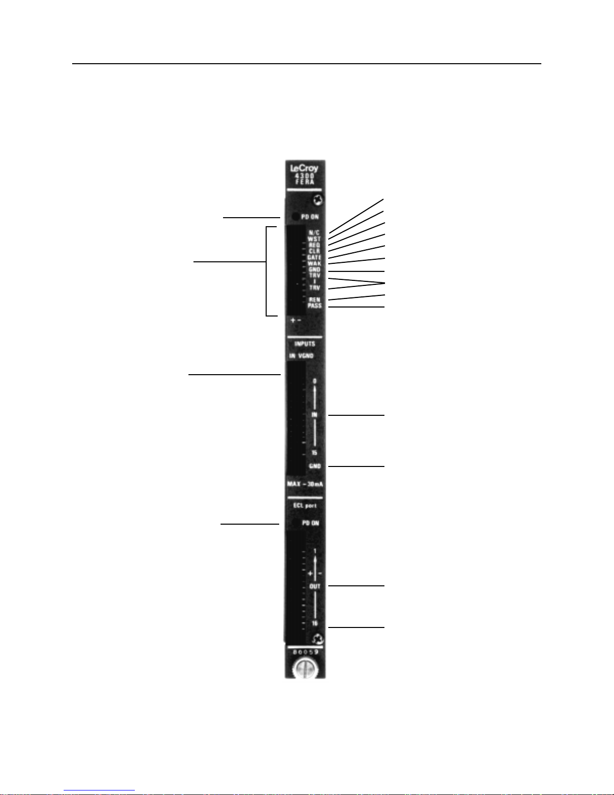
Pull Down ON (LED
indicator) indicates
that pull down and
input resistors are
mounted on Command
bus (Sec. 1.15)
Command Bus
Analog Inputs
(Sec 1.3)
MODEL 4300B
FRONT-PANEL
Not connected
Write Strobe (Sec. 1.11)
Readout Request (Sec. 1.11)
Clear (Sec. 1.4)
Gate (Sec. 1.5)
Write Acknowledge (Sec. 1.11)
Ground
Test Reference Voltage (Sec. 1.7)
Readout Enable (Sec. 1.11)
Readout Enable PASS (Sec. 1.11)
Pull Down on (LED
Indicator) indicates
that pull down
resistors are mounted
on the ECL output
Port (Sec. 1.15)
Common Virtual Ground
(Sec. 1.3)
Ground (Sec 1.3)
ECL output port
(Sec 1.10)
Last 2 pins not
connected
11
Page 10

PRODUCT DESCRIPTION
1.1 General The LeCroy Model 4300B FERA contains 16 independent charge-todigital converters with common GATE and common CLEAR.
Four basic factory options are available:
a. 8 or 9 bits with 100 ohm impedance
b. 8 or 9 bits with 50 ohm input impedance
c. 10 or 11 bits with 100 ohm input impedance
d. 10 or 11 bits with 50 ohm input impedance.
The options a, b and c are only produced for large quantities. The
resolution on each of the above versions may be adjusted via jumpers
and an internal potentiometer (see Section 2.13 for details).
1.2 Specifications
LeCroy Input Resolution Conversion Range Sensitivity Digital Values
4300B Impedance Time Typical Typical Full Over
MOD Scale Flow
ohms bits µsec pC pC/count counts counts
100 100 8 1.8 128 0.5 255 2047
500 50
110 100 9 2.8 256 0.5 511 2047
510 50
200 100 10 4.8 256 0.25 1023 2047
600 50
210 100 11 8.5 480 0.25 1919 2047
610 50
An 8-bit register (Status Register) and a memory (Pedestal Memory),
containing the individual pedestal (or offset) values to be subtracted from
each ADC, allow different readout modes of the 16 digitized ADC values.
Both the Status Register and Pedestal Memory must be previously
loaded via CAMAC. Data may be read out either via the CAMAC
dataway or the ECL port. The state of the Status Register determines the
readout modes. The ECL port output, located on the front-panel, is first
activated and delivers ADC data sequentially in words of 16 bits (8 to 11
bits of data plus 4 subaddress) at differential ECL levels. When data are
ready to be read at the ECL port, the REQ output is activated.
In CAMAC mode, data are also read out in 16-bit words in either random
access or sequential CAMAC readout (Q stop mode). The CAMAC
readout can only be carried out after completion of ECL port readout.
When data are ready for readout via CAMAC dataway, a LAM may be
generated and there is a Q response to the readout function F(2). The
data read out mode via these two ports may be independently selected
and programmed to be in one of three states: 1) raw; 2) with the pedestal subtracted; or 3) compacted, i.e., all data < 1 are eliminated (Zero
suppression).
A system for testing the 16 ADCs is incorporated in the Model 4300B.
The test is initiated by the CAMAC command F(25) A(0). This command
opens the ADC GATEs and applies, at the input of each one, a charge
proportional to the continuous voltage that must be given on the front
panel TRV input.
13
Page 11

The Model 4300B will be in one of two states: “ready” or “busy”; depending on the GATE and CLEAR signals sent via either the front-panel or
CAMAC command. After a CLEAR, the module is in the “ready” state,
i.e., ready to receive a GATE (front-panel or test): the logic and the ADCs
are permanently cleared. It is only in the “ready” state that the Status
Register and the Pedestal Memory may be loaded or read via CAMAC.
After a GATE (front panel or test): the module changes to the “busy”
state and no other GATE signal will be accepted. The GATE disables the
reset, opens the ADCs and initiates the charge digitization logic. At the
end of the conversation time, data readout is enabled. At this time,
depending on the state of the Status Register and the ADC data values
to be read, one of four conditions may be present:
a. Data readout via ECL port and CAMAC. In this case, the ECL port
must be read first and only upon its completion can CAMAC readout
take place.
b. Data readout via ECL port only. In this case, only the ECL port is
enabled.
c. Data readout via CAMAC only. Here, the ECL port readout is not
enabled; CAMAC readout is enabled immediately at the end of
conversation.
d. No data to be read. In this case, no data readout is enabled.
To eliminate unwanted data or accept further GATE after data read out, a
CLEAR must be applied to the 4300B unit (see Figure 1.1).
1.3 Analog Inputs The 16 analog inputs are designed for negative signals with respect to a
floating common signal ground (Common Virtual Ground) which is
coupled to the module ground via capacitors. Input impedance is 50 or
100 ohm with respect to the Common Virtual Ground. All 16 inputs are
protected against positive signals by diodes connected to the module
ground, and against too high amplitude negative signals by diodes
connected to a -3 V potential. The Common Virtual Ground is also
protected against large swings of voltage by two diodes connected to the
module ground.
If the user wishes to connect the Common Virtual Ground to the module
ground, the 16 upper right hands pin (VGND, Common Virtual Ground)
may be connected to the lower 2 pins (GND, module ground), of the
input connector. Another option is to solder a jumper between the two
points designed for this function located on the printed circuit board (see
Figure 1.5).
1.4 Clear Function A clear is initiated by a front-panel CLEAR input and by CAMAC functions Z, C or F(9) A(0) strobed by S2. Front-panel CLEAR and F(9) A(0)
have priority over the GATE signal and care must be taken not to generate any gate in coincidence with them. As a result, the GATE signal
duration would be modified.
14
These commands set a latch maintaining the clear level (“ready” state of
module) until the next GATE signal. The front ends of the ADCs require
at least 2 µs after a clear to guarantee a ± 1 count precision. They are
Page 12

automatically cleared at the end of conversation after digitized charges
have been memorized. Thus, a 2 µs delay before a new GATE is only
necessary when the CLEAR command is used during conversation. After
power-on, a clear function must be applied for the module to be in the
“ready” state.
1.5 External Gate
Input (GATE) A GATE command is effective only if the module is in the “ready” state
and if the CLEAR command is released. The GATE input is inhibited
when the I (CAMAC Inhibit) line is ON. A 100 ns integrator is placed on
the I line.
A valid GATE signal commands the following functions:
a. Releases the clear on the ADC front ends.
b. Opens ADC gate for its entire duration.
c. Enables ADC pedestal injection circuit.
d. The end of the GATE starts conversation, switches the module to the
“busy” state and inhibits the GATE input.
The GATE signal must precede analog input signals by a minimum of
20 ns and its length may vary from 50 ns to 500 ns. Use of a GATE
longer than 500 ns is possible, but it may require adjustment of ADC
pedestals (see Sections 1.6 and 2.3).
1.6 ADC Pedestals The 16 ADC pedestals are generated by the injection of a small charge
at the leading edge of the GATE. The pedestal value may be adjusted via
an internal potentiometer, 0 adjustment. A common circuit compensates,
to a large degree, the variations of the pedestals with respect to GATE
width.
The Model 4300B is adjusted so that the pedestals remain between 1
and 13 pC for GATE durations of 50 ns to 500 ns. For a GATE larger
than 500 ns, some ADCs channels may have pedestals below 0 pC. The
charge injected by the O adjustment potentiometer must be increased to
obtain at least 1 pC.
The pedestals may be subtracted from the ADC value during ECL port or
CAMAC readout, independently.
1.7 Test Function The test function is initiated by the CAMAC command F(25) A(0) strobed
by S2, when accepted, Q response is given. This function is accepted
only when the module is in the “ready” state; no Q response will be given
if the command is not accepted.
The test function controls the following operations:
a. Releases the clear on the front end of the ADCs.
b. Opens the GATE for a duration of 550 ns, during which time no
signal is allowed on any of the analog inputs, although the cable may
remain connected. The gate input may, but need not, be blocked by
the CAMAC command I.
15
Page 13

c. Enables the ADC pedestal injection circuit.
d. Applies a charge to the 16 ADCs that is proportional to the DC
voltage present on the front-panel TRV input.
e. At the end of the GATE starts conversation and switches the module
to the “busy” state.
The Test Reference Voltage (TRV) input is referenced to module ground.
The voltage applied on TRV may vary between 0 and +10.24 V which
corresponds to a charge of 0 to 512 pC per ADC. The test charge is not
affected by the common mode of the Common Virtual Ground with
respect to the module ground.
1.8 Pedestal Memory The Model 4300B contains an 8-bit, 16-word Pedestal where each word
corresponds to an ADC pedestal (or offset) value to be subtracted during
readout (maximum digital value 255). This memory may be loaded or
read via CAMAC in random access mode if the module is in the “ready”
state. The memory must be reloaded after a power-on, but is not affected
by clear functions.
Pedestal values are written in the memory with the CAMAC function
F(17), strobed by S1, and subaddresses from A(0) to A(15) corresponding to channels 0 to 15. The 8 bits are written on lines W1 to W8. Readout of pedestal memory values is performed with F(1) and the same
subaddresses, A(0) to A(15). The 8 bits to be read out are sent on lines
R1 to R8. F(17) A(0) to A(15) and F(1) A(0) to A(15) are possible only
when the module is in the “ready” state; there is no Q response if they
cannot be accepted.
1.9 Status Register The Status Register is composed of two distinct sections. See Table
1.1.a. The low order 8-bit Virtual Station Number (VSN) determines the
address of the data source during readout, while the 8 other bits determine the readout modes.
The 15 bits of the Status Register are loaded by the CAMAC function
F(16) A(0) strobed by S1 with data written on lines W1 to W15. The value
of the Status Register may be read with the function F(0) A(0) on lines
R1 to R15. These two functions are possible only when the module is in
the “ready” state; there is no Q response if they cannot be accepted.
After a power-on, the state of the module is undetermined. The CAMAC
initialization function Z will enable the 7 command bits, but will not affect
the VSN register. The other clear functions have no effect on the Status
Register.
The functions of the 8 Status Register command bits are:
EPS: ECL port Pedestal Subtraction (W9,R9).
EPS = 1: subtracts, from each ADC channel, the value of
its pedestal (offset) contained within the Pedestal Memory
during the ECL port readout.
EPS = 0: no pedestal subtraction during ECL port readout.
16
Page 14

ECE: ECL port data Compression Enable (W10, R10).
ECE = 0: Blocks the suppression of data < 1 for ECL port
readout. All 16 ADC values, with or without pedestal
subtraction, are sent sequentially to the ECL port.
Note: The channel subaddress is not provided and the data
cannot be negative (minimum value 0).
ECE = 1: Activates, after conversion, a data compression
cycle for ECL port readout; all data < 1 are eliminated. This
procedure takes 2.5 µsec. If there are no valid data, ECL
port readout will not take place and CAMAC readout will
automatically be enabled. In order to determine the origin of
data, a Header Word is identified by the 16th bit which
always = 1, and is composed of 8 VSN (Virtual Station
Number) Status Register bits and 4 WC (Word Count) bits
indicating the number of ADC channels to be read
(1 = 1 channel, ..., 15 = 15 channels, 0 = 16 channels).
EEN: ECL port ENable (W11, R11).
EEN = 1: Activates, after conversation, a data compression
cycle for ECL port readout; all data < 1 are eliminated. This
procedure takes 2.5 µsec. If there are no valid data, ECL
port readout will not take place and CAMAC readout will
automatically be enabled. In order to determine the origin of
data, a Header Word is sent as the first word and the
channel subaddress is included in the ADC data word. The
Header Word is identified by the 16th bit which always = 1,
and is composed of 8 VSN (Virtual Station Number) Status
Register bits and 4 WC (Word Count) bits indicating the
number of ADC Channels to be read (1=1 channel,
15=15 channels, 0=16 channels).
EEN = 0: The ECL port readout is disabled, and CAMAC
readout is immediately enabled after a conversation. The
commands EPS and ECE are ignored.
EEN = 1: Enables ECL port readout procedure. CAMAC
readout is enabled at the end of ECL port readout.
CPS: CAMAC Pedestal Subtraction (W12, R12).
CPS = 1: During CAMAC readout activates the subtraction
of pedestal (or offset) value of each ADC contained within
the Pedestal Memory.
CPS = 0: No subtraction takes place.
CCE: CAMAC data Compression Enable (W13,R13).
CCE = 0: Disables data compression in CAMAC readout. All
16 ADC values, with or without pedestal subtraction, can be
read by CAMAC. The channel subaddress is not provided
and data cannot be negative (minimum value is 0).
17
Page 15

CCE = 1: Enables the data compression cycle after an
ECL readout or conversation, for sequential CAMAC readout
mode only. This procedure takes 2.5 µs and all data < 1
count are eliminated. If no data are valid, the CAMAC
sequential readout will not be initiated. The Header Word
and the data are structured in the same way as for ECL port
readout.
CSR: CAMAC Sequential Readout (W14, R14).
CSR = 0: Enables CAMAC random access readout. Data
compression is blocked (CCE indifferent). The 16 ADC data,
with or without pedestal subtraction, may be read without
their subaddresses with the function F(2). Subaddress A
determines the channel to be read (A(0) = channel 0, etc.).
The Q response to this function is given when CAMAC
readout is initialized and as long as no clear function has
been applied.
CSR = 1: Enables the procedure for sequential CAMAC
readout. Valid data may be read sequentially with the
function F(2) A.(0) to A(15); (subaddress A is not decoded).
At the end of S2, the following data word is accessed. A Q
response is given for each valid data word until the last data
word (Q stop mode). If after compression no valid data are to
be read, the Q response is inhibited.
CLE: CAMAC Look-at-me Enable (W15,R15).
CLE = 0: LAM output is inhibited.
CLE = 1: Results in the setting of LAM as soon as data are
ready to be read by CAMAC. In the case of compressed
sequential readout where there are no valid data, the LAM
will not be set.
OAFS: Overflow Suppress (W16, R16).
This bit sits as the ECE or the CCE bits but operating both on the zeros
and the overflows. That is when OFS = 1 not only zeros (< 1) but also
overflows will be suppressed. In particular, when ECE = 1 the suppression will be performed on the CAMAC readout. This procedure takes
again 2.5 µs as in the case of zero suppression alone.
Note: The CAMAC initialization command Z sets the Model 4300B
Status Register for the ECL port readout to be followed by CAMAC
sequential readout with transmission of the LAM. Both readouts will have
pedestal subtraction and data compression. (See Readout Timing
Diagram Figure 1.1).
1.10 ECL Port Output The ECL port output delivers 16-bit data words at complementary ECL
levels. The maximum output frequency is 10 MHz. If the user wishes to
connect this output to a bus on which other outputs are already connected, the pull-down resistors must be removed from the module (see
Figure 1.5). When lit, the LED indicator (PD. ON), located over the ECL
port connector, indicates that these resistors are mounted. When several
18
Page 16

modules are connected on the ECL port bus, only the positive ECL
outputs are used, the negative ECL outputs may be connected to ground
to improve shielding. See Table 1.1.b for data format.
1.11 ECL Port Readout
Handshake In order to provide for the synchronization of the ECLbus, the following
signals are utilized. These signals, transmitted via front-panel command
connectors, are described below:
a. REQ (REQuest output) is activated as soon as data to be read by
the ECL port are ready and remains until the last data has been read
(or a clear function has been given).
b. REN (Readout ENable input) enables the ECL port output if REQ
signal is present, or the PASS output if the REQ signal is released.
The REN signal must be maintained throughout the entire ECL port
readout. The REN input is automatically considered as active if it is
not connected.
c. PASS (PASS output) is enabled by the REN input if the REQ signal
is not present. This signal indicates that the ECL port readout is
complete, or that there is nothing to be read in the module.
d. WST (Write STrobe output) indicates that a data word is present on
the ECL port output. WST is given a minimum of 10 ns after the data
and its minimum duration is 40 ns.
e. WAK (Write acknowledge input) indicates that the data on the ECL
port has been accepted. The module with control of the ECLbus
releases WST and passes on to next data word. WAK can be
released after WST is cleared and its duration must be a minimum of
30 ns.
The ECL port control signal sequence is as follows (see ECL port Timing
Diagram, Figure 1.2): When data are ready, the REQ is generated and
inhibits the PASS output. Once REN is received, the first data word is
sent to the ECL port output and the WST is activated. This state remains
unchanged until a WAK signal is applied; this allows the readout to be
delayed if necessary. As soon as the WAK is received, the WST is
released, but an internal protection keeps the WST duration from being
less than 40 ns. The trailing edge of the WST loads the next data word
on the ECL port. In order to permit the delay of the readout, WS is
reactivated after approximately 50 ns.
When the WAK is received after the last data word has been read, the
REQ signal is disabled and the REN signal is routed to the PASS output,
indicating that the readout is complete and enabling the readout of the
next 4300B module.
The Model 4300B is designed to allow direct connection of WST on WAK
and thus obtain data on the ECL port at a frequency of approximately
10 MHz.
After a Z command, the ECL port readout is automatically enabled along
with pedestal subtraction and data compression.
19
Page 17

1.12 Halt of Readout
on the ECL Port It is possible to momentarily interrupt an ECL port readout in progress in
three different ways.
a. If a data transfer is authorized by the REN input, this signal should
be released during a time = (WAK response + 20 ns) in order to
avoid loss of data. The ECL port outputs and WST are inhibited
when REN is released.
When several 4300B modules are connected on the same ECL port
bus, one must take into account the fact that the REN signal, applied
to the first module, must transit through all the others (PASS output
connected to REN input of the subsequent module). The transit time
between the REN input and the PASS output for an empty module is
3 ns, typical.
b. By not initiating the WAK in response to a WST. In this case, the data
on the ECL port and the WST remain on as long as a WAK signal is
not received.
c. By not releasing the WAK signal after a WST. In this case, the WST
is released and the next data are placed on the ECL port output, but
it is only upon release of the WAK that the WST will be turned on
again.
1.13 CAMAC Readout CAMAC readout of the ADC data by function F(2) A(0 to 15) may be
performed in either random access mode or sequential mode. Selection
of the readout mode is determined by the CSR bit of the Status Register.
CSR = 0 enables random access readout. The channel addressed for
readout is selected by the subaddress A. The Q response to the readout
function is delivered once the data are available as long as a clear
function has not yet been applied. Data compression is suppressed and
all 16 data words may be read. Pedestal subtraction commanded by
CPS may be carried out or not. The data are transferred on lines R1 to
R11 without the channel subaddress (R12 to R16 = 0). CSR =1 enables
sequential readout. Subaddress A has no effect. Passing from one data
word to another is carried out at the end of the readout of the last data
word.
When CCE = 0; data compression is suppressed and the 16 data words
may still be read. Pedestal subtraction commanded by CPS may be
carried out or not. The data are transferred on lines R1 to R11 without
the channel subaddress (R12 through R16 = 0).
When CCE = 1; data compression is enabled and the data <1 are
eliminated from readout. Usually, pedestal substraction will be enabled
(CPS = 1) due to the fact that the ADC pedestals are greater than zero.
If no valid data are available, readout will not take place (no Q response).
The first word to be read is the Header Word composed of the 8 bits of
VSN (Status Register on R1 to R8), the 4 bits of WC (indicating the
number of data words to be read on R12 to R15), and of the identification
bit (R16 = 1). The valid data (from 1 to 16) are then given sequentially
(on R1 to R11) accompanied by the channel subaddress (on R12 to R15,
R16 = 0). See Table 1.1b for data format.
20
Page 18

When OFS = 1 and CCE = 1 both the data < 1 and the overflows are
eliminated from readout. Pedestal subtraction should be disabled if the
user wants to eliminate just overflows. Z function automatically initializes
CAMAC sequential readout mode with pedestal subtraction and data
compression.
1.14 LAM Handling The LAM is inhibited if the CLE bit of the Status Register is off. If CLE is
ON, LAM is activated as soon as the data are ready for CAMAC readout.
During sequential readout, the LAM is cleared after readout of the last
word.
The states of the LAM may be tested by the following functions:
F(8) A(0) gives Q = 1 response if LAM present
F(10) A(0) gives Q = 1 response if LAM present and clears LAM at
S2 if LAM was present.
The LAM is also cleared by the following functions: front-panel CLEAR
input and Z, C, F(9) A(0), strobed by S2. After an initialization Z function,
the CLE command is set to ON.
1.15 FERA System
Connections The Model 4300B may function independently or as part of larger system
(of up to 22 4300B modules) controlled by the Model 4301, FERA Driver
(see Figure 1.3 and Model 4301 User’s Manual). This driver sends or
receives all the signals necessary to operate the system. The following
interconnections must be made to ensure proper operation of the
system:
a. Command Bus; between Model 4301 and each Model 4300B
(8 x 2 wire flat cable).
b. ECL port data Bus: between INput connector of Model 4301 and
each Model 4300B (17 x 2 wire flat cable).
c. Readout Enable/Pass: between REQ output of Model 4301 and REN
input of the first Model 4300B to be read. Also, between each Model
4300B, the PASS output is to be connected to the REN input of the
next unit; 1 x 2 wire cable (LeCroy type STP-DC/02-00).
When more than two 4300B modules are connected to these busses, the
input matching and pull-down resistors must be removed from ECL port
and Command busses on all 4300Bs except the one located opposite
the Model 4301 FERA Driver as it serves as a terminator for these
busses (see Figures 1.3 and 1.5). To check the set up, it is sufficient to
observe the PD ON LED indicators on the Command and ECL port bus.
On these two busses, all LEDs on modules placed between the terminator module and the driver should be off.
21
Page 19

The Model 4301 FERA Driver is designed to receive and distribute all
signals necessary for system functioning. It serves as an intermediary
between the external logic and the 4300B modules for the following
signals and commands:
a. Via Command bus
- Distributes the CLEAR received on the front-panel or by a CAMAC
command.
- Distributes the GATE received on the front-panel.
- Delivers the CAMAC programmable TRV for the test.
- Receives the REQ signals from the 4300B modules and, after an
adjustable delay covering the dispersion of these REQ signals,
generates RQO and REO signals. RQO represents the logic OR of
all REQ signals on the bus. REO is in addition gated by IRI.
- Regenerates on the front-panel the WST signal received from the
4300B modules.
- Distributes to the 4300B modules the response signal WAK
received from the front-panel.
b. Via the ECL port bus
- Receives and translates single-ended ECL level data from the
4300B modules and converts them to ECL complementary levels
for the front-panel data output connector.
c. Via Enable/pass readout bus.
- Generates the ECL port readout signal, REN, received from the
front-panel.
See Figure 1.4, Model 4301 FERA Driver Block Diagram.
1.16 Packaging and
Power Requirements The Model 4300B FERA is packaged in a standard # 1 CAMAC module.
It dissipates a total of 30 watts with the following current distribution:
< 0.1 A at +24 V
< 2.1 A at +6 V
< 2.7 A at -6 V
The current at +24 V depends on the current of the 16 analog inputs. It is
equal to 65 mA plus the mean of the sum of all input currents.
Note: When all output pull-down and input matching resistors are
removed, the current at -6 V is reduced to 2.4 A.
4300B Status
T1: Depends on the resolution. 8 bits = 1.8 use; 9 bits = 2.9 µsec;
10 bits = 4.8 µsec; 11 bits = 8.5 µsec.
T2: Depends on the ECE status.
ECE = 0 : T2 = 0
ECE = 1 : T2 = 2.3 µsec
22
Page 20

T3: Depends on the ECE status, data values and ECL port readout rate
(> 100 nsec per word).
ECE = 0 : T3 = 16 (> 100 nsec per word);
ECE = 1 and all or part of the data = 0 : T3 = 2 to 17
(> 100 nsec per word);
ECE = 1 and all data = 0 : T3 = 0 and the ECL port readout is
suppressed.
T4: Depends on the CSR and CCE status.
CSR = 0 or (CSR = 1 and CCE = 0) : T4 = 0
(CSR = 1 and CCE = 1) : T4 = 2.3 µsec.
T5: Depends on the CCE status, data values and CAMAC
readout rate (> 1 µsec per word).
CCE = 0 : T5 = 16 (> 1 µsec per word).
CCE = 1 and all or part of the data = 0 : T3 = 2 to 17
(1 µsec per word).
CCE = 1 and all data = 0 : the CAMAC sequential readout and LAM
are suppressed.
Note: This diagram does not define the logic states, low = OFF and high = ON.
Figure 1.1: READOUT TIMING DIAGRAM
23
Page 21

Figure 1.2: ECL PORT TIMING DIAGRAM
All times in nsec, typical.
Note: This diagram does not define the logic state of the signals: low = OFF and high = ON.
24
Page 22

Figure 1.3: FERA SYSTEM CONNECTIONS
25
Page 23

Figure 1.4: MODEL 4301 FERA DRIVER BLOCK DIAGRAM
26
Page 24

Figure 1.5: LOCALIZATION OF REMOVABLE RESISTORS AND VGND-GND JUMPER
27
Page 25

W16/R16 W15/R15 W14/R14 W13/R13 W12/R12 W11/R11 W10/R10 W9/R9 W8/R8 W1/R/1
OFS CLE CSR CCE CPS EEN ECE EPS VSN
Loaded by F(16) A(0) Read by F(0) A(0)
Table 1.1.a: STATUS REGISTER FORMAT
28
Page 26

Without Zero or Zero-and-Overflow Suppression:
ECL port readout: EEN=1, ECE=0, OFS=X
CAMAC readout: CSR=1, CCE=0, OFS=0
R16 R11
CHANNEL 0
CHANNEL 15
0
0
0
0
0
0
DATA: 8-bit resolution; 0 to 255; overflow=2047
9-bit resolution; 0 to 511; overflow=2047
10-bit resolution; 0 to 1023; overflow=2047
11-bit resolution; 0 to 1919; overflow=2047
With Zero or Zero-and-Overflow Suppression
ECL port readout: EEN=1, ECE=1, OFS=0 or 1
CAMAC readout: CSR=1, CCE=1, OFS=0 or 1
DATA
DATA
DATA
DATA
DATA
DATA
R1
Always
16 words
HEADER WORD
FIRST CHANNEL
CHANNELS WITH
DATA > 0
LAST CHANNEL
R16 R11
WC = 0 to 15
1
0
0
0
0
0
FIRST SA
SA
SA
SA
LAST SA
0
00
R8
VSN
DATA
DATA
DATA
DATA
DATA
VSN: Virtual Station Number Loaded in the Status Register.
WC: Number of data words following the header word, 0 indicates 16 data words.
DATA: 8-bit resolution; 0 to 255; overflow=2047
9-bit resolution; 0 to 511; overflow=2047
10-bit resolution; 0 to 1023; overflow=2047
11-bit resolution; 0 to 1919; overflow=2047
SA: Channel Subaddress
R1
2 to 17
words
Table 1.1b: READOUT FORMAT
29
Page 27

OPERATING INSTRUCTIONS
2.1 GENERAL The circuitry of the LeCroy Model 4300B FERA can be divided into the
following eleven basic parts:
a. CLEAR and GATE functions
b. Charge to time converters (16 channels)
c. Test circuit
d. Digital interpolators (16 channels)
e. Real time counters (16 channels)
f. Clock generator
g. Pedestal memory
h. Data compression and readout logic
i. ECL port readout circuit
j. CAMAC readout circuit
k. CAMAC functions decoder
For a general overview, see the 4300B Block Diagram (Figure 2.1). This
block diagram gives only the principles of functioning - for further details,
consult the 4300B schematics located in the back pocket of this user’s
manual.
The Model 4300B adjustments which will be discussed in the following
paragraphs are located on the inner left-hand side of the module (cover
must be removed to access).
Warning: Only the pedestal value adjustment (see Section 2.3) and the
ADC resolution adjustment (see Section 2.13) can be made without
modifying the modules performance. Other adjustments must not be
modified without adequate control.
2.2 CLEAR and
GATE Functions The state of the BUSY flip-flop determines the two module states “ready”
and “busy”. It is cleared (“ready state) and remains at zero throughout
the duration of a CLEAR function. This CLEAR function is generated by
the front-panel CLEAR input or the CAMAC decoder (Z.S2, C.S2, F(9)
A(0).S2). This function also clears and maintains the CLEAR flip-flop of
the charge-to-time converters. In the “ready” state, the clock generator
and readout logic circuits are inhibited and the GATE input (or TEST) is
enabled. The GATE signal, generated by the front-panel GATE input or a
monostable triggered by the test function F(25) A(0).S2, initiates the
following command sequence:
a. Sets the CLEAR flip-flop, suppressing clear of the charge-to-time
converters.
b. Opens the charge-to-time converter gates.
c. Enables the pedestal injection circuit.
d. At the end of GATE, sets the BUSY flip-flop (“busy” state of module).
Setting the BUSY flip-flop results in the following functions:
a. Inhibits the front-panel Gate input and on the CAMAC decoder;
inhibits all functions except data readout and clear.
b. Triggers the two digitization control monostables.
31
Page 28

The adjustable FS (Full Scale) monostable enables the clock generator
(Gray code) and the real time scale memorization latches. The end of
this monostable signal clears the CLEAR flip-flop of the charge-to-time
converters and triggers the readout circuit.
The duration of the FS monostable is adjusted (via the FS potentiometer)
to produce a number of clocks slightly larger than the number of clocks
necessary for the digitization of the Full Scale. Its length depends on the
ADC resolutions (see Section 2.13). The CAMAC command I, integrated
by 100 nsec, inhibits the GATE input.
2.3 Charge-to-Time
Converters The charge-to-time conversion is provided for each channel by a mono-
lithic integrated circuit, LeCroy Model MQT200F. This circuit is based on
the dual ramp Wilkinson principle and the integration of the charge by a
capacitor. This capacitor is charged during the entire duration of the
GATE by the input current and discharged by a constant current after the
closing of the GATE. The time conversion is determined by the duration
of the discharge which is proportional to the amplitude of the charge
injected on the capacitor.
The following description refers to Figure 2.2. The MQT200F analog
input impedance is approximately 0 ohm and its potential is equal to that
of the common ground VGND. A terminating resistor of 50 ohm (or
100 ohm), mounted in series with this input, converts the input voltage to
an input current (iin). In the quiescent state, a switch shunts the inputs of
the output comparator. Time output is thus at the zero logic state.
When a GATE is applied, the input current iin is switched on to the
integrating capacitor, the output comparator MOSFET is switched off and
the pedestal injection circuit is activated. The charge current of the CI
integration capacitor is thus equal to:
IC = iIN + iP - IRU + I
PC
iIN is the input current.
iP is the current generated by the discharge of Cp, the capacitor of
the pedestal injection circuit.
IRU is the constant discharge of the integration capacitor.
IPC is the constant current permitting compensation of IRU and all
leakage currents to reduce the pedestal dependence on the GATE
width.
Time output is turned ON.
On the trailing edge of GATE, the input charge currents iIN are switched
back to the +15 V power supply and only the constant current I
RU
discharges the integration capacitor. The MOSFET shunts on the inputs of
the output comparator is switched on again at the end of the conversion
(FS monostable). The time output is turned OFF when the integration
capacitor voltage level reaches the output comparator reference voltage
value; its duration is proportional to the gated input charge.
32
Page 29

The IRU currents, which determine the ADC gains, are controlled by the
VRU supply, adjustable via the VRU potentiometer. The VRU potential is
adjusted to obtain an average of 0.5 pC/count for 8 and 9 bits of resolution to 0.25 pC/count for 10 and 11 bits of resolution. The pedestal
compensation IPC currents are controlled by a voltage adjustable by
means of the P potentiometer. This voltage is adjusted so that the
average pedestal variation is zero with a GATE varying between 50 nsec
and 500 nsec. This adjustment depends on the VRU voltage. The
amplitude of the pedestal injection charges is adjustable by means of the
O potentiometer. It is adjusted to obtain an average pedestal of 8 pC.
This adjustment does not affect any other adjustment and if necessary
may be readjusted for GATE width greater than 500 nsec.
2.4 Test Circuit The test charge is injected at the input of the MQTs by the discharge of a
200 pf Ct capacitor, via a resistor fan-out (see Figure 2.2). An amplifier,
controlled by the voltage applied on the TRV input, charges Ct to a
voltage equal to that of the TRV while compensating the voltage difference between the VGND and the module ground. The test charge may
be adjusted via the T potentiometer. It is adjusted to obtain an average
charge on each ADC of 50 pC/V.
The test is controlled by a monostable triggered by the CAMAC function
F(25) A(0).S2. The monostable output width is 550 nsec. It opens the
GATE, and after a delay of 20 nsec, turns on the MOSFET switch, which
discharges the Ct capacitor into all 16 analog inputs through the 16
resistor fan out.
2.5 Digital Interpolators In order to accelerate the time to digital conversion, digital interpolators
are used between the time output of the MQT200Fs and the real time
counters. The following description refers to Figure 2.3. Each interpolator
is made of four latches controlled by four clock signals at 4 nsec intervals. Looking at the different consecutive states of these four clock
signals, it can be seen that the time function of the four signals follows a
gray code rule, i.e., only one of the four signals changes its state at a
time.
Each digital interpolator memorizes the state of the gray code when it
receives a high to low transition from the time output. During readout, the
four gray code bits are converted into binary code to form the three least
significant bits of the data word. The real time counter clock is generated
by the fourth interpolator latch output. The high to low transition of this
output indicates the transition from state 7 to 0, and results in the
incrementation of the real time counter.
2.6 Real Time Counters The 16 real time counters are packaged in four hybrid, LeCroy type
ls408, circuits. Each circuit contains four independent, 8 bit scalers, each
with latches and tri-state out buffers. The following description refers to
Figure 2.3. At the end of a GATE signal, the real time counters are
cleared by the 400 nsec monostable and the latches are activated for the
entire digitization duration by the FS monostable. After the digitization,
these latches memorize the state of the real time counters. During the
interpolator readout a transition may appear on the clock of the real time
counters. The real time counters are incremented by each high to low
interpolator output transition, that is, in module 8. The three bits of the
interpolator associated with the eight bits of the real time counter form
the eleven bits of the ADC data word.
33
Page 30

2.7 Clock Generator The reference clocks are generated by a voltage controlled oscillator
controlled by an LC tank. Its oscillation frequency is adjusted to 125 MHz
by means of the variable F capacitor. This frequency is divided by the
gray code generator for the interpolator command.
The following description refers to Figure 2.3. To synchronize its phase,
the 125 MHz oscillator is stopped for 400 nsec by a monostable triggered
at the end of the GATE signal. Simultaneously, the gray code clear is
released and remains so until the FS monostable resets.
The gray code generator consists of a group of four flip-flops dividing the
125 MHz oscillator frequency into four clocks of 31.25 MHz. These four
clocks are separated from each other by 4 nsec to form the gray code
and are distributed, via drivers, on two 4-line busses for the odd and
even channel interpolators. The resistor terminations of these busses are
polarized by a power supply (-2 V). It is adjustable by means of the
-2 V potentiometer. This power supply influences the differential linearity
and the clock output levels of the interpolators. It is adjusted between
-1.8 V and -2 V for accurate operation.
2.8 Pedestal Memory The pedestal memory consists of two 16 x 4 bit memories. When the
Model 4300B is in “ready” state, their select inputs are enabled. They
may be loaded by the CAMAC function F(17).S1) or read by F(1)S2. The
subaddress A(0 to 15) are applied to the internal address bus via a
multiplexer. During readout, the drivers on lines R9 to R16 are disabled.
When the module is in the “busy” state, the memory outputs are enabled
only if the pedestal subtraction is programmed. In the case where the
memory outputs are disabled, zero subtraction is guaranteed by the pullup resistors.
2.9 Data Compression
and Readout Logic During readout, the readout logic addresses one of the ADC channels
and its corresponding pedestal in the Pedestal Memory. The 11 bits of
this ADC data and its pedestal are applied to the subtractor inputs. The
11 bits resulting from the subtraction are loaded into the Data Memory
register. The output of the zero detection, (performed by a diode AND
function is reintroduced into subtractor to disable the Carry output for
values equal to or smaller than zero. It also sets the flip-flop clear of the
Data Memory.
The overflow command, selected on bits 27 to 210 by means of jumpers A,
B, C and D to match the ADC resolutions, sets the flip-flop which disables the Data Memory outputs and the overflow state (2047) is assured
by pull-up resistors. The position of the jumpers are as follows:
8 bit resolution B only (256)
9 bit resolution C only (516)
10 bit resolution D only (1024)
11 bit resolution A,B,C,D (1920)
34
Page 31

The command bits of the Status Register determine the operation mode
of the readout logic. If the module is in the “ready” state, the Status
register may be loaded with the function F(16) A(0).S1 or read with F.(0)
A(0). The function Z.S2 clears the Status Register, setting the command
bits in their true state. Two flip-flops control the readout sequence:
The first flip-flop, enabled by the end of a conversion (reset of FS
monostable), activates the ECL port readout procedure if the bit EEN is
ON.
The second flip-flop is enabled by the end of an ECL port readout, or by
the end of a conversion if the bit EEN is OFF. It activates the CAMAC
readout procedure and commands the selection of bits EPS and ECE or
CPS and CCE for the operation mode of the readout logic. These two
flip-flops are cleared by the end of CAMAC readout or by a CLEAR
command.
A start-stop oscillator (RF), adjusted to 7 MHz by means of the variable
RF adjustment, provides the clocks for the readout logic. This readout
logic operates in two different modes for either ECL port or CAMAC
readout.
a. Data compression is disabled (ECL port: EEN = ON with ECE = OFF,
CAMAC: CSR = ON with CCE = OFF, the special case where CSR =
OFF is considered as identical to data compression disabled.
Channel addresses are generated by the Address Scaler and
demultiplexer. The RF oscillator delivers two clock pulses. The first
pulse initializes the Address Scaler at address zero. The second
pulse loads the data from channel zero in the Data Memory,
increments the Address Scaler and starts the external readout via
the RE flip-flop.
b. Data compression enabled (ECL port: EEN + ON with ECE = ON,
CAMAC: CSR = ON with CCE = ON ).
A 16 channel readout cycle, addressed by the Address Scaler, is
executed. The Word Count Scaler counts the number of valid data
and addresses the Address Memory. The addresses of the valid
channels are loaded in this memory.
The RF oscillator delivers 18 clock pules. The first pulse initializes the
Address Scaler and the Word Count Scaler. The 16 following pulses
increment the Address Scaler and load the Address Memory with the
address of valid channels. The Word Count Scaler is incremented and
the RE flip-flop set only if the Carry output of the subtractor is enabled.
The last pulse decrements the Word Count Scaler, commutes the
channel addressing to the Address Memory output, and enables the
external readout with the Header Word as the first data word (or the end
of readout if no valid data present).
The RE, external Readout Enable, command is delivered either on the
ECL port readout circuit by the command ER, or on the CAMAC function
decoder and the LAM circuit by the command CR.
35
Page 32

Note: The valid channel address is also loaded in the Data Memory, but
these 4 bits are maintained at zero for ECL port and CAMAC readout
without compression or CAMAC random access. If the user wishes to
read the channel address in these readout modes, the clear may be
suppressed by disconnecting pin 13 of the integrated circuit located in
position 17 (74 ALS 874).
2.10 ECL Port
Readout Circuit The command ER sets the REQ output, closes PASS output and if the
REN input is activated, opens the ECL port output gates and starts the
WST output, after a 40 nsec integrator delay. During the entire WAK
signal, this integrator is clamped and the WST output is reset. A protection loop prevents the WST length from being less than 40 nsec. The
trailing edge of the WST loads the next data in the Data Memory and
increments the Address Memory. After readout of the last data, detected
by the zero state of the Word Count Scaler, the command ER is released
and the CAMAC readout procedure is started.
2.11 CAMAC
Readout Circuit The command CR sets the LAM flip-flop and enables the CAMAC
decoder for the function F(2). The function F(2) opens the output gates
on the R lines and enables the X and Q responses.
When the sequential readout is programmed (CSR = ON), the channel
addressing originates with the Address Scaler or the Address Memory
depending on the state of the command CCE. The trailing edge of the
function F(2).S2 loads the subsequent data into the Data Memory and
increments the Address Scaler and Word Count Scaler. After the readout
of the last data, detected by the zero state of the Word Counter Scaler,
the command CR is released and the LAM flip-flop is cleared.
When the random access readout is programmed (CSR = OFF), the
channel addressing is computed to the subaddress lines A1 through A4.
The function F(2) A(0 to 15) opens the addressed channel and starts the
RF oscillator. This oscillator provides the pulses necessary for the
loading of the data into the Data Memory. The Word Count Scaler is
inhibited to prevent the command CR from being released.
2.12 CAMAC
Functions Decoder The decoding of CAMAC functions is done by two programmable logic
arrays (PAL) receiving CAMAC signals, the decoded subaddress A(0)
and the internal signals, BUSY, CR (CAMAC Readout enable) and LR
(LAM Request). Lines S1 and S2 are integrated to 50 nsec. These two
PALS generate all appropriate internal signals and the X and Q
responses.
The LAM is controlled by an RS flip-flop. This flip-flop is set by CR and
cleared by the CLEAR functions and F(10) A(0).S2. The LAM is inhibited
when the Status Register command CLE is OFF.
2.13 ADC Resolution
Adjustment In order to modify the ADC resolution, the FS monostable must be
adjusted, by means of the FS potentiometer, and the jumpers must be
modified. Jumpers that are not utilized may be stored on the socket
provided for this purpose (i.e., under the P and O potentiometer).
36
Page 33

To adjust the FS monostable, apply alternately at approximately 10 kHz,
the functions Z (or F(9) A(0), or C) and F(25) A(0) measuring the output
width on pin 13 of the G2 integrated circuit (under the FS potentiometer).
4300B FERA Resolution FS Width Jumper Position
Option
8-9 bits 8 bits 1.6 µsec B
9 bits 2.6 µsec C
Option
10-11 bits 10 bits 4.65 µsec D
11 bits 8.35 µsec A,B,C,D
37
Page 34

38
Figure 2.1: MODEL 4300B BLOCK DIAGRAM
Page 35

Figure 2.2: CHARGE TO TIME CONVERTER BLOCK DIAGRAM AND TIMING
39
Page 36

Figure 2.3: TIME TO DIGITAL CONVERTER BLOCK DIAGRAM AND TIMING
40
Page 37

APPENDIX 3.1: ECL DIFFERENTIAL I/O LEVELS
41
Page 38

APPENDIX 3.2: ECL SINGLE-ENDED I/O LEVELS
42
 Loading...