

Page 1

OPERATOR'S MANUAL
MODEL 3377
32 CHANNEL CAMAC TDC
Revised
January 1997
(ECO 1101)
1
Page 2

Corporate Headquarters
700 Chestnut Ridge Road
Chestnut Ridge, New York 10977-6499
Tel: (914) 578-6013 Fax: (914) 578-5984
E-mail: lrs_support@lecroy.com
Copyright© December 1997. LeCroy™ is a registered trademark of LeCroy
Corporation. All rights reserved. Information in this publication supersedes all
earlier versions. Specifications are subject to change.
2
Page 3

CE CONFORMITY
CONDITIONS FOR
CE CONFORMITY Since this product is a subassembly, it is the responsibility of the end
user, acting as the system integrator, to ensure that the overall system is
CE compliant. This product was demonstrated to meet CE conformity
using a CE compliant crate housed in an EMI/RFI shielded enclosure. It
is strongly recommended that the system integrator establish these
same conditions.
3
Page 4

CAUTION
COOLING It is imperative that the Model 3377 TDC be well cooled. Be sure fans
move sufficient air to maintain exhaust air temperature at less than
50° C.
INSTALLATION Crate power should be turned off during insertion or removal of modules
in accordance with the CAMAC specification.
SPECIFICATIONS The information contained in this manual is subject to change without
notice. The reference for product specification is the Technical Data
Sheet effective at the time of purchase.
ELECTROSTATIC
SENSITIVITY While measures have been taken to protect the MTD133 ASIC from
electrostatic damage, it is still imperative to follow anti-static procedures
when handling this CMOS device. Removal of the MTD133 from its
socket may void the warranty.
5
Page 5

1. General Information
Purpose 9
Unpacking and Inspection 9
Warranty 9
Product Assistance 9
Maintenance Agreements 9
Documentation Discrepancies 10
Software Licensing Agreement 10
Service Procedure 10
2. Installation
General Installation 11
Cables 11
3. Product Description
Introduction 13
Product Description 13
Specifications 14
Front Panel 14
Displays 15
Inputs and Outputs 15
Control 15
Signal Inputs 16
ECLbus output 16
Rear Panel 16
Standard CAMAC Function Codes 16
TABLE OF CONTENTS
4. Operating Instructions
Programming the Unit for a Different Mode of Operation 19
Operating Modes 20
Mode 0: Common Stop, Single Word Mode 21
Control Registers 21
Maximum Time Range 23
Offset 23
Dead Time 24
Front Panel Clear Input 24
Mode 1: Common Start, Single Word 25
Control Registers 25
Common Start Time Out 27
Dead Time 28
Front Panel Clear 28
Mode 2: Common Stop, double word 29
Control Registers 29
Maximum time range 31
Dead Time 31
Front Panel Clear Input 31
Mode 3: Common Start, Double Word Mode 32
Control Registers 32
Common Start Time out 34
Dead Time 34
Front Panel Clear 34
7
Page 6

Trigger Outputs 36
Trigger Outputs in the Common Stop Modes 36
Trigger Outputs in the Common Start Modes 37
Readout Modes and Data Formats 38
CAMAC 38
Buffered Mode 38
Unbuffered Mode 38
ECLPORT (FERA) Mode 38
Buffered Mode 38
Unbuffered Mode 38
FERA Compatibility 38
Standard 4300B FERA Behavior 38
Modified Model 3377 FERA Behavior 39
4300 Compatible Mode 39
Fast FERA Mode 40
Data Formats 40
Single Word Format 40
Double Word Format 40
Suppressing the Header 41
Example 3377 Programming Sequence 42
5. Theory of Operation
Time Measurements 43
Control and Readout 43
Event Buffer Memory 44
CAMAC Interface 44
ECL Port 44
Trigger Outputs 44
Support Circuits 44
6. Additional Information
Testing the Model 3377 45
Extending the Time Range 46
LabView™ Support 47
7. Index 49
LabView™ is a registered trademark of National Instruments Corporation.
8
Page 7

GENERAL INFORMATION
PURPOSE This manual is intended to provide information regarding the installation
and operation of the LeCroy Model 3377 Time-to-Digital Converter.
UNPACKING AND
INSPECTION It is recommended that the shipment be thoroughly inspected immedi-
ately upon delivery. All material in the container should be checked
against the enclosed Packing List and shortages reported promptly.
If the shipment is damaged in any way, please notify the Customer
Service Department or the local field service office. If the damage is
due to mishandling during shipment, you may be requested to assist in
contacting the carrier in filing a damage claim.
WARRANTY LeCroy warrants its instrument products to operate within specifications
under normal use and service for a period of one year from the date of
shipment. Component products, replacement parts, and repairs are
warranted for 90 days. This warranty extends only to the originalpur-
chaser. Software is thoroughly tested, but is supplied “as is” with no
warranty of any kind covering detailed performance. Accessory products
not manufactured by LeCroy are covered by the original equipment
manufacturers’ warranty only.
In exercising this warranty, LeCroy will repair or, at its option, replace
any product returned to the Customer Service Department or an
authorized service facility within the warranty period, provided that the
warrantor’s examination discloses that the product is defective due to
workmanship or materials and has not been caused by misuse, neglect,
accident or abnormal conditions or operations.
The purchaser is responsible for the transportation and insurance
charges arising from the return of products to the servicing facility.
LeCroy will return all in-warranty products with transportation prepaid.
This warranty is in lieu of all other warranties, express or implied,
including but not limited to any implied warranty of merchantability,
fitness, or adequacy for any particular purpose or use. LeCroy shall not
be liable for any special, incidental, or consequential damages, whether
in contract, or otherwise.PRODUCT ASSISTANCE Answers to
questions concerning installation, calibration, and use of LeCroy equip-
ment are available from the Customer Service Department, 700 Chest-
nut Ridge Road, Chestnut Ridge, New York, 10977-6499, (914) 578-
6030.
MAINTENANCE
AGREEMENTS LeCroy offers a selection of customer support services. For example,
Maintenance Agreements provide extended warranty that allows the
customer to budget maintenance costs after the initial warranty has
expired. Other services such as installation, training, on-site repair, and
addition of engineering improvements are available through specific
Supplemental Support Agreements. Please contact the Customer
Service Department.
DOCUMENTATION
9
Page 8

DISCREPANCIES LeCroy is committed to providing state-of-the-art instrumentation and is
continually refining and improving the performance of its products.
While physical modifications can be implemented quite rapidly, the
corrected documentation frequently requires more time to produce.
Consequently, this manual may not agree in every detail with the accom-
panying product and the schematics in the Service Documentation.
There may be small discrepancies in the values of components for the
purposes of pulse shape, timing, offset, etc., and, occasionally, minor
logic changes. Where any such inconsistencies exist, please be as-
sured that the unit is correct and incorporates the most up-to-date
circuitry.
SOFTWARE LICENSING
AGREEMENT Software products are licensed for a single machine. Under this license
you may:
■ Copy the software for backup or modification purposes in support of
your use of the software on a single machine.
■ Modify the software and/or merge it into another program for your
use on a single machine.
■ Transfer the software and the license to another party if the other
party accepts the terms of this agreement and you relinquish all
copies, whether in printed or machine readable form, including all
modified or merged versions.
SERVICE PROCEDURE Products requiring maintenance should be returned to the Customer
Service Department or authorized service facility. If under warranty,
LeCroy will repair or replace the product at no charge. The purchaser is
only responsible for the transportation charges arising from return of the
goods to the service facility. For all LeCroy products in need of repair
after the warranty period, the customer must provide a Purchase Order
Number before any inoperative equipment can be repaired or replaced.
The customer will be billed for the parts and labor for the repair as well
as for shipping. All products returned for repair should be identified by
the model and serial numbers and include a description of the defect or
failure, name and phone number of the user. In the case of products
returned, a Return Authorization Number is required and may be ob-
tained by contacting the Customer Service Department.
10
Page 9

INSTALLATION
GENERAL INSTALLATION The LeCroy Model 3377 TDC is intended for use within a standard
CAMAC crate, such as the LeCroy Model 8025 CAMAC Crate with
25 slot positions or the Model 8007A with 7 positions. The following
voltage sources must be properly connected to the backplane: +24 V,
+6 V, -6 V, and -24 V. Each crate must be controlled by either a slave or
intelligent controller. The controller must occupy the right-most slot in
the crate. Its purpose is to issue CAMAC commands to the modules
and transfer information between a computer (or other digital device)
and the CAMAC modules. LeCroy offers such crate controllers, includ-
ing the Model 8901A. The 8901A is a GPIB/CAMAC slave interface that
operates as a “Talker/Listener”, allowing the crate to act as one GPIB
instrument.
With the power off, the 3377 is inserted into one of the slots of the
CAMAC crate. The edge connector on the module should mate with the
bus connector with modest pressure. The thumb screw located on the
lower edge of the card should be engaged and tightened. Note the slot
number of the module, as it will later be used for addressing.
CABLES The 3377 is designed to use twisted pair cables for the input, output and
control signals, single twisted pair cables for the control inputs and 34
wire ribbon cable for the inputs and ECLbus output. Care should be
taken to install high quality cables to minimize the effects of noise and
crosstalk. There are two types of 34 conductor multiwire cables avail-
able, one for short connections using flat ribbon cable and one for longer
connections using twist and flat cable.
Suitable cables are available from LeCroy.
■ STP-DC /02/L - single twisted pair cable for control signals.
■ STC-DC /34/L - flat multiwire cable for short interconnections.
■ LTC-DC /34-L or DC2 /34-L - twisted-pair multiwire cable for long
interconnection.
All signal inputs are differential ECL and have a balanced 120 ohm
termination.
11
Page 10

PRODUCT DESCRIPTION
INTRODUCTION The LeCroy CAMAC Model 3377 is a 32-channel Multihit Time-to-Digital
Converter (TDC) intended for high rate particle physics experiments.
The 500 picosecond digitizing resolution, 32 microsecond maximum full
scale, and low dead time make the Model 3377 suitable for a wide range
of applications. The Model 3377 can be operated either in Common
Start or Common Stop mode with up to 16 measurements (16 edge
measurements, leading edge only, or leading and trailing edge) recorded
on each channel. The full scale time range is programmable up to
32 microseconds. The eight trigger outputs are programmable, and can
be used in either first or second level triggers. The multi event buffer
allows up to 31 events to be recorded before readout. The readout is
either over the CAMAC dataway, or by a FERA™ compatible high speed
ECL port.
PRODUCT DESCRIPTION The 32 inputs are differential ECL, with a balanced 120 ohm termination.
Either the leading edge or both leading and trailing edge may be
recorded, with a double hit resolution of less than 10 nanoseconds. The
number of edge measurements recorded per channel is programmable
from 1 to 16.
The 3377 can be programmed to operate in either Common Start or
Common Stop mode with either single or double data word output
format.
The single word format packs 10 data bits (leading edge only, 9 bits if
both edges are recorded) into a 16 bit word, for low dead time drift
chamber applications. The programmable offset and resolution (500 ps
to 4 nsec LSB) allow the time range (255 nanoseconds to 4 microsec-
onds) to be placed as a window anywhere within the 32 microsecond full
scale.
The double word format preserves the full 16 bit time data for wide
dynamic range applications. The full scale time is programmable in
8 nsec steps up to 32.7 microseconds. The resolution is fixed at
500 picoseconds.
Eight dECL trigger outputs are provided at the rear panel. For trigger
purpose only, the input pulses are OR’ed together in groups of four (for
example: output 1 is the or channels 0, 1, 2, 3). In Common Stop
mode, the trigger outputs are programmable in width and delay, and can
be latched at the Stop time. In Common Start mode, the triggers are
latched.
The 3377 may be tested using an internal tester (Common Start mode
only). The number of pulses and the pulse duration are programmable.
At the end of acquisition (Common Stop or Common Start time out) the
data is unloaded from the MTD133s and stored in a multievent FIFO
buffer. The dead time is 1.8 microseconds plus 100 nsec per recorded
hit (200 nsec per hit when in double word mode).
The readout is by standard CAMAC or by the high speed ECL port. This
can occur in background, while the front end is recording data hits. A
13
Page 11
header word containing a programmable identification byte precedes the
data. This header can be suppressed (programmable) if the module
contains no data. The readout is by event, to ensure synchronization of
the readout of several modules. The ECL port readout can be as fast as
100 nsec per 16 bit word, and is compatible with existing FERA mod-
ules.
The many versatile features of the Model 3377 are provided by a Xilinx
programmable gate array chip, which contains the control logic for the
board. Changing the mode (Common Start/Stop, single/double word)
requires a series of simple CAMAC commands which clear and repro-
gram the Xilinx gate array with the appropriate firmware from an on
board EPROM.
SPECIFICATIONS Please refer to the Module 3377 technical data sheet for a complete
summary of the current specifications.
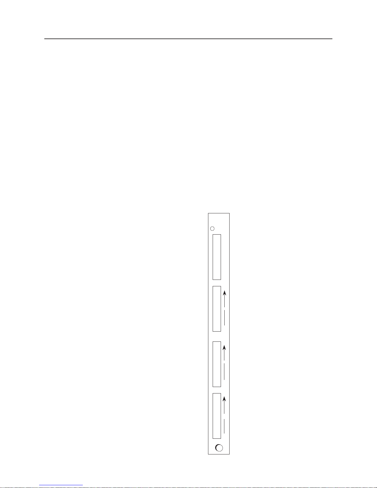
FRONT PANEL The LeCroy Module 3377 TDC front panel provides the user with
connectors for system integration and LEDs to assist system debugging.
Cables necessary for proper installation can be purchased from LeCroy.
See Section 3 for more information regarding cabling.
LeCroy
3377
TDC
N
T-O
WST
BSY
CLR
COM
WAK
GND
—
MPI
—
—
REN
PASS
+–
IN
15
GND
16
+–
IN
31
GND
1
+–
ECL
OUT
16
__
0
14
Page 12

Displays N LED: The only LED on the front panel is an N indicator, which is
illuminated whenever the module is addressed.
Termination LED: Just behind the front panel, between the lower input
connector and the ECL port, is an LED which is only visible when there
are no signal cables connected. The control signal terminations and pull
down resistors for the control signals and the ECL port are socketed.
When several 3377 are bussed together to a 4301 FERA driver, all of the
socketed resistors should be removed from each unit, except from the
last 3377. The termination LED uses one of the unused resistors in a
pull down resistor SIP and is lit when the SIP is installed. When several
3377s are bussed together only the last one should have this LED
illuminated.
Inputs and Outputs
Control Below the N LED is a 26 pin header used for ECL port control (WST,
WAK, REN, PASS), time out input (T-O), busy output (BSY), clear input
(CLR), common input (COM), and measure pause input (MPI).
■ T-O - Timeout input: A dECL input used to receive an external
common start timeout. The rising edge of this input ends acquisition
in common start mode. It is OR'ed with the internal time out.
■ WST - Write Strobe: dECL output indicates when a valid data word
is present on the ECLport.
■ BSY - Busy output: This dECL output indicates the 3377 cannot
accept hits. This occurs during the buffering dead time and when the
multievent buffer is full.
■ CLR - Clear input: A dECL input used to fast clear events and
abort acquisition or MTD133 readout. The control registers and data
from previous events is not affected.
■ COM - Common input: A dECL input for the common hit. The time
measurement is from the rising edge. Note: In Common Start
modes, additional pulses on the COM line arriving before the
Common Start timeout will disable acquisition.
■ WAK - Write Acknowledged: Input from 4301 or 4302 for FERA
interlocked handshake. Indicates that the data has been accepted.
■ GND - Ground
■ MPI - Measure Pause Interval: A dECL input for external MPI.
This is OR’ed with the internal MPI. The effect is to hold off unloading of the data from the MTD133s until the end of MPI.
■ REN - Readout Enable: dECL Input that enables the ECLbus
drivers and allows one event to be read out. REN must cycle false
and then true again for the next event to be read out.
■ PASS: A dECL output indicating that the last valid data word in the
current event has been read out.
15
Page 13

Signal Inputs Two 34 pin headers are for hit inputs; marked IN. The channels are
arranged sequentially from channel 0 at the top to channel 15 and
channel 16 to channel 31. The bottom pins (33,34) on both headers are
grounded through 100 ohm resistors. The hit inputs are dECL, polarity is
such that a positive going edge on the left hand (odd numbered) pin is
interpreted as the leading edge.
ECLbus output The bottom header is the ECLbus output port; marked ECL OUT. This
header is used for the FERA compatible readout.
REAR PANEL Located on the back of the unit is a twenty pin header which is the
trigger output for the unit. This connector is inverted so pin one is at the
bottom. The pins are grouped in pairs, with the bottom pair being the
first (pins 1 and 2).
Pair Function
1 (1,2) Trigger output 1, ch 0-3
2 (3,4) Trigger output 2, ch 4-7
3 (5,6) Trigger output 3, ch 8-11
4 (7,8) Trigger output 4, ch 12-15
5 (9,10) Trigger output 5, ch 16-19
6 (11,12) Trigger output 6, ch 20-23
7 (13,14) Trigger output 7, ch 24-27
8 (15,16) Trigger output 8, ch 28-31
9 (pins 17,18) Output disable (enabled when open)
10 (pins 19,20) External trigger clock input
STANDARD CAMAC
FUNCTION CODES F0, A0 Read FIFO data until end of event, Q=1 for valid data,
Q=0 at end
F0, A1 Read FIFO data always, (common start only)
F0, A2 Examine FIFO output, do not advance FIFO (common
start only)
F1, A0 Read Control register 0
F1, A1 Read Control register 1
F1, A2 Read Control register 2
F1, A3 Read Control register 3
F1, A4 Read Control register 4 (common start only)
F1, A5 Read Control register 5 (common start only)
F1, A6 Read CAMAC Test Register (common start only)
F8, A0 Test LAM
F9, A0 Clear all data and LAM. This does NOT affect the
control registers
F10, A0 Clear LAM
F16, A0 Write 16 bit data to FIFO (common start only)
F16, A1 Write FIFO tag bit (common start only)
F17, A0 Write Control register 0
F17, A1 Write Control register 1
F17, A2 Write Control register 2
16
Page 14

F17, A3 Write Control register 3
F17, A4 Write Control register 4 (common start only)
F17, A5 Write Control register 5 (common start only)
F24, A0 Disable LAM
F24, A1 Disable Acquisition mode
F25, A0 Initiate test cycle (common start only)
F26,A0 Enable LAM
F26, A1 Enable Acquisition mode
F27, A0 Test buffering in progress (BIP), Q=1 while BIP
F27, A1 Test busy, Q=1 while busy
F27, A2 Test event ready, Q=1 if event ready for readout
F27, A3 Test FIFO tag bit, Q=1 if tag bit set for word to be read
next
F30 Begin the reprogramming sequence
For completeness, we describe the following commands that are
available only during the programming mode of the Model 3377’s
internal Xilinx logic chip. These enable the mode to be set by selecting a
firmware program from the 4 that are installed in the EPROM, or loading
a different program from CAMAC. For these commands, the A lines are
not decoded, they are simply ignored.
F9 Clear data buffers, enable Xilinx program
F12 Test if Xilinx ready for data (Q=1 when ready)
F13 Test Xilinx programming done (Q=1 when done)
F14 Test Xilinx INIT signal
F16 Write 8 bits to Xilinx
F21 Select EPROM mode 1
F22 Select EPROM mode 2
F23 Select EPROM mode 3
F25 Begin Xilinx programming sequence
F28 Select CAMAC programming mode
F30 Enable Xilinx programming mode
(this resets the Xilinx, and selects EPROM mode 0)
17
Page 15

OPERATING INSTRUCTIONS
The 3377 has four separate operating modes. The mode is determined
by the Xilinx program loaded from the eprom, see below for changing
operating mode. The times are measured with respect to a common hit,
which can occur before or after the individual time signal to be measured
(Common Stop or Common Start mode). The other mode dependent
feature is the data format, which can be either single or double word. A
summary of the modes is listed below.
Mode Operation Data Format
0 Common Stop Single Word (Default Mode)
1 Common Start Single Word
2 Common Stop Double Word
3 Common Start Double Word
Since the features and control registers of the modes are quite different
in some cases, the control registers, data word formats, and operation of
the four different modes are discussed separately in the “Operating
Modes” section.
PROGRAMMING THE UNIT
FOR A DIFFERENT MODE
OF OPERATION When initially powered on, the module configures itself for Common
Stop, Single Word mode. The module is ready for the first command
approximately 200 milliseconds after power on. The first command
received by the module must be F9 for correct operation.
To change to any other mode the following sequence of CAMAC operations to the module is required:
1. F30, any subaddress. This selects programming mode and resets
the Xilinx gate array. The default program load is the Common Stop
mode, Single Word data format.
2. To select a program mode other than the default, perform an F21,
F22, or F23 CAMAC operation. To reprogram the Common Stop
Single Word mode, simply skip this step.
F21, any subaddress. This selects the common start, single word
program load.
F22, any subaddress. This selects the common stop, double word
program load.
F23, any subaddress. This selects the common start, double word
program load.
3. F25, any subaddress. This begins the programming of the Xilinx
chip, using the selected program load (or the default load). This will
take less than 200 milliseconds to complete.
19
Page 16

4. F13, any subaddress. Test the done flag, return Q=1 when programming is complete. The host computer should loop on this command
until Q is equal to 1.
5. F9, any subaddress. This is REQUIRED after reprogramming. This
resets the on board PAL (programmed array logic device) which
allows the Xilinx to be programmed, causing all function codes to be
ignored by the PAL, except for F30, which starts the reprogramming
sequence. The F9 command also MUST be the FIRST command
received by the module after power up, to ensure that the PAL has
been disabled.
After loading the Xilinx gate array, and performing the F9 command, the
Xilinx gate array takes control of the module. The new CAMAC function
codes which have been programmed into the gate array logic become
operational.
OPERATING MODES IMPORTANT NOTE: The control registers, header contents, data
word format, and trigger outputs are dependent on the mode
setting.
20
Page 17

Mode 0: Common Stop,
Single Word Mode
Control Registers
15 14 13 12 11 10 9 8 7 6 5 4 3 2 1 0
Mode
Edge Recording
Buffer Mode
Data Shift Value
Readout Mode
Header Mode
User settable ID Code
Control Register #1
15 14 13 12 11 10 9 8 7 6 5 4 3 2 1 0
Control Register #0
Serial number
FERA Mode
MPI
Trig. clock
unit
Trigger pulse
delay
Trigger Pulse Width
Control Register #2
15 14 13 12 11 10 9 8 7 6 5 4 3 2 1 0
Max. full scale time
Max. # Hits
Control Register #3
15 14 13 12 11 10 9 8 7 6 5 4 3 2 1 0
Offset
Mode 0 Control Registers
Request delay
control register 0 (subaddress 0)
bits 0-7 user definable module ID code. This appears in the
header data word. Default is 0.
bits 8-9 data shift value. This determines the TDC resolution.
0 = 0.5 nsec (default)
1 = 1.0 nsec
2 = 2.0 nsec
3 = 4.0 nsec
bit 10 Selects LEADING edge recording, or BOTH edges.
1 = Both edges are recorded
0 = Leading edge ONLY is recorded (default)
bit 11 Selects readout mode.
1 = ECL PORT (FERA mode)
0 = CAMAC readout (default)
bit 12 Selects Buffer mode
1 = Multi-event buffer mode
0 = Single buffer mode. In this mode the FERA
readout is compatible with the 4300B FERA
ADC. The request delay (see register 3) must
be set appropriately. (default)
bit 13 Selects Header mode
0 = always have header (default)
1 = skip header if no data words
21
Page 18

bit 14, 15 Read only, indicates the program load in use. Common
Stop Single Word mode is 0
control register 1 (subaddress 1)
bits 0-3 Selects the trigger output pulse width, in clock units, 0 to
15. Default is 0.
bits 4-7 Selects the trigger pulse delay, in clock units. The
maximum delay is 15 clock units. Default is 0.
bits 8-9 Selects the trigger clock unit.
0 = 25 nsec (default)
1 = 50 nsec
2 = 100 nsec
3 = selects external trigger clock
bit 10-11 Selects the Measure Pause Interval (MPI).
0 = no MPI (default)
1 = 800 nsec MPI
2 = 1600 nsec MPI
3 = 3200 nsec MPI
bit 12 Selects FAST FERA mode
1 = fast
0 = normal (default)
bit 13 - 15 Event serial number. This 3 bit number is in the header
data word. It is incremented after each event. It can be
written and read to allow synchronizing several modules. It
is cleared by CAMAC command F9. Default is 0.
control register 2 (subaddress 2)
bits 0-3 The maximum number of hits allowed per TDC channel,
from 1 to 16. A value of zero selects 16 hits. Default is 15.
bits 4-15 The maximum full scale time allowed for the TDC data, in
units of 8 nsec, from 0 to 32767.5 nsec. Bit 4 has a value
of 8 nsec. This value MUST be set correctly to limit the full
scale range to less than the range allowed by the
resolution and edge selection specified in register 0.
Default is full scale 32767.5 nsec
control register 3 (subaddress 3)
bits 0-3 The request delay setting. This is used only in 4300B
FERA ADC compatible mode. The range is from 0 to
30 microseconds, in 2 microsecond steps. In this mode
the BUSY output becomes the FERA REQUEST output.
Default is 0.
22
Page 19

bits 4-15 The Offset to be subtracted from the data before shifting
and readout, in units of 8 nsec. Bit 4 has a value of
8 nsec. This value must be set in a manner consistent with
the setting of the maximum time range in register 2.
Default is 0.
A simple example of Common STOP register setup:
0 = 10FFH buffered mode, CAMAC readout, leading edge only,
0.5 nsec resolution, header always, module ID is 255
1 = 00FFH event numbers starts at zero, no MPI, 25 nsec trigger
clock, maximum trigger width and delay
2 = 03F0H full scale is 511 nsec, 16 hits allowed
3 = 0000H zero offset, and no request delay (not used in buffered
mode)
Maximum Time Range The maximum time range is implemented inside the MTD133 monolithic
integrated circuit. The range is from 15 counts (7.5 nsec) to 65535
counts (32767.5 nsec). Any data which is GREATER THAN the maximum time range is discarded inside the MTD133 and exacts no readout
time penalty. Any data which is EQUAL TO or LESS THAN the maximum
time range can be readout.
The maximum time range is set in register 2. Only the upper 12 bits of
the 16 bit word are used for the maximum time range. These 12 bits are
compared to the upper 12 bits of the data words inside the MTD133. The
lower 4 bits are ignored by the hardware inside the MTD133. The
maximum data value which can be readout is equal to the maximum
time range value + 15 counts, or a multiple of 8 nsec +7.5 nsec. A value
of zero (for the upper 12 bits) allows readout of all data words of 15
counts (7.5 nsec) or less.
Offset The Offset register is implemented on the 3377 board, in the program-
mable gate array chip. Only the upper 12 bits of this 16 bit word can be
set. The lower 4 bits are effectively set to zero. The offset is subtracted
from the data read from the MTD133, before the shift is applied. If the
data is GREATER THAN or EQUAL to the offset, the result of the
subtraction is then shifted (to choose the resolution) and becomes the
data to be stored in the FIFO buffer. If the data is LESS THAN the offset,
the data is discarded and no data word is stored.
It is possible to implement a time window, using the maximum time
range as the upper end and the offset value as the lower end. The upper
end is the maximum time range setting + 7.5 nsec. The lower end is the
offset value. These two values must be set properly for the resolution
and edge mode selected, or the data will be ambiguous. The offset must
be less than the maximum time range, and greater than or equal to the
23
Page 20

[(maximum time range setting + 15) - difference], where difference is from
the table below.
Resolution Edge Mode Difference
0.5 nsec leading edge only 1023
both edges 511
1.0 nsec leading edge only 2047
both edges 1023
2.0 nsec leading edge only 4095
both edges 2047
4.0 nsec leading 8191
both edges 4095
For 2 nsec resolution and both edge mode, the difference is 2047. For an
offset of 512 nsec (a multiple of 8 nsec), the maximum time range value
should be 1528 nsec (also a multiple of 8 nsec). There are 512 possible
data values, from 0 to 1022 nsec. A raw data value of 512 through 513.5
nsec will be readout as zero, the raw data value of 1534 through 1535.5
nsec will be read out as 1022 nsec.
NOTE: Any data which occurs between the lower bound of the window
and the common STOP will still be recorded, and will occupy storage
space in the MTD133 chip. If a time window is used, it is recommended to
set the maximum number of hits to 16, and that the offset value be small.
Dead Time The 3377 is a pipelined TDC, and the pipeline is stopped during the
transfer of the hit data from the chips to the FIFO event buffer on the
board. The time to buffer the data is typically 1.8 µs + 100 nsec per hit.
During this time the front panel BUSY output is asserted and the module
responds with Q=1 to an F27, A1 command. Any inputs received at the
front panel will be ignored during this period. Only when buffering of the
data is complete and the BUSY is turned off is the module ready to
receive data at the front panel signal inputs.
The trigger system must wait for the pipeline to refill before sending a new
common stop signal. This refill time should be equal to the maximum time
range selected in register 2. It is the responsibility of the trigger system to
provide this delay. If a common stop is received before the pipeline has
completely refilled (before the maximum time has passed), then valid hits
that occurred within the maximum time range, but during the dead time,
will not be recorded. If the 3377 is not set to buffer the data then busy will
remain on until the data is read out of the unit.
Front Panel Clear Input This input is used to clear an event in progress. The CLEAR is effective
ONLY between the COMMON STOP and the end of MPI “Measured Pulse
Interval (MPI)”. If MPI is set to 0, the CLEAR is ignored. To be reliable, the
CLEAR must arrive at least 100 nsec AFTER the leading edge of the
COMMON STOP, and at least 100 nsec BEFORE the end of MPI (COMMON STOP time plus the MPI setting). The CLEAR signal is synchronized
internally with the 100 nsec system clock, and its behavior exhibits 100
nsec of jitter due to the random phase of this clock with respect to the
external input signals.
24
Page 21

Mode 1: Common Start, Single Word
Control Register
15 14 13 12 11 10 9 8 7 6 5 4 3 2 1 0
Control Register #0
User settable ID
code
Mode
Edge Recording
Buffer Mode
Data Shift Value
Readout Mode
Header Mode
15 14 13 12 11 10 9 8 7 6 5 4 3 2 1 0
Serial number
MPI
FERA Mode
Not used
Control Register #2
Control Register #1
15 14 13 12 11 10 9 8 7 6 5 4 3 2 1 0
Not used
Max. hits
Control Register #3
15 14 13 12 11 10 9 8 7 6 5 4 3 2 1 0
Enforced Common Start Time Out
Request delay
Control Register #4
15 14 13 12 11 10 9 8 7 6 5 4 3 2 1 0
Not used
Common Start Timeout
Control Register #5
15 14 13 12 11 10 9 8 7 6 5 4 3 2 1 0
Not Used
Test Enable
Not
used
Test mode
clock
Number of test
pulses
Mode 1 Control Registers
control register 0 (subaddress 0)
bits 0-7 user definable module ID code. This appears in the `
header data word.
bits 8-9 data shift value. This determines the TDC resolution.
0 = 0.5 nsec
1 = 1.0 nsec
2 = 2.0 nsec
3 = 4.0 nsec
bit 10 Selects LEADING edge recording, or BOTH edges.
1 = Both edges are recorded
0 = Leading edge ONLY is recorded
bit 11 Selects readout mode.
1 = ECL PORT (FERA mode)
0 = CAMAC readout
25
Page 22

bit 12 Selects Buffer mode
1 = Multi-event buffer mode
0 = Single buffer mode. In this mode the FERA
readout is compatible with the 4300B FERA ADC.
The request delay (see register 3) must be set
appropriately.
bit 13 Selects Header mode
0 = always have header (default)
1 = skip header if no data words
bit 14, 15 Read only, indicates the program load in use. Common
Start mode is 1
control register 1 (subaddress 1)
bits 0-9 not used, always read 0.
bit 10-11 Selects the Measure Pause Interval (MPI).
0 = no MPI
1 = 800 nsec MPI
2 = 1600 nsec MPI
3 = 3200 nsec
bit 12 MPI Selects FAST FERA mode,
1 = fast
0 = normal
26
bit 13 - 15 Event serial number. This 3 bit number is in the header
data word. It is incremented after each event. It can be
written and read to allow synchronizing several modules.
It is cleared by CAMAC command F9.
control register 2 (subaddress 2)
bits 0-3 The maximum number of hits allowed per TDC 16 hits.
bits 4-15 Not used, always read 1
control register 3 (subaddress 3)
bits 0-3 The request delay setting. This is used only 4300B FERA
ADC compatible mode. The range is from 0 to
30 microseconds, in 2 microsecond steps. In this mode
the BUSY becomes the FERA request output
bits 4-15 The maximum time range for the data, tested before
shifting and readout, in units of 8 ns. Bit 4 has a value of
8 ns. This enforces a precise common start time out
control register 4 (subaddress 4)
bits 0-9 The Common start time out value in units of 50 nsec, up
to 32 microseconds. The minimum delay is about
25 nsec, for a setting of 0. The actual value jitters
50 nsec due to the synchronization with the internal
50 nsec clock. This MUST be set to a value LESS THAN
full scale (32,767.5 microseconds).
Page 23

bits 10-15 Not used, always reads 0
control register 5 (subaddress 5)
bits 0-4 The number of pulses generated in test mode. 0-31
pulses, each 1/2 clock period long.
bits 5-6 The test mode clock.
0 = 100 nsec
1 = 200 nsec
2 = 400 nsec
3 = 800 nsec
bit 7 Not used, always reads 0
bit 8 Test enable. This must be 1 for test mode.
bits 9-15 Not used, always reads 0.
A simple example of Common START register setup
0 = 10FFH buffered mode, CAMAC readout, leading edge only,
0.5 nsec resolution, header always, module ID is 255
1 = 0000H event numbers starts at zero, no MPI
2 = 0000H 16 hits allowed
3 = 03F0H time out enforced at 511 nsec, no request delay (not used
in buffered mode)
4 = 000BH time out at 550 nsec, slightly longer than the enforced
time out delay
5 = 0000H test mode NOT selected
Common Start Time Out A precise common start time out is enforced in steps of 8 nsec by the
value in control register 3, bits 4-15. The raw data value is compared to
this value. Any data value GREATER THAN or EQUAL TO the timeout
value will be discarded. Only data LESS THAN the timeout will be read
out. This value MUST be consistent with the resolution and edge mode
chosen, or the data will be ambiguous. The Common Start Timeout
value must be less than that given in the table below.
Resolution Edge Mode Time Out Value
0.5 nsec leading edge only 1024
both edges 512
1.0 nsec leading edge only 2048
both edges 1024
2.0 nsec leading edge only 4096
both edges 2048
4.0 nsec leading edge only 8192
both edges 4096
27
Page 24

The common start time out value from register 4 controls the end of
acquisition in steps of 50 nsec, with a 50 nsec jitter due to clock
synchronization. This value should be set to result in a minimum time out
slightly longer than the value specified in register 3. If the external
common stop time out is used, there is no synchronization jitter, and the
coincidence resolution can be set precisely.
For example, with 2 nsec resolution and leading edge mode, the maximum time can be as large as 2046 nsec. The time out should be set to
41 (2050 nsec), and the offset value to 2048. This allows use of the full
available range.
NOTE: Any data which occurs after the enforced Common Start timeout
time, but before the actual end of acquisition (the common start time out)
will still be recorded. This data will occupy storage space in the MTD133
chip. It is recommended to set the maximum number of hits to a value
slightly higher than the number expected.
Dead Time After the common start time out the 3377 buffers the data. Buffering
takes typically 1.8 µs +100 nsec per hit. During this time the front panel
BUSY output is asserted and the module responds with Q=1 to an F27,
A1 command. Any inputs received at the front panel will be ignored
during this period. Only when buffering of the data is complete and the
BUSY is turned off is the module ready to receive data at the front panel
signal inputs. The module is now ready for a new event, beginning with
the common hit. If the 3377 is not set to buffer (see section “Buffered
Mode”) then busy will remain on until the data is read out of the unit.
Front Panel Clear This input is used to clear an event in progress. The CLEAR signal is
synchronized internally with the 100 nsec system clock, and its behavior
exhibits 100 nsec of jitter due to the random phase of this clock with
respect to the external input signals.
The CLEAR is effective from COMMON START to the end of MPI. If
MPI is set to 0, then CLEAR is effective from COMMON START to the
COMMON START TIME OUT. Note that the COMMON START TIME
OUT period is effectively an ‘MPI’. Note that CLEAR is ALWAYS permitted during the COMMON START TIME OUT period. To be reliable, the
CLEAR must arrive at least 100 nsec AFTER the leading edge of the
COMMON START, and at least 100 nsec BEFORE the COMMON
START TIME OUT or the end of MPI (COMMON START TIME OUT plus
the MPI setting).
28
Page 25

Mode 2: Common Stop, double word
Control Registers There are only 4 control registers
Control Register #0
15 14 13 12 11 10 9 8 7 6 5 4 3 2 1 0
Edge Recording
Buffer Mode
Mode
Control Register #1
15 14 13 12 11 10 9 8 7 6 5 4 3 2 1 0
Not used
Readout Mode
Header Mode
User settable ID
code
Serial number
FERA Mode
MPI
Trig. clock
unit
Trigger pulse
delay
Trigger out pulse
Control Register #2
15 14 13 12 11 10 9 8 7 6 5 4 3 2 1 0
Max. full scale time
Max. hits
Control Register #3
15 14 13 12 11 10 9 8 7 6 5 4 3 2 1 0
Not Used
Mode 2 Control Registers
Request delay
control register 0 (subaddress 0)
bits 0-7 user definable module ID code. This appears in the
header data word. The default is 0.
bits 8-9 Not used, always read 0
bit 10 Selects LEADING edge recording, or BOTH edges.
1 = Both edges are recorded
0 = Leading edge ONLY is recorded (default)
bit 11 Selects readout mode.
1 = ECL PORT (FERA mode)
0 = CAMAC readout (default)
bit 12 Selects Buffer mode
1 = Multi-event buffer mode
0 = Single buffer mode. In this mode the FERA
readout is compatible with the 4300B FERA ADC.
The request delay (see register 3) must be set
appropriately. (default)
bit 13 Selects Header mode
0 = always have header (default)
1 = skip header if no data words
29
Page 26

bit 14, 15 Read only, indicates the program load in use. Common
Stop Double Word mode is 2
control register 1 (subaddress 1)
bits 0-3 Selects the trigger output pulse width, in clock units, 0 to
15. Default is 0.
bits 4-7 Selects the trigger pulse delay, in clock units. The
maximum delay is 15 clock units. Default is 0.
bits 8-9 Selects the trigger clock unit.
0 = 25 nsec (default)
1 = 50 nsec
2 = 100 nsec
3 = selects external trigger clock
bit 10-11 Selects the Measure Pause Interval (MPI).
0 = no MPI (default)
1 = 800 nsec MPI
2 = 1600 nsec MPI
3 = 3200 nsec MPI
bit 12 Selects FAST FERA mode; 1=fast 0=normal (default)
bit 13 - 15 Event serial number. This 3 bit number is in the header
data word. It is incremented after each event. It can be
written and read to allow synchronizing several modules.
It is cleared by CAMAC command F9. Default is 0.
control register 2 (subaddress 2)
bits 0-3 The maximum number of hits allowed per TDC channel,
from 1 to 16. A value of zero selects 16 hits. Default is 15.
bits 4-15 The maximum full scale time allowed for the TDC data, in
units of 8 nsec, from 0 to 32767.5 nsec. Bit 4 has a value
of 8 nsec.
control register 3 (subaddress 3)
bits 0-3 The request delay setting. This is used only in 4300B
FERA ADC compatible mode. The range is from 0 to
30 microseconds, in 2 microsecond steps. In this mode
the BUSY output becomes the FERA REQUEST output.
Default is 0.
bits 4-15 Not used, always read 0.
A simple example of Common STOP register setup
30
0 = 10FFH buffered mode, CAMAC readout, leading edge only,
header always, module ID is 255
Page 27

1 = 00FFH event numbers starts at zero, no MPI, 25 nsec trigger
clock, maximum trigger width and delay
2 = 4E20H full scale is 10 µsec, 16 hits allowed
3 = 0000H no request delay (not used in buffered mode)
Maximum time range The maximum time range is implemented inside the MTD133 monolithic
integrated circuit. The range is from 15 counts (7.5 nsec) to 65535
counts (32767.5 nsec). Any data which is GREATER THAN the maximum time range is discarded inside the MTD133 and exacts no readout
time penalty. Any data which is EQUAL TO or LESS THAN the maximum time range can be readout.
The maximum time range is set in register 2. Only the upper 12 bits of
the 16 bit word are used for the maximum time range. These 12 bits are
compared to the upper 12 bits of the data words inside the MTD133. The
lower 4 bits are ignored by the hardware inside the MTD133. The
maximum data value which can be readout is equal to the maximum
time range value + 15 counts, or a multiple of 8 nsec +7.5 nsec. A value
of zero (for the upper 12 bits) allows readout of all data words of 15
counts (7.5 nsec) or less.
Dead Time The 3377 is a pipelined TDC, and the pipeline is stopped during the
transfer of the hit data from the chips to the FIFO event buffer on the
board. The time to buffer the data is typically 1.8 µs + 200 nsec per hit.
During this time the front panel BUSY output is asserted and the module
responds with Q=1 to an F27, A1 command. Any inputs received at the
front panel will be ignored during this period. Only when buffering of the
data is complete and the BUSY is turned off is the module ready to
receive data at the front panel signal inputs.
The trigger system must wait for the pipeline to refill before sending a
new common stop signal This refill time should be equal to the maximum time range selected in register 2. It is the responsibility of the
trigger system to provide this delay. If a common stop is received before
the pipeline has completely refilled (before the maximum time has
passed), then valid hits that occurred within the maximum time range,
but during the dead time will not be recorded.
If the 3377 is set to single buffer mode (see section “Unbuffered Mode”)
then busy will remain on until the data is read out of the unit.
Front Panel Clear Input This input is used to clear an event in progress. The CLEAR is effective
ONLY between the COMMON STOP and the end of MPI. If MPI is set to
0, the CLEAR is ignored. To be reliable, the CLEAR must arrive at least
100 nsec AFTER the leading edge of the COMMON STOP, and at least
100 nsec BEFORE the end of MPI (COMMON STOP time plus the MPI
setting). The CLEAR signal is synchronized internally with the 100 nsec
system clock, and its behavior exhibits 100 nsec of jitter due to the
random phase of this clock with respect to the external input signals.
31
Page 28

Mode 3: Common Start, Double Word Mode
Control Registers CONTROL REGISTERS, COMMON START, DOUBLE WORD MODE
There are 6 control registers.
Control Register #0
15 14 13 12 11 10 9 8 7 6 5 4 3 2 1 0
Edge Recording
Buffer Mode
Mode
Not Used
Readout Mode
Header Mode
Control Register #1
15 14 13 12 11 10 9 8 7 6 5 4 3 2 1 0
User settable ID
code
Serial number
MPI
FERA Mode
Not used
Control Register #2
15 14 13 12 11 10 9 8 7 6 5 4 3 2 1 0
Not Used
Max. hits
Control Register #3
15 14 13 12 11 10 9 8 7 6 5 4 3 2 1 0
Not Used
Request delay
Control Register #4
15 14 13 12 11 10 9 8 7 6 5 4 3 2 1 0
Not used
Common Start Timeout
Control Register #5
15 14 13 12 11 10 9 8 7 6 5 4 3 2 1 0
Not Used
Test Enable
Not
used
Test mode
clock
Number of test
pulses
Mode 3 Control Registers
control register 0 (subaddress 0)
bits 0-7 user definable module ID code. This appears in the
header data word.
32
bits 8-9 Not used, always read 0.
bit 10 Selects LEADING edge recording, or BOTH edges.
1 = Both edges are recorded
0 = Leading edge ONLY is recorded
bit 11 Selects readout mode.
1 = ECL PORT (FERA mode)
0 = CAMAC readout
bit 12 Selects Buffer mode
1 = Multi-event buffer mode
0 = Single buffer mode. In this mode the FERA
readout is compatible with the 4300B FERA ADC.
The request delay (see register 3) must be set
appropriately.
Page 29

bit 13 Selects Header mode 0 = always have header (default)
1 = skip header if no data words
bit 14, 15 Read only, indicates the program load in use.
Common Start Double Word mode is 3
control register 1 (subaddress 1)
bits 0-10 Not used, always reads 0.
bit 10-11 Selects the Measure Pause Interval (MPI).
0 = no MPI
1 = 800 nsec MPI
2 = 1600 nsec MPI
3 = 3200 nsec MPI
bit 12 Selects FAST FERA mode, 1=fast, 0=normal
bit 13 - 15 Event serial number. This 3 bit number is in the header
data word. It is incremented after each event. It can be
written and read to allow synchronizing several modules.
It is cleared by CAMAC command F9.
control register 2 (subaddress 2)
bits 0-3 The maximum number of hits allowed per TDC channel,
from 1 to 16. A value of zero selects 16 hits.
bits 4-15 Not used, always reads 1
control register 3 (subaddress 3)
bits 0-3 The request delay setting. This is used only in 4300B
FERA ADC compatible mode. The range is from 0 to
30 microseconds, in 2 microsecond steps.
bits 4-15 Not used, always read 0.
control register 4 (subaddress 4)
bits 0-9 The Common start time out value in units of 50 nsec, up
to 32 microseconds. The minimum delay is about
25 nsec, for a setting of 0. The actual value jitters 50 nsec
due to the synchronization with the internal 50 nsec clock.
This MUST be set to a value LESS THAN full scale
(32767.5 microseconds).
bits 10-15 Not used, always reads 0
control register 5 (subaddress 5)
bits 0-4 The number of pulses generated in test mode. 0-31
pulses, each 1/2 clock period long.
33
Page 30

bits 5-6 The test mode clock
0 = 100 nsec
1 = 200 nsec
2 = 400 nsec
3 = 800 nsec
bit 7 Not used, always reads 0
bit 8 Test enable. This must be 1 for test mode.
bits 9-15 Not used, always reads 0.
A simple example of Common START register setup
0 = 10FFH buffered mode, CAMAC readout, leading edge only,
header always, module ID is 255
1 = 0000H event numbers starts at zero, no MPI
2 = 0000H 16 hits allowed
3 = 0000H no request delay (not used in buffered mode)
4 = 00C8H time out at 10 microseconds.
5 = 0000H test mode NOT selected
Common Start Time Out The internal common start time out value selected in register 4 controls
the end of acquisition in steps of 50 nsec, with a 50 nsec jitter due to
clock synchronization. If the external common stop time out is used,
there is no synchronization jitter, and the coincidence resolution can be
set precisely.
Dead Time After the common start time out the 3377 buffers the data. Buffering
takes typically 1.8 µs +200 nsec per hit. During this time the front panel
BUSY output is asserted and the module responds with Q=1 to an F27,
A1 command. Any inputs received at the front panel will be ignored
during this period. Only when buffering of the data is complete and the
BUSY is turned off is the module ready to receive data at the front panel
signal inputs. The module is now ready for a new event, beginning with
the common hit. If the single buffer mode is selected (see section
“Unbuffered Mode”) then busy will remain on until the data is read out of
the unit.
Front panel Clear This input is used to clear an event in progress. The CLEAR signal is
synchronized internally with the 100 nsec system clock, and its behavior
exhibits 100 nsec of jitter due to the random phase of this clock with
respect to the external input signals.
34
The CLEAR is effective from COMMON START to the end of MPI. If MPI
is set to 0, then CLEAR is effective from COMMON START to the
COMMON START TIME OUT. Note that the COMMON START TIME
OUT period is effectively an ‘MPI’. Note that CLEAR is ALWAYS permitted during the COMMON START TIME OUT period. To be reliable, the
Page 31

CLEAR must arrive at least 100 nsec AFTER the leading edge of the
COMMON START, and at least 100 nsec BEFORE the COMMON
START TIME OUT or the end of MPI (COMMON START TIME OUT plus
the MPI setting).
35
Page 32

TRIGGER OUTPUTS
Trigger Outputs in the
Common Stop Modes The eight prompt OR outputs are stretched (one shots) and delayed
(pipeline delay) using digital techniques. The trigger output pulse width
and delay can be selected, in increments as small as 25 nsec. The
output pulses have a jitter with respect to the input of up to 1 clock
period. This is due to the synchronous digital one shot and delay line
implemented in the gate array chip. The trigger outputs are latched for
the duration of the MPI signal, which begins at the common STOP time.
If MPI is set to zero, no latching takes place.
The leading edge of the OR of 4 inputs asynchronously triggers a digital
one shot. The width is selected from 1 to 16 clock periods. The clock is
selected from 10, 20 and 40 MHz (25 nsec to 100 nsec period), or an
external clock which must be less than 40 MHz. The differential ECL
external clock input is on the trigger connector, pins 19 and 20. The one
shot is retriggerable after one full clock period after the input trigger. If a
second trigger arrives during an output pulse, the output pulse is
extended.
The pipeline delay is adjustable from 0 to 15 clock periods, using the
same clock as the one shot. If zero delay is selected the outputs have
the same leading edge time as the OR, but the width displays the jitter
due to the clock. If a non zero delay is selected, both the leading and
trailing edges are synchronized with the clock, not with the input.
The trigger output data path includes a transparent latch. These latches
are transparent during normal acquisition and are latched by the MPI
(measure pause interval) which has the leading edge time of the common STOP input. The outputs remain latched until the end of MPI. If the
MPI is set to 0 (no MPI) then the latches remain transparent
36
Page 33

This system enables the experimenter to latch the state of all OR
outputs as they existed during the actual event time, even if the common
STOP arrives somewhat later than the end of the event time. The width
should be set to the desired coincidence resolution (the drift time of the
chamber). If the trigger outputs of several 3377 modules are to be
combined in a trigger system, an appropriate external clock should be
supplied to synchronize the trigger outputs. Otherwise the trigger
coincidence resolution must be increased to cover the random phase of
the clocks in each 3377 module.
Trigger Outputs in the
Common Start Modes The eight prompt OR outputs are used as the clock input to flip flops
which are enabled by the common START signal, and disabled by the
end of acquisition (the common start time out). Any signal inputs during
this interval set the flip flop and are latched. Signals which arrive before
the common START or after the time out, are ignored. The latches are
not reset until the end of readout (when the system returns to acquisition
mode). A fast clear during the MPI will also clear the latches. If the
external common stop time out is used, there is no synchronization jitter,
and the coincidence resolution can be set precisely.
37
Page 34

READOUT MODES AND DATA FORMATS
CAMAC
Buffered Mode This is the recommended CAMAC mode. With single word output
format, the multievent buffer will hold up to 8 full size events (512 data
words + header for each event). In double word format the buffer will
hold 4 events (1024 data words + header for each event), or up to 31
smaller events. The limit is 4095 words in the FIFO. The FIFO can
actually hold up to 8192 words, however no more events will be
accepted after the half full flag is turned on.
CAMAC readout is on an event by event basis, using F0, A0. A Q=1 is
returned if the data is valid. After the last data word for that event has
been read, the next F0, A0 always returns Q = 0. If another event is
waiting to be read the next F0, A0 will return the header word for the
next event with Q = 1, otherwise the module will continue to return Q=0.
Unbuffered mode The only difference is the behavior of the BUSY signal on the front panel
(and tested with F27, A1). Normally, the BUSY becomes true when the
common stop or common start time out is received, and remains on only
until the data is stored in the FIFO. In unbuffered mode, the BUSY is
delayed by the request delay setting (register 3), and remains true until
the data has been read from the module (the FIFO is empty again).
ECLPORT (FERA) mode
Buffered mode The behavior of the data and the BUSY signal is the same as for
CAMAC readout. This mode is NOT COMPATIBLE with 4300B FERA
ADC modules. The ECLbus must consist only of 3377 (or 3377 compatible modules). Standard FERA modules may not be intermixed.
Unbuffered mode This mode IS COMPATIBLE with the original FERA modules. The 4300B
ADC modules must be installed first in the ECLbus (closer to the 4301
FERA driver). The BUSY signal now becomes the REQ line in the FERA
control bus. The request delay should be set to a value such that it
comes on after the 4300B REQ signal, but before the 4300B can finish
reading out. This mode should be used only for 4300B compatibility. If
compatibility is not required, the buffered mode should be used.
FERA COMPATIBILITY Beginning with ECO #1101, the Model 3377 time digitizer has improved
compatibility with the Model 4300B FERA ADC. This change involves
firmware only, and is compatible with all production circuit boards (rev
A&B).
With this change, the REN signal can be used as flow control for the
ECLport output in the same way as the 4300, when the 3377 is in
unbuffered mode. In addition, a new mode has been provided which
allows the use of WAK for flow control when the 3377 ECLport is operated in the fast mode. The improved compatibility is summarized below.
Standard 4300B
FERA Behavior Conversion begins when a gate is received by the 4300B ADC module.
38
After the conversion is finished all modules which have data to be read
out assert the REQ line. REQ continues to be asserted until that module
Page 35

has been completely read out. The wire ORed REQ lines are received by
the 4301 driver which waits for an adjustable delay (up to 0.5 microsecond to be sure that all 4300Bs have finished conversion), then sends
REN to the first 4300B on the ECLbus. The data is then handshaked out
to the ECLbus using WST and WAK. After all data has been sent, REQ is
removed and PASS becomes a copy of REN.
If the first 4300 has not asserted REQ (there was no data above the
sparse scan threshold), then REN is simply copied to PASS. It is critical
that REN not be asserted until all 4300Bs have finished conversion,
because while REQ is not asserted, REN is simply copied to PASS.
If WST and WAK are used in the standard handshake mode, they control
the data flow. However, for high speed pipelined readout, WAK can be
jumpered to WST using the WSO and WAI connectors on the 4301
driver, effectively bypassing the handshake. The maximum ECLport rate
is achieved this way. In this case REN is used as the flow control.
Dropping REN effectively pauses the data flow. This works fine for the
4300B since there is only one data buffer. When REN returns, the data
flow resumes.
Modified Model 3377
FERA Behavior The 3377 TDC begins conversion after the end of acquisition, after the
common stop or the common start time out. The conversion time is not
fixed however, it depends on the amount of data and the mode (single or
double word). The conversion time can be as short as two microseconds
or as long as 103 microseconds. In addition, the 3377 has a multi event
buffer, which can hold as many as 31 events. Fortunately, the 3377 can
also be operated in an unbuffered mode, which although slightly different
than the 4300B FERA ADC, is quite compatible with it.
In the multi buffer mode, REN is used as a token to read out one event
from each 3377. As soon as conversion starts, BUSY (REQ) is asserted.
BUSY is removed as soon as the event is safely stored in the buffer. If
REN arrives before conversion is complete (and no previous event is
waiting in the buffer) the module simply waits for an event to become
ready. When the event has been completely read out, PASS is asserted
and the module waits for REN to become false. Then PASS is set false
and the module is ready to read out the next event in the buffer. This
ensures that each event is read out completely before any part of the
next event is read. This use of REN as an event token is incompatible
with the use as a flow control device in the 4300B FERA system. Note
that REN can be asserted even before the event, the module simply
waits for the event.
4300B Compatible Mode The single buffer mode is compatible with 4300Bs on the same ECLbus.
In this mode the BUSY signal becomes REQ. REQ can be delayed in
2 microsecond steps from 2 to 30 microseconds after the end of acquisition (the common stop, or the common start time out). REQ must not
come on before any 4300Bs on the ECLbus have finished conversion
and decided whether or not to assert REQ. REQ stays on until the data
has been read from the module. If REN arrives before conversion is
complete, the module waits for the event. During readout REN can be
used as flow control. After readout (and until the next conversion begins)
REN is simply copied to PASS. This allows REN to be used as flow
39
Page 36

control for modules later on the ECLbus. Note that 4300Bs and 3377s
can be arranged in any order on the ECLbus.
Fast FERA Mode The 3377 has 2 FERA modes, normal and fast. These are available both
in multi event buffered and single buffer modes. In normal FERA mode,
flow control is automatic, and uses the WST-WAK handshake. A fast
FERA mode can be selected by setting a bit in a control register, which
allows readout at 10 Mwords per second by ignoring the handshake. The
WST to WAK jumper is not required, so WAK is available for use as flow
control. Asserting WAK causes data readout to pause after the current
word. Readout will resume when WAK is removed. Note that the use of
WAK for flow control is not currently supported by the 4301 FERA driver
module (except as part of the WST-WAK handshake).
DATA FORMATS The 3377 output data is in either single or double word format. These
formats are identical for Common Start or Common Stop operation, and
for CAMAC or ECLbus readout.
Single Word Format The output data consists of a header word, followed by up to 512 data
words. An event with no data consists of only the header word. If header
suppression is selected, an event with no data results in zero words.
HEADER
bits 0-7 the 8 bit module ID (from register 0)
bits 8-9 the 2 bit resolution value (from register 0)
bit 10 the leading/both edge recording bit (from register 0).
0 = leading only 1 = both
bits 11-13 the event serial number, modulo 8
bit 14 always 0, identifies single word readout
bit 15 always 1, identifies header word
DATA WORD, leading edge only recording
bits 0-9 10 bit data value
bits 10-14 5 bit channel number
bit 15 always 0, identifies data word
DATA WORD, leading edge AND trailing edge recording
bits 0-8 9 bit data value
bit 9 Identifies the edge, 0 = leading, 1 = trailing
bits 10-14 5 bit channel number
bit 15 always 0, identifies data word
Double Word Format The output data consists of a header word, followed by up to 1024 data
words. An event with no data consists of only the header word. If header
suppression is selected, an event with no data results in zero words.
40
HEADER
bits 0-7 the 8 bit module ID (from register 0)
bits 8-9 the 2 bit resolution value, always 0
Page 37

bit 10 the leading/both edge recording bit (from register 0).
0 = leading only, 1 = both
bits 11-13 the event serial number (modulo 8)
bit 14 always 1 (identifies double word readout)
bit 15 always 1, identifies header word
FIRST DATA WORD
bits 0-7 8 bit data value
bit 8 1, indicates that the data is the most significant byte.
bit 9 Identifies the edge, 0 = leading, 1 = trailing
bits 10-14 5 bit channel number
bit 15 always 0, identifies data word
SECOND DATA WORD
bits 0-7 8 bit data value
bit 8 0, indicates that the data is the least significant byte.
bit 9 identifies edge, 0 = leading, 1 = trailing
bits 10-14 5 bit channel number
SUPPRESSING THE
HEADER The Header mode bit, register 0, bit 13, when set to 1, allows suppress-
ing the header word if there is no data in the event. This is effective in all
readout modes, single or double word, buffered or unbuffered, CAMAC
or FERA. The event is not suppressed, only the header, so the event
ordering remains correctly synchronized among multiple 3377 modules.
If the channel occupancy is low, the use of this feature can result in a
reduction in the size of the data block for each event, and a small decrease in readout time (not the same as the dead time). It is recommended that the last module in a readout group be set to always supply
the header (bit 13 set to 0).
41
Page 38

EXAMPLE 3377
PROGRAMMING SEQUENCE
Step 1: CAMAC Reprogramming (see Operating Instructions)
F9, any subaddress (should be executed as first command after powerup)
F30, any subaddress (selects programming mode, resets Xilinx chip)
F21, any subaddress (selects common start, single word mode)
F25, any subaddress (begins reprogramming of Xilinx chip)
Wait 500 ms for programming to finish (actual time: < 200 ms)
F13, any subaddress (check programming complete)
F9, any subaddress (reset PAL)
Step 2: Initialize module (for Common Start example)
F17 A0, data = 0x10FF
F17 A1, data = 0x0000
F17 A2, data = 0x0000
F17 A3, data = 0x03F0
F17 A4, data = 0x000B
F17 A5, data = 0x0101
F1 A0 (read back register 0 to check)
F1 A1 (read back register 1 to check)
F1 A2 (read back register 2 to check)
F1 A3 (read back register 3 to check)
F1 A4 (read back register 4 to check)
F1 A5 (read back register 5 to check)
F26 A0 (Enable LAM)
Step 3: Enable Acquisition Mode
F26 A1
Step 4: Execute Test Cycle
F25 A0
Step 5: Test Event Ready to Readout
F27 A2
Step 6: Read back data
F0 A0 (read data until Q=0)
42
Page 39

THEORY OF OPERATION
The Model 3377 time digitizer consists of 7 major subsystems:
TIME MEASUREMENTS Four LeCroy MTD133 custom monolithic integrated circuits perform the
actual time measurements. The 250 MHz clock is provided by a crystal
oscillator, and a symmetrizing circuit which adjusts the duty factor to
50%. The MTD133 uses a synchronous counter which counts on both
clock edges, giving an effective counting rate of 500 MHz. A four stage
delay line interpolator divides the counting period into 500 picosecond
intervals. A phase locked loop using an external op amp in the feedback
circuit adjusts the delay line to be exactly 2 nsec long. When an input
occurs, the grey coded counter and interpolator are latched and stored
in the LIFO.
Each MTD133 contains 8 input channels, each with 16 words of LIFO
storage. Both the depth of the storage, and the maximum time range are
programmable. The data is stored in the LIFO in a grey code format.
When the data is read out, the grey code is converted to binary, the
Common hit time is subtracted, and the time difference is compared to
the maximum time. This is done in a 3 stage pipeline to increase the
readout speed. The readout is in channel order, and then reverse time
order., the most recent hit in a channel is read first. When the channel is
empty, or a hit with a time greater than the programmed maximum is
encountered, the readout proceeds to the next channel.
CONTROL AND READOUT At the beginning of acquisition mode, the programmed values for hit
depth and time range are loaded into the MTD133s. At the end of
acquisition, when a Common Stop, or a Common Start Time Out is
received, the inputs are disabled, and readout begins. Three priming
pulses are required to fill the internal pipelines in the MTD133s, then
43
Page 40

readout proceeds at 100 nsec per hit. In Common Stop Single Word
mode, the offset is subtracted, the data is shifted to adjust the resolution,
and the correct number of bits are inserted into the output data word.
Valid data is stored in the event buffer. This takes place in a three stage
pipeline inside the Xilinx chip. While this pipeline is starting up, the
header word is written into the event buffer. When all MTD133s have
been unloaded a tag word is written into the event buffer to separate
events. Similar sequences occur for the three other operating modes.
EVENT BUFFER MEMORY The buffer memory is supplied by two 9 by 8192 FIFO chips. Sixteen bits
are used for the data, and one bit as a tag to separate events in the
FIFO. Writing to the FIFO is done by the MTD readout, or by the
CAMAC interface for testing. The half full flag is used to block further
events by keeping the BUSY on. When enough data has been read to
reduce the FIFO below half full, the BUSY will become false. Readout
from the FIFO is either by CAMAC or the ECL port. A separate FIFO,
located inside the Xilinx chip records the data status (some or none) for
each event, to facilitate header suppression. An event counter, also
located inside the Xilinx chip keeps track of the number of complete
events stored in the FIFO.
CAMAC INTERFACE The CAMAC interface uses a PAL to provide the startup sequence of
loading the Xilinx chip with one of 4 programs stored in an EPROM. After
programming, the PAL is disabled (except for F30) and all CAMAC
decoding is done inside the Xilinx chip. The CAMAC data path is 16 bits
bidirectional to the Xilinx chip, and 16 bits read only from the event
buffer outputs. A multiplexer is required in the data path to select the
Xilinx or event buffer data source.
ECL PORT A high speed PAL provides the logic for the WST-WAK handshake, the
REN-PASS logic and the event buffer read pulses. Standard TTL-ECL
level shifters are used to drive the outputs. The pull down resistors on
the outputs are installed in sockets, to allow bussing of the ECL port
connectors into a LeCroy 4301 FERA driver or equivalent.
TRIGGER OUTPUTS The 32 dECL input signals are OR’ed together in groups of 4 and
converted to 8 TTL signals. These are input to the Xilinx chip. The digital
one shots, digital delay and latch circuits all reside inside the Xilinx chip.
The 8 output signals are converted back to ECL and are available at the
rear panel. An external clock input allows the synchronization of the
digital one shots and delay for multiple 3377 modules.
SUPPORT CIRCUITS Nearly all control logic for the module is located in the Xilinx program-
mable gate array. Most of the circuitry on the board (except for the
MTD133s) consists of data path and support circuits. The versatility of
this module is entirely due to the large amount of logic which can be
programmed into this gate array chip. This is many times the amount
that can be placed on a CAMAC board using ordinary integrated circuits.
The remaining support circuits on the board consists of power supplies,
level shifters and input signal conditioning.
44
Page 41

ADDITIONAL INFORMATION
TESTING THE MODEL 3377 The Model 3377 TDC is designed to be easily tested in situ. The com-
plete CAMAC interface, the MTD133 integrated circuits and the time
base can be checked without any cable changes.
The CAMAC data interface is readily tested by writing and reading back
arbitrary 16-bit data patterns to control register 1, via the F17•A1 and
F1•A1 commands, respectively.
The function code and subaddress lines are tested with a special
register, which exists only in the Common Start modes. On every
CAMAC instruction in the crate, the F, A, I, C and Z lines are latched at
S2. These can be read if the very next instruction is F1, A6, to a 3377
module (which is in Common Start mode).
CAMAC Bit Read Line
A1 R1
A2 R2
A4 R3
A8 R4
F1 R5
F2 R6
F4 R7
F8 R8
F16 R9
I R10
ZR11
C R12
bits R13-R15 always read 0
Control register 5 in Common Start mode controls the built in test pattern
generator. Bit 8 must be set to enable test mode (this disables the front
panel inputs). The number of pulses is selected by bits 0-4, from 0 to 31
pulses. These pulses are applied to all 32 channels. The pulse period is
selected with bits 5 and 6, as 100, 200, 400 or 800 nanoseconds. The
Common Start time out, number of hits and resolution must be set
appropriately. The test event is triggered by an F25, A0 command. This
will produce one event in the FIFO buffer, with data as selected above.
The pulse period is derived from the 40 MHz logic clock, which is used
for the control logic and the trigger system. This is independent of the
250 MHz clock used for the MTD133 time base. Since these two clocks
are independent, these test pulses can be used to approximately verify
the time base, and to approximately measure the RMS resolution of the
MTD133 time digitizers. For a discussion of the RMS error and how to
measure it correctly, please refer to the LeCroy application note,
AN-50A.
45
Page 42

The FIFO data buffer is tested with two special write instructions. An
F16, A0 will write arbitrary 16 bit data into the buffer. An F16, A1 will
write the end of event tag into the buffer, and increment the event
counter. These two instructions allow one to fill the buffer with dummy
events. These can be read out over CAMAC, testing the entire data
path. If the ECLport is connected, these dummy events can be read out
through the model 4301/4302 memory system, testing that data path as
well.
EXTENDING THE
TIME RANGE The Model 3377 has several features which make it possible to extend
the time range beyond the normal 32 microsecond full scale. The dead
time is short, 1.8 microseconds plus 200 nanoseconds per hit (double
word mode). The 4000 word multiple event buffer can hold up to 2000
hits (double word) or up to 31 events. The ECL port readout can transfer
data at 100 nanoseconds per word. The maximum number of hits per
channel is programmable, which allows one to absolutely limit the dead
time to read out the TDC chips into the buffer memory. There are at least
two basic methods (and many variations) of using these features to
extend the full scale time range.
Two 3377 TDCs can be operated alternately, in a ping pong mode, to
provide a continuous, deadtimeless, time stamping TDC. A 2366 universal logic module can be programmed to supply a common stop alternately to the two 3377 modules, at 32 microsecond intervals. Identical
input signals are provided to both 3377 TDC modules. The maximum
number of hits is set to limit the total to less than 150 (300 data words).
For example, 4 hits per channel if all 32 channels are used, or 16 hits
per channel if 9 or fewer channels are used. The dead time to buffer an
event (a common stop) is then less than 32 microseconds (while input
data is being recorded by the other module). Each 3377 can store 31
events (or 4000 data words), for a total of nearly 2 milliseconds of
recording. Each event consists of the header and up to 150 data hits,
allowing simple reconstruction of the absolute time by counting headers.
If the ECLport is used to remove the data from the 3377s, the recording
time is limited only by the external memory buffer. For example, using a
4302 FERA memory, the system can record 2.4 milliseconds at the full
data rate, or up to 0.5 second at a low hit rate.
46
If the experiment requires recording times of bursts of events which have
a minimum time separation of at least a few microseconds between
bursts (for example, a period measurement), and therefore can tolerate
a small dead time to record each event, a long time range can be
provided using only one 3377 and one 2366 universal logic module. The
2366 can be programmed to use the 3377 trigger outputs to create a
common stop trigger when an event occurs. The 2366 also provides a
16 bit counter, counting a 100 kHz clock.
There are two ways to record this counter value with each event. The
first method creates a bit pattern using 16 TDC inputs. The 16 bit
counter word is strobed after each count, to provide a pulse pattern
(each ‘1’ bit produces a pulse) which is sent to sixteen of the 3377
inputs. The 3377 maximum time range is set to 11 microseconds. This
ensures that at least one counter pattern is recorded along with each
Page 43

event. The 3377 measures the time of the event relative to the 100 kHz
clock. The correct absolute time is calculated by using the 100 kHz
counter value as a coarse clock. The dead time is 5 microseconds (worst
case for 16 bits equal to 1) plus the time for the event data. Sixteen input
channels are available or the event data. The data block is 17 words
(average) plus the event data. Another method is simply to read out the
counter data as part of each event, either by CAMAC or the ECL port. A
31 word FIFO can easily be programmed into the 2366 to match the
event FIFO in the 3377.
The 16 bit counter allows 655 milliseconds of recording before rollover. A
null event can be provided to record the rollover, allowing an unlimited
time range. More than 31 events can be recorded if the ECL port is used
to move the data to a external buffer. With the 4302 memory as above,
as many as 1000 events may be recorded.
Both of these methods can use one of the 2277/EXP modules, to provide
improved double hit resolution and more hits per channel (for fewer
channels). When using two 3377s in a ping pong mode, the EXP modules can drive a double termination to provide the identical signals to the
TDC modules. The EXP module drives the center of a short cable (the
cable has 3 connectors), the two ends connect to the two 3377s. This will
only work for short cables, since the differential ECL signal is reduced in
amplitude by 40%. Note that the lower connector on the 2277/EXP
module is inverted.
The internal clock in the 3377 provides 0.5 nanosecond accuracy for
intervals less than the 32 microsecond full scale. The accuracy of the
extended time range depends on the clock used in the 2366 universal
logic module. For accurate results with the extended time range, the
external clock input must be used, not the internal crystal time base. A
readily available time standard is based on Loran-C reception, and can
provide 0.5 nanosecond accuracy for intervals up to one minute.
LABVIEW™ SUPPORT You can download a driver for LabView 4.x from our website at
http://www.lecroy.com/lrs/support.htm.
LabView™ is a registered trademark of National Instruments Corporation.
47
Page 44

INDEX
Symbols
4300B 38
8007A 11
8025 11
8901A 11
B
BUSY 28, 38
BUSY Output 15, 24, 31, 34
C
Cables 11
Flat Multiwire 11
Single Twisted Pair 11
Twisted-pair Multiwire 11
CAMAC 11
CAMAC Function Codes 16
Clear 15, 24, 28, 31, 34
Clear Input 24
Common Input 15
Common Start 13
Common Start Time Out 13, 27, 28
Common Stop 13
Control and Readout 43
Customer Service 9
D
Data Formats 19, 38
Displays 15
E
ECLbus 15, 16
F
FERA 38
FERA Compatibility 38
Front Panel 14
I
Inputs and Outputs 15
BSY 15
CLR 15
COM 15
PASS 15
REN 15
T-O 15
WAK 15
WST 15
Internal Tester 13
L
LabView™ Support 47
M
Maintenance Agreements 9
Maximum Time Range 23, 31
Measured Pulse Interval (MPI) 15, 24, 28, 31, 34
MTD133 23, 28, 31
O
Offset 23
Operating Modes 20
Mode 0 21
Mode 1 25
Mode 2 29
Mode 3 32
R
Readout Modes 38
T
Testing 45
Time Measurements 43
Time Range 46
Timeout Input 15
Trigger Outputs 22, 36, 37
W
Warranty 9
LabView™ is a registered trademark of National Instruments Corporation.
49
 Loading...