

ADM-3A
Maintenance Manual
TABLE
OF
CONTENTS
Section
1
2
3
GENERAL
1.1
1.2 ADM-3A
1.3
1.4
INSTALLATION
2.1
2.2
2.3
2.4
2.5
2.6
2.7
OPERATION
3.1
3.2
3.3
3.4
DESCRIPTION
INTRODUCTION.
PHYSICAL
SPECIFICATIONS.
GENERAL.
VISUAL
INSTALLATION.
SETTING
SETTING
SETTING
CONNECTING
GENERAL.
DISPLAYING
SPECIAL
PROGRAMMING&WORD
. . . . . . . . . . . . . . . . . . . . . . . . . . . . . . . . . . . . . . . . . . . . . .
CAPABILITIES
DESCRIPTION.
. . . . . . . . . . . . . . . . . . . . . . . . . . . . . . . . . . . . . . . . . . . . . 1-2
. . . . . . . . . . . . . . . . . . . . . . . . . . . . . . . . . . . . . . . . . . . . . . . . . . .
INSPECTION
. . . . . . . . . . . . . . . . . . . . . . . . . . . . . . . . . . . . . . . . . . . . . . .
INTERNAL
FRONT
DISPLAY
FUNCTION
PANEL
CONTROL.
CABLES&TURNING
. . . . . . . . . . . . . . . . . . . . . . . . . . . . . . . . . . . . . . . . . . . . . . . . . . . 3-1
CHARACTERS
. . . . . . . . . . . . . . . . . . . . . . . . . . . . . . . . . . . . . . .
. . . . . . . . . . . . . . . . . . . . . . . . . . . . . . . . . . . . . . . . . . .
SWITCHES.
SWITCHES.
KEYS.
STRUCTURE.
. . . . . . . . . . . . . . . . . . . . . . . . . . . . . . . . . 2-1
. . . . . . . . . . . . . . . . . . . . . . . . . . . .
. . . . .... . . . . .... . . .... . . . . . . . . . . .
ON
POWER.
. . . . . . . . . . . . . . . . . . . . . . . . . . . . . . . . . . . . . . 3-1
. . . . . . . . . . . . . . . . . . . . . . . . . . . 3-2
. . . . . . . . . . . . . . . . . . . . 2-4
Page
1-1
1-1
1-1
2-1
2-1
2-1
..
2-3
..
2-4
. . 3-1
4
5
6
THEORY
4.1
4.2
4.3
MAINTENANCE
5.1
5.2
5.3
5.4
5.5
5.6
DRAWINGS
6.1 SCHEMATIC
6.2
6.3
OF
OPERATION
GENERAL.
GENERAL
LOGIC
GENERAL.
INSTALLATION.
ROUTINE
OPENING
ADJUSTMENTS
CORRECTIVE
SYSTEMS
SCHEMATIC
INTERFACE
SCHEMATIC
CLEAR/ERASE
OFFSET
ROW
BEEPER
DESCRIPTION
MAINTENANCE.
ADM-3A
COUNTERS.
COUNTER
COUNTER.
CIRCUIT.
. . . . . . . . . . . . . . . . . . . . . . . . . . . . . . . . . . . . . . . . . . . . . . . . .
FUNCTIONAL
. . . . . . . . . . . . . . . . . . . . . . . . . . . . . . . . . . . . . . . . . . . . . . . . . . . 5-1
. . . . . . . . . . . . . . . . . . . . . . . . . . . . . . . . . . . . . . . . . . . . . . . 5-1
COVER.
MAINTENANCE
SHEET
SHEET#12
CONTROL.
SHEET#3
LOGIC
. . . . . . . . . . . . . . . . . . . . . . . . . . . . . . . . . . . . . . . . . . . . . . . 6-4
. . . . . . . . . . . . . . . . . . . . . . . . . . . . . . . . . . . . . . . . . . . . . . 6-5
DESCRIPTION.
. . . . . . . . . . . . . . . . . . . . . . . . . . . . . . . . . . . . . . . . . . . 4-1
. . . . . . . . . . . . . . . . . . . . . . . . . . . . . . . . . . . . . . 5-1
. . . . . . . . . . . . . . . . . . . . . . . . . . . . . . . . . . . . . . 5-1
#2
. . . . . . . . . . . . . . . . . . . . . . . . . . . . . . . . . . . . . . . . . .
. . . . . . . . . . . . . . . . . . . . . . . . . . . . . . . . . . . . .... .
. . . . . . . . . . . . . . . . . . . . . . . . . . . . . . . . . . . . . . . . . . . . . 6-4
. . . . . . . . . . . . . . . . . . . . . . . . . . 4-1
~
. . . . . . . . . . . . . . . . . . . . . . . . . . . .
..
. . 6-3
4-1
5-1
5-3
6-1
6-1
TABLE
OF
CONTENTS (Continued)
Section
6.4 SCHEMATIC
COLUMN
WRITE-PULSE
6.5 SCHEMATIC SHEET# 5
MEMORY ADDRESS GENERATION 6-6
6.6 SCHEMATIC
DATA RECEIVER . . 6-7
CHARACTER DECODERS. . . . . . . . . . . . . . . . . . . . . . . . . . . . . . . . . . . . . .
LOAD CURSOR SEQUENCE
6.7 SCHEMATIC
CLEAR CIRCUIT . . . . . . . . . . . . . . . . . . . . . . . . . . . . . . . . . . . . . . . . . . . . . . . 6-8
READ BACK. . . . . . . . . . . . . . . . . . . . . . . . . . . . . . . . . . . . . . . . . . . . . . . . . . . 6-10
MONITOR DRIVE
CURSOR
6.8 SCHEMATIC
REFRESH
CHARACTER
VIDEO SERIALIZER . . . . . . . . . . . . . . . . . . . . . . . . . . . . . . . . . . . . . . . . . . . . 6-11
TRANSMIT DATA MULTIPLEXERS. . . . . . . . . . . . . . . . . . . . . . . . . . . . . . . . 6-11
6.9 SCHEMATIC SHEET
KEYBOARD
6.10 SCHEMATIC
DATA TRANSMITTER. . . . . . . . . . . . . . . . . . . . . . . . . . . . . . . . . . . . . . . . . . . 6-13
CONTROL SECTION
CURRENT LOOP XMTR/RCVR. . . . . . . . . . . . . . . . . . . . . . . . . . . . . . . . . . . . 6-14
KEYBOARD LOCK CIRCUIT " 6-14
6.11 SCHEMATIC SHEET #
BAUD RATE
SHEET#4
COUNTER.
LOGIC.
SHEET#6
SHEET#7
SIGNALS.
GENERATION.
SHEET#8
MEMORY.
GENERATORS.
#9
CIRCUIT.
SHEET#10
OF
GENERATION.
Page
. . . . . . . . . . . . . . . . . . . . . . . . . . . . . . . . . . . . . . . . . . .
. . . . . . . . . . . . . . . . . . . . . . . . . . . . . . . . . . . . . . . . . . 6-6
DETECTOR.
. . . . . . . . . . . . . . . . . . . . . . . . . . . . . . . . . . . . . 6-10
. . . . . . . . . . . . . . . . . . . . . . . . . . . . . . . . . . . . . . . . 6-10
. . . . . . . . . . . . . . . . . . . . . . . . . . . . . . . . . . . . . . . . . . . 6-10
. . . . . . . . . . . . . . . . . . . . . . . . . . . . . . . . . . . . 6-11
. . . . . . . . . . . . . . . . . . . . . . . . . . . . . . . . . . . . . . . . . . 6-11
UART.
11
. . . . . . . . . . . . . . . . . . . . . . . . . . . . . . . . . . . 6-13
. . . . . . . . . . . . . . . . . . . . . . . . . . . . . . . . . . . . . 6-14
. . . . . . . . . . . . . . . . . . . . . . . . . . . 6-8
6-5
..
6-8
7 PARTS
8 RETURNING EQUIPMENT
9
APPENDICES
A
B SCHEMATICS. . . . . .
C OPTIONS C-l
PAINT.
TIMING.
MONITOR A-2
POWER SUPPLY. . . . . . . . . . . . . . . . . . . . . . . . . . . . . . . . . . . . . . . . . . . . . . . . . . . . . .
P.C. BOARD ASSEMBLY " A-4
WIRING
LIST.
. . . . . . . . . . . . . . . . . . . . . . . . . . . . . . . . . . . . . . . . . . . . . . . . . . . . . . . .
FOR
REPAIR. . . . . . . . . . . . . . . . . . . . . . . . . . . . . . . . . .
. . . . . . . . . . . . . . . . . . . . . . . . . . . . . . . . . . . . . . . . . . . . . . . . . . . . . . . . . . .
. . . . . . . . . . . . . . . . . . . . . . . . . . . . . . . . . . . . . . . . . . . . . . . . . . . . . . . . .
..
. . . . . . . . . . . . . . . . . . . . . . . . . . . . . . . . . . . . . . . . . . . . . .
DIAGRAMS.
. . . . . . . . . . . . . . . . . . . . .... . .... . . . .... . . . . . . . . . . . . .
7-1
8-1
..
9-1
..
A-I
A-3
..
B-1
C-9
SECTION 1
GENERAL DESCRIPTION
1.1
INTRODUCTION
This manual contains a general description, instal-
and
lation
operation,
Lear
Terminal.
Siegler
operating instructions, theory
and
maintenance information for the
ADM-3A
Interactive
Display
of
g.
The terminal has the ability to recognize and
at
position the cursor
screen.
h. The ADM-3A contains
which causes wrap-around
or
forward
the cursor to be 'homed.'
downline operations and allows
any location on the
an
overflow detector
or
scrolling on
Additional information
3A Operator's Handbook. The maintenance
technician should be thoroughly familiar with
material in the Operator's
to
attempting
1.2 ADM-3A CAPABILITIES
The
ADM-3A
capabilities:
a.
Receives USASCII-coded
computer
displaying up to 1920 characters.
b. Permits the operator, using a keyboard,
compose a message, visibleonthe screen as it
is
transmitted to the remotecomputerorother
device.
Through
c.
interfacing with a hard-copy printer, magnetic
tape recorder,
d. Provides for full-duplex
communications,
or
e.
Permits 202 communications line
by means
turnaround
transmits a
the deviceatthe other endofthe line),
secondary-channel
secondary channel selection establishes
control
through
troubleshootorrepair the ADM-3A.
and
an
current-loop interface.
of
(in which the controlling device
turnaround
of
a device for
the primary channel).
is
contained in the
has
the
displays it
extension
or
other terminals.
through
either
EOT
codetogive control
turnaround
AD
Handbook
following
data
from a remote
onaCRT
port,
or
eitheranRS-232C
or
(in which a
data
transmission
before
general
screen
permits
half-duplex
turnaround
ETX code-
M-
to
to
or
1.3 PHYSICAL DESCRIPTION
Principal components
follows:
a. A molded case comprising a base and a cover.
The base contains the power switch, power
transformer,
intercomponent cabling. The main circuit
board
and
The cover contains the monitor
other monitor subassemblies.
the rear so
3A are accessible when itisopened. The cover
is
it will go, and then sliding it to the left, off the
hinge pins. (The monitor-connecting cable
must be disconnected.)
b. The main circuit
elements
power switch, line fuse
beeper speaker. The keyboard consists
integrated key rows andisbuilt directlyonthe
main circuit board.
The main circuit board rests
within the base
pins. Two connectors
board
(optional printer port) interface
main and extension ports.
c.
The
subassemblies,
rests
is
held in place by two guide pins.
that
easily removed by swinging it backasfar as
of
provide the RS-232C
CRT
monitor which compnses three
of
the
ADM-3A
beeper
on
supports molded in the base
all componentsofthe
board
the
ADM-3A
andisheld in place by guide
-as
follows:
speaker,
CRT
It
is
hinged at
which contains all
except monitor,
and
transformer, and
on
on
the rear edgeofthe
and
current loop
at
are as
ADM-
supports
both
and
and
of
the
f.
Allows the
underline cursor which enters
bottom
at
the
operator
line,ora reverse block cursor homed
top
leftofthe screen.
to select between a double
data
on
the
1-1
1.
The
CRT
itself, whichismounted in a
metal frame with its face held against the
cover bezel by two brackets, each retained
by a single screw.
2.
A printed circuit
containing most circuits
The video
cover molding
of
the flyback assemblyonthe other.
boardisheld in place by the
board
on
one side, and by pressure
(video board),
of
the monitor.
KEYBOARD
59-key solid-state keyboard designed similar to a
and
teletypewriter layout
keys:
containing the following
3.
The flyback assembly, whichisheld in
place by a single screw. Bosses in the cover
molding assembly surface retain the edge
the video board.
1.4 SPECIFICATIONS
DISPLAY
Screen
12-inch (diagonally measured) rectangular
with
P4
white
surface.
Display Format
Standard:
Optional:
Character Set
Generated:
Displayed:
phosphor
960 characters,
characters
1920 characters, 24 lines
characters
lL~
ASCII
lower case, numeric,
control)
Standard
Optional -
and
etched non-glare
12
lines
characters (upper
punctuation
- 64
ASCII
(upper case, numeric,
punctuation)
95
ASCII
(upper and lower case,
numeric, punctuation)
characters
characters
of
of
of
CRT
80
80
and
and
47 alphanumeric keys
RETURN
LINE
RUB
HERE
SHIFT
COMMUNICATIONS
Modem interiace
EIA
(switch selectable)
Extension Interface
Extension RS-232C
asynchronous auxiliary device (e.g., hard copy
printer, magnetic
terminals).
Optionally, the extension
RS-232C
Communication Rates
75, 110,
19200
Send/Receive Modes
Full duplex
FEED
IS
standard
and
150,
baud
RS-232C
tape
20mA current loop interfaces.
300,600, 1200, 1800, 2400, 4800, 9600,
(switch selectable)
and
half duplex (switch selectable)
and
port
recorderoradditional
portisavailable with
CTRL
BREAK
CLEAR
REPT
ESC (Escape)
Space Bar
20mA current loop
for interfacing serial
(Control)
(Repeat)
data
both
Character Generation
5 x 7
dot
matrix, 0.18 in. high x 0.075 in. wide
Cursor (2 modes) -
(I)
Underline, homes to lower leftofscreen
(2) Reverse block image, homes
screen
Data Entry
New
data
entersonprogressive lines,
oronbottom
scrolling
overflow,
Refresh Rate
60Hzor50Hz, dependentonan
to match power line frequency.
lineofscreen. Line feed causes upward
of
entire display page with top-of-page
if
cursorison
bottom
to
line.
internal switch set
upper
toptobottom
left
of
Word Structure
Total
word lengthisswitch selectable to9,10
bits consistingofthe following:
7-bit
data
word
or
8th bit - parity, odd
OR
forced
OR
8th bit suppressed
PHYSICAL AND ELECTRICAL
Dimensions
13.5 in. high x 15.5 in. wide x19in. deep
1-2
toIor
even
°
or
II
I start bit J
I
or
2 stop bits
Weight
25
pounds
50Hzor60Hz, switch selectable
Optional
230 Vac
Power Consumption
60 watts @115 Vac
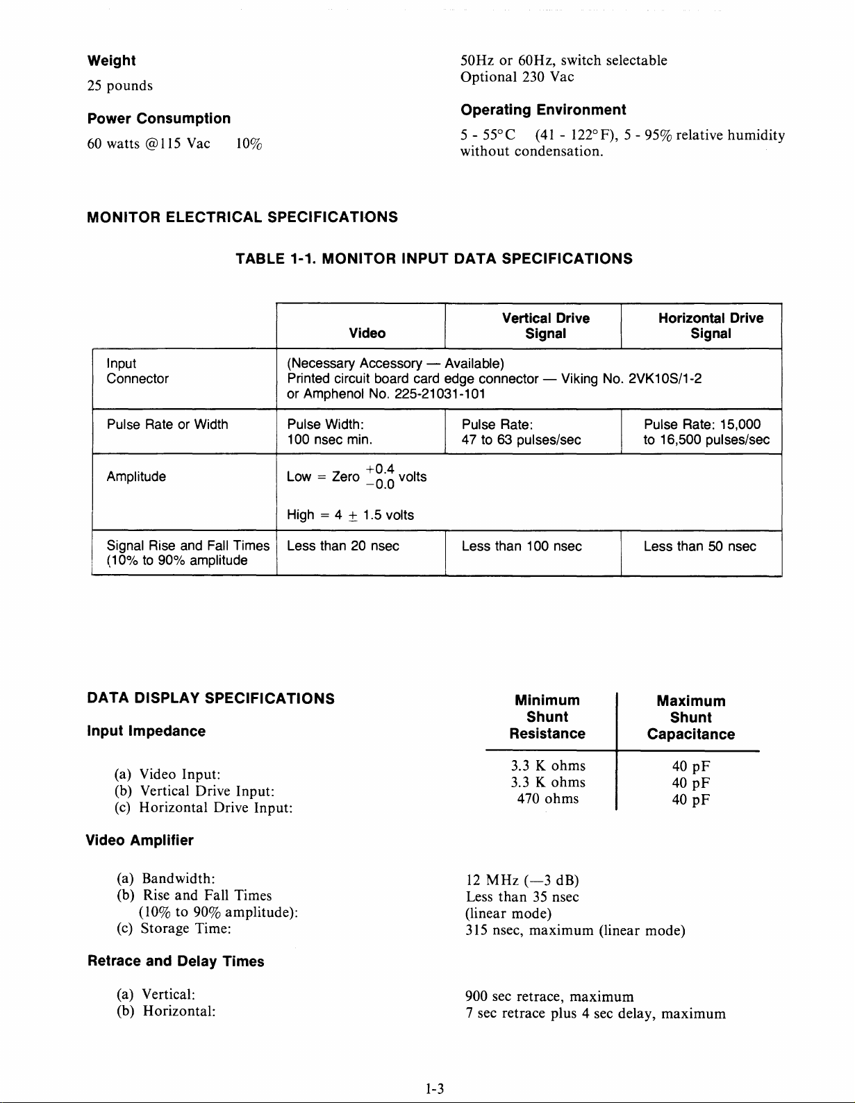
MONITOR
Input (Necessary Accessory - Available)
Connector Printed circuit board card edge connector - Viking No. 2VK10S/1-2
Pulse Rate or Width Pulse Width:
Amplitude
ELECTRICAL SPECIFICATI,ONS
10%
TABLE 1-1.
or Amphenol No, 225-21031-101
100 nsec min.
Low
MONITOR
Video
= Zero
~g:6
INPUT
volts
Operating Environment
5 - 55°C
without
DATA
Pulse Rate:
47 to 63 pulses/sec
(41
- 122°F), 5 - 95% relative humidity
condensation.
SPECIFICATIONS
Vertical
Drive
Signal Signal
Pulse Rate: 15,000
to 16,500 pulses/sec
Horizontal
Drive
Signal Rise and Fall Times
(10%
to
90% amplitude
DATA DISPLAY
Input Impedance
SPECIFICATIONS
(a) Video Input:
(b) Vertical Drive Input:
(c) Horizontal Drive Input:
Video Amplifier
(a) Bandwidth:
(b) Rise
and
Fall Times
(10% to 90% amplitude):
(c) Storage Time:
High
= 4 ± 1.5 volts
Less than 20 nsec
Less than 100 nsec
Minimum
Shunt
Resistance
3.3 K
ohms
3.3 K
ohms
470
ohms
12
MHz
(-3
dB)
than35nsec
Less
(linear mode)
315 nsec,
maximum
Less than
Maximum
Shunt
Capacitance
40
40
40
(linear mode)
pF
pF
pF
50
nsec
Retrace and Delay Times
(a) Vertical:
(b) Horizontal:
900 sec retrace,
7 sec retrace plus 4 sec delay,
1-3
maximum
maximum
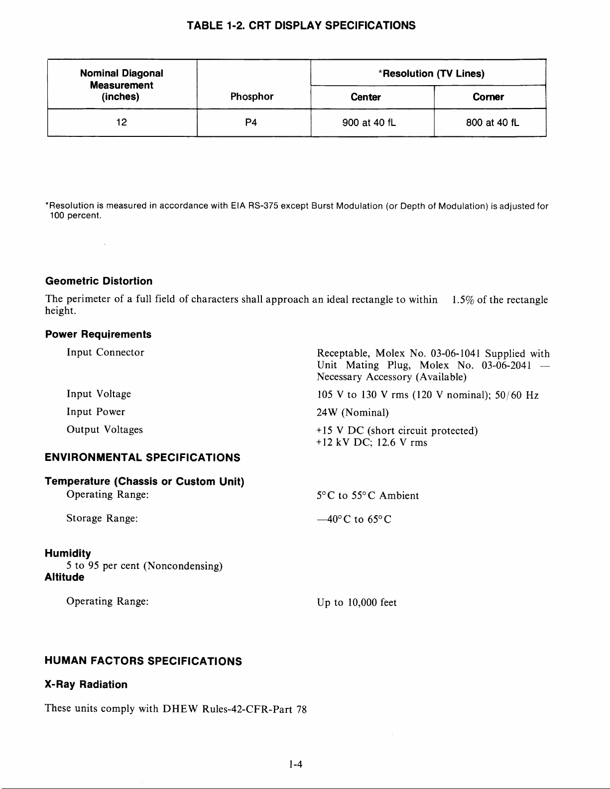
TABLE
1-2. CRT DISPLAY SPECIFICATIONS
Nominal Diagonal
Measurement
(inches) Phosphor
12
*Resolution is measured in accordance with EIA RS-375 except Burst
100 percent.
Geometric
Distortion
The perimeterofa full fieldofcharacters shall
P4
approachanideal rectangletowithin 1.5%ofthe rectangle
height.
Power
Requirements
Input
Connector
Receptable, Molex No. 03-06-1041 Supplied with
Unit Mating Plug, Molex No. 03-06-2041 Necessary Accessory (Available)
Input
Voltage
Input
Power
Output
Voltages
ENVIRONMENTAL
SPECIFICATIONS
105Vto
24W (Nominal)
+
15VDC
+
12
*Resolution (TV Lines)
Center Corner
900 at 40 fL 800 at 40 fL
Modulation
(or
DepthofModulation) is adjusted
130
V rms (120 V nominal);
50/60
(short circuit protected)
kV DC; 12.6 V rms
for
Hz
Temperature
(ChassisorCustom
Operating Range:
Storage Range:
Humidity
5to95
per cent (Noncondensing)
Altitude
Operating Range:
HUMAN
FACTORS
SPECIFICATIONS
X-Ray Radiation
These units comply with
DHEW
Unit)
Rules-42-CFR-Part
5°Cto55°C Ambient
-40°Cto
Up to 10,000 feet
78
1-4
65° C
2.1
GENERAL
SECTION 2
INSTALLATION
This section contains
the
ADM-3A
instructions
ADM-3A,
setting internal switches, connecting cables,
turning-on power.
2.2 VISUAL INSPECTION
It
is
recommeded
carton
should
Carefully inspect
damage
undergone stringent quality inspections
operational
in perfect operating condition.
If
immediately. Save the damaged shipping
as evidence for inspection by the carrier.
Only the consignee may register a claim with the
carrier for damage during shipment. However, Lear
Siegler
customer
2.3 INSTALLATION
The
of
and
you
the unit is damaged, notify the carrier
Data
ADM-3Aisdesignedtooperate in a wide range
environmental conditions:
5-55°C (41-122°F), 5-95% relative humidity
without condensation.
and
and
installing it in a suitable environment,
all packing materialstoprevent
wishtotransportorship the terminal.
during shipping. The terminal has
tests
Products
should such action be necessary.
informationtoaid in installing
preparing
information
that
yousave the originalshipping
your
priortoshipping; it left the factory
it for use. Included
for inspecting the
ADM-3A
will
cooperate
are
and
damage
for signs
container
fully with the
of
and
to
The unit is designed
any
other
suitable hard, flat surface.
In cold climates, care should be exercised
to
allow the
to
equalize with
removing the unit from the shipping
carton; this will prevent moisture from
condensing
warm
soft surface, such as carpeting, which
would obstruct the flow
through
could result in overheating
to
the unit.
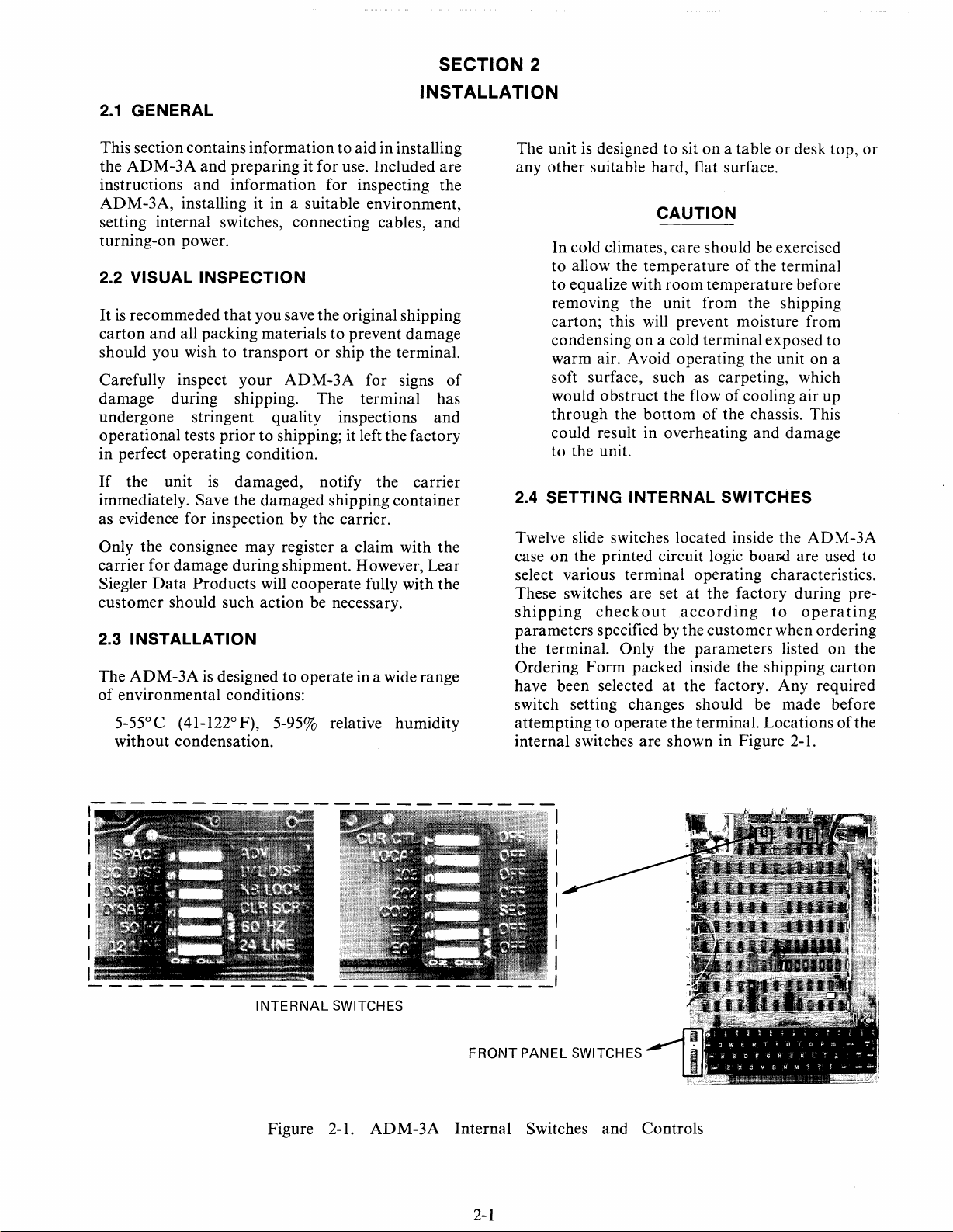
2.4 SETTING INTERNAL SWITCHES
Twelve slide switches located inside the
caseonthe printed circuit logic boar-d are used to
select various terminal operating characteristics.
These switches are set
shipping
parameters specified by the
the terminal. Only the parameters listed
Ordering
have been selected
switch setting changes should be made before
attemptingtooperate the terminal. Locationsofthe
internal switches
Form
on
air. Avoid operating the unit on a
the
checkout
packed inside the shipping
sitona tableordesk top,
CAUTION
temperatureofthe terminal
room
temperature
a cold terminalexposed
of
cooling
bottomofthe chassis. This
at
the factory
according
customer
at
the factory. Any required
are
shown in Figure 2-1.
before
air
and
damage
ADM-3A
during
to
operating
when ordering
to
up
pre-
on
carton
or
the
,----------------------
I
I
I
I
I
I I
I I
I
-
--
-- --
---------
INTERNAL
Figure 2-1.
SWITCHES
ADM-3A
-------,
FRONT
Internal
2-1
PANEL
Switches
SWITCHES
and
Controls
WARNING
Always
from
ADM-3A
disconnect
the
power
source before
case
to
the
access
ac
power
opening
any
component.
Switch functions
are
described below:
SPACE - ADV
In
SPACE
Pressing
AL
WAYS
with a space code
In
ADV
between a
the cursor ma
not
overwrite display
position, selects destructive cursor.
the
space
bar
or
receiving a space
overwrites
the
display
and
advances the cursor.
memory
position, selects non-destructive
Return
and
subsequent
1 be advanced but a space code does
y
memory
Line
locations.
codeisdestructive between a Line Feed
Return.
UC
DISP -
In
UC
DISP
characters
such
but
lower caseisnot
the
switch
In
UIL
lower case
with the
U/L
DISP
position, allows displayofupper
only.
Lower
are
convertedtoupper
case codes
case
installedorifitisnottobe utilized,
must
stay in
DrSp
position, allov/s displayofupper
characters
UpperILower
the
UC
DISP
if the
terminalisequipped
Case option.
are
cord
the
internal
code
location
cursor
Feed
only;
The
space
and
the
transmitted
for
display.
position.
next
case
as
and
On
terminals with
switch
must
CURSOR
In
the
ON
reverse
block
be settothe12LINE
CONTROL
position, this switch selects a moveable
cursor
standard
12
which accesses
line display this
position.
any
areaonthe
screen.
In
the
OFF
position, this switchselects the
double-underline
entered
Upward
occur
the
from
the
scrolling
when a full lineofdata
bottom
line in either mode.
cursor.
In
this mode,
bottomofthe screen.
and
top-of-the-page overflow
has
been entered
standard
data
from
is
LOCAL - OFF
103 - OFF
202 - OFF
These three switches
operation
for
one
interfacingtothe
are
usedtoselect
of
the following
computer:
(1)
methods
without
ADM-3A
of
modems
(direct, local connection), (2) with 103-type
If
modems,
appropriate
the
connection
must
Setting
to Send)
or
(3) with 202-type modems. The
switch is set (left position)
method
be settothe
the
LOCAL
to
rise
OFF
used; the
positions.
other
switch causes line
and
fall with each
according
two switches
C.A
ll
(Request
character
to
transmitted.
DISABLE -
In
DISABLE
KB
LOCK
position, prevents locking
keyboard.
In
KB
LOCK
position, allows
electrically disabled (locked) by
codes.
DISABLE - CLEAR SCREEN
In
DISABLE
displayed
position, prevents clearing
information
except
repetitive line feeds.
In
CLEAR
clear
code
(CTRL
SCREEN
ADM-3A
screen by
Z).
position, allows
transmittingacontrol
50Hz - 60 Hz
Selects
set
50Hzor60Hz
to
correspond
display refresh rate;
with
input
power
12 LINE - 24 LINE
If
terminalisequipped
this switch
may
with 24-line display
be used
to
seiect i2
display.
keyboard
remote
by
executing
computer
frequency.
or
to
control
must
option,
24
iine
be
to
be
of
of
Setting the
Setting the 202 switch enables 202-type
using the
change
channel
With all three switches off,
103
switch holds
secondary
the
directionofdata
channelorturnaround
over the
(half-duplex operation).
CAisheld low all the
CA
high,ifrequired.
primary
operation
code
to
data
time.
CODE
- SEC CHAN
This switch is active only with the 202 switch
(described above) in the
select the
operation
In
SEC
using
is
summarizedinthe
The
by a
data
EXTorEaT,
methodofline
with 202-type modems.
CHAN
the
secondary
CODE
turnaround
channel.
position, enables line
position
code
The
as selected by the switches described
on
turnaround
channel. 202
backofthis
allows line
transmitted
turnaround
position.Itis
for
half-duplex
turn-around
modem
handbook.
turnaround
over
the
code
may
used
operation
control
primary
be either
to
below.
I""v-r
I:.J\
I-vrr
,...~~
EOT-OFF
2-2
One
of
these two switchesissettothe
position
to
select the line
primary channel
(See
CODE-SEC
202
and
CODE
beonand
selected, oneofthese switches
the
other
selected,or202 off,
must be set to the
operation
CHAN
off; with 202
both
the
OFF
positions.
turnaround
with 202-type modems.
switch description.) With
and
ETX
and
SEC
EOT
on
(left)
code for
must
CHAN
switches
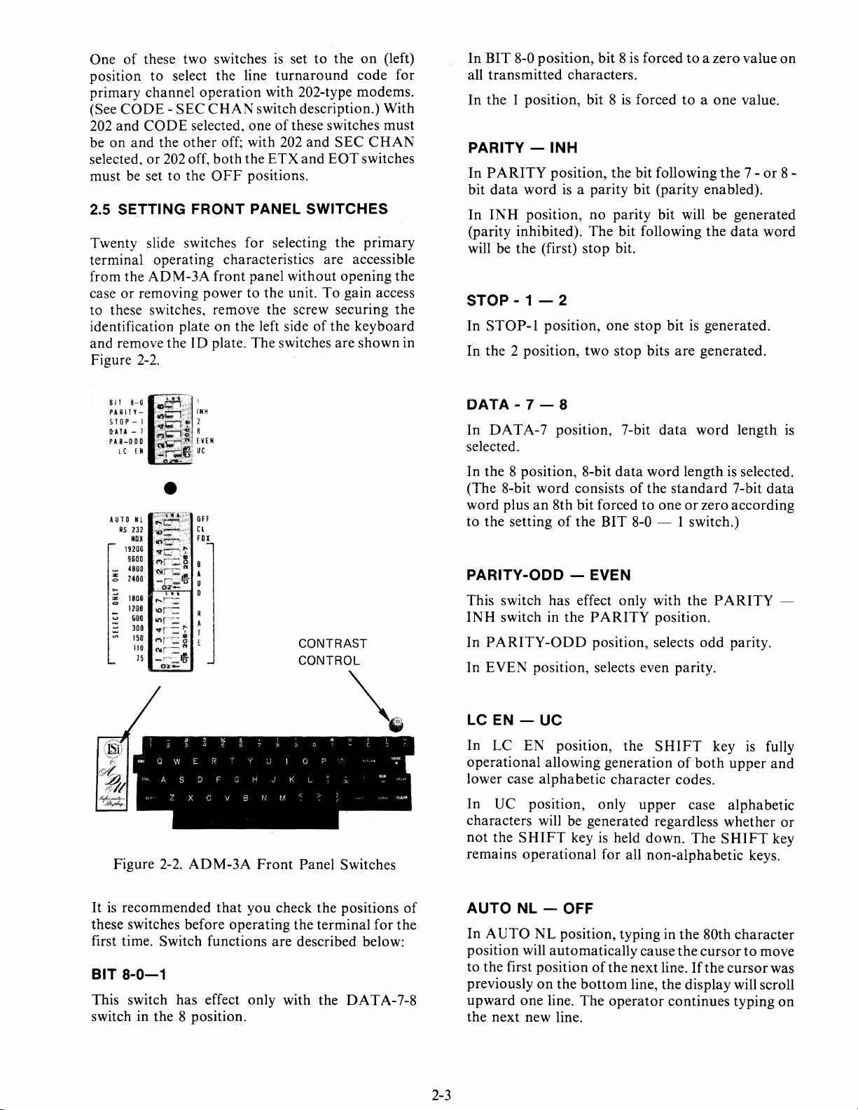
2.5 SETTING FRONT PANEL SWITCHES
Twenty slide switches for selecting the
primary
terminal operating characteristics are accessible
from the
case
ADM-3A
or
removing power to the unit.Togain access
front
panel without opening the
to these switches, remove the screw securing the
identification plate
and remove the10plate. The switches are
on
the left sideofthe
keyboard
shown
in
Figure 2-2.
In
BIT
8-0 position, bit 8isforcedtoa zero value
all
transmitted
In
the I position, bit 8isforcedtoa
PARITY
In
PARITY
bit
data
wordisa
In
INH
(parity inhibited).
will be
the
characters.
-INH
position,
position,
(first)
the
bit following
parity
no
The
stop
bit (parity enabled).
parity bit will be generated
bit following
bit.
STOP - 1 - 2
In
STOP-I
In the 2 position,
position, one
two
stop
stop
bits
one
value.
the
7 -or8 -
the
data
bitisgenerated.
are
generated.
on
word
BIT 8-0
PARITVSTOP
I'lATA
- J
PAR-ODD
l C £
AUTO
RS
1I0X
19200
9600
4BOO
:;
2400
...
:;
18011
1200
..,
....
I
Figure 2-2.
- I
II
•
III Off
232
600
300
ISO
ilO
15
It
3
Q
W
A
S
Z
X
ADM-3A
I
IHH
2
e
[
VEil
UC
Cl
fOX
E R
D
C
DATA - 7 - 8
In
OAT
A-7 position, 7-bit
data
word
length
is
selected.
data
word
In the 8 position, 8-bit
(The 8-bit
word
consistsofthe
lengthisselected.
standard
7-bit
data
word plusan8th bit forcedtooneorzero according
to the setting
of
the
BIT
8-0 - I switch.)
PARITY-ODD - EVEN
This switch has effect only with
INH
switch in the
PARITY-ODD
CONTRAST
CONTROL
~
!,
y
F
G
V
N
M
8
p
0
K
"
In
In
EVEN
LC EN -
position, selects even parity.
UC
In LC EN position, the
operational
lower case
allowing
alphabetic
In UC position, only
PARITY
position, selects
generationofboth
character
upper
characters will be generated regardless
not
the
Front
Panel Switches
remains
SHIFT
operational
keyisheld down.
for all
the
PARITY
position.
odd
parity.
SHIFT
key
upper
codes.
case alphabetic
whether
The
SHIFT
non-alphabetic
is
keys.
-
fully
and
or
key
It
is
recommended
these switches before
first time. Switch functions
BIT
8-0-1
that
you check the positions
operating
the terminal
are
described below:
This switch has effect only with the
switch in the 8 position.
OAT
for
A-7-8
of
the
AUTO
In
AUTO
position will
to the first position
previously
upward
the
next
2-3
NL - OFF
NL
position, typing in
automatically
on
the
bottom
one line.
The
new line.
the
80th
cause the
of
the next line.Ifthe
cursortomove
line, the display will scroll
operator
continues typing
character
cursor
was
on
In
OFF
position, the
is
disabled. Continued typingatthe 80th character
position transmits each new character
the 80th character
RS232 - CL
In
RS-232 position, selects RS-232C communi-
at
cations
connector
In
CL
the
on
the rear panel.
position, selects 20m A current loop
communications
automatic
on
the display.
MODEM
at
the
New Line function
and
changes
(computer) interface
MODEM
interface
connector.
HDX-FOX
In
HDX
Characters typed are transmitted and automatically
echoed back from the
display.
position, selects half duplex operation.
ADM-3A
110 Channel for
top
of
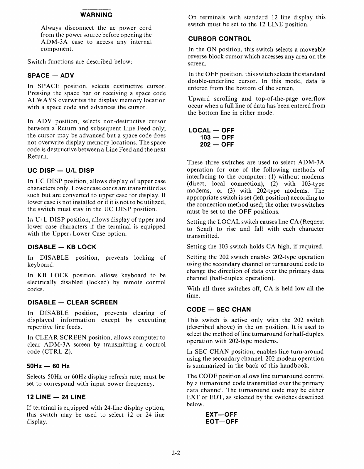
the case. (See Figure 2-1.) Background
intensity
terminal
is
is
readjustment
adjusted
at
the factory before the
shipped and should
priortousing the terminal.
not
require
In
FDX
position, selects full duplex operation.
Characters typed are displayed only if echoed back
by the
computerormodem.
Communication Rate Switches
19200
9600
B These switches are used to select
4800
A the
U
2400
1800
O puter and auxiliary device.
send/receive
communications
rate for
with the com-
data
1200
600
R Setting one switch to
A hand (BAUD RATE)
300
150
T selects the associated rate.
the left-
position
110
EI
75
NOTE
Only one
selected (left position)
2.6 SETTING DISPLAY
BAUD
RATE
switch may be
at
a time.
CONTROLS
Figure 2-3. Background Intensity
Because
(located in
the
topofcase)
WARNING
Background
control must be adjusted with the
3A case open with power on, it should be
adjusted only by qualified service
personnel.
ON/OFF
The power
Switch
ONIOFF
switchislocatedonthe
3A rear panel.
2.7
CONNECTING
ON POWER
a.
With the
position, plug the
proper
the
CABLES AND
ONIOFF
ADM-3A
AC
power outlet.
switch in the
Control
Intensity
ADM-
ADM-
TURNING
OFF
power cord into
Contrast
The
Contrast
keyboard
operatortoadjust brightnessofthe characters
the
optimum
for
turned
clockwisetoincrease character brightness,
counterclockwise
Background intensity
controlislocatedtothe rightofthe
on
the
ADM-3A
readability. The
to
front panel.Itis
Contrast
decrease brightness.
used by
knob
A Background Intensity potentiometerislocated
inside the
ADM-3A
caseonthe circuit
board
in the
b. Connect the interface cable from the
or
modem
connector
c.
Connect the interface cable from the auxiliary
is
device (if present in your system)
EXTENSION
ADM-3A
d. Check the settings
verify
that
operation in
to
the
on
the
ADM-3A
interface connector
rear panel.
of
all front panel switches
the
terminalisset
your
system. Ivlakt; switl;h setting
MODEM
rear panel.
up
for
computer
interface
to
the
on
the
to
proper
changes if necessary.
2-4
e.
Set the ON /
position.
f.
Allow approximately20seconds for the unit
warm up.
OFF
power switch to the
• If the cursor control mode has been
selected, a reverse block cursor should
appear
• If the cursoe control mode
underline cursor should
bottom
• If the cursor does
contrast control
proper
in the
upper
left cornerofthe screen.
leftofthe screen.
not
on
intensity.
is
appear
appear, adjust the
the front panel for
OFF
near
ON
to
an
the
NOTE
If the Full-Duplex mode
at
typing
characters unless echo-back
by the
duplex
only if clear-to-send
disconnected.
the keyboard will not display
computer
is
selected,
or
modem. If half-
data
will be displayed
is
presentorcable
is
selected,
is
provided
is
2-5

3.1
GENERAL
SECTION 3
OPERATION
This section contains information
for using the
ADM-3A
keyboard facilities, and for
programming control functions
The keyboard allows the
transmit to the
128
all
3.2 DISPLAYING CHARACTERS
In the
USASCII character codes.
standard
computer
operator
(and/orauxiliary device)
ADM-3A,
and
instructions
at
the computer.
to generate and
64
characters are
displayed on the screen (upper case alphabet,
numbers
most symbols
and
punctuation).
and
When a non-displayable lower case character
typed, the
proper
lower case codeistransmitted
but
the characterisdisplayed as upper case.
If
your terminal contains the
95
Display feature,
characters will be displayed
(upper and lower case alphabet, numbers
and
punctuation
symbols).
NOTE
Upper/Lower
and
Case
all
Typingatthe keyboard always generates
codes which are transmitted; however, in
to
order for characters
be displayed
control codes to affect the
display the codes must be echoed back
the
ADM-3A
display memory
control logic, either by the
(FDX)
or
the
ADM-3A
I/O
and
ADM-3A
to
and
computer
Channel
(HDX).
All display actions described in the key
that
descriptions
follow assume the
generated codes are echoed.
If
the front panel
AD
V position, the space codeisnon-destructive
after typing the
or
computer
can space over
SPACE-ADV
RETURN
switchisin the
key;
that
is, the
operator
dataonthe line without
overwriting each character with a space. The space
bar
remains non-destructive following a
function until a LINE
LINE FEED Key
FEED
codeisgenerated.
RETURN
A codeisgenerated by this key which causes the
to
cursor
on
upward one line.
is
cursor to the first character position
SHIFT Keys
Eitherofthe two
typing
alphabetic characters
shown in the upper portion
move downward one line.Ifthecursorwas
the
bottom
line, the entire display will scroll
LINE
FEED
does
not
of
SHIFT
another
Setting the
key to generate
"LC
the front panel
keysisheld down while
or
to generate the character
of
a typed key.
NOTE
EN - UC" switch
ID
plate
to
return the
the new line.
upper
case
under
the UC
position causes upper case alphabetic
characters
without the
SHIFT
key remains operational for all
be generated with
SHIFT
key depressed. The
or
to
non-alphabetic keys.
RUB (Rubout) Key
When typed while holding down the
transmits a non-displayable
Rubout
SHIFT
key
code (ASCII
DEL)tothe computer. The cursorisnot advanced
and
the character code stored in the
ADM-3A
display memoryisnot overwritten.
3.3 SPECIAL
FUNCTION
KEYS
In additiontothe displayable character keys, the
ADM-3A
keys for various terminal
functions. Use
RETURN Key
keyboard contains a
and
of
these keysisdescribed below;
number
of
system control
other
A codeisgenerated by this key which moves the
of
cursor to the first character position
the line.
The
Rubout
computer
functionisnormally usedtotell the
that
a previous character should be
deleted.
The lower case RUB key transmits/displays
underline.
REPT (Repeat) Key
When held down while pressing a character key,
at
repeats the character
the terminalisoperatingata
a rateof12.5 per second.
baud
rate
permit 12.5 cps transmission, the repeat rate
reducedtothe transmission rate.)
3-1
that
will
an
(If
not
is
Space Bar
The
Space
key.
Causes
and
blank
exceptions
Bar
is'
consideredadisplayable
the
ASCII
storedinthe
spacetoappearonthe
see
code
ADM-3A
RETURN
CTRL (Control) Key
When
held
down
while
the
code
patternofthe
to
oneofthe
Code
chart.
The
ADM-3A
possible
haveafunction
in
Table
two
ASCII
3-1.
control
is
capable
codes,
within
foraspacetobe
display
screen.
Key).
typing
typed
the
another
key.
code
columnsinthe
of
although
machine.
The
generating
only
character
transmitted
memory
(For
key,
codeisforced
These
the
modifies
14
of
are
and
ASCII
all 32
only
them
listed
column-code
sequence.Inany
codetobe
CLEAR
a
Typing
SHIFT
function
SCREEN
(SPACE
mde,
transmittedtothe
Key
the
CLEAR
key clears
may
-
the
be
disabledbythe
DISABLE
through0)to
causes
key while
entire
the
computer.
screentospaces. (This
Switch.)
complete
ASClI
holding
internal
ESCape
down
CLEAR
the
the
HERE IS Key
If
your
terminalisequipped
Answer
identification
special
the
In
capability,
Back
memory)toidentify
computer
terminals \\lithout
this key
feature,
message
that
typing
(storedinthe
a message istofollow.
hasnofunction.
with
this key
your
terminal
iA,-utomatic
the
Automatic
transmits
ADM-3A
and
alert
i~ns,ver
Back
an
in a
Backspace (CTRL/H).
typed
while
holding
moves
the
transmittedtothe
in
Bell
ADM-3A
non-destructively
left.
The
conjunction
(CTRL/G)
and
CTRL/
computer.
with
Sounds
transmits
down
the
Each
time
theHkey
the
CTRL
one
character
H
backspace
CTRL/Hmaybeused
Repeat
the
the
CTRL/
key.
audible
key,
position
beepinthe
G bell
the
UPLINE (CTRL/K)
When
reverse-block
Return (CTRL/M).
RETURN
Line Feed (CTRL/J).
the
in
LINE
the
Cursor
cursortomove
key.
FEED
key.
Control
Duplicates
Duplicates
Mode,
upward
the
functionofthe
the
causes
one
function
Lock Keyboard (CTRL/O). Electrically
(disables)
further
unlocked
clearing
power
FORWARD SPACE
When
reverse
HOME
When
reverse
cornerofthe
the
ADM-3A
keyboard
byacontrol
the
off,
thenonagain.
in
the
block
activities.
screen
with
Cursor
cursortoadvance.
CURSOR (RS)
in
the
Cursor
block
cursor
screen.
keyboard,
The
code
from
the
CLR
(CTRL/M)
Control
Control
to
return
preventing
keyboard
the
keyorby
Mode,
Mode,
to
the
computer,
causes
causes
upper
ESCAPE KEY (ESC)
When
cursor
character,arow
in
Cursor
sequence.
Control
ESC
code
(SPACE
must
Mode,
be
followed
through7)and
initiatesaload-
cursor
code
code.
line.
locks
can
turning
by
an
to
the
of
any
be
the
the
left
is
is
BREAK
This key
function,
message.
Key
activates
normally
the
standard
usedtointerrupt
teletypewriter
an
incoming
Break
NOTE
The
Break
the
the
cause
your
BREAK
key
down
the
terminal.
functionissustainedaslong
keyisheld
foranextended
computer
down.
to
disconnect
period
as
Holding
may
from
3.4 PROGRAMMING & WORD STRUCTURE
The
=
a
computertowhich
has
full
control
functions
keyboard,
be
executed
The
ting
character
codes
3.4.1
The
control
Backspace
non-destructively
left.
which
plus a few
computer
the
appropriate
codes
will be
are
from
controls
will be
recognized
Remote Control Functions
remote
computer
functions:
BS
Bell BEL (CTRL/G).
the
ADM-3A.
Return CR (CTRL/M)
destruciively
present
to
line.
the
over
the
possible
additional
the
computer.
the
ASCII
displayed,
and
can
(CTRL/H).
one
character
Sounds
the
first
ADr-.1-3,A.isinterfaced
terminal.
from
functions,
ADM-3A
codes.
acted
perform
Moves
the
Moves
character
All
control
the
ADM-3A
can
by
transmit-
Displayable
and
valid
control
upon.
the
following
the
cursor
positiontothe
audible
the
positionofthe
beep
cursor
also
in
non-
3-2
Line Feed
IF
(CTRl/J).
Causes the entire
display to move upward one line, leaving the
cursor positioned in the same
character
position
on the next new line.
Upline (VT) - Moves cursor up vertically when
Cursor
in
Forward Space (FF) - Moves
when in
lock
locks the
Control Mode.
Cursor
Control
Keyboard
ADM-3A
cursor
Mode.
SI
(CTRl/O).
Electrically
keyboard, disabling all
forward
keyboard functions.
Unlock Keyboard SO
ADM-3A
keyboard, restoring all keyboard
(CTRl/N).
Unlocks the
functions.
Clear Screen SUB
character
memory
(This function
positions in the
and
clears the screentoblank
may
(DISABLE-CLEAR
Home Cursor (HOME) - Causes the
returntothe
in the
load
Cursor (ESC =YX) - This
Cursor
upper
Control
sequence causes the
row
and
and
X respectively.
column
defined bythe
The Reference Tables
(CTRl/Z).
ADM-3A
Clears all
display
spaces.
be disabled by
SCREEN
the
internal
switch.)
cursor
left
cornerofthe screen, when
Mode.
four-character
cursortobe positionedtothe
3-1
and
ASCII
3-2ofthis
values
manual
of
to
show the actual binary codes generated by the
ADM-3A
and
used for
computer
controlofthe
terminal.
Y
Table 3-1.
ASCII
Code Mnemonic Function ADM-3A
CTRL/@
CTRL/A
CTRL/B
CTRL/C
CTRL/D
CTRL/E ENQ
CTRL/F
CTRL/G BEL
CTRL/H BS
CTRL/I HT
CTRL/J
CTRL/K
CTRL/L
CTRL/M
CTRL/N
CTRL/O
CTRL/P
CTRL/Q
CTRL/R
CTRL/S
CTRL/T
CTRL/V
CTRL/V
CTRL/W
CTRL/X
CTRL/Y
CTRL/Z
CTRL/[
CTRL/x
CTRL/]
CTRL/A
NUL
SOH
STX
ETX
EaT
ACK
LF
VT
FF
CR
SO
SI
OLE
OC1
OC2
OC3
DC4
NAK
SYN
ETB
CAN
EM
SUB
ESC
FS
GS
RS
AD
M-3A Control Codes
as
Available
modem operation
Availableassecondary channel line
modem operation
Initiates
option*
Sounds audible beep in
Backspace
Line Feed
Upline
Forward Space
Return
Unlock
Lock
Keyboard*
Clear Screen
Initiate Load Cursor
Home
secondary channel line
10 message in
Keyboard*
Cursor
terminals
AOM-3A
with
turnaround
turnaround
automatic
code
for
code
for
"Answer
202
202
Back"
*Executable
only
from
computer.
3-3
Table 3-2 USASCII Character Codes
GRAPHIC CHARACTER
CONTROL SET
BITS BITS
4321
765
0000
0001
0010
0011
0100
0101
0110
0111
1000
1001
1010
1011
......
f"\f"\
IIUU
0
000
NUL
SOH
STX
ETX
EOT
ENQ
ACK
BEEP
BS
HT
LF
VT
........
rr
1
001
OLE
DC1
DC2
DC3
DC4
NAK
SYN
ETB
CAN
EM
SUB
ESC
....
t'"'
rv
2
010
SP
!
"
# 3
$
0/0
&
( 8
) 9
*
+
,
3
011
1 A
2 B
4
100
@
5 6
101
P
Q
R
C S
4 0 T d
5 E
6
7 G W
F V
U
H X
Y i
Z j
[
\
,/
...........
I
J
K
I \ I
L
110
a
b
c s
e
f v
9
h x
k
I
7
111
P
q
r
t
u
w
Y
z
{
1101
1110
1111
""
CR
SO
SI
GS
RS
US
.........
Control
Codes
(Generated by
holding
key
the
key shown in
CTRL
while
typing
corresponding
col-
umns 4 and 5.)
3.4.2 Data Character Format
The
ADM-3A
America
change).
many
ADM-3A
the
f_l
..
n
_n_;"'u
\PiU",
peu
USASCIIisa 7-bit code. But because
of
the computers
iLy
uses
Standard
USASCII
Code for Information Inter-
and
(United States
other
devices to which
may be interfaced use 8-bit words
"'_
.,,;
...
\.."'
.....
Vi"'lLUVUL
_n_;"'u\
peu
"'\"0
iLyhLa,,-
i\
nl\.,f'2i\
rl.L'
",++0_"
U.L
-.)rl.
Vii"-i"
a wide choiceofword formats selectable by the user.
of
,,,
-
=
>
/
? 0
Displayable in
standard
~
M
N
ADM-3A
]
f\
+
m
}
,......
n
DEL
0
,
...
T
I
Displayable
with
ADM-3A
Upper/Lower
Case Display
feature.
3-4
The
data
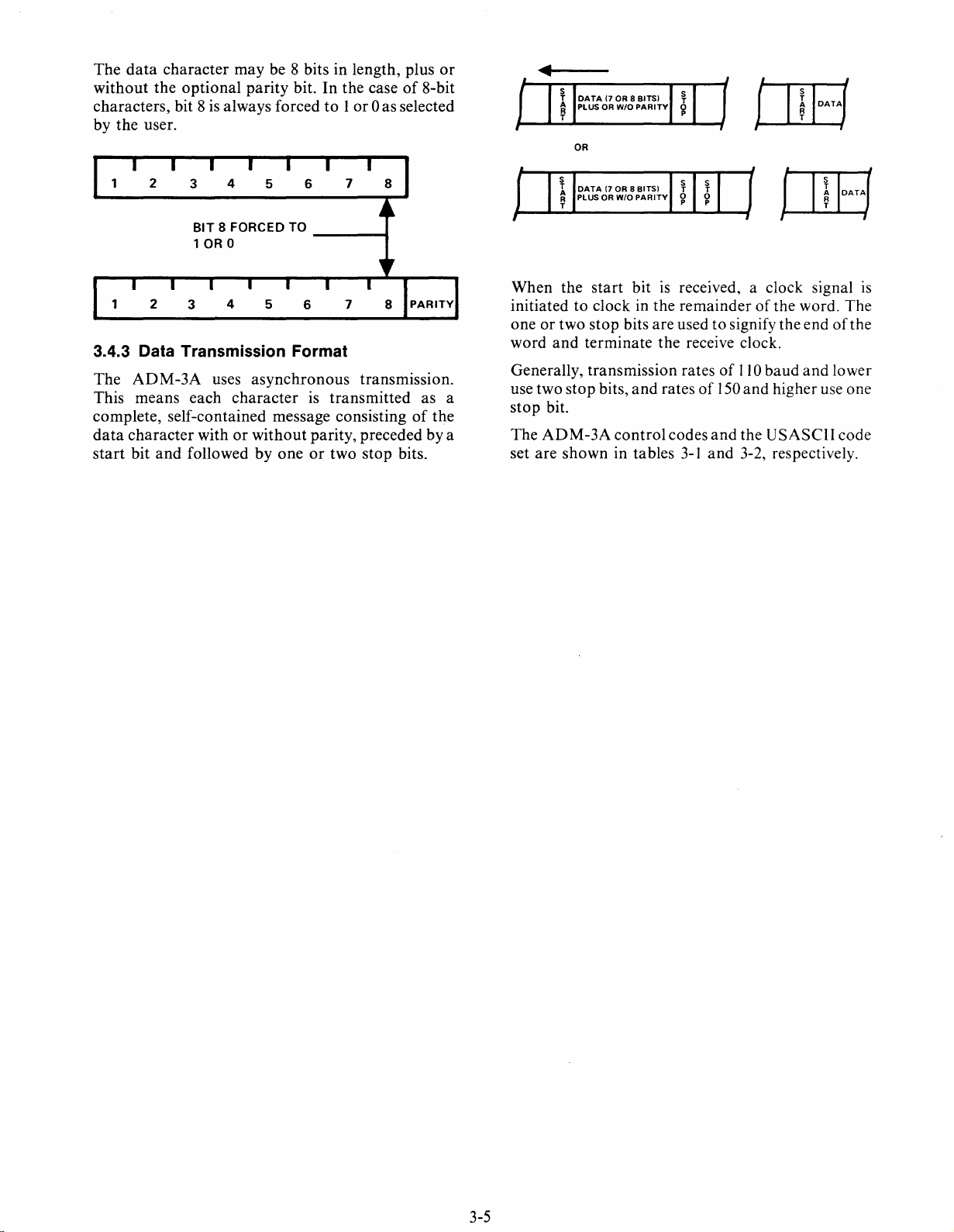
character may be 8 bits in length, plus
without
the optional parity bit.Inthe caseof8-bit
characters, bit 8
by the user.
is
always forcedto1or0as selected
or
DATA
(7 OR 8 BITS)
PLUS
OR
WIO
PARITY
OR
DATA(7OR8BITS)
PLUS OR
WIO
PARITY
3.4.3 Data Transmission Format
The
ADM-3A
This means each
uses
asynchronous
transmission.
characteristransmitted as a
complete, self-contained message consisting
data
character withorwithout
start
bit
and
followed by
parity, preceded by a
oneortwo stop bits.
of
the
When the
start
bitisreceived, a clock signal
initiatedtoclock in the remainderofthe word. The
one
or
two stop bits are usedtosignify the endofthe
word
and
terminate the receive clock.
Generally, transmission rates
use two stop bits,
stop
bit.
The
ADM-3A
and
control
ratesof150
codes
set are shown in tables
3-1
of
110
baud
and
higher use one
and
the USASCII code
and
3-2, respectively.
and
lower
is
3-5

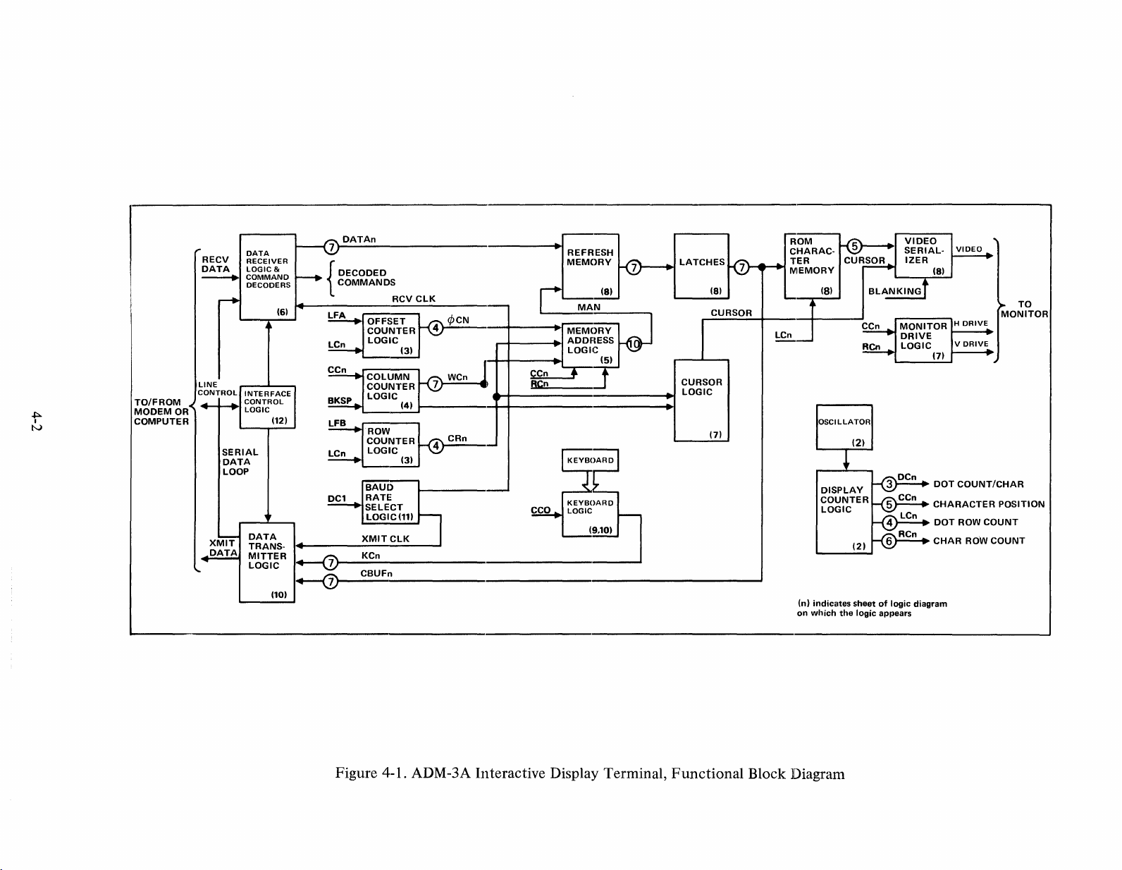
4.1
GENERAL
SECTION
4
THEORY OF OPERATION
4.2.2 Display Refresh Operation
This section describes the
ADM-3A
first described with reference to
diagram, and then each element shown in the block
diagram
illustrations and to logic diagrams contained in
Section 6
4.2 GENERAL
The general organizationoflogic in
shown in figure 4-1. This figure divides
logic into functional blocks and shows the
relationships between blocks.
sheet
block
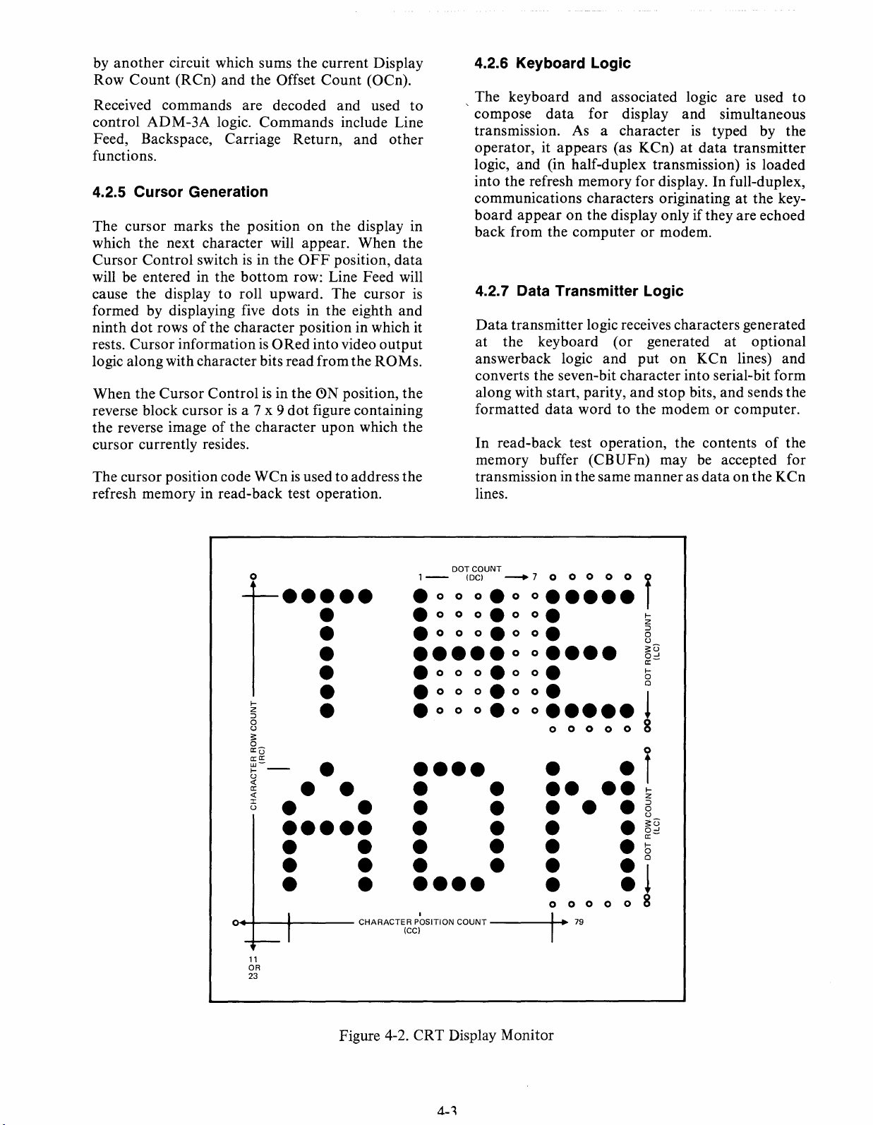
4.2.1 Display Generation
Signals
maintained
counters (display counter logic).
The first counter (the
pulses from
timing signal in the ADM-3A. The purpose
dot
sequential address
the presettingofthe video serializer. Each increment
of
the counter defines the positionofa single
any line (dot row)
Any character
(figure 4-2). A character position
and nine dots high
characters
A single horizontal sweep
produces all dots in a given
characters in the character row. The character
counterisincrementedfor every seventh dot column
to define the position
At the end
incremented
The character row counter
ninth dot line to define the position
character row.
The four display counter outputs control memory
addressing, character generation, and many
functionsofADM-3A
performs its different functions. Logic
is
described with reference to specific
of
this manual (Drawings).
FUNCTIONAL
of
the logic diagram
is
detailed.
that
cause a display to be generated and
on
the screen arefurnished by a string
an
oscillator. This clockisthe primary
counteristo
both
of
and
time the presentation
to
of
any character in the display.
is
made upofa 5 x 7
to
provide 2-dot spacing between
horizontally and vertically.
of
each
dot
the next
manner
It
on
dot
counter)isclocked by
the character generator
of
each character in the row.
row, the line
dot
rowisscanned out.
is
incremented by every
logic.
in which the
an
overall block
DESCRIPTION
ADM-3A
AD
also indicates the
which logic in any
of
arrayofdots
is
seven dots wide
the
CRT
dot
row for all
counter
of
the next
M-3A
of
the
the
and
dot
beam
dot
other
of
in
is
Except when received
is
is
contents
data) are continuously presented
Memory address logic requires only sequential
character
out
Each character read from the refresh memory
stored for presentation to the
memory (and
test operation).
The
USASCII-coded character and produces a five-bit
output
row.
for each
The count
row.
4.2.3 Monitor Video and Drive Circuits
The 5-bit
character generatorispresented to the
video circuits as a serial
except during
position
sweep drive signals, with horizontal drive triggered
by the
triggered when the character row
(standard)or24 (optional).
4.2.4 Receiving and Storing Data
Data
3A
line. Baud rates are derived from the LSB
count,
clock may be the same
rate option).
Received
which
memory address, during loading,
summing the
which represents the true position
the screen,
represents the
display has scrolled. The virtual address which
thus derived corresponds to the refresh address for
that
of
the refresh memory (an entire "page"
and
row counts (CCn and RCn)toread
the memory contentstothe storage latches.
to
data
ROM
to
data
character generation decodes the stored
specifying dotstobe displayed for each
That
is, the characterispresentedtothe
dot
row as the character rowisgenerated.
CCn
selects the
dot
row
CRT
and
row counts are usedtogenerate
startofeach
transmission rates are selected in the
match those devices on the other endofthe
DC1.The receive clock and the transmit
dataisclocked into the refresh memory,
is
addressed by memory address logic. The
Cursor
and
the Offset
numberoflines (since Reset)
row. The Refresh Addressisdetermined
dataisbeing loaded, the
of
on
the screen.
ROM
transmitterlogicfor read-back
dot
pattern
data
read from the
data
stream, continuous
retrace periods.
dot
row,
and
count
or
different rates (split
Row Position
of
Count
character
dot
ROMs
for each
Character
vertical drive
reaches
is
formed by
Count
the cursor
(OCn), which
ROM
monitor
CRT
AD
of
the
baud
(CRn)
that
dot
M-
dot
on
the
12
is
is
4-1
+:>.
I
tv
TO/FROM
MODEM
OR
COMPUTER
RECV
DATA
LINE
CONTROL
SERIAL
DATA
lOOP
DATA
RECEIVER
LOGIC
&
COMMAND
DECODERS
INTERFACE
CONTROL
LOGIC
(12)
DATA
TRANSMITTER
lOGIC
(10)
DATAn
DECODED
COMMANDS
{
(6)
~
----0-~-----.-----.----'
+---0)--------------.--------1
KCn
CBUFn
RCV
ClK
....-.....-----+-1
REFRESH
MEMORY
MEMORY
ADDFIESS
lOGIC
(5)
(9.10)
lATCHES
(8)
CURSOR
lOGIC
(7)
(n)
on
indicates
which
OSCILLATOR
sheetoflogic
the
logic
appears
DOT
CHARACTER
DOT
CHAR
diagram
VIDEO
COUNT/CHAR
POSITION
ROW
COUNT
ROW
COUNT
Figure 4-1. ADM-3A Interactive Display Terminal,
Functional
Block Diagram
by
another
Row
Received commands are decoded and used
control
Feed, Backspace, Carriage Return,
functions.
4.2.5 Cursor Generation
The cursor marks the position
which the next character will appear. When the
Cursor
will be entered in the
cause the display to roll upward. The cursor
formed by displaying five dots in the eighth
ninth
rests.
logic alongwith character bits read from the ROMs.
When the
reverse block cursor
the reverse image
cursor currently resides.
The cursor position code WCn
refresh memory in read-back test operation.
circuit which sums the current Display
Count
dot
Cursor
(RCn) and the Offset
ADM-3A
Control
rowsofthe character position in which it
Cursor
logic.
Commands
switchisin the
bottom
informationisORed
Controlisin the
is
a 7 x 9
of
the character
Count
include Line
on
the display in
OFF
position,
row: Line Feed will
into video
0N
position, the
dot
figure containing
upon
is
used to address the
(OCn).
and
other
data
and
output
which the
to
4.2.6 Keyboard Logic
, The keyboard
compose
transmission. As a character
operator, it appears (as KCn)
logic, and (in half-duplex transmission)
into the refresh memory for display. In full-duplex,
communications characters originating
board
back from the
is
formatted
appearonthe display only if they are echoed
4.2.7 Data Transmitter Logic
Data
transmitter10gic receives characters generated
at
the keyboard
answerback logic
converts the seven-bit character into serial-bit form
along with start, parity,
In read-back test operation, the contents
memory buffer (CBUFn) may be accepted for
transmission in the same
lines.
and
associated logic are used
data
data
for
display
computerormodem.
(or
and
put
and
wordtothe modemorcomputer.
mannerasdata
and
simultaneous
is
typed by the
at
data
generated
on
KCn
stop bits, and sends the
transmitter
is
loaded
at
the key-
at
optional
lines) and
of
onthe KCn
to
the
DOT
COUNT
o 0
o 0
o 0
o 0
(DC)
0.0
0.00.
0.00.
0.00
COUNT
•
•
•
•
•
~7
00
o 0 0 0 0
0
•••••
O.
••••
•••••
000
•
••
•
•
•
•
•
•
o 0 0
r79
o 0
•
••
•
•
•
•
•
o 0
f
I-
Z
::J
0
U
:i:u
o...J
cr-
I-
0
0
!
8
f
I-
z
::J
0
U
:i:u
O...J
cr-
I-
0
0
~
0
-
~
.....
•
•
1-
•
.000.0
.000.00.
•••••
•
l-
z
::J
0
u
:i:
0
cr
crcr
w-
I-
U
«
cr
«
:I:
U
u
•
• •
•
•
•
•
•••••
•
•
•
• •
• •
•
_I
11
OR
23
I
-
-
CHARACTER
•
•
••••
•
•
•
•
•
••••
I
POSITION
(CC)
Figure 4-2. CRT Display Monitor
4.2.8 Interface Control Logic
This logic
Send
the
reverse-channel
control
the
other.
Switches
common
under
4.2.9
The
3A
is a
commercial
quality
The
construction
circuitsofthe
4.3
The
logic
diagram,
performing
Refertoblock
controls
exchanges
ADM-3A.
Clear-to-Send
between
Either
system
from
one
endofthe
internal
CRT
CRT
adapt
type
display
solid-state
the
logic
103
or
202
control.
Display Monitor
monitor
unit
installations
video
reproduction
monitor
LOGIC
following
features
for
reliability
TV
monitor
DESCRIPTION
paragraphs
representedbyeach
figure 4-1, as well as logic
functions
and
not
timing
modemorcomputer
a
code-turnaround
may
communication
to
modems,orto
employedinthe
for
useinindustrial
where
are
printed
and
are
describe
blockinthe
indicatedinFigure
diagrams
and
Request-to-
be
used
to
interface
reliability
and
desired.
circuit
uniformity.
transistorized.
the
operation
overall
and
that
accompany
or
transfer
line
with
operate
ADM-
high-
board
block
circuits
and
to
the
and
All
of
4- i.
the
text,
as well astothe
Section6in
this
manual.
logic
diagram
included
in
4.3.1 General Clear Circuit
a
Circuits
all
when
shownonsheet7of
control
logicinthe
applied
power
ADM-3A
causes
the
logic
tobeinitialized
the
+5Vdcsupply
diagram
cause
to
rise.
As
the
supply
retriggerable
signal
logic
the
CLEAR,
through
signal
actionofthe
voltage
one-shot,
the
whichisdistributed
six
inverters.Incircuit
TESTER
INITIALIZE
one-shot.
reaches
one-shot
trigger
creates
board
simulates
level
to
ADM-3A
of
the
reset
testing,
a
the
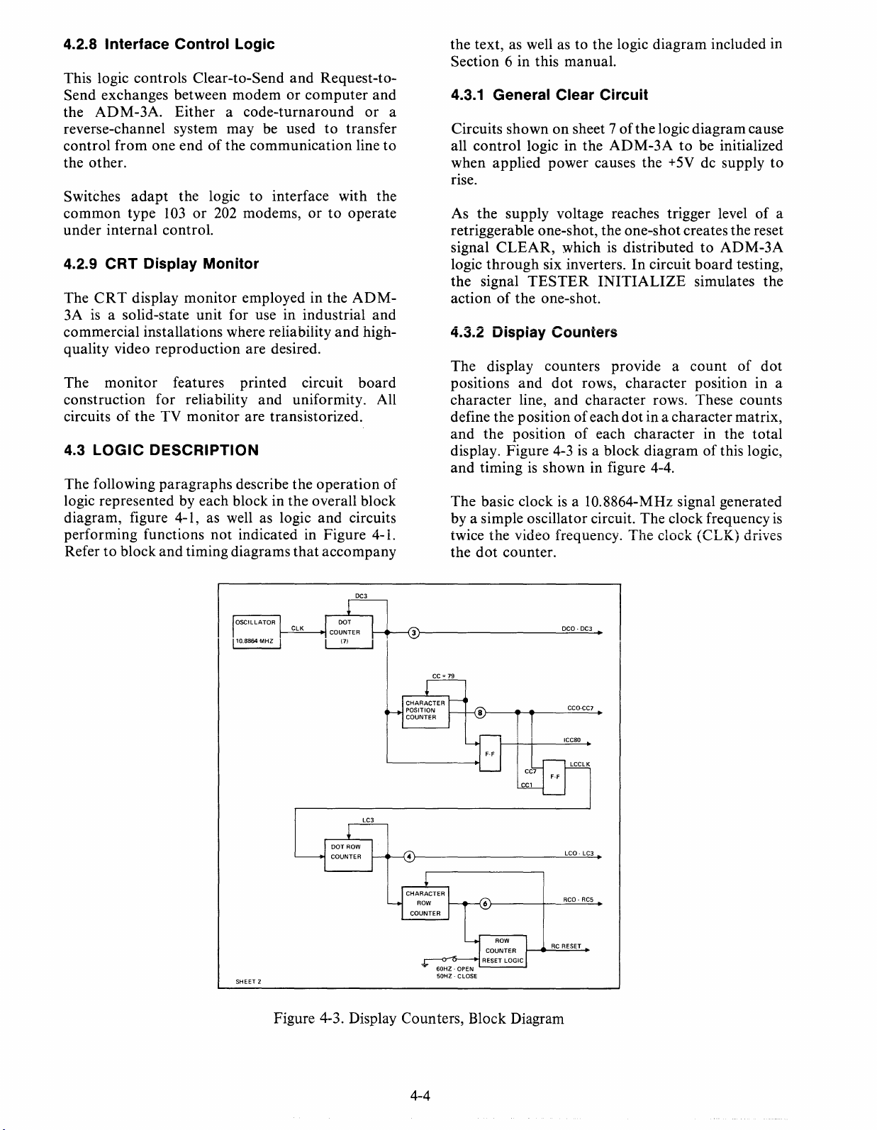
4.3.2 Display Counters
The
display
positions
character
define
and
the
the
display.
and
timingisshown
The
basic
byasimple oscillator
twice
the
the
dot
counters
and
dot
rows,
line,
and
character
positionofeach
position
Figure
clock
of
4-3 is a
is a
10.8864-MHz
video frequency.
counter.
provide
character
rows.
dotina
each
character
block
diagramofthis logic,
in figure 4-4.
circuit.
The
The
clock
a
count
position
These
character
in
signal
clock
frequency
(eLK)
of
dot
in a
counts
matrix,
the
total
generated
drives
is
SHEET 2
DC3
DCO -DC3
CCO-CC7
ICC80
LC3
LCO - LC3
RCO
- RC5
RC
RESET
Figure
4-3. Display
Counters,
4-4
Block
Diagram

CLOCK
n..n..n.IlJlJ1I
PERIOD-643.¢¢39
nsee,
FREQUENCY
= 1.5552
MHA
DC¢~
DOT
DC1~
COUNTER
DC2~
PERIOD
DC3 U 1
CC¢
CC1
CC2
CC3
CC4
CC5
CC6
CC7
LCCLK
1---------------------::::=:;::::~::::=~;:;;.77'"'T7""".7"'7""::.._r"7_J
CHAR
VIDEOSRLOAD
U
= 555.555Msee,
COUNTER
FREQUENCY=1.8¢¢KHZ
RETRACE
POSITION
COUNTER
PERIOD
= 61.7284Msee
FREQ=16.2¢<iHDKHZ
H-
DRIVE
LC¢
LC1
LC2
LC3
CHARACTER
ROW
COUNTER.
51>
HZ
OPERATION
RC¢
RC1
RC2
RC3
I-----------------------J
RC4
RC5
t--------------------------------------.....J
6¢HZ
OPERATION
RC¢
RC1
RC2
RC3
RC4
RC5
(ALWAYS
LOW
DURING
6¢HZ
OPERATION)
6¢HZ
V-DRIVE
5I>HZ
J""L
LINE
COUNTER
(DOT
ROW
PERIOD-91.8577
V-DRIVE
COUNTER)
nsee,
--.n-
PERIOD
CLOCKED
PULSE
WIDTH
H-DRIVE
CHAR
LAST
CLOCKED
RISE
24.434Msee
TIME
VIDEO
PERIOD
FREQ=5¢HZ
RISE
FREQ=6¢HZ
NOTE:
ONE
AFTER
FREQUENCY=1¢.8854
~===~
EDGES
W/H-DRIVE
= 16.667msee,
W/H-DRIVE
STARTS
(643nsee)
=2¢ms
MHZ
Figure 4-4. Display Counter Timing
4-5
The
dot
counter
comprising
to
10
overflowat15,
count,
character
position
The
eight-stage
the
positionofeach
raster
counter
character
The
character
each
at
the
count
andisagain
DC3,
clocks successive addresses
ROMs,
counter.
character
line,
and
controls
providesatotal
position,
position
79, presetsto240,
255,
and
then
wrapstozero,
CC6
are
binary
That
is,
ee7
is
low
counted,
A flip-flop
and
high
produces
countofretrace
which a
upon.
character
The
each
commandatthe
The
outputofthe
line
counter.
character
line
rowofcharacters.
counts
character.
of
the
The
zero,
presetatzero. Its final
and
triggers
position
characteronthe
horizontal
countof96 (80
and
16
count
counter
counts
counts,
through
but
CC7
while80character
during
time.
the
ICC80
retrace
signal
110 interface
LCCLK
counter
The
counts
counter
seven
dot
character
counts
through
the
counter
80-character
retrace
counts
for
the
counts
Outputs
from
the
CCO
overflow
has a valueof80.
positions
time.
ECC80
indicates
for
the
maybeacted
flip-flop clocks
the
lines
counts
columns
is preset
the
to
the
character
controls
time.
The
for
retrace).
zero
to
at
through
are
the
first
time
at
the
that
form
module
nine.
characters,
through7.The
row
The
rows
through
power
(60 EN) sets
proper
the
Counts
and
0
dot
last
and
rows
count,
8
form
are
formed
LC3, clocks
spaces between
counterata frequencyof1.8 KHz.
character
appearing
line,
time, resetting
next
row
counter
counts
verticallyonthe
vertical retrace time (six
and12counts
up
logictoproduce
character
row
for
a 50-Hz line). A switch
the
countertozerotobegin
count.
the24character
display,
counts
RCRESETatthe
by
the
character
and
for
counts
counts
a 60-Hz
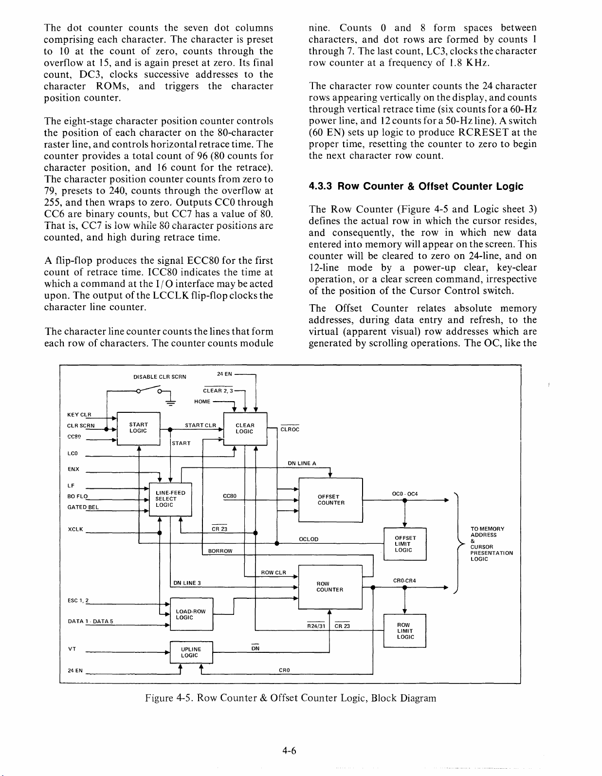
4.3.3 Row Counter & Offset Counter Logic
The
Row
Counter
defines
and
entered
counter
12-line
the
actual
consequently,
into
memory
will be clearedtozeroon24-line,
mode
operation,ora
of
the
positionofthe
The
Offset
addresses,
virtual
during
(apparent
generatedbyscrolling operations.
(Figure
row
by
clear
Counter
data
visual)
in which
the
row
will
appearonthe
a
power-up
screen
Cursor
relates
entry
row
4-5
and
Logic sheet
the
cursor
in which new
screen. This
clear, key-clear
command,
Control
irrespective
switch.
absolute
and
refresh,
addresses which
The
OC,
resides,
and
memory
to
like
1
3)
data
on
the
are
the
KEY
CLR
CC8G
LCO
ENX
LF
BO
FL
GATED
XCLK
ESC
DATA
VT
24
EN
24 EN
~
ccao
-
CR 23
BORROW
U
-
CLEAR
LOGIC
t
r
~
-
DN
f--
-+
-+
ROW CLR
CLROC
DN
CRO
LINE
OCLOD
--
R24/31
A
OFFSET
COUNTER
ROW
COUNTER
t
-
CR 23
J
OCO
- OC4
,
OFFSET
LIMIT
LOGIC
CRO-CR4
ROW
LIMIT
LOGIC
~
~
TO
MEMORY
ADDRESS
&
CURSOR
PRESENTATION
LOGIC
DISABLE
CLR SCRN
-
~
LR
C
RN
SC
0
BEL
I
-I
START
LOGIC
~I
I
START
t
LINE-FEED
SELECT
LOGIC
---
CLEAR2.3~
HOME-.
STARTCLR
~
I
i
LINE
3
DN
2
1,
1·
DATA
5
4
~
~
I
LOAD-ROW
LOGIC
UPLINE
LOGIC
t t
Figure 4-5. Row
Counter
& Offset
4-6
Counter
Logic, Block Diagram
RC,isinitially cleared by
operations noted above, however, a sequence
initiated by the
to
codes
be written into each character cellofthe
START
current row duringfirst
line-scan period. At the end
.will generate a line-feed signal,
will increment the OC. The process
OC
with the
pointing to the next rowofmemory
anyoneofthe clear-screen
is
then
logic, which causes space-
80
character-periodsofone
of
the line-scan, CC80
DNLINEA,
is
then
which
repeated;
addresses, which are also filled with space-codes.
24
After
switch
which terminatesthe
the
this point,
contain
12-line mode), and the true
such operations (12, if the 12/24 select
is
closed), the
OCLOD
START
signalisgenerated,
operation,
and
freezes
OCata countofzero (1, if in 12-line mode).
both
the
"minimum
Rowand
count" (zero in 24-line,
Offset counters will
and
and
virtual row-
addresses will be the same. (MS-A).
of
After completion
Counter
will be disabled until the Row
been advanced
Cursor
Control switchisopen
signals (DNLINEB) will be sent to the Row
each CC80 time, until a
reached. At this point, the Row
disabled until either the
closedoranother
Counter
If
Counter
operation,
Home
the same
will be enabled.
the Cursor Control switchisclosed, the Row
will remainatminimum
and
will respond to any downline, upline,
and
absolute (load cursor) row directives. In
manner
a clear operation, the Offset
or
set
to23(bottom
(ENX
true), line-feed
count
of
23
Counter
Cursor
Clearisperformed,
Control
and
count
as when
Cursor
Controlisoff,
Counter
row).Ifthe
Counter
has been
will be
switch
the Offset
after a clear
downline directives which occur when the Row
Counterisat23will be routedtothe Offset Counter,
to
causing it
by adding a difference
increment, and scroll the entire display
of
one unit between the true
and virtual row addresses.
Whereas the Offset
Counter
incremented (DNLINEA), the Row
incremented, decremented, cleared
an
absolute value (DNLINEB, VT,
LDROW).
In the event a value in excessof23
can only be
Counter
or
can be
loaded with
ROWCLR,
loaded, the counter will be cleared to minimum
count. If the Row
currently holds the minimum count,
Counterisdecremented when it
BORROW
will
occur, and the counter will be forced back to
minimum
count
generated if a
(ROWCLR).
HOME
ROWCLRisalso
(RS), directiveisreceived.
Both counters, when in 12-line mode, have the least
and
significant bit forced true,
all increment
decrement directives will affect only the higher
order
bits. In this mode, therefore, only odd virtual
that
addresses will be accessible. Note,
scrolling the
display will still produce only odd addresses, since
the Offset
Counter
will
count
in unitsoftwo, which
At
1in
has
or
when
"added"tothe odd
an
odd virtual address.
in
Row
Count
will still result
Figure 4-6 Shows the timing for the Clear Screen
or
Operation. The timing for Key Clear
is
clear operations
that
in the latter two situations,
high without benefit
identicaltothat
STARTisforced
of
DOlT.
power-on
shown, except
4.3.4 Column Counter Logic
The
Column
and
its associated logic define the character-position
of
the cursor, irrespective
mode.
accommodate
operations,
associated multiplexor, with either
values,
as the last character
The
Counter
counter
both
(figure 4-8
is
and
logic sheet
of
the current cursor
bidirectional,
backspace and forespace
andiscapableofbeing loaded, via
of
two fixed
or
a variable position-code whichisobtained
of
the
four-part
Load
4)
to
an
Cursor
sequence.
Back-spacing (count-down)
or
local
remote backspace
is
affected only by a
command
(BKSP), while
forward-spacing may be accomplished by either a
is
character-entry, a forespace
operation. All received characters will cause a
forespace afterthe character
except control characters
commandora
is
written into memory,
and
the three non-control
characters which follow ESC during a Load
sequence.
commands
CC80 time.
forespace
indicating, the initiation
The Column
For
both
character-entry and forespace
(FF), the
During
is
generated each time
counterisadvanced during
Read operations (test only), a
of
Counteriscleared in
XLOAD
character transmission.
anyoneoffour
'Read'
Cursor
occurs,
situations:
a. A Carriage
Return
received, either from the keyboard
(CR)
command
or
is
a
remote source.
b. A Home (RS)
is
c.
An underflow occurs, due to attempts to
back-space from column
commandisreceived.
O.
d. A start-sequenceisinitiated by oneofthe
power-up/ clear operations.
When the Column
80th column-count (code=79),
generated, causing
loaded into the
Counterisincremented past the
an
overflow signal
an
absolute
counter
at
count
the next
value to be
LCCLK
is
transition (CC81-time).Ifthe auto-new-line switch
is
open, a
back to the last column position.
7910
code will be loaded, forcing the cursor
If
auto-newline
is
closed, a zero-code will be loaded (carriage return)
and
a line-feed enable signal (BOFLO) will be
4-7
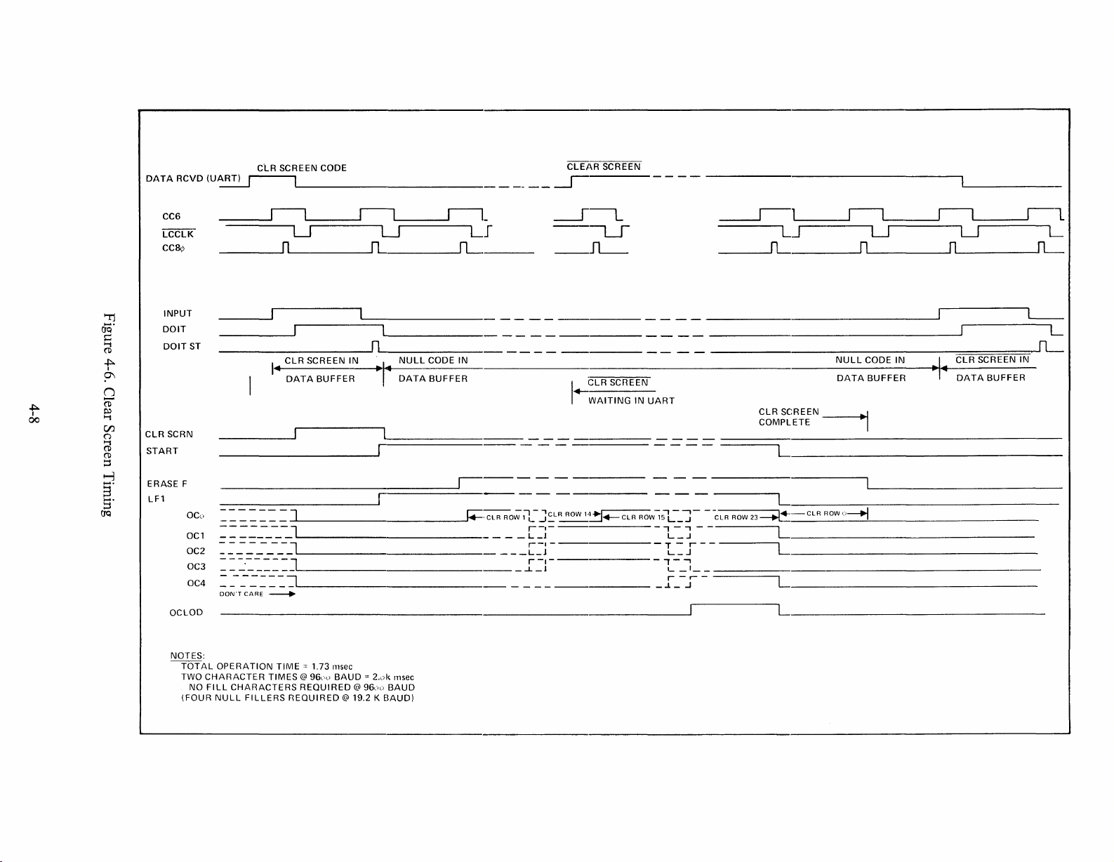
DATA
RCVD
(U~
CLR
SCREEN CODE
I
_____
CLE,lI,R SCREEN
-.-J
----
+:0-
r
00
CC6
LCCLK
cCB<,'>
INPUT
DOlT
DOlT
CLR
SCRN
START
ERASE F
LF1
OCLOD
U U
n
_________
ST
I_
CLR
SCREEN
DATA
BUFFER
_________
------~;:::::======--
:=:=
====-
===-=_-_-_-_l
OCl
=.=-
-=-
OC2
OC3
OC4
-=-_-_-
===:-=--=-==-l
=---=--==::::~I
DON'TCARE
_JL-
__
J
~
rL
--'n
1~1<ll
--1
-----f~
LJ
rL
--LJ
_IL-
I _ _ _ _ .
______
L
...
I--N-U-L-L-C-O_D-E-IN-----------------------------
I
DATA
BUFFER
l========
1
_ _ _ _ .
I
,-----
.
---Jr;:~o;~-
.J:.l~~
['=-1-
C'=-j
-
_1'=-]-
.
CLR
SCREEN
.-
WAITINGINUART
.....
:.--C-l-R-R-OW
~
- - -
- - -
-;~-_""J-
-1--=.J
-1::::
-
""L-_~
-----_._-------,
------.L
-
-C-l-R
-RO-W-2-3-~--.
- L _
J - -
------,L
_-i_-r
LJ
fL
CLR
SCREEN
COMPLETE
__
U U
n n
N_U_L_L_C_O_D_E_I_N
DATA
__
BUFFER
_I
---J
~
----====::::=:~fl.-
"_I"
CLR
SCREEN
DATA
BUFFER
L _
...__C_l_R_RO_W_'_i---.J_...!.-__. _
L _
L _
IN
rL-
'--
_
1
L
L
_
NOTES:
TOTAL
TWO
NO
(FOUR
OPERATION
CHARACTER
FILL
CHARACTERS
NULL
FILLERS
TIME
= 1,73
TIMES@96"u
REQUIRED
REQUIRED
Il1sec
BAUD
@ 19.2 K
@
=
2.c>k
96c>li
Il1sec
BAUD
BAUD)
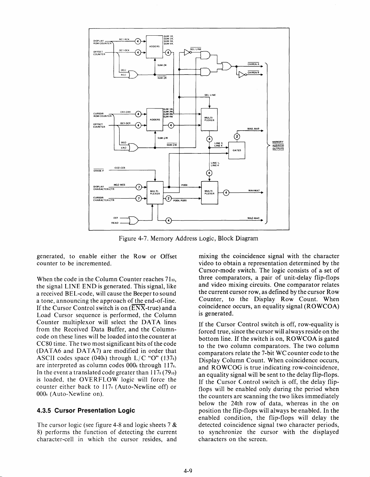
DISPLAY
-----.,...----:.R=Cl=RC4~
ROW
COUNTER
SUM
SUM
SUM
SUM
lR,
2R,
3R,
4R.
CURSOR
ROW
COUNTER
OFFSET
COUNTER
ERASE F
DISPLAY
CHARACTER
CURSOR
CHARACTERCTR
CTR
CC<1>-CC6
READ
DCO
RCO
CR1·CR4
OCl·0C4
DC""
CRO
SUM'"
SUM'"
SUM
lW.
SUM 2W.
SUM
JW.L.---+----++l
SUM
4W MULTI-
SUM'i'W
POS6
P0S4. POS5
SELLINE
PLEXER
MULTI-
PLEXER
CHIPEN A
CHIPEN
MAS.MA9
MA4-MA7
MA<1>-MAJ
B
Figure 4-7. Memory Address Logic, Block Diagram
generated,
enable either the
Row
or
to
countertobe incremented.
When the code in the
the signal
LINE
a received BEL-code, will cause the Beeper
a tone,
If
Load
Counter
the
Cursor
Cursor
announcing
Control
sequenceisperformed, the
multiplexor will select the
from the Received
codeonthese lines will be
Column
Counter
reaches
ENDisgenerated. This signal, like
to
the
approachofthe end-of-line.
switchison
(ENX-true)
Column
DATA
Data
Buffer,
loaded
and
into
the
the
Column-
counter
CC80 time. The two most significant bitsofthe
(DA
TA6
and
DATA7)are modified in
ASCII
are interpreted as
In the event a
is
counter
0008
4.3.5
The
8)
character-cell in which the
codes space (040s)
translated
loaded, the
either
column
OVERFLOW
back
throughL/C
codes
code
to I
17s
0008
greater
logic will force the
(Auto-Newline off)
(Auto-J\ewline on).
Cursor
cursor
Presentation
logic (see figure 4-8
Logic
and
performs the functionofdetecting the
cursor
order
"0"
through
than
1178
logic sheets 7 &
current
resides,
Offset
7110,
sound
and
lines
code
that
(1378)
1178.
(7910)
or
and
at
mixing
videotoobtainarepresentation
Cursor-mode
three
and
the
Counter,
a
coincidence occurs,anequality signal
is
If
forced
bottom
to
comparators
Display
and
an
If
flops will be enabled only
the
below the 24th
position
enabled
detected coincidence signal two
to synchronize the
the
coincidence signal with
the
character
determinedbythe
switch.
The
logic consists
of
comparators,apairofunit-delay flip-flops
video mixing circuits.
current
cursor
to
the Display
row, as definedbythe
One
Row
comparator
cursor
Count.
(ROWCOA)
generated.
the
Cursor
true,
the
two
ROWCOGistrue
equality signal will be senttothe
the
Cursor
counters
Control
since the
line.Ifthe switchison,
column
relate the 7-bit
Column
switch is off, row-equality
cursor
will always resideonthe
ROWCOAisgated
comparators.
Count.
When
The
WC
counter
coincidence occurs,
two
codetothe
indicating row-coincidence,
delayflip-flops.
Control
are
the
flip-flops will always be enabled. In the
condition,
switchisoff,
scanning
row
of
during
the
data,
the period when
two likes immediately
whereas in the
the flip-flops will delay
the
delay flip-
character
cursor
with the displayed
a set
of
relates
Row
When
column
on
the
periods,
is
charactersonthe screen.
4-9
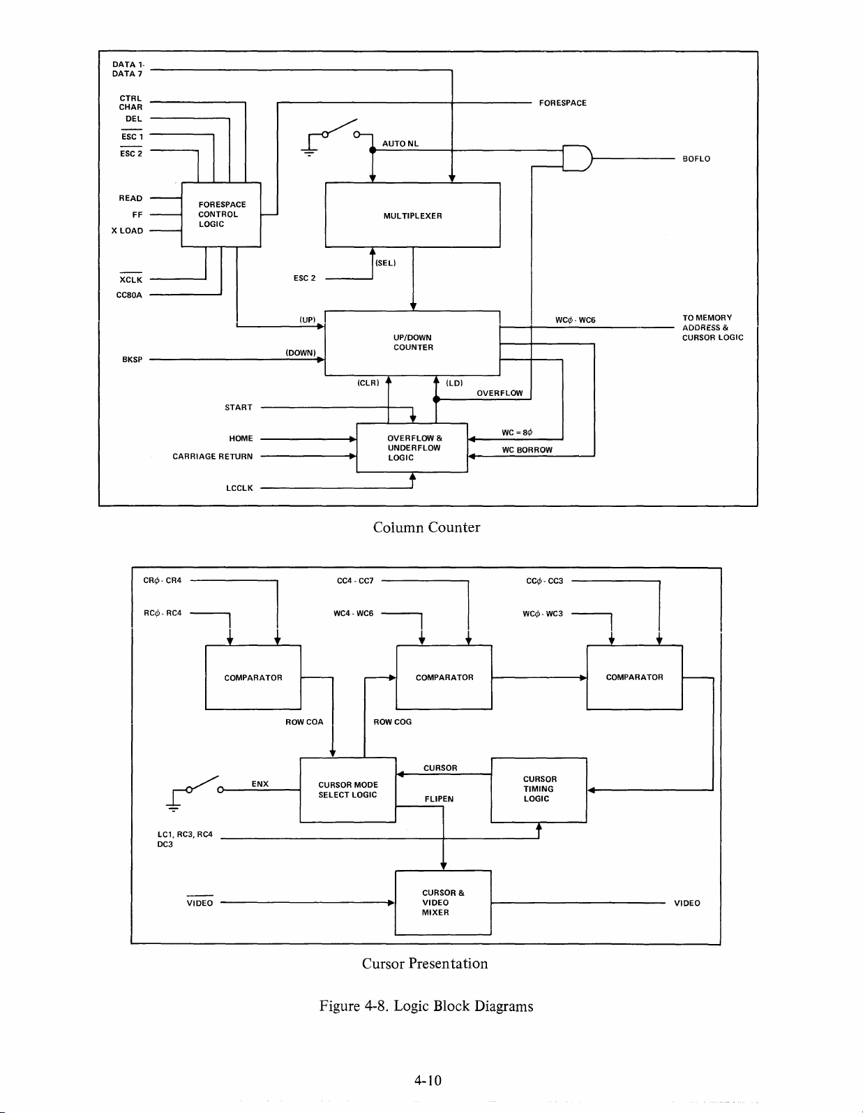
DATA
DATA
1-
7
CTRL
CHAR
ESC
READ
X
LOAD
XCLK
CC80A
DEL
ESC
BKSP
FORESPACE
1
2
~~
I
-
FF
-
-
FORESPACE
CONTROL
LOGIC
CARRIAGE
I
START
HOME
RETURN
LCCLK
I--
ESC
2
(UP)
(DOWN)
(CLR)
AUTO
11,
MUL
(SEL)
Il
OVERFLOW
UNDERFLOW
LOGIC
NL
TIPLEXER
UP/DOWN
COUNTER
+
f
BOFLO
TO
MEMORY
ADDRESS &
CURSOR
LOGIC
WC=8¢
WC
BORROW
r---LJ
WC¢-WC6
1
(LDI
OVERFLOW
&
CR.-CR4
RC¢-RC4
LC1, RC3, R
DC3
~
~
VID
-
""
C4
EO
+
COMPARATOR
ENX
I
~
ROWCOA
~
CURSOR
SELECT
Coiumn Counter
C~-~7~
WC4-WC6
~
-----.
ROW COG
MODE
LOGIC
•
~
COMPARATOR
CURSOR
FLIPEN
CURSOR &
VIDEO
MIXER
I
~
C~CO~
WC¢-WC3
CURSOR
TIMING
LOGIC
~
t
~
COMPARATOR
....-
I
~
-
VIDEO
Cursor Presentation
Figure 4-8. Logic Block Diagrams
4-10
With
Cursor
required, since the
ation
occurs
Control
during
off, no
double-underscore
the
are being displayed. With
cursor
character-video
causing the
the
coincidence signal
datainan
cursortoappear
character
in which
position
additional
mixing
represent-
period
whennocharacters
Cursor
Control
(CURSOR)isgated
exclusive-OR element,
as a reverse image
it resides.
on,
the
with
of
is
Each
cause
assume
subsequent
a successively
the
top
scroll
higher
display-row position, with
previously associated with
"rolled"tothe
The
second five-bit
Cursor
bottom
Row
positionofthe
adder
Count
operation
will,
memory-row
that
position
producesasum
+ Offset
Count
therefore,
address
the
erased
display.
equal
+ I
to
row
and
to:
4.3.6 Memory Address Logic
The
logic
group
shown
5
performs
current
the
all the functions relatedtoreconciling
entry-row
virtual row (Offset
row-address
converting
in
the
visual 80-character by 24-row visual
formattoa 64 by 30 byte
is
task
accomplished by two five-bit
full adders, while
in figure 4-7
(Cursor
Counter)
memory,
positionstoa physical
and
memory
the
secondisperformed
and
Row
array.
and
Logic Sheet
Counter)
additionally,
The
two
two-bit
by a set
multiplexors.
The
first five-bit
Display Row
function
This
between
address
data
current
during
might be displayed
adder
producesasum
Count
provides
display rows
+ Offset
the
required relationship
and
refresh scanning, in
on
the
proper
equal
Count
+ I
the virtual row-
order
that
rowofthe
screen, consistent with the scroll-history since
last clear-screen
occurred, the offset
the
top
row
memory-row
display-row
data
for the
row
zero. Oneofthe two-bit
gates,
greater
performs
than23to a 24-row universe, by
appropriate
o+ I =
If
top
I =2)and
24~0).
the display has been scrolled one time,
row
will be
data
row I, thus, it can be
in
memory
the display by one row,
even
though
is
unchanged. The only physical
example, occurs in
(see section 4.3.8)
leaving
for new
the
new
data-entry.
operation.
count
of
the display will be
If no scrolling has
will be zero,
and
obtained
I (0 + 0 + I= I). Likewise,
22
will come
bottom
from
row will
memory-row
come
from
adders,
plus associated
the functionofreconciling sums
adjustment
obtained
for the
will
appeartohave moved
its
actual
factortoall such sums (23 +
from
memory-row2(0
bottom
demonstrated
after
physical
row
from
that
the scrolling
locationinmemory
alteration,
memory-row
during
bottom
row address locations clear
I, which is erased
the
scroll
data
data
23,
memory-
adding
data
for the
memory-
all the
upward
operation,
in this
operation,
and
first
of
to:
the
the
for
at
for
and
an
+ I +
data
on
function
This
position,
must
appear
which determines
erased
and
scrolling
row,
the
the
desired
is
row
from
row
of
refresh.Ifthe
bottom
24
gate
greater
is
data
row,
~
0),
set which reconciles all
than23to
consistent
entered
routedtomemory-row
As scrolling occurs,
maintains
cursor
that
row
time as
position
data-entry
whichisdisplayed
the
reconciles
which is
on
rolledtothe
has
occurred
resultant
row
which
the
duetothe
with
under
the
cursor.
the
current
the
rowonwhich new
the
display,tothe
the
last
memory-row
bottomofthe
and
the
sum
for
data
will be
will be
memory-row
data-entry,
obtained
cursor
sum
would
be zero (23 + 0 + I =
actionofa second
CR+OC
values between 0
the
refresh adder-set, since
these
circumstances
zero.
the
second
proper
and
will always
relationship
the
virtual
occurinthe
during
Considerasanother
scroll-history,
cursorison
since
were
movedtothe
and
display-rows,
the
same
display which has been scrolled six rows,
the
cursorispositionedtorow
actually displayed
Ifan
entryismadeatthe
same
summation
and
Offset
Counter
madeinrow
The
multiplexor
manipulates
Logic
derived above, plus
Display
Column
Column
Counter
the 80 x 24 display
matrix.
The
on
row
+ 6 + I =
20
will
occur
values,
3.
sectionofthe
the
CR+OC
the
Counter
(WCO - WC6) in
matrixtoa 64 x 30
first-stage
between Refresh accesses
accesses, since
OC
sum
latter
are
the
former
and
the
CC
Counter
governedbythe
20.
The
20 will be:
27~3
current
cursor
using
and
Memory
and
information
(CCO - CC7)
multiplexors
to
memory
are
governedbythe
information,
CR+OC
the
the
RC+OC
ordertoresolve
sum
counter.
The
time-period
display-time
for
when
each
CC7isfalseisthe
scan-line,
and
cursor
row-
data-entries
that
was
display.Ifno
the
top
I, which
thatisthe
for
the
top
adder
+ 1
and
sums
23. This also
any
will be
adder
between
group
the
such
memory-
row-scan
example,
after
which
memory-row
position,
Cursor
entry
the
Row
will be
Address
sums
from
the
and
Cursor
memory
distinguish
and
write
RC
while
the
and
the
WC
active
therefore,
a
+
4-11

defines Refresh-access time.
retrace, when CC7istrue, the
for
data-entry.
During
test read-back, thefirst-stage
multiplexorislocked into the
During
memoryisavailable
"Write"
ordertoexpedite the transferofinformation,
not
display functions are
necessary
horizontal
mode in
since
during
this
operation.
The
most
significant pOSItion
of
the
CCI
WC
multiplexorisused as a selection signal for the
SUMRI
phase will always cause selectionofSUMW
OC) for the
functions.InRefresh mode the
outputs
Clear
operations
the
place
total
SUMW
multiplexor,
and
LINEI-LINE4
SUMR
will normally be selected, however,
Screen
SUrv1Vv'
during
time required for such
or
the
term
terms, in
CC7 time
Line Erase (when scrolling)
ERASEF
order
will force selection
that
all erasures
and
thereby minimize the
operations
in the write-
and
Chip-Enable
(RC
(See Section
(CR
+ OC)
during
can
take
4.3.8).
The selected low-order
require
no
additional
smallest increment
column
terms (MAO - MA3)
modification, since the
of
memory
allocatedtoa given
of
lineis16
terms
terms
to
account
memory
final multiplexor stage uses the
to
distinguish between column-positions greater (or
equal
the high-order address functions
derived from POS4,
respectively. This
+
relationship between a 24 x 64 section
and
23
and
POS6
MA
MA8
section
the 24 display rows, by allocating
characters. The three high-order column
(POS4
(LINE
- POS6)
and
the
four
high-order row
1- LINE4), however must be modified
for the
matrixof64
maximum
column-widthofthe
characters. Accordingly, the
column-term
to)
and
less
than
64.
For
positions less
MA4
POS5
translation
that
portionofthe display defined by 18WS 0-
columns 0-63.
For
& LINE1 - LINE4
provides a direct
column
positions 64-79,
than
- MA9 are
of
memory,
switches the multiplexor to derive MA4 -
7 from
LINE
and
MA9 true. This
of
memory
1- LINE4, respectively,
translation
relates a 6 x 64
to thelast16column
and
positions
one-quarter
POS6
64,
forces
of
of
each memory-row, progressively, to the remainder
of
each display row. The chip-enable functions
and
odd
define even
groups,
and
organization
on
figure 4-9.
display rows
therefore, requirenotranslation. The
of
display
data
in memory,isshown
and
memory-
" _
80 CHARACTER COLUMN ADDRESSING
SEQUENTIALLY
ROW
& COLUMN
ADDRESSING IN
THIS
AREA
NORMAL
iNCREASE
ARE
ROW
ROW=15
ROW
ROW=17
ROW
ROW
ROW
ROW=21
ROW
ROW=23
ROW=6
ROW=
ROW
ROW
ROW
ROW=11
ROW =
ROW
= 16
= 18
= 19
= 20
= 22
ROW=O
ROW
ROW
ROW
ROW=4
ROW=
= 9
= 10
12
= 13
=
14
= 8
-------
7
r-
ADDR'"
SW"CH"
IN THIS
AREA
(COLUMN
....
•
~I:I~I
~
I~I~
I~
I~
1;1
ROW
= 1
= 2
= 3
I;
5
ROW
0
ROW
1
6
1
ROW
6
ROW=24
ROW
ROW-24
ROW
ROW
ROW
ROW
i
6
ROW=27
1
6
ROW
3
2
ROW=27
3
2
ROW
4
8
4
ROW=27
8
ROW
ROW
0
ROW
1
6
1
ROW
6
3
ROW
2
ROW
3
2
4
ROW=28
8
ROW=29
4
8
----l
>63)
~ I~I~I
~I~I
~I
~I~
= 24
= 25 1
= 24
= 25
- 25 4
= 25
= 26
= 27
= 26
= 26
= 26
- 28
= 29
= 28
= 29
- 28
='29
• 5
• 5
• 1
• 1
iJ
• 7
• 3
• 3
• 5
• 5
•
• 1
• 7
• 7
• 3
• 3
• 5
• 5
•
•
• 7
• 7
• 3
• 3
1
3
3
4
7
6
6
1
1
3
1
3
4
4
6
6
1
1
3
1
3
1
4
4
6
6
MEMORY ADDRESS
(SCHEMATIC
I
NOTES:
1,
BiT
WEIGHTS "
MA9
ROW
MA8
ROW
MA7',
ROW4
MA6
ROW
CHIPEN
MA5
COLUMN
MA4
COLUMN 16
MA3
l"ULUJI,'Il'\l
MA2
COLUMN 4
MAl'
COLUMN 2
MAO COLUMN 1
2,
SCREEN
ACTUALLY
30 LINES x 64 CHARACTERS,
3,
ADDRESS
MANIPULATED
ADDRESS INCREASES ABOVE 63,
SHEET
16
8
2
ROW
1
MANIPULATION
4,'1ONE
ell
32
0
ORGANIZED
WHEN COLUMN
l
AS
Figure 4-9. Organization
of
Display Data in Refresh Memory
4-12

4.3.7 Refresh Memory and Character
ROM Logic
Figure 4-10 shows logic comprIsmg the refresh
and
memory, buffer latches,
character memory
ROMs.
The refresh memory
semiconductor
RAM
is
made
up
devices in one
of
2K, 7-bit
of
four
configurations as follows:
a. Six
RAMs
for upper-case only, 12-line
display.
b.
Seven
RAMs
for
upper
/lower-case, 12-line
display.
c.
Twelve
RAMs
for upper-case only, 24-line
display.
4.3.8 Erase Logic
A display lineiserased by the Logic shown
Schematic pages 3
The
ERASEF
SETERA
describes the condition in which
PGMOD&LFI
to begin counting
line-feed
is
and
4.
signalisturned
on
by
are true, causing the offset
and
the lines to scroll each time a
caused by the column
SETERA.
on
both
counter
counter
overflowing (BOFLO).
ERASEFisturned off by CC80A after a single
character row has been cleared, during scrolling.
However, when
Code,
turned
ERASEF
off by
STARTisraised by a
remains high until
an
overflowofthe offset counter.
Consequently the entire screen
is
CLR
erased.
SCRN
START
is
d. Fourteen
RAMs
for
upper
/lower-case, 24-line
display.
A switch (UCEN) sets up the logic to operate with,
or
without, the lower-case RAMs. UCEN alters
datatoadapt
case only)
ERASEF
creating a
NULL
Data
from the input buffer
loaded into,
address lines MAO-MA9. The memory
for each character time, by
CHIPENAis
from,
data.
RAMs
CHIPENB
the logic for either 6-bit codes (upper-
or
7-bit codes (upper
causes the logic
SPACE
code in placeofthe received
/lower
to
force bit 6 high,
code.
(DATA
or
read from, the refresh memory by
WRITE
low as
storing the
dataisloaded into,orread
12
odd linesofdisplay
enables the
RAMs
case). Term
I-DATA7)is
is
clocked,
PULSE.
storing the
12
even lines in a 24-line display.
At the end
of
each character period, DC3 clocks
an
addressed character into buffer latches which store
the character to be encoded by the ROMs. The
buffer latches are cleared by
is
Because CBUF6
SPACE
code,
normally inverted, however, a
rather
than
NULL,ispresentedtothe
VIDEO
BLANK.
ROMs.
4.3.9 WRITE PULSE Logic
The
WRITE
(RAM)
PULSE
memory. Logic
signal clocks the refresh
that
generates
WRITE
PULSEisshown in sheet 4ofthe logic diagram.
WRITE
dot
FORESP
ERASE
PULSE
count
DC2,
ACE (the
LINE.
consistsofgated pulses clocked by
and
is
normally gated
inputofthe cursor counter)
on
by
or
The non-destructive space code feature allows
writing a
SPACE
code
(0408)
into the
RAM
memory any time between a Line Feed (LF) code
and
a Carriage
SPACE
LF
inhibited betweenthe
code. This permits the
write a displayonthe screen, issue a
Return
(CR) code, with writing
CR
code and the next
computeroroperator
CR
code,
of
to
and
space over the previously written data, with the
cursor, without writing over the data.
NO
The
WRITE
write signal inhibits
PULSE
is
not
FORESP
ACEsothat
generated during
that
period. A switch permits inhibiting the nondestructive space code feature.
4.3.10 Keyboard Logic
Two
a 5-bit
ROMs
output
decode
code
CBUFn
that
provides the
characters and produce
dot
pattern
for
each line in the character matrix. Each of the seven
is
lines in the character matrix
count
output
LCO-LC2. The parallel-bit information
by the
ROMsisserialized for presentation
identified by the line
to
the video monitor.
One
ROM
contains upper-case characters,
and
the
other contains lower-case characters. Select logic
of
senses states
CBUF6 and CBUF7 to enable either
ROM device.
CBUFnisavailableatdata
transmitter logic for
transmission in read-back test operation.
Keyboard logicisshown
on
sheet 9ofthe logic
diagram (except for lock!unlock logic shown
sheet
10).
Timing
of
keyboard logic functions
shown in figure 4-11.
The keyboard
complete sequence
speed,
and
is
encoded by generating the
of
7-bit
USASCII
trapping the code
that
depressed key. The codes are generated continually
is
and repetitively unless a key
is
sequence
is
the gated character rate signal
clockedata
counter
pressed. The code
by KBCLK, which
CCO.
The four least-significant bitsofthe
KC4) encode the
rowsofthe
USASCII
16
4-13
on
codesathigh
matches a
count
(KC1-
code
is

DATA
(OPEN FOR
LOWER CASE) ICEN
7
RAM
(UPPE
R/lOWE
CASE ONLY)
R
f---+
RAM
(UPPER/lOWER
CASE, 24-L1NE
MODEL ONLY)
~
LCO-LC2
DATA
DATA
UCEN
ERASE F
DATA
MAO-MA
WRITE
CHIPEN A
CHIPEN B
7
6
1 -
PULSE
DATA
9
UC/ULC
~
SELECT
LOGIC
i i i
~
RAMS
6
t
5
-®--+
-@)--.
f---+
-----.
--..
6 RAMS
(24-LINE
MODEL
ONLY)
L
BIT
-
T
BITS 1-5
UC/ULC
}--
SELECT
6
LOGIC
LATCHES
-®-+
DC3 i r
VIDEO
ClK
BLANK
1 i i
CLR
C BUF 7
C
BUF
6
C BUF1-C BUF 5
UC!ULC
SELECT
LOGIC
CHAFlACTER
BITS TO
VIDEO
UCEN
LCCE
~
-®-+
SERIALIZER
if
ROM
(lOWER
CASE) IUPPE R
T
-
------
------
f
ROM
CASU
~
I
SHEET 7
Figure
4-10.
Refresh
Memory
and
Character
ROM Logic,
Block
Diagram

n n n
-J
RC2
KEY
DATA
BIT
SET
GO
BOUNCE
A-OUT
B-OUT
C-OUT
D-OUT
~
I
-
VI
SHIFT/LD
X
LOAD
LOAD
X
REPEAT
FLOP
l......I L.....J
----------'
__________
------------
------------
-------------+--------:R::-:E::-:P:"::T:-:D=-E=-:P::-:R::-:E::-:S:"::S:-=E-=D'--='-
4.44ms
~~';:'ri
~
I
I I I
SCANN
ING
---1
.......
f-::D:-:E::-:B:-:O::-:-U-:-::N-:-:C:-:E::--
FAST
CLOCK
---------.
I
r-
1¢.288/-'s
- 1 I -
~
n)
I
I
5pHZ28
6<.~HZ
RC2-RC
RESET
16ms
ms
~I
KEY
>
I
J
" KB
I
RELEASED
CIRCUIT
'1'\
I
s-L
'-
1
----ll
n
II
L_________________
----In
b
-.rl+-
(~r""',
-' _
..
~i""·--------:-:W-:-:A:-:I=T-:-:1
N-:-:G=-=F-=O-=R-------+~
REPT OR
........
--------------:S:-:-L-=O:-:-:W"7"C-::-:-LO=-C=-K::-------------------------i~
RELEASE
.......
f----------=-R=Ep::-E::-A-T-I-N-G---------------
n
L-
II
LJ
I
59
HZ-
&,-...HZ\
r--l
I L JF
~~
I,
I
L-J
l¢cps
12cps
.
~
.--------,
L-.J
fL-
.....
f------
I
r--
.....
t---SC-A-N-N-I
f---F-A-S-T-CLOCK
RESET
NOTE:
KEYISRELEASED
DURING
IS
COMPLETED
TERMINATING.
IF
RELEASED
D-OUT,
TERMINATED
N--=-G
D-OUT,
CYCLE
BEFORE
BEFORE
CYCLE
IS
IMMEDIATELY
I
Figure 4-11.
Keyboard
Logic Timing

chart.
the eight
the
logictocount
of
the
The
three remaining bits (KC5-KC7) encode
columnsofthe
chart.
Whennokeyisdepressed, KEY
KBCLK
BOUNCE
KEY
KBCLK
KEY
has
At
BOUNCE
immediately rises
key, however, the high
RCRESET
cycles the
high. When a keyisdepressed
corresponding
OAT
A falls, preventing
pulses so
DATA
also causes
900HJ
completed
the
a 5.56-msec delay period.
end
of
becomes true, inhibiting
RCO.
keyisheld
If the key
down,
pulses (at the ac
counter,
code
that
and
appearsonlines KC
the codeisheldonKCn lines.
GOtorise, causing
RCO
pulses until a fifth pulse
the key-bounce delay period,
is
released, KEY
and
counter
along
with the REPT(Repeat)
BOUNCE
power
DATAishigh
bounce
logic holds
and
l-KC7,
generationoffurther
bounce
further
counts
DATA
cycling resumes.
signal permits
line frequency)
to clock the bounce delay period, generatingthe
signalata rateof12.5
or10characters per secondata 50-Hz line rate.
Hz,
Consequently,
until
either
The
term
of
the
selected
longer
than
When the
and
KC7A are forcedtozero, forcing
code
into
the
keyisreleased.
TH
RE limits the repeat rate if the period
baud
the repeat cycle.
CTRL
column0orIof
Bit KC5A selects either
column
I (when true).
keyispressed (0110010)
effective code becomes
With either S HIFTkey depressed, bit 6
inverted
(USASCII
Also,
to
select upper-case
column4or5,insteadofcolumn6or
INVERT
5 selects codes in
2 insteadofcolumn3,to
on
symbols
and
COL3identify those codes in the shift logic.
Row
numeral
0 codes in
excluded from this
"upper
case" functions.
TheUPPERCASE
include the lower-case
is
depressed, useofthe
key
on
alpha
keys. Lower-case
in
USASCII
term
KC6 KC7 causes
columns6and7.Therefore, the gated
upper-case codes
Other
KC7
and
The
that
codes in
SHIFT
down.
BREAK
the
columns4through7are
EN which permits
keyisdepressedtosignai the
operator
characters
per secondat60-
characterisrepeatedatthat
rate creates a
character
(control) keyispressed, bits KC6A
any
generated
the
column
For
example,
along
control
USASCII
0 (when false)
code
code
when the "2"
with
CTRL,
DC2
(00 I00
(KC6A)
encode
and
symbol
columns2and
action
because they have
keyisused in units
alpha
characters. When the
SHIFT
alpha
INVERT6
without
useofthe
alpha
USASCII
keys.
3 (S P
codes are encoded
characters
column
the "upper-case"
Terms
and
thatdonot
key has no effect
to
maintain
SHIFT
identified by
normal
shifting
computer
wishestoterminate
data
transfer.
and
then
GO
rate
time
chart.
or
the
10).
7).
COL2
0) are
no
key.
up
The
Break functionismaintained
keyisheld
interface
data
transmit
down.
control
linetothe
The
logic where it forces the
transmitting,orforces
to
the
"mark"
interface
is
state if
in
the
dataisbeing received
secondary-channel
signal
"space"
the
secondary
for as long as
BREAK
state if
transmit
appears
primary
the
unit
and
mode
the
at
is
line
the
of
operation.
When
the
CLEAR
keyisalso depressed
keyboard
interface
The
Back
If
to
be senttothe
characters
Either
command
IDENT
lock logic,
control
HERE
IS key activates
function
long,iscontained
the level
received
signaltoactivate logiconthe
key is pressed,
(SHIFT
the
refresh
EN),
and
KEY
memory,
the
CLR
SHIFT
clears
and
logic.
an
optional
Answer
which causes a unique, fixed message
computer.
from
the
from
The
HERE
the
computer,
message,upto
in a
PROM
IS key,oran
device.
causes
32
ENQ
the
Answer Back
board.
Keyboard
to
enable
KBLOCK
CLR,orby the decoded
reset-enabled by
Keyboard
DOlT
keyboard
KBLOCK
lock logic (sheet5)permits
or
disable
the
keyboard
signalisset-enabled locally
UNLOCK
the
decoded
lock logic by CC80.
from
generating
LOCK
KBLOCK
GO, inhibiting
action. A switch permits
true
regardless
of
the
logic.
command,
command.
received
computer
The
by
KEY
and
prevents
any
holding
LOCK
commands.
4.3.11 Beeper Logic
is
Beeper logic (sheets 3 & 4ofthe
producesanaudible
The
signal
that
row
rate
LC2, which has a rateof3.6 KHz.
The
rate LC2isenabledtothe
"on"
periodofa
triggered
on
characteriswritten in
WC3 WC6).
The
codeisreceivedatthe
Because a
code, the
so
that
read-back
term
the BEL
signal as a near-end warning.
drives
by
the
one-shot
WRITE
any
speakeristhe
circuit.
CHAR
line (WCO
one-shotistriggered when a
I/O
interface.
operationisinitiated by
READisusedtodisable
code
cannot
logic
speaker
The
cause
diagram)
character
during
one-shot
as
the
WCIWC2
the
one-shot
the
audible
the
is
7lst
BEL
BEL
signal.
The
OVERFLOW
shot
when a
Because
baud
the
the period between successive 7 Ist
case,
the
beeper wuuid utherwise
continuously
signalisusedtoturn-off
rate higher
periodofthe
while
dataisbeing received.
than
one-shotisgreater
2400
baudisused.
characters
remain
the
one-
than
in this
energized
4-16

4.3.12 Data Receiver and Command Decoder
Logic
This logic (figure 4-12, schematic 6 &
data
from the computer
through
either a
10)
receives
standard
RS232 interface,ora current loop interface. Serial
dataisreceived
RS232 receiver which sends the
circuit which also receives
through
the RS 232 interface by
data
to
an
data
from the current
an
OR
loop receiver.
TO
EXTENSION
RECEIVED
DATA
(RS 232)
>--...--.J
PORT
UNiVERSAL
TRANSMITTER
RECEIVER
(RECEIVER
SECTION)
(UART)
DOlT
DATA
RDY
is
The current loop receiver
to
responds
current in either direction. The receiver
a bipolar circuit and
comprises a rectifier/limiter which drives
and
coupler,
the optical coupler.
the amplifier
furnishes the
A third input to the
transmitted from the
appears if the
lATCHES
(ClK)
a single-transistor amplifier driven by
If
the RS232/CLswitchisopen,
output
UART
HDX
DATA
~.------~
appearsatthe
OR
input.
OR
logic
is
ADM-3A
(XDATA)and
(half duplex) switchisclosed.
1 -
DATA
7 TO
DECODER
LOGIC
REFRESH
MEMORY
DECODED
COMMANDS
an
logic
data
optical
that
being
SHEET
CLEAR
ERASE F
CCG
lCClK
6
INPUT
TIMING
lOGIC
Figure 4-12. Data Receiver Logic and Command Decoders
The received serial data, from whatever source,
clocked into the
UART
by RECV CLK (at the
selected baud rate). In the UART, each received
is
character
stored and presented in parallel-bit
form to latches, with the most-significant bit
appearing
the IN7 line. (lN8isnot
used in the
on
ADM-3A.)
The character stored in the U
latches by
UART
INPUTasDATA
(unless
ERASEF
inhibits INPUT).
ARTis
RDYisoutput
clocked into
by the
INPUT
rises when CC6 occursattheendofevery horizontal
scan. Then LCCLK turns on
on
for the next full horizontal scan period during
which the last received
data
The
character stored in the latchesisdecoded
DOlT,
commandisexecuted.
which remains
to obtain the different control command signals.
The three least-significant bits are used as chip-
enable codes and are made effective by
DOlT.
Consequently, control commands are not effective
until execution time.
INPUT
ClR
BUFFER
is
4.3.13 Data Transmitter Logic
Data
transmitter logic
(schematic sheets
8,
is
shown in figure 4-13
10&12).
applied to the transmitter section
a.
Keyboard characters KCn, and the
signal from keyboard logic, when
Data
that
of
the UARTare:
READ
may be
XLOAD
is
false (normal operation).
b. Characters
applied
optionisincluded in the ADM-3A,
back
of
through
the answer-back message,
KCn
lines, when the answer-
and
READisfalse.
c.
The contents
(CBUFn) when
of
the refresh memory buffer
READistrue (in read-back
test operation).
UART
The
the gated
logic and
loaded from
XMIT
XMIT
CLK
CLK
is16times the
XDA
TAn lines by LOA ART, which
that
clocks the
selectedatbaud
baud
rate. The UART
UART
rate select
is
is
is
normally high.
4-17

r----
I
KEYBOARO{
LOGIC
I
IMEMORY
BUFFERS
I
~H~
XLOAD
KC1-KC7 7
CBUF1·CBUF7
READ
STOP BITS
WD
PARITY
pARITY
BIT
8 CONTROL
----,
C
I
LOA
MUL
TIPLEXER
ART
I-X-D-A-T-A-1-_--.....
X
DATA
7
~
~L-------r-_..I
I
I
_
LENGTH
ENABLE
INHIBIT
_-.J
(OPEN, 2 BITS)
(OPEN, 8 BITS)
(OPEN, EVEN)
(OPEN, NONE)
MARK
(OPEN,
1)
-
UART
XMIT
CLK
-------------------tTRANSMIT
UNIVERSAL
ITRANSMITTERI
RECEIVER
(UART)
(CONTROL
SECTION)
TRE
I---·--------
THP~
CLOCK
LOGIC
.....
SHEET
RTS
IRS
XMIIT
CLK
f+--.-------------«
12
232/CL
CLR TO SEND
CURRENT
TRAN~
MITTER
BAUD
RATE
SELECT LOGIC
t--------t~
LOOP
XMIT
DATA
RS
232
INTERFACE
CURRENT-LOOP
LINES
~
<
RS
232
INTERFACE
10
SHEET
Figure 4-13.
Data
Tr~mitter
Logic, Block Diagram

The
UART
SEND
controlled by TRE.
the UART.
holding register in the UART.
(which
TREishigh. With the holding register full
serializer empty, the U
the character into the serializer. At this time
rises, ready to accept the next character,
falls to indicate
THRE
XMIT
appears
THRE
is
loaded from the holdingregister)isempty,
CLKisenabled when
at
the interface,
TRE
and
THRE
falls when
XDATA
If
CLR
and
further
are
output
loads the
the serializer
and
AR
T automatically transfers
THRE
and
that
the serializerisbusy. Both
and
TRE
are high when the UART holds no
TO
by
the
TRE
data.
is
Transmit clock logic
reset by the next Request
Send(RTS) signal from the interface.
Five switches permit formatting the transmitted
is
character. First transmitted
followed by the seven
parity bit, odd
followed by one
or
or
The serial bit stream
data
even,
two Stop bits.
is
ORedtotransmitter circuits
always the
bits (LBS first). The
then
follows (if enabled);
through a gate which also receives
appear
(from
another
device)atan
data
Start
bit,
which may
extension port.
to
If
the
BREAK
lineisforcedtothe high
Dataissent
loop interface, depending
RS232/
CL
keyisdepressed, the
(SPACE)
through
either the RS232orcurrent
on
XMIT
DATA
level.
the positionofthe
switch. The unselected interface
maintains a marking level. The RS232 interface
comprises a simple driver. The current loop
interface uses
data
to
an
output
networktothe current loop.
optical couplertocouple the
amplifier,
and
then
through
TTL
a diode
an
The optical coupler completely isolates the current
of
loop transmitter from the ADM-3A. One leg
current loop may be tied through a register to
to
create a current source.
dc
ground strap may be used instead
Asanalternative, a
of
the resistor,
the
+l2V
to
act as a sink foranexternal positive source,ora
an
current source for
external negative voltage.
4.3.14 Video Blanking and Serializer Logic
Logic
that
controls blanking during horizontal
and
vertical retrace time, and converts the parallel-bit
ROM
outputs to a serial bit stream,isshown in
figure 4-14.
CC7
POS15
RC5
RC=24/31
RCO
24
EN
DC3
READ
CHARACTER
ROMS
_DC_3
__
ClK
CLEAR
2
~
VIDEO
~
BLANKING
lOGIC
~
~
BITS
-+t
lD
SHIFT
(VIDEO
~
'---------~CURSOR
J--V_I_D_E_O_B_lA_N_K_
FROM
REGISTER
SERIALIZER)
ENX
CURSOR
ENX
......TOC
lATCHES
BUF
FLIP
EN
MONITOR
VIDEO
+--+
SHEETS 7
TO
VIDEO
MONITOR
& 8
Figure 4-14. Video Blanking and Serializer Logic, Block Diagram
4-19

Terms CC7,
. row countsof32
when the
50-Hz (the
operation).
POSI5,
and
and
RC5 control blanking for
higher,
and
are effective only
ADM-3Aisoperatingata vertical rate
count
For
reaches only
29
in 60-Hz
counts below 32, term RC=24/31
controls blanking.
RCO
and
Terms
character rows
24EN cause all even-numbered
to
be blanked if the
ADM-3A
operating with a 12-line display.
In
every case,
VIDEO
BLANKisclockedtothe
memory buffer latches by BDC3 as the current
is
character
completed.
buffer latches but, because bit 6
inverted, the
USASCII
VIDEO
SPACE
BLANK
clears the
is
normally
codeispresented
the ROMs, insteadofNULL.
During
the video
a read-back test operation,
but
permits sending
READ
CBUFn
blanks
data
transmitter logic.
The video serializer
DC3 loads it with the
every 643 nsec,
of
rate
ORed
10.8864 MHz. The shift register
with
cursor
MONITOR
adjustment potentiometer
isan8-bit shift register.
ROM
and
the bits are shifted (by CLK)ata
output
character
information to produce the
VIDEO
signal. The video level
is
located
Term
output
at
these
circuits.
of
to
to
bits
4.3.15 Monitor Drive Logic
This logic (shownonsheet 7ofthe logic diagram)
that
generates signals
drive cycles in the monitor. To
drive signal
decoded
HD
RIVEisset true one
start
is
to
HDRIVE,
to
set
HDRIVE
the video retrace period.
The vertical drive cycle
is
signal
counts RCn,
count
generated by decoding character row
and
after the lastcharacterofthe lastline has been
written. The flip-flop
signal for the line
trigger horizontal
obtain
character position counts are
falseatthe startofa row.
count
after the riseofCC7
is
begun by VDRIVE. This
setting
just
theVDRIVE
is
clocked by the
completed.
The level 60EN controls timing for 50-Hz
and
vertical
the horizontal
flip-flop one
HD
RIVE
or
60-Hz
power lines. Refer to figure 4-4 for timingdiagrams.
is
4.3.16 Baud Rate Select Logic
Figure 4-15 illustrates the logic used to generate and
select
baud
rates for
data
transmission and
reception.
DOT
COUNTER
SHEET 10
DCl
(3.1104 MHz
1800
BAUD
BINARY
COUNTER
~ 16
(-;-.9 FOR
1800
I
ClK
e---+---+--+--+---+
BAUD
RATE SELECT SWITCHES
BAUD)
1
BINARY
COUNTER
-;-.5
(-;-.6 FOR
1800
BAUD)
4
ClK
2-
ClK
5
e_----+
_-+-
__
4 4
DOUBLE CLOCK
REMOVE JUMPER (ETCH)
FOR SPLIT
TRANSMIT
CLOCK
BINARY
(
711
g SELECT FOR
0 SPLIT
o CLOCK
....
0
o
o
0
o
COUNTER
-;-.16
FOR
TRANSMIT
110
110BAUD
BAUD)
RECV
XMIT
ClK
ClK
Figure 4-15. Baud Rate Select Logic, Block Diagram
4-20

The
basic clock used in this logicisthe 3.1104-MHz
pulse
stream
dot
counter. The 3 binary counters divide pulse rates
5,16and16respectively except whenan1800
by
110
baud
19,200
selected by meansofa
baud)
DCI,
which originatesatthe display
rateisselected. These rates
are obtained
from
BAUD
the counters
RATE
(from
Switch.
and
or
75are
e.Ifonly the 202 switchisclosed, RTSmay
controlled
either
operation.
through
code-turnaround,
the
ADM-3A
or
reverse-channel
interface
be
in
When
counters divide pulse rates by 6, 9
respectively
clock.
When BA UD
divide the pulse rate by
CLK9isselected as the
The
provide the
signals. Normally,
same rate. However, when a split clock
the
rate selected by meansofa
inside the
must be in position
the printed circuit joining clock inputs
flops must be cut.
BAUD
double clock rateisdivided by flip-flips
XMIT
When the
NOTE:
RATE
and
CLK5isselected as the
RATE
RECV
CLOCK
ADM-3A
common
XMIT
the
RECV
or
1800 baud.
switch 1800ison, the 3 binary
and
double
switch 110ison, the counters
5,16and11respectively
double
CLK
both
flip-flops are clockedatthe
may be derived from
case.
clockisused, the
12.
When the split clockisused,
CLOCK
CLOCK
clock.
and
XMIT
is
rotary
can
switch located
rotary
of
be split off only if
is
NOT
CLOCK
required,
another
both
setto110
4.3.17 Interface Control Logic
Interface
logic diagrams. This controls request-to-send
clear-to-send
CLR
logic
from the
byte
transmit
and
to
the
REQ
four
a. R
b.
c.Ifonly switch
control
TO
SEND
to
produce
ADM-3.IfCLR
is
being transmitted,
clock until the byte has been completed,
then
fallstoshut
marking
TO
SEND(RTS) may be controlled in
ways, as follows:
TS
may originateatan
If
switches 202, 103,
RTSremains low all the time.
all the time.
logic
appears
communications
(high) permits
UART
state.
XMIT
off the clock
103isclosed, RTS remains high
on
for the
data
CLK, sending
TO
SEND
TRE
and
extension port.
and
LOCAL
sheet12of
maintains the
return the line
ADM-3A.
transmission
falls while a
are all
16
and
to
switch
flip-
the
and
data
any
open
of
4.3.17.1 Code-Turnaround Control.
ETX
code
or
an
EOT
code
may
initiate
the
appears
When
indicating
dropped,RTS
RTSisreset when
and
Following a
command
msec. This interval gives the
propagate
two flip-flops
controls resettingofRTS.
turnaround,
ETX-EOT
in the
CARRIER
that
the logic switches
will be recognized for
its signals.
dependingonthe position
switch.
input
data,
DETECT
the
remote
is set.
ETXorEOTisagain decoded,
turnaround
andacounter,
When
LATCHED
The
the selected code
falls (figure 4-16),
end
to
the receive mode.
command,
approximately
modem
intervalistimed-out
and
the signal
4.3.17.2 Reverse-Channel Control.
channel
DATA
the modem. When SB goes low,
unconditionally reset (figure 4-17), switching the
interface to receive
receive operation,
SEC
When the remote end
drops
RTS. The
commands
propagates
operationRTSiscontrolled by
(SB)
and
CARRIER
data.Innormal
CFishighatthis time, causing
XMIT
its
DATAtorise.
of
RTS
(and
CF),
ADM-3A
for a 250-msec period while the
its signals.
DETECT
the line raises SB,
the
ADM-3A
will
then
Either
be selected
CODEisset.
of
the line has
no
further
250
time
SBEN
In
reverse-
SEC
RECV
(CF)
from
RTS
reverse-channel
and
then
turnsonits
ignore
further
modem
an
to
of
to
by
4.3.18 Power Supplies
AC
powerisappliedtothe
ON/OFF
different stepped-down ac voltages connecttothe
main
Rectifiers, filter capacitors,
are
all locatedonthe
7805 devices provide the
two type 7815 devices furnish
memory devices
switchonthe
circuit
board
through
OOlld
transformer
rearofthe
connectors 13
and
voltage regulators
main
circuit
+5V
interface drivers.
board.
dc logic supply,
12Vdcto
through
ADM-3A.
and
Threetype
operate
the
The
14.
and
is
d.
If
THRE
transmit
character
3A.
only the
and
LOCAL
TRE
each character,
has been shifted
switchisclosed, signals
control
RTS.
RTS
and
falls when the
outofthe
rises
AD
to
M-
A +
15V
dc supply required by the
upofa type 7815 device
shunt
terminal
Blo 115V fuse
4-21
regulator. Located
panisa
primary
or
a 4
monitorismade
and
a simple
at
the
bottom
fuse.Itisan8/10amp
amp
Slo-Blo 230V fuse.
transistor
of
the
Slo-

BREAK
FROM
KEYBOARD
REQUESTTOSEND
CA,
PIN 4
'----
NOTE:
CANNOT
1
BREAK
WHILE
RECEIVING'
CLEARTOSEND
CB, PIN 5
TRANSMIT
RECEIVE
CARRIER
4.3.19
BA,
BB,
CF, PIN 8
DATA
PIN 2
DATA
PIN
CRT
3
DETECT
M
S
M//lW
Display Monitor Logic
VIDEO AMPLIFIER
The
video amplifier consists
associated
The
incoming
through
baseoftransistor
TransistorQ101
video
operating
DC-coupled,
a
base
feedback
voltage
variations
voltage
temperature
The
negative
DC-coupledtothe
biasing
output
resultsina
The
overall brightnessatthe
determinedbythe
is variedbythe
circuitry.
video signal is
the
contrast
Q101.
and
output
and
driver
as a class B amplifier, remains
positive-going signal arrivesatits
turns
on
which
gain
makes
relatively
as well as stabilizes
and
current
variations.
going
cathodeofthe
of
the
video
signaltomodulate
maximum
negative
brightness
MODEM
DELAY
I
::L~
~'--.
FROM I FROM
TERMINAL
..
t
EOT ON BB BECAUSE
OF
DATA
RECEIVED
WITH
IMPLIESSWITCH
TO
control
its
with a gainofa
the
transistor.RIII
changes caused by
signalatthe
driver
available
SET
EOT
RTS (CA)
RECEIVE
HIGH
MODE
Figure 4-16.
ofQ101
appliedtothe
through
components
bout
the
terminal-to-terminal
independent
the
device
collectorofQ
CRT.
allows a
the
CRTscathode
contrast
screenofthe
potentialatthe grid
control.
200m,
I
1-
SPACING
L
__
tw//~L-
.....,C:-::Oc,,-.;M..;.:P::..:..;UT"--E-R-~-
RECEIVED
RTS (CA) LOW
IMPLIES
TO
TRANSMIT
Interface
and
monitor
R I09tothe
comprise
17.Q10
cut
off
adds
of
transistor
against
ambient
The
class B
larger
ratio.
CRT
Timing for Code
its
the
I,
until
series
101
is
video
and
is
and
..
-I
__
~'"V1oms
WP
& SPACING
TERMINAL
L
t
EOT
WITH
SWITCH
MODE
Turnaround
VERTICAL DEFLECTION
TransistorQ102isa
transistor,
forms a
vertical rate. Resistor R
and
network
When
exponentially
voltage
anode
unijunction's
anode
allowing
another
the
cathode
R 117
diode
biased. This feature
and
prevents
parameter.
from
temperature
longerapro
transistors.
and
together
relaxation
Capacitors
providing
powerisapplied,
throughRlIS
at
the
junctionofR 116
"A"
firing voltage. At this time, oneofthe
diodes
and
anodegate
the
capacitors
diode
junction
"K"
and
andR118
control
(anode-to-anode
the
unijunction
Therefore,
one
device
dependencyofthis
blcm
FROM
programmable
with its
oscillator
unijunction
external
operating
circuitry,
115, variable resistor R
C I05and
proper
C106
timing.
CI05
and
andC105
form
an
and
CI06
R 116 until the
equals the
thatisconnected between the
"G"
between
on
through
becomes
to
forward
discharge
the
anode
R 120.
through
gate
the voltageatwhich
gate) becomes
"programs"
the
changingoffiring points
to
another,
the
from
together
controlling
forward
firingofQ102
with the
parameter,isno
asitcan
be
'vVith
conventional
at
the
116
RC
charge
biased
and
the
this
4-22

NOTE:
NOT
DO
RAISE
BREAK
FROM
KEYBOARD
REQUEST TO SEND
CA, PIN 4
CLEARTOSEND
CE, PIN
5
TRANSMIT
BA, PIN 2
RECEIVE
EE,
SECONDARY
TRANSMIT
SA, PIN
SECONDARY
RECEIVE
SB,
CARRIER
CF, PIN 8
PIN 3
PIN 12
DATA
11
DATA
DETECT
DATA
DATA
______
L..------------4-----+----
1
]...-----l
COMPUTER
BREAK I
~~~~~TIL
KEY
RELEASED
I
IS
I
.~.
_I
1.....-------
I
DETECTst
COMPUTER DETECTS
BREAK
1
__
-
TERMINAL
TRANSMITTING
Figure 4-17. Interface Timing for Reverse-Channel
The
vertical oscillatorissynchronized
the
vertical interval
R
113.
At
the
external
CI04,
negative pulseisapplied
and
CRIOItothe
firing levelofthe
The
sawtooth
directly coupledtothe
amplifier
Darlington
a
three-terminal
and
pair;
from
the
time
of
the
gateofQI02,
unijunctiontodecrease.
voltage
at
baseofQ I03. Q I03isadriver
has
two
their
input
device. This device exhibits a high
..
NOTE:
externally
vertical drive pulse
vertical interval,
through
causing
the
anode
transistors
and
output
of
wired as a
leads exit
TERMINAL
--
RECEIVING---I
"BREAK"
SENDS SA TO
an
R 113,
the
Q 102,
as
to
at
WHILE
MARK
I
RECEIVING
STATE.
I
TERMINAL
I--
TRANSMITTING
NOTE:
"BREAK"
SENDSBATO SPACING
WHILE
J
TRANSMITTING
STATE.
Operation
input
impedance
excellent
impedance
to
QI02,
isolation
and
thereby
between Q 102
maintains
and
QI04.
The
output
oscillator
satisfactory
is
produce
and
compression
modify
satisfactory
output
atQ103
waveform
is
not
vertical sweep.
severe
stretchingatthe
the
output
linearity.
from
suitable, as yet,
Suchawaveform
topofthe
at
the
bottom.C105
waveform
The
sawtooth
is
coupled
through
the
to
to
unijunction
produce
would
picture
and
C 106
produce
waveform
R 122,
the
a
4-23

vertical
where
parabolic
waveform
is
determinedbythe
RI21.
Q
103
to
control
voltage
varies
The
transistor
output
impedance
impedance
to
which
current.
to
positive pulse is
current
the
prevents oscillations by
the
linearity
the
waveformisshaped
waveformisthen
and
supplies base
the
vertical
RI24
presentatthe
the
sizeofthe
vertical
which
transformer
match
the
collector.
allows
LIisa relative high
the
yoke
inductance.
through
bottomofthe
vertical deflection coils.
changes
output
varies
output
operates
of
the
only
developed
the
control
positionofthe
current
the
vertical
stage, Q I04, uses a
is
transistor
with
CI07
AC
yoke
screentothe
R 121,
its slope.
throughR123
transistor,
amplitudeofthe
baseofQI04
as a class A amplifier.
required
the
yoke
is a
voltagestoproduce
During
by L 1which reverses
and
providing
and
intoaparabola.
addedtothe
Slope
variable
Q104.
and,
rasteronthe
since
permits
connected
DC-blocking
impedance
retrace time, a large
moves
top.
damping
the
Resistor
on
to
C106
oscillator's
change
resistor
and
R 124
Height
sawtooth
therefore,
CRT.
power
the
output
a
proper
directly
capacitor
yoke
compared
beam
from
R 126
across
This
rate
type
No
the
The
horizontal
to
supply
scanning
voltage for use with the
supply
develop a
Q I06 acts as a switch which
the
is
C I13causes yoke
manner
the screen
transistoristurned
base which causes
high reactive voltage in the
negative voltage pulse
inductance
magnetic energy which was
during
yoke's
beamisreturnedtothe
The
yoke
the
magnetic field
the
voltage for the video
rectangular
turned
and
scan
distributed
distributed
and
currentofthe
scanning
output
the
currents; develop a "c"
"0"
VDC
on,
the
moves
to
the right side. At this time, the
and
timeisthen
induces a
thus
beamtothe
stage has five
yoke with
CRT;
for
the
waveformonthe
supply voltage plus
currenttoincrease in a linear
the
beam
off
by a positive voltageonits
the
output
is
developed by
the
primary
transferredtoC
capacity.
centerofthe
capacity now discharges into the
current
previous
created
in a
leftofthe
main
functions:
the
correct
develop a
output
CRT
is
turnedonor
base.
from
circuittooscillate. A
formofa
of
stored
During
direction
partofthe
around
VDC
bias.
WhenQ106
the
near
the
T2.
in
this cycle,
screen.
the
yoke moves
screen.
horizontal
"B"
stage;
charge
center
half
the
The
the
109
and
opposite
cycle.
supply
VDC
and
off
by
on
of
cycle
yoke's
peak
yoke
the
the
to
The
HORIZONTAL
To
obtain
horizontal
consisting
associated
optimize
horizontal
A positive
the
baseofQI05.
this
specifications
operation.
The
saturation
appears
transformer-coupledtothe
output
secondaryofthe
that
versa.
During
storedinthe
secondaryisthen
As
interrupted
cut
QI06
This
transformer
a signal
waveform
driver
as
stage.
QI06iscut
conductionofthe
soon
off,
the
starts
graduaily
DEFLECTION
appropriate
output
of
QI05
with Q 105
the
deflection circuits.
going
must
stageiseither
by
the
a
The
coupling
as
the
duetothe
secondary
conducting,
decreasesata
inductance
transistor,
and
TIOI,isused.
and
efficiency
pulseiscoupled
The
amplitude
be as
(Section
base
signal.
rectangular
polarity
driver
off
transformerischosen
when
tranformer.
positive
primary
base signal driving Q I05
voltage
and
and
for
driving Q i 06,
a
driver
Q106 has
and
indicatedinthe
1.2) for
cut
QI05
driver
and
been
reliability
throughR127
and
proper
offordriven
The
output
waveform
baseofthe
of
the
voltageatthe
conducts
transistor,
The
voltageatthe
keeps Q I06
current
changes
its base
raie
circuit resistance.
current
deiermined
The
circuitry
designed
of
duty
cycle
electrical
and
horizontal
an9
energyis
cut
ofT101
polarity.
the
stage
to
the
to
of
circuit
into
signal
such
vice
off.
into
flows.
by lhe
After slightly
across C 109 biases
conduction
oscillating.
the yoke
capacity
half
of
rectifying
thenatthe
as
soon
negative.
C113, in series with
DC
currents
shaping
compensates
is
is
of
the
picture
face
and
same
arc.
isanadjustable
LIOI
with
the
inductive
amountofthe
horizontal
the
horizontal
The
negative flyback pulse developed
horizontal
filtered by
"D"
VDC
controltothe
more
than
half
the
damper
and
prevents
The
magnetic energy
from
the discharge
is
releasedtoprovide sweep
scan
and
to
actionofthe
centerofthe
as
the
base voltage
through
of
the
current
for stretchingatthe
tube
because
the
deflected
horizontal
reactance
deflection
yoke
and,
scan.
retrace
CRIIO.
which is
timeisrectified by
coupled
cathodeofthe
the
charge
damper
screen.
the
yoke, also serves to block
the
yoke
waveform. "s"
the
curvature
beam
do
width
control
deflection coils.
allows a
currenttoflow
therefore, varies
This
produces
through
CRT
a cycle,
diode
flyback pulse
that
of
C I13through
diode.
The
of
andtoprovide
greater
the
CR
103
was
stored
the
distributed
for
the
The
beam
cycle wili repeal
Q106 becomes
shaping
left
and
right sides
ofthe
not
describe
placed in series
The
variable
or
through
the
width
CR
104
approximately
the
brightness
(VI).
voltage
into
from
in
first
the
is
"s"
CRT
the
lesser
the
of
during
and
4-24

This same pulse
secondaryoftransformerT2where itisrectified
CR2,
voltages
9 kV
respectively.12kVor9 kV is the
the
for grids
"B"
video
CRI06,
CRT,
VDC
output
of
approximately12kV (9
(5
inches), "c" VDC,
and
No.2
potentialisthe
is
transformer-coupled
and
CRI05
"c"
VDC
serves as the sourcevoltage
and
4 (focus grid)ofthe
amplifier Q 101.
to
produce
and12inches)
and
"B"
anode
supply voltage
voltage
CRT.
to
rectified
for
LOW VOLTAGE REGULATED SUPPLY
All models use a series-pass, low voltage
designed to
changes in
temperature. Also includedisa
circuit designed to
the
"A"
accidental
malfunctions.
The low voltage
Ql,
VR201,
circuitry
maintainaconstant
input
VDC
output
and
control
voltage,
protect
outputofthe regulated supply
short
regulator
their
the
current
load
transistors
circuits
consistsofQ201,Q202,
components.
limiting feature.
impedance
current
DC
output
connected
and
Q203
regulator
limiting
and
the
by
or
VDC
for
The
the
for
and
to
from
load
its
to
the zener
of
Q202 causes
result
R202. This voltageisdirectly coupledtothe
Q1
through
and
brings
state.
The
short
action
VDC
output
that
transistor
its.
emitter
increased
forward voltage
junctionofQ203
circuit
collector
collector voltageofQ203 whichisdetectedbythe
baseofQ201
causing
loop
operation
any
transistor
safe level
breakers
transistors.
ofVR20l.
of
the
increased collector
Q201 where it causes Q Itoconduct
the
regulated voltage
circuit
canbeexplained
bus becomes
voltageissensed by the baseofQ202
off
and
base
current
condition,
current
and
that
conductortoconduct
maintains
connectedtothe
duringashort
and
fuses
The
increaseofforward
the
collector voltagetodrop
current
backtoits
protection
as follows.
shortedtoground.
becauseofthe reverse bias across
junction.
through
drop
across
and
turns
Q203 was
through
direct-coupledtothe
are
not
or
current
Assume
Simultaneously,
R204 increases
the
base
it on.
Priortothe
cut
off.
R202 decreases
less. This closed
the
current
"A"
circuit
condition.
fast
enoughtoprotect
This reduced
The
available
VDC
bias
as a
through
base
proper
limiting
the
"A"
turning
and
emitter
short
increased
baseofQ1
busata
Circuit
less
the
the
the
of
to
The
120 VAC
optional)isstepped
is
where it
CRl.
smooth
used as a series
voltage to
impedance
R207, R208
"A"
VDC
apply
voltage
emitterofQ202.Ifthe voltages appliedtothe
and
emitterofQ202
an
error
error
is
applied to the baseofemitter
then
voltage back to its
provide
voltage.
Operation
understood
condition
above normal. This positive increase
transferredtothe baseofQ202 where itiscompared
rectified by a full wave bridge rectifier
Capacitor
the
rectified
"A"
and
voltage to
this potentialtothe baseofQ202. A reference
from
currentisgenerated
current
appliedtothe baseofQ1tobring
additional
has caused the
primary
downatthe secondaryofT1
Clisused as a filter
outputofCR1.TransistorQ1is
regulator
VDC
andtoprovide a low
good
regulation. Resistor
and
R209isusedtodivide
approximately
zener
diode
are
develops a voltage across R202 which
proper
filtering
of
this
by assuming a certain
voltage (220/240
capacitor
to
drop
the rectified
+6
VR201isappliedtothe
notinproper
through
level. R201
of
regulator
output
relationship,
Q202. This
follower Q201
the
the rectified
may be
voltagetoincrease
of
output
network
down
VDC
base
output
and
C201
better
operation
voltage
the
and
and
DC
V,
to
4.3.20 ADM-3A Answer Back
The
ADM-3A
transmissionofa
characters in length. This message
depressing the
the
computer
stored
suppliedattimeofpurchase. This message
exchanged by
in a
answer
predetermined
"here
is" keyonthe
command
read
only
LSI
customer
back
"ENQ."
memory
service.
option
provides
messageofupto32
can
be sent by
keyboardorby
The
message
(ROM)
and
can
the
is
is
be
4.3.21 ADM-3A Extension Port Current Loop
The
extension
auxiliary
devices in a
environment.
The
additionofcurrent
flexibility
manner.
The
transmitted
pin25of
is
(external source). Received
andisinternally
portofthe
port
for
loop
and
allows
data
connector
grounded
interfacing
through
looptothis
more
devicestohookupin this
output
1-2
and
ADM-3A
for
does
dataisinputedonpin
(Terminal ground).
other
or
port
current
not
supply
provides
peripheral
daisy
addstothe
loopison
current
chain
an
2
4-25

4.3.22 ADM-3A Numeric Pad
NOTE
The numeric
keys for
10
numeric (0-9), 3
pad
operator
option
(Figure 4-18) provides
convenience. These keys consist
punctuation(-.,)andan"Enter"
key. The codes associated with these are transmitted
of
as such with the exception
transmits the
ASCII
character
"Enter"
"RETURN."
which
14
of
The numeric keysonthe Key
on
the
the numeric
standard
therefore, if the shift key
pad
parallel
Keyboard,
is
depressed
when using the keypad, the shifted
on
characters will be generated as
standard
keyboard.
the
Figure 4-18. ADM-3A Numeric Key Pad
4-26

SECTION 5
MAINTENANCE
5.1
GENERAL
This section contains instructions
and
for performing routine
of
the ADM-3A.Itis
is
technician
thoroughly familiar with information
in Sections 1 through 4
5.2 INSTALLATION
It
is
assumed
and
set-up for operation in accordance with
that
the
corrective 'maintenance
assumed
of
this manual.
ADM-3A
procedures outlined in Section
problem
following
installation
and
information
that
the maintenance
has been installed
2.
Any operating
should
be
approached initially by checking settingsofinternal
under
switches and front panel switches located
and
identification plate,
5-1
Figure
shows assignments
interface connectors 1 I
5.3 ROUTINE MAINTENANCE
The
operatorisexpected to keep the exteriorofthe
ADM-3A
clean. The case should be cleaned using a
household cleaner
or
paper towel. NEVER use a petroleum-base
checking interface cables.
of
terminals in
and
12.
and
a soft, damp, lint-free cloth
the
solvent such as lighter fluid which could damage the
or
plastic
Be
careful nottowipe dust into the keyboard,
don't
painted surface.
let excessive spray cleaner
run
between the
and
keys.
than
Other
cleaning, the
ADM-3A
needs no routine
maintenance.
5.4 OPENING ADM-3A COVER
To remove the coverofthe terminal (along with the
monitor
CRT)
for accesstoadjustmentsorfor
other
maintenance, proceed as follows:
5.5 ADJUSTMENTS
All adjustments in the
CRT
the
5.5.1 Contrast Adjustment
Contrast
monitor.
may be adjusted for best viewing by the
operator. The control
hand corner
5.5.2 Brightness Adjustment
of
ADM-3A
is
locatedatthe
the keyboard.
are associated with
upper
right-
The brightness (background intensity) control
located on the video
ADM-3A
cover.
board
WARNING
assembly within the
Brightness must be adjusted with power
applied
the ADM-3A.
To
avoid
to
hazardous electrical shock, adjust using a
non-conductive
screwdriver
and
considerable care.
Adjust brightness
is
raster
extinguished. The
then be obtained when a video signal
5.5.3 Vertical Adjustment
Thereisa slight interaction
frequency, height,
in the height
a. Apply video
just
to the levelatwhich the white
optimum
contrast can
is
among
and
linearity controls. A change
of
the picture may affect linearity.
and
synchronization signals to
the vertical
applied.
the monitor.
is
a. Remove the two slot-head screws located
of
under the front corners
the terminal base.
b. Lift the cover from the front, lifting it upward
is
and rearward until it
loweredtorestonthe
table.
c.
To remove the cover from the base, disconnect
the cable connecting the
circuit board, slide the cover toward the left
monitortothe printed
on
its hinge pins, and then remove the cover from
the base.
that
Note
all components
circuit board are accessible for inspection
on
the
ADM~3A
and
voltage measurement when the coverisfully
open.
5-1
(R
b. Set the vertical frequency control
of
the mechanical center
c.
Adjust the vertical height control
its rotation.
116)
(RI24)
desired height.
d. Adjust the vertical linearity control
(RI21)
best vertical linearity.
e.
Remove the vertical drive signal from the unit.
Or, alternatively, use a short
short the vertical drive
jumper
input
printed circuit card edge connector
f.
Readjust the vertical frequency control (RI16)
lead,
terminalofthe
to
ground.
until the picture rolls up slowly.
g.
Restore vertical drivetothe monitor.
h. Recheck height
and
linearity.
near
for
for
and

EXTENSION
J2
ADM-3A
INTERFACE
MODEM
J1
AA
BA 2
BB
CA
CB
CC
AB 7
CF
SA
SB
2 BA
3
3
REQUEST
TO
-
SEND
-
4
5
6
-
-
8
11
12
CLEAR TO SEND
CARRIER DETECT
SECONDARY
RECEIVE
DATA
BB
4
CA
CB
5
CC
6
AB
7
CF
8
SA
11
SB
12
CD
~
DATA
20
BI DIRECTIONAL
BI
TERMiNAL
DIRECTIONAL
20MA CURRENT
TRANSMITTER
20MA CURRENT
RECEIVER
READY
LOOP
LOOP
r----
,+12
,>
~
J
,+12
>
.'
;
Figure 5-1. Interface Connector Terminal Assignments
CD
20
17
24
23
25
5-2

5.5.4 Horizontal Adjustments
Raster
voltage supply, width coil
linearity sleeve located
beneath
widthisaffected by a
on
the yoke.
combinationofthe low
LIOl,
the
and
the
horizontal
neckofthe
CRT
may
choosetoisolate the causetothe
level
and
replace
Repair
at
attempted
suitable tools
the
except
and
the
failed
component
by
trained
test
equipment.
component.
level
should
personnel
component
not
be
using
a. Apply video
the
monitor.
sleeve
(If
which
about
you received a
the
been determined,
and
reinsert the sleeve
removal
and
synchronization
Insert
the
2/3ofits length
monitor
placementofthe
makeamarkonthe sleeve
of
the yoke
and
required.)
If
the linearity sleeveisinserted
necessary, excessive
and
the
horizontal
power
output
overstressed.
b. Adjust the
horizontal
width coil
desired width.
c.
Insert
yoketoobtain
adjustment
should
placement
optimized
d.
Readjust
e.
Observe final horizontal linearity
and
horizontal
No
the
linearity sleeve
the best linearity.
will affect
not
be used solely
of
the linearity sleeve should be
for
the best linearity.
L101 for
touchupeither
hold
controlisused in this monitor.
the
for
proper
adjustment
5.5.5 Focus Adjustment
The focus
control
(R
107) adjusts best overall
display focus. However, because
of
the
gun
assembly in the
not
have a large effectonfocus.
CRT,
signals
horizontal
under
from
the yoke.
the
factory in
linearity
linearity sleeve has
to
this
mark
linearity sleeve
farther
will be
consumed
circuitry could be
(LIOl)forthe
farther
under
Although
raster
that
width, it
purpose. The
width.
and
width,
if needed.
of
the
construction
this
control
to
when
are
than
the
this
does
5.6.1 Failure Analysis
Troubleshootingofthe
and
conventional.
troubleshooting
a. Get the facts.
when
operator
computer
b.
the
error,
failure.
Operate the
functions have failed.
but
receive
(like
not
Clear
Intelligent use
ADM-3Aisstraightforward
Suggested
are:
Learn
malfunction
ADM-3A
transmit?
Screen
of
blown
this
the
stateofthe
occurred.
fuses,
to determine which
For
example: Does it
Has
a single
or
Backspace) failed?
information
or
fault isolation.
c.
Isolate the cause of the failure to aspecific
module (for
row,
the
example,tothe
CRT,akeyboard
flyback assembly,orthe
board).
If
the
d.
failed
moduleisto
be repairedatthe
machine site, further isolate the cause to a
failed component
(or
components).
informationinSection4andtothe logic
assembly drawings in Section 6ofthis
e.
Replace the failed module or component
and test by
mode
of
running
operation
the
ADM-3Ainthe
in which the failure
occurred.
f.
Record the symptoms, cause, trouble-
shooting procedure, and mode of repair
for
future
reference.
steps
machine
Look
modem
function
will speed
main
circuit
Refer
manual.
in
for
or
to
and
same
5.5.6 Centering
If
the
rasterisnot
repositioned by
properly
rotating
centered, it
may
the ring magnets behind
the deflection yoke.
Do
not
use ring magnets to offset
nominal
resolution
If
the pictureistilted,
5.6 CORRECTIVE
center position; this will degrade the
of
the display.
rotate
MAINTENANCE
Corrective maintenance consists
of
cause
a malfunction
and
may be isolated only to the
failed module sent
toarepair
the
raster
from
the entire yoke.
of
locating the
repairing it. The cause
module
level, with the
facilityorreturned
Lear Siegler for repairorreplacement;orthe user
be
its
to
Following are useful ideas
and
repair:
After
a.
warmup,
"home"
the
keyboard
the
HDX
screen.Ifit does
supply voltages, intensity
settings, clock
.,monitor sweep drive signals
and
drive circuits, in
b.
To
verify
simply see
appears
the
HDX
transmitter
5-3
to
speed
the
cursor
position.Ifit does
(with
the
position)
and
and
see if it
not,
proceedtocheck
display
that
operation
that
on
the screen
position
logic
data
except
of
generatedatthe
(HDX/
only!). This checks all
the
troubleshooting
should
not,
enter
HDX/
FDX
appearsonthe
and
contrast
counter
and
monitor
order.
transmitter
FDX
inverter B7-10
appearatits
data
from
switch in
power
control
operation,
video
logic,
keyboard
switch in
and

driver
pins2and3of
also
A9-3.
c.
It
switches
RequesttoSendtoeither
ADM-3A
switches,
may
A9-3.Tocheck
check
the
is
possible
(LOCAL,
control.
and
simplify
FDX,
createashort
the
modem
inverter
to
referencetoparagraph
interface
connector.
B7-10
use
103
Intelligent
troubleshooting.
and
internal
and
202)
state,orputitunder
use
the
turnaround
5.6.2 Troubleshooting the Monitor
Followingisa
monitor.
signals
figure 5-2).
Refertothe
and
and
from
a.
Screenisdark.
and
at
junctionofRI14
of
all
b. No video.
checkQ101
diagraminSection6of
c.
Overheating
consumption.
sleeve
component
schematic
guidetotroubleshooting
It is
assumed
the
main
contrast
monitor
Check
(para.
monitor
layout
diagramsinSection6of
that
circuit
Check
controls.
and
connectors.
settingofcontrast
(refer
and
Check
5.5.5)
Check
voitage
(figure 5-4),
sweep
Check
to
waveforms
drive
and
board
are
normal
settingsofbrightness
+15V
dc
R130.
Check
monitor
this
excessive
horizontal
QI05
schematic
manual).
and
(figure 5-3),
andtocabling
this
5.6.3 Removing and Replacing Monitor
and Subassemblies
WARNiNG
Be
sure
to
ground
monitor
The
monitor
mounting
circuit
To
board.
remove
a.
Unhook
across
b.
Remove
c.
Remove
surfaceofthe
d.
Usingasocket
the
until
CRT
discharge
before
frame,
the
the
clampsatboth
the
frame.
attemptingtoremove
subassemblyorCRT.
comprises
the
CRT,
(at
both
CRT.
connector
the
anode
CRT.
wrenchorscrewdriver,
clamps
anode
the
flyback
proceedasfollows:
ends)
from
connector
sidesofthe
can
be
voltage
CRT
assembly,
the
spring
the
baseofthe
from
turned
with
CRT
to
This
driver
to
force
of
these
4.3.16,
the
CRT
video
supply
security
control,
power
linearity
QI06.
manual.
CRT
to
any
its steel
and
that
CRT.
the
lower
loosen
frame
clear
in
will
(see
the
lies
the
To
installanew
reverse
To
remove
follows:
a.
Disconnect
b.
Disconnect
flyback
c.
Using
screw
molded
d.
Lift flyb.ack
clears
remove
To
remove
follows:
Remove
a.
preceding
b.
Disconnect
monitor
c.
Slide
cover
To
replace
assembly,
order.
order.
CRT,
the
flyback
anode
Molex
assemblytothe
a
screwdriver,
that
clamps
cover.
assembly
the
slot
assembly
the
monitor
the
flyback
steps).
all
circuit
circuit
and
monitor
perform
board.
board
remove.
the
follow
connector
connector
the
in
the
from
circuit
Molex
from
circuit
preceding
the
preceding
assembly,
monitor
loosen
flyback
upward
mounting
the
cover.
board,
assembly
connectors
the
slotsinthe
board
steps
steps
proceed
from
CRT.
that
connects
circuit
the
assemblytothe
until
hex-head
the
plate,
proceed
(refer
from
molded
and
flyback
in reverse
board.
screw
then
the
5.6.4 Troubleshooting the Main Circuit Board
Troubleshootingofthe
essentiallyonthe
5.6 the
equipped
With
on
and
identifiedonthe
to
diagramsinSection6of
Table
all
that
theory
the
the
main
other
the
component
5-1 lists
terminal
is,
the
of
operation
with
suitable
ADM-3A
circuit
test
devices.
board;
connectors
assignments.
main
principles
technician
(Section
test
cover
board
Components
but
layout
this
on
circuit
outlinedinparagraph
mustbefamiliar
equipment.
opened,
are
reference
drawing,
the
boardisbased
4)
and
must
all
components
accessibletoprobes
are
generally
maybemade
and
the
manual.
board
and
defines
with
logic
5.6.5 Removing and Replacing the
Main Circuit Board
To
remove
follows:
Remove
a.
and12at
b.
Remove
surfaceofthe
the
external
the
all
main
circuit
cables
rearofthe
cable
connectors
circuit
from
ADM-3A.
board.
board,
from
proceed
connectors
the
upper
in
as
as
to
be
as
1 I
e.
Grasping
outofthe
the
CRT
ADM-3A
secureiy, iift it
cover
and
upward
set
it aside.
and
5-4
c. Lift
guide
circuit
pins,
board
then
straight
remove
upwardiodear
from
the
base.
the

<4"5V
I-
H
~I
HOR
1Z0NTAL
DRIVE
HORIZONTAL
BLANKING
VERTICAL
DRIVE
VERTICAL
BLANKING
J
+(:V
/1
" :
+4+15V -
~
+04
V
-00/14
"
+4+
15V
+04
-00/1
"
<4,'5V
~/I
1
l-
l
1
HORIZONTAL
BLANKING
TIME
I·
I:
4
'II
25 TO 30lls
11
US
NOMINAL
300USMIN
14MSMAX
900
US
NOMINAL
VERTICAL
BLANKING
TIME
63.5Ils±1%
. -
LOW
~I
HIGH
-I
15.86MSMIN
20.28MSMAX
-I-
~I
H
VIDEO
INFORMATION
SEE
NOTE 4
LEVEL
DURING TIME OF NO CRT DISPLAY OUTPUT
LEVEL
DURING TIME OF CRT DISPLAY OUTPUT
V
V
VIDEO
INFORMATION
-I
1
:1
-I
1
:1
-
[H
LOW
H1GH
[w
[HIGH
LOW
[HIGH
LOW
NOTES
The
I.
2.
.3. V = time from
4. Video pulse width should be equal to
leading edgesofDrive
Nominal Blanking times should be observed.
H = time from
startofone line to
startofone
Figure 5-2.
InputstoMonitor,
and
Blanking waveforms
field to
5-5
startofnext
startofnext
or
greater
Timing Diagram
line.
field.
than
must
startattime tp.
100 nsee.

WAVEFORMS
JIU
~H~
Ql01-B
2.5V
pop
Vt
~v~
Ql03-B
4.5V
pop
1111
~H~
Vl-CATHODE
20V
pop
L/L
~v----i
Ql04-B
1.2V
pop
rl
~V~
CR10l-ANODE
3V
pop
1-
~v~
Ql04-C
45V
_J
pop
IV
~H~
Q105-B
3V
p.p
Figure 5-3.
~
~H~
Ql05-C
30V
pop
Monitor
Voltage Waveforms
5-6
Ul
~H~
Ql06-C
170V
pop

I~
i
:
a:,
(,)
li
Figure 5-4. Monitor Video Board, Component Layout
5-7

Table 5-1. Main Circuit Board Connector Terminals
Connector/Symbol
RS232 Interface
RS232 Extension
(J1
(J2)
Pin
)
1
2
3 BB (Receive Data)
4
5
6
7
8 CF (Carrier Detect)
9,10
11
12
13-16
17,24
20
18-22
23,25
1
2
3 BB (Receive Data)
4
5 CB (Clear to Send)
6
7
8 CF (Carrier Detect)
9,10
11
12
13-19
I
20
21-25
Signal
Frame Ground
BA (Transmit Data)
CA (Request to Send)
CB (Clear to Send)
CC (Data Set Ready)
Signal Ground
(not used)
SA
(Secondary Transmit Data)
SB (Secondary Receive Data)
(not used)
Current Loop Transmitter
CD (Data Terminal Ready)
(not used)
Current Loop Receiver
Frame Ground
BA (Transmit Data)
CA (Request to Send)
CC (Data Set Ready)
Signal Ground
(not used)
SA (Secondary Transmit Data)
SB (Secondary Receive Data)
(not used)
CD (Data Terminal Ready)
lnt"\t
Ilcon\
\.1"""-'
""'''''''"
......
,
~
I
I
t
I
I
Low-Voltage AC Power
Monitor Low-Voltage 1,2
AC Power
Beep Speaker
Keyboard Interface to (J6) 2,3,16 Col
10-Key Pad 5,9,10 Row
Monitor Interface
(J3) 1,2 Input to
3,5 Input to
4 Ground
Input to
(J4) 3
(J5)
(J7)
2,3
11,12,13 Row
14,8,7 Row
5,1,15,4 Row9,C, 0, E
1
2
3
4
5.6.7
8
10 Ground
11
Drive to beeper speaker
Video to monitor
Ground
Horizontal drive to monitor
+15V
3,2,0
3,4,5
6,7,8
dc
+V
+12V
+V
to monitor
dc
dc
rectifier
dc
rectifier
rectifier
0,1,2
5-8

Note
that
there
board,
pins
and
Replace
proced
arenofastenerstohold
which is
the
the
kept
closed cover.
circuit
ures in reverse
in placebythe
board
by
performing
order.
two
the
steel
removal
circuit
guide
5.6.6 Removing and Replacing Key Switch
Contacts
The
tools
contacts
insertion
soldering
required
from
the
tool
iron
to
remove
keyboard
and
guide
(low
temperature)
are:
the
key
switch
wicking device
short-nosed
The
procedure
a.
b.
with
Remove
with a
damage
protrude
the
logic
are
completely freeofany
them
move
Turn
needle nose pliers
serrated
jaws
is as follows:
the
solder
low-heat
circuit
about
1/32
board.
with
your
freely.
the
board
from
the
soldering
pads.
Make
inches
sure
The
beyond
solderbybrushing
finger,
the
oversothat
contact
iron
contacts
that
contacts
the
(dewick)
so as
the
back
the
contacts
should
keyboard
not
up.
c.
Remove
the
key
top
whose
contacts
needtobe
replaced.
d. With
corner
the
pliers, firmly
(see figure 5-5).
grasp
the
Pull
straightupwith
plungerinthe
firm pull.
to
will
of
CAUTION
The
break
e.
Remove
f.
With
vertically;
g.
Place
housing
the
h.
Insert
the
and
the
split
1.
Place
keyway
straight
firmly
J.
Remove
k.
Replace
1.
Replace
parallel
plunger
with
plungerisfragile; pullingtothe
plungerorhousing.
the
spring.
the
pliers,
remove
the
insertion
making
frontofthe
the
solid
insertion
the
solder
split
contact(P/ N 373-30053-2)
grasp
the
contact
both
contacts.
tool
guideinthe
sure
that
the
keywayistoward
keyboard.
(See figure 5-6).
contact(P/ N 373-30052-2)
tool
with
the
bendtothe
end
up
(see figure 5-7).
endinfirst (see figure 5-8).
the
insertion
slot
down
(the
tool
the
the
the
with
down
the
crossbarofthe
tool
into
the
and
key. Press
until
the
contacts
clicks). (See figure 5-9)
tool
and
the
guide.
spring.
plunger
the
contact
slowly,
making
separating
sure
opening.
plunger
guide
the
side
can
and
pull
switch
outside
Insert
with
the
matching
tool
firmly
are
seated
that
the
bar
Work
the
the
contacts
(see figure 5-
in
is
10).
is
m. Press
(it clicks).
n. Replace
o.
contacts
a
board.
p.
the
Turn
the
Resolder
plunger
the
key
board
extend
the
firmly
top.
over
about
contacts
down
and
1/32
in place.
untilitis
verify
inch
that
past
seated
the
the
5-9

5-10

5-11

5-12

SECTION 6
DRAWINGS
This section contains drawingsofthe functional
of
the
areas
description
ADM-3A
of
the logic in each area. The basic logic
was presented in Section 4 (Theory
6.1
SCHEMATIC SHEET
SYSTEM COUNTERS
The oscillator located in zone
clocking for the entire display unit.
of
frequency
is
which
10.8864
twice the frequencyofthevideo goingtothe
monitor. This clock also goes
which counts the seven
a character position. This
as well as a technical
of
#2-
D4
provides the basic
It
oscillatesata
MHz
(period =91.8577 nsec.)
to
the
DOT
dot
positions horizontally in
DOT
counter (74LS161
Operation).
counter
- zone D2) has seven different states. It begins its
cycle by presetting
the overflowat15,
The purpose
presentation
toacountof!0,counts
and presets againata
of
this counter
of
the sequential addresses
character generator and
serializer. Its final
85.7%
and
a frequencyof1.5552 MHz. It alsoisthe
output,
is
th~setting
DC3, has a
through
countofO.
to time the
to
the
of
the video
duty
cycle
clock to the next counter in line.
CHARACTER
The
is
stages and
used to time the positioningofthe
eighty characters
counter (zone C3) has eight
and
the horizontal retrace time
along one video raster line. The total division
is
96,
80
provided by this counter
of
portion
retrace. The actual
to 240,
and restarts
Stages labeled
the raster line and16for the horizontal
count
goes from 0 to
and
counts
outtothe overflow pointat255
another
CCO
cycle for the next raster line.
through
CC6arestraight binary
counts while CC7 actually has a weight
that
all
means
than80have CC710w
CHARACTER
and
all decodes80and higher
for the video
79,
presets
of
80.
This
counter decodes less
have CC7 high. In practical usage, CC7 low
that
indicates
portion
the unitisoperating in the video
of
the raster
and
CC7 high indicates
horizontal retrace time.
The flip-flop labeled ICC80 (zone C2) actually
represents the decode
CHAR
COUNTER
= 80
one count into the horizontal retrace. This term
utilized internally
command
received from the normal
can be acted upon. The
to
indicate the time when a
I/O
LCCLK
circuit (zone B
interface
provides the clock for the following counter.
The next counter
counts the raster lines in one row
counter divides by nine and
is
the LINE counter which
of
characters. This
is
a straight binary
count. Counts 0 and 8 indicate the two raster lines
of
or
1)
vertically between two rowsofcharacters while
counts 1
through
the video
this
counter
counter
The
and
ROW
Its purpose
is
counter
7are the raster lines during which
being generated. The final stage
provides the clock for the
has a frequencyof1.800 KHz.
(zone A2)isa variable counter.
is
to
count
the rows
of
characters
out
ROW
of
appearing vertically down the screen. It also counts
through
from a division by 30 for
by 36 for 50
positioned according
primary
the vertical retrace time. Its
60
HZ
refresh to a division
HZ
input
refresh. The
to
power line. The
50/60
the frequency
count
HZ
ROW
changes
switch
of
counter
is
the
progresses in a straight binary fashion uptoits
selected
maximum
count
and
presetstozero.
The tri-state buffers (74LSI25) located in zones D3,
C4 and A4 are for the use
and
equipment
normal operation
6.2
SCHEMATIC
INTERFACE
essentially have no effect
of
the display unit.
SHEET
CONTROL
automatic
#12-
on
test
the
of
the
This schematic essentially shows the request-to-
and
send
The flip-flop
TO
RS232 level, then the
turned
CTS
transmitted, the
the remainder
clear-to-send operation for the ADM-3A.
B2
(74LS74, zone D3)isthe
SEND
control flop.Ifclearto sendishighatthe
on
UART
and
the unit can transmitatany time.
transmit clocks are
falls during the time a byte
ADM-3A
of
that
will continuetotransmit
byte
then
shut down in the
CLEAR
is
being
If
"marking" state.
that
There are four ways
REQUEST-
can be controlled in the ADM-3A. First,
of
be low all
opening all three
Then RTS
the time whichisaccompanied by
of
the switches located in zone A2.
can
rise before the transmissionofa
character, stay up during the transmission
one character,
ART.Thisisdone by closing the switch marked
U
LOCAL.
RTS will be held high all
is
setting on the extension
control
switch
through
on
CONTROL
and
fall as soon as it clears the
If
the switch labeled 103isclosed,
of
the time. A device
port
can also exercise R
Pin 4ofconnector 12. The last
this sectionislabeled "202".Ifthis RTS
switch
is
closed, then one
TO-SEND
RTS
can
of
that
then
TS
other
selection must be made. The two choices are RTS
control utilizing code
turn-around
andRTS
under
reverse channel control. This selectionismade using
If
code
switch in zone C4.
actual code to be used must be specified. This
done by closing oneofthe two switches located
turnisselected, then the
is
on
6-1

BREAK
FROM
KEYBOARD
REQUEST TO SEND
CA, PIN
4
CLEAR
TO SEND
CE,
PIN 5
NOTE: DO
NOT
RAISE
RTS
UNTIL
BREAK IKEY
IS
RELEASED
I
I
I
TRANSMIT
BA, PIN 2
RECEIVE
EE, PIN 3
SECONDARY
TRANSMIT
SA, PIN
SECONDARY
RECEIVE
SB,
CARRIER
Ct-, PiN 8
DATA
11
DATA
PIN 12
DETECT
TERMINAL
TRANSMITTING
DATA
DATA
~
I
~----;!
t
I
COMPUTER DETECTS
BREAK
I
NOTE:
TERMINAL
RECEIVING
"BREAK"
SENDS SA TO
---
WHILE RECEIVING
MARK
STATE.
__
I
COMPUTER DETECTS
~
-I
I
r
NOTE:
SENDSBATO SPACING STATE.
I
BREAK
TERMINAL
TRANSMITTING
"BREAK"
WHILE
I
i
TRANSMITTING
Figure 6-1. Interface Timing for Reverse-Channel Operation
6-2

gate
input
labeled ETX
J8-13 (74LS27, zone C4) which are
or
EOT. These are the only two
selections provided for in the ADM-3A. When the
is
selected code
BUFFER,
received into the
this informationislatched into flop B
6 (74LS113, zone C3) labeled
This informationisallowed
(zone
B2)ifCARRIER
gone low, indicating
DETECT
that
INPUT
DATA
10-
LATCHED
to
toggle flop C8-2
(zone
CODE.
B4)
has
the distant end has
stopped transmission.
If
anotherofthe selected codesisthen received, the
unit will immediately switch to receive without
our
waiting for carrier detect since
maintaining
If
reverse channel operationisselected, then thetwo
inputs
RECEIVE
and
CF
CARRIER
that
control RTS are
DATA
respectively).IfSP
will unconditionally switch
(R
TS low).
TRANSMIT
indicating
If
CF
DATA
that
the distant end has turned on,
SECONDARYTRANSMIT
high. This last condition
DETECT
and
CARRIER
goes low, the
to
the receive mode
is
also low,
will go low.IfCFishigh,
DATA
is
the normal receive
condition in reverse channel operation. In order
RTS was
high.
SECONDARY
DETECT
(SB
ADM-3A
SECONDARY
(SA) will go
to
switch to the transmit mode, the distant end
controlling the terminal raises
RECEIVE
condition
DATA
that
(SB). Then, the only
has to be metisthat
SECONDARY
other
CARRIER
DETECT
end
3A will
channel operation,
RTS, then no further
for a period
the modem time
is
accomplished with the
controlling inputs
(CF) must fall, indicating
"has
dropped its RTS. At
that
that
the
time, the
turnRTSonwithin 62msec. In this reverse
ifacommandisgiventoturn
commands
of
approximately 250msec. This gives
to
propagate
counter
and
controlled outputs can be
will be recognized
its signals. This timing
and two flops. All
distant
ADM-
driven from the extension port.
6.3 SCHEMATIC SHEET #3 CLEAR/ERASE
OFFSET
ROW
BEEPER
COUNTER
COUNTER
CIRCUIT
6.3.1 CLEAR/ERASE
LOGIC
LOGIC
The Clear and EraseLagic (zones D1-D4, A I & C4)
of
performs the function
power-up
or
other
initializing the counters
clear-screen operations
forcing a write-space action for a sufficient period
clear either a single line,orthe entire screen.
power-up the functions
force flops F6-5
true,
and
flop K8-6 false. The latter function, via
(START)
gate F2-3, generates the signal
clears the Offset
and
CLEAR2
and
and
F6-10
CLROC,
Row Counters. .
CLEAR3
(ERASEF)
on
and
to
During
which
BREAK
FROM KEYBOARD
REQUEST TO SEND
CA, PIN 4
CLEAR TO SEND
CB.
PIN 5
TRANSMIT
BA, PIN 2
RECEIVE
BB, PIN 3
CARRIER DETECT
CF, PIN 8
DATA
DATA
NOTE" CANNOT BREAK WHILE RECEIVING'
I
200m,
S
~//~EOTI
M
MODEM
DELAY
..
---I
II
I~
I
Vj///////
I
SPACING
:~~~~~~~~.=~~
FROM
TERMINAL
t
EOTONBB
OF
RECEIVED EOT
WITH RTS (CA) HIGH
IMPLI
TO RECEIVE MODE
DATA
ES
BECAUSE
SET
SWITCH
---=---F".:"R,=,,-O-=M
==-----1_
COMPUTER
~I
RECEIVED EOT WITH
RTS
(CA) LOW
IMPLIES SWITCH
TO
TRANSMIT
...
~"'l¢ms
L
t
MODE
FROM
TERMINAL
Figure 6-2. Interface Timing for Code Turnaround
6-3

If
a key-clear (KEY
from the keyboard,
(CLR
directly,
in sequence by successive CC80A signals, the latter
flop via the
function, which occurs when a line-feed
with the cursor
START
CR23
line-period.
occurs,
false,
CC7 to form
clear the memory-row which was "rolled
bottom"
rlp~r-",rreen
~~;in-;ted
generating,
OCLOD
ERASEF.
memory-row 0 may be cleared.
6.3.2 OFFSET
The Offset
and
the memory-row addresses during clear-screen
operations
the unittofacilitate the reconciliationofdisplay
row-positions to the physical memory-rows.
Consisting
23
definition
DNLINEA),
feed directives whenever the unit
executing a clear-screen operation. (ST
TR
is
feeds derived either from
command)orBOFLO
of
DNLINEA,
the next CC80 signal. The
one
12/24 Line-Select switch (zone A-3). In 24-line
mode,
with a
upper
forced true (odd-lines only)
directive will then increment the
unit, causing
Whenever the value held in the
OCLOD
will cause the
count.
SCRN)isreceived,
but
the
SETERA
flop. The
and
LFl,
By
LFI
will be false
will\..Cause
ERASE
during a scrolling operation.
onerations. however initiated, are
--wh~n
OCLOD.
resetsSTART,
This actionisnecessary in
Conter
C i-C3) perform the dual function
and
maintaining the scrolling history
of
five
detection logic
and
the
UE)orthe
in count-condition
the column-counter) will be translated in the term
or
two units, depending
OCO
normal
stagesofthe counter. In 12-line mode,
Cursor
which will cause the
will toggleateach
binary count propagatedtothe four
an
will become true, and the next line-feed
countertobe loaded with a zero-
CLR)
or
START
on
Row
SETERA
causes
the time the next CC80A signal
ERASEF
LINE, this functionisused
~
the Offset
The first CC80A signal after
COUNTER
and
its associated logic (zones BI
counter
(OCLOD)
vectoring logic
OC
will be enabledtoreact to line-
Row
2310.
effective count-by-two operation.
operationisinitiated
a clear-screen
CLROCisgenerated
and
ERASEF
gate. The remaining erase
23,
does
signal, derived from
ERASEFtobe set for one
and
START,
to be reset. Gated with
Counter
and the next CC80A resets
stages (OCO- OC4), Row-
(LFI,PG
Counter
In either situation, line-
START,
(overflow from last column
OCtoincrement
OC
will increment either
upon
the positionofthe
DNLINEA
and
each
upper
flops are set
is
not
also being
overflows,
order
of
and
is
(zones B2,
LF
DNLINEA
stages one
OC
reaches
command
generated
affect the
to
the
that
defining
Line-feed
MOD,
currently
AR
B3]
(line feed
directive,
OCO
23,
of
at
to
T
is
6.3.3 ROW COUNTER
The
Cursor
(zones AI-A4, BI-B4, D3
maintaining the current display-row positionofthe
cursor.
counter
decremented, cleared or loaded witha code from the
data-buffer which represents
row-position
Counter, the Row
(CRO-CR4) capable
with the same provision for locking the LSB (CRO)
into the true condition in 12-line mode,
counting module-2.
The Row
situations complementary to those for the Offset
Counter,
countisother
from the same three possible sources noted for the
OC, will be translated into the Row
increment signal DNLINEB. One additional source
of
line-feed enablingisdirected to the Row Counter,
however, when the
In this situation, the Row
continuously after
is
reached. The counter will then be disabled so long
as the switch
rlear-screen
~ha-;~cteristic
cursor
all subsequent line-feeds
If
the
Cursor
the upline and Load-Cursor functions will be
enabled. The
invariably routed
of
one
LDROW,
by the
ESC2
times except during cursor-load operations.
Decrementing the high-order
the
counter
is
unit
commandisissued.
The Row
different situations. The first situation
by one
(CLROC). The second case
HOME
Control
whenever the counter
which case
ROWCLR
whenever
absolute row-count value greater
the
term
Row Counter
Due
to the mobility
is
capable
on
the display. Like the Offset
Counter
of
Counter
that
is, when
than
23.
Cursor
START
is
open (ENX false) and no further
onerations
or"'"
the
to
the
bottom
Control switchisclosed (ENX true),
upline command signal, VT, will be
to
the LSBofthe Row Counter, as
three possible clock-enabling terms (VT,
DNLINEB). Unless
121
24
line select switch, it will toggle any time
is
false; a situation which will occuratall
will occurwhen either
in 12-line mode (DNSEL),
Counter
of
command, permitted only when the Cursor
switchison. The third circumstance occurs
BORROWisused as a clock to set
(zone D3). The last situation occurs
an
R241
may be cleared in oneoffour
the three clear-screen operations
attempt has been made to load
31
to pull
and
its associated logic
& D4) perform the task
of
the cursor, this
of
being
consistsoffive stages
counting in the range 0to23;
is
allowed
STARTisfalse and the row-
In these cases,LF1,
Control switchisopen.
Counter
falls, until a countof23
are
counter
rowofthe display, and directs
is
effectively locks the
to
the Offset Counter.
(CRI-CR4)
is
decremented past zero, in
ROWCLR
incremented,
an
absolute cursor
to
increment in
derived
Counter
will increment
initiated.
CROislocked true
CROisfalseorthe
and
is
that
effected by a
than
23,
true. The
that
This
part
a VT
caused
causing
jam-
and
•
an
of
of
6-4

clear functionisremoved,
DNLINEB
row
(LDROWEN).
The
between zero
switchison.
place
sequence, defined by
ESC2
reset, as described above,
is
directedtothe LSB
counter
information
DA
TA5,isthen
6.3.4 BEEPER
The
operator
D2, plus related gatesatzones A2 & D Ioflogicsheet
one-shot
receipt
occurrenceofthe
function occurs (see logic sheet 4) whenever
Cursor
7Itocolumn
is
governed by the
is
cut
whenever a
overflow
occurs.
BELisused in
Enable function
therefore, if the
situation,
testing.
a
continuous
rate
transmissions, sinceatrates higher
baud,
would
time
(increment) signal,orduring
phase
Row
during
are
of
a
Counter
and
23,
The
actual
the
third
both
true. In this
(LDROW-LDROWEN-XCLK).
from
loaded
CIRCUIT
circuits which
signaling,
4.
The
(zone C I) whichistriggered
of
a BEL
Column
off
by clearing
(OVERFLOW)
The
first caseisnecessitated by
excessive noise would result
The
re-triggering by
occur
out.
are
durationofthe
code
LINE
counterisadvanced
72.
The
mod
READ
conjunction
to
initiate
tone
second
situationisrequired,toprevent
tone
from
before
eitherasthe
Load
may
provided
phaseofthe
the
and
the
produce
shown
frequencyofthe
ulating signal, LC2.
operationisinitiated,
occurring
the
Cursor
be
loaded
the
loadingofrow-data
condition
situation,
and
a clocked load signal
four
MSB'softhe
data-buffer,
into
the
counter.
an
in zones C I-C2 & D
tone
is governed by
(BEL
and
END
function.
the
one-shot
from
the
with
the
read
were
not
during
the
LINE
one-shot
operation
to
Cursor
four-character
when
ROWCLR
DATA
audible
CC80)
from
tone
(CLRBEL)
column
the
the
Read Back
back
disabled in this
END
could
resultofa
the
load-
any
value
Control
takes
ESCIand
row
The
I -
tone
for
the
either
or
the
The
latter
the
column
(3.6 Khz)
The
tone
or
counter
fact
that
operation;
during
high
baud-
than
2400
function
normally
6-4 SCHEMATIC SHEET #4
COLUMN COUNTER
WRITE-PULSE LOGIC
6.4.1
COLUMN COUNTER
The
majority
(exclusive
task
of
managing
cursor. As described in
counter
decremented, cleared
two
fixed position-codesora
of
the
logic
shown
of
zones D1-D4)isconcerned
the
columnar
the
theoryofoperation,
is
capable
and
of
loaded
being
code
on
position
incremented,
with
either
derived
sheet 4
with
the
of
the
the
one
from
by
an
of
data
received via
Buffer.
ways:
A forespace signal
is
1-
generated
Control
(DEL)orcharacters
and
sequence,
possibilities
are
ESCIand
is
from
(FF)
must
properly
ing.
function
reception
combination
(READ)
The
whenaBackspace
unit. This
gate,isfed directlytothe
counter.
The
situations.
Clear
post-clear
ReceiptofeitheraHome
Carriage
counter,
recognized
The
a
back-count
from
FLOW,
column
A
Column
for
incremented
OVERFLOW,
the
the
Auto-Newline
into
upon
the
Incrementing
the
I. As
2.
As
the
command.
3.
As
the
the
test-readback
character
constitute·
covered by
providedbythe
DOlT
containsanimplicit
only
gated
The
results
and
Column
counteriscleared in
Screen
Return
however,
last
situation
decrement
the
counter,
and
zero.
multiplexor
Counter
loading
counter.
Offset
switch is
and
the
counterbyOVERFLOW,
the
Auto-Newline
theUARTand
is effectedinone
resultofa
resultofreceiving a Fores
resultofa
for
or
excluded
ESC2. Evidenceofreceiptofa
and
be
combined
Readback
of
a
of
the
Counter
function,
The
operations
action
when
from
will
used
into
past
The
Row
switch is on.
on,
character-entry
start-transmit
mode.
(FORESPACE,
any
character
(CTRL
which followanEscape
either
an
the
CC80A.
signal(RTCURG)
from
first is occasioned by
(zones C I-C4) is utilized in
and
and
part
illegal
under
term
NOLOAD,
function
The
DOlT
with
increment
the
transmission,
character,
the
Read-mode
initiate-transmit
may
code
(BKSP)
containing
(START),
starts
(CR)
the
which will elicit a
evokeaborrow
logictocontrol
column
OVERFLOW
from
command
the
Home
Cursor
Column-O.Inthis
whichiscaptured
to
force
the
counter.
usedtopulse
Counter
switch, zero
7910ifitisoff.
storedinthe
into
signal,
zone
received,
CHAR),
of
second-character.
the
XCLK,
Forespace
and
only
count-down
one
the
command
Control
the
79,
the
increment
The
Delete codes
the
four-character
last classification
derived
which
function,
CC80A
for
(READ
therefore,
enabling
term
be
decremented
is received by
an
implicit
of
four
insuring
Home
(HOME)
will also
function
switchison.
counter-clear,
situation,
(WC
as
counter
the
sourceofdata
If
the
event is
the
load-ports
termisalso
information
is also
being
The
Data
of
three
memory.
pace
(FF)
when
C I) will be
except
code,
All
from
character
is derived
command
therefore,
to
form
direct
rather
(XLOAD).
inputofthe
BORROW)
logic, if
multiplexor
OR-
INC)
than
is
signal
the
DOlT
different
anyofthe
that
all
position.
clear
the
is
only
the
UNDER-
back
the
counter
stored
sent
the
loaded
dependent
loaded
in
a
a
or
is
to
is
as
of
to
if
6-5

will
always
overflow
(ESC2)
increment(RTCUR)
Whenafour-character
initiated,
the
third
Column
translated
DATA6&DATA67)
phase
requiredtoallow
codestobe
codesinthe
codeinthe
respectively,tocodesinthe
and
0008
6.4.2 WRITE-PULSE
Write
memoryofthe
are
generatedbythe
two
situations.
line-erase
clear-screen
circumstances,
generated
periods,
each
such
write-pulseisenabled
into
the
FORESPACE
pulse, in
SPACE
Destructive
(dis~bled)
receIved
codes
cause
inhibitionofwrite-pulses,
the
entryofsuch
function
Th.e
durationofthe
wnte-clock
pulse
which
each
character
nanoseconds.
be
switched
processing,
cannot
the
term
and
fourth
Counter
character-codes
(ESC1,
ESC2,
used,
range
range
through
be
since
true
signal.
ESC2
phases,
Mux
tobeloaded
XCLK).
the
more
rather
0408
0408
through
1178
through
LOGIC
pulses,
encountered
which
operation
during
allowing80write-pulsestobe
period.inthe
Data
this
case,isconditionedbythe
code,
and
Space
a
write-pulse
character.Ifthe
will be
(WR
occupies
effect
current
One
or
the
signal.
clearedbythe
period.
contentsofthe
logic in
caseisthat
(see
scroll
term
oneormore
for
Buffer,
The
the
positionofthe
s\vitch.Ifthe
afteraCarriage
codes
write-pulsesiscontrolledbythe
TCLK)
the
The
to
the
A-ports
the
selection
simultaneously
cursor-load
willbetrue
and
will
to
the
B-ports,
(DATA
during
The
common
than
control
0678,
1578
range
0008
the
storage
zonesD1-04,
precipitated
SETERA,
situation.
ERASE
second
each
as
generation
will be
switchisopen,
into
flip-flop,
last
width,
sheet-3)
complete
situation,
character
evidenced
switchisclosed
enabled
thereby
memory.
next
Line
which
four
dot-positions
therefore,
during
term
with
operation
during
1 -
translation
alphanumeric
codes.
and
are
through
Data
both
switch
enabling
DA
TA5,
the
Row
column
translated,
into
data-
Buffer
durin~
by
duetoa
In
these
LINE
will
line-scan
enabled
a singie
clocked
by
ofawrite-
presenceofa
Disable
Return
Non-
for
every
all
SPACE
preventing
The
inhibit
Feed
code.
provides
is 367
an
the
last
0278
be
for
the
will
is
is
of
1.
Reconciliation
position
virtual
2.
Reconciliation
positions
refresh-row
3.
Selection
address
with
the
4.
Reconciliation
memory
array
The
generationofentry-row
by
a five-bit full
in
zones
functions
CR4)
OC4)inthe
a
a
and
The
unitisaddedtothe
thataunitinbottom-entry
switch
zero,
Cursor
initially
row
Counter
each
proportionately;
has
top
5 +
contribution
increase.Ifthe
in
movedtothe
row
The
~UM345W,
IS
from
rangeof0to23.
24-47
operation.
off) will
consistent
one.Asthe
row,
been
row,
1).Asthe
the
example
address
logic
charged
the
with
entry-row
information
the
display.
array
used
C4
&
from
those
manner:
SUMW=CR+OC
Control
available
incremented,
relativetothe
scrolled
the
virtual
cursor
of
willbe12
showninzones
.SUM3WSC,
WIth
CR&OC
to
effectively
of
the
the
scroll-historytogenerate
address.
of
the
with
the
scroll-history,
addresses.
of
either
periodic
by
adder
D2-D4.
the
from
initially
with
switch
for
display
for
five
entry
advances
the
CR
unit
which
above,
sixth
the
taskofreconciling
This
entry
in a
demand
of
the64by30byte
with
the
the
display.
set
comprisedofthe
The
Cursor
the
counter
make
the
original
is
data
entrv
is
the
top-of-display
example,
times,
row
registertothe
was
subsequently
rowofthe
(6 + 5 +
SUM3WS,&SUM4WS)
adder,toan
logic
undergo
current
dynamic
80
addressesisperformed
adder
Row
Offset
mode
accesstorow-address
on,
scr~ll~d,
virtual
with
address
down
scrolled,asdescribed
02
causes
cursor
display
or
refresh
manner
requirements
by
24
combines
Counter
Counter
+1
functions,inorder
(cursor
ADM-3.Ifthe
the
memory-row
("tOD
row")
'and
row-address
will
onadisplay
the
cursoronthe
willbesix
the
sum
has
display,
1).
&
03
the
allowable
sumsinthe
a
"subtract
row-
row
to
virtual
row-
consistent
physical
character
elements
(CRO-
(OCO -
control
will
th~
Offset
advance
which
display,
will
its
cursor
the
virtual
(SUM34W,
row
sums
address
range
a
of
the
be
of
(0 +
the
also
24"
6.5
SCHEMATIC
MEMORY
The
.logic
functIOns
byte
data
data
entry
These
functions
SHEET #5 -
ADDRESS
on
this
sheet
relatedtothe
memory
and
data
are:
address
retrievai
GENERATION
provides
manipulation
structure,
for
dispiay
four
of
the
to
facilitate
major
1920
refresh.
The
pe~form~d
adJuster,
~nd
IdentIfIed WIth
the
Row
6-6
generation
by
a .five-bit
compnsedofthe
~~-C~.
Offset
Counter
The
the
Counter
(RCO-RC4)toform
SUMR=OC+RC
of
refresh-row
second
first,
(OCO-OC4)
addresses
adder
combining
and
two-bit
elementsinzones
adder-set
is
the
and
the
+1
is
also
"range
A4
B4
function~lly
contents
the
sum:
of
Refresh

As a consequence
scrolling history currently scanning along the
rowofthe display, will access row-address one,
as
the
scan progresses
of
this sum, a unit
down
the
without
top
and
display,
indicated addresses will progress from 1-23, finally
accessing row-address zero when the
the
displayisbeing scanned. As
scroll-history,
relative
the
virtual addresses will advance,
to
the display rows, with row-addresses
previously associated with the
rolled
described earlier. This
memorytobe visually
row,
that
In
address sums; the
(SUMOR effectively subtracting
47.
to
the
without
data
in the physical memory.
the same
(SUM34R,
bottom
and
the contents erased, as
procedure
advanced
necessitating
mannerasthat
the
performed
row
refresh-address
SUM5R)isreconciled to a 0-23 range by
24
from
SUM345R,
bottom
the
unit
top
allows the
upward,
actual
row
acquires a
display-row
data
row
relocation
on
entry-
sum
sums in the range 24-
SUM3RS
and
SUM4RS).
The
multiplexor-set, locatedatzones A2, A3, B2,
B3,
and
CI-C3
refresh address, during active scan periods,
data-entry
perform
addresses
the functionofselecting
during
periodsofhorizontal
and
retrace (C7 true). The complete refresh-address
comprised
SUM4RS
CCO-CC6.
of
SUMOW -
the
cursor
The
result
function-group MAO-MA3, which
order
memory
POS6,
derive the mid-range address terms.Inaddition,
term
SEL
data-entry
during
exceptionisrequired, in
addresses
accessed, thereby allowing 80 space-codes
written
the
current
switches the multiplexor in zone C6
high-order row-definers
SUM3WS
SUM3RS&SUM4RS.
- LINE4, must be resolved
of
SUMOR-SUM2R,
and
the refresh
The
complete entry-addressiscomprised
SUM2W,
column-count
of
the
column-count
SUM3WS,
functions,
column-count
SUM3RS,
SUM4WS
WCO
selectionisthe
form
address terms directly,
which must
LINE,
phase, will be
line-erase
rather
into
the virtual memory-row associated with
cursor
undergo
matrix
whichisalways false
true
during
operations
than
position.
order
refresh row-address be
that
The
(ERASEF).
SEL
and
conversion
refresh except
data-entry
LINE
to
SUMIW,
&
SUM4WS,
or
SUMIR,
The
resultant terms
into
the physical
functions,
and
- WC6.
the
low-
POS4-
the
during
the
This
row-
to
function
select the
SUM2W,
SUM2R,
LINEI
memory
matrix.
The
low-order row-definers, SUMOWorSUMOR
are
selected for the chip-enable functions by
logic in zone
point, respectively,tothe
Dl.
Since
CHIPENA
odd
and
and
even rowsofboth
CHIPENB
the
the
of
in
by
of
is
to
be
display
directly in addressing
data
and
memory
data,
they
data-memory,
are
without
used
modification.
Since the display
the largest binary
"common
16.
denominator"
Removing this factor, the remaining
matrixis80 characters by24rows,
factor
which
can
be used as a
for matrix conversion,
column
factor, 5,isconsidered as the sumofa four-unit
a one-unit factor.
productsofsums, each
sumofa 64-unit increment
If
64ischosen as oneoftwo
define a rectangular
based
on
1920 characters, becomes 30.
display, then,
memory
64x6
array
character
By
recombining these factors as
columnisconsidered as the
array,
is
apportioned
as one64x24
block,
the
and
a 16-unit increment.
coordinates
the
other
into the 64x30
character
latter
block
further
which
coordinate,
The
visual
and
subdivided
into 24 16-character increments. Each row, then,
comprisedofthe
major
block, plus oneofthe
Resolution
sumofone 64-character sliceofthe
of
the display
minor
matrix
increments.
into the
memory
matrix,isaccomplished in the multiplexor (zones
AI,
BI,&DI)
MA9, by utilizing
through79are indicated, the term
64
and
true,
Accordingly, this
binary
LINE
column
I - LINE4) when false,
line-increment definers
MA9
forced true) when true.Ifthe unmodified
address - definers,
included in each
false calls up
while
POS6
increments by 6 rows, restricted by MA8
rows 24
whose
for columns 0
outputs
that
term
and
row definers
fact
that
through63it will be false.
will select the ""normal"
(LINE
MAO
- MA3
array,itcan
an
arrayof64 columns by24rows,
true calls upanarrayof16
through
29.
are designated
whenever columns
POS6
(POS4,
and
the 16-character
I - LINE4, MA8
and
CHIPENA
be verified
that
columns by 4
& MA9,
MA4-
will be
POS5,
and
POS6
6.6 SCHEMATIC SHEET#6DATA RECEIVER
CHARACTER DECODERS
LOAD-CURSOR SEQUENCE DETECTOR
6.6.1
DATA RECEIVER
All
data
admitted
ADM-3Aisrouted
into the UART,
sourceofthis
Loop
Receiver circuit
the RS232 Receive Circuit
Zone D4)ortransmitted
10).
As shown in
level-shifted in
transmitted
Duplex
through
to
both
(FDXj
the
the UART
for
shown
data
the
1489 receiver circuit(A10-3),
data
can
HDX)
OR-gate
interpretationorstorage in the
initially, as a serial
in zones A4,
maybefrom
(CL
DATA
(RECEIVED
data
(XDATAFrom
Zone
D4, RS232
only be
admittedifthe
switch
(B5-6), the serial
and
the Extension
data-stream,
B4
either the
From
data
is
closed.
datais
& C4.
Current
Sheet 10),
DATA,
must
Routed
routed
Port.
The
Sheet
and
Half-
is
and
one
is
are
to
be
6-7

If
the
UARTisclear (no overrun from the last
data
character), the serial
proper
baud-rate
(RECV
will be clocked inatthe
CLK, zone A4),
and
accumulated in accordance with the format-switch
on
settings shown
complete
character
sheet
has been accumulated,
available in parallel (IN1 - IN8), the term
RDY
(zone A3) will go true. Framing, parity and
overrun errors are ignored
therefore, the integrityofdata
10,
zone C4. When a
DATA
on
the
ADM-3A,
rates, duty-cycles and
and
formats must be guaranteed by the source device.
Unless the
or
erase operation
signal
system decoding
signal CC6. The resultant signal
will strobe the parallel contents
Data
the
buffer(DATAl-
the
ADM-3Aiscurrently executing a clear
(ERASEF
low), the
Data
Ready
from. the UARTwill be synchronized with the
and
writing circuits by timing-
(INPUT,
of
the UART into
zone A3)
Buffer (zones B3, C3). The information in
DATA7,
DATAl-
DATA7)
used directly for entry into memory,orroutedtothe
of
decoder logic for interpretation
control
functions.
6.6.2 CHARACTER DECODERS
The character decoders (zones
2)
interpret the received
AI,B1-2,
data
by analyzing the
C1-2, D
current 7-bit code in three stages. The first stage
examines the three
DATA
7),
and
resolves the character intoanASCII
four high-order bits
(DATA4-
or
ColumnorHalf-Column position. Columns 0 & I
are used in most cases, since they define the ASCII
and
Control characters. Additionally, column 3
and
half-columns, 4L
of
analysis
"Equal", "Space"
7H are decoded,toaid in the
and
"Delete" codes.
the
respectively.
B2)
The second stage (zone
order
three-bitsofthe character-code,togenerate
eight row identifiers
(XXO
eachofthe16half-columns in the
The first stage combines the column
identifier, the row identifier,
DA
TA4
(or
DA
TA4),
fully decodes the low-
- XX7), applicable
ASCII
or
and
where required,
to
provide half-column
matrix.
half-columrr
to
identification, resulting in a unique character
identifier. Eight control characters plus the
"displayable"
SPACE
decoded irrespective
Control switch.
FF
& ESC)
and
Four
the
only be decoded
Control
6.6.3 LOAD-CURSOR SEQUENCE
In
switchison
DETECTOR
ordertoexecute the storage, in the
and Column counters,
and
DELETE
of
the conditionofthe
codes are
control characters (RS, VT,
EQUAL
(DA
TA4A low), if the
code, however, can
(ENX true).
Cursor
of
two bytesofinformation
Cursor
Cursor
Row
1-
which represent the absolute positionofthe cursor,
is
a sequence detector
provided (zones D2-D4)
which can:
I.
Reset to the occurrenceofan
is
hold control until
received.
2.
Verify the intenttoload cursor data, if the
second code
sequence
3.
Maintain controlofthe terminal until the two
is
ifitis
additional bytes
another
"Equals" (=),
not.
of
Rowand
ESC code, and
character
or
abort
Column
data
is
the
are
received.
4.
Vector the row and column
datatothe proper
destinations.
These tasks are accomplished with a
counter
is
(ESCI,
ESC
strobe (XCLK). The
FORE
memory
received
reset
If
itisEQUALS,
allowedtoremain true. In
true will cause inhibition
condition
(ESCI,
ESC2).Ifan
ESC2), whichisnormally clear
ESC characterisdetected,
I will be set trueonthe next received-character
ESC
SPACE
(RSESC
(cursor advance)
to
be inhibited.
is
anything
1),
thereby terminating the sequence.
but
EQUALS,
If
the next character
ESC2 will be set true and
both
of
FORESP
of
ESC
I and ESC2
both
modulo-four
code will cause
and
data
entry into
ESCI
will be
ESCI
situations ESC I
ACE. The
true will cause
the next character received to be interpreted as the
and
Row code,
also cause ESC1to be reset
ESCI
false
loaded into the Row Counter.Itwill
on
the next strobe. With
and
ESC2 true,
FORE
SPACE
will
remain inhibited, and the next received character
will be translated and loaded into the Column
Counter. At the next strobe, ESC2 will be set faise,
and
the sequence will be complete.
6.7
SCHEMATIC
CLEAR
READ BACK
MONITOR
CURSOR GENERATION
6.7.1 CLEAR Circuit
The DM74123 (retriggerable one-shot,
D4
in zone
RC
circuitisconnected to the positive trigger input.
provides the poweronclear signal. The
Therefore, when the power
SHEET#7-
CIRCUIT
DRIVE SIGNALS
isupand
DI,)
located
the capacitor
finally charges to the input threshold, the one-shot
and
triggers off
unusual in
is
system
reset with the
creates the reset signal. This unit
that
every single storage element in the
CLEAR
refresh memories. This was done
automatic
the
1ES1
EK
(74LSOO,
board testers. The signal labeled
INI
llALILb,
entering the circuit D2-1
zone C3) accomplishes the same function
pulse except for the
to
accommodate
is
6-8

DATA
ENG
RCVD
UART
LCCLK
CC8¢
INPUT
DOlT
DECODE
CC6
OC~
---1ENOl.-
U
--.Jl
~
__
---'
....
----J
L-
~L
L...-
__
L
r
READ
XLOAD
WC¢
NOTES:
1.
INITIATE
2.
ACTIVATE
3.
CURSOR ENDS IN 79th POSITION
READ
4.
a.
ACTIVATES
b.
SWITCH CBUF
c.
HOLD
d.
DISABLE
WITH CURSOR REG.
W/ENQ CODE
KEYBOARD
OUTPUTTOUART
ADDR
MUXTOOC&WC
VIDEO
BLANKING
~I
L..
~
I+-
APPROX.
-------------1
WC=¢-----._,.
CLEARED.
CIRCUIT
@ CBUF
ACTIVATE
SWITCH
HOLD
ADDR
KB
XMIT
MUXTOOC &
2.22ms
CIRCUIT.
DATATOCBUF
U
-I.
I
APPROX.
1
OUTPUT.
WC
2.78ms
WC=1
L..J
---.,
.I'-WC
WC=8</J
OVERFLOW-
---
L
=
2-79
- - - I
U
~
"'WC=8¢~WC=79
::-1
========:::::;--
I L
READ MODE
FOR TEST
ONLY

as the
generated by the
clearing sources are combined
zone C3)
this
through
CLEAR
they were used insteadofa power buffer because
automatic
power
pointisthe clearing level. This signal is buffered
on
clear except
automatic
and
is called
six inverterstocreate the negative-going
signal.
Each
board
CLEAR.
inverter has only10loads
tester restrictions.
that
the signal
tester. These two
at
D2-3
(74LSOO,
A positive level
and
6.7.2 READ BACK
The flip-flop located in zone C4 (EZ-8, 74LS113)
partofthe
only ifpin
ground.
therefore only internal test cables should have this
pin grounded. This functionisinitiatedbyissuing a
USASCII
data
then
the display from the
line inclusive. The screenisrolled one line
data
erased.
position
line. The
operation
READ
22onthe
READ
BEL code (octal 007)
input
which sets this flip-flop.
responds by sending all
remainsonthe screen
The
transmitted
READ
when the
BACK
main
BACK
cursor
flip-flopisclearedatthe endofthe
feature. This flop
I/O
cursor
and
remains
whichisthe last positiononthe
CURSOR
connector
is
a test only feature
through
dataonthe
positiontothe
the
on
the last
register overflows.
The
bottom
J 1
is
the
ADM-3A
top
endofthe
lineisnot
character
can
set
held
normal
line
but
the
at
of
to
of
both
row
and
is
is
When
output
true
comparator
pair
a
synchronize
is
accessing
Control
true only when the display
23.
E4-6
form a signal
during
the last
If
forced
signals
flops. Coincidence will never occur outside the
boundsofthe data-display, since the
column
output
mixed with video
Cursor
the
Cursor
double-underscore
the video driver in parallel with
video signals (
of
delayed two
This functionisclocked byLC1
(CURSTOP),
the two line-scan periods immediately below
the
Cursor
true
to
of
Controlison, resulting in a reverse image
character
will be presented
stage (E15-6). This signalisdelayed by
flip-flops for two character-periods,
the
and
switchisoff
(CUREN)
rowofdata
Control
continuously, allowing all coincidence
be
propagated
counters are restrictedtothat
the
delay flip-flops
over which the
Controlisoff (see sheet8,zone A 1), the
column
cursor
character
processing. Whenever the
(ENX
and
on
switchison,
datainan
cursor
FLIP).
coincidence occur, a
from
with the video
periods in the course
false)
row-countisgreater
combined with its
which will be
the display.
through
(CURSOR)
exclusive
signal will be
data,
CURENA
into
the flip-flop
CUREN
the delay flip-
cursor
-OR
cursor
admitted
the
non-inverted
the last
which
Cursor
will be
than
output
true
only
will be
row
and
area. The
will be
gate, if
resides.
to
of
to
of
If
to
6.7.3
MONiTOR
The
monitor
are generated in zones C 1
drive signal,
the position
However, the
Hz
and
60 Hz refresh in
relative positionofthe video displayonthe display
screen. (See the
the positioningofthese drive signals.
DRiVE Signais
drive signals,
HDRIVE
of
the
50/60
VDRIVE
ordertomaintain
MAIN
HDRIVE
andD1.
never moves regardless
Hz selection switch.
signal changes between
TIMING
and
VDRIVE
The
horizontal
the same
DIAGRAM
of
50
for
6.7.4 CURSOR GENERATION
The
circuits
C2 comprise the
logic. Three
continuously
counters with the
and
generate a signal when all elements are in
coincidence.
with
coincidence signal into the next stage, only if the
Cursor
a
continuous
forcedtothe next stage, since the
reside below the
clear-screen
hoid
comparison,
shownonzones
compare
The
RCO-RC4
Control
operationsisunder
ROWCOG
thereby blanking the cursor.
AI-A4,
cursor
comparators
corresponding
stage which compares CRO -
will be allowedtopropagate
switchison
coincidence signal
bottom
generation
the
cursor
(ENX
row. In the event
iow preventing any
BI-B4
and
are provided
row
and
display
false). Otherwise,
(ROWCO)
cursor
way,START
will always
and
CI-
control
to
column
counters
CR4
its
oneofthe
will
cursor
6.8
SCHEMATIC
SHEET
#8REFRESH MEMORY
CHARACTER GENERATORS
VIDEO SERIALIZER
TRANSMIT
DATA MULTIPLEXERS
6.8.1 Refresh Memory
The refresh
which have 500 nsec access times. These
organized as a 2K by 7-bit
1920
four configurations
The
first configurationissix
for the
RAMs
version. Twelve
only, 24 lines.
fully
combinationisdesired.
The selection between
switch. (See sheet 3 zone A3.) Zone A4ofthis
is
schematic has a switch labeled UC
switches the unit from
upper
located in zones C4
data
for
upper
memoryiscomposedof14
memory
USASCII
upper
are
configured
flower case display. The 74LS
properly
codes for screen refresh. There are
of
memory
case only,12line display.
used
for
the
upper
RAMs
Then
for 7 bit
case only display. The
are
all14rams
upper/lower
12
and
and
C3 (2: 1
USASCIIto6 bit
in the
RAMs
/lower
required if
are installed if the
24 linesismade
upper
Mux,
- 2101
RAMs
RAMs
which hold the
ADM-3A.
whichisused
Then
case,12line
upper
case, 24-line
EN
case only
157
H7) alter the
USASCII
output
are
seven
case
with a
which
to
sections
K12-12
6-10

(zone C4) selects between two sources for bit 6
storage. Upper case only display utilizes
upper
while
simply forces bit
is
erasing a line. This converts the
coming in
/lower cases uses
6to
a high level whenthe
toaproper
SPACE
zone C4(k9-3) has the function
DA
TA6. Gate H7-8
code. The 74LS86 in
of
beingable to clear
the memory to zeros with the activation
DATA
ADM-3A
NULL
of
a switch
code
located internally.
6.8.4 Transmit Data Multiplexers
7
The two multiplexers (74LSI57,K6and L6, zones
and
D 1
D2) are used to select between keyboard
refresh memory as the sourceofthe
data
going
or
to
the transmit UART. The refresh memoryisselected
during the
keyboard
READ
outputisselectedatall other times.
BACK operation and the
6.8.2 Character Generators
The circuitry located above the refresh memory
usedtoblank the video displayatselected times.
is
This function
serializer
board
tester to shut the video off without affecting
the character generators
The horizontal blanking
normally accomplishedatthe video
but
was placed heretoallow the
or
the video serializer.
is
accomplished with gate
automatic
C5-4 (zone D4, 74LS02). The term RC5, entering
at
the circuit
32
and
operatingat50
maximum
C5-2 does the blanking for row counts
higher. This signalisactive only ifthe unit
Hz since the
count
of
29.
60
Hz units reach a
The term RC=24/31
accounts for the blanking immediately below the
and
video
up to row count
zone D4) generates the term
line ifthe
ADM-3Aisoperating in the 121ine mode.
The combined blanking term, called
BLANK
74LS175's (K13
and
going to the clear inputsofthe two
and
the charactergeneratorinputbuffers,
K8
the flop
CBUF
the
(74LS74,zone D3). Notice
registers does
to the character generator inputs. The
31.
Gate D4-3 (74LS02,
that
blanks every
L13, zonesB3and
is
not
present a
other
VIDEO
C3) used as
generated in
that
clearing
NULL
code
outputs
associated with bit 6 are inverted. Therefore, when
VIDEO
present a
BLANK
USASCII
is
active, the
SPACE
CBUF
outputs
code to the character
generators.
The two character generator
straightforward. The upper case
masked
part
(2513)
but
the lower case
ROMs
ROMisa
custom masked part. The one unusual thing
thisisthat
allofthe address lines into the lower case
are
rather
standard
ROMisa
about
character generator are inverted.
6.8.3 Video Serializer
The video serializer usedisa 74166, eight bit shift
register which
shifted
K
during a
ataninput clock rateof10.8864 MHz. Gate
16-5
(74LSOO,
READ
because the
memory
data
preset once every
zone A1)is
used to blank the video
BACK operation. Thisisrequired
CBUF
to the transmit
registers are used to send
UAR
643
Twithout
nsec and
regard
is
to its effect on the video display. Since the result
quite unusual, this gate was installed. Gate 19
(74LSOO,
zone A1)is
used as the video driver.
6.9 SCHEMATIC SHEET 9 KEYBOARD
is
The keyboard
CIRCUIT
is
encoded utilizing a normal
scanning-type circuit. The two counters (74LS293)
and
D4
located in zones D3
128
possible
USASCII
significant bits are decoded
clock
codes. The four least
through
decoders (74LS154-L8) whose outputs
of
one side
significant bits,
selection inputs
is
L9). The inputsofthis multiplexer represent the
second side
the encoding matrix. The three most
K5
throughK7,
of
the 8 to 1 multiplexer (74LS
of
the encoding matrix. This encoding
matrix has a direct relationship with the
code chart. The
of
rows
the chart while the inputsofthe multiplexer
outputsofthe decoder represent the
represent the columns. The key switches are
through
all
the 1of16
appear
as
operate the
151-
USASCII
then
placed selectively within this matrix on the
that
intersection
associated with
The detection
following manner. When none
depressed (all switches open), the
multiplexer L9
generates the lower case code
that
particular switch.
of
a switch closure occurs in the
of
the keys are
outputofthe
is
high
and
the clock (KBCLK)
to
the code generating countersisrunning. While KEY
DATAishigh, the signal labeled GO (zone C1)will
be held low, which clears the shift register F 1 (zone
and
C2)
debouncing state. This
with the counters cycling,
register F1 cleared,
holds flop E2 (zone D1)in the key
is
the normal idling state
and
KEYDATA
BOUN
CE
high, shift
low. When
an
encoded keyisdepressed, the counters continue
cycling until the selected
simultaneously enabled.
signal from the row decoder
the key switch,
B2)
(zone
through
which effectively shuts offtheclock to the
ROWand
At
this time the low level
is
propagated
the multiplexer, to gate E7
code generating counters. When KEY
is
low, the signal labeled GO
releasing the shift register
this time the signal
every cycle
of
BOUNCEislow which enables
the clock
and
RCOtopropagate
enabled, thereby
the Bounce flop. At
gate E3, located in zone D2, to theclock
COL
through
DATA
goes
through
inputofthe
are
shift register. This clock (900 Hz) determines the
of
is
length
to stop bouncing.
pass before the decisionismade
time allowed for the mechanical key switch
It
allows five cyclesofthis clock
that
the code
to
is
6-11

stable.
BOUNCE
the
through
SHIFT/LD
loading
now
character
depressed.Inthe
DATA
circuit
is
SHIFT/LD
F5-2
went
the
RCO effectively
depending
switch.
repeat
now
every
the
released.
and10char
H5-5
baud
the
READinthis
circuit
normal
read
activated,
thinking
differenceisthat
debouncing
data
output
At
the
goes
clock
depressed
term
REPT
periodofthe
input
gate
state
waiting
key
will
will
reverttothe
(zone
highatthe
shiftatthe
(zone
D2).
RCRESET
on
This
rate
from
time
DOUT
key is
The
/ secat50
D2)istheretoslow
rate
selected
whichisused
operation,
by
the
the
that
lines
are
which
linetothe
by
for
being
immediately
without
line
the
new
repeat
circuit
keyboard
clock
occurs
endofthese
high
which
to
the
D2
at
zone
shift
gate
F5inzone
oneoftwo
releasedorthe
event
that
idling
releasing
goestothe
Notice
endofthe
was
cutting
positionofthe
clock
the
lower
repeat
computer.
it
the
naturally
its
rate
keyboard.
rate,
goes
released
rateis12.5
Hz.
hasacharacter
cycle.
are
for
internal
the
ADM-3A
control
is
repeating
circuit
and
not
on
five cycles,
does
two
things.
shift
register
D2.
registeristakentothe
thingstohappen;
the
keyisreleased,
go
high
state.Ifthe
the
shift
now
that
first
shift
allowedtogate
rateto60
50/60Hzselection
will
now
The
generatingaload
high
and
or
the
char/secat60
The
term
the
The
activatedbythe
LSI
memory
When
circuitisfooled
a
now
repeats
the
slower
switchedtothe
schematic
is
Secondly,
D2.
The
REPT
and
first
state
because
when
register
Hzto50
determine
shift
register
continuing
primary
TH
RE
repeat
time
longer
terms
READ
testing
the
read-back
code.
utilizing
clock,
sheet
the
REPT
BOUNCE
the
signal
First,
disabled
the
circuit
the
key
being
KEY
entire
key
key,
the
cycle,
the
clock
Hz
the
will
pulse
until
key
Hz
into
gate
rateifthe
than
and
read-back
only.
cannot
into
The
one
the
The
memory
8.
of
In
be
and
5.
There
inversion.
CASE
The
is
is
is
systems
tolerated.
SHIFT
case
at
fact
Notice
columns6or7are
codes.
placedincolumns4and5.Therefore,
decode
lower
function
gateK10
columns
depressed,
The
conjunction
memory,
clear
doneingate
The
computer
depressed,
on
mode.Ifthe
activated,
is
is
202,
TRANSMIT
the
ALPHA
UPPER
keys
alphaisalways
gate
LIO
that
thatinthe
The
in
case
CLEAR
the
BREAK
whether
driventothe
depressed.Ifthe
reverse
"marking"
are
two
The
normal
switch.
CASE
where
Therefore,
havenoeffectonthe
(zone
the
code
six
gate
alpha
for
columns4through
(zone
4
through
bit
6 is
key,
with
clear
the
I/O
interface
L12
key
that
this
key
the
unitistransmitting
the
primary
"spacing"
channel
DATA
state.
ALPHA
no
lower
whileinthis
generated.
A3). LIO-2
originates
matrix
the
remaining
L I0
definitely
codes.
B4).IfKC7isset,
7,
unconditionally
locatedinzone
the
SHIFT
KEYBOARD
circuitry.
locatedinzone
(zone
! /0
termination
has
oneoftwo
unitisin
transmit
unitisreceiving
line
ways
to
effect
shift
keys
and
the
switchisused
case
alpha
mode,
alpha
Thisisaccomplished
and
in
above,
twenty-six
non-alpha
picks
The
7 is
and
the
keytoclear
LOCK
This
B3)isusedtosignal
effects,
the
transmit
when
data
state
foraslongasthe
mode,
(SA,
the
pin
the
keys.
LIO-l
decode
columns6or
the
only
lower
the
out
normal
accomplished
identifyingitas
SHIFT
inverted.
A2,isutilized
circuit,
combination
AI.
is
desired.
the
line
(BA,
data
andisin
SECONDARY
11) is
this
bit
UPPER
on
codes
case
codes
the
depending
or
BREAK
normal
Upper
codes
KC6
only
SHIFT
key
refresh
When
receive!
driven
are
the
alpha
are
KC7
the
and
the
pin
key
the
6
I
7.
in
in
is
in
is
is
2)
to
There
are
three
methodsby\\;'hich
generated
First,
unconditionally
This
columns0orIdependingonthe
the
meansbywhich
keys,
be
alteredisby
the
shifted
2
and3.GateK10
code
eliminated
code
shift
waytoalter
used
column6and7to
by
the
scanning
the
depression
drives
means
key.
that
the
are
generated.
inverting
(upper
generatedasa
from
and
the
ThisisdoneatL 10-9
to
shift
case)
(74LSOO)inzoneA4identifies
this
ZERO
the
codeisby
from
the
circuit
of
the
CTRL
bits6and7to
code
generated
control
The
column2or3code.
the
codes,
next
bit5.Thisisusedtocreate
codesinUSASCII
shifting
code
are
inverting
lower
upper
case
the
code
normally
can
be
key
(zone
the
low
willbedriven
stateofbit5.This
notonindividual
way
that
the
code
columns
Row
because
not
(zone
case
the
affected
A3).
bit6.This
alpha
codesincolumns
altered.
A2)
state.
can
0 is
SPACE
by
The
last
codes
to
the
the
in
The
last
function
circuit.Ifthe
depressionofthis
unique
containedinPROMinthe
32
is
is
4
activated
computer.
keyboard
lockout
generated
(KSDL
transmitted
false
the
At
KSDL
(ENQ)
being
6-12
messagetothe
characters
with
An
will
circuit
characters
Y)
to
(XLOAD).
until
eitheraremote
local
characterisacknowledgedinhalf-duplex.
this
time
Y,
in
will
preventalocally-generated
recognized.
on
ADM-3A
key
initiates
long.
This
the
receiptofan
ENQcode
not
be
in
zones
be
setatthe
DOlT
conjunction
will
this
sheetisthe
has
this
the
computer.
option
transmission
generated
recognized
A 1
will
cause
time
The
output
character
reset
with
HERE
option
ENQ
the
installed,
transmissionofa
This
message
and
canbeup
can
also
code
from
at
the
because
and
A3.
Locally
the
flip-flop
the
character
KSDL
flop.
the
Y will
is received,
The
Enquiry-code
ENQ
of
IS
the
is
to
be
the
local
the
is
be
or
term
from

6.10 SCHEMATIC SHEET #10 DATA TRANSMITTER
CONTROL
CURRENT LOOP XMTR/RCVR
KEYBOARD LOCK
6.10.1 Data Transmitter
SECTION OF UART
CIRCUIT
The transmitter and control sectionsofthe UART
are shown on this schematic. Indicated
26
pins
the USASCII code.
significant bit
This code
one
keyboard circuit
through32arethe seven bits which comprise
XDATA7is
and
XDA
TAl
the least significant.
to
be transmittedtothe line comes from
of
three sources. In normal operation, the
and
the
ANSWER
onUAR
the most
BACK option
can generate the code. However, during testing the
of
contents
the memory are sent
during READ-BACK. Pin 40
transmitter clock input. The source
11
comes from sheet
CLEAR
TO
SEND
where it
(sheet
through
of
the
UARTisthe
of
is
controlled by
12,
zone D3).Ifthere
the UART
this clock
no CTS, this input will remain high. In normal
operation, the clock on this line will be the same as
16
receive clock input. The frequency will be
times
the desired transmit baud rate. However, with the
and
split clock option, the transmit
be different. The receive rate
baud
the main
rate switches
receive rates can
is
always controlled by
under
the cover, while
with the split speed option, thelittle rotary switch in
of
front
This rotary switch
open. All
the keyboard controls the transmit rate.
is
accessible only when the unit
baud
rates are available on this switch
except for 1800 baud. With the split speed option,
of
the selection
the selection
baud
other
Pin
23
on
transmitter section. The normal state
high
and
it only goes low when serial tranmission
the
data
through
1800 baud as the receive rate limits
of
the transmit rateto110
rates are legal.
the
UARTisthe loading signal for the
of
present
on
the
XDATA
input pins
32isdesired. The two sources
baud. No
this line
of
this
of
26
loading signal are the keyboard circuit and the
ANSWER
BACK option board.
Two controlsignals are utilized from the transmitter
section. These are
REGISTER
REGISTER
this unit
and
lines
on
pin 23, the
EMPTY
is
buffered on the transmitter
therefore, when the loading signalisgiven
buffer register instead
TRANSMITTER
EMPTY
(TRE). The
XDATA
(THRE)
lines are transferred to a
of
directlytothe serializer.
When this buffer, called the
HOLDING
THRE
REGISTER
is
(zone A3) goes low. The transferofthe
loaded, the signal
HOLDING
and
TRANSMIT
UARTutilized
data
input
TRANSMITTER
data
in
from this buffer to the serializeriscontingentonthe
transmitter clocks being present (CTS high) and the
serializer being empty. If
the serializerisempty, the
TRE
(zone
signal
present, the buffer
transferred to the serializer
TRE
time,
is
being used. When
will go lowtoindicate
transmitter section
U
ART
signals are combined
"bouncing"
on
T
the interface. When either
THREorTRE,islow it will cause RTS to be high.
B3)ishigh.Ifboth
data
is
completely empty. These two
REQUEST
will be automatically
on
the next clock. At this
both
signals are high, the
TO
SEND
Therefore, the RTS signal will
conditions are
that
the serializer
to
create the
signal selectable
of
these signals,
"surround"
the
transmitted character.
The last signal
is
naturally, the serial data. This line marks in the
high state and the indication
this line going low for the
data
The
serial
manner
through
enabled) and the one
is
this pointis"true" data,
by a high level and a "zero" by a low level. This
is
then
sent
the signal from the
9,
zone
transmit
C6-3 accepts
to the extension
receiver A6 (zone A4). This combined
(C6-6, 74SL
is
CURRENT
and
of
the transmitter
outofthe UART transmitter section,
of
character starting
start
bitofthe character.
bits in the following byte are then sent in a
with the least significant bit first,
data
bit7,followed by the parity bit (if
or
two stop bits. The
data
thatisa "one"isindicated
data
through
B3.
The depression
data
data
10,
gate C6(zone A3). C6-4 accepts
BREAK
key shown on drawing
of
this key takes the
linetothe spacing (high) state. Input
generated by the device connected
port
and
received by the
zone A3)isthen sent to
LOOP
transmitters. The selection
to
be usedisgoverned by the
data
both
1489
signal
the EIA
EIA
is
at
switch schematically represented in zone C3 and
is
labeled RS232/CL. This switch
under
the little plate next to the keyboard. When the
is
switch
transmitter
is
selected, the unused transmitter will maintain a
marking
RS232/
where
outofthe main
is
level shifted
A1
6.10.2 Control Section of UART
positioned to the left (closed), the EIA
is
selected. When one transmitter
output
CL
dataisdesired
and
out
to the outside world. Therefore, the
switch can be used for "local" operation
out
the extension
I/O
port. The transmitted EIA
through
the
to the EIA connector, pin
The control sectionofthe UARTisalso shown
schematic #10. The
high when the U
are five characteristics
MASTER
ARTis
to be cleared (pin 21). There
of
the transmitted
can be selected by the toggle switches
is
the
panel. First
36.
When this lineisheld low, one stop bit will be
attached
to
STOP
the transmitted byte while a high signal
BIT
physically located
1488
A9 located in zone
CLEARisdriven
SELECT
port
but
not
data
2.
on
data
that
under
the
inputonpin
is
will select two stop bits. The next input controls the
WORD
an
8 bit
LENGTH
data
SELECT. A high input selects
word while a low level selects a 7 bit
6-13

data
word.
ENABLE
go high.
to
the left
INHIBIT
generationisinhibited if the switchisto
and
the
UART
(pin 39).
The last
This
inputisactive only if the
SELECT
selected. This
"mark"ora "space" in the eighth
UART
pin
39
is
EVEN
which it woulddoifthis pinisallowed
Odd
parityisselected by moving the switch
and
driving this
is
located
on
inputishigh.Ifthis
control
If
control
will read the parity selection input
this
inputishigh,
inputispin
input
(pin 38)ishigh
control
inputisthen
input
low.
UART
pin 35.
inputislow
then
pin 39isignored.
33,
BIT 8
CONTROL.
ORO
andan8 bit word
usedtochoose a
data
LENGTH
bit position.
PARITY
to
PARITY
Parity
the right
then
the
6.10.3 Current Loop XMTR/RCVR
on
The last item
transmitter
differs
from
primarily because it
this sheetisthe
/receiver combinaiion. The
the circuits in the
is
bipolar.
directionisimmaterial. The
can
run
completely isolated from the
which
is
its
normal
operating
provision has been made inside the unit
of
the
transmitterorreceiver
resistor
a
resistor,
ground
to
create a
strap
to
current
can
act as a
be installed, in place
current
positive external voltage source
source in the event
provided. The
an
CURRENT
external negative sink
CURRENT
ADM-IA
That
transmitter
current
is,
current
and
receiver
LOOP
loop
and
ADM-3A
mode. However,
to
tie one leg
to+12
volts
through
source. Asanalternative,
of
the
sink in the caseofa
or
as a
current
LOOP
circuits
operate
over a rangeof16to24ma,ata peak supply voltage
of
20 YDC.
6.10.4 Keyboard Logic
The signals labeled LOCK
to
control
located in zone 0 I
unlock
and
the code used to lockisa
017).
The
by
USASCII
is
created in H2-4 (7402, zone
the
the
keyboardisa
CLEAR
SUB (octal 032).
KEYBOARD
of
SCREEN
code for the nondestructive
USASCll
ENQisused to activate the
and
this sheet.
USASCII
functionisactivated
AI)torecognize this
cursor
UNLOCK
LOCK flip-flop
The
code used
SO
(octal 016)
USASCll
The
SPACE
SI (octal
feature. The
ANSWER
are used
to
decode
BACK option" (if installed). This decode
combined
on
the keyboard schematic (sheet #8).
The flip-flop located in zone 0 Iisused to
the locking
Notice
disable this feature if the
dictates
with the depressionofthe
and
unlockingofthe keyboard circuit.
that
thereisa switch in the
that
the
USASCll
SI code be used for
LOCK
particular
HERE
control
input
application
IS key
other
purposes. There are two waystounlock a previously
locked keyboard. The first
USASCll
SO
code. The keyboard
unlocked by the simultaneous depression
SHIFT
named
and
KEY
CLEAR
CLR.
keys which generate the signal
is
the receipt
can
of
the
also be
of
the
to
6.11
SCHEMATIC
BAUD RATE
This schematic comprises the counters
associated logic, required for the generation
transmit
UART.
to
the
clock
pulse-train.
and
For
a given
terminal, the UART
-train16times the frequencyofthe I10serial
For
(19,200), this requires a
is
Khz.
For
the lowest (75
be supplied with a 1.2 Khz clock.
SHEET
#11
-
GENERATION
receive clocking functions for
BAUD-rateatthe interface
must
be supplied with a
the highest available
DART
baud)
clock-rateof307.2
rate, the
BAUD-rate
UART
To
accomplishthe
and
of
the
and
must
required frequency division, three counters are
provided (zones
input, the
which has a cyclic rate
counters
2
by
third
normaliy divide this signal, progressively
5,16and
stageofthe first
represent a division by
622.08 Khz;
ART
U
clock rate for 19,200 baud.Ifthe 19200
switch (zone B2)isclosed, this signal
a
CLK)isrouted
Flip~flop,
clock-rate
1.2% higher
accuracy requirements
is
nications links. Unless the etch-linkiscut, to enable
split
baud
Receive Clock,
(XMIT
CLK)
Since mostofthe
ADM-3A
01-04)
DC
1 function
16.
Accordingly, the
approximately
which use as their
from
the dot-counter,
of
3.1104 Mhz. The three
output
counter
5,
and
(CLK1,zone
have a cyclic rate
double
primary
from
the
03)
will
the required
baud
(DOUBLE
to the Receive Clock
(RECY
CLK)
whereisit divided by two,toprovide a
of
311
Khz. This signalisapproximately
than
the ideal rate,
of
but
well within the
contemporary
commu-
rates, the same signal selected for the
is
also senttothe
Transmit
Clock
flip-flop, for division by two.
common
are sub-multiplesof19200
baud-rates
used with the
baud,
they are
of
derived by progressively dividing the 622 Khz signal
by 256 in the two remaining counters.
which
baud
cannot
and
causing the first
and
the secondtodivide by 9
be derived in this
110
baud.
The
formerisgenerated by
countertodivide by 6 insteadof5,
manner
rather
The
than
only rates
are 1800
16.
The
resultant division by 54 will provide a signalatthe
fourth
cyclic-rate
is
double-clock frequency.
If
forced
division
stage (CLK9)ofthe final
rate
stage (CLK5)ofthe second counter, with a
of
57.6 Khz, whichisexactlytherequired
a
baud-rate
to
of
of
3.534 Khz, whichis0.4% higher
of
110isdesired, the counters are
divide by5,16
and
11
for a combined
880. The resultant signalatthe
counter
will have a cyclic
fourth
than
the
ideal double-clock frequencyof3.52 Khz.
In
the event split
link
shownatzone B1
baud-rate
to
the
switch (zone A2)
natureofnon-standard
split-baud rate features
110or1800
baud
baud
rates
must
must
cannot
are selected.
are
desired, the etch-
be cut,
andarotary
be installed.
division-string, the
be used when either
Due
6-14

SECTION 7
PARTS LIST
Included in this section
which
Spare
available
mentation
the following
1.
2.
3.
Routine
areapartofthe
parts
and
renewal
from
ADM-3A
Part
Description
LSIorManufacturer's
parts
Lear
Siegler, Inc.,
Electronic
Data
714
North
Anaheim, California 92803
Lear Siegler Electronic
Division. When
information.
Serial
Products
Number
orders
Instrumentation
Customer
Brookhurst
are
listsofboth
major
ADM-3A
parts
ordering
Part
may
be mailed to:
components.
for
the
Number
Division
Service
Street
the
major
components
REPLACEABLE PARTS
ADM-3A
parts, include
are
Instru-
Emergency
telephoning:
or
as provided by Lear Siegler
INFORMATION
parts'
Data
Products
Telephone (714) 774-1010
by teletype to:
TELEX
TWX
655444
910-591-1157
orders
Customer
and
the general parts
may
be placed by
Service
7-1

ADM-3A ASSEMBLY PARTS LIST 129450
LSI Part Number
129450
128214
128565-23
129452-3
129452-5
129453-3
129454-3
129455-3
129455-5
129456-3
129456-5
129457-3
129458-3
129458-5
129459-10
129459-23
129470-11
129479-1
128481-11
129482-3
129483-3
129484-3
129485-3
129486-3
129487-1
129494-3
804011
807001
809015
809023
821001
821002
821402
821403
822001
823001
824001
830001
830002
830003
835002
839014
840001
840002
129459-9
Description
ADM-3A
Label,
Wire Assy, 15" Yellow
Bracket, CRT
Cord, Power 115VAC
Cord, Power 230VAC
Board Assy,
Bracket, CRT Board
Clip, Retainer Bracket
Switch, TGC0411-TW-B
Final Assembly
High
Voltage
Housing,
Housing,
Logo,
Nameplate (115V)
Nameplate (230V)
Legend, Switch
Transformer, 115V
Transformer, 230V
Wire, 10.5"
Wire, 23" Green
Monitor,P4Etch
Cable, 18"
Plate, Baffle
Speaker
Support, CRT
Top
Bottom
ADM-3A
Mount
ADM-3A
Screen
Spacer
Mount
o Ring, 214-060307-00-2303
Connector,
Contact
Screw, 10-32x7/16 Sems
Screw, 10-32x3/4
Screw, 4-40x3/16
Screw, 4-20x5/16 Plastite
Nut, 10-32 8041-NP Brass
Rivet, Pop AD66ABSLF
Strain Relief, Heyco SR6N3-4
Fastener,
Fastener, Cadle Panduit PL
Sleeving, Shrink Fit 221x3/4
Fuse, 313.80, 8
Holder, Fuse 342038L
Wire,
03-09-1033
Amp
350418-1
Washer
Lug, RA873
10
ABMM-AC
Amp
Ground
Ph
Ph
Siobio
TIM-M
7-2

MONITOR REPLACEABLE PARTS INFORMATION
ORDERING PARTS
Most
parts
containedinthe
monitor
able commercially from electronic
Whenitis necessary to
ment
include
model
listed
applicable,
listed in
should be
parts
the
and
on
the
from
part
serial
the
the
sent
number
serial
schematic
parts
to:
order
BBRC,
Miratel
description,
dataofthe
number
reference
list.
Orders
spareorreplace-
parts
part
plate
for
are
avail-
outlets.
Division,
number,
monitor
and,
number
these
as
parts
Ball
Brothers
Miratel
1633
Division
Terrace
Roseville,
Attn:
Customer
Telephone
Teletype
Research
Drive
Minnesota
Service
area
(612) 633-1742
area
(910) 563-3552
Corporation
55113
if
Unnecessary
parts
the
are
following procedures:
delays
returned
may
to
be
Miratel
avoided
Division
when
using
Brothers
Ball
For
rapid
Miratel
1633
Roseville,
Telephone
Division -
Terrace
Minnesota
service:
area
or
Teletype
RETURNING PARTS
When
the
accordance
the
unitorpart
area
monitor
with
to:
the
Research
Corporation
Drive
55113
(612) 633-1742
(910) 563-3552
requires
enclosed
serviceorrepair
warranty,
return
in
1.
Package
with
the
listofthe
2.
reason
Send
for
the
paid, to
ing
parts.
All
equipment
ranty
will
be
examination
within
or defects
ranty,
the
limitsofthe
are
the
customer
tentofrepairs
will be
repaired
the
method
material
returning
unit
the
address
and
replaced,
discloses
not
required
and
unit
or
part
of
shipment.
being
returned
it.
or
part,
transportation
stipulated
parts
describedinthe
provided
that
the
warranty.
within
the
limitsofthe
will be notified of
and
the
returned
upon
in
accordance
Enclose
for
Miratel's
defects
If
damages
cost.
The
agreement.
and
the
pre-
return-
war-
are
war-
the
ex-
unit
a
7-3

MONITOR
PARTS LIST
Symbol
Capacitor,
C1
C101
C102
C103
C104
C105
C106
C107
C108
C109
C110
C111 0.02
C112
C113
C114
C115
C116
3300; 60V,
0.01; 1000V,
0.01; 1000V,
0.01; 1000V,
0.001
0.47
+ 10%, 100V.
0.47
+ 10%; 100V
500; 6V,
100; 6V,
0.022
.1
+ 10%; 200V,
+ 20%; 1000V,
50; 50V,
10
+ 10%, 63V,
200; 25V,
50; 25V,
20;
150V,
C117 6uf; 25V,
C118 820pf
C119 25; 50V,
Ci20
C201
C202
.01
+ 20%; 1000V;
50; 50V,
0.01
+ 20%; 1000V;
C203 50; 50V,
CR1 VS148,
CR2
H510,
CR101 1N3605
CR102
CR103
CR104
CR105
CR106
1N3605
1N4785
1N3279
1N3279
1N3279
I
CR107 1N3279
CR108 1N3605
F1
or
F101
L1
Fuse, 0.6A-250V,
Fuse, 0.6A-250V, 9/32x1%,Sio-Blo
Fuse, 2A-125V,
Vertical
L101 Coil,
TRANSISTOR
01
0101
0102
2N3055
2N5830
D13T1
Resistor, Film:
Stated
R133 4.7K;
R134
Not
Used
R135 22K
Fixed;uFUnless
Electrolytic
Ceramic
Ceramic
Ceramic
+ 10%; 1000V,
Electrolytic
Electrolytic
+ 10%, 400V,
Mylar
Electrolytic
Mylar
Electrolytic
Electrolytic
Electrolytic
Electrolytic
+
5%;
500V,
Electrolytic
Electrolytic
Electrolytic
Bridge
High
Rectifier
Voltage
Picofuse
Choke
Width
1f2W+5%
%W
Description Mfg.
Otherwise
Stated
BBRC
CRL
CRL
CRL
ERIE
PAK
PAK
Ceramic
Mylar
Mylar
Arc
Arc
Arc
Gap
Gap
Gap
Disc
BBRC
BBRC
Mylar
SPRA
PAK MF580
Ceramic
Disc
ERIE
BBRC
BBRC
BBRC
BBRC
BBRC
SPRA TE1203
Dipped
Mica
ARCO
BBRC
Ceramic
Disc ERiE
BBRC
Ceramic
Disc
ERIE
BBRC
VARO
Rectifier
VARO
SYL
SYL
RCA
DI
DI
DI
DI
SYL
%x1%,Sio-Blo
(TV-B
12)
LF
BUSS
LF 276002
BBRC
BBRC
RCA
MOT
GE D13T1
Unless
Otherwise
Mfg.
Part Number
BBRe
Part Number
1-012-2156
Type
Type
Type
Type
MF830
MF830
DG-63
DG-63
DG-63
801
1-012-0112
1-012-0112
1-012-0112
1-012-0540
1-012-1005
1-012-1005
1-012-2158
1-012-2160
Type
225P
1-012-0800
1-012-0870
Type
841
1-012-0780
1-012-2157
1-012-1130
1-012-2159
1-012-2165
1-012-1260
1-012-2066
Type
DM 1-012-0482
1-012-2193
....
Type
811
""'1""\
I-VI£:-VI
1-012-2157
Type
841
1-012-0780
1-012-2157
VS148
H510
1-021-0413
1-021-0424
1N3605 1-021-0410
I
1N3605
1N4785
1N3279
1N3279
1N3279
1N3279
1N3605
Type
Type
AGC
MDM
1-021-0410
1-021-0360
1-021-0380
1-021-0380
1-021-0380
1-021-0380
1-021-0410
1-028-0244
1-028-0245
1-028-0247
6-003-0321
1-016-0303
2n3055
2N5830
1-015-1134
1-015-1172
1-015-1157
70-16-0472
70-16-0223
"~A"
'+v
7-4

MONITOR
PARTS LIST (Continued)
Symbol
R136
R137
R201
R202
R203
R204
R205
R206
R207
R208
R209
T1
T2
or
or
or
T101
VR101
VR102
Description
22K
33K; 1W
1K
Composition
lK
10K
0.68
1.5K
470
470
Var; 500
470
TRANSFORMER
Power
High Voltage (TV-12C, TV-12,
High Voltage (TV-B12, TV-TC12,
High Voltage (TV-T12)
High Voltage (TV-D12)
Horizontal Driver
1N758
VR56
+
10%;
+
2W,
20%;
Wirewound
1/5W,
Composition
& TV-E12)
& TV-C12)
Mfg.
IRC
CTS
BBRC
BBRC
BBRC
BBRC
BBRC
BBRC
T1
ST
Mfg.
Part Number
Type BHW
201
Type
1N758
VR56
BBRe
Part Number
70-16-0223
1-001-2448
1-011-2270
1-011-2270
1-011-2294
1-011-2217
1-011-2274
1-011-2262
1-011-2262
1-011-5604
1-011-2262
1-017-5390
6-003-0320
6-003-0325
6-003-0326
6-003-0333
1-017-5338
1-021-0180
1-021-0420
V1
MISCELLANEOUS
Socket, CRT (TV12)
%x1
Fuseholder, Extractor Post, Fuse Size:
Fuseholder, Extractor Post, Fuse Size: 9/32x1 %
(TV-B12 Only)
Low
Voltage
Main Chassis
Main Chassis
Main
(TV-TC12)
Main Chassis
Main Chassis
Tektronics)
Cable Assembly; 8 Inch
Cable Assembly; 5 Inch
Power
Power
Power
Power
Deflection Coil Assembly
Deflection Coil Assembly (TV-B12)
12
CRT,
Power Cable Assembly, 120VAC
Power Cable Assembly, 200VAC
Circuit
Circuit
Chassis
Circuit
Supply
Supply
Supply
Supply
Inch,P4Phosphor
Circuit
Circuit
Circuit
Module
Module
Module
Module
Board
Board Assembly
Board Assembly (TV- T12)
Board Assembly (TV-C12)
Board Assembly (TV12,
Assembly
Board
(TV-12, 120VAC)
(TV-12, 220VAC)
(TV-B12, 120VAC)
(TV-B12, 220VAC)
Assembly
%
BBRC
LF
BUSS
BBRC
BBRC
BBRC
BBRC
BBRC
BBRC
BBRC
BBRC
BBRC
BBRC
BBRC
BBRC
BBRC
BBRC
BBRC
BBRC
BBRC
342012
Type HCM
1-022-0427
1-028-0210
1-028-0246
6-003-0459
6-003-0500
6-002-0476
6-002-0502
6-002-0504
6-002-0506
6-004-0631
6-003-0371
6-003-0372
6-003-0368
6-002-0370
6-004-0314
6-004-0321
1-014-0737
6-003-0645
6-003-0652
7-5

MONITOR
VENDOR CODES
AND
LOCATIONS
Code
BBRC
BUSS
CRL
CTS
01
ERIE
GE
IRC
LF
MALL
MOT
NPC
PAK
RCA
SPRA
SYL
TI
VARO
Manufacturer
Ball Brothers Research Corporation, Miratel Division
Bussman
Centralab
CTS
Diode, Inc.
Erie
General Electric
IRC
Littelfuse Company, Inc.
P.R.Mallory
Motorola
Neucleonics Los Angeles, California
Paktron Alexandria, Virginia
RCA
Sarkes Tarzian, Inc. Bloomington, Indiana
Sylvania Electric Products Seneca Falls, New York
Texas
Varo
Manufacturing
Corporation
Technological
Corporation
Company, Incr
Semiconductor
Semiconductor
Instrument
Corporation
Products, Inc.
Products
Division Harrison, New Jersey
Roseville, Minnesota
St. Louis, Missouri
Milwaukee, Wisconsin
Elkhart, Indiana
Chatsworth, California
Erie, Pennsylvania
Syracuse, New York
Philadelphia, Pennsylvania
Des Plaines, Illinois
Indianapolis, Indiana
Phoenix, Arizona
Dallas, Texas
Garland, Texas
Location
P.C. BOARD ASSEMBLY, ANSWER
Ref.
Des.
1 P.C. Board Assy., Answer Back 129489-01
2
IIC
IIC 128348-74
3
IIC 128348-93
4
IIC 128348-113
5
IIC 128348-157
6
Capacitor.1uF 129329-104
7
Capacitor
8
P.W. Board 129489-05
9
Prom, 82S23
10
11
Socket, 16 Pin 802002
Socket, 18Pin 802003
12
Description
10 uF 129469-106
Type
Lsi Part No.
128348-02
129493
Mfg. Part No.
MIL
CA-16S-10SD
CA18S-10SD
7-6
BACK
Type
Des. Code
Mfg. Qly.
Circuit
Circuit
Assy.
Assy.
01
1
1
1
2
2
2
2
1
1
3
2
011
Note

ADM-3A
P.C.
BOARD
ASSEMBLY
LSI Part Number
128348-1
128348-123A
128348-1488
128348-1489
128348-154
128348-1602
128348-166
128348-25
128348-2513
128348-4102
128348-78M 12
128348-7805
128348-7815
128348-79M 12
128518-101
128518-225
128518-334
128533-101
128533-102
128533-103
128533-183
128533-201
128533-241
128533-271
128533-393
128533-471
128533-473
128533-7R5
129329-104
129451-3
129467-0
129467-10
129467-11
129467-112
129467-113
129467-125
129467-13
129467-151
129467-157
129467-161
129467-175
129467-193
129467-195
129467-2
129467-20
129467-27
Description
IC
IC
IC
IC
IC
IC
IC
IC
IC
IC
IC
IC
IC
IC
Cap, OM 15-101
Cap
2.2 uF
Cap
.33 uF
Resistor
Resistor
Resistor
Resistor
Resistor
Resistor
Resistor
Resistor
Resistor
Resistor
Resistor
Cap
Keyboard
ADM-3A
IC
IC
IC
IC
IC
IC
IC
IC
IC
IC
IC
IC
IC
IC
IC
IC
7-7

ADM-3A P.C. BOARD ASSEMBLY (Continued)
LSI
Part
Number
129467-283
129467-293
129467-32
129467-4
129467-42
129467-51
129467-74
129467-8
129467-85
129467-86
129468-108
129468-189
129468-506
129469-106
129469-306
129469-358
129470-5
129472-510
129473-5
129474-3
129474-9
129476-241
129476-472
129476-512
129478
129496-3
801006
802002
802003
802006
802008
803001
803002
804006
804007
804012
806001
808001
808002
808003
808004
808006
808007
808008
809001
809002
Description
IC
IC
IC
IC
IC
IC
IC
IC
IC
IC
Capacitor
Cap
Cap
Cap
Cap
Cap
Board, PC
Resistor
Jackscrew,
Heatsink
Heatsink
Netwoik,
Network,
Resistor,
Plate,
Pot, BM5874
Socket
Socket,
Socket, CA24S10D
Socket, CA40S10SD
Resistor, PC5800
Resistor, PC5802
Switch,
Switch,
Switch,
Knob,
Rectifier,
Rectifier,
Diode, 1N914
Diode, 1N4001
Diode, 1N5231 B
Diode, 1N5338B
Rectifier,
Connector,
Connector,
Resistoi
Resistor
Network
Connector
Clocure,
CA16S10SD
CA-18S-10SD
435640-4
435640-1
MSS1040D-1
IRQ-5000-1-Blk
Bridge
Bridge
Bridge
22-02-2041
22-02-2051
Rev.
"A"
Rev.
"A"
MDA970-1
W005M
W02M
7-8

ADM-3A P.C. BOARD ASSEMBLY (Continued)
LSI Part Number
809007
809008
809009
809012
810001
810003
810005
811003
819001
820002
821404
821601
822401
823401
823403
823601
824010
839001
839003
839012
839013
840003
840004
Description
Connector,
Connector,
Connector,
Connector,
Transistor, 2N3904
Transistor, 2N3906
Transistor, 2N5986
Crystal, 800A-10.8864MHz
Isolator,
Heatsink, 207-SB
Screw, 4-40x3/8
Screw, 6x3/8 F504M
Nut, 4 F557-7
Washer, 4 MW
Washer, 4 Ext.
Washer, 6 MW-423M
Rivet, R3479x1/4
Insulator, Mylar, 43-77-2
Insulator, 97405
Insulator, 7717-5
Tape, Mylar, 1/2x5/8x.003
Fuse, 273001 1 amp
Holder, Fuse 281005
09-18-5031
09-18-5051
09-18-5059
09-18-5121
Optical
Self-Tap
MCT-2
401
Tooth
or
4x1/32
PH
M
7-9

7-0601 b (7-64)
QTY
REQD
FIND
NO.
/
Z.
PART
OR
IDENTIFYING
NO.
t
LIST
OF
MATERIALS
NOMENCLATURE
DESCRIPTION
OR
OR
PARTS
LIST
MATERIAL
CODE IDENT
OR
SPECIFICATION
U>
..
()
~
r-
m
-
r---
I\>
»~
~()
cog
~:
W~
co~
I
U>
I
m
m
-I
I\)
~
~
t?-35tJ803
~
C
~
-,?
.?60X,tJ.3Z
mtJ
RCPT
~/Y}P
ffi
:s-
P7/
...5CK.T
P/06:,
S
ilL
STYL~
I.JL
ST/t.c
Sc,K.
RIAlt;
Tyi.c
"/0
/eJ/S'
lOIS
/{)/S
MtJLEX
I'JMP
rI'#P
,eye
Pvc.,.
~JI'G
,.
~
~
:JJ
m
r-
en
-I
[6
ffi
6
!6
6
()3
f
CD
7
3
-09-/03..3
35'£;417-1
RCPT
Te~MJ•t)9~
8
'?
I
A/~
/J/£
I
AI/<
3/889-/
/8/1W6
10
t?2I9tV~
II
/2
13
2tJAw6,
(/61
(7
(ItJ%3"
X30)
X.30)
.8L~
Ye'L
)G£N
T~-R
W/k'cIOL
V1,/Rc;
WIRc~
I I
()~
~.

WIRE LIST (Continued)
•
LINE
NO.
-
~
~
-
-
~
r---
-
-
-
-
-
-
-
-
.~
i---
-
~
-
i---
~
1
2
3
4
5
6
7
8
9
10
11
12
13
14
15
16
17
18
19
20
21
22
23
24
25
CABLE
TERMINATION
NO.
WIRE
OR
COLOR
'y'E
tEL
GRIJ
.8LK
NO.
L
INFORMATION
FROM
REF
DES
SPKR
SPKlt..
~"
,;/',7
SI
PIN
..3
REF
P5
P!5
P4
rl
TO
DES
PtN
2
3
3
€,uo
•
FROM
TERMINATION
CONN
50'--D£"-
.£
END.
O£I)[
~
.3
WIRE
FIND
,e.
INFORMATION
NO./NOTES
TO
TERMINATION
CONN
h
~
'l(
\~
's
~
~
~
~
~~
END
7
7
7
~
WIRE
OR
CABLE
II
II
/.3
/0
ROUT-
ING
LGTH
fAJJ
\;;11
'1
23
/tJi,
~
~
'<jl
~
"
~
"
CODE
NOTES:
SIZE
CODE
IDENT
A 98438--
SCALE
t
7-11
I
/29459
I
SHEET
-
REV
_C
E

LINE
NO.
CABLE
TERMINATION
NO.
WIRE
OR
COLOR
Y£L.
Riu
INFORMATION
NO.
FROM
1-----,--+---...,..----1
REF
DES
PIN
3
4
7
WIRELIST
TO
REF
DES
PtN
P3
/
2
4
(Continued)
FROM
END
CONN
TERMINATION
WIRE
FIND
NO.lNOTES
CONN
INFORMATION
TO
END
TERMINATION
CABLE
WIRE
OR
ROUT-
ING
LGTH
OR..;J
Ok.';.)
BL
.........-..-.
I3L
9
/C
--+----+--+------+-~
K:-
I S / E
2'
p4
FI
I
-
~/Of
23
-
24
-
25
CODE
NOTES:
f<EA~
of
SIZE
A
SCALE
~1~l,(J
~,«(Jw~
CODE
98438-
.&
T
7-12
IDENT
w
5
)
-
/29459
I
I
SHEET
4

WIRELIST (Continued)
•
LINE
NO.
I-
~
-
-
-
-
7
~
8
~
9
~
10
~
11
~
12
~
13
14
-
15
-
16
~
17
~
18
~
19
~
20
~
21
~
22
~
23
~
24
-
25
1
2
3
4
5
6
CABLE
~
•
\t~
a
~
~
~
{\I
~
"'
~
~
"
~
:<.~
"
()'-
~
TERMINATION
NO.
WIRE
OR
COLOR
BRN
£EIJ
O12G;
yei..
WI-/T
GRtJ
I3i.V
\I/O
W;./i
131-~
NO.
INFORMATION
FROM
DES
PIN
I
REF
P7
'2
3 4
4
0
7
8
9
It)
II
REF
N)oiJ
TO
DES
/
p
PIN
2
B
B
Ie)
5
0
9
I
7
•
FROM
TERMINATION
CONN
END
WIRE
FIND
NO.lNOTES
CONN
INFORMATION
TO
END
TERMINATION
CABLE
WIRE
OR
ROUT-
ING
LGTH
4-
~
'9
~
"l:I
~
"
CODE
NOTES:
SIZE
A
SCALE
t
7-1
CODE
IDENT
98438~
I
'i
~
/2945~
I
SHEET
.s
-
REV
_8


SECTION 8
RETURNING
Equipment returned
prepaid
Authorization (RGA)
the
cartonorthe shipment may be lost, misrouted
returned to you.
STEP 1
Prepare the following information:
STEP 2
Please call (714) 774-1010 ext.
and
Model type
Serial
Reported symptom (if failure)
Type
installed (if applicable)
number
of
modificationoroption
Lear Siegler Inc. /
714N.Brookhurst
Anaheim, Ca. 92803
Attn: Customer Service
to
LSI
must be shipped
must have a
numberonthe outside
of
equipmenttobe returned
EID
Return
to be
371orwrite
St.
EQUIPMENT
Goods
top
of
or
to
FOR REPAIR
Please state
Authorization number.
the information you prepared as well as a purchase
order
number, if applicable.
STEP 3
You will then be provided withanRGA
the addressofthe
return
All modifications and repairs are
Anaheim, California; Chicago, Illinois,
or
whichever
repairs are
with freight prepaid. They will be
returned to you with the freight prepaid.
that
you would like a
depot
the equipment.
Philadelphia,
depot
to
be senttothe repair
Return
At
this time, we will record
wherewerequest
NOTE
Pennsylvania,
is
used. Warranty
Goods
number
that
FOB
depot
and
you
8-1

SECTION 9
PAINT
DRYING:
POLANE
V66 V 27, air-driestotouch
minutes,
180°-200°
POLANE® Catalyst V66 V 29
handle in 2-4
minutes
T®,
catalyzed with
and
can be force dried for 30 minutes
F.
POLANE
hours
at
200°-250°F.
and
POLANE®
and
handle
T®
catalyzed
air
driestotouch
can
be force dried in 30
POT LIFE:
POLANE
this does
coats have
catalyzation.Ifit's necessary to
material over a week-end, simply
uncatalyzed material
life.
added.
On
T®
isatwo-component
not
affect its
an
Monday,
production
8 hr.
the required
to
working
the
versatility. Finish
pot
"carry"
mixturetoextend
amountofcatalyst
PRECAUTIONS:
Do
not
spray
hot.
Heat
will
shorten
Do
not
pump
from
drums
Friction heat developed by
will
Do
Do
shorten
not
not
pot
dip.
flo-co'at.
life.
into circulating systems.
pumps
and
Catalyst
in 30-60
system -
life
catalyzed
add
pot
life.
circulation
at
with
and
but
after
80%
pot
All tests
period.
1.
2.
3.
4.
5.
6.
7.
is
8.
9.
10.
Gloss measured
available.
conducted
5% salt
100% relative
Water
hours,
Lacquer
resistance. 20 rubs with
Excellent resistancetolubricating
and
24
Cold
24
excelient.
Pencil hardness - Hto2H.
Flexibility -
effect.
Excellent
revolutions
loss11,000 cycles.
spray
immersion
plus. No effect.
phosphate
hours
boiling water. Excellent.
check:16cycles; 24
hours,
CS
17
textured
on
60°
after
fourteen
- 500 hours, plus. Excellent
humidity
thinner,
ester hydraulic fluids.
-10°F;
1'8
abrasion
wheel, 1000 gm. load: 2,500
I I
photovoltmeter.
- 500
- fresh, salt, distilled - 100
acetone, gasoline, Xylol
saturated
hours,
24
inch conical mandrel.
resistance.
mil
removal;
finish gloss range 10°-30°,
days
hours.Noeffect.
100% humidity;
hours
Taber
Higher
air
cloth.
oils,
-72°F.
0.090
ranges
curing
coolants
-
No
abrasion
gm.
are
The
catalyzing ratios as outlined have been
established to provide
and
chemical
under
performance.
Excessive over catalyzation will result in increased
hardness with
The
gloss will also be increased. In the caseofthe
spray
fillers
more difficult.
Excessive
insufficient hardness,
chemical
POLANE
ventilated areas. Wearing
respiratorisrecommended.
and
catalyzation will not seriously affect
marked
and
under
and
solvent resistance.
T®
optimum
solvent resistance. Slight
brittleness
glazing fillers,
catalyzation
poor
should
be applied only in well-
hardness, flexibility
and
less flexibility.
sanding
will
adhesion
of
a chemical
over
will
become
produce
and
cartridge
poor
CHARACTERISTICS:
The
tests below were
POLANE
Parker
thickness
Bonderite 1000 with 1to1.2 mil
of
T®
quality. Test surface - Panels
POLANE
conducted
T®.
on
standard
dry
film
or
of
APPLICATION CATALYZATION:
POLANE
be catalyzed 6
POLANE®
mixtureisthen
smooth
to
obtain
Priortoapplication,
then
one
The
POLANE®
interior
recommended
POLANE®
exposure
of
gloss.
produces
excellent gloss retention.
V 29 does however increase
requirement.
T®
is a
two-component
parts
Catalyst
and
one for the
the
textured
be reduced three
part
POLANE®
spatter
coatisnot
Catalyst V66 V 27isrecommended
use.
POLANE®
Catalyst V66 V
would leadtopremature
The
a
more
V66 V 27orV66 V 29. This
split into two batches - one
the
Reducer
for
exterior
POLANE®
chalk
base materials
spatter
effect.
parts
reduced.
coat
smooth
Catalyst
resistant
POLANE®
base
catalyzed
R7 K 69.
use.
27
Catalyst
finish,
thatisnecessary
on
chalkingorloss
the
and
to
coat
material
V66 V
The
use
an
exterior
V66 V 29
coating
Catalyst
cure time
must
1
part
for
the
should
for
29
of
with
V66
to
is
Q-l

REDUCTION:
Polane
T®
- Second Texture Coat
POLANE
T®
Reducer R7 K69is
a mediumtofast
evaporating solvent recommended for reducing
catalyzed
POLANE
T®
first
smooth
coat
to
spraying viscosity.
For
more specific informationonthe catalyzation
and
reductionofPOLANE
on
instructions
detailed
data
the direction label
sheetonthe particular
T®
materials, follow
or
POLANE
request a
T®
material in question.
SPRAYING:
POLANE
standard
T®
Base
coat
can be applied with
pressureorsuction feed spray equipment.
The texture coat must use pressure equipment.
Polane
T®
First (Base) Coat
Pressure feed - Use De Vilbiss MBC gun with E
and
tip
needle
and
No. 765
air
cap.
5-8 p.s.i. fluid pressure.
40-45 p.s.i. atomizing pressure.
De
Suction feed - Use
Vilbiss MBC gun with E tip
and
needle
and
No. 30 air can.
40-50 p.s.i. atomizing pressure.
The
smooth
first
coat
should be sprayed
to
approximately i mil dry. Allow 5 minutes to flash-
of
off before application
the spatter coat.
Use De Vilbiss MBC
and
tip
of
66PD
15
needle
Binks No.
nozzle combination.
p.s.i. fluid pressure.
and
gun
No.70air cap
19
gun with 66-
with E
15-20 p.s.i. atomizing pressure.
For
application by Ransburg, DeVilbiss
N
ordson
electronstatic hand guns, the solvent
balance can generally be adjusted
polarity using R7 K
satisfactory wrap
of
69
base coat.
reducer
to
the
to
or
proper
produce
These adjustments will vary with the particular
POLANE
T®
material involved,
and
specific
recommendations should be requested from the
or
laboratory before conducting trial runs
In
regardtothe texture coat, the texture may be
tests.
varied by balancing the atomizing against the fluid
is
pressure until the desired size
obtained. The lower
the atomizing pressure, the larger the pattern. The
flatness
viscosity
of
the
pattern
spatter
can
be set by adjusting the
coat. The lower the viscosity,
of
the
the flatter the texture. Recommendations above
indicate no reduction for the spatter
an
acceptable pattern; however, reduction may be
necessary to
obtain
special effects. Once the
variables - viscosity, atomizing
is
- have been set, it
consistent texture
a simple mattertoobtain
on
each part.
coattoobtain
and
fluid pressure
a
9-2

APPENDIX A

CLOC
K
nJl.fUUl.J1Jl.JUl.J1J1J1JUl
PERIOD-643.o¢39
nsec,
FREQUENCY=1.5552
MHA
DC6~
DOT
DC1~
COUNTER
DC2~
PERIOD
DC3
CC¢
CCl
CC2
CC3
CC4
CC5
CC6
CC7
LCCLK
I---------:-------------:===-::==:--;~_r_r..,.....,....~.,....,_~
U 1
CHAR
VIDEOSRLOAD
U
=555.555,usec,
COUNTER
CBUF
FREQUENCY=1.8¢¢KHZ
RETRACE
RETRACE
POSITION
COUNTER
PERIOD
=61.7284,usec
FREQ=16.2¢6¢KHZ
H-
DRIVE
LC¢
LCl
LC2
LC3
CHARACTER
ROW
COUNTER
5¢HZOPERATION
RC¢
RC1
RC2
RC3
RC4
RC5
t----------------------------------------l
6¢HZ
OPERATION
RCo
RC1
RC2
RC3
RC4
RC5
(ALWAYS
LOW
DURING
66HZ
OPERATION)
69HZ
V-DRIVE
56HZ
JL-
LINE
COUNTER
(DOT
ROW
PERIOD-91.8577
V-DRIVE
COUNTER)
nsec,
--S"l......-
PERIOD
CLOCKED
PULSE
WIDTH
H-DR
IVE
CHAR
LAST
CLOCKED
RISE
24.434,usec
STARTS
TIME
(643nsec)
VIDEO
MHZ
PERIOD
=
20ms
FREQ=56HZ
RISE
FREQ=66HZ
NOTE:
ONE
AFTER
FREQUENCY=1¢.8854
~======:::;
EDGES
W/H-DRIVE
= 16.667msec,
W/H-DRIVE
DISPLAY COUNTER
A-I
TIMING

RED~BLU
P106
BLK=t)
RED
YEL
r-L
¥f
ORN
BRN/YEL~BRN
BLK~ORN
P104
P105 P102
GRN
P107
P103
YEL-(O)
GRN--hJ
-
rot-
ld-
P101
RED OR
BLK
YELLOW
I
1-
-
':"
1
1
r
10
1
1
±
-
':'"
NOTE:
F101
AND
MAIN
R108
ARE
MONITOR
CHASSIS
USED
CIRCUIT
BOARD
ONLY
KEYWAY FOR
POLARIZATION
WHEN LOW
BOARD COMPONENTS LOCATION
VOLTAGE
A-2
CONNECTOR!
POWER SUPPLY IS
NOT
SUPPLIED.

en
n
:::c
m
S
»
-I
n
-I
<
to
»
z
o
...10
N
~
-I
:::c
"'C
o
~
m
JJ
en
C
"'C
"'C
r-
-<
-3
NOTES:
I.
2.
3.
4.
s.
.. '..tlTII,Rlv
U,LESS__-_
511:
SJ:CTIl)~
-<
ALL RES I
ALI. CAPAC
O
TO
BE
1_"1_
<;l'lCJJ'_~_LIJ
"llF
)f.\:,UAL
"..
DE:Wn'"
f-
IJL\O'IL:,
llJ.\.\LC
ADO~D
.\I('LEX
,\RL
STORS
ITOllS
ARL
'.'
P~~\T!-\J
.
I OR. S'lSitM':>(Cl\l,\/RIOLI
~()I<.
PI:;
In
\I
~
r.~
ul'.
rrHt:I.;I"!
'NTERLACE
CO\\l:llOR.
S~.
'II'll
LI'GI
'"
g
~
02-
'
i'
o
..
rn
MOLE
CONNECTOP.~
3
X

>
I
..J::::>.
."
n
OJ
o
»
:JJ
o
»
~
m
s:
OJ
r
-<
------- - - -
o
r
'-;-';
o
,.
i.:,.:~
~
~
5,
,
.'
, -
O(")OOJO
~C?~~~
~...
W m
-1-1-1-1
0000
1-.
"
, 1
, .
,
_I
/ryp~t:4I.
---
- - -
--I---------------------------------~--....,I---------------
~
SZ
",-
I'
...
»
. a
o
$:-1
(")om
cs:!
::0
11
-1
C/)
m(")
-I»
(")-1
I-
»~
-IC/)
0-1
~O
(11 ,
_(11
(")OJ
00
$:»
iJ::O
C/)O
o
m
I.
"
,
~
q7P
,
z
I/()-
""'c:z:::>
,~
\)oG~
~L!~
~~
~L
/?51
,..---"-'.~
. .
~i
Oprl
L..-.._ ..
/60Z
---1
~
~
~
i~
.cz::>.
GJ
r"-..
~
E=J
k"",;r"'I·c:::z::;:>·
k",ur~..s::::I::2'
~
~
~
[
--/''''
'r-"
__..J
~
c:r:>
~D~~,J
r--"
L..-
cz::>
r"-'-",
L-.._..
c::::z::::;,
r"-
k
..
•
~
~
• • J4().•,'"
~]~
~
(~
~
-"--'
..
_.-l
--"-'
..
_.-.J
..J
",I·e:::;;:;:>·
/
1/"u"~I.c:::::=::>
• L
GJ
~
~
INSVUJ7"E
,flK,
I··'~;'
]
:E.;.f'"8:~;:'~~·
~J
~~
.,
L 0
·I/OIIF~I
.
[~~-_J
~
Q-J
~~
Q~
C~
I
".
~
:::a:
~O
~:
-------...,
I
I·
MIM""
..
GD
~7'
46/J(JVF
I /
....
""1
..
J4
;
,.v
+
I
,-'
L
• ?
,.0
DPTS
.-.oj
Jt
.II
D
~
...
o
1-:-~""lEyiJOArD,
'-
~/A/.8
\ J
L.
__
r:;;;;;i
I._..
-:
"!!...J
J
c:r::>
o
- \
r
-/
-II
ASSY
PREVEN7
SHORT

APPENDIXB

4
3
+5
2
IL
VOT ?owJ1El2-
~
1
MOPflIETAftV
IXCUTAIMAY•OTHERWiSE
~
ORAWtHOl
AMJ
IHAlL
NOT.
ftCIFICATIOHS
AftE
RfIIftOOUCED.
'AU
Of
OF
LlAft IIIEOUR.1NC.,
Me
:::U~~
LllXND
AUTHOfUZWIVCONTRACT.
ARE
THE
COPtIO.
Al'l'AftATUI
OR
~
WITHOUT
PRONftTY
POft
IISUEDtN8T1\tCTCONFIDINCE.
THE
THE
WPIIT-
D
lK
'-----,---/0
JcZ'.~$b4
9J.
+5
27'1
C?J.cJ>Z%
8G
lK
1-------'
MWl
7'7r1".;>
~---_.-
7tLSP4-
-
t~rt>l?Ac,Tel<
~/VIDE
0
-~~;,,~,.;_,.::.';:J:~===a;;-'--
------------.--~---------------j
PO~ITIOIJ
~l(
'31J:,
'"
c..ou~m::R
~-7q,
Z44H"ZS5'
Dc.j
Dc.z
+5
+'?
WRCLK
D
c
+5
__
41
-=Z=---jI)?Q
~Lc,CL¥...
513
0
_t-
~~·LtCLK.
R
i
74LS74
.----
tC-7
(2B4)Ctl
__
B
A
+5
(8.D:4)Rt-Zl1~T_-
B
A
LTR
~
_
-
S8/J
t

r--
__
.
__
4 3 L 2
---II..--
l
---,
o
c
...
B
(r;s)
{LR
SCRN--.-----o--
(94;)
KErCLf<--~~
po)
OCL(j1J--------
(3C-
3)
Cf.
ROC
(c;
j)
i)
TiOf1[
(.g,/.JI)
(.ggl)
(~[)3)
(~DZ)
~.D~)
(7[)3)
{14J
(3D
1<24/3/
BOfJRO/J-----
ESC
1
ESC2
C
(8
f/J
(244)
LC¢
CLfAR3-------'
f-DI)
CCB¢
(38=<)
24fN
(3/1,,»
CR¢
~DNL
/NEB-t---t-------t---~
V
ROweLl?
---=---j~
---;:====;~_r_----""-'=L.."'-----I-I---__t":4
-...--i-----t--~-----
--+-----+-----r::~
-+--+-------+---------<l~---.-----
])ISIt8LE
eLF.
...---------,
.......
r------t--_LDRqp_
SCREEN
po,)CLEAR2
t---"'---~~'-------l:r
---+---c:-</hA"-~_-1
-
---
------r---r---/-q1
---.-----------------,
z
3 4
__
t-=<1~
UP
L..-_-+-~_--=5:.-q
51k
r--t-
Q
I<
Q
~
~5URT
C:>
~
74LS
1/3
~8Y
lJATAZ
15
-
14-
CLEItf~
LOf1D
COUNTUP
4
--q(()UNT
)
(..3c
(.:uz)SETERA-----I
ST/~RT
~trV
])IHA3
J1L~'f3
IJN
])/fTA4
I I¢
-JJINIt~Y
F
II
(:zc..)
CC8¢A
(~83)
j)ATAS
u/J>
-----'-a-----I
(~c~
CJ
CNTR
12
K
Q'
8/.32}-ER.4SE,c
7tLS
1/3
(3DvSTAI<T
(c,c)
LF
ftc~130FLO
pcYGfJTED
(?c,z}ENi
BEL
----~~
31Pffd
>-::-:--:-;-----
18K
------OCLOp
ERASE
LIN
OC
LOJ)
(d'LJ4)
BORROIJ
o
c
........
!'-
'\}
(J'\
C\I
'-
(&,D)
(c;Dz)XITK
(3c4)LDR.OWEN---~
(4.S})])ATA
A
~8?J
~o~)
(zc)
VT
1JA7A
ESC
CC8¢.4
S4@A7
~
}2/24-
Ie
1
--+------+---------<\
1
---1f-------.
2
---j-----+-----~--'__<L..::.,/:;;:.----..--.I
--.+-
__
---l
24EN
LlNE-SELfCT
CLOSEJ)~/2
SIZE
C
SCALE
CR4
CODE
IDENT
NO.
98438
])NSEL
DNLlNEB
(.3.B~)
SETERA
B
~B"')
A
LTR

7o~'{LEAR2
((/,CI)
LF
o
l~o1{(8~A
/~t/)
CPo
c
(d,o)])ATA6
4
-----.-
.-~-----'--<:~
----.J
c--------l
I
54
@A7
Cf,C
'~().~--'------lN(j
!
1-
D/SIl,hL(
~_
J;£~~LL}l-~V£-~5.j.'~
;'-
S'~.',,,.'"
tt'uloiiiwLtii
..-/"
-l'~"~
7"
----j
NuN-
I\.._----loo<"-d
-
Ol-F I
00;;--
~
~
.-J
I
;
I
f+c;;)
LDSPIICC
711S¢1)
fOR£SfI1CE
BOFLO(.3BZ)
(&.83)
])/fTltl
/I
~f:Lr:3
IA
18
211
3
II
(3LJ)
ERflSE
LINE
(~g3) (~g3)
])IiTAZ
DATA3
2£
3A
3B
DflTAt
~
4-fJ
(~$J)
...
4]3
1
MN/TE'
o
?LL,~.r·
_._-_.-._-_._---.,
DS-
-
/q}])C
Z
71
LS¢4
~oYCL!<
----~
II
J Q 9
/.3
6S-
c
/2
I( Q 8
../
~C:J
JJATli5
2
4
74LSI13
_(';C3)
j)ATI16
8
7tLSif0
~C2.,)CTtfl
/67
f---------
(c;[)~ESC
~1J3)
1
-----=:....f
ESCZ__
CHAR----,
(C,DZ)
XCLK
(c.c)
])EL
----'
--J
'------'-""''--d
c
6-~~~====ttt~3
/A
IB
2A
LB
k
3A
3B
I¢
14
B
1A
1B
!~(3;I)ATA7
..
/44;)
~/)3)
ESC
f'/)2)
ESCZ
(6
/Jz)
A
(:i
B
(4cl)
~BJ~£AD/NCR------~
(00;)
(48;)
A
UNDERFLOW--~-d
(dL'~J
Z'U
__
--J
OV[~FLOIJ------
r-----I------4
1
--..-+-:::....,
J:::
----l
1
SEL
?
5/57__..
;:/6
IY
21
WI0/2tJIl4lJ127hlIJ
RTCUR-~
R?JMf
STAAT
EXCEPT AS
MAYBEOTHERWISE AUTHORIZED
THESE
DRAWINGS
AND
:~~~~~E~i:EI~PR~U::~.~~~ESJ.RJ~T~~F.:g:~EE
MANUFACTUREORSALEOFTHE
TfNPERMISSJON.
SPECIFICATIONS
APPARATUS
BV
CONTRACT. L,
ARE
THE
PROf'ERTY
WITH<:H,JT
WRIT·
LJ:;)'
Ie
(f'"
/
'7
7W
'C'
~
ll.L
!'1
31 4Y
uX
----L--j
Sf
15"
/
,sEL
7
::·_I
II
LOAD
1+
eLf(,
~-+5:.-<;j
COLCLR
t
CNTLiP
1/
AI
t4[4
74L5/57
7fHtr3
Z=jMUI<
F/3
21
4
BI
3Y
WI')
~
h/16
__
:~7(7C~CL£!lR4---'-----'
CI
~$INfI!l!_U/J)
£
/,3
LINE
END
])1-
[!VT/i
SIZE
C
SCALE
+5
CODE
IDENT
NO.
98438
..
.3/0
UNDERfLOW
.
B
OIl[8f~Ow
A
LTR
-
58b

o
1
__
(.58
)CR+
z
~(2)
0(4
(3B2)C[\ 3
(3cz)OC3
(382)CRZ
(3Cc)JC2
(313Z)
Cf<.l
(3C.I)OC1
4
~_~---L
I_I_~
__
23
t_
:::-:~==-=.---l-_--..!-_
2
1
(SIN)
CHlf£NB
CHIPENA
(8/7
MAr
(7)
o
4
)
MAB
(a)
c
..
(z/JZ)
(3C.Z.)
(c4Z)
(3~Z)
B
(ZAZ)
(de.
(Z43)
(.3~z.)
zJ
Ref
OC4
RC3
OC3
RC2
OC
RC
OC
2
1
1
---=-.1B1
__
G;
-.::::.-5/H
D/I
74LS¢¢
SUMIR
(cC3)
(4-43)
(ze4)
(4-43)
SUfv1¢R-
S(JN(1R(443)
(ZC4)
(cC3)
(443)
CC3
WC3
CC2
tVC2
eel
we
1 5
cc¢
we(/;
__
/3_
If
/¢
II
~
3
2
I Bt
At
B3
A3
B2
A2
]1
At
~
~
FIS-
Sf
/5
~
~
~
31
2Y
c
(683)
SUM2
R
_----=..3-
(6C3)
(.:sB3)
fOSS
POS4
(.sc
(6C/)
/1113
(/~)
MII2
19'
(/s)
MAl
(lj
MA~
(z)
1
SUMZ~I
SUMjf?
,
3)
SUMlII
POS'
----
LINEZ
(be
I)
I M
~SCI)
(,50)
(oC!)
L/NE~t
L/NEJ'~
LlNE3
fOSS
~
LlNEZ
,POSt
(6CI)
LINE1
'l2
z.
t12
~
Bl
s
lillY
II
At
/0
14
A3
/3
Bl
~5
fl2.
{,
B2
2
A1
3
81
£"
/2
Sf
Sf:
~
~
~
::s:
u;
;:; 1
F/Z
Sf
2Y
41
3Y
2Y
1Y
DWG
4
24t.
7
'""
q
/S8
12.
7
I>'
4
1$>
NO,
/2947/
LlNEZ
-
LINE!
-
Mil
(H)
NAb
(G)
ftl1l5
(/3)
MIH
(~)
7
B
A
Al._

4 3 2
1=
DX/
OdAt)X~TA~e>--io-~
ID_RELEIVED
D
(0
A2)
J)OTT
(?C
I
CCR¢A
(p})l)
ESC
((pez)
I<SESCl-----7-4L-s/--"1/3 J : 5
~
DATA~~.9
{I/>DC]
5"
__
4--'--LC3.-/
------r-i
0
+sv
__
----,
0
35
~1
CL
CA.1A_.
74-LS¢8
b
L-----=-cl
__
-v
XCLK'
Z88l--~~~----~---:---r--t---1
2 -
I H2
3
ESCl,
K
Q..
b
c.
ESC3.
BB
CD
EXTfNSJ()N ((p(jz)
PORT
(t&
(,3)
(6,1J3)
])1\
DATA?
lJATAG
7tLStf4
I
TA5
-----'-""1--
--+----t
(3C3)mrJ[----------J>-----------~----.:....---ltI___;;~
J 2
.__.__$[
Z0
RDAT
rN
RR3
-5~-ll\1g-·
L-.....--=---'------
_
(613
\..
.....
_---:(::.::O_=.;[
jJ-
(61)2)
COLUMNl
2.fXX
5
U~M
.
.;.;.N..;..=3_--t-_"""'9
XX0
(&(2)
c
----=..:~-
_.~-------:-'-}-~
{6B3)
DA~A_-+-
EXCEPTASMAY1£OTHERWISE
mER
OF LEAR stEGLER,
AND
MAHUFAClVRE
TENPli.RMIUION.
__
(0.6VXX5
.....----------,,-'"4_
(
6~?)1X>.1A.4,-----+
{6B2)XXZ..
MtJ~
(
GB3/DATA4_--+
{rdB2)me-_-t-
,,_
__
-+-_---;-Q
__
__
1
PftOf!f'IETAAY
LEGEND
ORAWINOS ANO SP£CIFICATIONS ARE THE PROPERTY
SHALL
NOTIEREMODUCEO,
'3--<:;
2>
u
t~-q
11
1
P'--q
9
-q
AUTHORIZEDBYCONTRACT,
INC.,
ARE ISSUED IN STRICT CONfiDENCE,
Oft
SAlEM
THE
APtIARAnJS
J3
~
@
7L1LS
27(¢158)
CartED,
Oft
02.
USED
wtTl«JUT
FOR
THE
WAIT·
(If)4)
D
C
B
+5VCX-1b
-12\.tX-T~
A
4
RRD
fiD
SFD
-:-
1
v~
5
VW
:-
2\){b
RRi
12
liJx
B
k5
A
SIZE
C·
SCALE
CODE
IDENT
NO.
98438
-
'S8D
LTR
t

.---
__.__
4 3
__
. L
__
---2------rF;~~~~~~~r_-----,
+5V
r
o
74LSI/3
L
----"L::..::/
3l0/JCIJ
2
1-t
I<."Q
\3 t 8
fZQ9194>
IJlf
/
133
/5
A3
4-
B2
A2
I(
Bl E 10
/2
111
/0
AYJ
3 =/N
4
>IN
<IN
Z
~
(OH/WiJTo8
e
(~BI)
&?c
&t
11
JI
22
BEL
;)CC8(/JA
/)OVERFLOW----';.:.;'
REtW
BliCK
ENfi13L
E-.....,~'--=iL--
{}./
(6S1BE
.-ufd. +
(3BZ)
CR4
(Ci92)
~C4
B
(38Z)CR3
(cIQ2)
(382)
/Z/l2')
RC3
eRZ
RC2
. /3
(382)CfU 1 ]fJ
_\7'
lZ4.5'
RC
1
IlLjC~
---:b
I-\l¢
Z4~RC¢-~'74L58{'
4<..
=041
>OlJr
<OUT
"EAD
f?EAD
b
5
7
o
J7
---I@
e
CURENA
B
A
I"fl(JPRIETAAV
EXCEPTASMAYBEO"'HERWISE
THESE
DRAWINGS
AN)
SHALL
NOTBEREPRODUCED,
SPECIFICATIONS
INC:.,
ARE
SALEOfTHE
OF LEA" IIEGL.ER,
AND
~~:':~~~~R
LEGEND
AUTHORIZEDBYCONTRACT,
ARE
THE
COPIED,ORUS£D
APPARATUS
WITHOUT
P'ROPERTY
FOR.
WRIT-
ISSUEDINSTRICT CONFIDENCE.
(
2.
D1
;>
RO/,JCOG
THE
(78/)
CUIfEN
=
1/('.-5.--'--+____--+---'
-----1.
SIZE
CODE
IDENT
e
98438
SCALE
DWG
NO.
/2947/
-
581)
A
LTR
 Loading...