

Page 1

WinFast WS1000 Workstation
Version 1.0
Copyright
Copyright © Leadtek Corporation, 2012. All rights reserved. No part of this
manual may be reproduced or translated without prior written consent from
Leadtek.
Trademark
All registered and unregistered trademarks and company names contained in
this manual are property of their respective owners including, but not limited to
the following.
WinFast® is a trademark of Leadtek
Intel® is a trademark of Intel® Corporation.
AMI®, AMIBIOS® and combinations thereof are trademarks of AMI Technologies.
Microsoft®, Windows® are trademarks of Microsoft Corporation.
Aspeed® is a trademark of Aspeed Technology Inc.
Notice
Information contained in this document is furnished by Leadtek and has been
reviewed for accuracy and reliability prior to printing. Leadtek assumes no
liability whatsoever, and disclaims any express or implied warranty, relating to
sale and/or use of Leadtek products including liability or warranties relating to
fitness for a particular purpose or merchantability. Leadtek retains the right to
make changes to product descriptions and/or specifications at any time, without
notice. In no event will Leadtek be held liable for any direct or indirect, incidental
or consequential damage, loss of use, loss of data or other malady resulting from
errors or inaccuracies of information contained in this document.
Page 2

2
About this guide
This user guide contains the information you need when installing and configuring
the motherboard.
How this guide is organized
This guide contains the following parts:
Chapter1: Instruction
This chapter describes the features of the motherboard and the new technology it
supports.
Chapter2: Board Installation
This chapter lists the hardware setup procedures that you need to abide by when
installing system components. It includes description of the jumpers and connectors
on the motherboard.
Chapter3: BIOS Setup
This chapter tells how to change system settings through the BIOS setup menu.
Detailed descriptions of the BIOS parameters are also provided.
Chapter4: Diagnostics
This chapter introduces some BIOS codes and technical terms to provide better
service for the customers.
Appendix: Fan and Temp Sensors
This section aims to help readers identify the locations of some specific Fan and
Temp Sensors on the motherboard. A table of BIOS Temp sensor name
explanation is also included for readers’ reference.
Page 3

3
Contents
Before you begin… .............................................................................. 4
1.1 - Congratulations ............................................................................................. 5
1.2 - Hardware Specifications ................................................................................ 5
Chapter 2: Board Installation .............................................................. 8
2.1 - Board Image .................................................................................................. 9
2.2 - Block Diagram ............................................................................................. 10
2.3 - Board Parts, Jumpers and Connectors........................................................ 11
2.4 - Installing the Processor ............................................................................... 27
2.5 - Installing the Heatsink ................................................................................. 30
2.6 - Thermal Interface Material........................................................................... 31
2.7 - Installing the Memory .................................................................................. 32
2.8 - Attaching Drive Cables ................................................................................ 37
2.9 - Installing Add-In Cards ................................................................................ 38
2.10 - Connecting External Devices .................................................................... 39
2.11- Installing the Power Supply ........................................................................ 41
2.12 - Finishing Up .............................................................................................. 42
Chapter 3: BIOS Setup....................................................................... 43
3.1 - About the BIOS............................................................................................ 43
3.2 - Setup Basics ............................................................................................... 43
3.3 - Getting Help ................................................................................................ 44
3.4 - In Case of Problems .................................................................................... 44
3.5 - BIOS Main Menu ......................................................................................... 45
3.6 - BIOS Advanced Menu ................................................................................. 47
3.7 - Chipset Menu .............................................................................................. 74
3.8 - Boot Configuration ....................................................................................... 86
3.9 - Security Menu.............................................................................................. 88
3.10 - Save & Exit Menu ...................................................................................... 89
3.11 - Event Logs ................................................................................................ 91
Chapter 4: Diagnostics ...................................................................... 93
4.1 - Flash Utility .................................................................................................. 93
4.2 - AMIBIOS Post Code (Aptio) ........................................................................ 94
Appendix: Fan and Temp Sensors ................................................. 101
Glossary............................................................................................ 104
Technical Support ............................................................................ 110
WinFast WS1000 Chassis Introduction .......................................... 112
Page 4
4
Before you begin…
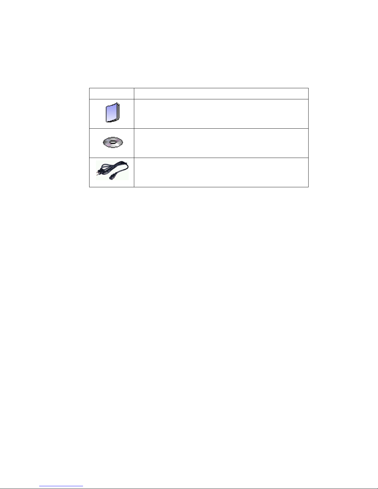
Check the box contents!
Item Name
1 x WinFast WS1000 Quick Installation Guide
1 x WinFast WS1000 Driver CD
1 x WinFast WS1000 Power Cord
IMPORTANT NOTE:
If any of these items are missing, please contact your vendor/dealer for
replacement before continuing with the installation process.
Page 5

5
Chapter 1: Instruction
1.1 - Congratulations
You have purchased the powerful WinFast WS1000 workstation, based on the
Intel® Patsburg-A (PCH). The WinFast WS1000 is designed to support dual
Intel®Xeon E5-2600 (LGA2011) Series Processors and up to 512GB LR-DIMM (800,
1066 and 1333MHz), 256GB R-DIMM (800, 1066, 1333 and 1600MHz) DDR3
memory modules. Leveraging advanced technology from Intel®, the WinFast
WS1000 is capable of offering scalable 32 and 64-bit computing, high-bandwidth
memory design, and lightning-fast PCI-E bus implementation.
The WinFast WS1000 not only empowers you in today’s demanding IT
environment but also offers a smooth path for future application upgradeability.
All of these rich feature sets provides the WinFast WS1000 with the power and
flexibility to meet demanding requirements for today’s IT environments.
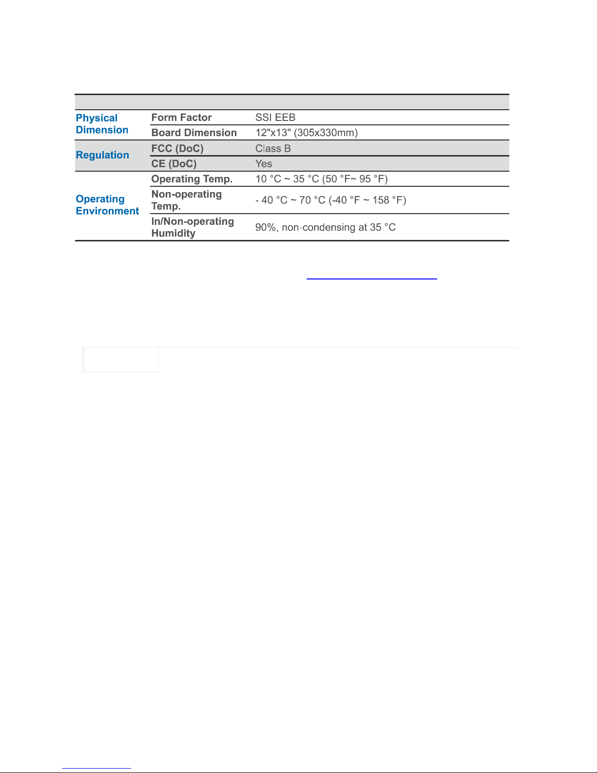
1.2 - Hardware Specifications
WinFast WS1000
Supported CPU
Series
Intel Xeon Processor E5-2600 Series
Socket Type / Q'ty
(2) LGA2011
Thermal Design
Power (TDP)
wattage
Max up to 150W
Processor
System Bus
Up to 8.0/ 7.2/ 6.4 GT/s with Intel QuickPath
Interconnect (QPI) support
PCH
Intel C602
Super I/O
NCT5577D
Chipset
PCI-E Switch
Pericom PI3PCIE3412
Supported DIMM
Qty
(8)+(8) DIMM slots
DIMM Type / Speed
DDR3/DDR3L 800 / 1066 / 1333 / 1600 RDIMM, 800 /
1066 / 1333 UDIMM / LRDIMM / Support DDR3
Unbuffered and Register ECC
Capacity
up to 128GB UDIMM / 256GB RDIMM / 512GB
LRDIMM
Memory channel
4 Channels per CPU
Memory
Memory voltage
1.5V or 1.35V
Page 6

6
Expansion
Slots
PCI-E
(1) PCI-E x4 slot ( x4 link, slot #6)
(1) PCI-E x16 slot ( x16 link or x8 link, slot #5)
(1) PCI-E x8 slot ( x0 link or x8 link, slot #4)
(1) PCI-E x16 slot ( x16 link or x8 link, slot #3)
(1) PCI-E x8 slot ( x0 link or x8 link, slot #2)
(1) PCI-E x8 slot (w/ x4 link PCH), slot #1
Port Q'ty
(2) GbE ports
LAN
Controller
Intel 82574L
Connector
(10) SATA
Controller
Intel C602
Speed
(2)6.0Gb/s BLUE ; (4)3.0Gb/s black ; (4)3.0Gb/s
1BLUE+3BLACK
Storage SATA
RAID
RAID 0/1/10/5 (Intel RST)
Chipset
Realtek ALC892-GR
Audio
Feature
HDA7.1+2channel
Port Q'ty
(2)1394 ports
FireWire
Chipset
VIA VT6315
USB
(7) USB2.0 ports (2 at rear, 4 via cable, 1 type A
onboard) / (4) USB3.0 ports (4 at rear)
COM
(1) port (at rear)
Audio
(1) 2x5-pin front panel audio header
(line out and Mic in)
(1) Line-in, (1)Line-out, (1)Mic-in, (1)Surround, (1)Side
surround, (1)CEN/LFE at rear
S/PDIF In
(1) Coaxial SPDIF In
S/PDIF Out
(1) Optical SPDIF out
RJ-45
(2) GbE ports
Power
(1) ATX24-pin + (1)8-pin +
(1)8-pin power connectors
/(1) 4-pin power connector for PCI-E SLOT
PSMI
(1) 1x5-pin header
SGPIO
(1) SATA SGPIO header
(2) SAS SGPIO header
Front Panel Header
(1) 2x12-pin FPB header
Input /Output
SATA
(8) SATA-II and (2) SATA-III connectors
Chipset
Winbond W83795G
Voltage
Monitors voltage for CPU, memory, chipset & power
supply
Fan
Total (7) 4-pin headers / (1)10x2-pin fan header
System
Monitoring
Temperature
Monitors temperature for CPU & system environment
Brand / ROM size
AMI / 8MB
BIOS
Feature
Plug and Play (PnP) /PCI2.3 /WfM2.0 /SMBIOS2.3
/PXE boot / ACPI 2.0 power management /Power on
mode after power recovery / User-configurable H/W
monitoring / Auto-configurable of hard disk types
Page 7
7
Remember to visit Leadtek’s Website at http://www.leadtek.com. There you
can find information on all products with FAQs, online manuals and BIOS
upgrades and more.
Page 8
8
Chapter 2: Board Installation
You are now ready to install your motherboard.
How to install our products right… the first time
The first thing you should do is reading this user’s manual. It contains important
information that will make configuration and setup much easier. Here are some
precautions you should take when installing your motherboard:
(1) Ground yourself properly before removing your motherboard from the antistatic
bag. Unplug the power from your computer power supply and then touch a
safely grounded object to release static charge (i.e. power supply case). For
the safest conditions, we recommend wearing a static safety wrist strap.
(2) Hold the motherboard by its edges and do not touch the bottom of the board, or
flex the board in any way.
(3) Avoid touching the motherboard components, IC chips, connectors, memory
modules, and leads.
(4) Place the motherboard on a grounded antistatic surface or on the antistatic bag
that the board was shipped in.
(5) Inspect the board for damage.
The following pages include details on how to install your motherboard into your
chassis, as well as installing the processor, memory, disk drives and cables.
Caution!
1. To avoid damaging the motherboard and associated
components, do not use torque force greater than
7kgf/cm (6.09 lb/in) on each mounting screw for
motherboard installation.
2. Do not apply power to the board if it has been
damaged.
Page 9
9
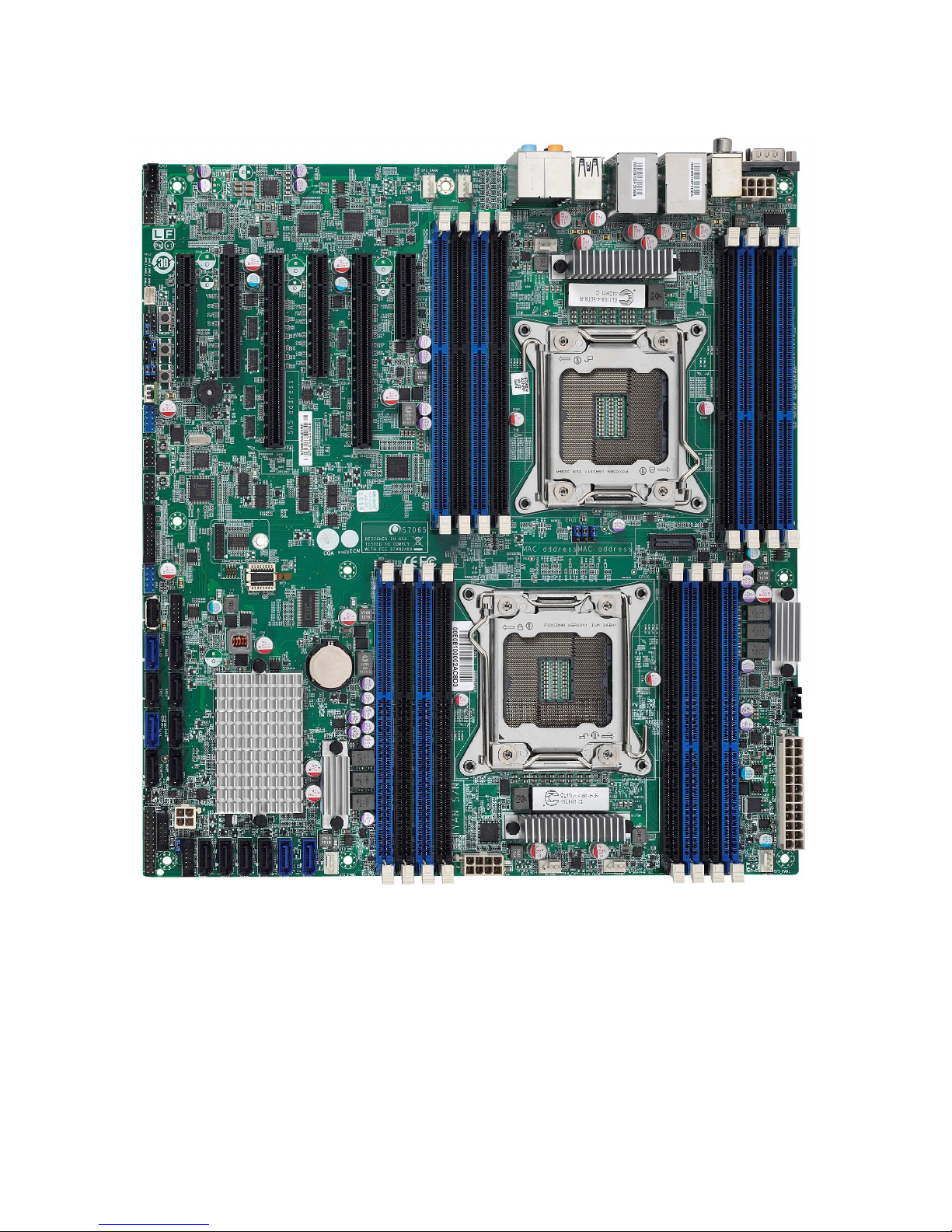
2.1 - Board Image
WinFast WS1000
This diagram is representative of the latest motherboard revision available at the time
of publishing. The board you receive may not look exactly like the above diagram.
Page 10
10
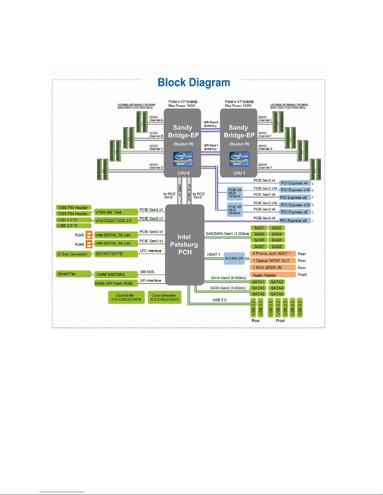
2.2 - Block Diagram
WinFast WS1000 Block Diagram
Page 11
11
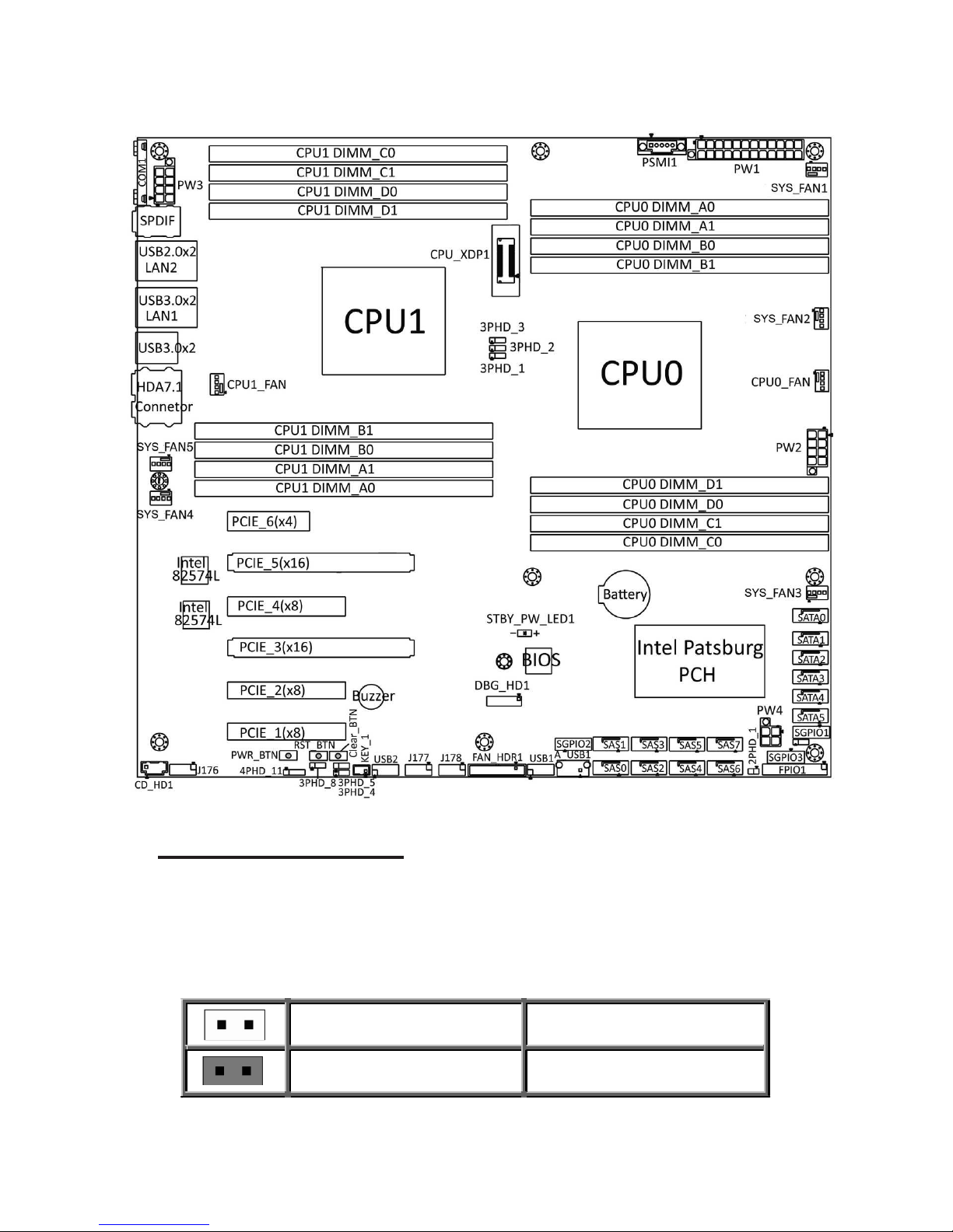
2.3 - Board Parts, Jumpers and Connectors
Important Notes to the User
• "▲" indicates the location of "Pin 1".
• The diagram is representative of the latest board revision available at the time of
publishing. The board you received may not look exactly
like this
diagram.
Jumper Legend
OPEN - Jumper OFF Without jumper cover
CLOSED - Jumper ON With jumper cover
Page 12

12
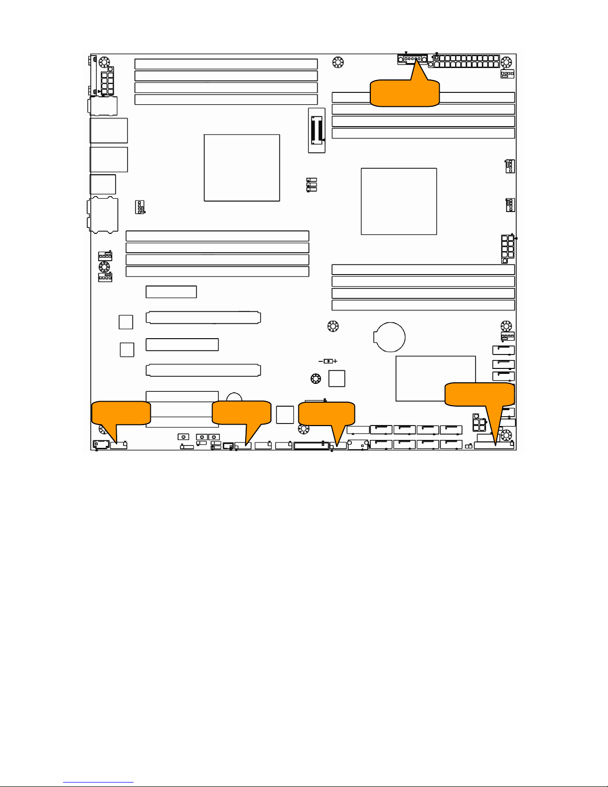
Jumpers & Connectors
Jumper/Connector
Function
SYS FAN1~5
4-pin Fan Power Connector
CPU0~1FAN
4-pin CPU0/CPU1 Fan Power Connector
FAN_HDR1
System Fan Header
SPDIF
Coaxial-Input(upper) / Optical-Output(lower)
J176
Front Panel Audio
J177/J178
1394 Pin Header
SGPIO1
SATA 0~5 SGPIO Header
SGPIO2
SAS 0~3 SGPIO Header
SGPIO3
SAS 4~7 SGPIO Header
CD_HD1
CD Input Header
PSIMI1
PSMI Connector
FPIO_1
Front Panel Header
FAN_HDR1
Fan Connector for Barebone
A_USB1
TYPE-A USB From PCH
USB1/ USB2
Front USB Header
KEY1
Patsburg Upgrade ROM Header
Reset BTN
Reset Button
Clear BTN
RTC reset Button
2PHD_1
Intruder Header
3PHD_1/2/3
CPU XDP Bypass Jumper
3PHD_4
ME Recovery Mode Jumper
3PHD_5
BIOS Recovery Mode Jumper
3PHD_8
Security Override Jumper
4PHD_11
BUZZER disable Jumper
DBG_HD1
WinFast Module Header
SATA0/SATA1
SATA3.0 Connector
SATA2/SATA5
SATA2.0 Connector
SAS0~7
PCH SAS Connector
Page 13
13
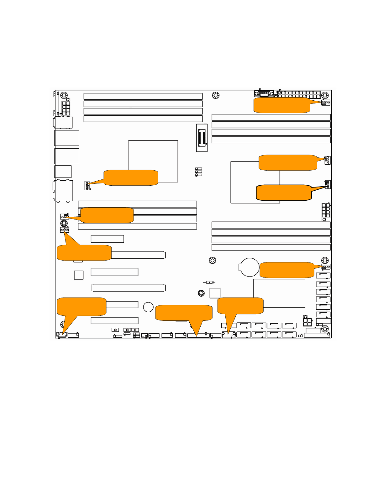
Jumper Placement
SYS_FAN1
CPU1_FAN
SYS_FAN2
CPU0_FAN
SYS_FAN5
SYS_FAN4
SYS_FAN3
CD_HD1 A_USB1
FAN_HDR1
Page 14
14
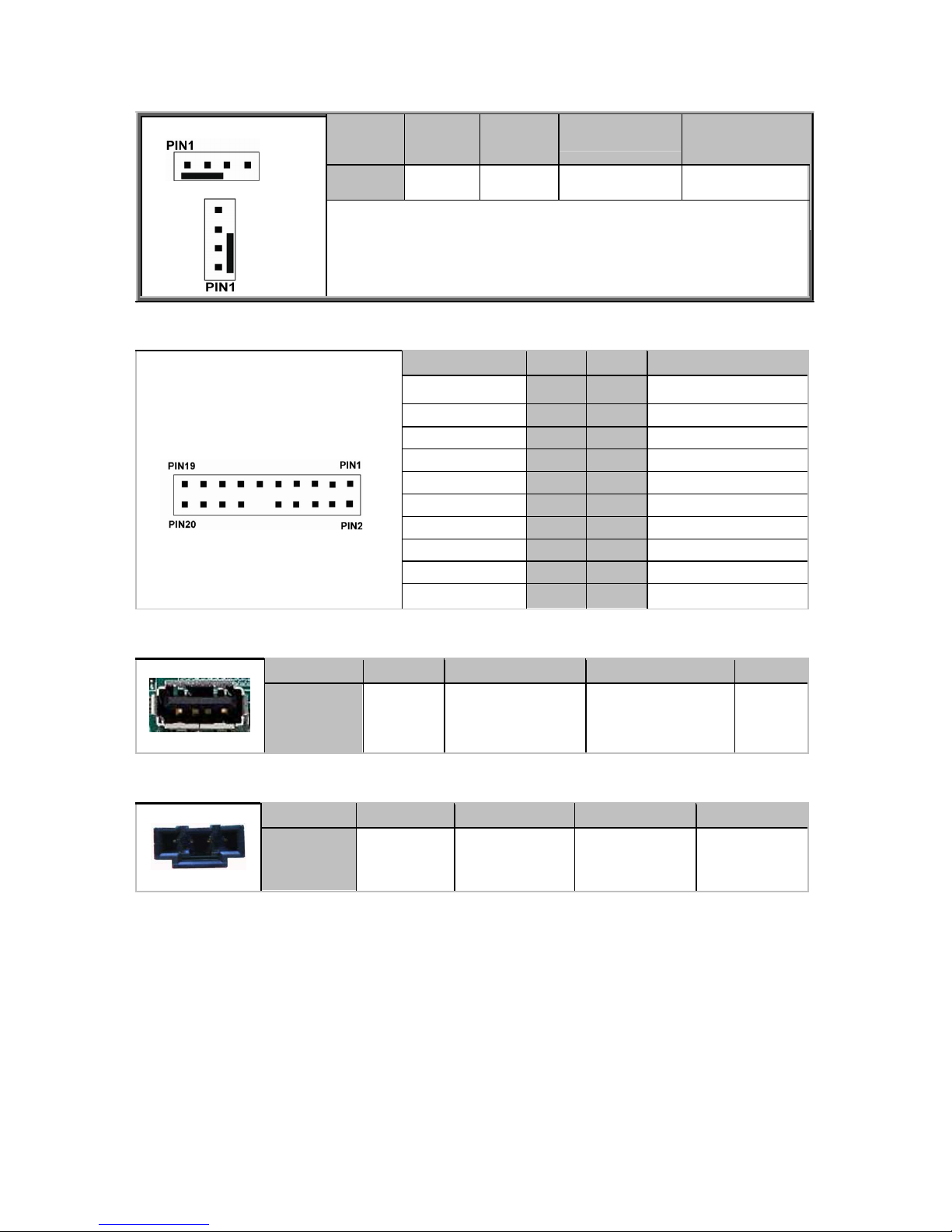
Pin
1
2
3
4
Signal
GND
P12V
FAN_TACH
FAN_PWM
NOTE:
SYS FAN1~5/CPU0~1FAN: 4-Pin FAN Connector
Use this header to connect the cooling fan to your motherboard
to keep the system stable and reliable
.
FAN_HDR1: FAN Connector for Barebone
Signal Pin Pin Signal
TACH1
1
2
TACH6
TACH2
3
4
TACH7
TACH3
5 6
TACH8
TACH4
7
8
TACH9
TACH5
9
10
TACH10
GND
11
12
KEY
PWM2
13
14
PWM1
TACH11
15
16
SDA
TACH12
17 18
SCL
VCC3_AUX
19
20
PWM3
A_USB1: Vertical TYPE-A USB From PCH
Pin 1 2 3 4
Signal
+5V
USB DATA2-
USB DATA2+
GND
CD_HD1: CD Input Header
Pin 1 2 3 4
Signal
CD_IN_L
GND
GND
CD_IN_R
Page 15
15
PSMI1
J176
USB2
USB1
FPIO1
Page 16
16
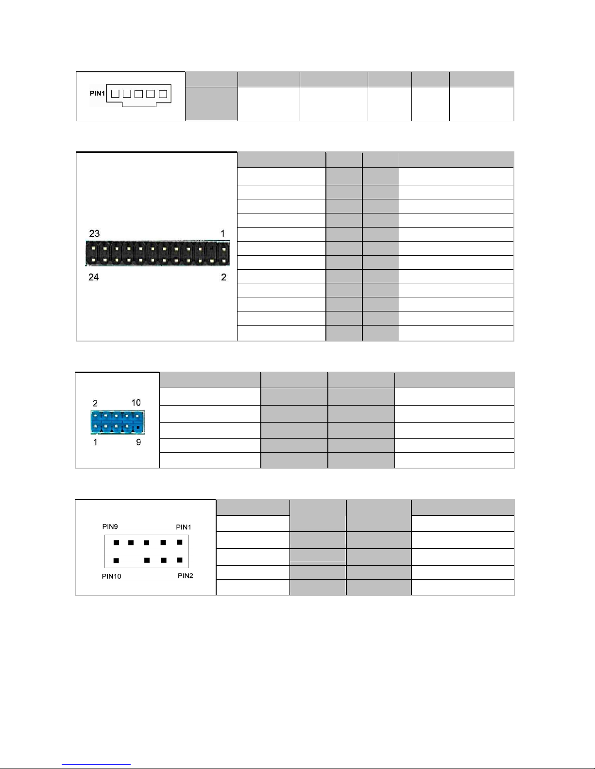
PSMI1: PSMI Connector
Pin 1 2 3 4 5
Signal
SMB_CLK
SMB_DAT
PSU
Alert#
GND
VCC3
FPIO_1: Front Panel Header
Signal
Pin Pin Signal
PWRLED+
1
2
FPPW (VCC3_AUX)
KEY
3
4
NA
PWRLED-
5
6
NA
HD_LED+
7
8
HWM_FAULT_LED-
HD_LED-
9
10
SYS_FAULT_LED-
PWR_SW#
11
12
LAN1_ACTIVE_LED+
GND
13
14
LAN1_ACTIVE_LED-
RST_SW#
15 16
SDA
GND
17
18
SCL
NA
19
20
INTRUDER#
FPIO_TEMP_IN
21
22
LAN2_ACTIVE_LED+
NMI_SW#
23
24
LAN2_ACTIVE_LED-
USB1/USB2: Front USB Header
Signal Pin Pin Signal
VCC
1
2
VCC
USB DATA1-
3
4
USB DATA2-
USBDATA1+
5
6
USB DATA2+
GND
7
8
GND
KEY
9
10
NC
J176: Front Panel Audio
Signal Pin Pin Signal
MIC2-L
1
2
GND
MIC2-R
3
4
FP_Present
LINE2-R
5
6
MIC2-JD
GND
7
8
Key
LINE2_L
9
10
LINE2-JD
Page 17
17
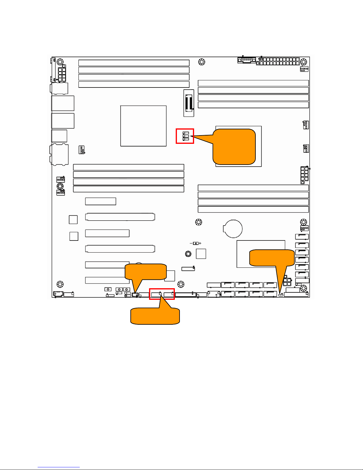
3PHD_3
3PHD_2
3PHD_1
KEY_1
2PHD_1
J177/J178
Page 18
18
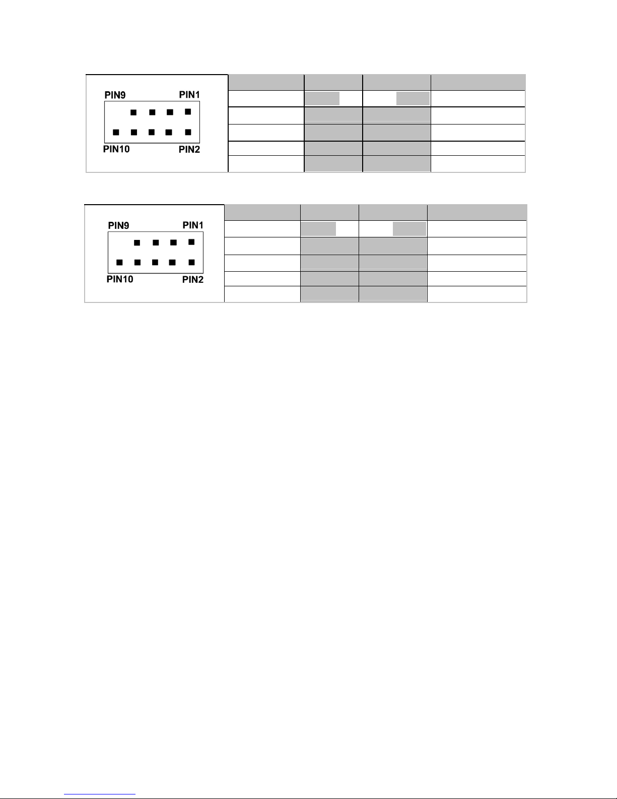
J177: 1394 Pin Header
Signal Pin Pin Signal
XTP_A_P_0
1
2
XTP_A_N_0
GND
3
4
GND
XTP_B_P_0
5
6
XTP_B_N_0
VCC12_1394
7
8
VCC12_1394
KEY
9
10
GND
J178: 1394 Pin Header
Signal Pin Pin Signal
XTP_A_P_1
1
2
XTP_A_N_1
GND
3
4
GND
XTP_B_P_1
5
6
XTP_B_N_1
VCC12_1394
7
8
VCC12_1394
KEY
9
10
GND
Page 19
19
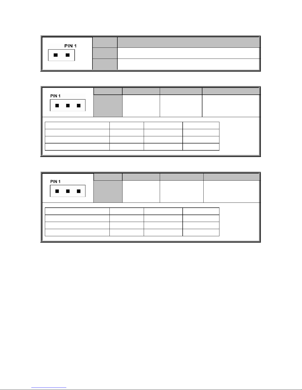
2PHD_1: INTRUDER Header
Pin Signal
1
PCH_INTRUDER_N
2
GND
3PHD_1 / 3PHD_2: CPU XDP bypass Jumper
Pin 1 2 3
Signal
CPU0_TDO
XDP_TDO
CPU1_TDO
Default: Only CPU0
3PHD_1
3PHD_2
3PHD_3
Only CPU0 Installed
1-2
1-2
1-2
Only CPU1 Installed
2-3
2-3
1-2
Both CPU Installed
1-2
2-3
2-3
3PHD_3: CPU XDP bypass Jumper
Pin 1 2 3
Signal
NC
CPU0_TDO
CPU1_TDI
Default: Only CPU0
3PHD_1
3PHD_2
3PHD_3
Only CPU0 Installed
1-2
1-2
1-2
Only CPU1 Installed
2-3
2-3
1-2
Both CPU Installed
1-2
2-3
2-3
Page 20
20
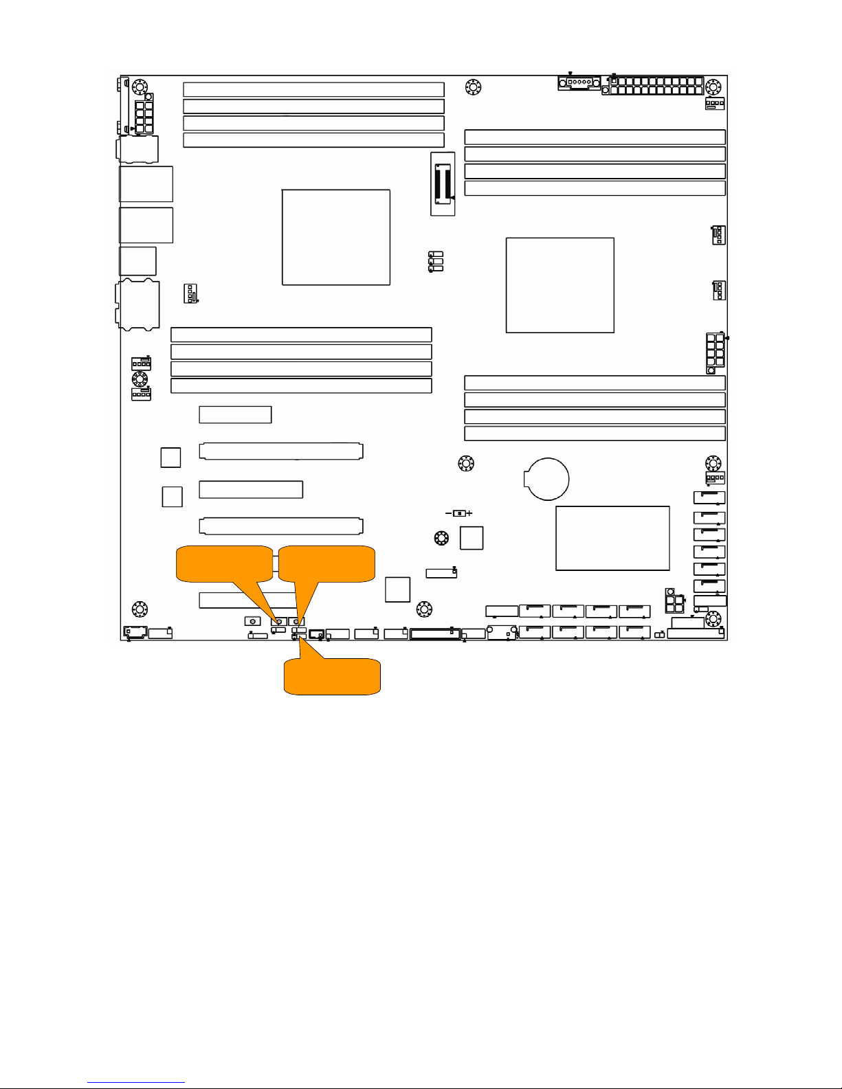
3PHD_8 3PHD_5
3PHD_4
Page 21
21
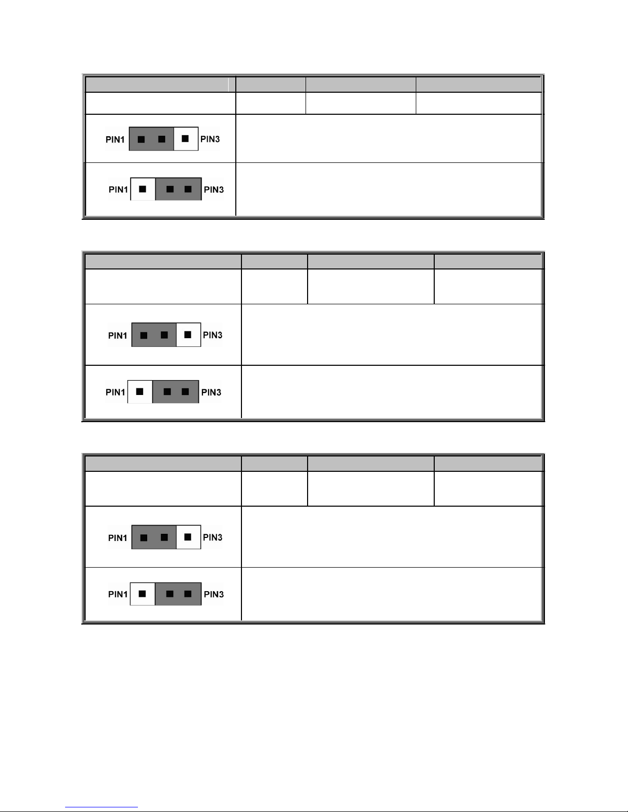
3PHD_4: ME RECOVERY MODE Jumper
Pin
1
2
3
Signal
NC
FM_ME_RCVR_N GND
1-2: Normal Mode (Default)
2-3: ME Recovery Mode
3PHD_5: BIOS RECOVERY Jumper
Pin 1 2 3
Signal
NC BIOS_RCVR_BOOT_N GND
1-2: Normal Mode (Default)
2-3: BIOS Recovery mode
3PHD_8: SECURITY OVERRIDE Jumper
Pin 1 2 3
Signal
NC MFG_MODE_N GND
1-2: Normal Mode (Default)
2-3: Security Override
Page 22
22
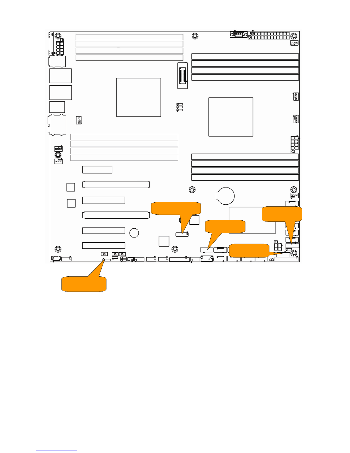
DBG
HD1
SGPIO2
SGPIO1
SGPIO3
4PHD_11
Page 23
23
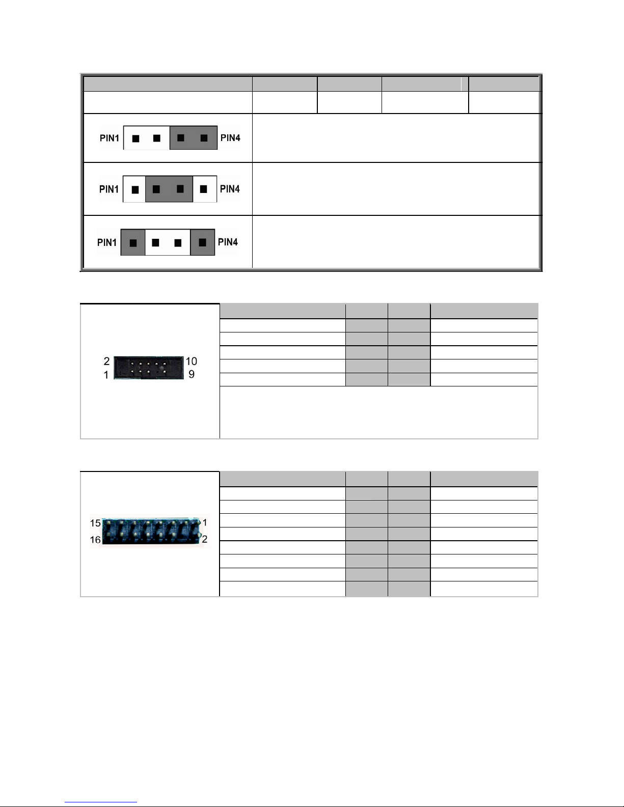
4PHD_11: BUZZER disable Jumper
Pin 1 2 3 4
Signal
VCC5
NA
BUZ_1
BUZ_2
1-2: Normal Mode (Default)
2-3: Disable PC Beep
1-4: Use the external speaker
SGPIO1/2/3: SATA SGPIO Header
Signal
Pin Pin Signal
SCL
1
2
SDATA IN
SDA
3
4
SDATA OUT-
GND
5
6
SLOAD
KEY
7
8
SCLOCK
P3V3_AUX
9
10
HD_ERROR_LED
NOTE:
SGPIO1 is responsible for
SATA port 0~5
SGPIO2 is responsible for
SAS 0~3
SGPIO3 is responsible for
SAS 4~7
DBG_HD1: WinFast Module Header
Signal
Pin Pin Signal
P3V3
1
2
FRAME_N
LAD0
3
4
KEY
LAD1
5
6
PLT_RST_N
LAD2
7
8
GND
LAD3
9
10
CLK_33M
DBG_SERIRQ
11
12
GND
DBG_PRES_N
13
14
VCC3_AUX
ADDR_MB
15
16
PCH_PP_EN
Page 24
24
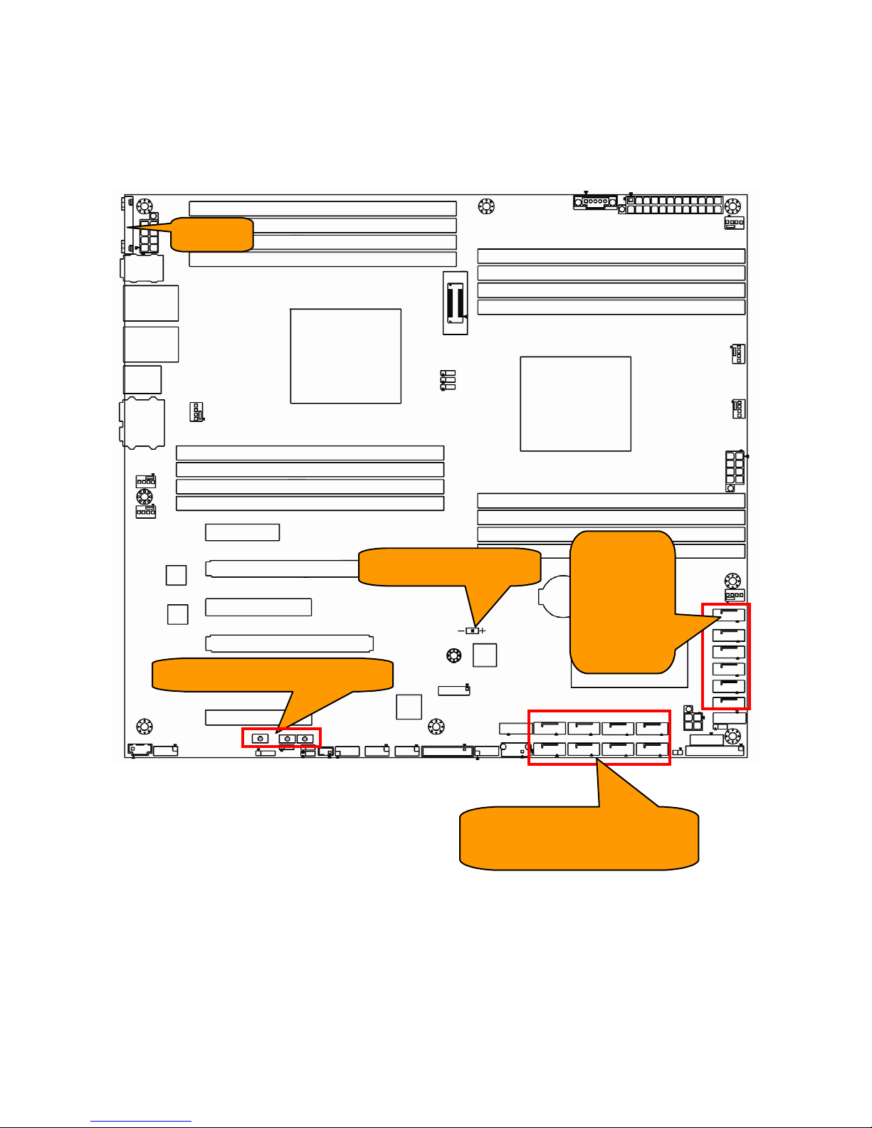
COM1
PWR/RST/Clear Button
STBY_PW_LED1
SATA0
SATA1
SATA2
SATA3
SATA4
SATA5
These connectors have no
functions. Do not connect
hard drives to them.
Page 25
25
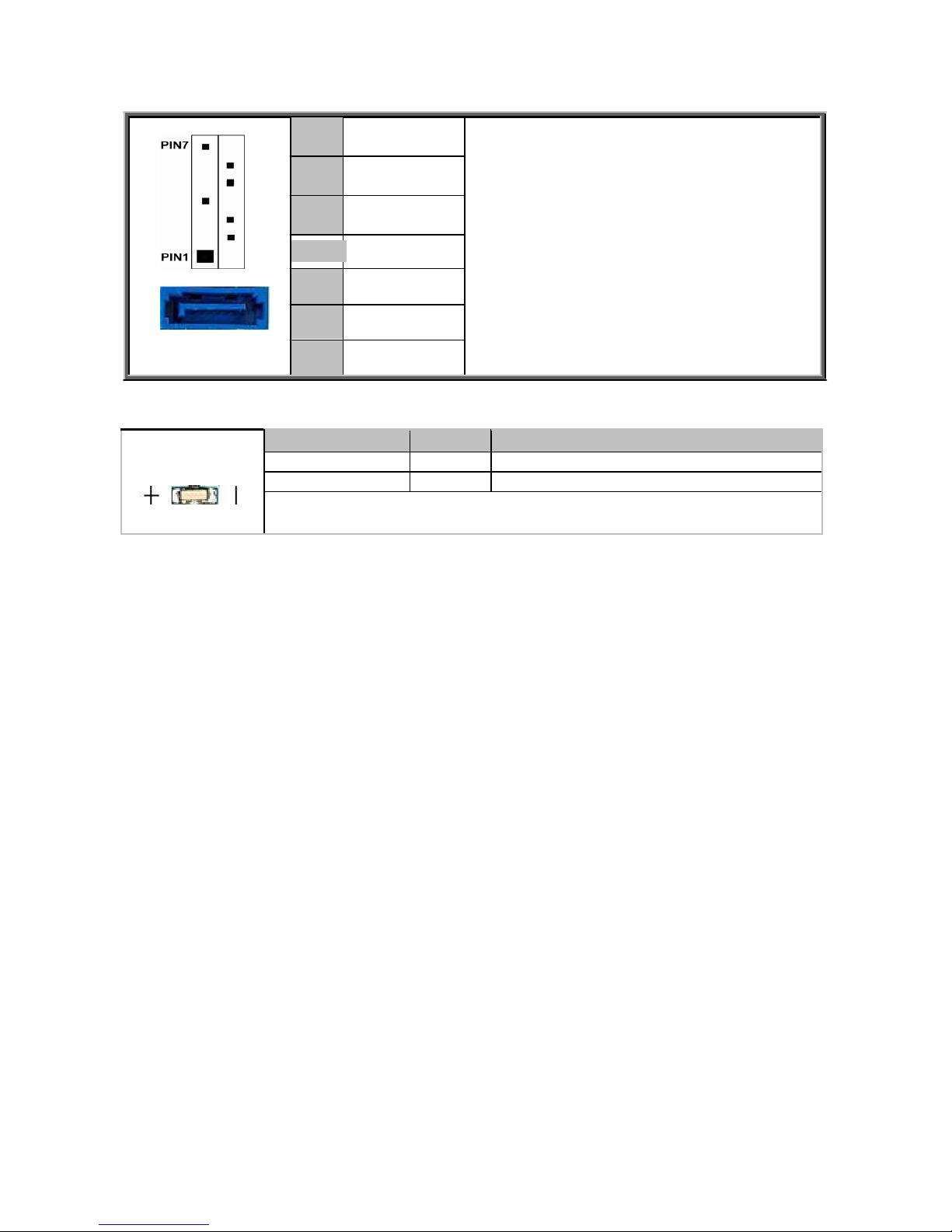
SATA0/SATA1/SATA2/SATA3/SATA4/SATA5: SATA Connector
PIN7 PIN1
7
GND
6
SATA RX DP
5
SATA RX DN
4
GND
3
SATA TX DN
2
SATA TX DP
1
GND
Connects to the Serial ATA ready drives via
the Serial ATA cable.
SATA0/SATA1:
Support SATA3.0
SATA2/SATA3/SATA4/SATA5:
Support SATA2.0
SYTB_PW_LED1: Stby_PW_LED
State
Color
Descri
p
tion
On
Green
System standby power identified
Off
Off
System standby power not identified
NOTE: The STBY_PW_LED will always be Green when attached with
AC cable.
Page 26
26
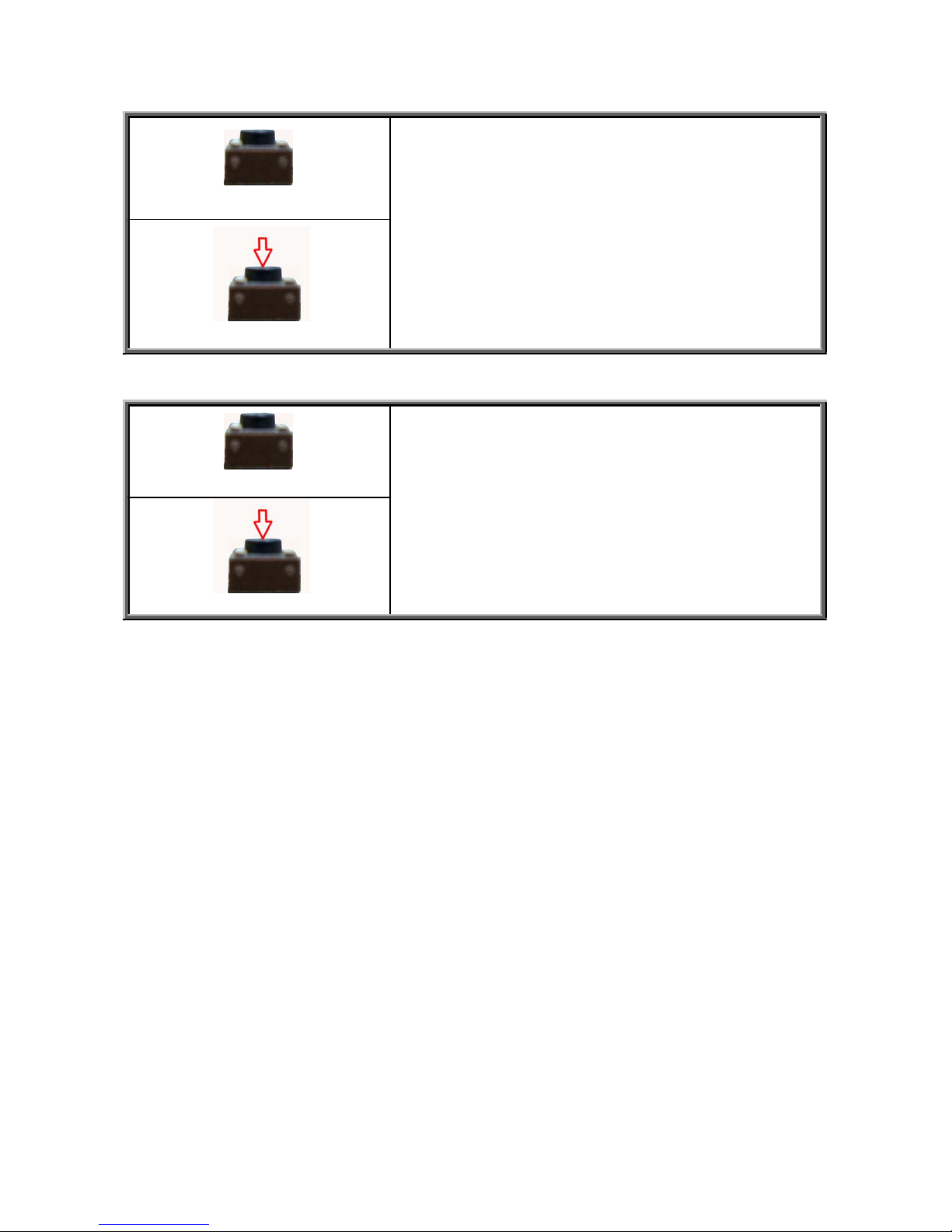
CLEAR BUTTON : Clear CMOS set
Normal(Default)
Clear CMOS
You can reset the CMOS settings by using this button if
you have forgotten your system/setup password or
need to clear system BIOS setting
.
-
1.Power off system and disconnect power
connectors from the motherboard
-
2.Press the button (Clear CMOS)
-
3.Reconnect power & power on system
NOTE:
After flashing new BIOS please follow the
steps:
a. Clear CMOS
b. Enter BIOS setup menu and load Default
Settings.
Then do a Save and Exit from setup.
RST BUTTON : Reset system set
Normal (Default)
Press the button to reset the system
.
Reset system
Page 27
27
2.4 - Installing the Processor
Your brand new WinFast WS1000 motherboard supports both Intel® “Sandy
Bridge-EP and Ivy Bridge series” processors.
NOTE: Leadtek is not liable for damage as a result of operating an unsupported
configuration.
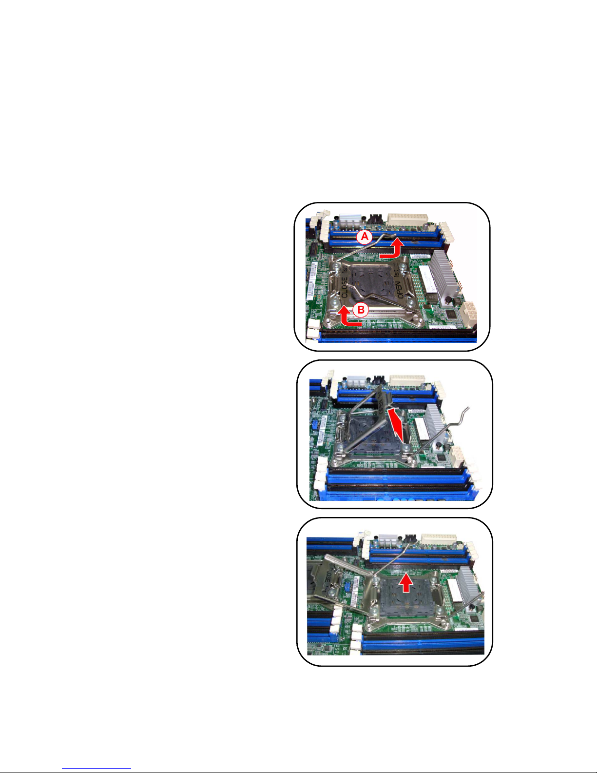
Locate the CPU socket (LGA 2011) on the motherboard:
To install a CPU:
1. Press the load lever (A) hard
with your thumb first, move it to
the right. Then press the load
lever(B) and move it to the right
side until the load plate is
released from the retention tab.
2. Lift the load plate in the
direction of the arrow until it is
fully opened.
3. Remove the PnP cap from the
CPU socket.
Page 28
28
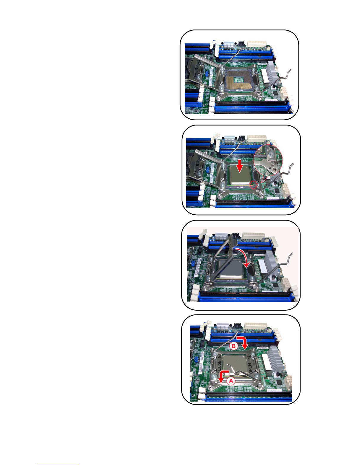
4. Please refer to the image.
5. Position the CPU over the
socket, ensuring that the gold
triangle is on the bottom-right
corner of the socket, and then
fit the socket alignment keys
into the CPU notches.
6. Close the load plate, ensuring
that the front edge of the load
plate slides under the retention
lever.
7. Insert the load lever under the
retention tab.
Page 29
29
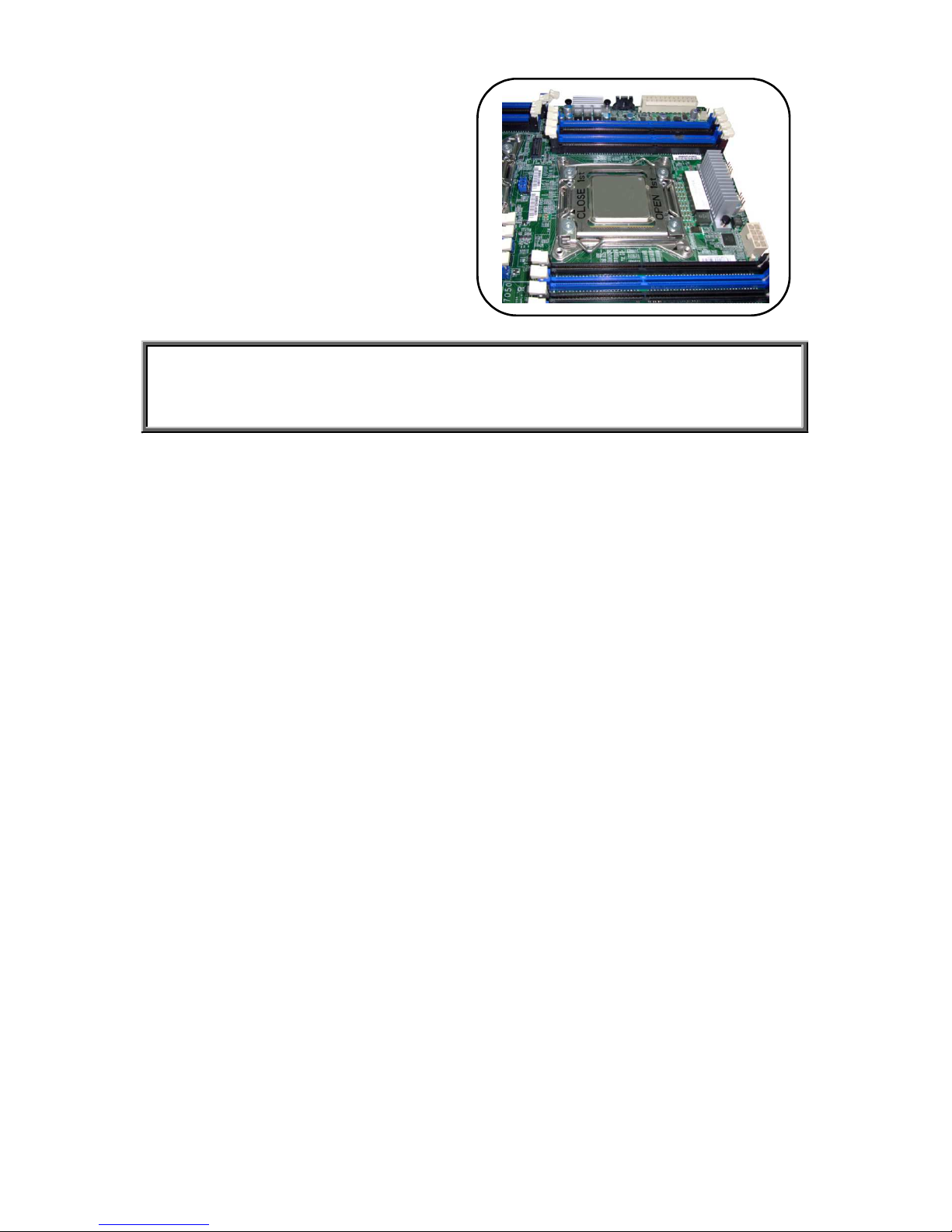
Cautions: The CPU fits in only one correct orientation. Do not force the CPU
into the socket to prevent bending the connectors on the socket and
damaging the CPU.
Page 30
30
2.5 - Installing the Heatsink
Heatsink Installation
Caution: After installing the processor, you should proceed to install the heat sink.
The CPU heat sink will ensure that the processor do not overheat and continue to
operate at maximum performance for as long as you own them. The overheated
processor is dangerous to the motherboard.
For the safest method of installation and information on choosing the appropriate
heat sink, using heat sinks validated by Intel®. Please go to Intel’®s website at
www.Intel.com.
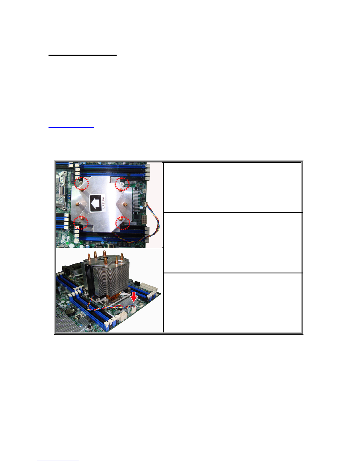
The following diagram illustrates how to install heat sink onto the CPU of WinFast
WS1000.
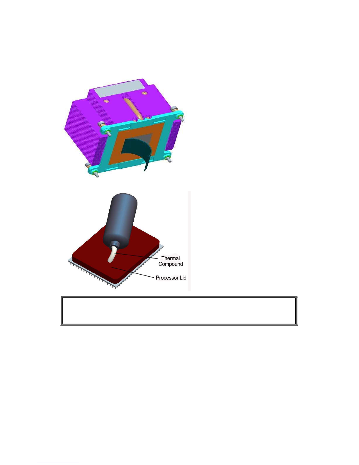
1. If a protective film covers the thermal
interface material (TIM) on the underside
of the heatsink, remove the protective
film.
2. Each heatsink has four captive
fasteners and should be tightened as
shown
3. Attach fan power cable to server board
as shown.
Page 31
31
2.6 - Thermal Interface Material
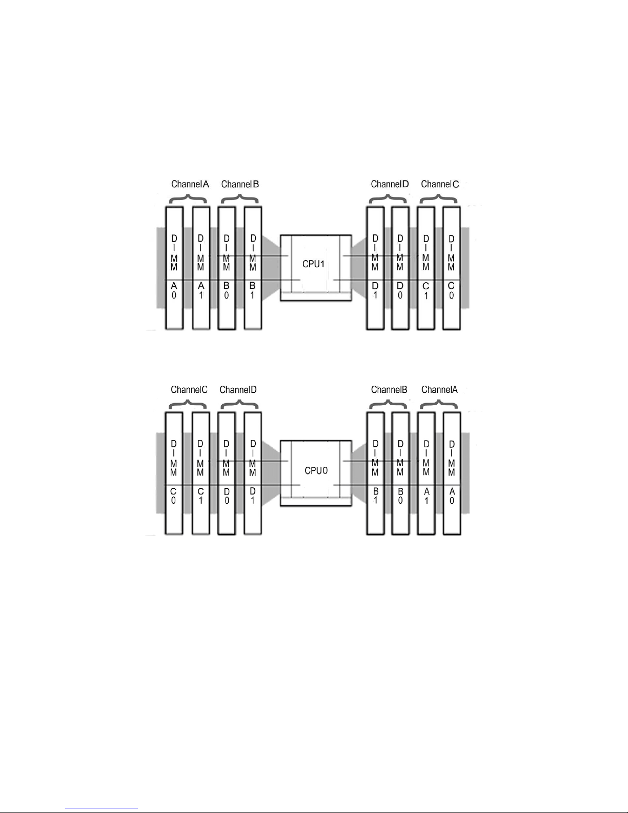
There are two types of thermal interface materials designed for use with the
processors.
The most common material
comes as a small pad
attached to the heat sink at
the time of purchase. There
should be a protective cover
over the material. Take care
not to touch this material.
Simply remove the protective
cover and place the heat sink
on the processor.
The second type of interface
material is usually packaged
separately. It is commonly
referred to as ‘thermal
compound’. Simply apply a
thin layer on to the CPU lid
(applying too much will
actually reduce the cooling).
NOTE: Always check with the manufacturer of the heat sink & processor
to ensure the thermal Interface material is compatible with the processor
and meets the manufacturer’s warranty requirements.
Page 32
32
2.7 - Installing the Memory
Overview
The motherboard comes with four Double Data Rate 3(DDR3)Dual Inline
Memory Modules (DIMM)sockets.
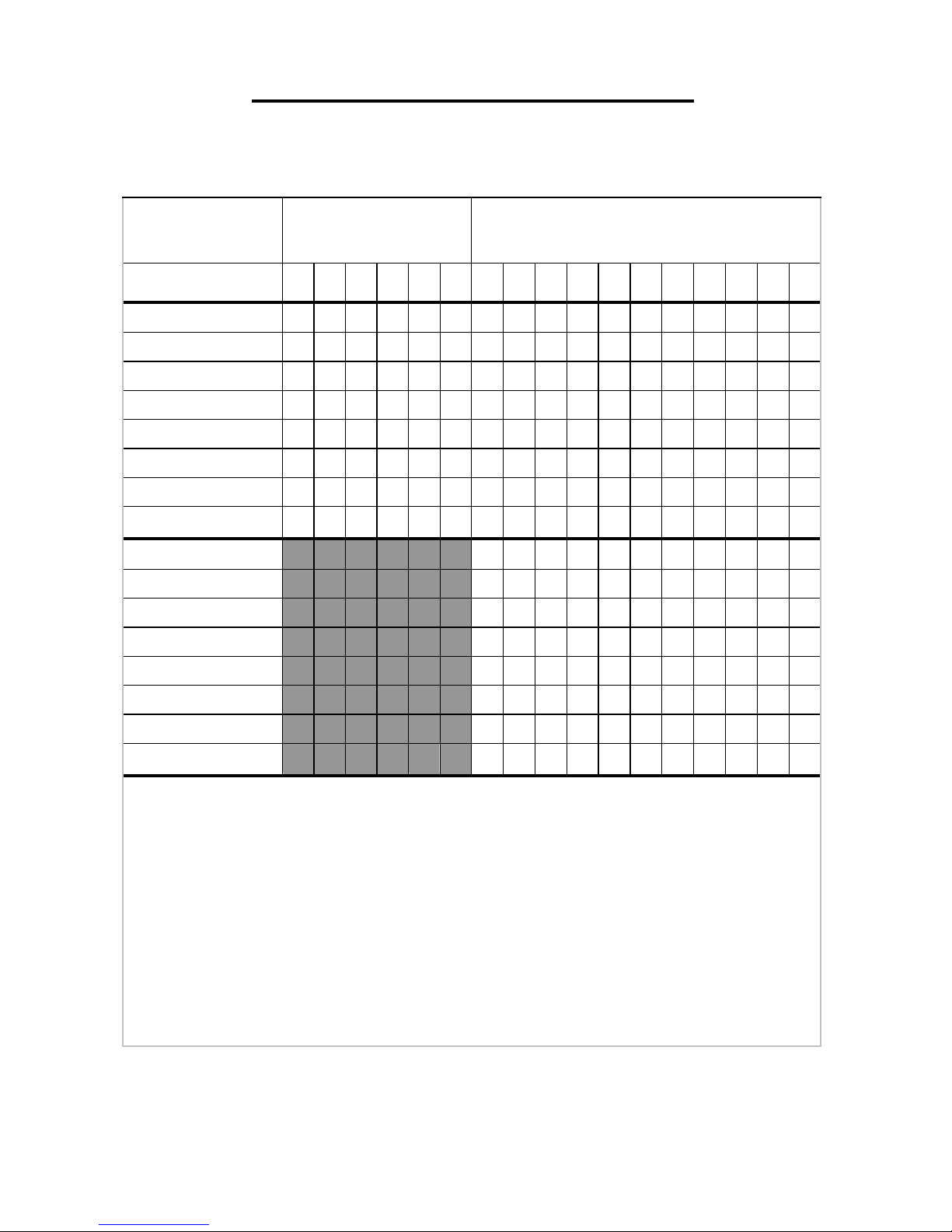
The figure illustrates the location of the DDR3 DIMM socket.
• Sandy Bridge-EP/EX processor supports 4 DDR3 channels
• Unbuffered DDR3 and registered DDR3 DIMMs
• LR DIMM (Load Reduced DIMM) for buffered memory solutions demanding
higher capacity memory subsystems
• Memory DDR3 data transfer rates of 800, 1066, 1333, and 1600 MT/s
• All installed memory will automatically be detected and no jumpers or settings
need changing.
• All memory must be of the same type and density.
• Always populate the memory starting from DIMMA0 first.
Page 33
33
Recommended Memory Population Table
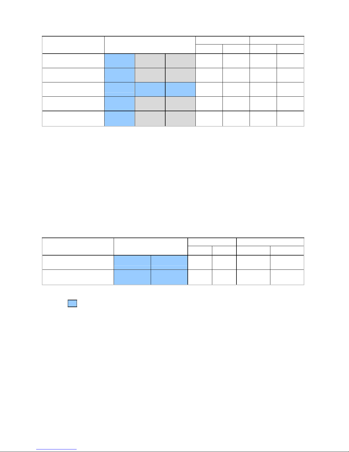
To achieve the best performance, Leadtek strongly recommend memory installation
configuration as listed below:
Single CPU
Installed
(CPU0 only)
Dual CPU
installed
(CPU0 and CPU1)
Quantity of
memory installed
1 2 3 4 6 8 2 3 4 5 6 7 8 10 12 14 16
CPU0_DIMMD0
√ √ √
√ √ √ √ √ √
CPU0_DIMMD1
√
√ √ √
CPU0_DIMMC0
√ √ √ √
√ √ √ √ √ √ √ √
CPU0_DIMMC1
√
√ √ √
CPU0_DIMMB0
√ √ √ √ √
√ √ √ √ √ √ √ √ √ √
CPU0_DIMMB1
√ √
√ √ √ √
CPU0_DIMMA0
√ √ √ √ √ √ √ √ √ √ √ √ √ √ √ √ √
CPU0_DIMMA1
√ √
√ √ √ √
CPU1_DIMMD0
√ √ √ √ √
CPU1_DIMMD1
√
CPU1_DIMMC0
√ √ √ √ √ √ √
CPU1_DIMMC1
√
CPU1_DIMMB0
√ √ √ √ √ √ √ √ √
CPU1_DIMMB1
√ √
CPU1_DIMMA0
√ √ √ √ √ √ √ √ √ √ √
CPU1_DIMMA1
√ √
1. √ indicates a populated DIMM slot.
2. Paired memory installation for Max performance.
3. Populate the same DIMM type in each channel, specifically
- Use the same DIMM size
- Use the same # of ranks per DIMM
4. Dual-rank DIMMs are recommended over single-rank DIMMs
5. Un-buffered DIMM can offer slightly better performance than registered DIMM if populating only a
single DIMM per channel
6. We don't suggest other memory installation
Page 34
34
Intel®Xeon®processor E5-2600/4600 product families UDIMM Support
1.35V
1.50V
Ranks Per DIMM &
Data Width
Memory Capacity per DIMM
1DPC 2DPC 1DPC 2DPC
SRx8 Non-ECC
1 GB
2GB
4GB
N/A
N/A
1066,
1333
1066,
1333
DRx8 Non-ECC
2GB
4GB
8GB
N/A
N/A
1066,
1333
1066,
1333
SRx16 Non-ECC
512 MB
1GB
2GB
N/A
N/A
1066,
1333
1066,
1333
SRx8 ECC
1GB
2GB
4GB
1066
1066
1066,
1333
1066,
1333
DRx8 ECC
2GB
4GB
8GB
1066
1066
1066,
1333
1066,
1333
NOTE 1: The blue blocks indicate that the DRAM Densities are supported but not validated.
NOTE 2: The grey blocks indicate that the DRAM Densities are supported and validated.
NOTE 3: 1DPC => One dimm per channel
NOTE 4: 2DPC => Two dimm per channel
Supported DRAM Densities are 1Gb, 2Gb and 4Gb. Only 2Gb and 4Gb are validated by
Intel.
Command Address Timing is 1N for 1DPC and 2N for 2DPC.
Romley-EP/EX platform does not support 3DPC when using UDIMMs.
Intel®Xeon®processor E5-2600/4600 product families LRDIMM Support
1.35V
1.50V
Ranks Per DIMM &
Data Width
Memory Capacity per
DIMM
1DPC 2DPC
1DPC
2DPC
QRx4 (DDP)
16GB
32GB
1066 1066
1066,
1333
1066,
1333
QRx8 (P)
8GB
16GB
1066 1066
1066,
1333
1066,
1333
NOTE:
The blue blocks indicate that the DRAM Densities are supported and not validated.
Physical Rank is used to calculate DIMM Capacity
.
Supported and validated DRAM Densities are 2Gb and 4Gb.
Command Address Timing is 1N.
The speeds are estimated targets and will be verified through simulation.
For 3SPC/3DPC -Rank Multiplication (RM) >= 2.
DDP -Dual Die Package DRAM stacking. P –Planer monolithic DRAM Die.
Romley-EP/EX platform does not support 3DPC when using E5-2400 LRDIMMs.
Page 35
35
Intel®Xeon®processor E5-2600/4600 product families RDIMM Support
1.35V
1.50V
Ranks
Per
DIMM &
Data
Width
Memory Capacity per
DIMM
1DPC
2DPC
1DPC
2DPC
SRx8
1GB
2GB
4GB
1066,
1333
1066,
1333
1066,
1333,
1600
1066,
1333,
1600
DRx8
2GB
4GB
8GB
1066,
1333
1066,
1333
1066,
1333,
1600
1066,
1333,
1600
SRx4
2GB
4GB
8GB
1066,
1333
1066,
1333
1066,
1333,
1600
1066,
1333,
1600
DRx4
4GB
8GB
16GB
1066,
1333
1066,
1333
1066,
1333,
1600
1066,
1333,
1600
QRx4
8GB 16GB 32GB 800
800
1066
800
QRx8
4GB 8GB
16GB 800
800
1066
800
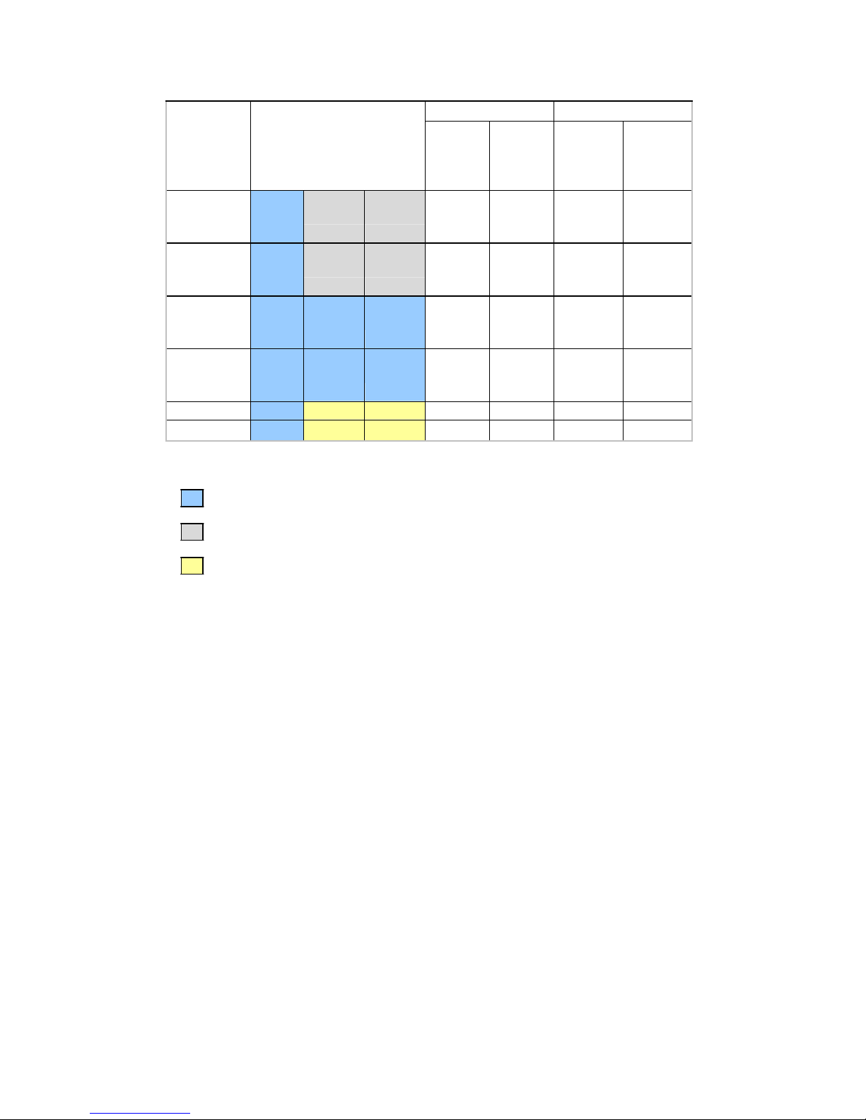
NOTE 1: The blue blocks indicate that the DRAM Densities are supported but no
t
validated.
NOTE 2:
The grey blocks indicate that the DRAM Densities are supported and validated.
NOTE 3:
The yellow blocks indicate that the DRAM Densities are supported with limited
validated.
Supported DRAM Densities are 1Gb, 2Gb and 4Gb. Only 2Gb and 4Gb are validated by
Intel.
Command Address Timing is 1N.
QR RDIMM are supported but not validated by Intel/PMO in a homogenous
environment. The coverage will have limited system level testing, no signal integrity
testing, and no interoperability testing. The passing QR RDIMMs will be web posted.
Page 36
36
Memory Installation Procedure
Caution: Ensure to unplug the power supply before adding or removing
DIMMs, or other system components, Failure to do so may cause severe
damage to both the motherboard and the components.
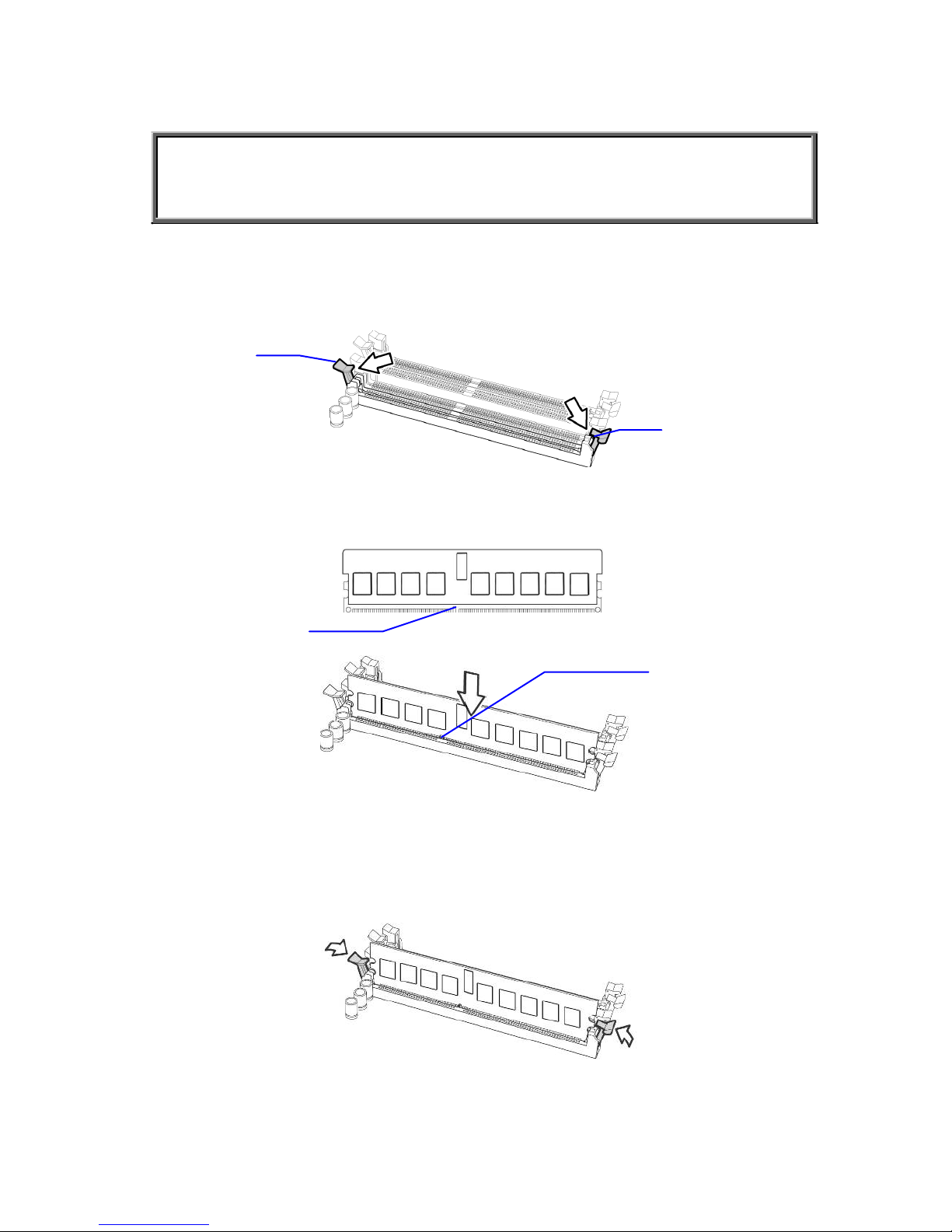
Follow these instructions to install memory modules into the WinFast WS1000.
1. Unlock a DIMM socket by Press the retaining clip outwardly in the following
illustration.
Unlocked
retaining
clip
Unlocked
retaining clip
2. Align the memory module with the socket,such that the DIMM NOTCH match
the KEY SLOT on the socket.
DIMM NOTCH
KEY SLOT
3. Hold the DIMM by both of its ends. Insert the module vertically into the socket.
Apply force to both ends of the DIMM simultaneously until the retaining clip pop
up into place. And the DIMM cannot be pushed in any further to ensure proper
sitting of the DIMM.
Page 37
37
2.8 - Attaching Drive Cables
WinFast WS1000 is equipped with 6 Serial ATA (SATA) channels. Connections for
the drives are very simple. There is no need to set Master/Slave jumpers on SATA
drives. distributor.
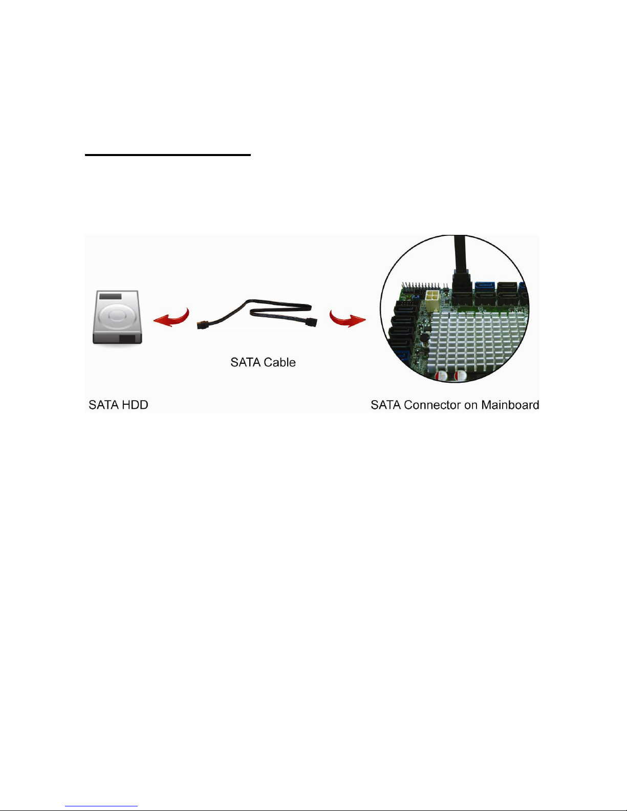
Attaching Serial ATA Cables
The following illustrates how to make a SATA Cable connection. If you are in need of
SATA/SAS cables or power adapters please contact your local sales representative.
Page 38
38
2.9 - Installing Add-In Cards
Before installing add-in cards, it’s helpful to know if they are fully compatible
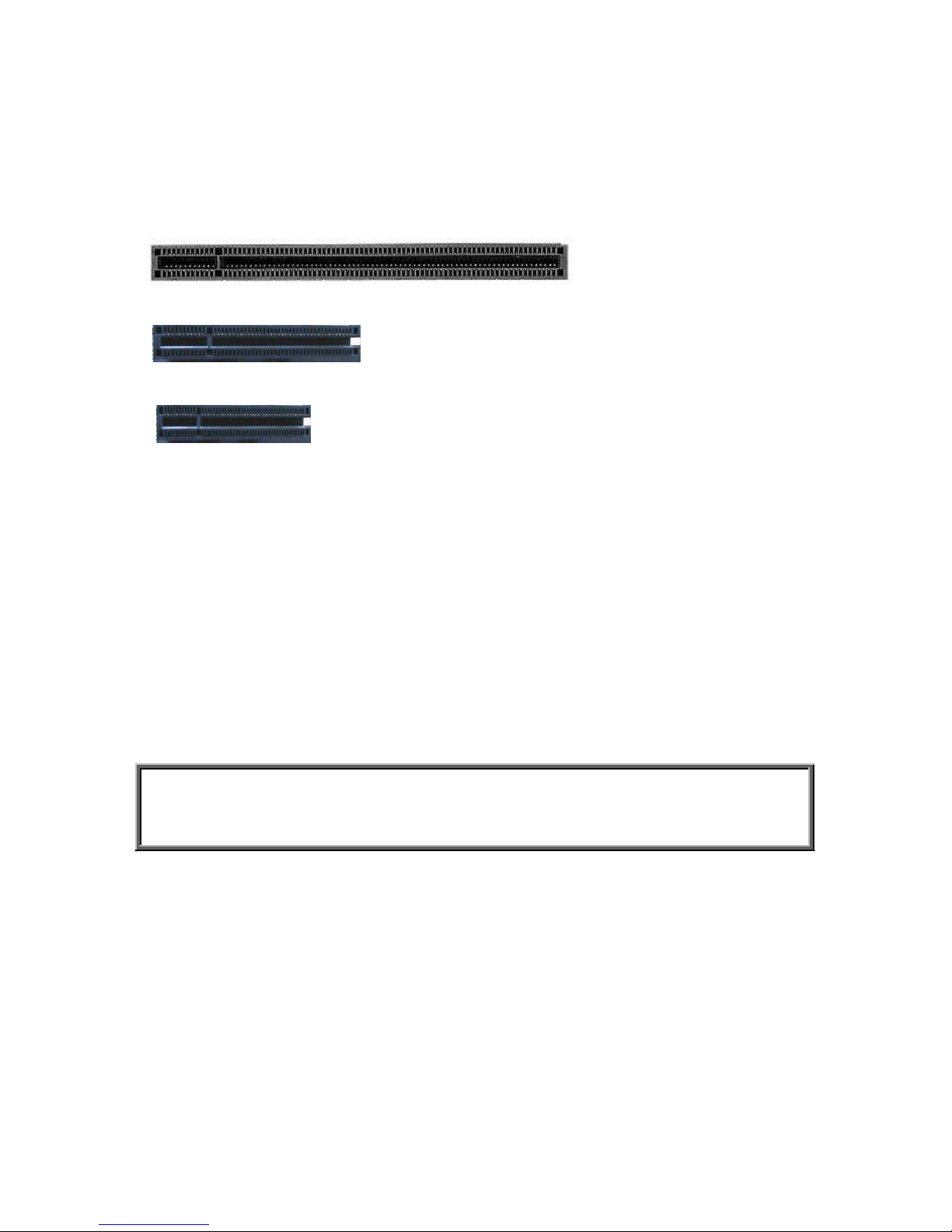
with your motherboard. For this reason, we’ve provided the diagrams below,
showing the slots that may appear on your motherboard.
PCI-E Gen3 x 16 slot
PCI-E Gen3 x 8 slot
PCI-E Gen3 x 4 slot
Simply find the appropriate slot for your add-in card and insert the card firmly. Do
not force any add-in cards into any slots if they do not seat in place. It is better to
try another slot or return the faulty card rather than damaging both the
motherboard and the add-in card.
TIP: It’s good practice to install add-in cards in a staggered manner rather than
making them directly adjacent to each other. Doing so allows air to circulate within
the chassis more easily, thus improving cooling for all installed devices.
NOTE: YOU MUST ALWAYS unplug the power connector to the motherboard
before performing system hardware changes to avoid damaging the board or
expansion device.
Page 39
39
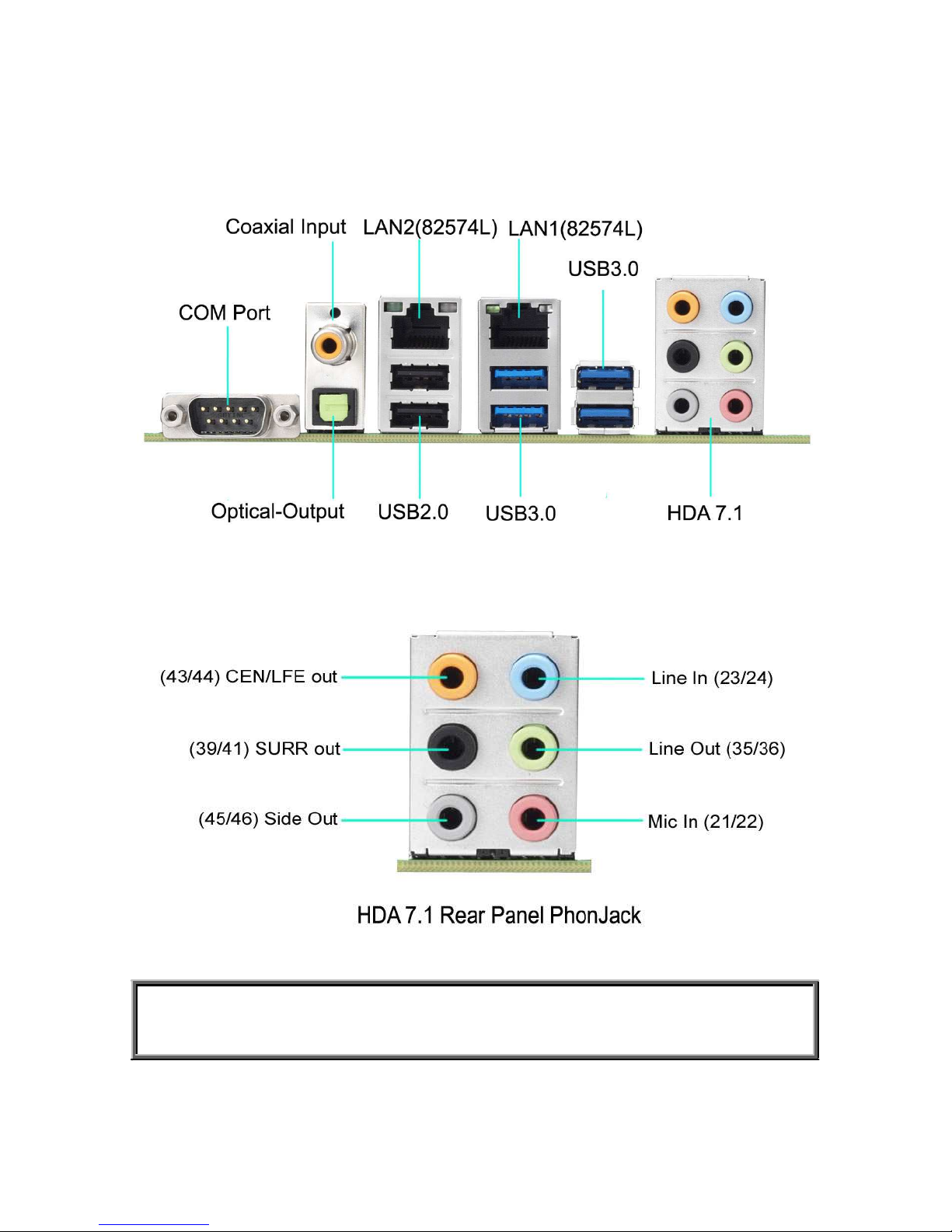
2.10 - Connecting External Devices
Your motherboard supports a number of different interfaces through connecting
peripherals. See the following diagrams for the details.
NOTE: Peripheral devices can be plugged straight into any of these ports but
software may be required to complete the installation.
Page 40
40
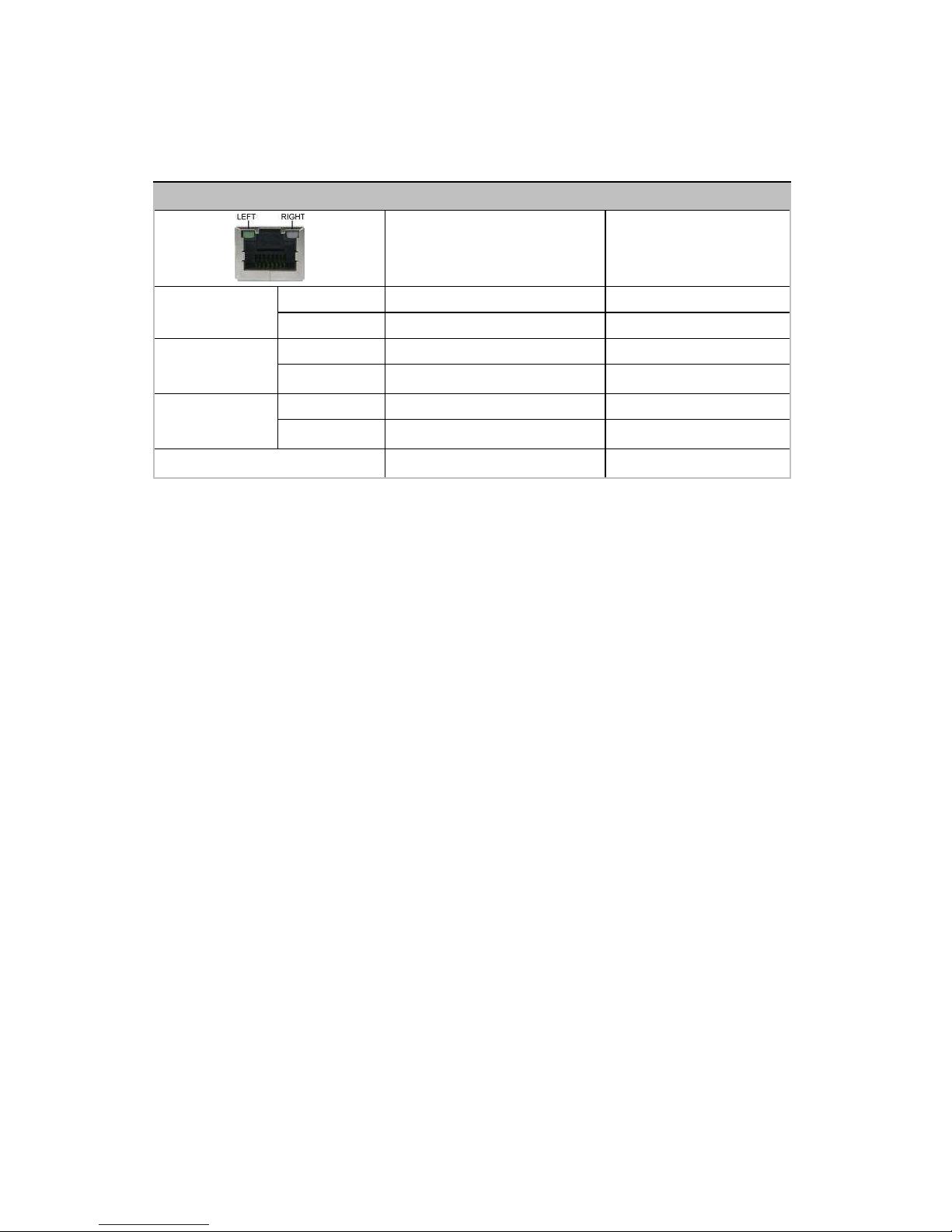
Onboard LAN LED Color Definition
The Two onboard Ethernet ports have green and amber LEDs to indicate LAN
status. The chart below illustrates the different LED states.
10/100/1000 Mbps LAN Link/Activity LED Scheme
Left LED
(Link/Activity)
Right LED
(Speed)
Link
Green
Off
10 Mbps
Active
Blinking Green
Off
Link
Green
Solid Green
100 Mbps
Active
Blinking Green
Solid Green
Link
Green
Solid Yellow
1000 Mbps
Active
Blinking Green
Solid Yellow
No Link
Off
Off
Page 41
41
2.11- Installing the Power Supply
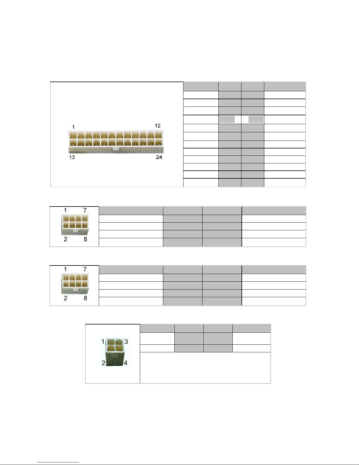
There are four (4) power connectors on your WinFast WS1000. It is required that
you have an EPS12V power supply has one 24-pin and two 8-pin connectors.
PW1: 24-Pin 12V main PWR Connector
Signal Pin Pin Signal
+3.3V
1
13
+3.3V
+3.3V
2
14
-12V
GND
3
15
GND
+5V
4
16
PS_ON#
GND
5
17
GND
+5V
6
18
GND
GND
7
19
GND
PWR OK
8
20
Reserve
5VSB
9
21
+5V
+12V
10
22
+5V
+12V
11
23
+5V
+3.3V
12
24
GND
PW2: 8-Pin PWR Connector
Signal
Pin Pin Signal
GND
1
2
GND
GND
3
4
GND
P12V_CPU0
5
6
P12V_CPU0
P12V_DDR3_CPU0
7
8
P12V_DDR3_CPU0
PW3: 8-Pin PWR Connector
Signal
Pin Pin Signal
GND
1
2
GND
GND
3
4
GND
P12V_CPU1
5
6
P12V_CPU1
P12V_DDR3_CPU1
7
8
P12V_DDR3_CPU1
PW4: 4-Pin PW Connector
Signal
Pin Pin Signal
GND
1
2
GND
+12V
3
4
+12V
NOTE:
The PW4 is reserved for PCIE slot
12V supplement if the PCIE card and the MB
FAN's 12V power consumption exceed the
maximum 12V out of PSU's PW1.
Page 42

42
NOTE: YOU MUST unplug the power supply before plugging the power cables
to motherboard connectors.
2.12 - Finishing Up
Congratulations on making it this far! You’re finished setting up the hardware
aspects of your computer. Before closing up your chassis, make sure that all cables
and wires are connected properly, especially power cables and most importantly
jumpers. You may have difficulty powering on your system if the motherboard
jumpers are not set correctly. In the rare circumstance that you have experienced
difficulty, you can find help by asking your vendor for assistance. If they are not
available for assistance, please find setup information and documentation online
at our website or by calling your vendor’s support line.
Page 43
43
Chapter 3: BIOS Setup
3.1 - About the BIOS
The BIOS is the basic input/output system, the firmware on the motherboard that
enables your hardware to interface with your software. The BIOS determines what a
computer can do without accessing programs from a disk. The BIOS contains all the
code required to control the keyboard, display screen, disk drives, serial
communications, and a number of miscellaneous functions. This chapter describes
the various BIOS settings that can be used to configure your system.
The BIOS section of this manual is subject to change without notice and is provided
for reference purposes only. The settings and configurations of the BIOS are
current at the time of print and are subject to change, and therefore may not match
exactly what is displayed on screen.
This section describes the BIOS setup program. The setup program lets you modify
basic configuration settings. The settings are then stored in a dedicated, batterybacked memory (called NVRAM) that retains the information even when the power is
turned off.
To start the BIOS setup utility:
1. Turn on or reboot your system.
2. Press <Del> during POST (<Tab> on remote console) to start the BIOS
setup utility.
3.2 - Setup Basics
The table below shows how to navigate in the setup program using the keyboard.
Key
Function
<F1> General help window
<ESC> Exit current menu
arrow keys Select a different menu
↑
or ↓ arrow keys
Move cursor up/down
<Tab> / <Shift-Tab> Cycle cursor up/down
<Home> / <End> Move cursor to top/bottom of the window
<PgUp> / <PgDn> Move cursor to next/previous page
<-> Select the previous value/setting of the field
<+> Select the next value/setting of the field
<F8> Load Fail Safe default configuration values of the
menu
<F3> Load the Optimal default configuration values of
the menu
<F4> Save and exit
<Enter> Execute command or select submenu
Page 44

44
3.3 - Getting Help
Pressing [F1] will display a small help window that describes the appropriate keys
to use and the possible selections for the highlighted item. To exit the Help Window,
press [ESC].
3.4 - In Case of Problems
If you have trouble booting your computer after making and saving the changes
with the BIOS setup program, you can restart the computer by holding the power
button down until the computer shuts off (usually within 4 seconds); resetting by
pressing CTRL-ALT-DEL; or clearing the CMOS. The best advice is to only alter
settings that you thoroughly understand. In particular, do not change settings in the
Chipset section unless you are absolutely sure of what you are doing. The Chipset
defaults have been carefully chosen either by Leadtek or your system
manufacturer for best performance and reliability. Even a seemingly small change
to the Chipset setup options may cause the system to become unstable or
unusable.
NOTE: The following pages provide the details of BIOS menu. Please be noticed
that the BIOS menu are continually changing due to the BIOS updating. The BIOS
menu provided are the most updated when this manual is written. Please visit
Leadtek’s website at http://www.leadtek.com for the information of BIOS updating.
Page 45
45
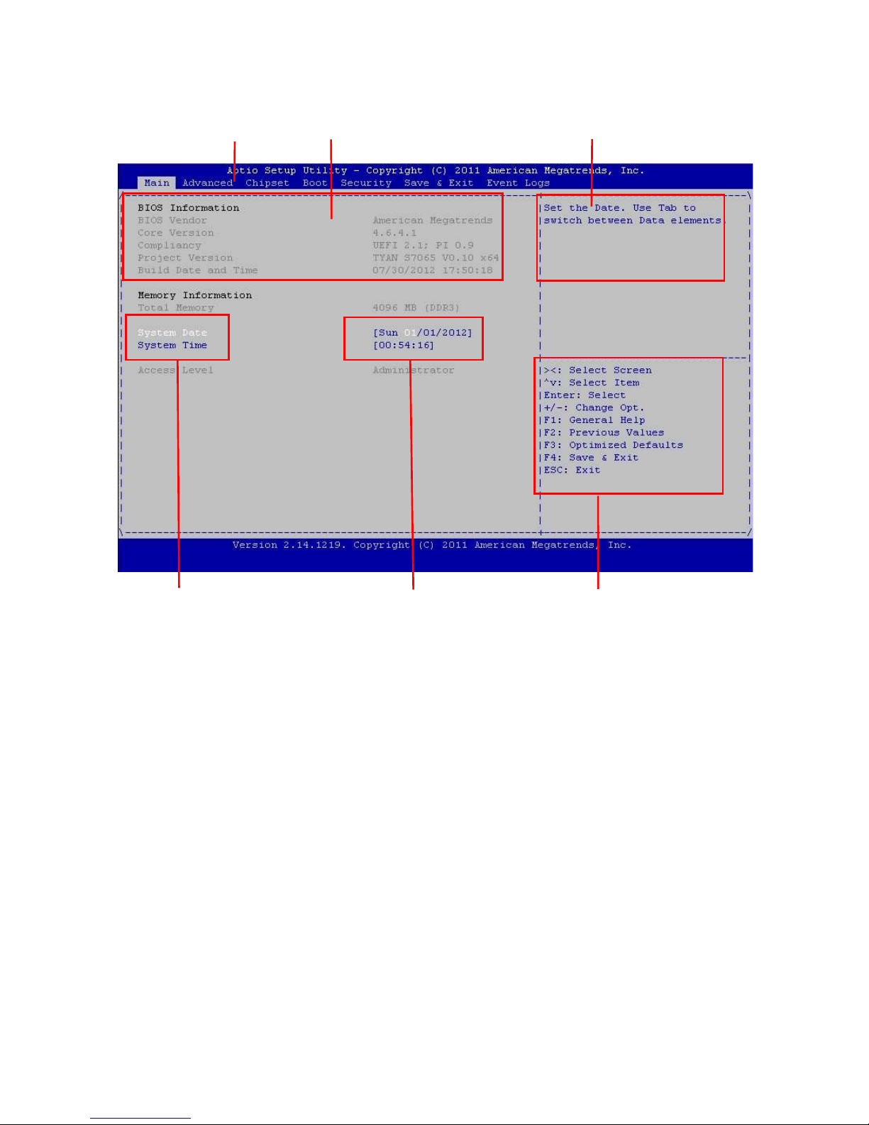
3.5 - BIOS Main Menu
Manual Bar
Specification
General help
Sub-menu items
BIOS Information
Configuration fields Navigation keys
Displays BIOS related information.
Memory Information
Displays total memory size.
System Date (Day dd/mm/yyyy)
System Time (hh:mm:ss)
Allow user to set system time and date.
The Time is displayed in 24 hours format.
The Date can be set from January 1st, 2005 to December 31, 2099
The values set in these two fields take effect immediately.
Page 46

46
3.5.1 Manual Bars
Main
For changing the basic system configuration
Advanced
For changing the advanced system settings
Chipset
For customize the Intel chipset function
Boot
For changing the system boot configuration
Security
For setting the Supervisor and User passwords
Server Mgmt
For changing the server management
Event Logs
For record the system Event Logs
Save & Exit
For selecting the exit options and loading default
settings
NOTE: The Main BIOS Menu is the first screen that you can navigate which has
two main frames. The left frame displays all the options that can be configured.
"Grayed-out" options cannot be configured, options in blue can be changed. The
right frame displays the key legend. Above the key legend is an area reserved for
a text message. When an option is selected in the left frame, it is highlighted in
white. Often, a text message will accompany it.
Page 47
47
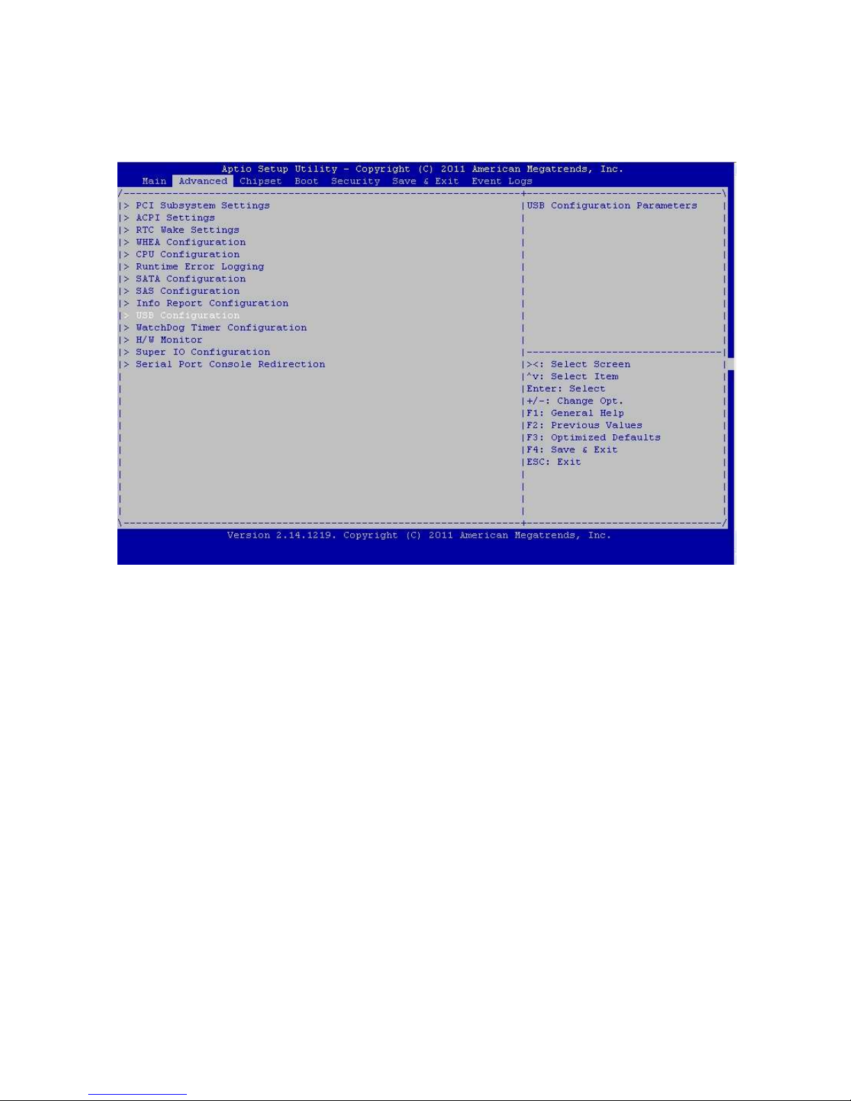
3.6 - BIOS Advanced Menu
This section facilitates configuring advanced BIOS options for your system.
PCI Subsystem Settings
PCI,PCI-X and PCI Express Configuration.
ACPI Settings
Selection for Advanced ACPI Configuration.
RTC Wake Settings
Selection for RTC Wake Configuration.
WHEA Configuration
General WHEA Configuration Setting.
CPU Configuration
CPU Configuration Parameters.
Runtime Error Logging
Runtime Error Logging Support Setup Options
SATA Configuration
This menu helps you to set up or change the SATA Configuration.
Page 48

48
SAS Configuration
SAS Devices Configuration.
Info Report Configuration
Info report configure
USB Configuration
Configure the USB support
Watchdog Timer Configuration
Configure watchdog Timer
H/W Monitor Configuration
IPMI configuration including server monitoring and event log
Super IO Configuration
Configures Super IO
Serial Port Console Redirection
Redirect Serial Port Console
Page 49
49
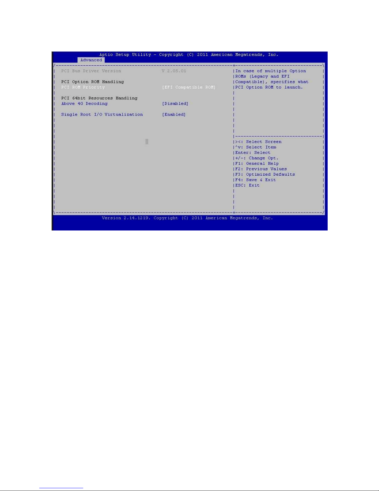
3.6.1 - PCI Setting
PCI Option ROM Handling
PCI ROM Priority
In case of multiple option ROMs (Legacy and EFI compatible), specifies what PCI
option ROM to launch.
[EFI Compatible ROM] / [Legacy ROM]
Default is [EFI Compatible ROM]
PCI 64bit Resources Handling
Above 4G Decoding
Enables or disables 64 bit capable devices to be decoded in above 4G address
space(only if system supports 64 bit PCI decoding.
[Disabled] / [Enabled]
Default is [Disabled]
Single Root I/O Virtualization
Enable or disable single Root I/O virtualization
[Disabled] / [Enabled]
Default is [Enabled]
Page 50
50
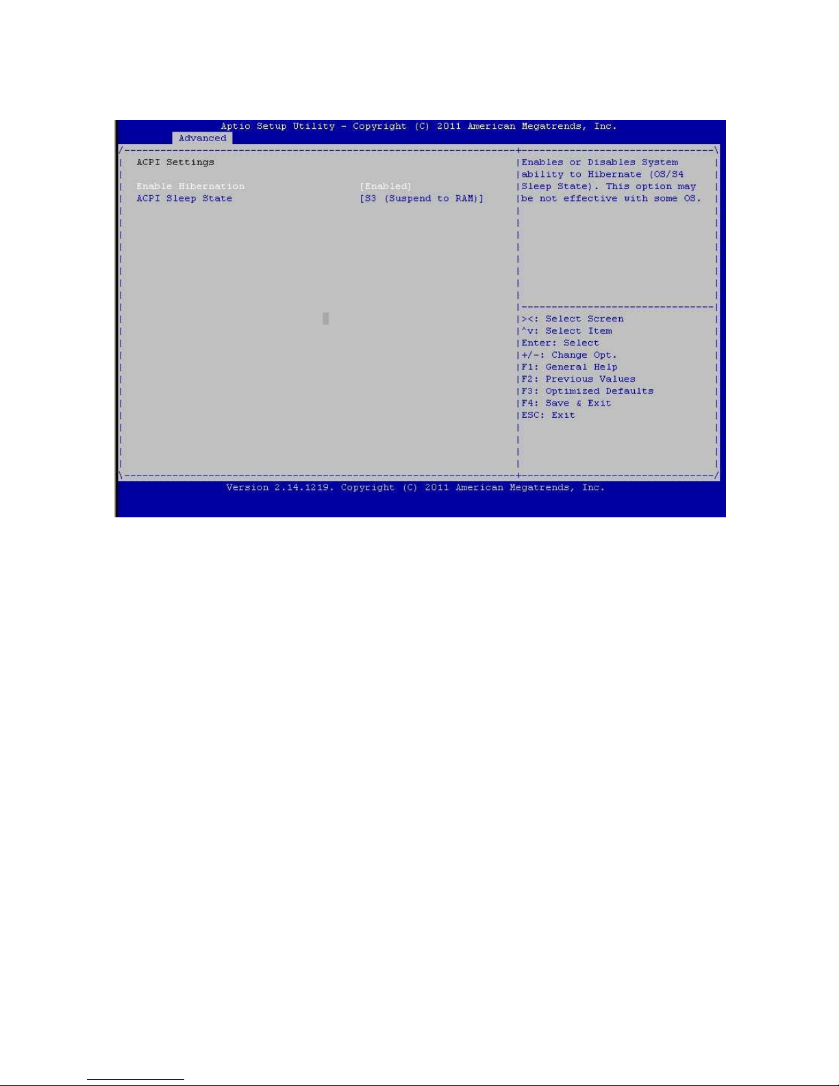
3.6.2 - ACPI Setting
Enable Hibernation
Enables or disables System ability to Hibernate (OS/S4 sleep state). This option may
be not effective with some OS.
[Disabled] / [Enabled]
Default is [Enabled]
ACPI Sleep State
Select the highest ACPI sleep state the system will enter when the suspend button
is pressed.
[Suspend Disabled] / [S1(CPU Stop Clock)] / [S3(suspend to RAM)]
Default is [S3(suspend to RAM)]
Page 51
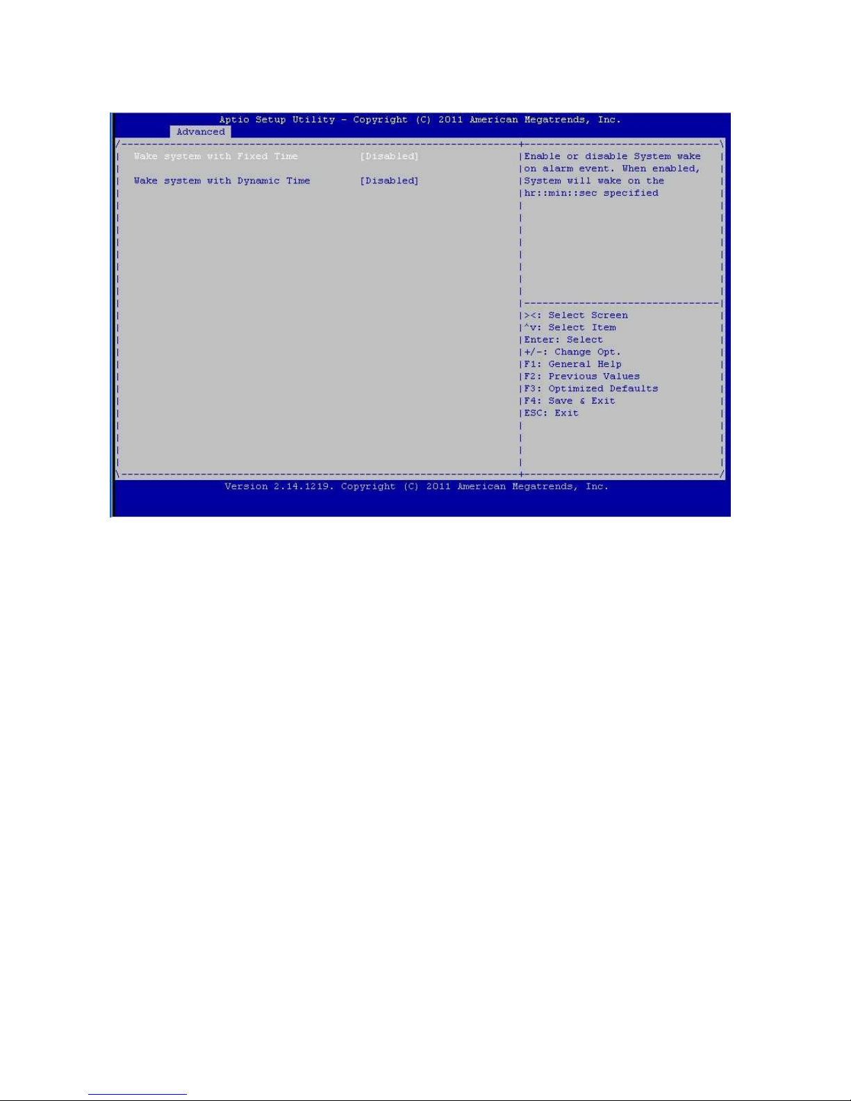
51
3.6.3 – Wake system Configuration
Wake system with Fixed Time
Enable or disable system wake on alarm event. When enabled, system will wake on
the hr :: min :: sec specified
[Disabled] / [Enabled]
Default is [Disabled]
Wake system with Dynamic Time
Enable or disable system wake on alarm event. When enabled, system will wake on
the hr :: min :: sec specified
[Disabled] / [Enabled]
Default is [Disabled]
Page 52
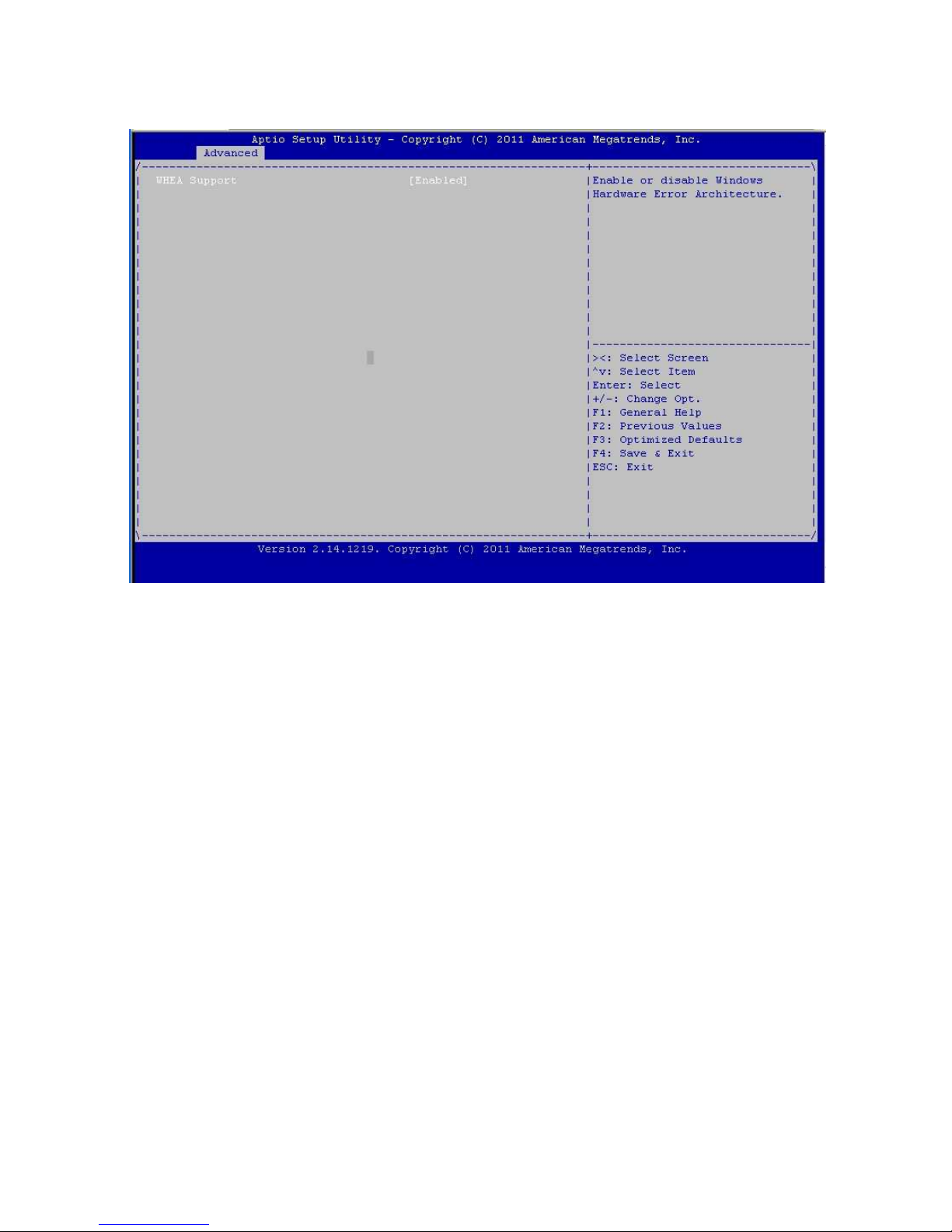
52
3.6.4 - WHEA Support
WHEA Support
Enables or disables Windows Hardware Error Architecture.
[Disabled] / [Enabled]
Default is [Enabled]
Page 53
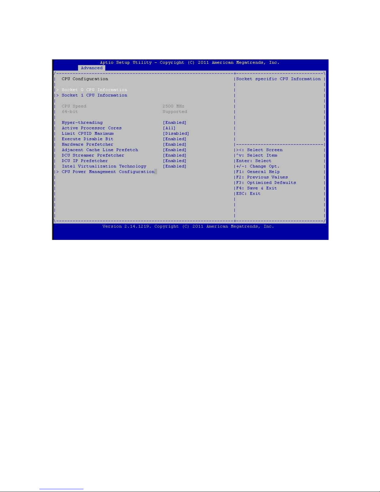
53
3.6.5 - CPU Configuration
This section allows you to fine-tune the processor options.
Hyper- threading
This option enable for Windows XP and Linux (OS optimized for Hyper- threading
Technology.
And Disabled for other (OS not optimized for Hyper-threading Technology).
[Disabled] / [Enabled]
Default is [Enabled]
Active Processor Core
[All]/[1]/[2]/[3]/[4]/[5]/[6]/[7]
Default is [All]
Limit CPUID Maximum
[Disabled] / [Enabled]
Default is [Disabled]
Execute Disable Bit
[Disabled] / [Enabled]
Default is [Enabled]
Hardware Prefetcher
[Disabled] / [Enabled]
Default is [Enabled]
Page 54

54
Adjacent Cache Line Prefetch
[Disabled] / [Enabled]
Default is [Enabled]
DCU Streamer Prefetcher
Enable prefetch of next L1 Data line based upon multiple loads in same cache line.
[Disabled] / [Enabled]
Default is [Enabled]
DCU IP Prefetcher
Enable prefetch of next L1 line based upon sequential load history.
[Disabled] / [Enabled]
Default is [Enabled]
Intel Virtualization Technology
When enabled, a VMM can utilize the additional hardware capabilities provided by
Vanderpool Technology.
NOTE: Once the lock bit is set, the contents of this register can not be modified until
S5 reset occurs.
[Disabled] / [Enabled]
Default is [Enabled]
Page 55
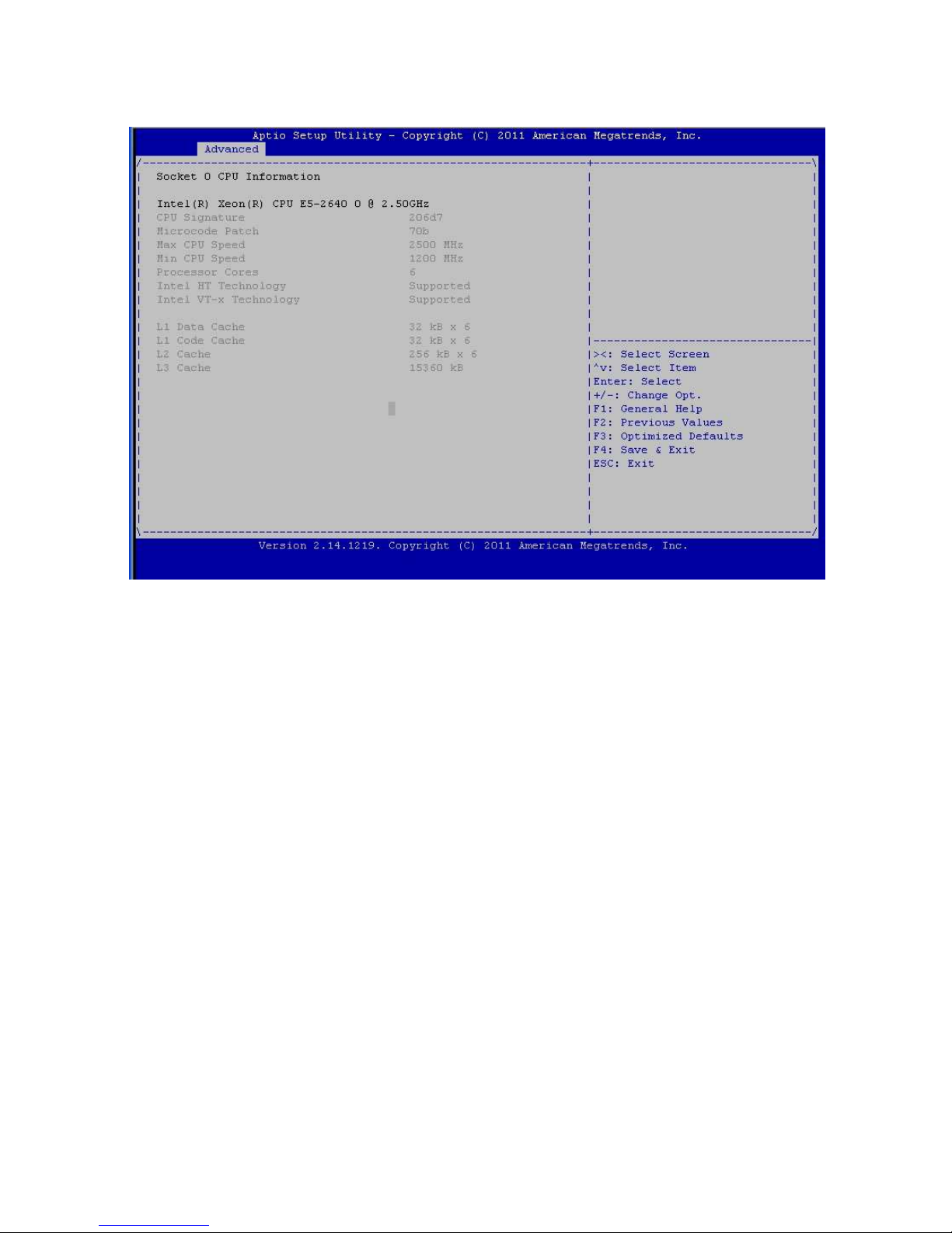
55
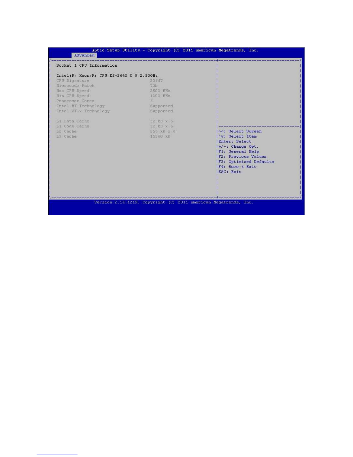
3.6.5.1 – Socket0 CPU Configuration
Read only
Page 56
56
3.6.5.2 – Socket1 CPU Configuration
Read Only
Page 57
57
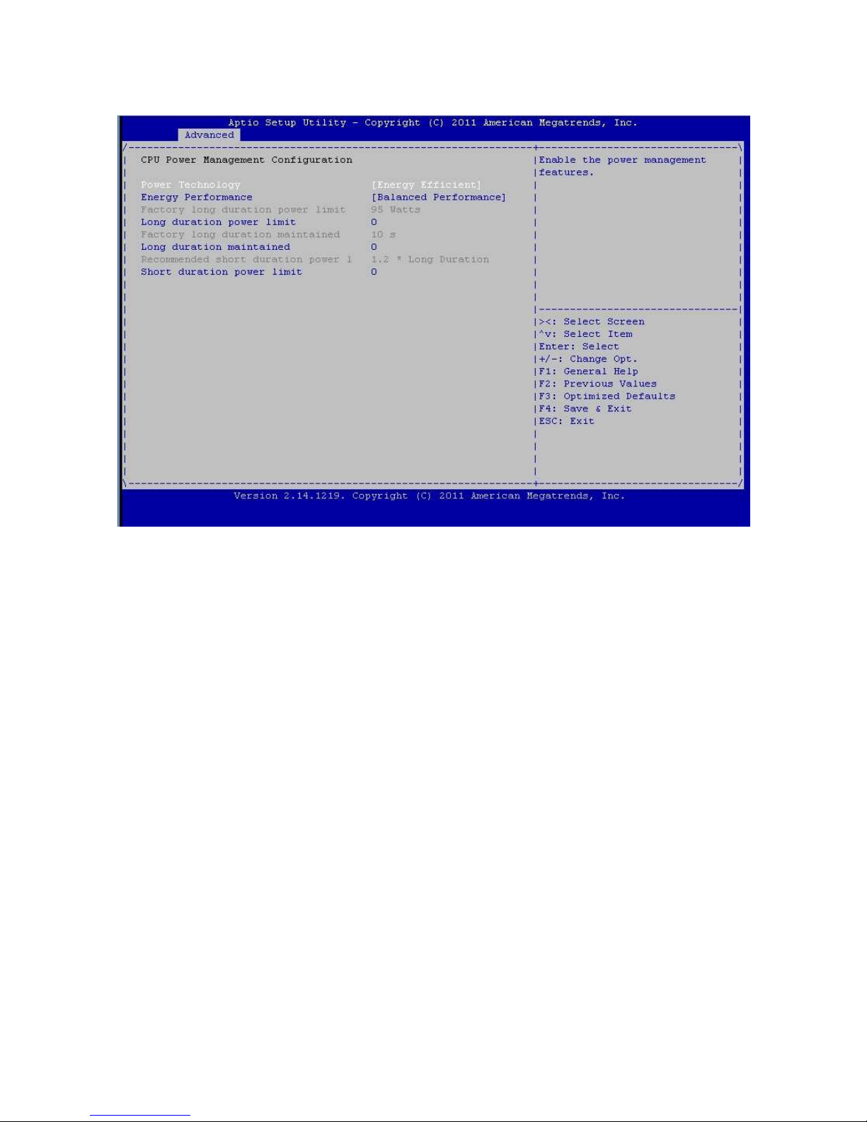
3.6.5.3 - CPU Power Management Configuration
Power Technology
Enable the power management features.
[Disable] / [Energy Efficient] / [Custom]
Default is [Energy Efficient]
Energy Performance
Optimize between Performance and power savings. Windows 2008 and later OSes
overrides this value according to its power plan.
[Performance] / [Balanced Performance] / [Balanced Energy]
Default is [Balanced Performance]
Factory Long Duration
Read only.
Long Duration power
Time window which the long duration power is maintained.
Factory Long Duration
Read only.
Long Duration Maintained
Time window which the long duration power is maintained.
Page 58
58
Recommended short duration power limit
Read only.
Short duration power limit
Short duration power limit in Watts.
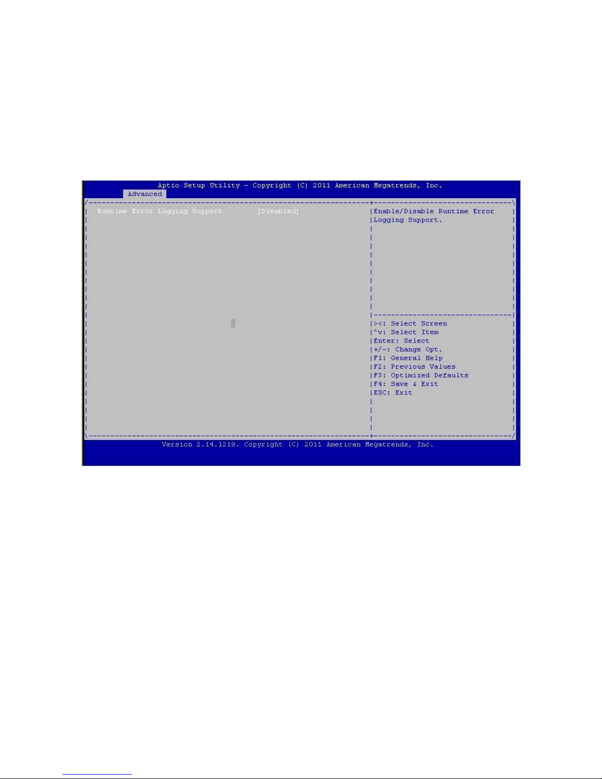
3.6.6 – Runtime Error Logging Configuration
Runtime Error Logging Support
Enable/Disable Runtime Error Logging Support.
[Enabled] / [Disabled]
Default is [Disabled]
Page 59
59
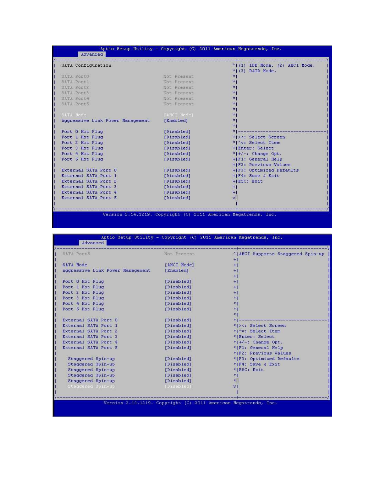
3.6.7 - SATA Configuration
External SATA port0/1/2/3/4/5
Enable/Disable SATA Ports Hot Plug Support.
[Enabled] / [Disabled]
Default is [Disabled]
Page 60

60
SATA Mode
Select SATA Mode.
[IDE Mode] / [AHCI Mode] / [RAID Mode] / [Disabled]
Default is [AHCI Mode]
Agressive Link Power Management
[Enabled] / [Disabled]
Default is [Enabled]
Port1/2/3/4/5 Hot Plug
[Enabled] / [Disabled]
Default is [Disabled]
External SATA Port 0/1/2/3/4/5
[Enabled] / [Disabled]
Default is [Disabled]
Staggered Spin-up
AHCI Supports Staggered Spin-up
[Enabled] / [Disabled]
Default is [Disabled]
Page 61
61
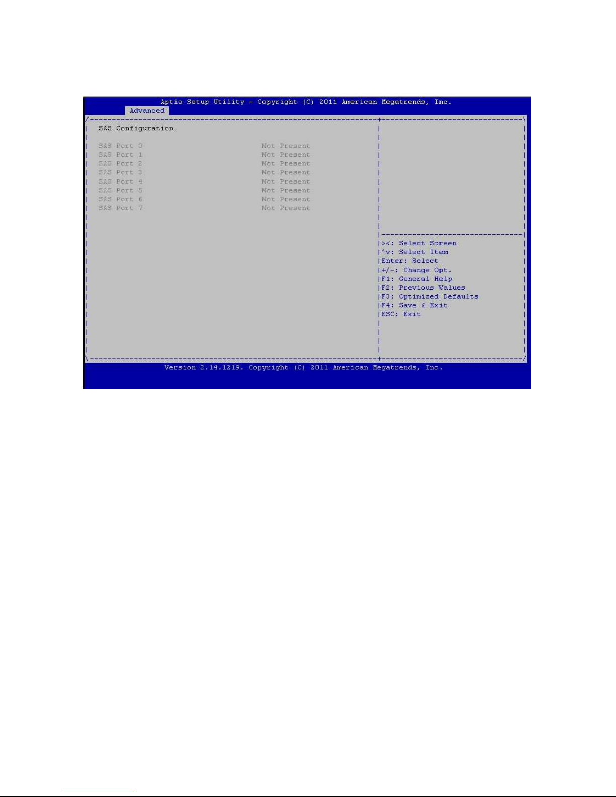
3.6.8 - SAS Configuration
Read only.
Page 62
62
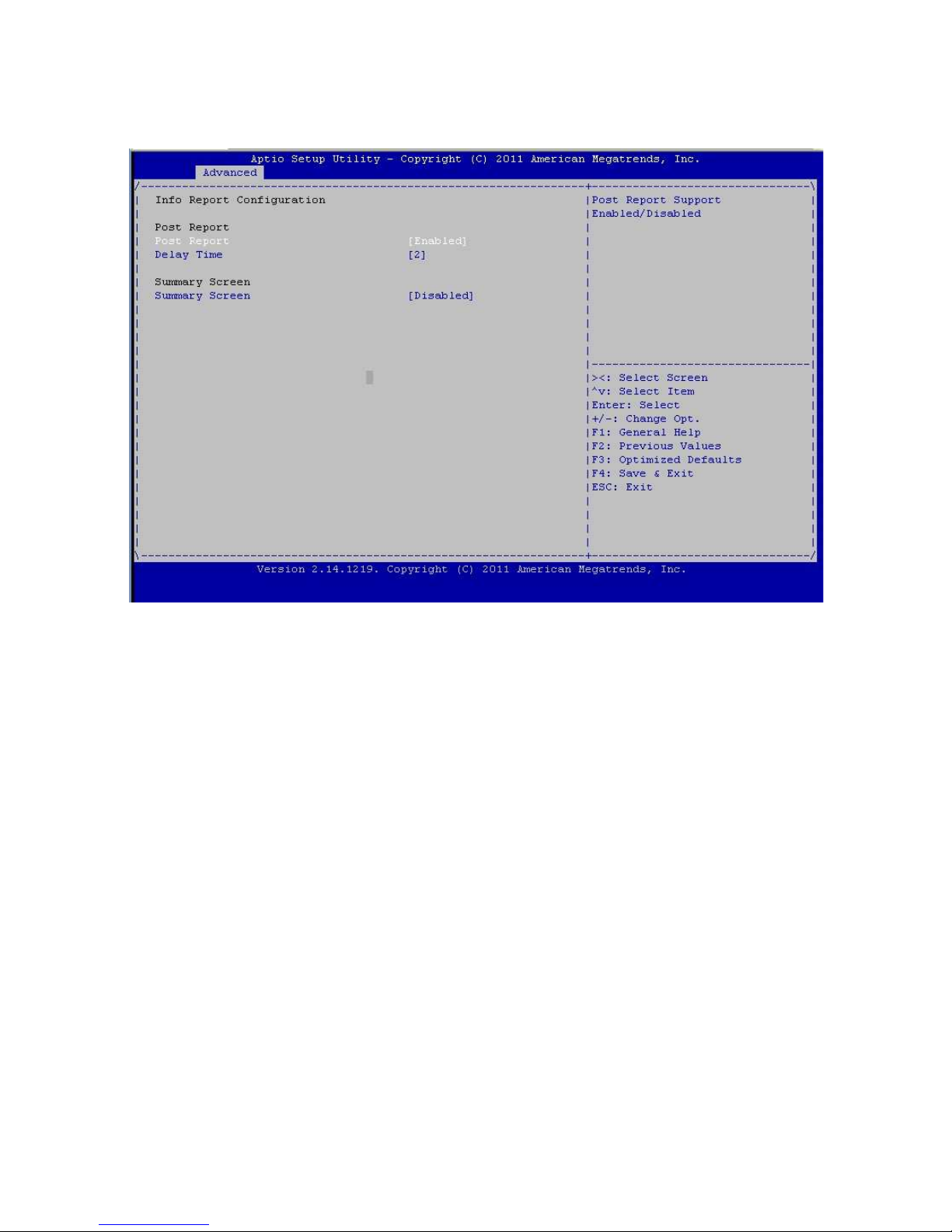
3.6.9 Info Report Configuration
Post Report
Post report support enabled/disabled
[Enabled] / [Disabled]
Default is [Enabled]
Delay Time
Post report support enabled/disabled
[0]/[1]/[2]/[3]/[4]/[5]/[6]/[7]/[8]/[9]/[10]/[Until press ESC]
Default is [2]
Summary Screen
[Enabled] / [Disabled]
Default is [Disabled]
Page 63
63
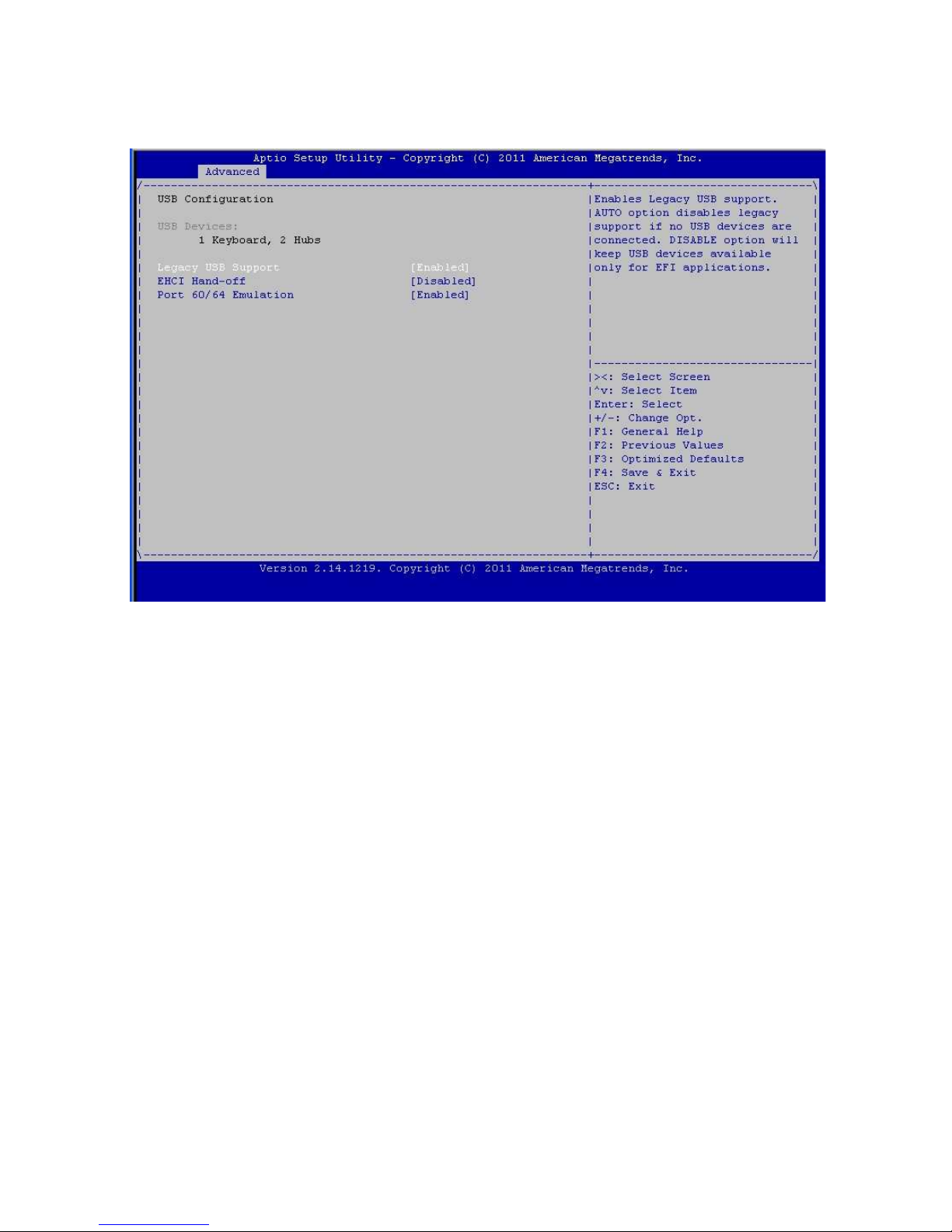
3.6.10 USB Configuration
Legacy USB Support
Enables legacy USB support, Auto option disables legacy support if no USB devices
are connected. Disable option will keep USB devices available only for EFI
applications.
[Disabled] / [Enabled] / [Auto]
Default is [Enabled]
EHCI Hand-off
[Disabled] / [Enabled]
Default is [Disabled]
Port 60/ 64 Emulation
Enables IO port 60h/64h emulation support This should be enabled for the
Complete USB keyboard legacy support for non-USB aware OSes.
[Disabled] / [Enabled]
Default is [Enabled]
Page 64
64
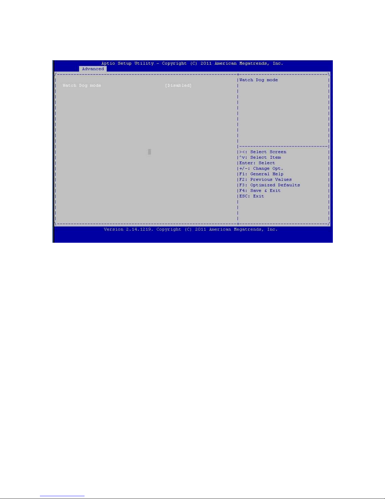
3.6.11– Watchdog Timer Configuration
Watchdog mode
[Disable] / [Post] / [OS] / [Power ON]
Default is [Disabled]
Page 65
65
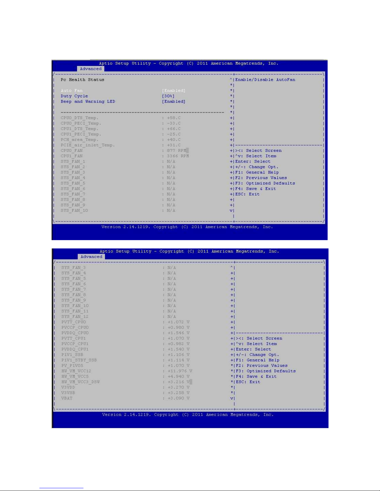
3.6.12 – Hardware Health Configuration
Page 66

66
Auto Fan
[Disabled] / [Enabled]
Default is [Enabled]
The disable meaning is FAN Speed running FULL ON
Duty Cycle
[30% Duty Cycle] / [45% Duty Cycle] / [60% Duty Cycle]
Default is [30% Duty Cycle]
Beep and warning LED
[Enabled] / [Disabled]
Default is [Enabled]
*The Fan data need set Auto Fan to [Enabled]’
Page 67
67
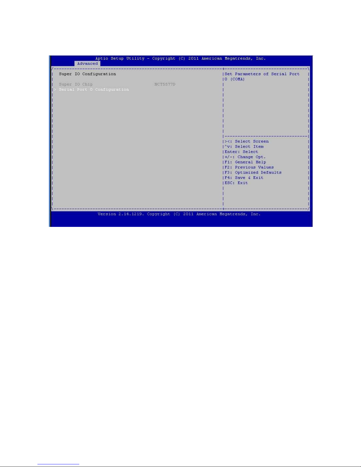
3.6.13 Super I/O Configuration
Super IO Chip
Read only.
Page 68
68
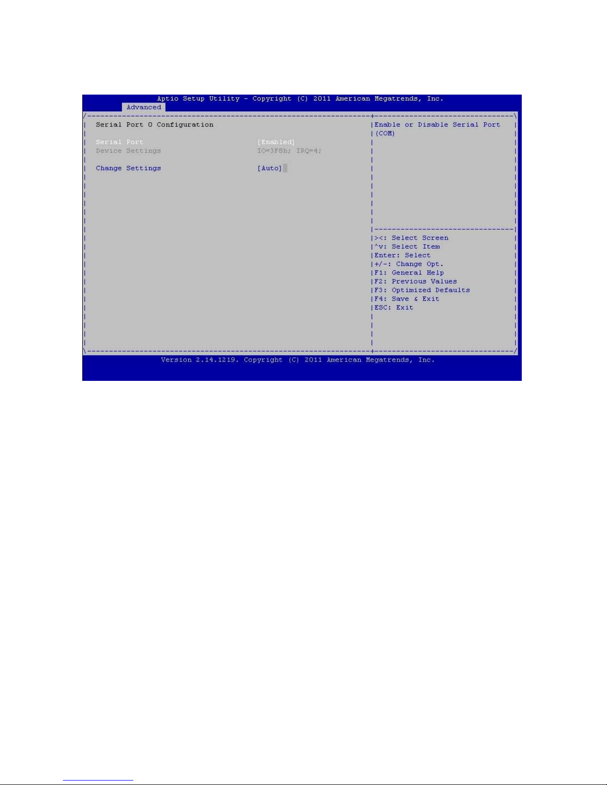
3.6.13.1 Serial port submenu
Serial Port 0 Configuration
Serial Port
Enable or Disable Serial Port (COM)
[Enabled] / [Disabled]
Default is [Enabled]
Device Settings
Read only. It can not be modified in user mode.
Change/Settings
Select an optimal setting for super I/O device.
[Auto] / [I/O=3F8h;IRQ=4] / [ I/O=3F8h;IRQ=3,4,5,6,7,8,9,10,11,12]/
[ I/O=2F8h;IRQ=3,4,5,6,7,8,9,10,11,12] / [ I/O=3E8h;IRQ=3,4,5,6,7,8,9,10,11,12]/
[ I/O=2E8h;IRQ=3,4,5,6,7,8,9,10,11,12]
Default is [Auto]
Page 69
69
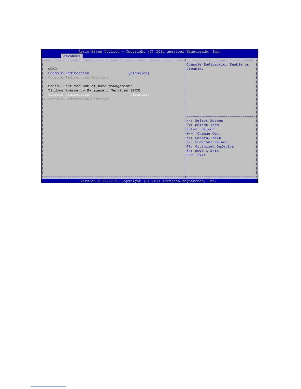
3.6.14 Serial Port Console Redirection
Console Redirection
Console redirection enable or disable.
[Disabled] / [Enabled]
Default is [Disabled]
Serial Port for Out-Of-Band Management/Windows Emergency Services (EMS)
Console Redirection
Console redirection enable or disable.
[Disabled] / [Enabled]
Default is [Disabled]
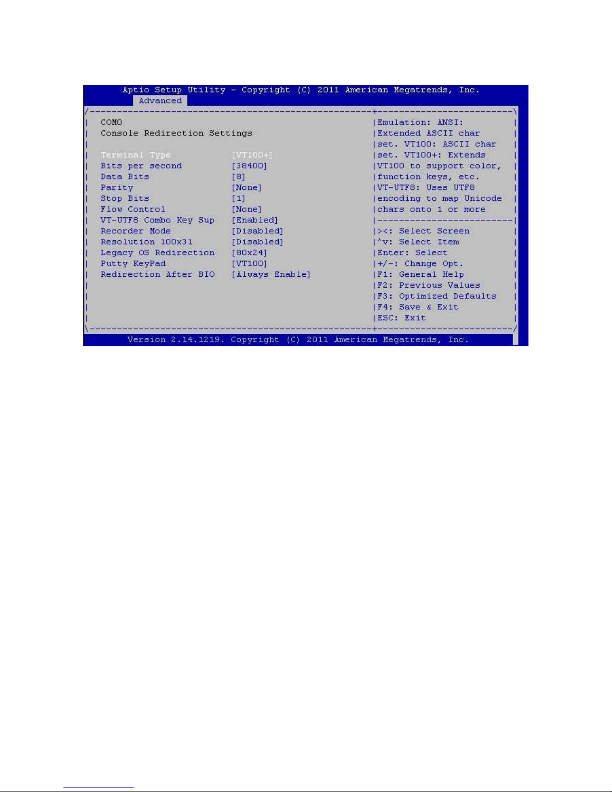
Console Redirection Settings
The settings specify how the host computer (which the user is using) will exchange
data. Both computers should have the same or compatible settings.
Page 70
70
3.6.14.1 Console Redirection Submenu
Terminal Type
Emulation: ANSI: Extended ASCII charset.
VT100: ASCII charset.
VT100+: Extends VT100 to support color function keys, etc.
VT-UTF8: Uses UTF8 encoding to map Unicode chars onto 1 or more bytes.
[VT100] / [VT100+] / [VT-UTF8] / [ANSI]
Default is [VT100+]
Bits per second
Selects serial port transmission speed. The speed must be matched on the other
side. Long or noisy lines may require lower speeds.
[9600] / [19200] / [38400] / [57600] / [115200]
Default is [38400]
Data Bits
[7] / [8]
Default is [8]
Parity
A parity bit can be sent with the data bits to detect some transmission errors.
Even: Parity bit is 0 if the num of 1’s in the data bits is even.
Odd: parity bit is 0 if the num of 1’s in the data bits is odd.
[None] / [Even] / [Odd] / [Mark] / [Space]
Default is [None]
Page 71

71
Stop Bits
Stop bits indicate the end of a serial data packet. (A start bit indicates the
beginning). The standard setting is 1 stop bit.1 communication with slow devices
may require more than 1.
[1] / [2]
Default is [1]
Flow Control
Flow control can prevent data loss from buffer overflow. When sending data, If the
receiving buffers are full, a ‘stop’ signal can be sent to stop the data flow. Once the
buffers are empty, a ‘start’ signal can be sent to restart the flow. Hardware flow
control uses two wires to send start/stop signal.
[None]
/
[Hardware RTS/CTS]
Default is [None]
VT-UTF8 Combo Key Support
Enable VT-UTF8 Combination Key Support for ANSI/VT100 terminals.
[Enabled] / [Disabled]
Default is [Enabled]
Recorder Mode
With this mode enabled only text will be sent. This is to capture Terminal data.
[Disabled] / [Enabled]
Default is [Disabled]
Resolution 100x31
Enable or disable extended terminal resolution.
[Disabled] / [Enabled]
Default is [Disabled]
Legacy OS Redirection Resolution
On Legacy OS, the number of rows and columns supported redirection.
[80x24] / [80x25]
Default is [80x24]
Putty KeyPad
Select FunctionKey and KeyPad on Putty.
[VT100] / [LINUX] / [XTERMR6] / [SCO] / [ESCN] / [VT400]
Default is [VT100]
Page 72
72
Redirection After BIOS POST
The settings specify if bootloader is selected than Legacy console redirection is
disabled before booting to Legacy OS. Default value is always enable means
Legacy.
[Always enable] / [Bootloader]
Default is [Always enable]
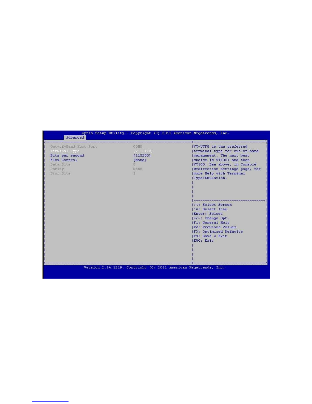
3.6.14.2 Serial Port for Out-Of-Band Management/Windows Emergency
Services (EMS) Console Redirection Settings
Out-of Band Mgmt Port COM0
Only read
Terminal Type
VT-UTF8 is the preferred terminal type for out-of-band management. The next best
choice is VT100+ and then VT100. See above, in Console Redirection Settings page,
for more Help with Terminal Type/Emulation.
[VT-UTF8] / [VT100] / [VT100+] / [ANSI]
Default is [VT-UTF8]
Page 73

73
Bits per Second
Select serial port transmission speed. The speed must be matched on the other
side. Long or noisy lines may require lower speeds.
[115200] / [9600] / [19200] / [57600]
Default is [115200]
Flow Control
Flow Control can prevent data loss from buffer overflow. When sending data, if the
receiving buffers are full, a ‘stop’ signal can be sent to stop the data flow. Once the
buffers are empty, a ‘start’ signal can be sent to restart the flow. Hardware flow
control uses two wires to send start/stop signal.
[None] / [Hardware RTS/CTS] / [SoftwareXon/Xoff]
Default is [None]
Data Bits / Parity / Stop Bits
Read only.
Page 74
74
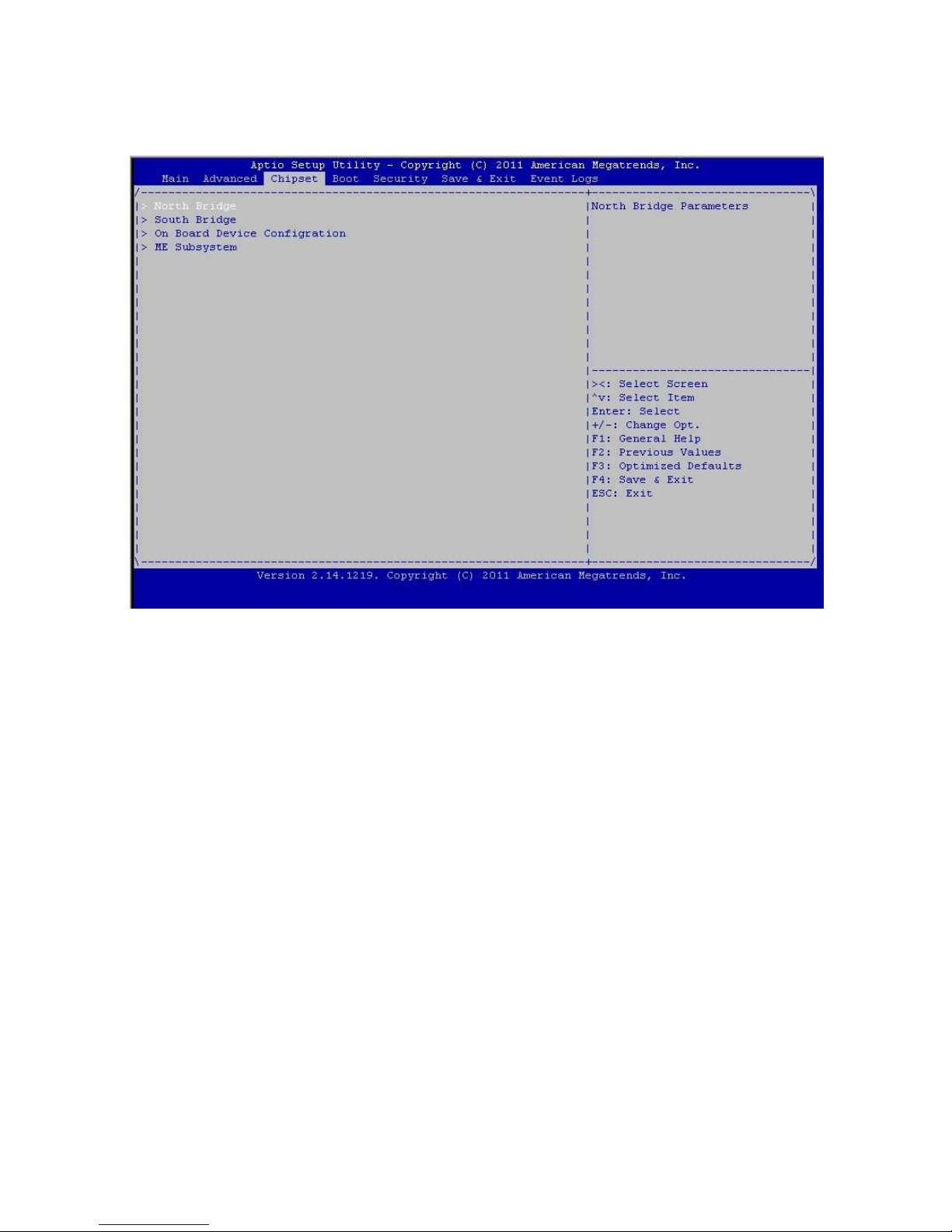
3.7 - Chipset Menu
North Bridge
North Bridge Parameters.
South Bridge
South Bridge Parameters.
Onboard Device Configuration
Configure Onboard Device
ME Subsystem
ME Subsystem Configuration
Page 75
75
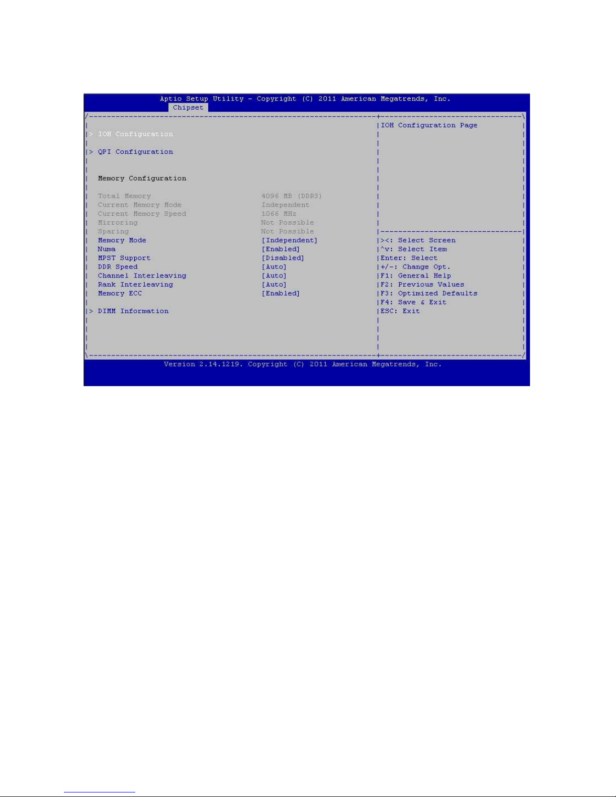
3.7.1 – North Bridge Chipset Configuration Sub- Menu
Total Memory / Current Memory Mode / Current Memory Speed / Mirroring /
Sparing
Read only.
Memory Mode
Select the mode for memory initialization.
[Independent] / [Mirroring] / [Lock Step] / [Sparing]
Default is [Independent]
Numa
Enable or disable Non uniform Memory Access (NUMA).
[Enabled] / [Disabled]
Default is [Enabled]
MPST Support
Enable or disable MPST Support. Along with enabling MPST Support, it also requires
NUMA to be enabled and channel Interleaving to be set to 1-way for MPST tables to
be published.
[Enabled] / [Disabled]
Default is [Disabled]
Page 76

76
DDR Speed
Force DDR Speed.
[Auto] / [Force DDR3 800] / [Force DDR3 1066] / [Force DDR3 1333] / [Force DDR3
1600] / [Force DDR3 1866]
Default is [Auto]
Channel Interleaving
Select different Channel Interleaving setting.
[Auto] / [1 Way] / [2 Way] / [3 Way] / [4 Way]
Default is [Auto]
Rank Interleaving
Select different rank Interleaving setting.
[Auto] / [1 Way] / [2 Way] / [4 Way] / [8 Way]
Default is [Auto]
Memory ECC
Enable/Disable Memory ECC.
[Enabled] / [Disabled]
Default is [Disabled]
Default is [Enabled]
Page 77
77
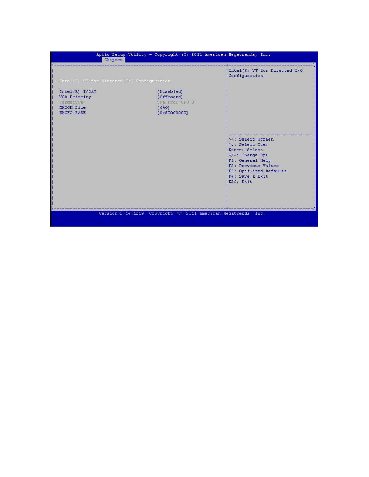
3.7.1.1 IOH Configuration Submenu
Intel® I/OAT
Enable/Disable Intel
®
I/O Acceleration Technology (I/OAT).
[Disabled] / [Enabled]
Default is [Disabled]
VGA Priority
Decide the priority between onboard and its offboard video device found.
[Offboard] / [Onboard]
Default is [Offboard]
Target VGA
Read only.
MMIOH Size
Select number of 1GB contiguous regions to be assigned MMIOH space per CPU.
[64G] / [1G] / [2G] / [4G] / [8G] / [16G] / [32G] / [64G] / [128G]
Default is [64G]
MMCFG Base
Select the MMCFG BASE Values.
[0x80000000] / [0xA0000000] / [0xC0000000]
Default is [0x80000000]
Page 78
78
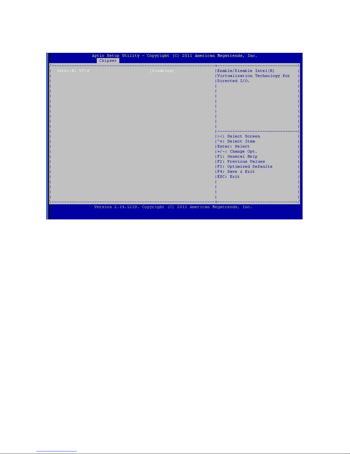
3.7.1.1.1 Intel
®
VT for Directed I/O Configuration Submenu
Intel
®
VT-d
Enable/Disable Intel
®
Virtualization Technology Directed I/O.
[Disabled] / [Enabled]
Default is [Disabled]
NOTE: The following items will appear when Intel
®
VT-d is set to [Enabled].
Interrupt Remapping
Enable/Disable VT-d Engine Interrupt Remapping Support.
[Enabled] / [Disabled]
Default is [Enabled]
Coherency Support
Enable/Disable VT-d Engine Coherency Support.
[Disabled] / [Enabled]
Default is [Disabled]
ATS Support
Enable/Disable VT-d Engine Address Translation Services support.
[Disabled] / [Enabled]
Default is [Disabled]
Page 79
79
Pass-through DMA
Enable/Disable VT-d Engine Pass through DMA support.
[Enabled] / [Disabled]
Default is [Enabled]
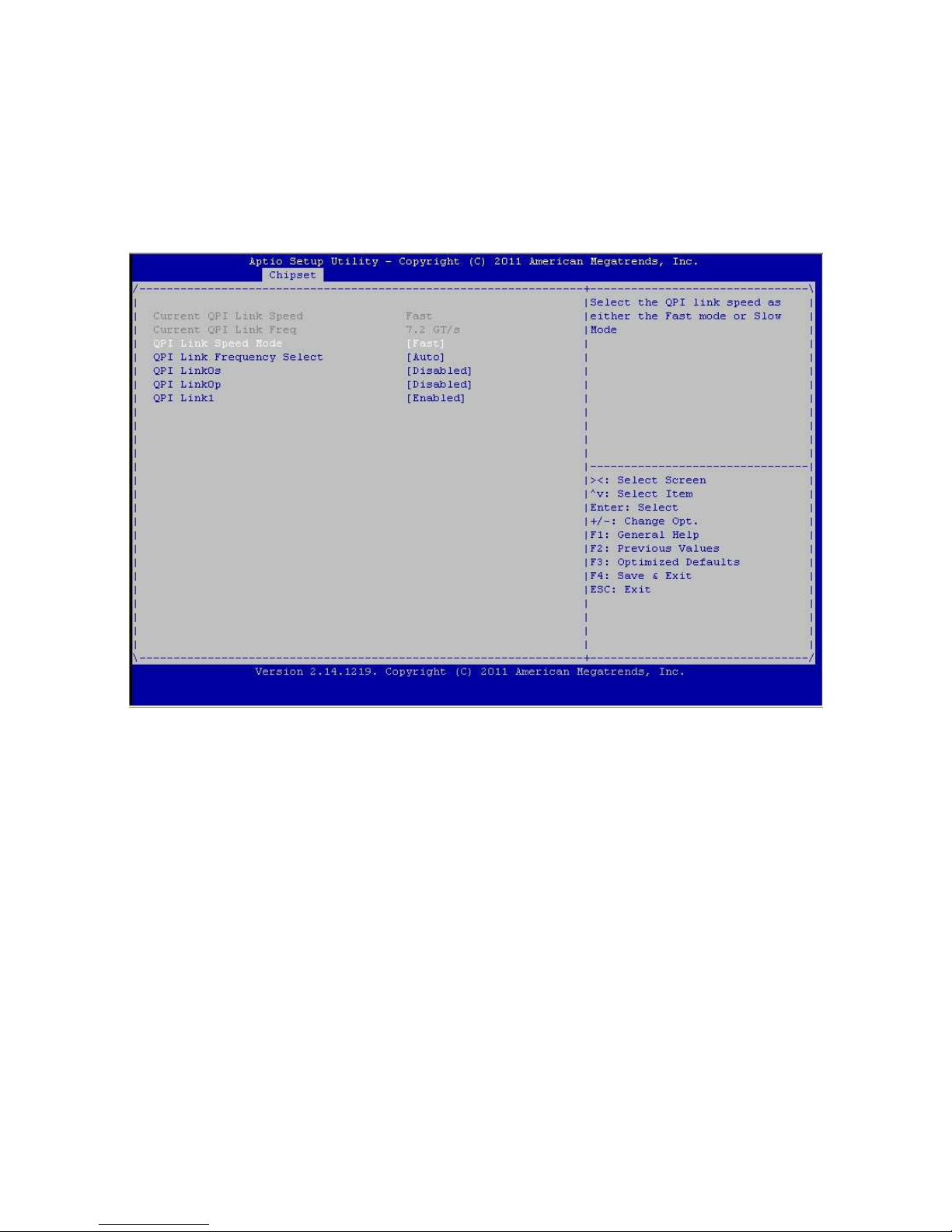
3.7.1.2 QPI Configuration Submenu
QPI Link Speed Mode
Select the QPI link speed as either the Fast Mode or the Slow Mode.
[Fast] / [Slow]
Default is [Fast]
QPI Link Frequency Select
Select the QPI Link Frequency.
[Auto] / [6.4GT/s] / [7.2GT/s] / [8.0GT/s]
Default is [Auto]
QPI LinkOs
Enable/Disable QPI LinkOs.
[Enabled] / [Disabled]
Default is [Disabled]
Page 80

80
QPI LinkOp
Enable/Disable QPI LinkOp.
[Enabled] / [Disabled]
Default is [Disabled]
QPI Link1
Enable/Disable QPI Link1.
[Enabled] / [Disabled]
Default is [Enabled]
Page 81
81
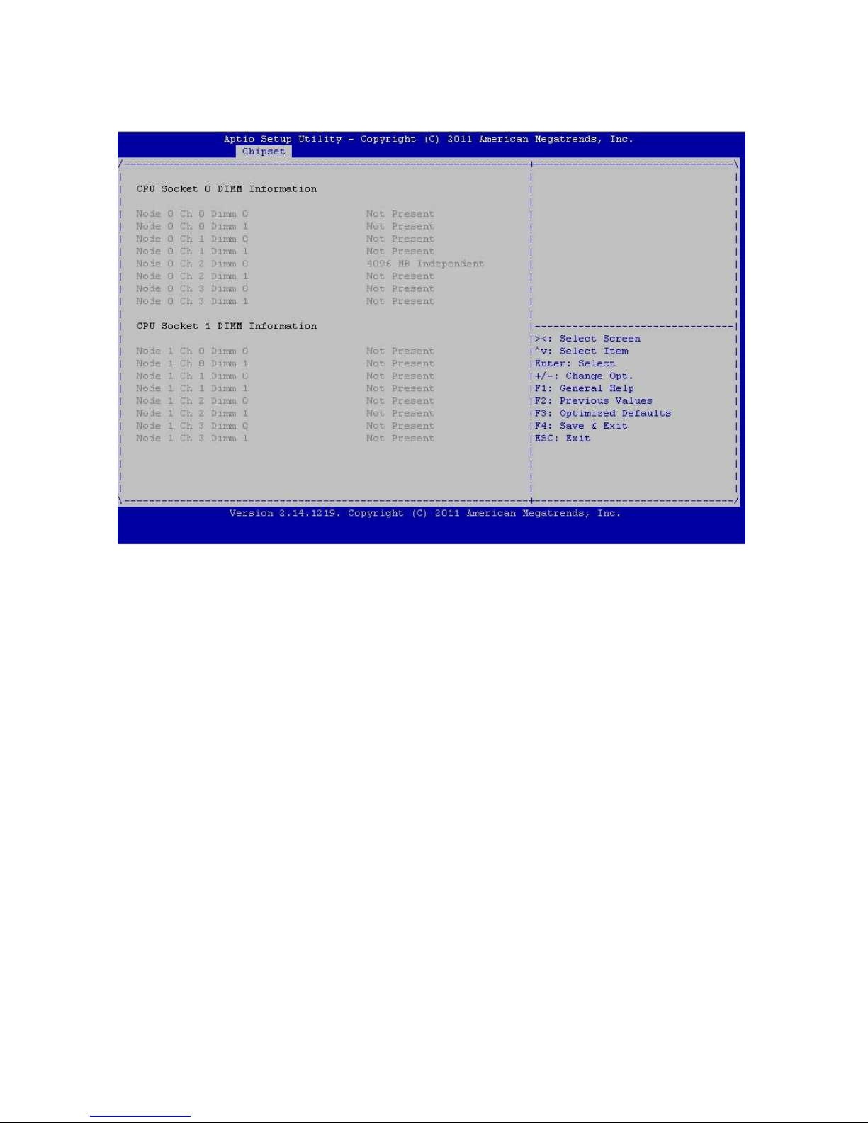
3.7.1.3 DIMM Information Submenu
Read only.
Page 82
82
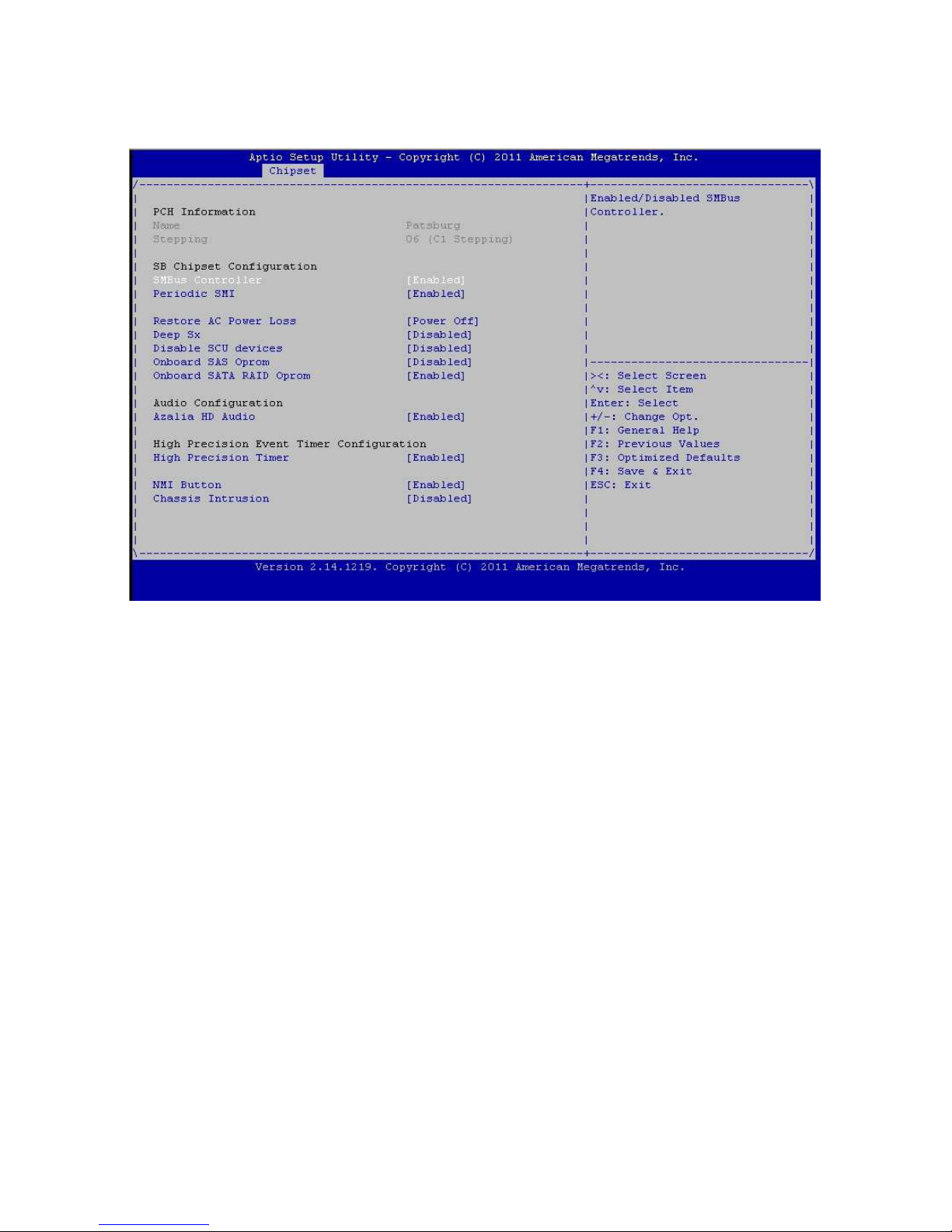
3.7.2 – South Bridge Configuration Sub-Menu
PCH Information
Name / Stepping
Only read
SMBus Controller
[Disabled] / [Enabled]
Default is [Enabled]
Periodic SMI
[Disabled] / [Enabled]
Default is [Enabled]
Restore AC Power Loss
[Power Off] / [ Power On]/[ Last State]
Default is [Power Off]
Deep Sx
Deep Sx configuration.
NOTE: Mobile platforms support Deep S4/S5 in DC only and Desktop platforms
support Deep S4/S5 in AC only.
Page 83

83
[Disabled] / [Enabled in S5 (Battery)] / [Enabled in S5] / [Enabled in S4 and S5
(Battery)] / [Enabled in S4 and S5]
Default is [Disabled]
Disable SCU devices
[Disabled] / [Enabled]
Default is [Disabled]
Onboard SAS OPROM
Enable/Disable onboard SAS RAID option rom if Launch Storage OpROM is
enabled.
[Enabled] / [Disabled]
Default is [Disabled]
Onboard SATA RAID OPROM
Enable/Disable onboard SATA RAID option rom if Launch Storage OpROM is
enabled.
[Enabled] / [Disabled]
Default is [Enabled]
Azalia HD Audio
[Enabled] / [Disabled]
Default is [Enabled]
Azalia internal HDMI
[Enabled] / [Disabled]
Default is [Disabled]
NMI Button
[Enabled] / [Disabled]
Default is [Enabled]
Chassis Intrusion
Enabled: When a chassis open event is detected, the BIOS will display the event.
[Enabled] / [Disabled]
Default is [Disabled]
Page 84
84
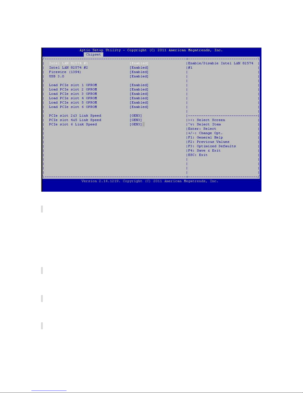
3.7.3 – Onboard Devices Configuration Sub-Menu
Intel LAN 82574 #1
[Enabled with iSCSI] / [Enabled with PXE] / [Enabled] / [Disabled]
Default is [Enabled]
Intel LAN 82574 #2
[Enabled with PXE] / [Enabled] / [Disabled]
Default is [Enabled]
Firewire(1394)
Enable/disable firewire(1394)
[Enabled] / [Disabled]
Default is [Enabled]
USB3.0
[Enabled] / [Disabled]
Default is [Enabled]
Load PCIe slot 1/2/3/4/5/6 OPROM
[Enabled] / [Disabled]
Default is [Enabled]
Page 85
85
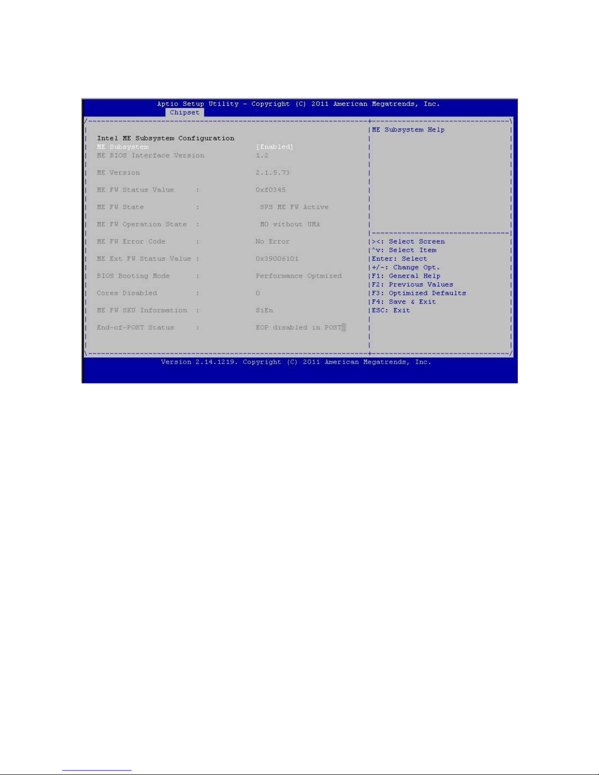
3.7.4 – ME Sub- Menu
ME Subsystem
Me subsystem Help
[Enabled] / [Disabled]
Default is [Enabled]
Page 86
86
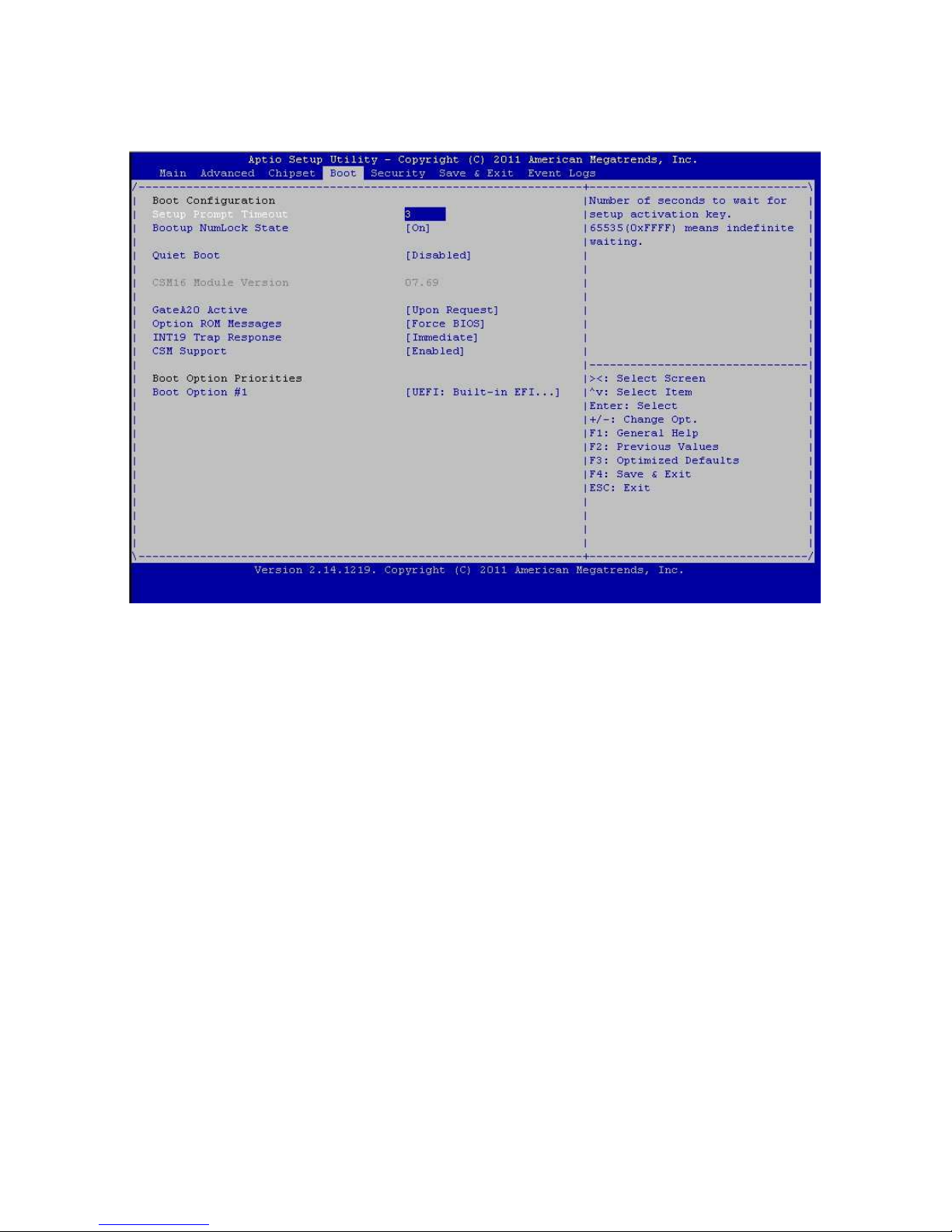
3.8 - Boot Configuration
Setup Prompt Timeout
Only read
Bootup Numlock State
Select the keyboard Numlock state
[On] / [Off]
Default is [On]
Quiet Boot
[Disabled] / [Enabled]
Default is [Disabled]
GateA20 Active
[Upon Request] / [Always]
Default is [Upon Request]
Option ROM Messages
Set display mode for option ROM upon request—GA20 can be disabled using BIOS
series Always—do not allow disabling GA20; this option is useful when any RT code
is executed above IMB.
[Force BIOS] / [Keep Current]
Default is [Force BIOS]
Page 87

87
INT 19 Trap Response
BIOS reaction on INT19 trapping by option ROM: IMMEDIATE-execute the trap
right away; POSTPONED-execute the trap during legacy boot.
[Immediate] / [Postponed]
Default is [Immediate]
Boot Option #1
Select the first boot device.
[Device Name] / [Disabled]
Default is [Device Name]
Page 88
88
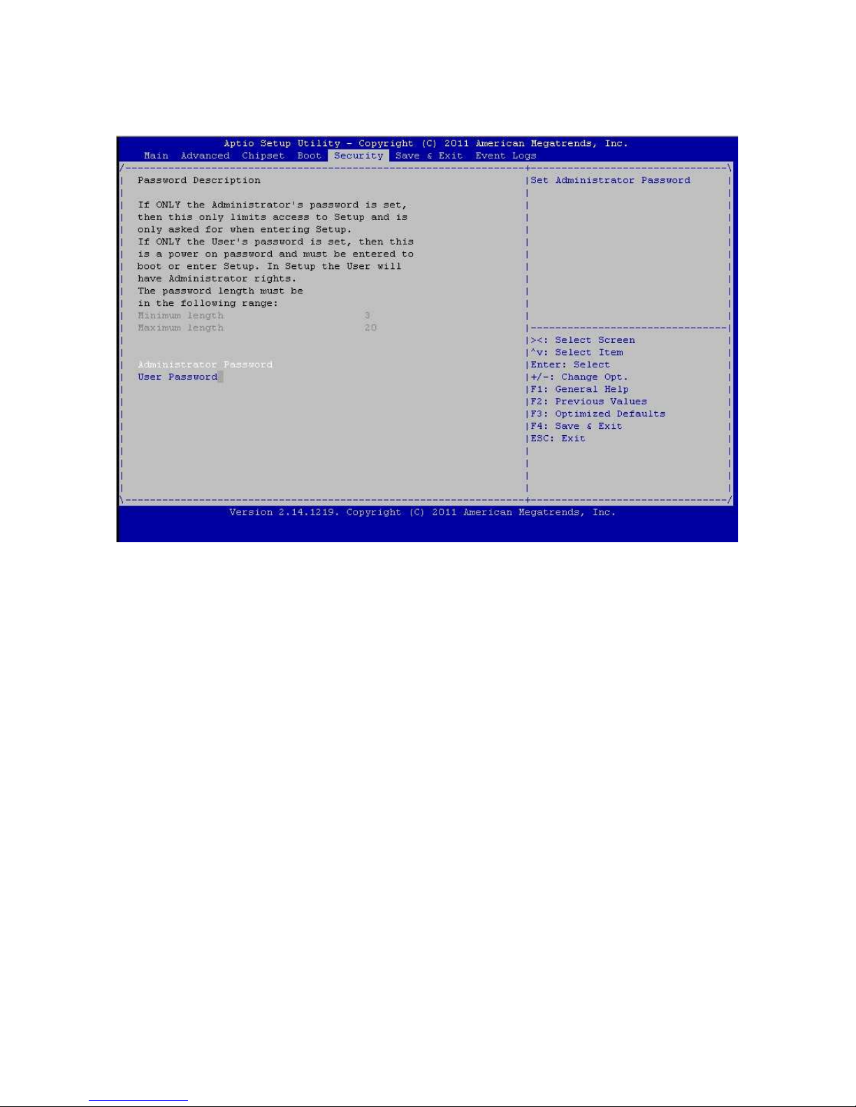
3.9 - Security Menu
Password Description
Read only.
Administrator Password
Install or change the password.
User Password
Install or change the password.
Page 89
89
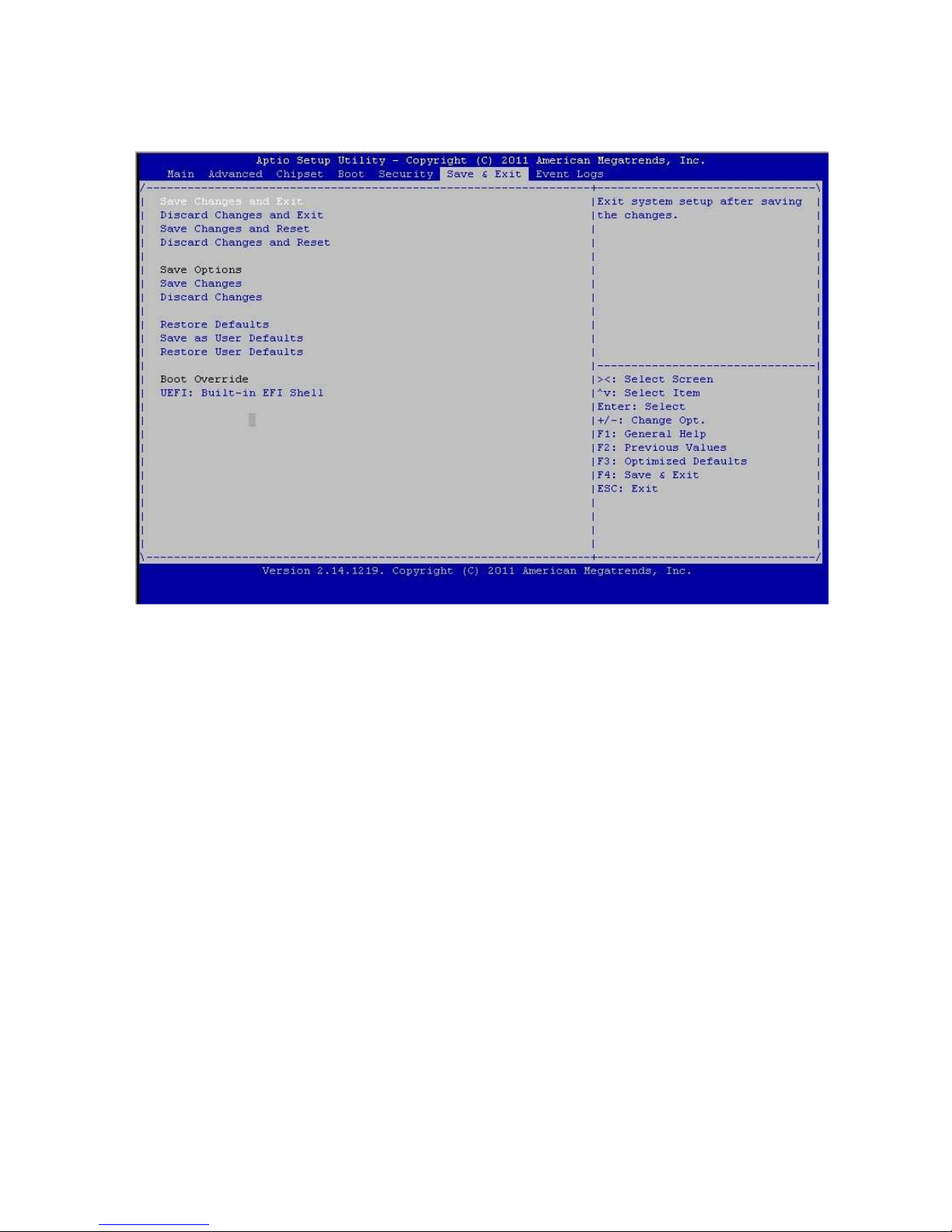
3.10 - Save & Exit Menu
Save Changes and Exit
Use this option to exit setup utility and re-boot.
All new selections you have made are stored into CMOS.
System will use the new settings to boot up.
Discard Changes and Exit
Use this option to exit setup utility and re-boot.
All new selections you have made are not stored into CMOS.
System will use the old settings to boot up.
Save Changes and Reset
Use this option to save all new setup values that you have made and reset.
Discard Changes and Reset
Use this option to discard all new setup values that you have made and
reset.
Save Changes
Use this option to save all new setup values that you have made
Discard Changes
Use this option to load all default failsafe setup values.
Page 90

90
Restore Defaults
Use this option to restore defaults
Save as user Defaults
Use this option to save the user defaults
Restore user Defaults
Use this option to restore the user defaults.
Page 91
91
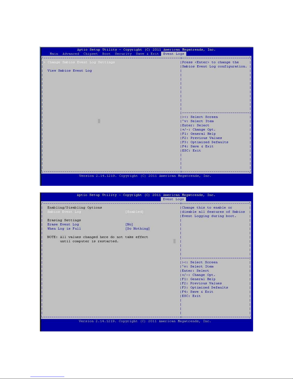
3.11 - Event Logs
Page 92

92
Smbios Event Log
Change this to enable or disable all features of Smbios Event Logging during boot.
[Enabled] / [Disabled]
Default is [Enabled]
Erase Event Log
Choose options for erasing Smbios Event Log. Erasing is done prior to any logging
activation during reset.
[NO] / [Yes,next year] / [Yes, every year]
Default is [NO]
When Log is full
Choose options for reactions to a full Smbios Event Log.
[Do Nothing] / [Erase Immediately]
Default is [Do Nothing]
Page 93

93
Chapter 4: Diagnostics
If you experience problems with setting up your system, always check the
following things in the following order:
Memory, Video, CPU
By checking these items, you will most likely find out what the problem might
have been when setting up your system. For more information on
troubleshooting, check the Leadtek website at: http://www.leadtek.com.
4.1 - Flash Utility
Every BIOS file is unique for the motherboard it was designed for. For Flash
Utilities, BIOS downloads, and information on how to properly use the Flash
Utility with your motherboard, please check the Leadtek web site:
http://www.leadtek.com/
NOTE: Please be aware that by flashing your BIOS, you agree that in the
event of a BIOS flash failure, you must contact your dealer for a
replacement BIOS. There are no exceptions. Leadtek does not have a
policy for replacing BIOS chips directly with end users. In no event will
Leadtek be held responsible for damages done by the end user.
Page 94

94
4.2 - AMIBIOS Post Code (Aptio)
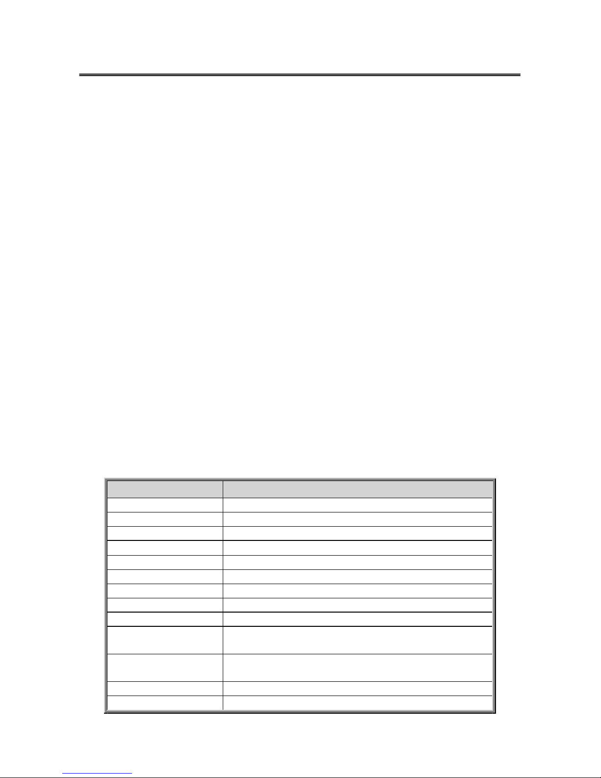
The POST code checkpoints are the largest set of checkpoints during the BIOS preboot process. The following table describes the type of checkpoints that may occur
during the POST portion of the BIOS:
Checkpoint Ranges
Status Code Range
Description
0x01 – 0x0B
SEC execution
0x0C – 0x0F
Sec errors
0x10 – 0x2F
PEI execution up to and including memory detection
0x30 – 0x4F
PEI execution after memory detection
0x50 – 0x5F
PEI errors
0x60 – 0x8F
DXE execution up to BDS
0x90 – 0xCF
BDS execution
0xD0 – 0xDF
DXE errors
0xE0 – 0xE8
S3 Resume (PEI)
0xE9 – 0xEF
S3 Resume errors (PEI)
0xF0 – 0xF8
Recovery (PEI)
0xF9 – 0xFF
Recovery errors (PEI)
Standard Checkpoints
SEC Phase
Status Code Description
0x00
Note used
Progress Codes
0x01
Power on. Reset type detection (soft/hard).
0x02
AP initialization before microcode loading
0x03
North Bridge initialization before microcode loading
0x04
South Bridge initialization before microcode loading
0x05
OEM initialization before microcode loading
0x06
Microcode loading
0x07
AP initialization after microcode loading
0x08
North Bridge initialization after microcode loading
0x09
South Bridge initialization after microcode loading
0x0A
OEM initialization after microcode loading
0x0B
Cache initialization
Page 95

95
SEC Error Codes
0x0C – 0x0D Reserved for future AMI SEC error codes
0x0E
Microcode not found
0x0F
Microcode not found
SEC Beep Codes
None
PEI Phase
Status Code Description
Progress Codes
0x10
PCI Core is started
0x11
Pre-memory CPU initialization is started
0x12
Pre-memory CPU initialization (CPU module specific)
0x13
Pre-memory CPU initialization (CPU module specific)
0x14
Pre-memory CPU initialization (CPU module specific)
0x15
Pre-memory North Bridge initialization is started
0x16
Pre-Memory North Bridge initialization (North Bridge module specific)
0x17
Pre-memory North Bridge initialization (North Bridge module specific)
0x18
Pre-Memory North Bridge initialization (North Bridge module specific)
0x19
Pre-memory South Bridge initialization is started
0x1A
Pre-Memory South Bridge initialization (South Bridge module specific)
0x1B
Pre-memory South Bridge initialization (South Bridge module specific)
0x1C
Pre-Memory South Bridge initialization (South Bridge module specific)
0x1D – 0x2A
OEM pre-memory initialization codes
0x2B
Memory initialization. Serial Presence Detect (SPD) data reading
0x2C
Memory initialization. Memory presence detection
0x2D
Memory initialization. Programming memory timing information
0x2E
Memory initialization. Configuring memory
0x2F
Memory initialization (other)
0x30
Reserved for ASL (see ASL Status Codes section below)
0x31
Memory Installed
0x32
CPU post-memory initialization is started.
0x33
CPU post-memory initialization. Cache initialization
0x34
CPU post-memory initialization. Application Processor(s) (AP) initialization
0x35
CPU post-memory initialization. Boot Strap Processor (BSP) selection
0x36
CPU post-memory initialization. System Management Mode(SMM) initialization
0x37
Post-Memory North Bridge initialization is started.
Page 96

96
Status Code Description
0x38
Post-Memory North Bridge initialization (North Bridge module specific)
0x39
Post-Memory North Bridge initialization (North Bridge module specific)
0x3A
Post-Memory North Bridge initialization (North Bridge module specific)
0x3B
Post-Memory South Bridge initialization is started
0x3C
Post-Memory South Bridge initialization (South Bridge module specific)
0x3D
Post-Memory South Bridge initialization (South Bridge module specific)
0x3E
Post-Memory South Bridge initialization (South Bridge module specific)
0x3F – 0x4E OEM post memory initialization codes
0x4F
DXE PIL is started
PCI Error Codes
0x50
Memory initialization error. Invalid memory type or incompatible memory speed
0x51
Memory initialization error. SPD reading has failed.
0x52
Memory initialization error. Invalid memory size or memory modules do not match.
0x53
Memory initialization error. No usable memory detected
0x54
Unspecified memory initialization error
0x55
Memory not installed
0x56
Invalid CPU type or speed
0x57
CPU mismatch
0x58
CPU self test failed or possible CPU cache error
0x59
CPU microcode is not found or microcode update is failed.
0x5A
Internal CPU error
0x5B
Reset PPI is not available.
0x5C – 0x5F Reserved for future AMI error codes
S3 Resume Progress Codes
0xE0
S3 Resume is started (S3 Resume PPI is called by the DXE IPL).
0xE1
S3 Boot Script execution
0xE2
Video repost
0xE3
OS S3 wake vector call
0xE4 – 0xE7 Reserved for future AMI progress codes
S3 Resume Error Codes
0xE8
S3 Resume failed
0xE9
S3 Resume PPI not found
0xEA
S3 Resume Boot Script error
0xEB
S3 OS wake error
0xEC – 0xEF Reserved for future AMI error codes
Page 97

97
Recovery Progress Codes
0xF0
Recovery condition triggered by firmware (Auto recovery)
0xF1
Recovery condition triggered by user (forced recovery)
0xF2
Recovery process started
0xF3
Recovery firmware image is found.
0xF4
Recovery firmware image is loaded.
0xF5 – 0xF7
Reserved for future AMI progress codes
Recovery Error Codes
0xF8
Recovery PPI is not available.
0xF9
Recovery capsule is not found.
0xFA
Invalid recovery capsule
0xFB – 0xFF Reserved for future AMI error codes
PEI Beep Codes
# of Beeps
Description
1 (repeatedly) Memory not installed
1
Memory was installed twice (installPEIMemory routine in PEI Core called twice).
2
Recovery started
3
DXEIPL was not found.
3
DXE Core Firmware Volume was not found.
4
Recovery failed
4
S3 Resume failed
7
Reset PPI is not available.
DXE Phase
Status Code Description
0x60
DXE Core is started.
0x61
NVRAM initialization
0x62
Installation of the South Bridge Runtime Services
0x63
CPU DXE initialization is started.
0x64
CPU DXE initialization (CPU module specific)
0x65
CPU DXE initialization (CPU module specific)
0x66
CPU DXE initialization (CPU module specific)
0x67
CPU DXE initialization (CPU module specific)
0x68
PCI host bridge initialization
0x69
North Bridge DXE initialization is started.
0x6A
North Bridge DXE SMM initialization is started.
Page 98

98
Status Code Description
0x6B
North Bridge DXE initialization (North Bridge module specific)
0x6C
North Bridge DXE initialization (North Bridge module specific)
0x6D
North Bridge DXE initialization (North Bridge module specific)
0x6E
North Bridge DXE initialization (North Bridge module specific)
0x6F
North Bridge DXE initialization (North Bridge module specific)
0x70
South Bridge DXE initialization is started.
0x71
South Bridge DXE SMM initialization is started.
0x72
South Bridge devices initialization
0x73
South Bridge DXE initialization (South Bridge module specific)
0x74
South Bridge DXE initialization (South Bridge module specific)
0x75
South Bridge DXE initialization (South Bridge module specific)
0x76
South Bridge DXE initialization (South Bridge module specific)
0x77
South Bridge DXE initialization (South Bridge module specific)
0x78
ACPI module initialization
0x79
CSM initialization
0x7A – 0x7F Reserved for future AMI DXE codes
0x80 – 0x8F
OEM DXE initialization codes
0x90
Boot Device Selection (BDS) phase is started
0x91
Driver connecting is started
0x92
PCI Bus initialization is started
0x93
PCI Bus Hot Plug Controller initialization
0x94
PCI Bus Enumeration
0x95
PCI BUS Request Resources
0x96
PCI Bus Assign Resources
0x97
Console output devices connect
0x98
Console Input devices connect
0x99
Super IO initialization
0x9A
USB initialization is started.
0x9B
USB Reset
0x9C
USB Detect
0x9D
USB Enable
0x9E -0x9F
Reserved for future AMI codes
0xA0
IDE initialization is started
0xA1
IDE Reset
0xA2
IDE Detect
Page 99

99
Status Code Description
0xA3
IDE Enable
0xA4
SCSI initialization is started.
0xA5
SCSI Reset
0xA6
SCSI Detect
0xA7
SCSI Enable
0xA8
Setup Verifying Password
0xA9
Start of Setup
0xAA
Reserved for ASL (see ASL Status Codes section below)
0xAB
Setup Input Wait
0xAC
Reserved for ASL (see ASL Status Codes section below)
0xAD
Ready To Boot event
0xAE
Legacy Boot event
0xAF
Exit Boot Services event
0xB0
Runtime Set Virtual Address MAP Begin
0xB1
Runtime Set Virtual Address MAP End
0xB2
Legacy Option ROM initialization
0xB3
System Reset
0xB4
USB hot plug
0xB5
PCI bus hot plug
0xB6
Clean-up of NVRAM
0xB7
Configuration Reset (reset of NVRAM settings)
0xB8 – 0xBF
Reserved for future AMI codes
0xC0 – 0xCF OEM BDS initialization codes
DXE Error Codes
0xD0
CPU initialization error
0xD1
North Bridge initialization error
0xD2
South Bridge initialization error
0xD3
Some of the Architectural Protocols are not available
0xD4
PCI resource allocation error. Out of Resources
0xD5
No Space for Legacy Option ROM
0xD6
No Console Output Devices are found.
0xD7
No Console Input Devices are found.
0xD8
Invalid password
0xD9
Error loading Boot Option (LoadImage returned error)
0xDA
Boot Option is failed (StartImage returned error).
Page 100

100
Status Code Description
0xDB
Flash update is failed.
0xDC
Reset protocol is not available.
DXE Beep Codes
# of Beeps
Description
1
Invalid password
4
Some of the Architectural Protocols are not available.
5
No Console Output Devices are found.
5
No Console Input Devices are found.
6
Flash update is failed.
7
Reset protocol is not available.
8
Platform PCI resource requirements cannot be met.
ACPI/ASL Checkpoints
Status Code Description
0x01
System is entering S1 sleep state.
0x02
System is entering S2 sleep state.
0x03
System is entering S3 sleep state.
0x04
System is entering S4 sleep state.
0x05
System is entering S5 sleep state.
0x10
System is waking up from the S1 sleep state.
0x20
System is waking up from the S2 sleep state.
0x30
System is waking up from the S3 sleep state.
0x40
System is waking up from the S4 sleep state.
0xAC
System has transitioned into ACPI mode. Interrupt controller is in APIC mode.
0xAA
System has transitioned into ACPI mode. Interrupt controller is in APIC mode.
 Loading...