

LDT Littfinski Daten Technik RM-88-N-O-B Operation Instruction
Littfinski DatenTechnik (LDT)
Pos.
Qty.
Component
Remarks
Ref.
Done
Assembly Instruction
16-fold Feedback Module
for the s88-Feedback bus
from the Digital-Professional-Series!
RM-88-N-O-B Part-No.: 310101
As Märklin s88 with 16 opto-coupling inputs.
Suitable for digital control devices and interfaces
with s88-feedback bus:
⇒ with 16 opto-coupling input connections
(for potential separation and high interference protection e.g. for
contact tracks [one isolated rail], switch tracks reed-contacts or
turnout feedback report).
⇒ for s88-standard connections and s88-N
(with 6-poles s88-pinbars and RJ-45 sockets).
⇒ suitable for the digital control:
Märklin-Digital~/=,Central Station 1 and 2, Intellibox, TWINCENTER, HSI-88(-USB), EasyControl, ECoS, DiCoStation.
This product is not a toy! Not suitable for children under 14 years of age! The kit
contains small parts, which should be kept away from children under 3! Improper
use will imply danger or injuring due to sharp edges and tips! Please store this
instruction carefully.
CE Part.-No.:
24 80 33
s88-N
Introduction:
You have purchased the 16-fold Feedback Module RM-88-N-O
as a kit for your model railway. The RM-88-N-O is a high
quality product that is supplied within the assortment of
Littfinski DatenTechnik (LDT).
The Feedback Module RM-88-N-O from the Digital-
Professional-Series can operate on your digital control without
any problems.
The RM-88-N-O is suitable for the application on any digital
control unit which supports the s88 feedback bus
We are wishing that you will have a good time for assembling
and using this product.
General:
Tools required for the assembly
Please assure that the following tools are available:
• a small side cutter
• a mini soldering iron with a small tip
• solder tin (if possible 0,5mm diameter)
Safety Instructions
• All electrical and electronic components included in this kit
shall be used on low voltage only by using a tested and
approved voltage transducer (transformer). All components
are sensitive to heat. During soldering the heat shall be
applied to the respective component for a very short period
only.
• The soldering iron develops up to 400°C. Please keep
continual attention to this tool. Keep sufficient distance to
combustible material. Use a heat resistant pad for this work.
>> kit <<
• This kit consist of small parts, which can be possibly
swallowed from children. Children (especially under 3 years)
shall not participate on the assembly without supervision.
Set-Up:
For the board assembly please follow exact the sequence of
the below assembly list. Cross each line off as done after
completing the insertion and the soldering of the respective
part.
Please put the clamps together to a block with 17 connections
before assembling the clamps to the board.
Special attention is required for the tantalum capacitor. The
leg with the mark "+" has to be inserted to the respective
marked position on the pc-board.
Resistor-networks are marked on one end with a printed
circle or a square. Assemble this component that way that the
marking corresponds with the marking between the first and
second bore on the pc-board. The first bore has been
additionally marked with a "1".
Please attend to the flat side of the transistor.
Integrated circuits (IC`s) are either marked with a half round
notch on one end or a printed point for the correct mounting
position. Push the IC`s into the correct socket assuring that the
notch or the printed point is corresponding to the half-rounded
marking on the pc-board.
Please attend to the sensitivity of the ICs to electrostatic
discharge, which will cause immediate damage of the IC.
Before touching those components please discharge yourself
by contacting an earthed metal ( e.g. earthed radiator) or work
with an electrostatic safety pad.
Please glue the two labels onto the RJ-45 sockets for
identification of the output socket BU1 (cable in direction to the
central unit) and BU2 (cable from next feedback unit).
s88-N
OUT
s88-N
Label for BU1 Label for BU2
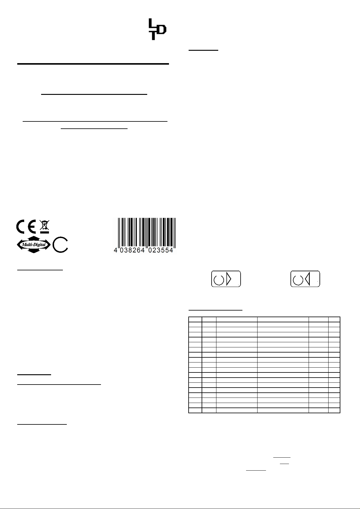
Assembly List:
1 1 Printed Circuit Board
2 10 IC-Sockets 16poles IC1..6
3 4 Networks 4*10kOhm Attend to the polarity! R1..R4
4 2 Networks 8*22kOhm Attend to the polarity! R5, R6
5 2 Resistors 100kOhm brown-black-black-orange R7, R8
6 1 Resistor 10kOhm brown-black-black-red R9
7 16 Capacitors 10nF C1..C16
8 1 Tantalum cap. 1uF/35V Attend to the polarity! C17
9 1 Capacitor 100nF C18
10 2 Pin-plugs 6poles ST1, ST2
11 1 Transistor BC 547 Attend to the polarity! T1
12 5 Clamps 3poles Build a block before assy.! KL1..KL5
13 1 Clamp 2poles Build a block with KL1 to 5 KL6
14 2 RJ45 sockets BU1, BU2
15 4 IC: 4044 Attend to the polarity! IC1,2,4,5
16 2 IC: 4014 Attend to the polarity! IC3, IC6
17 4 IC: 844 Attend to the polarity! IC7…10
18 Final Control
Made in Europe by
Littfinski DatenTechnik (LDT)
Kleiner Ring 9
D-25492 Heist/Germany
Phone: 0049 4122 / 977 381
Fax: 0049 4122 / 977 382
Subject to technical changes and errors. 05/2013 by LDT
Internet: http://www.ldt-infocenter.com
Märklin is a registered trade mark.
IN

Soldering instruction
Provided you have no special experience in soldering electronic
components please read first this soldering instruction before starting the
job. Soldering has to be trained!
1. Never use additional fluxes for soldering electronic circuits which
contain acids (e.g. zinc chloride or ammonium chloride). Those can
destroy components and printed circuits when not washed off
completely.
2. As soldering material only lead free soldering tin with a rosin core for
fluxing should be used.
3. Use a small soldering iron with max 30 Watt heating power. The solder
tip shall be free from scale to assure an excellent heat transfer to the
area to be soldered.
4. The soldering shall be performed on a speedy way because a long
heat transfer can destroy the components. To much or to long heating
can take off the copper pads and copper tracks from the board.
5. For a good soldering a well tinned solder-tip has to be brought in
contact to the copper-pad and the component wire at the same time.
Simultaneous a little solder-tin shall be applied for heating up. As soon
as the solder-tin starts melting the tin wire has to be taken away. Just
wait until the tin has well wetted the pad and the wire and take the
soldering iron away from the soldering area.
6. Make sure not to move the just soldered component for about 5
seconds after removing the soldering iron. This should create a silver
shining faultless soldering joint.
7. For a faultless soldering joint and well done soldering is a clean non oxidized soldering-tip absolutely required. It is not possible to perform
a sufficient soldering joint with a dirty soldering tip. Therefore please
clean the soldering tip from excessive solder-tin and dirt by using a wet
sponge or a silicone cleaning pad after each soldering process.
8. After completion of the soldering all connection wires have to be cutted
off directly above the soldering joint by using a side cutter.
9. By soldering semiconductors (transistors, diodes), LED`s and IC`s is
it very important never to exceed the soldering time of 5 seconds to
prevent the destruction of the component. It is absolutely required to
attend to the correct polarity of the component before starting the
soldering process.
10. After the board assembly carefully control the pc-board about correct
insertion of the components and the correct polarity. Please check if
no connections or copper tracks are accidentally short circuited by
soldering tin. This can not only result to malfunction of the module but
also result to a destruction of expensive components.
11. Please take into account that improper soldering joints, wrong
connections, faulty operation or wrong board assembly is not a matter
within our sphere of influence.
General installation information
The contact-wires of resistors and diodes to be assembled in a lying
position shall be bended in accordance to the raster distance into a right
angular position and assembled into the specified bores (in accordance to
the board assembly plan or the assembly markings). To prevent that the
components will not fall out by turn-over the pc-board please bend the
connection wires about 45° apart and solder them carefully to the copper
pads on the rear side of the board. Finally the excessive wires shall be
cutted off with a small side cutter.
The resistors in the supplied kits are metal-foil resistors. Those have a
tolerance of 1% and are marked with a brown “tolerance-ring”. The
tolerance ring can be identified by the larger margin distance respectively
the larger distance to the other four marking rings. Normally there are five
color rings on the metal-foil resistors. To read the color code you have to
locate the resistor that way that the brown tolerance ring will be on the right
side. The color rings will be red now from left to right!
Please take care to assemble diodes with the correct polarity (position of
the cathode marking). Take care about a very short soldering time! The
same will apply to the transistors and the integrated circuits (IC`s). The flat
side of the transistors has to correspond with the marking on the pc-board.
The transistor legs should never be assembled in a crossed position.
Further those components should have a distance of about 5mm to the
board. Attend to the short soldering time to prevent the damage of the
component by excessive heat.
Capacitors shall be assembled into the respective marked bores, the wires
to be bent a little apart and careful soldered to the copper pad. By the
assembly of electrolytic capacitors (electrolytic cap) it has to be attended to
the correct polarity (+,-)! Wrong-way soldered electrolytic capacitors
can explode during the application! Therefore is it very important to
check the correct polarity two- or even better three-times. In addition it has
to be attended to the correct capacitor values, e.g. n10 = 100pF (not
10nF!).
A careful and clean assembly will drastically reduce the possibility that
anything will not be in correct function. Check every step and every
soldering joint two times before carrying on! Attend closely to the assembly
list! Perform the described step not different and do not skip any step!
Mark each step as done at the foreseen column after assembly and careful
check.
Take your time. Private work is no piece-work because the time for careful
assembly work is much less than an extensive fault diagnosis.
Final assembly
Sockets and integrated circuits (IC´s) of the kits will be supplied on a piece
of foam to assure safe transport.
This foam shall never be used below or between components as this foam
is electrical conductive.
In case the kit will be taken into operation the conductive foam can produce
a short circuitry and destroy the complete kit. Anyhow the function of the
module will not be as expected.
Warranty
As we have no influence to the proper and correct assembly we have to
limit our warranty to the complete supply and the faultless quality of the
components.
We guarantee the function of the components in accordance to the
identified values within a non-assembled condition of the parts and the
compliance of the technical data of the circuit by attending to the
respective soldering instruction and the specified start of operation of the
module including connection and operation.
Further demands are not accepted.
We are not taking over any warranty nor any liability for any harm or
sequential damage connected to this product.
We reserve our right for a repair, rework, supply of replacement or refund
of the purchase price.
The following criteria will result to a non-repair respectively to a lost of right
to claim under guarantee:
• if acid-containing soldering tin or fluxes with corrosive content and
others have been used
• if the kit has been improper soldered or assembled
• by alterations or repair-trials on the device
• by own circuit amendments
• by construction of non-intended improper displacement of
components, free wiring of components etc.
• application of other non-original kit-components
• by damaging of copper tracks or soldering copper pads on the board
• by wrong assembly and the sub sequential damages
• overloading the module
• by damages caused by intervention of foreign persons
• by damages caused by disregarding the operation manual respectively
the connection plan
• by connecting a wrong voltage respectively a wrong current
• by wrong polarity connection of the module
• by wrong operation or damages caused by negligent usage or abuse
• by defects caused by bridged or wrong fuses.
All such cases will result to a return of the kit to your expenses.
Subject to technical changes and errors. 05/2013 by LDT
 Loading...