

LDIC LD3500 Datasheet

LD3500-XX
1 up to 4 Channel
+5V GMR Head Preamplifier
FEATURES
• Current Bias/Current Sense Architecture
• Operates from 5V supply
• Variable Power Supply from 5 to 8V for
Writer High Performance Circuitry (Patent
Pending)
• 3-line serial interface with readback (3.3V
CMOS compatible)
• Power management modes
• On-chip temperature monitor
• Internal reference resistor (2Kohm)
(External optional)
• Head unsafe fault detection for both read
and write
• Unselected read/write heads at GND
potential
• Fast recovery mode
• 300MHz Read Bandwidth
• One side grounded input, fully differential
output
• Read frequency boost
• Programmable GMR resistance
measurement mode (5-bits)
• Programmable GMR Pinned Layer Reset
(PLR) pulse circuit
• GMR bias current range 2-9.75 mA (5-bits)
• GMR resistor range = 25 to 75 Ω
• Programmable read gain = 225 V/V or 300
V/V
• Input equivalent noise TBD nV√Hz @ Rmr
= 45Ω
• TA detection & programmable
compensation
• 1.7ns Write rise/fall time (L=90 nH/40 mA)
• Variable Power Supply from 5 to 8V for
high performance Writer Circuitry up to
Rise/Fall Time: 0.5 ns Typical (Iw = 40 mA
(0-p), Ltf = 60 nH, Rtf = 15 Ω)
• Write current range = 15-60 mA (5-bits)
• Programmable write current overshoot (4-
bits)
• Programmable write current undershoot (3bit)
• 200ns Write/Read switching time
• Servo write (half bank or all bank write)
version 1.0
LD3500-XX
1 up to 4-Channel
+5V GMR Head Preamplifier
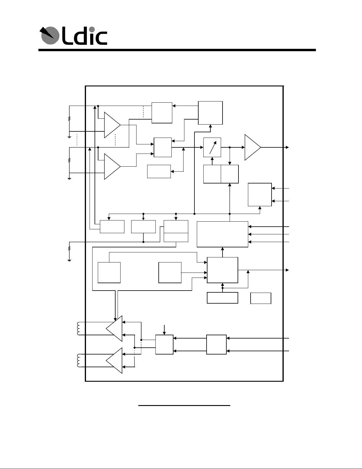
R0X
RnX
I
I
PLR/
MUX
VCC
Fault
Read
Bias
Head
Select
MUX
Sense
Head
MUX
Sense
Dummy
Head
A/V
TAC TAD
Buffer
Mode
Control
MRbias
DAC
Write
DAC
MUX
Temp
Serial Interface
&
Reg.
Fault
RDX/
RDY
MRRB
RBW
SDEN
SCLK
SDATA
FLT/BHV
Mon.
W0X
W0Y
WnX
WnY
BHV
From
H.S.
Write
Driver
WDI
MUX
Write
Driver
WDI
Vref
WDX
WDY
LD3500 Block Diagram
LDIC Confidential version 1.0
 Loading...