

LDIC LD3300-6, LD3300-4, LD3300-2, LD3300-16, LD3300-12 Datasheet
...
LD3300-XX
2, 4, 6, 8, 10, 12, 14, and 16-Channel Programmable
+5V, -3V, MR Head Preamplifier
r
version 3.0
DESCRIPTION
The LD3300-XX is one in the family of integrated
circuit products designed for use with MagnetoResistive recording heads. It is a register-based design
to provide maximum programmability. These devices
support 2, 4, 6, 8, 10 up to 16 channel MR Head. It
contains an MR low noise read amplifier, a thin film
head write driver and Interface/Command Control
block which provides the ability to program the
multiple operation modes, write currents and MR bias
voltages as well as control diagnostic functions. This
product family requires dual supply voltage of 5V, and
-3V. These devices are available in TQFP, or flip chip.
FEATURES
• Programmable Bandwidth from 150 to 360MHz
• Write current rise/fall time = 2.0ns
• Programmable Read Amplifier Gain 150, 250,
300, 350 V/V through ICCB (serial port)
• Programmable Thermal Asperity Threshold
Detection and Correction
• MR Head: Differential Voltage sense, Voltage
bias
• Head Unsafe, including Read and Write unsafe
sensing
• Interface/Command Control Block (ICCB) with
shadow register
• Servo write capability
• Power supply fault protection
• Programmable write current and MR bias voltage
• Available in TQFP & Flip Chip
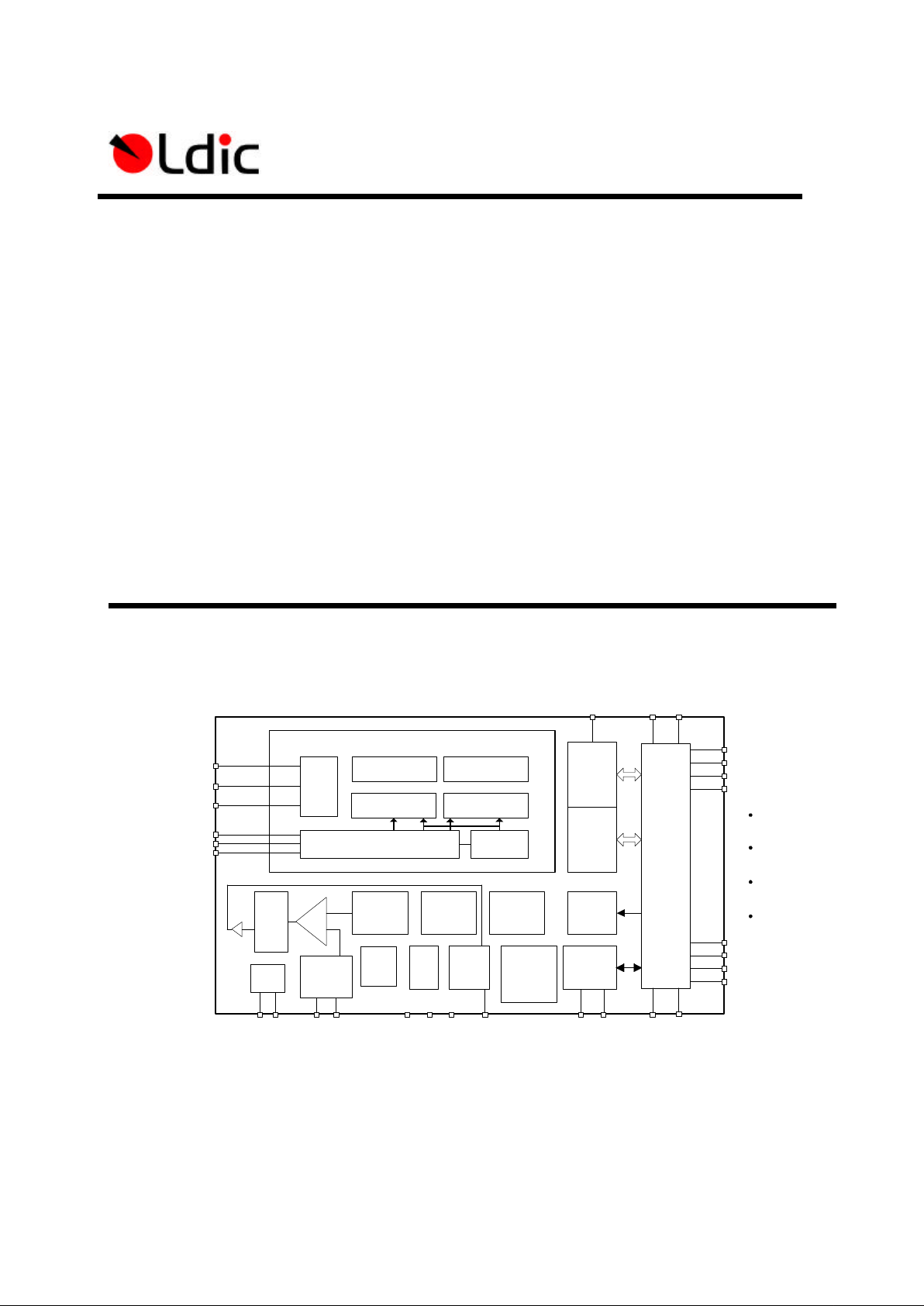
BLOCK DIAGRAM
Write
DAC
Read
DAC
Head
Unsafe
Write
Current
Bias
Vref
Current
Generator
POR
0.40
Multiplier
Read
Bias
Source
MUX
Write
Data
Serial Port Control
address
Decoder
Head
Select
Mode
Select
Write Register
Read Register
6 Channel R/W, MR Bias
Write Driver
Dummy
Head
Prog.
Gain
Post Pre
Amplifier
Read
Amp
Interface/Command Control Block
WDY
CN VEER
VEE VDD VSS
HUS
RDX RDY CBY1 CBX1
HRX0
HRY0
HWX0
HWY0
HRX5
HRY5
HWX5
HWY5
SDATA
SCLK
SDEN
MRRN
IWRN
CHEN
RREF CBY2 CBX2
WDX
Prog
Thermal
Asp. Detc.
&
Correction
LD3300-XX
2, 4, 6, 8, 10, 12, 14, and 16-Channel Programmable
+5V, -3V, MR Head Preamplifier
Page 19 version 3.0
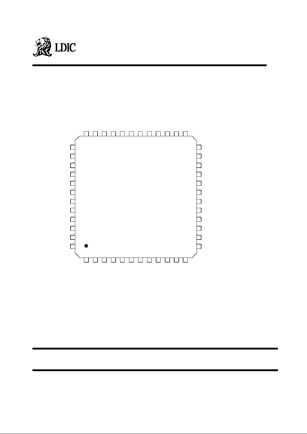
Figure 4 : TQFP 48 Package
This document may contain preliminary information and is subject to change by LDIC without notice. LDIC assumes no responsibility or liability for any use of this information herein. Nothing in this
document shall operate as an express or implied license of indemnity under the intellectual property rights of LDIC or third parties. NO WARRENTIES OF ANY KIND, INCLUDING, BUT NOT
LIMITED TO, THE IMPLIES WARRENTIES OF MERCHANTABILITY OR FITNESS FOR A PARTICULAR PURPOSE, ARE OFFERED IN THIS DOCUMENT.
7 8 9 10 11 12
13
14
16
15
17
20
18
19
21
22
23
24
1 2 3 4 5 6
30 29 28 27 26 2536 35 34 33 32 31
48
47
45
46
44
41
43
42
40
39
38
37
HWX0
HWY0
HRX0
HRY0
CBX1
CBY1
HWX1
HWY1
HRX1
HRY1
HWY3
HWX3
HRY2
HWY2
HRX2
HWX2
CBY2
HRY3
HRX3
HRX4
HWX4
HWY4
CBX2
VEERCNHRY5
HRX5
HWY5
HWX5
HRY4
VSSA
VDDA
VDDD
WDY
WDX
SDATA
HUS
SCLK
SDEN
RDX
CHEN
RDY
IWRN
MRRN
VEE
VSSR
VSSD
RREF
 Loading...