


A family of universal modules of the ADC/DAC
Measuring voltage converters
L-502-P-G-D-I
L-502-P-G
L-502-P
-G-D
L-502-X-G
L-502-X-G-D
L-502-X-X
L-502-X-X-D
User manual
Revision 1.1.0
October 2017
http://en.lcard.ru
en@lcard.ru
DAQ SYSTEMS DESIGN, MANUFACTURING & DISTRIBUTION

2
General description.
Author of the manual
Garmanov A.V.
L-Card LLC
117105, Mosc ow , Varsha vskoye shosse, 5, block 4, bld. 2
tel.: (495) 785-95-19
fax: (495) 785-95-14
Internet contacts
http://en.lcard.ru
E-Mail:
Sales department: en@lcard.ru
Tec hn ica l sup port: en@lcard.ru
L-502 Module © Copyrigh t 2006-2017, L-Card LLC. All rig ht s reserved.

3
Date
Document
Contents of the change
06.2012
1.0.1
Prelimin ar y data
07.2012
1.0.2
Prelimin ar y data
11.2012
1.0.3
01.2014
1.0.4
table 4-1
1.3, 2.4, 2.5. 4.2.4
05.2014
1.0.5
5.1.2
06.2014
1.0.6
Different names of signals are fixed: SYNC_IN, SYNC_OUT is
05.2015
1.0.7
3.3.5
5.5.1
03.2016
1.0.8
Chapter 7
3.3.4.1
3.3.5.2
Added industrial design versions.
3.3.8
4.5
Revis ion hist or y of this document
revision
The information on connection L-502 is added, as well as
Chapter 6 an item 4.2.3.1, item 4.2.4.1, item 4.2.5, item 4.3,
item ... is added b y 4.4.
02.2017 1.0.9
07.2017 1.0.10
10.2017 1.1.0
Edited
A comment is added to the item
changed to START_IN, S TART_OUT, accor dingly.
Added item
Added
Pa ragraph added
A warning i s added to item.
The characteristics according to the results
of prepar ation of the family of L-CARD voltage measuring
converters for certification as Means of Measurement are brought
into corresponde nce. Added to item
, suppleme nted paragraphs.
, page 51
, item .
. Paragraph added
When reading this document electronically, to facilitate navigation, use the electronic
tree of the table of contents (for example, Acrobat Reader), as well as hyperlinks within the
document.

4
General description.
Contents
CHAPTER 1. GE NER AL D E S C R IPT ION................................................................... 7
1.1. Order informa t ion............................................................................................................... 8
1.1.1. Order kit .............................................................................................................................. 8
1.2. Cons umer propert ies of L-502 in comparison with L-780(М), L-783(М), L-791 .... 8
1.3. Appearance and main structural elements ................................................................... 11
1.4. Documentation structure for L-502 ............................................................................... 13
CHAPTER 2. INSTALLATION AND CONFIGURATION. ....................................... 14
2.1. Configuration L-502. ........................................................................................................ 14
2.1.1. Backup boot configuration .............................................................................................. 14
2.1.2. The configuration of the outputs DAC1 and DAC2 ...................................................... 15
2.1.3. Configuring the resolution of the active state of the digital outputs ............................. 15
2.2. Installing the L-502 in your c ompute r ........................................................................... 16
2.3. Function of the status LED on the front panel. ............................................................ 16
2.4. Serial number. L-502 version number. Module identification in a multi-module
configuration .......................................................................................................................................... 17
2.5. Software installation ......................................................................................................... 18
CHAPTER 3. THE DEVICE AND PRINCIPLE OF OPERATION L-502. ................ 19
3.1. Conventions ........................................................................................................................ 19
3.1.1. Convention on numberi ng ............................................................................................... 19
3.1.2. The assumption on the concept of "frequency" ............................................................. 19
3.1.3. The agreement on the terms "card", "board" and "module" .......................................... 19
3.2. Introduction (L-502 concept) .......................................................................................... 19
3.3. Operation prin ciple ........................................................................................................... 22
3.3.1. Reference frequency ........................................................................................................ 22
3.3.2. ADC channel. ................................................................................................................... 22
3.3.3. Digital input channel. ....................................................................................................... 23
3.3.4. Digital output and DAC channels ................................................................................... 23
3.3.5. Gener a l prin c iple for sy n c hr o nization in L-502. ............................................................ 24
3.3.6. Setting the ratio between the time of setting the signal and the resolution for each
channel of the ADC is a unique poss ibilit y of the L-502! .................................................................... 26
3.3.7. Rela tiv e s w i tching delays in AD C cha nnels . ................................................................. 28
3.3.8. Rel a ti ve delays of the AD C, DAC and I/O channels. .................................................... 29

5
3.4. Operation prin ciple and funct ion circuit....................................................................... 31
CHAPTER 4. CONNECTION OF SIGNALS. ........................................................... 33
4.1. GND, DGND, AGND circuits. ......................................................................................... 33
4.2. L-502 conn ect ors descrip t ion. ......................................................................................... 33
4.2.1. L-502 external signal connector. ..................................................................................... 33
4.2.2. Connecting the cable shield. ............................................................................................ 33
4.2.3. Internal signal L-502 c onnec tor. ..................................................................................... 36
4.2.4. Internal connecto r of intermodule sy nchroni zation. ...................................................... 38
4.2.5. JTAG connector . .............................................................................................................. 41
4.3. The maximum allowable conditions at the inputs and outputs of signal lines. ....... 42
4.4. ADC input operation voltage range ............................................................................... 44
4.5. Necessary con ditions for correct connection and correct settings of the in pu t of th e
ADC L-502. ............................................................................................................................................ 45
4.5.1. The ph ysical cau ses of possible pr o blems ...................................................................... 45
4.5.2. Conditi on s for cor rect connection and set tings L-502. .................................................. 46
4.6. Calculation of the total load power of L-502 output circuits ..................................... 48
CHAPTER 5. SPECIFICATIONS. ............................................................................. 49
5.1. ADC. .................................................................................................................................... 49
5.1.1. Limits of the permissible rel ative basic error of measuring the AC voltage ................ 50
5.1.2. ADC own input noise. ..................................................................................................... 51
5.1.3. AD C inter-channel passing.............................................................................................. 51
5.2. DAC. .................................................................................................................................... 52
5.2.1. AC voltage playback error ............................................................................................... 52
5.3. Digital inputs. ..................................................................................................................... 53
5.4. Digital outputs.................................................................................................................... 54
5.5. Synchronization in L-502. ................................................................................................ 54
5.5.1. Synchr o nizat ion cha r act er isti c s ....................................................................................... 54
5.5.2. Int ermodule sy nc hroniza t i o n i n terfac e ........................................................................... 55
5.6. Ch aracteristics of standard interfa ces . .......................................................................... 55
5.7. Power supply system and galvanic isolation. ................................................................ 56
5.8. Construction specification. .............................................................................................. 58
5.9. Environmental conditions. ............................................................................................... 58
5.9.1. Nor ma l c on di t i o n s ............................................................................................................ 58
5.9.2. Operating conditions ........................................................................................................ 58
CHAPTER 6. CONNEXION SAMPLES. ................................................................... 59

6
General description.
6.1. ADC entry point conn ect ion ............................................................................................ 59
6.1.1. Connecting to the ADC entry point of single-ph ase voltage sourc e ............................. 59
6.1.2. Connection to ADC input with up to 16 differential voltage sources .......................... 62
6.1.3. Connection to the ADC input for the case where the common wire of the signal
source s has a offset p ot ential Ucm of max. ± 1 V relative to the AGND cir c u it. .............................. 63
6.1.4. Measuremen t of the volta ge drop on the circuit sect ion in the dif f erential mod e (up to
16- channels) 64
6.1.5. Diff erentia l con ne ction o f th e tr a n s f ormer (t hrottle) winding with midpoint and offse t
potential with respect to AGND ............................................................................................................. 64
6.1.6. Example of mixed connection of voltage sources "with common ground" and
differential. 64
6.1.7. Connecting a pow er supply to the A DC input ............................................................... 65
6.1.8. Consistent connection of remo te current sources or voltage thro ugh a long line wi th a
wave resistance of Zw with lo a d on the side of the receiver . ............................................................... 66
6.1.9. Diff erentia l con ne ction o f an i s ola ted cu rrent s ou r c e or v olt age .................................. 66
6.1.10. The coordi na t ed conne ction o f a rem ote voltag e source throug h a pa ir o f long line
with a wave resistance Zw with matching on the signal source side ................................................... 67
6.2. Connecting the DAC outputs........................................................................................... 68
6.2.1. 2-cha nnel out put ±5 V ..................................................................................................... 68
6.2.2. Single-channel differen tial output ±10 V ....................................................................... 68
6.3. Connecting the digital inputs and outputs. ................................................................... 69
6.3.1. Connecting the LED or the optron input. Option 1........................................................ 69
6.3.2. Connecting the LED or the optron input. Option 2........................................................ 69
6.3.3. Connecting a contact to a digital input ........................................................................... 69
BIBLIOGRAPHY. ......................................................................................................... 72
LIST OF TABLES. ....................................................................................................... 72
LIST OF FIGURES ....................................................................................................... 72
CONTENTS .................................................................................................................... 4

L-502- - - -
Модификация
преобразователя
P
Процессор Blackfin 500 МГц, ОЗУ
32 МБ и разъём JTAG присутствуют
X
Отсутствуют процессор Blackfin,
ОЗУ и разъём JTAG
G
X
Гальваноразвязка
присутствует
D
ЦАП (2 канала)
присутствует
ЦАП
отсутствует
Гальваноразвязка
отсутствует
Преобразователи напряж ения
измерительные
I
+5…+55
°
С
-40…+60
°
С
С лакировкой
Нет
индекса
Нет
индекса D
Measuring voltage converters
Converter
No index
No D in dex
With po lish
Ther e is a DAC
(2 channels)
No D AC
Ther e is a gal van ic
i
No galvanic isolation
Ther e are Black fin pro cessor 500 MHz, 32
MB RAM and JTAG connector
The r e is no Blackfin RAM pr ocessor and
JTAG connector
Chapter 1. General description.
L-Card data acquisition system L-502 based on the PCI Express interface of modern
computer motherboards. L-502 – this system of t he proprietary development of the "L-Card" LLC,
it is ma d e o n t h e basis o f hi gh-tec h produ ct i o n o f t he company, i t provides it s o w n t ec hnica l suppor t
and maintenance.
The most important characteristics of L-502:
• ADC: 1 6 bi ts, co nversion frequ en cy u p to 2 MHz, with s wit ching t o 1 6 di ffe rent ia l cha nnels or 32
channels with common ground. Subranges: ±10 V”, “±5 V”, “±2 V”, “± 1 V”, ±0.5 V, ±0.2 V.
• DAC ( optional): 16 bits, 2 cha nnels, output ± 5 V, asynchronou s or synchronous mode with a
conversion frequency of up to 1 MHz for each channel.
• Digital input: up to 18 digital inputs of general purpose, asynchronous or synchronous data
collection mode with a frequency of up to 2 million words per second.
• Digital output: up to 16 digital outputs of general purpose, with separate control of the output
resolution of the high and low byte, asynchronous or synchronous data output mode with a
frequency of up to 1 million words per second.
• Processor Blackfin 530 MHz, 32 MB RAM, JTAG input (optional) allows you to use the ready
"advanced" signal processing and control functions inside the L-502 or independently engage in
low-level programming of these functions.
• Galvanic isolation (optional) provides isolation of digital and analog signal inputs/ outputs to all
circuits of the computer.
The ab ove "opti onal" is reflected in the L-502 mod ule designa tion system on fig. 1 -1.
The system can consist of one or more modules (boards) L-502, synchronized from each
other, fro m a n interna l or e xterna l s yn c hr o nizati on sour c e.
modific ation
solation
Fig. 1-1. Symbol system for L-502 modu l e

8
General description.
1.1. Order information
Avail able mo difi ca tions for L-502 fo r th e order :
L-502-P-G-D-I
L-502-P-G, L-502-P-G-D
L-502-X-G, L-502-X-G-D
L-502-X-X. L-502-X-X-D
Whe n choosi ng the m odifica tion o f th e L-502 module for the order, it should be noted that
when you contact the L-Card sales department, the previously purchased version of the L-502
module can be modified only in the direction of installing the DAC. In other words, only the
foll o wing modifi ca tions of the L-502 modules are technically reco gnized:
L-502-P-G L-502-P-G-D
L-502-X-G L-502-X-G-D
L-502-X-X L-502-X-X-D
This w or k on the in sta llation o f a D AC can be ca r ried ou t exclusiv el y i n the L-Card, whil e the
original wa rr anty per i o d o f 1.5 year s for the product L -502 is ret a ined.
1.1.1. Order kit
1. Module L-502 (in accordance with the ordered modification)
2. Cable part o f DB-37F connector;
3. Cover for DP-37 connecto r
4. Jumper for configuration of outputs (3 pieces are pre-in stal le d o n th e boar d + 2 pieces in
the kit).
5. The s y nchr o ni zat i on ca b le is supplied separately. The cabl e i s us ed t o con ne ct t wo L -502
modules. In the general case, for the connection of N pcs. of L-502 modules on one
mot herboar d , you w il l need (N-1) pcs. of synchronization cables.
1.2. Consumer properties of L-502 in comparison with L-780(М), L-783(М), L-791
Th e n e w fa mi l y o f L-502 in its overall technical characteristics is the development of the line
L-780 (M), L-783 (M), L-791 a t a high er te chnol ogi cal lev el. T here i s c onsi dera bl e compatibility
of L-502 in the type and purpose of the contacts of signal connectors, but, unfortunately, there is no
software compatibility with them. The L-502 module is more versatile in its capabilities as it
practically covers the range of tasks that was solved earlier within the framework of the 700th
family, in addition, it offers fundamentally new opportunities. A comparison of the technical
charact er istics of th e L-502 module with its predecessors of the 700th family is shown in
The following conventions are adopted in the table, which are consistent with the versions of
modif ications L-502 in a cc ordance with
fig. 1-1:
table 1-1.
• [P] – only for L-502-P-░-░ (with processor)
• [P] – only for L-502-X-░-░ (without processor)

9
±10, ± 5 , ±2,5,
1.2: Consumer properties of L-502 in com parison with L-780(М), L-783(М), L-791
• [G] – only for L-502-░-G-░ (with galvanic isolation)
• [D] – only for L-502-░-░-D (with DAC)
Table 1-1. Comparison with L-502 c L-780(M), L-783(M) and L-791
Characteristics L-502
L-780(М) L-783(М) L-791
Bit dep th:
- ADC
- DAC
- Dig. input
- Dig. output
Max. speed of o/i, in
synchronous mode, n. count./s
- ADC
- DAC (for each channel)
- Digital input
- Digital output
16
16 [D]
18
16
2
2000
1000 [D]
2000 No synchronous mode 400
1000 No synchronous mode
14
12
16
16
400
100
1
ADC channels 16 di ff erential / 32 with common ground
ADC subranges, V ±10, ±5, ±2, ± 1,
±0 ,5, ±0,2
±5, ±1,25,
±0,3, ±0,08
12
12
16
16
3000
100
±5, ±2,5,
±1,25, ±0,6
14
12
16
16
400
100
±1,25, ±0 ,6,
±0,3, ±0,15,
±0,07
ADC common-mode signal
range, V
DAC range, V
(output current, mA)
The word width of the mod ule
data, bit
Multiple-frequency capability of
data collection
Index3 data format Yes No No No
Internal data calibration Yes [P].
Abil ity to set ADC cha nnel
resolution/ ti mi ng
±1 ±5 ±5 ±10
±5
(10) [D]
±5
(1)
±5
(1)
±5
(1)
32 16 16 32
Ye s [P] No No Yes
Only for ADC Only for ADC No
Only for ADC [P]
Yes No No No
Processor (core clock) ADSP-BF523
(530 MHz) [P]
29, 5 MH z 40 MHz
ADSP-2185(М) No
Proces sor 's extern al RAM 32 MB [P] No No No
1
From t he L-502, ADC data, expanded to 24 bits as a result of arithmetic processing, is transferred to the computer.
2
A reference is the full word of the data of the ADC, DAC or input/ output with the bit width adopted in this product.
3
When the data word format contains information about the channel number

10
General description.
Already today, the architecture of the L-502 is not limited to just this one project by L-Card
has continuity (common library functions of the upper software level of the PC, identical to
the software at the Bl ackfin le vel).
Characteristics L-502
The a mount of use r area of
Flash-memory
JTAG port to adjust the
embedded software
The possibi lity of custom low-
level programming
Independent software access to
the memory of the signal
processor
DMA in PCI BUS MASTER
mode
Interface PCIe x1 PCI 32 bit, slot 5V
Synchronization:
- External data collection start
- External f r equency of ADC
conversion
- From the ne xt module
- Analogous
1 MB 32 bytes 32 byt es 64 Kbyte
Yes
[P]
Yes
Yes
[P]
Yes No No Yes
Yes
Yes
Yes
Yes
L-780(М) L-783(М) L-791
No No No
Yes
Yes Yes No
Yes
No
No
Yes
Yes
Yes
No
No
Yes
No
Yes
No
No
No
The te chnology of the basic
interface element
Indication on the panel Yes No No No
The possibi lity of r emote
firmware update FPGA
Program activation of pull-up
resistors of digital inputs
Independent resolution of the
active state of t he digital output
of the low and high byte
Full list of L-502 characteristics –
LLC. The new E-502 with USB and Internet interfaces has a co ntinuity of architecture with
L-502: Only the interface with the PC wi th the same functionality as th e L-502 was subjected
to processi ng, ex c ept f or s mal l functiona l differ en ces. T he E-502 and L-502 sof tware also
!
FPGA
Altera Cyclone IV
Yes No No Yes
Yes No No No
Yes No No No
Chapter 5 on page 49.
PLX9050/9030
PLX Tech.
PLX Tech.
PLX9050/9030
FPGA
Altera
Acex1K
11
Светодиод
состояния
Внешний
сигнальный
разъём
Внутренний
сигнальный
разъём
Разъём
межмодульной
синхронизации
Разъём
конфигурации
резервной
загрузки
(п.2.1.1)
Разъём
конфигурации
разрешения
выхода
(п.2.1.3)
8-ми значный
серийный
номер
Разъём
JTAG
Технологические
разъёмы
(подключаться
запрещено)
Разъём
конфигурации
выходов DAC1,
DAC2 (п.2.1.2)
Разъём для
установки ЦАП
Разъём
PCI Express X1
Базовый
интерфейсный
элемент - FPGA
Cyclone IV
Название
модуля
Элементы
гальвано-
развязки
JTAG
connector
Internal
Status LED
Backup
Eternal
connector
Output
Intermodule
connector
8-digit
number
Elements of
Module
name
Outputs
Connector for
DAC installation
Connector
PCI Express X1
The basic
interface element
is FPGA Cyclone
Technological
connect)
1.3: Appearance and main structural elements
1.3. Appearance and main structural elements
Depending on the version of the module (item 2.4, p.17), there are differences in the location
of th e int er-m odul e syn c conn ector a nd th e outpu t ena ble c onne ctor. Unlik e the previ ous v ersion s,
in version 3, an angular synchronization connector is used, which allows connecting the
sync hroniza tion cabl e w he n t he L-502 module is already inserted and fixed in the syst em unit along
with the installed adj acent PCI-Expr e s s m odu les.
signal
boot
configuration
connector
(2.1.1)
galvanic
isolation
serial
resolution
configuration
connector
(s.2.1.3)
synchronization
signal
connector
configuration
connector
DAC1, DAC2
(s.2.1.2)
connectors
(forbidden to
IV
Fig.1-2. L-502 version 3 (face layout)

12
General description.
Светодиод
состояния
Внешний
сигнальный
разъём
Внутренний
сигнальный
разъём
Разъём
межмодульной
синхронизации
Разъём
конфигурации
резервной
загрузки
(п.2.1.1)
Разъём
конфигурации
разрешения
выхода
(п.2.1.3)
8-ми значный
серийный
номер
Разъём
JTAG
Технологические
разъёмы
(подключаться
запрещено)
Разъём
конфигурации
выходов DAC1,
DAC2 (п.2.1.2)
Разъём для
установки ЦАП
Разъём
PCI Express X1
Базовый
интерфейсный
элемент - FPGA
Cyclone IV
Название
модуля
Элементы
гальвано-
развязки
Connector
PCI Express X1
Connect
Technological
Output resolution
Internal
connector
8-digit
number
Back up boot
Eternal
Module
Intermodule
synchronization
Connector for DAC
The bas ic
interface element
is FPGA Cyclone
Outputs
Elements
of galvanic
Status
signal
connector
LED
configuration
connector
(2.1.1)
isolation
connector
name
configuration
connector
(s.2.1.3)
serial
signal
configuration
connector
DAC1, DAC2
(s.2.1.2)
installation
Fig. 1-3. L-502 version 1 or 2 (face layout)
connectors
(f or bidden to
connect)
IV
or
JTAG
ОЗУ -
SDRAM
32 MB
Процессор -
Blackfin
Кронштейн для
крепления в
системном блоке
RAM
Blackfin
Bracket for
13
1.4: Do cum e ntati o n stru cture for L-502
mounting i n the
system unit.
SDRAM
32 MB
processor
Fig.1-4. L-502 (back layout)
1.4. Documentation structure for L-502
A complete guide to the L-502 is di vided into four separate books:
• L-502. User Manual
• L-502. Programmer Manual
• L-502. Connexion samples
• L-502. Low-level description
14
Install ation and configur a tion.
1
2
This loading mode is considered the main mode,
502 always comes with a jumper set to
FPGA is loaded with a backup copy of the
This loading mode is considered auxiliary and the
Chapter 2. Installation and configuration.
2.1. Configuration L-502.
Here , the hardware settings of th e L-502 are considered, which must be done before the L-502
modul e is insta ll ed in the com put er. The se setti ngs are ma de by ju mper , which y ou need to pu t (or
not) on the correspondi ng pair o f co ntact s, indica te d b elow in th e t a bl es wit h con ditiona l num bers.
2.1.1. Backup boot configuration
Ju mper fo r
1-2
No jumper
Note: Putting or removing the backup jumper should be done with the computer system's
com pl etel y d e -energized computer (the usual shutdown of t he compu ter - the software or the button
at the front of the syste m unit - is not enough , since the system unit has the "standby" power)
FPG A is l oaded with t he mai n firm ware fro m the
Flash-memory.
and t he Lcontacts 1-2.
firmware from Flash-memory.
user ca n a p ply it i f, for s o m e r eason , the main flas h
memory firmware has been corrupted and, as a
result, th e L-50 2 devic e has cea sed to be d etect ed
by the operating system . See Note.

15
3
4
5
6
7
8
9
10
11 12
13
14
2.1.2. The configuration of the outputs DAC1 and DAC2
2.1: Configura tion L-502.
No j ump er on 3, 4,5,6 T he c on ta ct "DAC 1 " is not
connected to the ext ernal s ignal
connector, see item
Jumper on 3-4 The co ntact "DAC1" on the
connecto r is connected to the
DAC - channel 1
Jumper on 3-5 The contact "DAC1" on the
connecto r is connected to +15V
Jumper on 3-6 The co ntact "DAC1" on the
connecto r is connected to AGN D
No j ump er on 7, 8,9,10 T he contact "D A C 2 " is not
connected on the connector
Jumper on 7-8 The co ntact "DAC2" on the
Jumper on 7-9 The co ntact "DAC2" on the
Jumper on 7-10 The conta ct "DAC2" on the
connecto r is connected to the
DAC - channel 2
connecto r is connected to -15V.
connecto r is connected to the
DGND digital ground circuit.
4.2.1, p. 33
2.1.3. Configuring the resolution of the active state of the digital outputs
For v e r s ion 1 or 2 :
For version 3:
Jumper on 11-12 Forced output enable of the low-
order byte, see
No jumper on
11-12
Jumper on 13-14 Forced output enable of high
No jumper on
13-14
The resolut ion of the low byte
output depends on the program
setting.
byte.
The ou tput enable o f th e high
byte de pends on the program
configuration.
4.2.3, p.36.

16
Install ation and configur a tion.
11 12
13 14
!
502 conductive elements with any other
!
the card brackets (or plugs) are
2.2. Instal ling the L-502 in your computer
The L -502 module can be insta lle d in any P CI E xpre ss card slot o f any size (x1 , x2, x4, x8,
x12, x16 and x32) from 1.0 to 3.0.
Before installing the L-502 in the computer, set the configuration jumper to the desired
position,
ener gized. "Hot con n ec t i on" is not su p ported!
interior.
computer. When handli n g the L-502, kee p the module behind the metal panel.
adjacent module, f or e xa m ple, in the vici nity of a power ful graphi c s ca rd.
before installing the L-502.
specifi cati on . Bu t in t he real ca s e, it is al s o i mportant: the quality of the co mpu ter c has sis, the error s
in installing the motherboard in the computer, the design features of the particular motherboard, the
design features of the card in the adjacent slot. Due to a combination of these factors when
installing L-502, you may encounter contacting the radiators of the motherboard (and other
stru ctu ral el eme nts) w ith the i nter nal el ect rica lly condu cti ve el emen ts L-502. It should be specially
noted:
i. 2.1.
To in stall, a nd al so to r emov e L-502 is allowed only when the computer's system unit is de-
It is recommended to install L-502 in the system block with good air circulation in the
It is recommended to avoid electrostatic discharges during the installation of L-502 in the
It is not recom m end ed to i n stall t h e L-50 2 in an a dja c ent slo t next to the hea t ing radia tor of a n
The t wo 6-thr eaded scr ews on t he L-502 bracket must be tightened securely, make sure of this
The design of the L-502 is in strict accordance with the requirements of the PCI Express
2.3. Function of the status LED on the front panel.
LED status Description
Red light L-502 is on and in the synchrono us I/O standby mode.
Do not touch the Lelectrically conductive elements of the motherboard or adjacent PCI/
PCI-E cards.
It is not allowed to operate the L-502 wi t h a n unsupported bra cket.
The standard mounting screws for
usually included in the computer case kit.
In the usual cas e , the LED on the front panel indicates the following s tatuses of the modul e :

17
Gree n light L-502 is in the synchronous I/O mode.
No lights Power is off.
If mor e than o ne L-502 module is used in the computer's system unit, the task is to identify
the module with which the program is currently running. To solve this problem, the software
function of controlling the red glow of the LED is provided. Naturally, the same problem can be
solved by software reading the serial number of the module, however, a comparison with the
number punched on the board will require the opening of the system unit, which is inconvenient for
operation.
2.4: Serial number. L-502 version number. Module iden tificat ion in a mul ti-module
configuration
2.4. Serial number. L-502 version number. Module identification in a multi-modul e con fi gu r ation
The u n iqu e ei ght -digi t product serial num ber item 1.3, pa g e 11 serves to identify the module
ins tance thr oughout the life c ycle. The L-502 serial number is program-accessible.
The first digit of the serial number corresponds to the version number o f the pr oduct L-502.
The product version is changed to improve the design and technological characteristics during the
production "life cycle" of the product. All versions of L-502 are programmed and functionally
identical.
The task of module identificat io n i n a multi-module configuration arises because PCI Express
(as well as PCI ) -int er fa ce hi stor i call y ha s nev er had a sof twa r e bin di ng t o t he phy sica l posi ti on o f
the module in the slot line, and this binding occurs in operating systems when the system is
initialized. If the composition of the equipment has not changed (and all the equipment remains
operative), then there is a hope that the assignment of resources in the system during the
initialization should occur from one computer to another. But in order to reliably compare a
particular instance of the module and its assigned address in a multi-module user program, it is
necessary to bi nd to the serial number of the L-502 m odule.

18
Install ation and configur a tion.
2.5. Software installation
To in stal l t he ne cessa r y dri ver s a nd libraries for Windows OS, you must download and
run the installe r "L-Car d L502 / E502 SDK" http://www.lcard.ru/download/lpcie_setup.exe
For information on installing the driver and libraries under Linux OS, see the
Programmer Guide, http://www.lcard.ru/download/x502api_en.pdf.
.

19
3.1: Conventions
Chapter 3. The device and principle of operation L-502.
3.1. Conventions
3.1.1. Convention on numbering
In all products of the L-Card, the numbering of all physical objects (for example, channel
numbers) in the descr iption of the principle of action a nd design is always made from one!
This agreement is completely unrelated to the encodi ng metho d in prog rammi ng, wher e the
numbers of these physical objects can be encoded fr om scratch or otherwise, in the context of th e
corresponding library function or programming language.
3.1.2. The assumption on the concept of "frequency"
In the documentation for L-502, the frequency of discrete signals (for examples,
sync hr oniza t ion s ig nal s) i s expr es sed i n H ert z, rat her t ha n in p eri ods p er seco nd, as i s cu sto mary i n
the classical sense of frequency for a non-sinus oidal proce ss .
3.1.3. The agreement on the terms "card", "board" and "module"
Literary PCI or PCI-E is translated as a c ard (in this c ase, even a L-card ). But many call it a
board. Following the terms, in this manual we will adhere to the more strict name of this
constructive unit, adopted in the ES KD - module. In particular, we will start from this point by
usin g the term "multimo dule sync hroniz ation" .
3.2. Introduction (L-502 concep t)
For t he user s who ha ve alr eady u sed L -780(М), L-783(М), L-761, L-791 , the new devic e L-
502 looks more like the development of this product line (L-7xx) at the new technical level. On the
other hand, it can no t be a ssert ed that L -502 i s a n a nal og of on e o f t hes e p rodu ct s or t hat L -502 is
the mechanical sum of all the best characteristics of these products. Most likely, the L-502 projec t is
the result of an analys is of the user nee ds in the mar ke t segmen t of the above products and the result
of an engineering comp romise at a modern technic al level, where the most popular chara cteris tics in
this product line were fir st ta k e n into a c count for m o st a pplica tion s in ord er to obtai n the b e st pr icequality ratio.
L-502 has 6 modifications (
board. Modification is achieved by different variants of the factory assembly. If you previously
purc hase d an L-502 without a DAC, then the L-Card accepts orders for the installation of a DAC.
The remaining options for subsequent changes of the L-502 modifications are not considered
technically feasible.
f ig. 1 -1, item 1.1) which ar e based o n the sa me mu lti la y er pr int ed

20
The de vice and principle of ope ration L-502.
The presence of the ADSP-BF523 signal processor with RAM (modificati on L-502-P-░-░) is
considered justified for those users who want to get a maximum of on-board signal processing
capabilities on-board, as well as advanced users to have their own low-level processor
programmin g, possibly using a JTAG emul a tor.
The presence of galvanic isolation (modification L-502-░-G-░) is considered necessary if the
sources of L-502 input signals and the load circuit of the output signals are not isolated from the
grou nd a nd, at the sam e time, d irectly (ele ct ricall y short) a re not c on nect ed t o t h e case of the system
unit. The ga lvan ic isol a tion i n L-502 provides isolation of all circuits on the contacts of the internal
and external signal connectors and the inter-module synchronization connector
fig. 1-3) rela tive t o all cir cuit s of t he comp uter . The si gnal chai ns are not is olate d betw een ea ch
(
other.
The presence of a 2-cha nnel D A C (m odi fica t ion L -502-░-░-D) is necessary if in your task it
is necessary to reproduce the output analog voltage levels or temporary voltage functions.
ADC 16 bits with a conversion frequency of up to 2 MHz with 16/32-channel circuit
swit c hing (u p to 16 differ e nt ia l c ha n nels, u p t o 3 2 with a c o m m on grou nd) with v olta ge su bba nd s ±
10 V, ± 5 V, ± 2 V, ± 1 V , ± 0.5 V, ± 0.2 V has an analogue path improved with regard to L-7xx
for th e f ol l o w ing para m eters :
• The resolu tion of the ADC is in creased and th e signa l-to-noise ratio is improved due to t he
increase in the ADC bit depth, the quality of the analog path, and also at low data acquisition
frequencies du e to the bu ilt-in hardware a vera ging of the sample data wit hin the same channel scan
cycle.
• The interchannel pa ssa ge for the sa me te st con dit ions is re duced together wit h L-7xx: t he sam e
impedances of signal sources and channel switching frequency. In particular, the advantage of L-502
on lower sub-range s of voltages of ± 0.5 V, ± 0.2 V is gigantic with rega rd to L-7xx for the same
application conditions.
• The range is ± 10 V compared to ± 5 V in L-783 (M).
Along with t he obvi ous pro gress in the chara cteristics o f the ADC in L -502 , there a re t ra de-offs in
the fo llowin g characteris tics with regard to L-7xx:
• Maximum ADC conversion frequency is limited by 2 MHz (in L-783(M) – 3 MHz).
• Limited to ± 1 V operating range of the input signal at the inputs Y and GND32 (for details, see
4.4).
Instru mental DAC 1 6 bit s 2 cha nnel s ± 5 V compa red t o DAC 12 bit s in L-7xx ha s a mu ch
better resolution, a larger working output current, normalized high-speed transie nts as sociat ed with
the transition from one sa mpl e to a not h er, whic h all o ws usi ng t his D AC in a pplica t ion s, t he qu ali ty
4
of the functional generator required from the DAC
. Synchronous (streaming) up to 1 MHz per
channel or asynchronous mode on the selected DAC channel is possible, including mixed
synchronous-a s y nc hronous mod e on di f f erent c ha n n els.
Digital input, up to 18 lines, synchronous mode up to 2 MHz or asynchronous. In
synchronous mode, the stream from digital lines is synchronous with the ADC stream, but separate
and independent of the settings of the ADC data collection frame (the frequency of data collection
by di gital li nes is set separat ely an d does not depen d on the ADC fram e setting s). Program mable
pull-up res istors to a high logic lev el on digital inputs.
Digital in put, 1 6 lin e s. S ync hro nous a s s yn chron ous out pu t up to 1 MHz, a nd asy nc hronous is
poss ible . With sync hron ous ou tput , the fr eque ncy i s match ed to t he fr eque ncy o f the D AC out put.
The ou t pu t enable a llocated for the l ow and high by t e increases the f l e xi bili ty of usi ng dig i ta l lines,
4
with the requirements for the function generators.
Stric tly speaking, for qualitative sound application s to the DAC, even more str ingent requirem ents are imposed in comparison

21
3.2: Introduction (L-502 concept )
for example, configuration is possible: 8-bit 2-wa y data bus + u p to 10 da t a bits p er inpu t + up t o 8
data bits per output. This allows t he i mplementation of bus diagrams controlling complex digital
devices (item
Note the limitations of the asynchronous output for external synchronization (n.
4.2.3.1, p. 38).
3.3.4.1).
The ADC , DAC, digital i nput and ou tput str eams are s ynchroni zed wit h re spect t o the sam e
referen ce fr equenc y, which can be a s si gned pro gr amma ticall y: 1.5 MHz or 2 MHz.
f
ref
Hardware-based in L -502, the physical conversion frequency of the ADC and synchronous
digit al in put i s alwa ys e qual t o f
output is f
/2. Getting all the fractional frequences of the data input f
ref
, and the physical refresh rate of each DAC channel and digital
ref
/n and f
ref
/2m output
ref
fractional frequencies (where m and n are natural numbers) occurs at the hardware processing level
in the FPGA an d/or in the Blackfin processor.
L-502 has a mechanism of inter-module (n.
3.1.3) synchronization to form a single
synchronous input-output system. Physically, the maximum possible number of L-502
sync hr oniz ed m odul es is equal to the number of consecutive free PCI-e slots (of any size) in which
L-502 modules are to be installed and the adjacent modules are connected by synchronization
cabl es (th e cabl es ar e not inclu ded i n th e main k it, th ey ar e bou ght s eparat ely) . Programmatically,
the first L-502 module in the generated synchronization chain is assigned to the master, the others
to the slaves. Intermodular synchronization can be arranged for L-502 modules of any
modifications, including between L-502 different modifications. It is important to note that if at
least one L-502, used in the multi-module synchronization scheme, does not have a galvanic
isolation, then all other L-502s lose their galvanic isolation in this scheme (item
4.2.4.1, p.39).
The L-502 has a 32-bit da ta wor d f ormat, i n whic h, beside s the act u a l da t a f or in put or output,
there is al so a physical channel number. This hardware binding of the physical channel nu mber
ensu r es tha t the channel number is mistaken even if t he top-level pro gra m for so me r eas on lo st an
arbitrary amount of data.
The PCI Express interface, compared to the PCI interface, has significant user benefits
associa ted with reliabil ity: low-le vel net w ork pr oto col PCI E xpr es s ha s a bu ilt -in err or co ntrol and
correction mechanism, invisible at the program level. At the same time, the PCI Express device in
the BIOS of the computer is seen as a PCI-device, which basically allows to use the L-502 in all
opera ting s y stems, st a rti ng with DO S !
The BUS MAS T ER mo d e used i n the L-502 allows you to transfer streaming data to the input
and out put wit hou t the pr oces sor on t he compu ter (t he data is tran sferr ed bet ween the RAM of the
computer and L-502 only with the resources of the bridge, the chipset of the computer), while the
L-502 module itself is a setup unit (master) of the process of data transfer. This is a cardinal
advantage with respect to L-783 (M)
in terms of unloading the processor in the computer by
st reaming data transfer ope rations . And for a multi-module BUS MASTER system is vital!
For advanced users: HOST DMA access mode to the internal memory of the si gna l pro ce ss or
ADSP-BF5 2 3 a llo ws you t o ap pl y an i nde pen de nt a cc ess c ha nnel t o t he B la ckf in i nter na l m emor y.
This creates a huge convenience - "transparency" with low-level Bla ckfin progra mming - to see
what ha ppen s in Black fin me mory on a n inde pendent cha nnel. To so me exten t, HOS T DM A ca n
replace JTAG. By the right convenience of the technology of the independent access channel to the
memor y of th e signa l pro cessor wa s eva luat ed by us ers eve n in produ ct s E-440 / E14-440 from LCARD!

22
The de vice and principle of ope ration L-502.
3.3. Operation principle
In the section 3.2 the concept of the L-502 project was summarized, where the main principles
of the module operation were l isted. Th is s ection contai ns further details.
3.3.1. Reference frequency
f
– a signal reference frequency, from which the conversion processes are synchronized to
ref
the AD C , DAC, di gi ta l inpu t a nd digita l output . The L-502 uses a common reference frequency that
sync hroniz es the s tart-up of the ADC , DAC, digital i nput a nd digita l outp ut to an a ccuracy of an
inte ger di visi on of th is fre quen cy. In L -502, the ref erenc e frequ enc y sour ce ca n be int ernal (2.0 or
1.5 MHz) or external (with a frequency of not more than 2.0 MHz). In particular, the reference
frequency from the adjacent L-502 module can be used to form a synchronous multi-module
system.
3.3.2. ADC channel.
The a nalog data i nput c ha n nel i s a channel wit h dyna mi c s wi t c hing o f up to 3 2 input physi ca l
anal og c ha nnel s o f the L -502 module to the input of a single internal ADC module. The process of
switching cha nnel s itself i s ha r d wa re, ac c ording to a pr e -configured control table. The input process
itse lf is co nditi onall y divi ded i nto p eriodi cally a lter nati ng fra me per iods a nd int erfra me dela y wit h
pre-configured durations of these periods (interframe delay, in particular, can be set to zero).
Dur ati on of fra me, i nter fra m e dela y, AD C out put sa mpl e ti ming - all these times can be configured,
but they are always a multiple of t
t
= nsw / f
sw
– the ADC cha nn el com muta ti on per iod wi th in th e frame , equ al to the sa mpli ng
ref
period of the AD C readouts, whe r e n
ref
= 1/ f
sw
The pres et numb er o f samp les in t h e fr ame and th e size o f the co nt rol ta ble n
1 to 256. In each cell of the control table, the physical number of the ADC polling channel is
pre scr ib ed . Wi th in t h e frame , th e c ont rol t abl e wil l b e r ead co mpl et el y: fro m t he 1 st t o t he n
and the read sequence of physical channels will be used in the hardware control mechanism of the
channel switch.
The cell number of the control table is called the logical channel number. Accordingly,
logi cal chan n els can be u p to 25 6 , and phy sica l - u p to 3 2. For exa mpl e, i t gi ve s th e op por tuni ty t o
obtain a di ff erent fr equenc y o f p olling differ e nt p hysical channels wit hin the fra m e.
Fra m e t ime: t
= nк * t
k
= nк* nsw / f
sw
If necessary, between intermittently following frames, a non-zero i nt erfra me dela y t
duration n
of synchronization frequency periods can be inserted:
d
t
= nd* t
d
ref
= nd /f
, where n
ref
The frame period is equal to the sum of the frame length and the interframe delay:
t
= tk + td = nк* nsw / f
ch
+ nd/ f
ref
In oth er w ords, t he fra me p eriod t
logical cha n nel o f the contro l ta bl e.
During interframe delay, the sample of control words does not advance, and the analog
channel switch is always set in accordance with the first cell of the control table.
Frequency of collection from one logical channel of the control table
= 1/ tch= f
f
ch
/(nк* nsw+ nd),
ref
- the period of the synchronization reference frequency.
ref
can be specified by an integer from 1 to 2097152
can b e s et from
к
ref
can be set with an integer from 0 to 2097151
d
ref
is equ al to the peri od of data collection fro m the sa me
ch
cell
th
wit h a
d

23
2
1
3
2
3
Канал 1
Канал 2
Канал 3
t
k
nk=3
t
d
t
k
t
ch
Кадр
Межкадровая
задержка
Кадр
Межкадровая
задержка
t
sw
1
Момент сэмплирования отсчётов данных АЦП
Номер
логического
канала АЦП
Channel 1
Channel 2
Channel 3
ADC logical
Frame
Frame
Interframe
Interframe
delay
Sampling time of ADC samples
where f
= {1,2, …, 256}, n
n
к
can be 2.0 or 1.5 MHz for an internal synchronization or ≤2.0 MHz for an external,
ref
={1,2,…,2097152}, nd ={0,1,…,2097151}.
sw
The above-mentioned frame structure of the ADC data is shown in
example, a 3-channel ADC mode operation (n
= 3) is taken with a non-zero interframe delay td.
к
delay
channel
number
3.3: O p eratio n pr inciple
fig. 3-1. Here, for
3.3.3. Digital input channel.
digital input
3.3.4. Digital output and DAC channels
period of 2 * t
the outputs.
Fig. 3-1. Illustration of the personnel principle for acquirin g ADC data
Sync hronous digital input occurs w it h a period of t
where n
={1,2,…,2097152} is a configurable frequency division factor for synchronous
din
ref
* n
din
,
Synchronous digital output, as well as updating both channels of the DAC, occurs with a
. If t he data bu f fer f or t h e ou tput a nd the DA C is e mpty, th en the la s t va l u e is held at
ref

24
The de vice and principle of ope ration L-502.
3.3.4.1. Restrictions on the current implementation of asynchronous output during extern al synchronizatio n.
Asynchronous output to digital lines and to DAC in the operating mode will always work
when configured for internal synchronization. But asynchronous output to digital lines and to the
DAC will not function in the standby mode for external synchronization of the start of data
acquisition or waiting for more than 1 μs of the external clock of the ADC conversion.
3.3.5. General principle for synchronization in L-502.
A simplified block diagram is presented on fig . 3-2 to explain the general arrangement of the
sync hroni zati on syst em in L-502. L-502 s ync hro ni zati on sy ste m co nsi sts of two part s: pri mary and
secondary synchron izatio n c ircuits.
3.3.5.1. Primary synchronization.
The pri m ary s ync hro nizat ion c irc uit (I) a ccord ing to th e setti ngs sel ects th e corre spon ding
ext ernal or inter nal sour ce of the r efer ence fre quen cy, as wel l as the exter nal or int ernal s ource o f
the start signal. Usin g the selected signals, circui t I generates an internal reference signal f
sequence of synchronization pulses with a period t
. Moreover , the b egin ning of thi s sequ ence is
ref
strictly bound by this scheme to the external or internal start event, and all I/O equipment is
synchronized (and simultaneously starts) from this sequence: nodes of the ADC (including the logic
of the control table), DAC and digital I/O. These nodes contain the corresponding frequency
dividers f
ref
.
We list all possible options for user settings related to the selection of sources of reference
frequency signals:
as a
ref
• The internal generator 2.0/1.5 MHz of this module L-502 (the "default" setting )
• The reference frequency from the DI_SYN1 input (on the front or on the drop)
• The reference frequency from the DI_SYN2 input (on the front or on the drop)
• The reference frequency is from the CONV_IN input from the neighboring L-502, which acts as the
master.
We list all possible options for user settings for selecting sources of the start event of the
L-502 I/O system:
• Program start from PC (de fault setting)
• On the signal from the input DI_SYN1 (on the front or on the drop)
• On the signal from the input DI_SYN2 (on the front or on the drop)
• By the signal from the input START_IN from the neighboring L-502, which acts as the master.
Each L-502 module always translates via its CONV_OUT and START_OUT outputs,
respectively, its internal ref erenc e and s t a r t sig n a ls for one L-502 slave module, if it is connected to
these outputs via a synchronization cable and is located in the neighboring PCIe slot of the PC
system unit .
The L-502 module ca n simul tan eousl y be the mast er for the neighboring L -502 located on one
side of this PCI-E slot and slave for the other neighboring L-502 on the opposite side. Thus,
sync hroniza tion o f sev eral L-502, connected by a chain, is supported in an amount limited by the
number of PCI-E-s of one PC mother board.
The pri mary sy nchroni zatio n circuit provid es synchr onizat ion of the fr equenc y and p hase of
the AD C, DAC and cycle cycles of t he digital input and output system. It is understood that in a
25
!
502 there is a frequency limitation on the input
502 slave modules
Узел
АЦП
Узел
ЦАП и
цифрового
вывода
Узел
цифр.
ввода
Комму-
татор
Схема
первичной
синхрони-
зации
L-502
Генератор
f
ref
f
ref
Общие условия синхронизации всех процессов ввода-вывода
в L-502 (выбор опорной частоты и условий старта)
DI_SYN1
DI_SYN2
DI_SYN1
DI_SYN2
CONV_IN
START_IN
START_OUT
CONV_OUT
К ведомому
L-502
От ведущего
L-502
Внешняя
синхронизация
DI_SYN1
DI1...DI16
DI_SYN2
Управля
ющая
таблица
DAC2
DO1...DO16
DAC1
Cхема вторичной
синхронизации
данных АЦП
Поток данных “на ввод” Поток данных “на вывод”
Синхр.
Синхр.
Синхр.
Синхр.
X1...X16
Y1...Y16
GND32
2.0 / 1,5 МГц
Вход Выход
I
II
Схема селекции
данных АЦП в
зависимости
от вторичных
условий
синхронизации
!
The functionality of the secondary synchronization is embedded in the project,
General synchronization conditions for all I/O processes
in L-502 (selection of reference frequency and start conditions)
synchronization data
scheme
output
node
node
Generator
L-502
To the slav e
Data flow "to output"
Data flow "to input"
Scheme of ADC
data selection in
conditions
From the
Synch.
Input
Output
Synch.
Synch.
Synch.
MHz
3.3: O p eratio n pr incip le
multi-module synchronization system, the user will be able to intellig ently set the contro l tables of
different modules, as well as the division of the reference frequency for the required input-output
processes.
Note that for the slave LCONV_IN - no more than 1 .5 MH z. Thus , two or more Lcan be s ynchronized only at a r e f erence fr eque nc y o f 1.5 MH z from the ma s t er .
Stopping the primary synchronization scheme is done only programmatically and
asynchrono us ly.
External
synchronization
master
L-502
Primary
synchroniz
ation
scheme
Switch
Control
table
dependence
from the
secondary
synchronization
ADC
ADC secondary
Fig. 3-2. L-502 synchronization system structure
Digital
input
L-502
Node of
DAC and
digital
3.3.5.2. Secondary synchronization.
but is not cu rr e ntly im plem en ted. You can find out ab ou t th e availability of thi s
functionality
in the sal es department of L-Card.

26
The de vice and principle of ope ration L-502.
The se condar y sync hroni zation c ircuit (II) i s the AD C data sele ction ci rcuit depe nding on
the secondary synchronization conditions, operating exclusively against the background of the
previously started clock signal from the output of the primary synchronization circuit (I), i.e.
agai nst the background of the starte d data stream of the A D C.
The fol l owin g ADC data r esol u tion s y nc hronizatio n modes are supp orted:
• No sync hroniza tion (t r a n s pa renc y m od e)
• Synchronization from an analog signal in the selected ADC channel
• Digital synchronization with the selected signal from the inputs DI1 ... DI16, or
DI_SYN1, or DI_SYN2
The following modes of sensitivity to the fluctuations of the synchronization signal are
supported:
• Enable of ADC data on the edge (dr op) of an ana l og or digi ta l signa l
• Enable of ADC data at a level "above the threshold" or "below the threshold" (for
anal o g s yn c hroniza tion) or at the logic level "1" (for digital synchronization)
The fol l owin g ADC data i nhi bit mod e s are supp or ted:
• Soft ware prohib ition ( stop) with th e possi bility o f re-authorization (if the previously
set enable condition is repeated) without restarting the primary synchronization
scheme
• Automatic prohibition (stop) after entering the specified number of frames (from 1 to
32
-1 frames) with the pos sibility of re-au thoriza tion (i f the pr eviously set resolut ion
2
condi tion is r ep ea t ed) without restar ti n g t h e primar y s ynchr on ization scheme
3.3.6. Setting the ratio between the time of setting the signal and the resolution for each channel of the ADC is a unique possibility of the L-502!
Abo ve was t h e pr in ci pl e of t h e fra me -by-lin e i nput o f ADC da ta , w hich wa s ap plie d in a ll LCARD ADCs with the input channel switch, up to synchronization frequency, frame size and
interframe delay. But with L-502 this principle is developed for better adaptation to the output
physical properties of the signal source. Further we will discuss it more precisely.
If L -502 is used at the highest possible data acquisition frequency from each channel, then set
= 1, which means that the sampling period of one measurement channel is tsw = t
n
sw
whi ch only o ne ADC sampl e is con vert ed. For exampl e, for f
=2 MH z ti met
ref
sw
= t
ref
fairly short switching period of the channel switch, which imposes restrictions on the output
impedance of the signal source (and the wires from it): the impedance should be sufficiently small
(not more than 50 Ohm) and not have a large reactive component, so that the duration of the
transient process caused by circuit switching does not exceed 0.5 μs. In other words, the signal
sour ce shoul d be no mor e than 50 Ohm and ha ve a short or coordi nat ed cabl e. For th ose who u sed
the L -783, these require ment s and t hese condi tion s of u se rou ghl y corr espon d to t he condi ti ons o f
appl icati on o f the L-783 in the multichannel mode with the maximum ADC conversion frequency
of the 3 MHz, but with the difference t hat the L-502 ADC's resolution is 16 bits, not 12, and the
electronic switch in L-502 is much more "quiet" (i.e. it injects a significantly smaller parasitic
charge into t he si gnal ch a in at the t ime o f c ommu t a t ion, and ther e f ore ca use s a significa ntly s ma l ler
shock excitation for a possible transient proce ss in the signa l circu it ).
But if you want to use L-502 at a data acquisition rate for each channel less than the
maximum, a n d y ou can r e du c e t h e s witchi ng fr equency, th en in L-50 2 with int er nal sy nc hroni za tion
there is no red uc tion in the frequency of ADC startup, and n
fig. 3-1. But, in the sense of n
on
– this is the number of cycles of ADC conversion for one
sw
> 1 is set , f or exampl e, as it i s s ho wn
sw
, during
ref
= 0,5 μs is a

27
1 2
1
3 2
Канал 1
Канал 2
Канал 3
t
k
n
k
=3
nd=2
t
d
t
k
t
ch
nsw=3
Кадр
Межкадровая
задержка
Кадр
Межкадровая
задержка
nav=1
nav=2
nav=3
nsu=2
nsu=1
n
su
=0
Номер
логического
канала АЦП
Момент сэмплирования одиночного отсчёта данных АЦП
Моменты сэмплирования отсчётов данных АЦП и выдача усредненного отсчёта
Отброшенный отсчёт данных АЦП
t
ref
t
sw
3 1
Channel 1
Channel 2
Channel 3
ADC logical
Frame
Frame
Interframe
delay
Interframe
Sampling time of a single sample ADC data
Sampling timing of ADC data and output of averaged readout
Discarded ADC data sample
3.3: O p eratio n pr incip le
swit chin g per iod. L -502 has, by default, that for n
> 1 all ADC readouts are flipped, except for
sw
the la st on e, du rin g the s witc hing peri od - thi s creates the greates t time for setting th e signal after
switching (due to "idle" ADC conversion cycles), therefore the least stringent requirements are
imposed to the impedance of the signal sour ce. On
fig. 3-3, with n
=3, such condi tions are set "by
sw
defau lt" for the l ogical chann el 1: t he firs t two counts are al ways d iscard ed, and the t hird on e is
used. But the real tasks of using multichannel ADCs do not assume that the impedances of the
sig nal sour ces are th e same, and for channel s with c onnecte d low-impedance sources it would be
good not to discard at least some of the ADC samples, but to use them for averaging the data,
ther eby in crea sing t he enabl e when measu rin g this cha nnel . This po ssibi lit y is pro vided in L-502
due to the fact that in every cell of the control table, besides the physical channel number, there is
also t he av eragi ng fa ctor n
, by default, nav= 1 . Avera ging fa ctor nav ={1,2,…,128} means: "how
av
many counts of the ADC from the end of the switching cycle of this channel will be used to
averaging the data". Accordingly, n
= nsw - n
su
begi n ning o f the switching cycl e of the given channel will be discarded", or "how many periods t
means "how many ADC counts from the
av
ref
will be used to set the sig nal at th e ADC in put a fter sw it chin g ".
For e xamp le, on
whi ch mean s that for n
f ig. 3-3 for navi gationa l channel 2, n
=3 th e r e su lt o f t he l a s t two conver si on periods i n o ne s w itchin g p hase w ill
sw
= 2 is i nstalled i n the c ontrol tabl e,
av
be used for averaging, and one first period is added to the time of signal establishment after
swit c hing. F or logical channel 3, all three samples of the ADC are used for averaging, and therefore
the minim um tim e is as signed here to establis h a signal afte r switching.
channel
number
Fig. 3-3. The pr inciple of obtain ing ADC data (in det ail)
From
settling time for the first logical channel. This can be used, for example, by associating the first
logical channel with the physical channel to which the signal source is connected by the largest
fig. 3-3 it also follows that the set non-zero interframe delay actually increases the
impedance.
delay

28
The de vice and principle of ope ration L-502.
It can b e argu ed that by setting optimal nsu / nav settings for each channel, we ar e tr ying to
opti mize the timing of the signal conditioning associated with the inter-channel pa ssage and the
resolution of the ADC.
It is importa nt to no te that in th e L-502, the ADC averaging algorithm described here (by the
sim ple av er age m ethod ) is considered as an inseparable part of the analog-to-digital conver te r itself,
alth ough p hy sicall y the a vera ging pr oc edur e is pe rform ed by mean s of F PGA u sing 2 4-bit inte ger
arithmetic.
Such an averaging operation increases the real resolution of the ADC by sup pr es s ing t he
random components of the si gnal of different nature, improves th e s ignal/nois e by suppressing
the hig h-fre quenc y compo nents o f the s pectr um abov e the Ny quist f requenc y of 0 .5*f
for a
ch
giv en ph ysic al ch anne l as so ciat ed wit h one (or mor e) lo gica l c han n el. N ot e i n pa s sing tha t d ig ital
filtering by the Blackfin processor (or high-level software) has a fundamentally different active
filte r ing area, bec ause it is below the Nyquist freq uency.
Once again, we emphasize that "default" settings of L-502 have n
=1, and there is no
av
averaging pr o cess "b y d e fa u lt " .
3.3.7. Relative switching delays in ADC channels.
This i nformat ion will be im portant only for t hat cla ss o f multi-channel data acquisition tasks
where the magnitude of the relative signal delay between the ADC channels is important for
measuring relative phase delays. For this class of problems, the theoretical calculated latency values
in the ADC channels are taken into account in the delay equalization algorithm based on one or
another method of signal interpolation.
For ADC mode without averaging (n
ADC channels within one frame (in the order of polling the control table) is equal to t
between the las t chan ne l o f t h e previ ous frame and the first channel of the next one is t
If the averaging mode is used (n
>1 ) , w her e nav are selected equal for all ADC channels, the
av
absolute delay for each channel will decrease by the same amount 0.5*n
relativ e dela y will remain e qua l to t
between neighboring channels of one frame and equal t
sw
=1), the relative switching delay between adjacent
av
, and
sw
+ td.
sw
. Therefore, the
av*tref
sw
+ td
between the nearest channels of neighboring frames separated by interframe delay.
If th e a v er aging mode is u sed (n
>1 ), wh er e nav ar e assi g ned in the co n trol t a ble differ en t for
av
i- and j-th logical ADC channel, the absolute signal delay on the i- channel will decrease by
(i)*t
0.5n
av
+ 0 ,5* t
t
sw
, and the relative delay j channel towards the previous i- (within one frame) becomes
ref
(nav(i)- nav(j)), or becomes equal to tsw + td + 0 ,5* t
ref
(nav(i)- nav(j)) between the
ref
nearest i-th and next j-th cha nnels of neighboring frames separated by interfra me delay (if more
precisely, for the last channel in the frame always i = n
, and for first, always j = 1) .
k

29
DAC
1,
DAC2
CONV_OUT
START_OUT
DO
DI
1-ый отсчёт DO 2-ый отсчёт DO
Выборка
1-го отсчёта АЦП
3-ий отсчёт DO
t
REF
2*t
REF
2*t
REF
Выборка
2-го отсчёта АЦП
t
ADC
t
DI_SU
t
DI_H
Выборка
1-го отсчёта DI
Внутренний
преобразо-
ватель (АЦП)
Выборка
2-го отсчёта DI
1-ый отсчёт DAC1, DAC2 2-ый отсчёт DAC1, DAC2
3-ий отсчёт
DAC1, DAC2
t
DO
t
DAC
Выборка
3-го отсчёта АЦП
Выборка
3-го отсчёта DI
t
W
t
ST_SU
t
ST_H
X, Y,
GND32
t
ADC_SU
Description
Desig-
Timing sample
Reference frequency period
t
500 ns (2 MHz)
Group de lay time of anal og path of ADC
t
15-70 ns
The delay time from the front CONV_OUT
t
0 ns
2nd DAC1, DAC2 count
1st DAC1, DAC2 count
3rd DAC1,
DAC2 count
2nd DO count
1st DO count
3rd DO count
Internal
(ADC)
Sample
3rd ADC count
Sample
1st ADC count
Sample
2nd ADC count
Sample
1st DI count
Sample
2nd DI count
Sample
3rd DI count
3.3.8. Relative delays of the ADC, DAC and I/O channels.
converter
3.3: O p eratio n pr incip le
Fig.3-4. Synchronous I/O diagram
In the above-mentioned s ynchr on ous I/O di agram , t he out pu t si gnal CO NV_ O UT is used as a
ref eren ce cl ock signa l, w ith r esp ect to which all I/O d elays are des cribed. Tempo ral para meters o f
the diagram are described in the table below. The delays in the ADC channel are given for the
operating mode without averaging the data and without allocating additional cycles of the ADC for
setting the signal
Durat ion of the signal pulse CONV_ OU T
channel in L-502
to the sampling time of the ADC chip
nation
REF
Minimum Typical Maximum
tW 50 ns
ADC_SU
ADC
667 ns (1.5 MHz)

30
The de vice and principle of ope ration L-502.
Description
Desig-
Timing sample
Minimum
Typical
Maximum
The time to set the state "1" to
t
45 ns
Ho ld time of s tate "1" to START_OUT
t
150 ns
Data hold time at the DI input
t
-1 ns
DO delay time relative to the front
tDO
6 ns
The group delay time of the signal at the
t
0,7 µs
START_O UT be f ore the fro nt
CONV_OUT
(start of data col l ectio n)
after the front CONV_OUT
(terminati o n o f data coll e ction )
nation
ST_SU
ST_H
The time to set the data at the DI inp u t t
CONV_OUT
output of the DAC rel ative to the front
CONV_OUT
5 ns
DI_SU
DI_H
DAC

31
Узел
Flash-
памяти
2 МБ
HOST
DMA
ADSPBF523
Порты
в/
в
PCIe
Схема
первичной
синхронизации
L-502
Схема
вторичной
синхронизации
данных АЦП
FPGA
Cyclone IV
АЦП
Комму-
татор
ЦАП
Цифровой
в/в
JTAG
X1...X16, Y1...Y16, GND32
DI_SYN1, DI_SYN2
DO1...DO16
DAC1, DAC2
Подсистема
ввода-вывода
DI1...DI16
Только для L-502- -G-
Узел гальвано-
развязки
Только для L-502-P-
-
Только для L-502- - -D
CONV_IN, START_IN
CONV_OUT, START_OUT
Джампер
резервной
загрузки
SDRAM
32 МБ
ADC secondary
Galvanic isolation
node
sub-system
L-502 primary
synchronization
Only for
Only for
Only for
ADC
DAC
Digital
O/I
Back up data
Switch
2MB
Memory
O/I ports
32 MB
3.4: O p eratio n pr incip le and fu nc t io n c i rcuit
3.4. Operation principle and function circuit
I/O
scheme
hardwar e logic of ADC calibration, and the logic of the secondary synchronization are conc en t r a ted
3.3.5)
(
FPG A, cali bratio n fact ors, seria l number. H alf t he amou nt of Fla sh mem ory is provi ded for user
tasks.
digital I/O, and primary synchroni z ation circuit (
cir cu i ts co nnect ed electrically to a n y ci rcui ts of th e computer.
and control. I f t h e pr o c essor is ena bled, the ent i re data stream a nd the I/O s u bs ystem a re tra n s f er r ed
through the processor's I/O ports. For example, it is possible to create a control loop through a
synchronization
data scheme
Flash
Node
jumper
Fig. 3-5. B lock diagram
FPGA is the basic logical element in the L-502, in which all the interface functions, the
Flash-memor y with a capaci ty of 2 MB is d esigne d to stor e the ma in and ba ckup fi rmware
The L-502 I/O subsystem includes nodes for the channel swi tch, ADC, DAC (L-502-░-░-D),
The galvanic isolation unit (L-502-░-G-░) isolates all circuits of the I/O subsystem from
3.3.5).
Th e ADS P-BF5 23 signa l pr oce ssor (L -502-P-░-░) is designed for additional data processing

32
The de vice and principle of ope ration L-502.
sig nal pr o cess or. T h e int er fa ce of t he pr oc es sor wit h the co mput er i s t hr oug h the H O ST port of t he
DMA proce ss or .
The signal processor has 32 MB SDRAM (L-502-P-░-░).
When the computer's power is turned on, before the BIOS of the computer starts initializing
the devices, the L-502 will download the firmware to the FPGA from Flash memory (
f ig. 3 -5), and
the L -502 internal power supply system will be fully turned on. I n this ca se, t he opt ion o f loadi ng
the mai n/backup firmware will depend on the status of the backup boot jumper (sec.
2.1.1).
After loading the FPGA, the L-502 becomes a PCI Express device, which will be assig ne d the
appropriate system resources when th e OS is initialized.

33
502 has the following the following conventions for earth circuits (or "common wire"
computer chassis, with the computer's mains plug ground, the GND circuit of the computer's
d the DGND and AGND circuits have a
4.1: GND, DGND, AGND circuits.
Chapter 4. Connection of signals.
This cha pt er pr ovid es in for mati o n on t he L -502 connectors, the assignment of their contacts,
and the main characteristics of the L-502 inputs and outputs related to the correct connection.
4.1. GND, DGND, AGND circuits.
L-
cir cu i ts for an inter face) :
GND is the ground circuit of the computer 's system unit, el ectrically connected to the
mother board, with the GND PCI Express circuit.
AGND is a "common wire" circuit of analog circuits: ADC inputs and DAC outputs.
DGND is a circuit of the "common wire" of digital circuits: digital in put s an d outputs.
In any modification of the L-502, the AGND and DGND circuits have a common
!
connection point inside the L-502
In L-502-░-X-░ (without galvanic isolation) the GND circuit has an internal connection
poin t wit h D G N D , w hich in tu r n is conn ec t e d to AGND.
In L-502-░-G-░ (with galvanic isolation), DGND-AGND circuits are isolated from
GND and all other circuits of the computer, an
connection point inside the L-502.
4.2. L-502 connectors descr ip tion.
4.2.1. L-502 external signal connector.
The external signal connector is a 37-pi n 2-row type DRB-37M plug that extends outward
wh en the L -502 module is installed inside the PC unit. The bracket L-502 is direct ly fix ed to th e
DRB-37M connector with 6-point screws.
The conductive contact of the connector (screen) is always electrically connected to the
computer case (GND circuit).
4.2.2. Connecting the cable shield.
On th e ca sing of t he ca ble pa rt of the D B-37 F signal con nector it is po ssible to dir ectly sea l
the scr een of the signa l cabl e for any modifi cation of th e L-502, however, as shown by the L-502
practice, t he be st sig n al-to-no ise ratio is o bt aine d b y co nnect ing the c ab le s hiel d to the AGN D
signal connector (there are no connections to the connector housing).

34
Connection of signals.
1
20
2
3
4
5
6
7
8
9
10
11
12
13
14
15
16
17
18
19
21
22
23
24
25
26
27
28
29
30
31
32
33
34
35
36
37
X16
X15
X14
X13
AGND
DAC1 / +15V / AGND
Y2
Y1
GND32
DI_SYN1
X12
X11
X10
X9
X8
X7
X6
X5
X4
X3
X2
X1
Y4
Y3
Y6
Y5
Y8
Y7
Y10
Y9
Y12
Y11
Y14
Y13
Y16
Y15
DAC2 / -15V / DGND
GND
Sign al na me
Comm
Direc-
Description
X<1…16>
AGND
Input
Y<1…16>
AGND
Input
AGND or the cor respond ing phy sic a l cha nnel not t o be inte rrogat ed
Table 4-1: Eternal signa l co nnect or
Fig. 4-1: Eternal signal connector
5
The common wire circuit for the specified signal input or output
on
point5
tion
• Non-inverting channel voltage input 1 ... 16 for differential and
"common ground" mode:
• Operation voltage range: ±10 V (see the details in section 4.4
p. 44).
• Unu sed inputs X <1 ... 16 > are recommended to be connected to
AGND or the c orre spondi ng phy sica l channel not t o be i nterroga t ed
programmatically.
• Inverting channel voltage input 1 ... 16 for diffe rential mode.
• Input channe ls 17 ... 32 for the mode "with common ground".
• Operation voltage range: ±10 V (see the details in section 4.4
p. 44).
• Unu sed inputs X <1 ... 16 > are recommended to be connected to

programmatically.
DAC1
2.1.2
AGND
Output
For modif icati ons, the L-502-░-░-D can be confi gur ed with a jumper
DAC2
2.1.2
AGND
Output
For modif icati ons, the L-502-░-░-D can be configured with a jumper
AGND
— — Analog gr ound
GND32
AGND
Input
DI_SYN1
DGND
Input
Synchroni zation input 1, which can also act as an additional input to
35
4.2: L-502 conne ctors descrip tion.
Sign al na me Comm
on
point5
/ +15 V
/ AGND
/ not
connected
(see section
)
/ -15 V
/ DGND
/ not
connected
(see section
)
Direc-
Description
tion
as the output of the 1st DA C channel (voltage output i n the range -5 ...
+ 5 V).
For any modificati ons, the L-502 can be configured with a jumper as +
15 V output of an externa l device, or as an additional A GN D contact, or
as an unconnected pin contact.
(see section 2.1.2)
as the output of the 2nd DAC channel (vol tage output i n the range -5 ...
+ 5 V).
For any modificati ons, the L-502 can be configured with a jumper as
an -15V output of an exte r nal device or as an additional DG ND
contact, or as an unplugged connector pin
(see section 2.1.2)
• In the "with common ground" mode: common inverting channel
input 1 ... 32.
• For al l mod es must be connected to AGND (in different ial mode - to
increase noise immunity). In the "common ground" mode, it is
recommended to connect to the AGND on the signal source side.
• Operation voltage range ±1 V (see the details in section 4.4 p.
44).
the digital inpu t.
Compatible with the output logic level of TTL/CMOS- cells with a
supply voltage of +2.5 V to +5 V. The input has an extended range of
maximum permissible voltage s (± 10 V r elative to GND ) .
The minimum rate of rise of the signal drop at the input DI_ S Y N1 is
not specified, since there i s a Schmi tt trigger on this input .
There is a software option to turn the 1k pull-up re si st or to a high logic
level at this input.
The DI_SY N1 input does not bypass the external TTL source, even
when the power is off.
Notes to table 4-1:
• The maximum permissibl e volta ges and currents at the contacts of the connectors are indicated in
section 4.3, on p. 42.

36
Connection of signals.
39 40
1 2
3 4
5
7
9
11
13
15
6
8
10
12
14
16
17
19
18
20
21
23
22
24
25
27
26
28
29
31
30
32
DO15
DO13
DO11
DO9
DO7
DO5
DO3
DO1
DO16
DO14
DO12
DO10
DO8
DO6
DO4
DO2
DI15
DI13
DI11
DI9
DI7
DI5
DI3
DI1
DI16
DI14
DI12
DI10
DI8
DI6
DI4
DI2
33
34
35
36
37
38
DGND
DGND
DGND
DI_SYN2
DGND
DGND
+3,3V
+3,3V
4.2.3. Internal signal L-502 connector.
The i nterna l si gnal c on nect or mean s a 40 -pin 2 -row BH -40 type p l u g inte n de d for connecting
a flat cable inside the system unit. It is possible to use the finished AC-7xx-m or AC-7xx-f
with the use of an additional adjacent crate slot in the PC system unit.
cable
Fig. 4-2: Internal signal connector
2.1.3.
DGND
— — —
A c ommon -wire circuit for digital inputs and outputs.
DI_SYN2
DGND
Input-
Input
Sync i nput 2, which can also act as an addi tional input to
+3.3 V
DGND
Output
Output +3.3
Output +3.3 V supply external digit al nodes.
start with the digit "1" or "2"), the short circuit of the +
37
4.2: L-502 conne ctors descrip tion.
Table 4-2: Internal signal connector
Signal
name
DI<16…1> DGND Input Input 16-bit digital input, where
DO<16…1> DGND Output Z-state 16-bit digi tal output, where
Comm
on
point
Direc-
tion
output
State after
connection
Description
DI1 is the low bit, DI16 is the high bit of the 16-bit
word. It is possible to programmatically turn the 2.2
kOhm pull-up resistor s t o a high logic level
independentl y on the lines of the low and high byte . T he
DI_SYN2 input does not bypass the ext ernal TTL source
even when the power is off.
DO16 – high bit , DO1 – low bit of the 16-bit word .
Lines DO1 ... DO8 refer to the low byte, and lines DO9
... DO16 - to the high one. Program control Z- state is
ind ependent for the high and low bytes. It is possible to
force the active st ate of the out puts of each byte when
the power is turned on by installing jumper, section
the digital inpu t. Com p atible with the output logic level
of TTL/CMOS- cells with a supply voltage of +2.5 V to
+5 V. The i nput has an extended range of maxi mum
permissible voltages (± 10 V relative to GND).
Especially does not specify the minimum rate of
increase of the signal drop at the input DI_SYN2, since
there is a Schmitt trigger on this input. There is a
software option to turn the 1k pull-up resistor to a high
logic level at this input. DI inputs d o not bypass the
external TTL source even when the power is off.
V
For the maximum permissible voltages and currents at the contacts of the connectors, see the
4.3
section
, on p. 42
Att ention! In version s 1 and 2 of L-502 (ser ial numbers
3.3V output is inadmissible (it leads to failure of the
L-502!
In version 3, a short ci r cuit of +3.3 V is permi ssible.

38
Connection of signals.
DI1...DI8
DO1...DO8
DI9...DI16
DO9...DO16
8 бит
8 бит
DI_SYN1
DI_SYN2
L-502
8 бит
CONV_OUT
START_OUT
DGND
DGND
CONV_IN
DGND
DGND
START_IN
8 bits
8 bits
8 bits
4.2.3.1. What gives an independent resolution to the outputs of the high and low byte?
One of the important practical examples is a system of 3 buses with a width of 8 bits each, as
shown in the figure below . The firs t bus is the input one , the second is the output bus, the third is bi directional.
Fig. 4-3: Example of a groupe d c onnection of digital lin e s : three bu ses of 8 bits e ach.
With the addition of two additional universal inputs DI_SYN1, DI_SYN2, we get an almost
important case of implementing interfaces with different devices that have an 8-bit bidirectional
data bus, input and output control lines.
4.2.4. Internal connector of intermodule synchronization.
The pinout for the synchronization connector for all versions of L-502 is identical, but in
vers ion 3, an angled connector is used.
Fig. 4-4: Intermodule synchronization
connect or ( L-502 versi on 1 and 2).

DGND
START_IN
DGND
START_OUT
DGND
CONV_OUT
DGND
CONV_IN
Внутренний
сигнальный
разъём
Разъём
конфигурации
разрешения
выхода
Commo
Direc-
State after
CONV_IN
DGND
Input
Input
The input of the synchronization pulse of the
START_IN
DGND
Input
Input
Input of start signal of ADC-DAC and input-
CONV_OUT
DGND
Output
Output
Output of conversion signa l of ADC-DAC and
START_OUT
DGND
- - -
Common wire circuit f or sync connect or
Internal
Output enable
connector
39
4.2: L-502 conne ctors descrip tion.
Fig. 4-5: Intermodule
synchronization connector (L-502
version 3).
Sign al na me
configuration
signal
connector
Table 4-3: Intermodule synchronization connector
n point
tion
connection
ADC-DAC conve rsion and i nput-output (from
the neighboring module L-502)
output ( f rom ne ighboring module L-502). Active
logical signal le vel is high.
input-output (to neighboring module L-502).
DGND Output Output Output of st art signal of A DC-DAC and input -
output ( to neighboring module L-502).
Active logical signal level is high.
Description
All digital sig nals on the syn c hr o nizati o n conn e ct or c or respo nd to th e LVCMO S volta g e leve l
standa r d fo r + 3 .3 V su ppl y vol ta ge. T he i nt erna l r esi sta nc e o f the i npu t s START _ IN, C ON V_I N i s
300 Ω. The internal resistance of the outputs CONV_OUT and START_OUT is 50 Ω.
For the maximum permissible voltages and currents at the contacts of the connectors, see the
4.3
section
, on p. 42
4.2.4.1. Connections with intermodule synchronization.
These connections are designed for short connections of L-502 m odules l ocated i n adja cent
PCIe-s lots with two twis ted pairs .
The connection of modules located on different computers is not supported.
With the connection shown in the figure below, module # 1 is the master, and the others are
slaves. The software of such a system should ensure the start of data collection of the master
module a ft er th e slave sta r ts and pr e -pr o gr amm ed these m odule s t o the appropriate synchr onizat ion
modes.

40
Connection of signals.
CONV_OUT
START_OUT
CONV_IN
DGND
DGND
START_IN
DGND
DGND
L-502 #3
CONV_OUT
START_OUT
CONV_IN
DGND
DGND
START_IN
DGND
DGND
L-502 #2
CONV_OUT
START_OUT
CONV_IN
DGND
DGND
START_IN
DGND
DGND
L-502 #1
(ведущий)
(ведомый)
(ведомый)
Ведущий
Ведомый #1
Ведомый #2
Slave #2
Master
Slave #1
(master)
(slave)
(slave)
Fig. 4-6: Multi-module synchronization scheme
Fig. 4-7: The scheme of multi-mo dul e syn chr oni zat io n o f thre e L-502 version 3 (top view of the
computer ' s m otherb oa r d )
The synchronization cable for a pair of L-502 modules, which, if necessary, must be ordered
separatel y, i s de s i g n ed to co nn e ct two L -502 modules. For connecting N pcs. of L -502 modules on one
motherboard you will need (N-1) pcs . of sy nc hronization cables.
If, at l east, one L-502 in this connection sche me d oe s not ha ve ga lva ni c isol a tio n, the n th e entire
system of these modules loses the galvanic isolation of the signal circuits from the ground and the
com puter case.
The four -wire sy nchron ization cable L-502-SYNC connects one pair of L-502 modules. The
pinout of the cable is made according to the "one-to-one" scheme. For orientation during
installa tion, u se the key
the cable, when in stalle d accor ding t o the s cheme
o n th e ca sin g o f t he ca bl e co n nec tor . A t th e sa m e ti me, on eac h sid e o f
f ig. 4-7, the k ey mu st be ori ented i n the same
direction.

41
emulator connector should be
502 are to be used in different computers, then the
Fig. 4-8: Intermodul e s y nchronization cable L-502-SYNC
The L-502-SYNC cable is clad with a black ferrite ring that improves electromagnetic
compa ti bi lit y. T he l engt h of t he ca bl e L -502-SYNC i s d esi gne d f or c onn ec tio n L-502, located only in
adjacent PCI-Expr ess sl o ts.
If you intend to use the L-502-SYNC cable together with the old versions of 1 or 2 L-502
modules, then the cable connector housing should be shortened (this modification will be made by the
L-Card at your request) .
4.2: L-502 conne ctors descrip tion.
4.2.5. JTAG connector.
To debug your own Bla ckfin s o ft wa re on th e L-502 b oard, you s hould use one of the JTAGemulators from Analog Devices: ADZS-USB-ICE, AD ZS-HPUSB-ICE or ADZS-ICE-100B with
the U S B-interface. They differ significantl y with USB transfer rate and pri ce. You can get
information on these devices on the manufa cturer's website www.analog.com
The boa rd ha s a JT AG co n nector , fig. 4-9, compatible with the above JTAG- emulators.
Fig. 4-9. JTAG
The operation of attaching and detaching the JTAG-
done in the de-energized state of both devi c e s.
If the JTAG emulator and L-
computer grounding circuits (enclosures) must be pre-connected!
!
Do not con nect t he JT AG co nnect or to ot her devi ces wh ich ar e not spec ified in thi s
chapter.
.

42
Connection of signals.
!
Circuit/ Signal
Maximum permissible modes description
Inputs X1÷X16, Y1÷Y16, GND32
±15 V relative to AGND
Outputs DAC1 , DAC2
± 20 mA when the total load power is not exceed ed, see
Output s +1 5 V, -15 V
No more than 30 mA in load circuits when the t otal load
Digi tal inputs DI1÷ DI16
From -0.4 to +6.5 V relative to the DGND ci rcuit
DO digital outputs
From -0.4 to +3.6 V relative to the DGND ci rcuit, the curre nt
Inputs
START_IN
From -0.5 to +4.3 V relative to the DGND ci rcuit
Maximum permissible through-current by the
Maximum permissible through curre nts along
4.3. The maximum allowable conditions at the inputs and outputs of signal lines.
Und er the ma xi mu m permi ssi ble co nditi ons are mea nt such cur ren ts and v oltage s that do not
lea d to fail ur e or irr ever si ble d egra dati on o f the ch ara cter isti cs o f th e L-502. At the same time, the
max imum p ermi s sible cond i tion s ma y not pr o v i d e t h e per fo rman c e char a cteri s t ics o f the pro duct.
Long-term op erati o n o f e quipment a t ma ximum permis sibl e level s is not allow ed
Table 4-4 The maxi mum permissi ble modes are d es cr ibed for the L -502 m odule i nstalled in
the computer's system unit
section 4.6
power is not exceeded, see section 4.6
SC is not pe r mi tted.
Inputs DI_SYN1, DI_SYN2 ± 10 V relative to the DGND circuit with an internal input
resistance of, at least, 1 kΩ.
is not more than ± 20 mA. Whe n the power is on, the total
load power sh ould not exceed the calculated val u e, acc ording
to section
CONV_IN,
Table 4-5Maximum permissible through current by GND, AGND, DGND
circuits of one L-502 module:
AGND-DGND6
GND-DGND (L-502 without galvanic isolation)
GND-AGND (L-502 without galvanic isolation)
4.6.
100 mA
100 mA
100 mA
AGND-AGND, AGND-DGND, DGND-DGND
circuit s of different L-502 modules conne cted by a
synchronization cable
Test voltage of gal vanic isolat ion 500 V, 50 Hz during a minute
6
The notion of circuits GND, AGND, DGND is introduced in section 4.1
50 mA

The ma ximum allowable conditions at the inputs and outputs of signal lines.
43
4.3:
The maximum permissible voltage rise rate
between galvanically isolated circuits in L-502-░G-░
10 kV / μs
The ma x imu m p er mi ssi bl e ci rcu i t mod e s of th e JT AG con ne ct or ar e n ot c on si der ed, sin c e th e
JTAG designated area is strictly limited to specific types of JTAG emulators and the specified
connection procedure, according to section
4.2.5, p. 41.
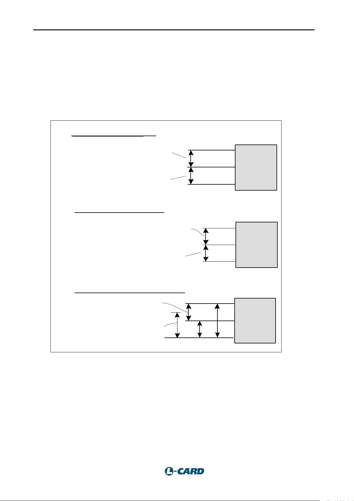
44
Connection of signals.
X
i
Y
i
GND
L-502
Измеряемое напряжение ±10 В или ±5 В
в зависимости от установленного
поддиапазона
Постоянное или переменное напряжение
смещения в диапазоне ±1 В
относительно GND.
Режим “дифференциальный” ±10 В или ±5 В
Режим “с общей землёй”
Измеряемое напряжение
от ±0,2 В до ±10 В в зависимости от
установленного поддиапазона
Измеряемое напряжение ±2, ±1,
±0,5 или ±0,2 В в зависимости от
установленного поддиапазона
Постоянное или переменное
синфазное напряжение (Uxi +Uyi )/2
в диапазоне ±1 В.
Режим “дифференциальный” ±2, ±1, ±0,5 или ±0,2 В
Постоянное или переменное
напряжение смещения GND32 в
диапазоне ±1 В.
U
Yi
U
Yi
U
Xi
-
U
Yi
X (Y )
i
GND32
GND
L-502
U
Xi(Yi)
-
i
U
GND32
U
GND32
X
i
Y
i
GND
L-502
U
Yi
U
Yi
U
Xi
-
U
Xi
Consta nt or alt ernati ng common-mode
volta ge (Uxi + Uyi)/2 in the range ±1
V.
Measured voltage ±2, ±1,
± 0.5 or ± 0 .2 V depe ndi ng on the set
subband
Consta nt or alt ernati ng offset vol tage U y; in
the range of ± 1 V relative to GND.
Measured voltage ±10 V or ±5 V, depending
on the set subband
Constant or alternating offset voltage
GND32 in the range of ± 1 V.
Measured voltage
from ±0.2 V to ±10 V, depending
from the set subband
Mode "with common ground"
Diffe rential mode ±1 0 V or ±5 V
Differential mode ±2, ±1, ±0,5 or ±0,2 V
4.4. ADC input operation voltage range
Note that in the differential mode on the subbands ± 10, ± 5 V, the L-502 has unbalanced
input signal ranges of the inputs X and Y with regard to the analog ground circuit AGND, and in the
"common gro und" mode, the L-502 on the same subbands has asymmetric input signal ranges of the
inputs X (Y) and GND32 with regard to the AGND circuit.
The f i gure below shows e xamples of connecting voltage sources (VS) to the ADC inputs .
Z, Z1, Z2 - the intrinsic resistances of the wires (through which the through currents can flow
with the connection of different devices) or other external electrical causes inducing the parasitic
offset voltag e U
exceed ± 1 V in order to ensure the operating mode, and in the latter scheme the common mode
voltage ( U
Xi +UYi
, UYj.U
Yi
)/2 must be within ± 1 V.
a re i ndica te d. In th e fir st two ci rcu its, the vol ta ge UYi, UYj should not
GND

4.5: Necessary conditio ns for correct connection and co rrect settings of the input of the
X
i
Y
i
GND
L-502
Z1
U
Yi
GND
L
-502
Z
U
Yi
GND32
X (
Y )
i
i
Дифференциальный ИН
и дифференциальный. реж им
L-
502
X
(Y )
j
j
GND
2
GND1
Z2
X
j
Y
j
GND
1
U
Yj
От дал ё нны е одн о ф азн ы е ИН и диф ф. реж им
L-
502
Отдалённая группа однофазных ИН
и ре ж и м с “общей землёй” L-502
Дифф. ИН
X
i
Y
i
GND
L-
502
U
GND
Z
U
Yi
U
Xi
502 program settings, then,
and "with common ground" mode L-502
Remote single-phase VS and diff. L-502 mode
and differential mode L-502
Diff. VS
45
ADC L-502.
Remote single-phase VS group
Differential VS
Exam ples of connecti ng the ADC input are collected in the item
4.5. Necessary conditions for correct connection and
correct settings of the input of the ADC L-502.
Simplified examples of connection of the ADC input are given in section 6.1, however,
4.5.1. The physical causes of possible problems
... If you do not take into account the electrical properties of the signal sources, wires
(cables) when using L-502 ADC connect ions, use the default Lmost likely, you will get a poor result. Why? What do you need to consider? – If you
answer below these questions, links to the Internet resources of the site
!
used.
6.1 on page 59.
en.lcard.ru will be
Physical cause #1. The wide ban dwidt h of the A DC tr ans mis sio n in L -502 (of the order
of 10 MHz) can be not only a great advantage of the L-502 ADC (in the ability of the ADC to
qualitati v el y digiti z e the hig h -speed dynamic processes), but it can be a big problem if:
• the signa l sou rce ha s an un li mit edl y wid e frequ en cy ba nd ( muc h wide r tha n the wi dt h
of the frequencies of the usef ul signal)
• unscreened co nnecti on i s appli ed (or the si gnal sour ce it self ha s a sig nifica nt ar ea of
the unscreened surface), in a si tuation where electromagnetic fields in the frequency

46
Connection of signals.
band up to 10 MH z a r e always pre sent i n the real situ a tio n, an d also i n th e si tu atio n o f
the user' s fai lu re to appl y a differential connec tion (an d adjustme nt to the differe ntial
mode), and therefore use the valuable property of a differential input – effectively
suppressing common-mode interference.
Physical cause #2. The high frequency of the 2 MHz channel switch (when tuned to
multichannel mode) with L-502 default settings may not only be a great advantage of the L-502
ADC (in the high-speed ADC i nput i nter rogat ion) , but i t ca n also be a probl em as it tak es a s hor t
setting time for the measuring circuit (less than 500 ns after the switch's own charge is injected into
the measurement circuit). This cause is fundamental for all ADC with input commutator,
manifes ted as a switching disturbance.
4.5.2. Conditions for correct connection and settings L-502.
1. If you need to use no more than 16 ADC channels, always select the differential
connection m ode and the L-502 set tings.
2. With a differential connection, the X and Y circuits of each channel always lead in pairs
(twis ted pair, shielded pair ).
3. The L-502 si gnal circuit must be shielded. On the screen connection, see
4. For differ e n tial co nnec t i o n , w he n u sing a pa i r ca ble, to maxi mize c o mmon -mode
rejection of the L-502, the output impedances from the remote sourc e a long the X and Y
circu i ts shou ld be balanced, (connect io n e xa mple - p.
6.1.10).
5. The AGND L-502 circuit must be connected to the common circuit of the si gna l sour c e
(if there are several signal sources to the common junction of the common signal source
wires).
6. If you ne e d to c onfigu re the L -502 for mult ichannel operation, you first need to optimize
the si gnal-to-noise ratio of the ADC in a single-channel operation mode with a
maximum dat a a c qu i s it i on frequency of 2 MHz, i n which in t h e si g na l s pe ct r u m you w i ll
see all the frequencies of the interference (possibly from "mirror frequencies", if
interfer e nc e a b ove 1 MHz) , wh i c h m eans tha t you have a t oo l i n y ou r ha n ds t o fi n d t h e
sourc es and caus e s of these interfere nce s (before going to multi-channel mode and
averaging mode, which wi ll b e much mor e diffi cu l t t o u nd ersta n d with sources of
interference).
4.2.2.
7. When usi ng ("de fault") in t he m ult i-channel operation mode of the maximum
switching frequency (2 MHz), the output impedance of the L-502 signal cir cuit must
be from 0 to 50 Ω (in the frequency band up to 10 MHz), and this voltage source
must be li nk ed t o con nector L-502 by w ires of zero lengt h. This is achieved either by
directly connecting the output of the signal source itself (50 Ω) or by connecting its load
resistor (up to 50 Ω) directly to the cable part of the L-502 signal connect or (when
connecting a n agreed 50-ohm line or a current shunt to 50 ohms of the external curren t
measurement circuit) .
8. When using a multichannel mode of non-zero length of wires t o the voltage source
and (or) with an outpu t resistance of the s ignal cir c uit of more than 50 ohms, t he
program set ting of the s ignal con ditioni ng time n
> 1 (s. 3.3.6) should be applied.
su

47
4.5: Necessary conditio ns for correct connection and co rrect settings of the input of the
ADC L-502.
9. In mult i-channel mode, the optimal settling time nsu (s. 3.3.6) should be selected
depending on the output impedance of the signal source, the length and the
coherence of t he cable. It is sugges te d to choos e the opt imal n
for this channel by the
su
crit er i o n of obtaining a s ma ll inter-channel signal transmission from the previous polling
channel.
10. To improve the signal-to-noise rat io and increase t he resolution in the
measurement path, it is recommended to use the maximum possible avera gi ng
factor n
signal conditioning t ime n
11. Do not exceed the operating vol tage ranges at the inputs X , Y, GND32 (s.
> 1 (s. 3.3.6) for the required channel polling frequency and the necessary
av
.
su
4.4)
12. Use the L-502 "common ground" opera tion mode only in case of closely located low-
resistance sources. Optimizing the n
and nav sett ings for the "commo n gr ound" mod e is
su
required. Do not make "common ground" connections through the cable, if there are no
low-resistance pull-up r e s i stors on th e L -502 side .
13. Whil e co n ne cting L-502 "with common ground", the GND32 circuit must be in the same
grou p of cable wires (in particula r, wi thin the same scr ee n) a s other cir cuit s X and Y
opera ting in t h e " c om m on grou nd" sch eme.
14. While us ing 16 to 31 c hannels , it is advisable to combine L-502 "dif feren tial" and
"common ground" connections and settings to obtain more channels operating in
differential mode. In this case, the wires X and Y (differential circuit) and the wires X,
Y, GND32 ("common ground" circuits) should form different groups in the cable in a
common AGND circuit situation for these groups.
15. When using L-502 w itho ut galvanic isolation, do not allow continuous currents on the
screens and common wires of the signal circuits. Do no t allow continuous cu r r e nt s
between common-wire circuits of digital and analog signal circ uits. Take into account
the internal scheme of land connection in L-502 (s.
4.1)

48
Connection of signals.
4.6. Calculation of the total load power of L-502 output
circuits
If you intend to us e L-502 output circuits to connect any external loa ds, then t he tota l load
power should not exceed the power specified in the specification (see section
load power sho uld be es timated accord ing to the pr ocedure describe d below .
5.7 on p. 56). The
The total load power
where
loads connected t o the GND circuit );
In turn, the power summ ands
through the known load current
resistance
The power summ ands
is t he total load pow er taken from digital D O outputs i n the "1" state (only for
— power load removed f r om the DAC outputs;
— power load, take n from the output of +15 V;
— power load, take n from the output of -15 V;
— power load, take n from the output of +3.3 V;
at the i-th output
taken f r om the L-502 power system is:
by the f or m ula , or through the know n load
of the c or r e s ponding j-th outputs must be c alculate d eit he r
of the c or r e s ponding i -th outputs m us t be calculate d either
through the known load current
resistance
The power
resistance
All terms in the power formulas ar e pos itive , dimens ion: power — Watt, current — Ampere,
resistance — Ohm
at the j-th output
and should also be c alculate d either through known load currents
by formulas , or through a know n load
, accordi ng to formulas ,
by the f or m ula , or thr ough the known load

49
!
Parameter
Value
Number of cha nnels
16 differential or
DC Voltage Measurement Range
±10 V
Analog-to-digital conver ter b it d e p th
16 bits
ADC data width after arithmetic processing (data correction, data
24 bits
Li mits of the permis sibl e redu ce d basi c er ror o f DC volta ge
– 10; 5 and 2 V
±0.05
– 1 V
±0.07
– 0.5 V
±0.1
– 0.2 V
±0.2
Possibi lity of data correction (use of calibration coe f ficients)
Yes
Chapter 5. Specifications.
The following specifications indicate the main parameters of the L-502 for its intended -
opera ting m od e .
For the max imum permissible volt age s and currents at t he contacts of the connectors,
4.3
see section
5.1. ADC.
, on p. 42
Volt age measurement subra nges
(the input signal is applied between Xi and Yi for 16 -channel
mode, between Xi (Yi) and GND32 for 32-channel mode)
Operating conditions of measurement at the ADC inputs (s. 4.4,
p. 44):
- Voltages at the input Yi with regard to AGND f or the
differential measurement mode on the subba nds "± 10 V", "± 5
V"
- The a verage value of the voltage at the inputs X and Y for the
differential mode on the measurement subranges "± 2 V", "± 1
V", "± 0.5 V", "± 0 .2 V"
- Voltages at the GND32 input relative to AGND for the
"common ground" mode and all measurement subbands
averaging)
measurements, %, in subbands:
32 wit h common ground (singl e-phase)
±10 V, ±5 V, ±2 V, ±1 V, ±0.5 V, ±0.2
V when obse rving the ope rating
conditions of the measurement (see
below)
| ≤ ±1 V
|U
X
+ UY)/2 | ≤ ±1 V
| (U
X
GND32
| ≤ ±1 V
|U
Own input cur rent (via X, Y or GND32 circuits) in single-channel
mode, no more than
Charge injection into the input circuit of the ADC (X, Y or
GND32) for one switc hing
0.4 µA
2 pC

50
Common-mode rejection ratio 50 Hz with 1 V amplitude in
±10 V
77 dB
±5 V
83 dB
±2 V
90 dB
±1 V
92 dB
±0.5 V
92 dB
Limits of the permissible relative fundamental error of the ADC
±0.005 %
AC voltage measurement range
From 0.2 mV to 7 V
)]1(02,015,0[ −×+±
X
X
AC
)]1(02,03,0[ −×+±
X
X
AC
more than 100 to 300
)]1(03,01[ −×+±
X
X
AC
)]
1(
05,0
5[
−×+±
X
X
AC
Notes:
the ADC conversion frequency of 2000 kHz, for signals whose peak values do not exceed the value of
2
К
AC
X
X =
4 X is the value of the measured voltage.
di ff erential mode on sub-band:
±0.2 V 92 dB
Resistance to overloa ds by input mea suring signal of DC voltage ±15 V
conversi on f requency
Limits of the permissible relative basic error of measuring the AC
voltage
According to section
5.1.1. Limits of the permissible relative basic error of measuring the AC voltage
Frequency range of
input signal,
kHz
from 0.01 to 50 incl.
more than 50 to 100 incl.
incl.
more than 300 to 999
1 The error in measuring the AC voltage is normalized in the differential connection scheme E-502 at
Limits of the permissible relative basic
error of mea s uring the AC voltage, %
the set m easure m e nt subba nd .
2 XAC is the AC voltage mea surement limit,
where XK is the value of the set voltage
subband.
is the final value of the set voltage subband.
3 X
К

51
Data entry rate,
Averaging
ADC subrange, V
±10
±5
±2
±1
±0.5
±0.2
Typical value of the noise level, applied to the
2000
1
309
157
50
37
22
18
50
20
62
27
13 8 6 4 10
128
40
25
12 7 5
4
Signal source resistance
Channel polling time, μs (with averaging factor equal to 1) o r
Interch annel traversal, dB
0-50 Ohm
-65
-78
-82
-82
-82
-82
5.1.2. ADC own input noise.
Below are the typi cal noise levels without taking into account the factors of temperature and
long-term zero drift for 1-channel mode with a shorted ADC input.
Kword/s
from one ADC
channel
400 5 127 56 28 16 12 8
factor
5.1.3. ADC inter-channel passing.
(in t he channel where the interchannel
passage is measured)
ADC input, μV
channel setup time, μs
0.5 1.0 2.0 4.0 8.0 16.0
(the si gnal from the pr evious channel in the order of
interrogation)
1 kOh m -35 -63 -73 -82 -82 -82
10 kOhm -5 -11 -22 -43 -74 -82

52
Parameter
Value
Number of cha nnels
2
DAC bit depth, bit
16
Output mod es
Synchronous (strea mi ng) , asynchronous
Output si gnal range
±5 V
Limits of the allowed reduced basi c error of reproducing DC
±0,3 %
Maximum al lowable output curre nt1
±20 mA
From 1 mV to 3.5 V
AC voltage playback error
According to section 5.2.1
Output voltage
Limits of th e permissibl e rela tive basic error of A C
)]1(02,015,0[ −×+±
X
X
AC
)]1(02,05,0[ −×+±
X
X
AC
Notes:
5.2. DAC.
Output fr equency i n sync hr onous mode 1 Mcount/s per channel
Output fr equency i n asynchr onous mode The actual speed depends on many
factors of the software and hardware
environment.
Operating range of output currents ±10 mA
voltage
AC voltage playback range
5.2.1. AC voltage playback error
frequency, KHz
From 0.01 to 50 inclusive
From 50 to 100 inclusive
1 XАС – the fin a l value of the range of A C voltage playback, X
2 X is the value of the voltage to be reproduced.
playback vol tage, %
= 3.5 V.
АС
1
If the total load power is not exceeded, see s. 4.6 Calculation of the total l oad power of L-502 output circuits

53
Parameter, charact eristics
Value, description
Data entry modes
Synchronous, asynchronous
Program control of pull-up resist or s a ctivation:
- for input s DI1-DI16
Regardless of the hi gh and
- for input s DI_SYN1, DI_SYN2
Regardless of each input
Maximum speed in synchronous mode
2 Mw o r ds/s
Maximum speed in asynchronous mode.
The actual speed depends on
Recommended operating volta ge range
0 …+5.5 V
Operating voltage range
-0.2...+0.6 V ("logical zero")
Own input cur rent in operating mode with software-activated pull-up
10 µA
Pull-up resistor r esistance
2.2 kOhm wit h r egard to
Recommended edge duration:
5.3. Digital inputs.
Total numbe r of digital inputs (DI1-DI16, DI_SYN1, DI_SYN2)
Of the se, the number of digital inputs with synchr onizati on f unction
(DI_SYN1, DI_SYN2)
Maximum permissible input voltage range:
- at the inputs DI1-DI16
- at the inputs DI_SYN1 , DI_SYN2
High-impedance state with power off Yes
Maximum input current with power off 10 µA
18
2
low byte
many factors of the software
and hardware environment.
–0.5…+6.5 V
–10…+10 V
+2.4...+5.0 V ("logical
item").
resistors
+3.3 V
- at the i nput DI1-DI16
- DI_SYN1, DI_SYN2
The input hysteresis voltage DI_S Y N1, DI_SYN2, typical value 400 mV
0…50 ns
Not limited
54
Parameter
Value
Number of digital outputs of gene ral purpose
16
Maximum speed in synchronous mode
1 KWords/s
Maximum speed in asynchronous mode
the act ual speed depe nds on many
Maximum permissible current2 in the load circuit
20 mA
Voltage range at digital outputs
0...+0.4 V ("logical ze r o")
Output resistanc e, typical val ue
110 Ohm
Maximum leakage cu rr en t in op erating mode in high-impedance
±1 µA
Parameter
Value
The reference frequency of the process of synchronizati on of data
1.5/ 2.0 MHz
5.4. Digital outputs.
Contr ol of the third state of outputs Byte
Data entry modes Synchronous, asynchronous
factors of the software and hardware
environment.
Recommended curr en t in the load circuit max . 8 mA
state
High-impedance state with power off No
5.5. Synchronization in L-502.
5.5.1. Synchronization characteristics
collection and output of ADC, DAC, digital input and output:
• For a si ngle module
• For a mul tiple module synchronization
max. 2 .4 V ("logical unit").
Output logic elements with a supply
voltage of 3.3 V
1.5/ 2.0 MHz
1,5 MH z
Limits of the permissible relative fundamental error of the
reference frequency
2
If the total load power is not exceeded, see s. 4.6 Calculation of the total l oad power of L-502 output circuits
±0.005

55
Parameter
Value
Topology of m ultimod ule connections over synchronizati on lines
Sequence
Maximum number of synchronized L-502 modules in a serial
Equal to the number of PCI-E slots in
Maximum cable length of the intermodule synchronization
40 mm (only for a n adjacent module
Number of intermodule synchronization lines
4 twisted pairs (2 inputs from the master
Sta ndard for an interface with a computer
PCIe x1
The bit depth of the L-502 dat a word on the PCIe
32 bits
DMA support in the BUS MAS TER mod e on the PCle
Yes
Interface wi th a computer
HOST DMA 16 bits
Main control inte r face
SPI
SDRAM interface
32 MB; 16 bit; 132.5 MHz
Debugging interface
JTAG
Compatibility with JTAG emulators Analog De vices
ADZS-ICE-100B,
5.5.2. Intermodule synchronization interfac e
synchronization scheme
the PC motherboard
PCI-E)
and 2 outputs to the sl ave)
5.6. Characteristics of standard interfaces.
Parameter, charact eristics Value, description
Interface with a computer
Interfaces of the signal processor ADSP-B F523 (L-502-P)
Main interface of input-output for ADC, DAC, digit al I/O SPORT0, >120 Mbit/s, duplex
ADZS-USB-ICE,
ADZS-HPUSB-ICE.

56
Parameter, charact eristics
Value, description
The c ondition of galvanic isola tion in a
If in all connected L-502 there is galvanic isolat ion
Galvanic isolation border
Between all circ u its tha t co me to th e co ntac ts of signal
Galvanic isolation border in a system of
Between all circuits that come to the contacts of all signal
The maximum permissible voltage rise rate
Total load power take n f r om all outputs
For L-502-░-░-D (wi th DAC)
0.4 W
External analog power su pply outputs
+15 V, -15V. The maximum load curr ent is up to 30 mA,
External digital circuits supply output
+3.3 V . T he operating cur r ent of the load is up to 50 mA
Maximum current consumed from PCI
“+3.3 VAUX”
0.02 А
5.7. Power supply system and galvanic isolation.
L-502 modi f ications, whic h have gal vanic
isolation
system of several L-502 connected vi a a
synchronization interface
several L-502 connected via a
synchronization interface
Test voltage of gal vanic isolat ion 500 V during 1 min.
L-502-P-G, L -502-P-G-D, L-502-X-G, L-502-X-G-D
connectors, and PC circuits.
The metal case DR B-37M is not galvanically isolated from
the PC.
connectors L-502, and PC circuits.
The metal housings DRB-37M are not galvanically isol ated
from the PC. Between themselves all the signal circuits in
the syste m will not be galvanically isolated
10 kV / μs
between galvanically isolated circuits in L502-░-G-░
The method for estima ting the load power is given in p. 4.6,
L-502:
p. 48
For L-502-░-░ (without DAC) 0.8 W
Expres s uni t through circuits:
“+12 V”
“+3.3 V”
provid ed that the total load power is not exceeded. SC is
prohibited. Outputs are switched on by jumpers, (see p.
2.1.2), this possibility is dependent on whether the
corresponding outputs of the DAC are used
permanently, up to 100 mA for a short time.
Attention! In versions 1 and 2 of L-502 pr oducts (seria l
numbers start with the digit "1" or "2", short circuit of the
output + 3.3 V is not allowed (leads to failure of L-502)!
In version 3, short circuit of the output is permissible.
0.4 A
0.35 А for L-502-X-░-░
0.85 А for L-502-P-░-░

57
Maximu m power consumed from PCI
Expres s uni t
Maximum permissible through-current by
the circuits of one L -502 module:
3
AGND-DGND
GND-DGND (L-502 without galvanic
isolation)
GND-AGND (L-502 without galvanic
isolation)
Maximum permissible through curre nts
along AGN D-AGND, AGND-DGND,
DGND-DGND circuit s of d ifferent L-502
module s c onnected by a synchronization
cable
6 W (for L-502-X-░-░)
7.6 W (for L-502-P-░-░)
100 mA
100 mA
100 mA
50 mA
3
The notion of circuits GND, AGND, DGND is introduced in section 4.1

58
Parameter
Value
Parameter
Value
– environment temperature, °С
– relativ e humid it y, %
– air-pressure, kP a
For stability under climatic influence s, the converte r s, in addition to the
– environment temperature, °С
– air-pressu re, kPa
– environment temperature, °С
– air-pressure, kP a
5.8. Construction specification.
Construct PCI Expres s C ARD x1 of standa rd height, with bracket, in length - less than
half the size (HALF LEN GTH), according to PCI E xpress Card
Electromechanical Specification rev.2.0.
Requires one PCI Express crate slot.
Overall dimensions of the
print ed circuit board
- length x height
136 x 101 mm
5.9. Environmental conditions.
5.9.1. Normal conditions
Nor ma l operat i n g c on diti on s:
from 30 to 80
from 84 to 106
5.9.2. Operating conditions
20±5
Parameter Value
versions with the le tter index I, c or respond to GOST 22261, group 3 with
an exte nded range of operating te mper atures:
– relative humidit y at an ambient temper ature of 25 °C, %
For stability under climatic influence s, converters of designs with the letter
ind ex I correspond t o GO S T 22261, group 4 with an extended range of
operating temperatures:
– relative humidity at an ambient temperature of 30°С, %
from +5 to +55
up to 90
from 70 to 106.7
from -40 to +60
up to 90
from 60 to 106.7

59
!
tion examples should be considered together with the recommendations for
L-502
X1 (X2-X16, Y1-
Y16)
AGND
GND32
Uвх
L-502
AGND
X1 (X2 -X16)
Y1 (Y2 -Y16)
Uвх
L-502
AGND
X1 (
X2-X
16, Y
1-Y16
)
L-502
GND32
X1 (X2-X16, Y1-Y16)
L-
502
X
1 (
X2 -
X16
)
Y1
(Y
2 -
Y16
)
Chapter 6. Connexion samples.
These connec
connecting and configuring the L-502 (n.4.5).
The short form of information provided in this chapter does not cover all the features of the
connection for your particular case. If necessary, please contact: en@lcard.ru
site en.lcard.ru
.
6.1. ADC entry point co nnection
or in the conference on the
6.1.1. Connecting to the ADC entry point of single-phase voltage source
6.1.1.1. Up to 32 channels. Mode "with
common ground"
Forbidden to connect in this way!:
6.1.1.2. Up to 16 channels. "Differential"
mode

L-502
X1 (X2 -X16)
AGND
L-502
Y1 (Y2 -Y16)
AGND
R1
R2
L-502
AGND
GND32
X1 (X2-X16, Y1-Y16)
X1 (X2 -X16)
Y1 (Y2 -Y16)
R1
R2
L-502
AGND
The voltage transfer ratio is R2/(R1+R2).
R1
R2
L-502
AGND
GND32
X
1 (X2
-X16
, Y1-Y16)
С
R1
R2
L
-502
AGND
С
X1
(X2 -
X16)
Y1 (Y2 -Y16)
It is necessary that R2 should not be more than 50 ohms if the switching frequency is maximal.
С
R2
L-502
AGND
GND32
X1 (X2-X16, Y1
-Y16)
С
R2
L-502
AGND
X1
(X2 -X16)
Y1 (Y2 -Y16)
60
6.1.1.3. Voltage divisor.
Mode "with co mm on grou nd"
It is necessary that R1 or R2 should not be more than 50 ohms if the switching fr equency is
R2 should be located clo se to the L-502 entry point.
6.1.1.5. Integrating cir cuit .
Mode "w ith co mm on grou nd"
6.1.1.4. Voltage divisor.
"Differ enti al" mo de
maximal.
6.1.1.6. Integrating cir cuit .
"Differ enti al" mo de
The transmission coefficient of the voltage in the frequency band is R2/(R1+R2).
If multichannel mode , i t is necessary that 1/F
present, then 1/F
>> R1*(C+10
ADC
-10
)/R1, where F
>> R1*R2*(C+10
ADC
is the ADC conversi on frequency.
ADC
-10
)/(R1+R2), or if R2 is not
R2, C sh ould be located cl ose to the L-502 entry point.
6.1.1.7. Closed entry. Mode "with common
earth"
6.1.1.8. Closed entry. Mode
"differential"
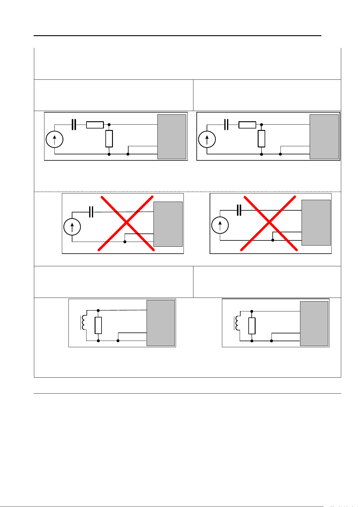
The connection is recommended for sin gl e-channel mo de.
R2
С
R1
L-502
AGND
GND32
X1 (X2-X16, Y1-Y16)
R2
С
R
1
L-502
X
1 (
X
2-
X16
,
Y1
-Y
16
)
Y
1 (
Y2
-
Y16)
AGND
С
L-502
AGND
GND32
X1 (X2-X16, Y1-Y16)
С
L-502
AGND
X1 (X2 -X16)
Y1 (Y2 -Y16)
Can not be connected like this!
R
L-502
AGND
L
X1 (X2-X16, Y1-Y16)
GND32
R
L-502
AGND
X1 (X2 -X16)
Y1 (Y2 -Y16)
L
61
R should be located close to the L-502 entry.
6.1.1.9. Closed entry with divider. Mode
"with common ground"
In mult i-channel mode, the connect ion is correct only f or R2 < < R 1 and R2 ≤ 50 Ω.
R2 should be located clo se to the L-502 entry point.
The tr ansmission coef ficient of the voltage in the passband is R 2/(R1+R 2).
6.1.1.10. Closed entry with divider.
"Differe nti al" mod e
6.1.1.11. Inductive pickup.
Mode "with common ground"
6.1.1.12. Inductive pickup.
"Differe nti al" mode
Resistor R performs the function of a damper to suppress the oscillation process in the L-C circuit ,
where C is the equivalent total capacitance applied in par allel to L. The ADC en try capacitance is
estimated to be 25 pF. Resistor R should be locate d clos e to L-502 input.

62
L-502
AGND
Uвх
Y1 (Y2 -Y16)
X1 (X2-X16)
R
1
L
-502
AGND
X1
(X2
-X16
)
Y1 (
Y2 -
Y16)
R
2
(R1 = R2) ≤ 50 Ω, if the switching frequency
R
1
L-502
AGND
X1
(X2
-X16)
Y1 (Y2 -Y16)
R2
R3
R4
R1
L-502
AGND
X1 (X2 -X16)
Y1 (Y2 -Y16)
R2
L
R1
L-502
AGND
X1 (
X2 -X16)
Y1 (Y2 -Y16)
R2
R3
R4
6.1.2. Connection to ADC input with up to 16 differential voltage sources
6.1.2.1. General ca s e
Only for voltage s ubranges of L-502: ± 2 V , ± 1 V, ± 0.5 V, ± 0.2 V.
6.1.2.2. Differential co nne cti on of an
isolated volt ag e so urce
The following condition should be met :
is maximal.
Allocate R1, R2 close to
L-502 entry.
Only for voltage s ubbands:
± 2 V, ± 1 V, ± 0.5 V , ± 0.2 V.
6.1.2.3. Different i al co nne cti on of an
isolated voltage source with divider
It is necessary: R1 ≤ 50 Ω, if the switching
freq ue ncy is max imal, R1 = R 2, R3 = R4..
Allocate R1, R2 close to L-502 input. The
voltage transfer ratio is
(R1+R2)/(R1+R2+R3+R4)
Only for voltage s ubbands:
±2 V, ±1 V, ±0.5 V, ±0.2 V
6.1.2.4. Special case: diff ere nti al connection of the inductive sensor:
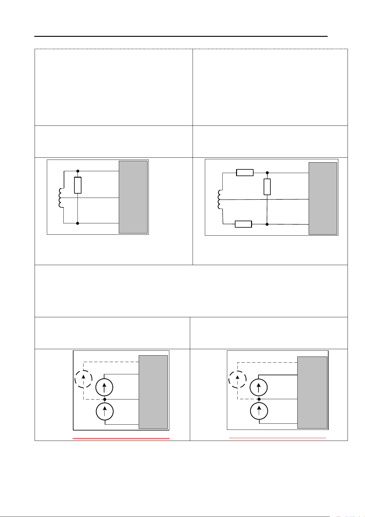
Only for voltage s ubbands:
Only for voltage s ubbands:
R1
L-502
AGND
X1 (X2 -X16)
Y1 (Y2 -Y16)
L
R1
L-502
AGND
X1 (X2 -X16)
Y1 (Y2 -Y16)
R2
R3
L
L-502
X2 (X3-X16, Y1-Y16)
AGND
GND32
Uвх1
Uсм
X1
Uвх2 (3-16)
L-502
AGND
Uвх1
Uсм
Uвх2 (3-16)
Y1 (Y2 -Y16)
X1
X2 (X3 -X16)
63
±2 V, ±1 V, ±0.5 V, ±0.2 V
6.1.2.5. Differential winding connection
with midpoin t
Locate R1 close to L-502 entry point
Only for voltage subranges of L-502: ±2 V,
±1 V, ±0.5 V, ±0.2 V
±2 V, ±1 V, ±0.5 V, ±0.2 V
6.1.2.6. Differential winding connection
with midpoint through the div id er
Locate R1 close to L-502 input.
Only for voltage s ubranges of L-502: ±2 V,
±1 V, ±0.5 V, ±0.2 V
6.1.3. Connection to the ADC input for the case where the common wire of the
signal sources has a offset potential Ucm of max. ± 1 V r e lat ive t o t he A G ND
circuit.
6.1.3.1. Connection up to 32 channels.
Mode "with co mm on grou nd"
See limitations in section 4.4, p. 44!
6.1.3.2. Connection up to 16 channels.
"Differe nti al" mod e
See limitations in section 4.4, p. 44!

64
R2
L
-502
AGND
X1 (X2 -X16)
Y1 (Y2 -Y16)
R
3
R1
This connection allows you to measure the voltage
, the equivalent impedance referred to
It is necessary that R2
R1
L-502
AGND
X1 (X2 -X16)
Y1 (Y2 -Y16)
L
Uсм
GND
L-502
GND32
X (Y )
i
i
GND1
GND3
Y
k
X
k
X (Y )
j
j
Y
r
X
r
GND2
Дифф.
ИН
Diff. VS
6.1.4. Measurement of the voltage drop on the circuit section in the differential
mode (up to 16- channels)
drop across resistor R2. Fo r a single-channel mode , R1,
R2, R 3 ca n a l s o b e i mpeda nces of a capac i tive or indu ctive
nature, but with the condition that the circuits X and Y
used a re not brok en by th e dire ct curr ent o f the cir cuit . In
mult ichan nel mo de
the ADC input must be active.
should not be more than 50 ohms if the switching
frequency is maximal.
See limitations in section 4.4, p. 44!
6.1.5. Differential connection of the transformer (throttle) winding with midpoint and
offset potential with respect to AGND
Limitations:
|Ucm| ≤ 1 V
Only for the voltage subbands L-502:
±2 V, ±1 V, ±0.5 V, ±0.2 V
6.1.6. Example of mixed connection of voltage sources "with common ground" and
differential.

65
R
I
L-502
AGND
GND32
X1 (X2-X16, Y1-Y16)
Y1 (X2-X16)
R
I
L-502
AGND
X1 (Y2 -Y
16)
Fixed ADC ± U subband must correspond to U=I
*R, and the current source must have a voltage
Y1 (X2-X16)
R
I
L-502
AGND
X1 (Y2 -Y16)
Uсм
R1
L-502
AGND
X1 (X2 -X16)
Y1 (Y2 -Y16)
R2
I
R = R1 + R2
Fixed ADC ± U measurement subband must correspond to U=I
*R, while the current source
6.1.7. Connecting a power supply to the ADC input
6.1.7.1. Mode "with common ground" 6.1.7.2. Differential mode
MAX
margin of at least U. Resistor R should always be located close to the ADC in pu t. In any case, the r e sistor
R must be less than 50 Ω in the multi-c hanne l m ode at t h e maximum switchin g frequ ency.
6.1.7.3. Differential mode, offset potential
due to current source in regard to AGND
6.1.7.4. Differential mode, isolated
current sour ce
Only fo r the voltage subbands L-502: ±2 V, ±1
V, ±0.5 V, ±0.2 V
MAX
must ha ve a v olta ge mar gin o f, at lea st, U. R esi stor R s hould a lwa ys be lo cat ed clo se to the ADC i nput.
Resistors R, R1, R2 must be less than 50 Ω in multichannel mode at the maximum switching frequency.
|Ucm| ≤ 1 В

66
R
=
Zв
L-502
AGND
GND32
X
1 (
X
2
-
X
16
, Y1-
Y16)
Zв
Y1 (Y2-Y16)
L-502
AGND
X1 (Y2 -Y16)
Zв
R=Zв
R1
L-502
AGND
X
1 (X
2 -X
16)
Y1 (Y2 -Y16
)
R2
Zв
6.1.8. Consistent connection of remote current sources or voltage through a long line
with a wave resistance of Zw with load on the side of the receiver.
(If the signal source has an output impedance, unequal to Zw, then these cases correspond to one-way
matching of the long line on the side of the signal receiver )
6.1.8.1. Mode "with common ground" 6.1.8.2. Diff er enti al mo de
6.1.9. Differential connection of an isolated current source or voltage
R1=R2
R1+R2 = Zw
The ci rcui t is val id onl y for t he foll owi ng volt age
subranges L-502:
±2 V, ±1 V, ±0.5 V, ±0.2 V

67
Y1
(Y
2
-Y
16)
L
-502
AGND
X
1
(Y
2
-Y
16)
R
=Z
в
R
ВН
=
Zв
/2
R
=
Zв
/2
Источник
напряжения
Y1 (Y2-Y16)
L-502
AGND
X1 (Y2 -Y16)
R=Zв
R1=Zв/2
R
2
=Zв/2
Источник
напряжения
Вход
Voltage
Voltage
Input
6.1.10. The coordinated connection of a remote voltage source through a pair of
long line with a wave resistance Zw with matching on the signal source side
source
– internal (output) impedance of the signal source.
R
BH
R – balancing resistor on the signal source side.
The cable must be paired (shielded twisted pairs) with wave resistance of wire pairs Zw.
Bel ow i s a pra cti cal ca se wh ere a broa dba nd o pera ti onal ampl ifi er a cts a s a remo te v olta ge sour ce
(providing a low-impedance voltage output in the frequency band up to 10 M Hz).
source

68
L-502
-░-░-D
DAC1
DAC2
AGND
Rн1
±5В
±5В
DAC1
DAC2
AGND
Rн
±10В
±5В
±5В
L-502
-░-░-D
The differential output ±10 V is realized as a
6.2. Connecting the DAC outputs.
To realize the DAC function in L-502-░-░-D, the outputs DAC1 and DAC2 must be
precon figur e d w i th ju mp er, s ee s ec t ion
6.2.1. 2-channel outp ut ± 5 V 6.2.2. Single-channel differential output ±10
2.1.2 o n p. 15
V
difference voltage between the outputs DAC1 and
DAC2

69
DO (1-16)
GND
R
L-502
The LED is lit when the DO output is at the
R
+3.3V
L-502
DO (1-16)
+3.3V
R1
DI (1-16)
AGND
K1
L-502
DI_SYN1,2
+3.3V
R1
DI (1-16
)
AGND
K1
L-502
DI_SYN1,2
6.3. Connecting the digital inputs and outputs.
6.3.1. Connecting the LED or the optron input. Option 1
"log ical unit".
6.3.2. Connecting the LED or the optron input. Option 2
The LED is lit when the DO output is at the
"log ical zero".
6.3.3. Connecting a contact to a digital input
6.3.3.1. Option 1 6.3.3.2. Option 2
A logi ca l unit correspond s
to an open contact. The
recommended resistor R1
nominal is from 3 to 5
kOhm.
R1 is n ot re quir ed if t he
internal pull-u p resist or i s
programmed on the
corresponding input.
The ope n contact
corresponds to a logical
zero. The recommended
resistor R1 nominal is
from 3 to 5 kOhm. In
this cas e, th e intern al
pull-up resistor should
be turned off.

70
DI_SYN1
GND
DI_SYN2
L-
502
6.3.3.3. Connect the optron output to the synchronization input
The digital inputs DI_SYN1,2, which can be used
as synchronizat ion inputs, are adapted to directly
connect the optr on output. The internal pull -up
resistor of the DI_SYN1,2 input must be softwareenabled.

71
Chapter 7. Dimensional drawing
The dimensions are in millimeters.

72
Bibliography.
[1] L-502. Progra mmer guide. - M.: L-Card, 2013
[2] Low-level programmer manual for the L-502 board. - M .: L-Card, 2013
[3] A. V. Garmanov. - "Connection of mea suring devices. Electr ical compat ibility and noise i mmunity".
- M.: L-Card, 2003
[4] T erminology for measuring systems – technical support section on the L-Card website:
www.lcard.ru/lexicon
[5] Error! Hyperlink reference not valid.
List of tables.
Table 4-1: Eterna l signa l connector ....................................................................................................... 34
Table 4-2: I nt ernal si gnal c on n ec t o r ...................................................................................................... 37
Table 4-3: Intermodule synchronization connector .............................................................................. 39
Table 4-4 The maximum permissible modes are described for the L-502 module installed in the
computer's system unit ................................................................................................................... 42
Table 4-5Maximum permissible thro ugh current by GND, AGND, DGND ...................................... 42
List of figures
Fig. 1-1. Symbol system for L-502 module ............................................................................................ 7
Fig.1-2. L-502 versi on 3 (face layout) .................................................................................................. 11
Fig. 1-3. L-502 versio n 1 or 2 (face layout ) ......................................................................................... 12
Fig.1-4. L-502 ( bac k layout) ................................................................................................................. 13
Fig. 3-1. Illustration of the personnel princip le for acqui ring ADC data ............................................ 23
Fig. 3-2. L-502 synchronization system structure................................................................................. 25
Fig. 3-3. The principle of obtaining ADC data (in detail) ................................................................... 27
Fig.3-4. Synchronous I/O diagram........................................................................................................ 29
Fig. 3-5. Block diagr am .......................................................................................................................... 31
Fig. 4-1: Eternal signal connector .......................................................................................................... 34
Fig. 4-2: Internal si g na l c on n ec t or ......................................................................................................... 36
Fig. 4-3: Example of a grouped connection of digital lines: three buses of 8 bits each. .................... 38
Fig. 4-4: Intermodule synchronization connector (L-502 version 1 and 2). ....................................... 38
Fig. 4-5: Intermodule synchronization connector (L-502 version 3)................................................... 39
Fig. 4-6: Multi-module synchronization scheme .................................................................................. 40

73
Fig. 4 -7: The scheme o f mult i-module synchronization of three L-502 ver sion 3 (top view of the
computer ' s m otherb oa r d ) ................................................................................................................ 40
Fig. 4-8: Intermodule synchronization cable L-502-SYNC ................................................................. 41
Fig. 4-9. JTAG ........................................................................................................................................ 41
 Loading...