


A family of universal modules of the ADC, DAC
Measuring voltage converters
E-502-P-EU-D-I
E-502-P-EU-D
E-502-X-EU-X
E-502-X-U-D
E-502-X-U-X
User manual
Revision 1.1.0
October 2017
http://en.lcard.ru
en@lcard.ru
DAQ SYSTEMS DESIGN, MANUFACTURING & DISTRIBUTION

L-Card LLC
117105, Mosc ow , Varsha vskoye shosse, 5, block 4, bld. 2
tel.: +7 (495) 785-95-19
fax: +7 (495) 785-95-14
Internet contacts:
http://en.lcard.ru/
E-Mail:
Sales department: en@lcard.ru
Customer care: en@lcard.ru
E-502 Module © Copy right 2014-2017, L-Card LLC. All rights reserved.
Revis ion hist or y of this document
Date
Document
Contents of the change
09.2014
1.0.0
Prelimin ar y data
05.2015
1.0.1
The ope r ating tempera ture range has been changed (
),
05.2016
1.0.2
10.2016
1.0.3
01.2017
1.0.4
1-1
5.3,6.3
01.2017
1.0.6
1.1.1
2.1
02.2017
1.0.7
Pa ragraph added 3.3.4.1
06.2017
1.0.8
Comments are added to sec. 2.3.3, section is added. 2.8
06.2017
1.0.9
3.3.5.2
10.2017
1.1.0
Added indu strial design versions.
3.3.8
4.7
revision
fig. 1-1
upgraded Chapter 2, Chapter 4. Added section 4.8, Chapter 7,
technical data corrected – Chapter 5.
Orde r option E-502-X-EU-X has been added to the sec tion 1.1.
Fixe d bugs i n the drawings 6.3
Information on the industrial design versi on is included. Amended fig.
.
01.2017 1.0.5 The e r r or about the presence of pull -up resistors on DI inputs is
corrected (s.
The ope r ating tempera ture range in the table of section 5.9 has been
brought into correspondence, amended the section 5.8, the tables in
subparagraphs
)
are amended,
A warning i s added to item.
The characteristics according to the results
of prepar ation of the family of L-CARD voltage measuring converters
for cer tificati on as Means of Measure ment are brought into
correspondence.
Added to item
. Paragraph added
W he n r eading this document elec tronical ly, t o faci litate navigat ion, use the electroni c tree
of the t able of content s (for exampl e, Acrobat Reader) , as well as hyperl inks wit hin the document.

Contents
CHAPTER 1. GE NER AL D E S C R IPT ION................................................................... 7
1.1. Order informa t ion............................................................................................................... 8
1.1.1. Distribution kit ................................................................................................................... 9
1.2. Appearance and main structural elements ................................................................... 10
CHAPTER 2. INSTALLATION AND CONFIGURATION. ....................................... 11
2.1. E-502 con figurati on "by default". .................................................................................. 11
2.2. Internal construction elements and E-502 configuration. .......................................... 12
2.2.1. Configuration of the DAC outputs of the connector Analog (DAC1/+15V/AGND/NC
and D AC 2 /-15V/DGND/NC) ....................................................................................................... 13
2.2.2. Configuration of the resol ution of the active s tate of the digital outp uts DO1 ... D O 16
on the Digital connector. ............................................................................................................... 13
2.3. Functions of the status LEDs on the front panel. ......................................................... 13
2.3.1. LED1. ................................................................................................................................ 13
2.3.2. LED2. ................................................................................................................................ 14
2.3.3. LEDS Link and Activity (on LAN connector ) in modif ications E-502-P-EU. ............ 14
2.4. RESET functions ............................................................................................................... 14
2.5. Serial number. E-502 version number. Module identification in a multi-module
configuration. ............................................................................................................................... 15
2.6. E-502 appli c ation as a par t of user p r o g rams............................................................... 15
2.7. Software installation ......................................................................................................... 15
2.8. Ethernet int erface configu ration .................................................................................... 15
CHAPTER 3. THE MECHANISM AND PRI NCIPLE OF O PERATI ON OF E-502.. 16
3.1. Conventions ........................................................................................................................ 16
3.1.1. Convention on numberi ng ............................................................................................... 16
3.1.2. The assumption on the concept of "frequency" ............................................................. 16
3.2. Introduction (general information) ................................................................................ 16
3.3. Operation prin ciple ........................................................................................................... 17
3.3.1. Reference frequency ........................................................................................................ 18
3.3.2. ADC channel. ................................................................................................................... 18
3.3.3. Digital input channel. ....................................................................................................... 19
3.3.4. Digital output and DAC channels ................................................................................... 19
3.3.5. E-502 sync hr o nizati on gen era l princi ple. ....................................................................... 20
3.3.6. Adjustme nt of the ratio between th e time of setting the signal and the resol u tion for
each ADC channel......................................................................................................................... 22
3.3.7. Rela tiv e s w i tching delays in AD C cha nnels . ................................................................. 23
3.3.8. Rel a ti ve delays of the ADC, DAC and I/ O channels. .................................................... 25
3.4. Operation principle and funct ion circuit....................................................................... 27

3.5. All functi ona l d iff erences of E-502 and L-502. ............................................................. 29
CHAPTER 4. CONNECTION OF SIGNALS. ........................................................... 30
4.1. DGND, AGND circuits ..................................................................................................... 30
4.2. GND, 0 V, GND_USB, CHASSIS circuits ..................................................................... 30
4.3. Location of DGND, AGND, GND, 0 V, GND_USB, CHASSIS circuits on the board
30
4.4. E-502 conn ect ors description .......................................................................................... 31
4.4.1. Connector Analog. ........................................................................................................... 31
4.4.2. Connec tor Digital. ............................................................................................................ 34
4.4.3. JTAG connectors of Blac kfin processor. ........................................................................ 39
4.4.4. Connectors JTAG and UART0 of the ARM controller LPC-4333 (LPC-4337). ........ 39
4.5. The maximum allowable conditions at the inputs and outputs of signal lines. ....... 40
4.6. ADC input operation voltage range ............................................................................... 41
4.7. Preconditions for correct connect ion and correct set t ings of the input of the AD C
E-502.............................................................................................................................................. 43
4.7.1. The ph ysical cau ses of possible pr o blems ...................................................................... 43
4.7.2. Conditi on s for cor rect E-502 connec tion and settings. .................................................. 43
4.8. Calculation of total load power of E-502 output circuits ............................................ 44
CHAPTER 5. SPECIFICATIONS. ............................................................................. 46
5.1. ADC ..................................................................................................................................... 46
5.1.1. Limits of the perm issible relativ e basic erro r of m easuring the A C voltage ................ 47
5.1.2. ADC own input noise. ..................................................................................................... 47
5.1.3. AD C inter-channel passing.............................................................................................. 48
5.2. DAC. .................................................................................................................................... 48
5.2.1. AC voltage playback error ............................................................................................... 48
5.3. Digital inputs. ..................................................................................................................... 49
5.4. Digital outputs.................................................................................................................... 50
5.5. Synchronization in E-502. ................................................................................................ 50
5.6. Ch aracteris t ics of standard interfaces. .......................................................................... 51
5.7. Power supply system and galvanic isolation. ................................................................ 52
5.8. Construction specification. .............................................................................................. 53
5.9. Environmental conditions. ............................................................................................... 53
5.9.1. Nor ma l c on di t i o n s ............................................................................................................ 53
5.9.2. Operating conditions ........................................................................................................ 53
CHAPTER 6. CONNEXION SAMPLES. ................................................................... 54
6.1. ADC entry point conn ect ion ............................................................................................ 54

6.1.1. Connecting to the ADC entry point of single-phase volta ge sour c e ............................. 54
6.1.2. Connection to ADC input with up to 16 differential voltage sources .......................... 57
6.1.3. Connection to the ADC input for the case where the common wire of t he signal
source s has a offset p ot ential Ucm of max. ± 1 V relative to the AGND cir c u it. .................... 58
6.1.4. Measuremen t of the vo lt a ge drop on the c ircuit section in the differe ntial mode (up to
16- channels).................................................................................................................................. 58
6.1.5. Differ ential connect ion of the transfor mer (thr ottle) wi nding with midpoint and offset
potential with respect to AGND ................................................................................................... 59
6.1.6. Example of mixed connection of voltage sour ces "with common ground" and
differential...................................................................................................................................... 59
6.1.7. Connecting a power supp ly to the A DC input ............................................................... 59
6.1.8. The c oordina ted co n ne ction o f re m ote sour c e s of current or v ol tage throug h a lo ng
line with a wave impedance Zw ................................................................................................... 61
6.1.9. The c oordina ted co n ne ction o f a rem ote voltage sou rce throug h a pai r o f lon g l in e
with a wave resistance Zw with matching on the signal source si de ......................................... 62
6.2. Connecting the DAC outputs........................................................................................... 63
6.2.1. Mode "with common ground" 2-channel output ±5 V .................................................. 63
6.2.2. Single-channel differen tial output ±10 V ....................................................................... 63
6.3. Connecting the digital inputs and outputs. ................................................................... 64
6.3.1. Connecting the LED or the optron input. Option 1........................................................ 64
6.3.2. Connecting the LED or the optron input. Option 2........................................................ 64
6.3.3. Connecting a contact to a digital input ........................................................................... 64
6.3.4. Connect the optron output to the synchronization input ................................................ 64
CHAPTER 7. DES I GN D ATA ................................................................................... 65
7.1. Circuit plate draft. ............................................................................................................ 65
7.2. Front panel draft. .............................................................................................................. 66
7.3. Back panel draft. ............................................................................................................... 66

Chapter 1. General description.
L-Card pr esents a data collection system E-502 on the basis of USB and Ethernet interfaces.
E-502 – is a system dev eloped by LLC "L-Card". I t is made on the basis of high q ua lity prod uc tion
of the company, it provides i ts ow n technical s upport and maintenance.
E-502 has the continuity of architecture with L-502
same functionality as the L-502 is subjected to processing, except for the small functional
differences that will be discussed in this manual (s. 3.5, p. 29). The E-502 and L-502 software has
also has continuity (common library functions of the upper software level of the PC, identical to
the sof
• ADC: 16 bits, conversion frequ ency u p to 2 MHz, wit h switching to 16 different ial cha nnels or 32
• Modification E-502-…-…-D has D AC su pport: 1 6 bi ts, 2 cha nnels, out put ± 5 V, asynchronou s or
• Digital input : up to 17 digita l inputs of general pur pose, asynchronou s or synchronous da ta output
• Digital output: up to 16 digital outputs of general purpose, with separate control of the output
tware at the Blackfin level).
e most important characteristics of E-502:
Th
channels with common ground. Subranges: ±10 V”, “±5 V”, “± 2 V ”, “± 1 V”, ±0.5 V, ±0.2 V.
synchronous mode with a conversion frequency of up to 1 MHz for each channel.
mode with a frequency of up to 2 million words per second.
resolution of the high and low byte, asynchronous or synchronous data output mode with a frequency
of up to 1 million words per second.
: only the i nter face with t he PC with t he
• Processor (modification E-502-P-…) Blackfin 530 MHz, SDRAM 32 MB, the JTAG connector
allows to activate ready "advanced" signal processing and control functions inside the E-502 or
independently to be engaged in low-level programming of these functions.
• Galvanic isolat ion provides isolation of di gital a nd analogous signa l inputs/output s to all computer
circuits.
• The system can consist of one or more E-502 modules, synchronized from each other, from an internal
or external synchronization source with an ADC conversion frequency of up to 1.5 MHz.
• Design version "I" (E-502-…-…-…- I) has an industrial temperature range and a lacquer seal.
The E-502 notation system is gi ven in fig. 1-1.

E-
502
-
- - -
Модификация
преобразователя
P
- Процессор Blackfin 500
МГц,
ОЗУ
32 МВ и порт JTAG
присутствуют
X
- Отсутствуют процессор Blackfin
,
ОЗУ и разъём JTAG
U
EU
D
X
ЦАП (2 канала)
присутствует
ЦАП
отсутствует
Преобразователи напряж ения
измерительные
I
+5…+55
°
С
-40
…+
60
°
С
С лакировкой
Нет
индекса
USB 2.0
Ethernet 100
Мбит/
с
USB 2.0
No DAC
DAC (2 channels)
yes
- There is no Blackfin RAM processor
and JTAG connector
- There is Blackfin processor 500 MHz,
RAM, 32 MB, and JTAG connector
Mbit/s
Measur ing volt a ge
converters
No
index
With polish
Converter
modification
1.1. Order information
The E-502 versions and design versions available for ordering:
E-502-P-EU-D-I,
E-502-P-EU-D,
E-502-X-EU-X,
E-502-X-U-D,
E-502-X-U-X.
When ch oosing the modific ation of the E-502 mod ule f o r the o rder , it should be noted that when
you conta ct the L -Card sales department, the previously purchased E-502 module can not be
modified to anothe r modification or design vers ion.
Information on other modifications and design versions you can find in the L-Card sales
department (en@lcard.ru
Fig. 1-1. The notation system of the E-502 module
).

Power adapter network
adapter ~ 220V/ = 12V,
1.1.1. Distribution kit
Except for the E-502 mod ule , the distr ibut ion ki t inc l udes the follow ing acces so ries , dep endin g
on the version:
Accessory Quantity
E-502P-EU-D-I,
E-502P-EU-D,
E-502X-EU-X
DB-37F connecto r 1 pc. 1 pc. 1 pc. Cable receptacle
DB-37M connecto r 1 pc. 1 pc. 1 pc. Cable plug
Cover DP-37C 2 pcs. 2 pcs. 2 pcs. For DB-37 connectors
E-502X-U-D
E-502X-U-X
Note
DJK-10A s t raigh t con nec to r 1 pc. 1 pc. 1 pc. To connect low-voltage power
from a non-standard power
source.
Cable Ethernet Pathcord 5e,
L=1.5 m
USB cable, type A-B, L=1.8 m 1 pc. 1 pc. 1 pc.
0.5A , unst a bilize d
Jumper 2 pcs. 2 pcs. 2 pcs. For all E-502 jumper
1 pc. − −
1 pc. 1 pc. 1 pc. Linear transformer power supply
for m ains supply ~ 220 V , 50 Hz
modif ication s, the enable
confi guration of the digital
outputs is included.
The remaining jumpers are preinstalle d insi de th e E-502 by
"defa u lt", s.
2.1, p. 11

1.2. Appearance and main structural elements
Fig.1-2. Fr ont view (front panel)
Fig.1-3. Back view (back pan el)

Setting the resolution of the
Programmed
Progr amme d c o nt r ol
Progr amme d c o nt r ol
Output setti n g
DAC1
DAC1
NC
Chapter 2. Installation and configuration.
2.1. E-502 configuration "by default".
E-502 comes with presets "by default" corresponding to the table below.
Configuration E-502-P-EU-D
E-502-P-EU-D-I
high and low byte of DO
digit a l ou tputs on the
Analog connector
DAC1 / +15V / AGND / NC
on Analog connector
Output setti n g
DAC2 / -15V / GNDD / NC
on Analog connector
control
(no jumper on
fig. 2-1 on the
left)
(See fig. 2-1)
DAC2
(See fig. 2-1)
E-502-X-U-D
(no jumper on fig.
2-1 on the left)
(See fig. 2-1)
DAC2
(See fig. 2-1)
E-502-X-U-X
E-502-X-EU-X
(no jumper on fig. 2-1
on the left)
(See fig. 2-1)
NC
(See fig. 2-1)
"L-Card" installs this configuration using j ump ers on the board (fig. 2-1) – inside the pack. See
configura tion ex planat ion in subsection
Note: How to programmatically resolve the Ethernet interface, explained in p.
2.2.1, 2.2.2.
2.8.

2.2. Internal construction elements and E-502
Настройка выхода
DAC1 / +15V / AGND
DAC1
(см.
примеч.)
+15V
AGND
Настройка выхода
DAC2 / -15V / GNDD
DAC2
(см.
примеч.)
-15V
AGND
1
JTAG
Blackfin
JTAG
ARM
1
1
UART
ADSPBF523
FPGA
Cyclone
IV
SDRAM
SDRAM
ARM
LPC4337
CPLD
RESET
LAN
USB
+8…+30 VD I G I T A L
Элементы
ЦАП
Настройка разрешения
цифровых выходов DO:
Программное
управление
(по умолчанию)
DO1...16
активны
DO1...8 активны
DO9...16 программно
управляются
DO9...16 активны
DO1...8 программно
управляются
A N A L O G
NC (не
подлючён)
Гальванический
барьер
NC (не
подлючён)
Техноло-
гический
разъём
Технологический
разъём
DO1...8 active DO9...16
Output sett ing
Output sett ing
Galvanic
barrier
Technological
connector
DAC
elements
Technological
Programmed
control
(by default)
DO1.. . 8 software
controlled
DO9...16 active
DO1...16
active
NC (not
connected)
NC (not
connected)
(see
note)
(see
note)
Setting t he resolution of DO
configuration.
ote to fig. 2-1: in modules E-502-X-U-X, E-502-X-EU-X (without DAC), state of DAC1 or DAC2
N
is equivalent to the unconnected state of this o utput.
bott om of th e cha s si s, un scr ew t he 4 s cr ew s and disass emb le t he ho u si ng co ve r s. Rea s sem bl e in the
reverse order.
connector
digital output s:
software controlled
g. 2-1. Internal configuration
Fi
Att e ntion! Technologic al connectors are not designed f or us e r c onnections.
To access the elements of the internal structure, car efully remove the rubber feet fr om the

2.2.1. Configuration of the DAC outputs of the connector Analog
(DAC1/+15V/AGND/NC and DAC2 /-15V/DGND/NC)
If your mo
be connected to contacts 18 and 19 of the connector Analog (fig. 4-3, p. 32).
I
f necessary, you can independently change the configuration of these outputs by rearranging
the jumpers, according to
Analog connector is descr
dification E-502 (fig. 1-1) has DAC, then "by default" the DAC within E-502 should
fig. 2-1.
ibed in section 4.4.1, p. 31.
2.2.2. Configuration of the resoluti on of the active state of the digital outputs
DO1 ... DO16 on the Digital connector.
Activation of the digital outputs on the Digital connector (fig. 4-4, p. 34) is done in a
programmatic way "by default", and, as practice shows, users are satisfied in the overwhelming
maj o ri ty of case s.
B
ut, if necessary, digital outputs can be activated at power-up (without the possibility of
programmed transfer to the third state) – in this c ase, yo u n eed to ins tal l one or two addi tio n al j umpe rs
according to
is not permissible for the connected load.
fig. 2-1. This setting is made when t he initial high-impedance state of the digital outputs
2.3. Functions of the status LEDs on the front p anel.
2.3.1. LED1.
Usually LED1 on the front panel indicates a status of the module data collection:
LED1 state Description
Red light E-502 is connected and in the s ynchronous I/O s tandby mode.
Gree n light E-502 is in the synchronous I/O mode.
No lights Power is off.
I
n case o f u si ng m ore than o ne E-502 module, the user faces the task of identifying the module
with w hic h the progr a m is cur re nt ly ru nning. To solve t his pro blem i n a vis u a l ma nner, you can use
the software function of controlling the red glow of LED1. Of course, the task of automatic module
identi fication can be solved with software, r eading t he module's available serial number.
Not e: b ehavi or of LED1 on E-502 is identical to the behavio r of LED on the L-502 panel.

2.3.2. LED2.
No USB connec tio n (no c able connec ted , no dri ve rs inst alled or the PC
Periodically changing
up, this co uld be eit he r a sign
502 gets into this state
The LED2 on the front panel indicates the state of USB interface
LED2 state Description
Constant red light There is a USB connection at the Full-Speed (up to 12 Mbit/s)
Non-periodic short red
light
Constant green light There is a U SB c onnection at the H igh-Speed (up to 480 Mbit/s)
Variable green light Data transf er vi a USB at the High-Spee d ( up to 480 Mbit/s)
Yell o w orang e light
red-gre e n glow
No lights Power is off
Slow periodic red light
after powe r is on
Data transfer via USB at the Full-Speed (up to 12 Mbit/s)
opera tiona l s ystem has not f ou n d a U SB-devi ce E-502)
E-502 is in the service "bootloader" mode, or after holdi ng RESET
button, or in the software update process.
SDRAM test error.
If the E-502 got in to th is st ate af ter power-
of E-502 failure or a sign of the heavy external electromagnetic
environment in which the E-502 is located, which led to a malfunction.
Contact t he "L-Card" technical support if the Eafter turning on the powe r.
2.3.3. LEDS Link and Activity (on LAN connector) in modifications E-502-P-EU.
Link LED status Description
Yellow glow Connected to Ethernet
No gl o w No Etherne t connection
Note: in the curr ent manu factur ed produ cts, the opp osite logi c of the LINK LED illu minatio n
is p o ssible (this feature is not a malfunction of the E-502). But, in any cas e , if E-502 is programm ed
to operate wit h U SB , Link and Activity LED s will n ot glo w.
Activity LED status Description
Gree n glow Data transmission via Ethernet
No gl o w No data transmission via Ethernet
How to programmatically resolve the Ethernet interface, explained in p.
2.8.
2.4. RESET functions
The secret reset button is used to reset the ARM controller, after which the E-502 wi ll no rma lly
rest art the ARM-controller. For a normal restart, briefly press the RESET button.

The "loader" service mode will be activated after holding the RESET button for at least 10
seconds. The periodically changing red-green glow of LED2 indicates that the E-502 is in the
bootloa der mode.
2.5. Serial number. E -502 version number. Module identification in a multi-modul e con fi gu r ation.
The unique eight-digit product se r ia l number ( on the label on the bottom of the case) serves to
identify the module instance within its life circle. E-502 seri a l number is program-available.
2.6. E-502 application as a part of user programs
LLC "L-Card" supports integration of its modules in the user systems. But when E-502 is
included in any system, the system developer must mention in the documentation for his system t he
E-502 module of t he "L-Card" production, as the component part (the comp leting unit).
2.7. Software inst allation
To install the necessary dr ivers and libraries fo r W indows OS, you must download and run the
installer "L-Card L502 / E502 SDK" http://www.lcard.ru/download/lpcie_setup.exe
For information on installing the driver and libraries under Linux OS, see
http://en.lcard.ru/download/x502api.pdf
.
.
2.8. Ethernet interface configuration
To w ork with E-502 mod ule v ia Ethe rnet , it is req uired to make settings and resol ution of this
inter fa ce i n th e pr ogr am "L -Car d M easu re ment Stu di o" (https://bitbucket.org/lcard/lqmeasstudio/
connecting the module via USB. If Ethernet interface is not permitted, the E-502 module will not
respond to the connection of Ethernet cable (both LEDs Link and Activity on the LAN connector
will be turned of f).
),

Chapter 3. The mechanism and principle of operation of E-502.
3.1. Conventions
3.1.1. Convention on numbering
In all produ cts of the L-Card, the numbering of all physical objects (for example, channel
numbers) in the descr iption of the principle of ac tion and design is always mad e from one !
This a gree ment is c omplet ely unre lated t o the e ncoding method in pr ogram ming , wher e the
numbers of these physical objects can be encoded from scratch or otherwi se, in the context of the
corresponding library function or programming language.
3.1.2. The assumption on the concept of "frequency"
In the documentation for E-502, the frequenc y of discrete signals (e.g., synchronization signals)
is expressed in Hertz, and not in periods per second, as it is common for frequency for a nonsinusoida l proc es s .
3.2. Introduction (general information)
All modifications of E-502 (fig. 1-1, section 1.1) are made on t h e basi s of the same mult il ayer
PCB. Modification is achieved by different variants of the factory assembly. Changing E-502
modif ication s after fac tory assembly is not provided for.
The pr esen ce of th e
considered justified for those users who want to get the maximum of on-board signal processing
capabilities on-board, as well as for advanced users to have their own low-level programming of the
processor, possibly with the use of the JTAG-emulator (s.4.4.3, p. 39).
All E -502 modifications have a galvani c isolation of th e signa l cir cuits (f or L -502 a galvanic
isolation is an option).
DAC with 2 channels (modification E-502-░-░-D) allows to display output analog voltage
levels or voltag e time fu ncti on s.
ADC 16 bits with a con
switching (up to 16 differential channels, up to 32 with a common ground) with voltage subbands
of ±10 V, ±5 V, ±2 V, ±1 V, ±0.5 V, ±0.2 V has an analog ADC path, identical to L-502,
with a maximum conversion frequency of 2 MHz.
Note the limitations up to± 1 V of the operating ra nge of the input signal on the Y and GND32
inputs (for d etail s, see
Instrumental DAC 16 bits 2 channe ls ±5 V provides the opportunity of synchronous (streaming
up to 1 MH z for a channel), asynchronous mode on the selected D AC channel, including mixed
synchronous asynchronous mode on different channels, as well as a cyclic synchronous self-oscillator
from the E-502 inte rnal buff er (2 pages of 1.5 Mco unts.)
Digital output, 16 lines. Similarly to a DAC, i t is possible t o have a synchr onous output of up
to 1 MHz, as well as an asynchronous output, as well as a synchronous output from an internal buffer.
With synchronous output, the frequency is matched to t he frequency of t he DAC output. The output
enable allo ca t e d f or t he lo w a nd high byt e increa ses the flexibili t y of u si ng digital lines, for e xa m ple,
ADSP-BF 523
version frequency of up to 2 MHz with 16/32-channel circuit
4.6).
signal proce ssor wi th SDRAM (mod ificati on E-502-P-░-░) is

confi guration is possible: 8-bit 2-directional data bus + up to 8 data bits per input + up to 8 data bits
!
igital output, operation only in the same
per output. This allows the implementation of controlling bus diagrams for complex digital
devices (sec. 4.4.2.2, p.38).
With synchronous output to the DAC to d
synchr onous mode is supported: in the mode of streaming output, or a self-oscillator from
the internal buffer. At the same time, you can work asynchronously with any output
channels.
No te the limitatio n s of the asynchronous output for external synchronization (n.3.3.4.1).
Digital input, up to 17 lines, synchronous mode of up to 2 MHz or asynchronous one. In
synchr onous mode, the stream fr om digital lines i s synchronous wi th th e A DC st r ea m, but sepa ra te
and independent of the settings of the ADC data collection frame (the frequency of d ata collection b y
digit a l l i ne s i s set separ a t ely and do e s no t de pend o n th e ADC fra m e s ett i ngs) .
It should be n oted that in the E-502, the three highest digits in the group of digital inputs (DI14,
DI15, D I 16) have alternative synchronization funct ions (
The ADC, DAC, digital i nput a nd output streams are synchronized with respect to the same f
reference frequency, wh ich can be assigned programma ti cally: 1.5 MHz or 2 MHz.
Hardware-wise, in E-502, the physical frequency of the ADC and the synchronous digital input
is always equal t o f
Getting all the fractional frequences of the data input f
(where m and n are natural number s) occurs at the hardware processing level in the FPGA and/or in
the Blackfi n proce s s or.
E-502 has a mechanism of the intermodule synchronization (s.3.3.5, p. 20) to fo
synchronous I/O system.
E-502
or output, there is also a physical channel number. This hardware bindi ng of the physical cha nnel
number ensures that the channel number is mistaken even if the top-level program for some reason
lost an arbitrary amount of data.
For advanced users: HOST DMA access mode to the inter nal memory of the signal processor
ADSP-BF5 2 3 a llo ws you t o ap pl y an i nde pen de nt a cc ess c ha nnel t o t he B la ckf in i nter na l m emor y.
This creat es a huge conven ience - "transparency" with low-level Blackfin programming - to see w hat
happens in Black fin memory on an independent channel. To some extent, HOST DMA can replace
JTAG (the convenience of the technology of independent access channel in the signal processor
memory ha s b ee n e va luate d by users even in products E-440/ E14-440 by L-CARD!).
Oper a tion mod e s wi th E-502 v ia USB or Ethernet are alternative . E-502 use s 32 bit data w ords
for a tra nsmis sion via interface s (in each w ord the data is counted wit h the ind e x pa r t) .
has a 32-bit da ta w ord f or mat, in the f orma t of which, besides the actual data for input
, and the physi cal refresh rate of each D AC channe l a n d digital out put is f
ref
table 4-2).
/n and f
ref
/2m output fractional frequencies
ref
rm a single
ref
ref
/2.
When using USB, the E-502 ha s a bandwidt h limita tion of 5 Mcou nts/ s High -Speed, which
must be taken into account while applying the E-502.
When operating via Ethernet, the E-502 has a 2.5 Mcounts/s bandwidth limit on the input.
The inter face function (USB, Ether net) in E-502 is performed by a separate 2 cores ARM
controller LPC4333/4337, which has a separate JTAG connector on the board and an i ndependent
additional UART0 port.
3.3. Operation principle
In section 3.2the general information about E-502 was summarized, in this section further
detai ls are presented. This section in many r es pects repeats a sim ilar section of the manual L-502 due
to the similarit y o f these pr oj e cts.

3.3.1. Reference frequency
f
– a signal reference frequency, from which the conversion proces s e s are s ynchronized to
ref
the ADC, DAC, digital input and digital output. The E-502 uses a common refe rence frequency that
sync hroni zes the star t-up of the ADC, DAC, digital input and digital output to an accuracy of an
integer division of this freq uenc y. In E-502, the refe re nce freq uency sourc e can be inte rn al (2. 0 o r 1.5
MHz) or external (with a frequ ency of max. 2.0 MHz). In particular, the reference frequency from
the neighboring E -502 module ca n be used to form a synchronous multi-module system.
3.3.2. ADC channel.
The a nalog da ta inpu t chann el is a cha nnel wit h dynami c swit ching up to 3 2 input physical
analog channels of the E-502 modul e to the input of a single internal ADC module. The process of
switching chan nels itself is hardw are, according to a pre-configured control table. The input process
itself is conditionally divided into periodically alternating fra me periods and interframe delay with
pre-conf ig ured d ura tions of thes e pe rio ds (in te rfr ame de l ay, in p art icul ar, c an b e se t to zero). Duration
of frame, interframe delay, ADC output sample timing - all these times can be configured, but they
are always a multiple of t
= nsw / f
t
sw
– the ADC channel co mmutation period within the frame, equal to the sampling
ref
ref
= 1/ f
period of the AD C readouts, whe r e n
The preset number of sa mples in the frame and the si ze of the control table n
1 to 256. In each cell of the control table, the physical number of the ADC polling channel is
prescribed. Within the frame, the control table will be read completely: from the 1st to the n
and the read sequence of physical channels will be used in the har dware control mechanism of t he
channel switch.
The cell number of the control table is called the logical channel number. Accordingly, logical
channels ca n be up to 256, and physical - up to 32. For exa mple, it gives the opportun ity to o bta in a
differ ent frequency of polling different physi cal cha nnels within the frame.
Fra m e t ime: t
= nк * t
k
If necessary, between intermittently following frames, a non-zero i nter fra me dela y t
duration n
of synchroni zation frequency periods can be inserted:
d
= nd* t
t
d
ref
= nd /f
, where n
ref
The frame period is equal to the sum of the frame length and the interframe delay:
t
= tk + td = nк* nsw / f
ch
In other words, the frame period t
logical cha n nel o f the contr ol ta bl e.
During interframe delay, the sample of control words does not advance, and the analog channel
switch is always set in accor dance with the first cell of the control table.
Frequency of collection from one logical channel of the control table
f
= 1/ tch= f
ch
where f
= {1,2, …, 256}, n
n
к
ref
/(nк* nsw+ nd),
ref
can be 2.0 or 1.5 MHz for an internal synchronization or ≤2.0 MHz for an external,
={1,2,…,2097152}, nd ={0,1,…,2097151}.
sw
The a bove-mentioned frame structure of the ADC data is shown in
a 3-ch an nel ADC mode ope ration (n
- the period of the synchronization reference frequency.
ref
can be specified by an integer from 1 to 2097152
sw
= nк* nsw / f
sw
d
+ nd/ f
ref
can be s et with an integer from 0 to 2097151
ref
ref
i s equal to the period of data collection from the same
ch
fig. 3-1. Her e, f or e xa m ple,
= 3) is taken with a non-zero interframe delay td.
к
can b e s et from
к
cell
th
wit h a
d

2
1
3
2
3
Канал 1
Канал 2
Канал 3
t
k
nk=3
t
d
t
k
t
ch
Кадр
Межкадровая
задержка
Кадр
Межкадровая
задержка
t
sw
1
Момент сэмплирования отсчётов данных АЦП
Номер
логического
канала АЦП
Sampling timing of ADC data
Logical
ADC
Channel 2
Channel 3
Channel 1
Interframe
Interframe
Frame
Frame
number
delay
delay
3.3.3. Digital input channel.
digital input.
3.3.4. Digital output and DAC channels
of 2* t
outputs.
ch annels assign ed as sy nch rono us, the same sync hr onous mode is suppo rted : eith e r a streami ng or an
self-oscillator from an internal buffer.
3.3.4.1. Restrictions on the current implementation of asynchronous output during external synchronization.
conf ig ured fo r inte rna l sync hron izat io n. B ut async hron o us output to dig ital lines a nd to the DAC wi ll
not function in the standby mode for external synchronization of the star t of data acquisition or
waiting for more than 1 μs of the external clock of the ADC conversion.
Fig. 3-1. Illustration of the personnel principle for acquirin g ADC data
Sync hronous digital in put occurs with a period of t
where n
={1,2,…,2097152} is a configurable frequency division factor for synchronous
din
ref
* n
din
,
Synchronous digital output, as well as updating both channels of the DAC, occurs with a period
. If th e data bu f fer for t he outpu t an d t he D AC i s e mpt y, t hen the l ast va lue i s h eld a t th e
ref
With any DAC channel and digital output, you can work asynchronously, with the other
Asynchronous output to digital lines and to DAC in the operating mode will always work when

3.3.5. E-502 synchronization general principle.
!
502 there is a frequency limitation at the input
The fig. 3-2 shows a simplified block diagram explaining the general device of the
sync hroni zati on syst em in E-502. E-502 s ync hro ni zati on sy ste m co nsi sts of two part s: pri mary and
secondary synchron ization circui ts.
3.3.5.1. Primary sy nc hron iz ati on.
The pri m ary s ync hro nizat ion c irc uit (I) according to the setti ngs sel ect s the corr espon ding
external or internal source of the reference frequency, as well as the external or internal source of the
start signal. Using the selected signals, circuit I generates an internal reference signal f
sequence of synchronization pulses with a period t
strictly bound by this scheme to the external or internal start event, and all I/O equipment is
synchr onized (a nd simultaneousl y starts) from this sequence: nodes of the ADC (including the logic
of the control table), DAC a nd digital I/O. These nodes con tain the corresponding frequency divide rs
.
f
ref
We list all possible options for user settings related to the selection of sources of reference
frequency signals:
• Internal generator 2.0/ 1.5 MHz of this E-502 module (setting by default)
• The reference frequency from the DI_SYN1 input (on the front or on the drop)
. Moreover , the b egin ning of thi s sequ ence is
ref
as a
ref
• The reference frequency from the DI_SYN2 input (on the front or on the drop)
• The referenc e frequen cy from t he CONV_ IN input from the neighboring E-50 2, which act s as the
master.
We list all possible options for user settings for selecting s ources of t he start event of t he E-502
I/O system:
• Prog ram start from PC (default setting)
• On the signal from the input DI_SYN1 (on the front or on the drop)
• On the signal from the input DI_SYN2 (on the front or on the drop)
• By the signal from the input START_IN from the neighboring E-502, which acts as the master.
Each E-502 module always translates via its outputs CONV_OUT and START_OUT,
respect ively, its internal refer ence and start signals for one E-502 slave module.
02 module can be, at the same time, t he ma ster for one or two adjacent modules and t he
E-5
slave for the other adjacent E-502. Thus, synchronization of several E-502, connected by a chain, as
well as branching from one master to three slaves, is supported. The possible topology of
the synchronization circuits is discussed in detail in sec.4.4.2.1, p.37.
The pri mary sy nchroni zatio n circuit provi des sync hroniza tion of th e frequen cy and pha se of
the ADC , DAC and cycle cyc les of the digit al input and o utput sys tem. It is unde rstood th at in a multimodule synchronization system, the user will be a b le to in te l li ge n t ly set the contr ol t able s of dif f e ren t
modules, as wel l a s the divis ion of the r e f er ence frequen cy for th e required inpu t -outpu t proces s e s.
Note that for the slave ECONV_IN – no m ore than 1.5 MHz. Thus, two or more slave E-502 modules
can be s ynchronized only at a r e f erence fr eque nc y o f 1.5 MH z from the ma s t er .
Stopping the primary synchronization scheme is done only programmatically and
asynchronously.
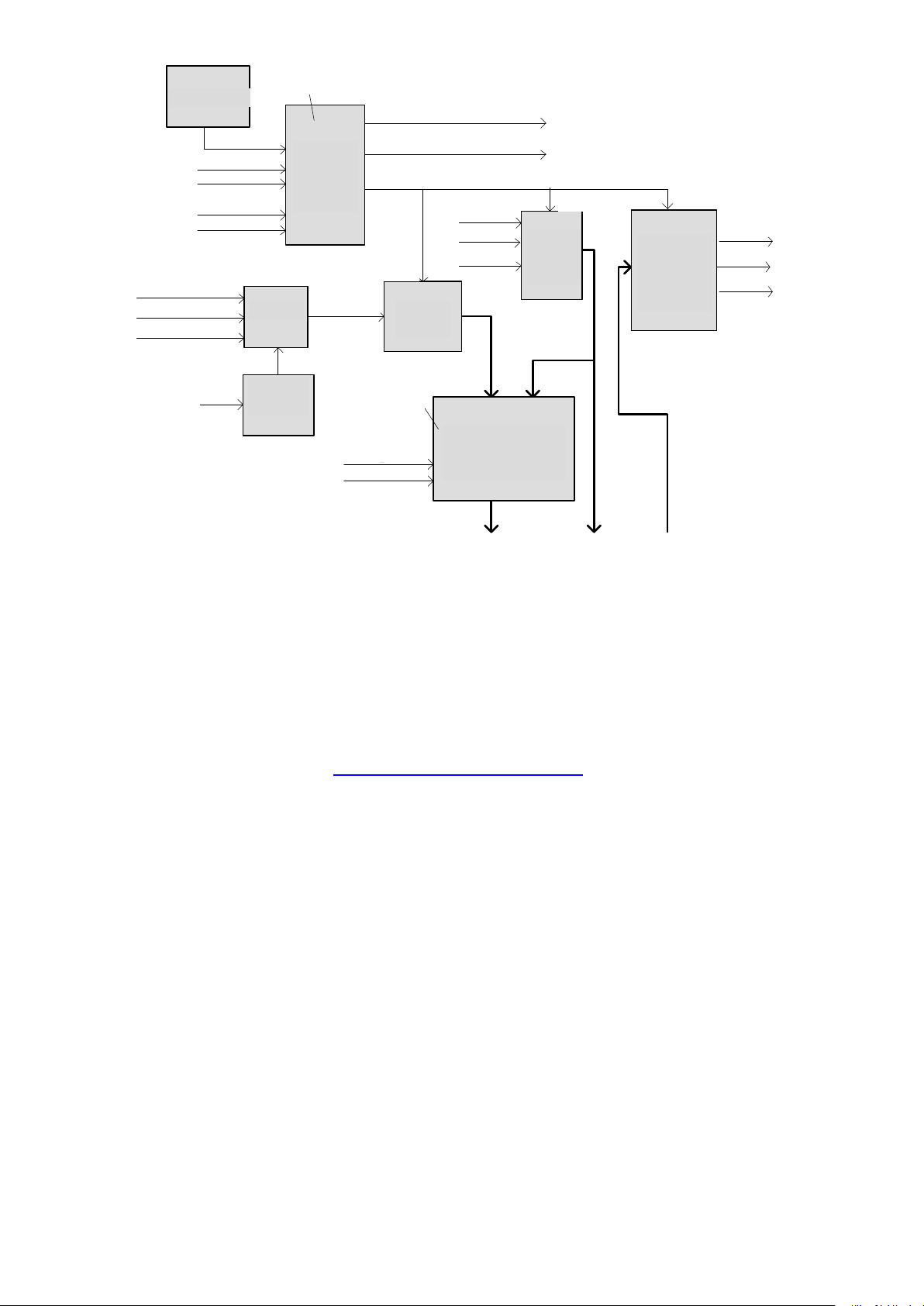
!
The functionality of the secondary synchronization is embedded in the project,
Узел
АЦП
Узел
ЦАП и
цифрового
вывода
Узел
цифр.
ввода
Комму-
татор
Схема
первичной
синхрони-
зации
E-502
Генератор
f
ref
f
ref
Общие условия синхронизации всех процессов ввода-вывода
в E-502 (выбор опорной частоты и условий старта)
DI_SYN1
DI_SYN2
DI_SYN1
DI_SYN2
CONV_IN
START_IN
START_OUT
CONV_OUT
К ведомому
E-502
От ведущего
E-502
Внешняя
синхронизация
DI_SYN1
DI1...DI16
DI_SYN2
Управля
ющая
таблица
DAC2
DO1...DO16
DAC1
Cхема вторичной
синхронизации
данных АЦП
Поток данных “на ввод” Поток данных “на вывод”
Синхр.
Синхр.
Синхр.
Синхр.
X1...X16
Y1...Y16
GND32
2.0 / 1,5 МГц
Вход Выход
I
II
Схема селекции
данных АЦП в
зависимости
от вторичных
условий
синхронизации
Data flow "to input"
To E-502
Scheme of ADC
DAC and
output node
Generator
Primary
E-502
ADC secondary
data scheme
Digital
node
Control
table
Switch
ADC
node
MHz
External
synchronization
From the master
General synchronization conditions for all I/O processes
Data flow "to output"
Output
Input
Synch.
Synch.
Synch.
Synch.
E-502
in E-502 (selection of reference frequency and start conditions)
slave
synchroniz
ation
scheme
data selection in
dependence
from the
secondary
synchronization
conditions
Fig. 3-2. Synchronization system structure in E-502
3.3.5.2. Secondary synchronization.
input
synchronization
digital
but is not currently implemented. You can find out about the availability of this
in the sales department of L-Card.
functionality
The se co ndar y s ync hro nizat io n circ ui t (II) is t he ADC data s electi on cir cuit depen ding on
the secondary synchronization conditions, operating exclusively against the background of the
previ ously started clock signal from the out put of the primary synchronization circuit (I) , i.e. aga in st
the back gr ound of t he star t ed dat a stream of th e ADC.
The fol l owin g ADC data r esol u tion s y nchroniza tion modes are supported:
• No syn c hroniza tion ( tr a n s pa renc y m od e)
• Synchronization from an analog signal in the selected ADC channel
• Digital synchronization with the selected signal from the inputs DI1 ... DI16, or
DI_SYN1, or DI_SYN2
he following modes of sensitivity to the fluctuations of the synchronization signal are
T
supported:
• Enable of ADC data on the e dge (drop) of an anal o g or di gi ta l signa l
• Enable of A DC d ata at a l evel "above the threshold" or "below the threshold" (for analog
synchronizati o n) or at the logic level "1" (for digit a l s yn c hr o nization)
The fol l owin g ADC data i nhi bit mod e s are supp or ted:
• Software p rohib ition (stop ) with the possibility of re-a uth o riz a tio n (if the p rev io usly se
e
nable condition is repeated) without restarting the primary synchronization scheme
t

• Automatic prohibit ion (stop) after entering the specified number of frames (from 1 to
32
-1 frames) with the possibility of re-authorization (if the previously set resolution
2
ondition is repeated) without restarting the primary synchronization scheme
c
3.3.6. Adjustment of the ratio between the time of setting the signal and the resolution for each ADC channel.
Above was the principle of the frame-by-line input of AD C data, which was applied in all LCARD ADCs with the input channel switch, up to synchronization frequency, frame size and
interfra m e de l a y. B u t i n L-502 and E-502 this principle is developed for the better adapta tion to the
output physical properti es of the signal source. Further we will discuss it more pr ecisely.
If E -502 is used at the highest possible data acquisi tion frequency from each channel, then set
= 1, whic h means that the samp ling period of one measurement channel is tsw = t
n
sw
only one AD C sa mple i s con vert ed. For exa mple, for f
=2 MHz t imet
ref
sw
= t
ref
short switching period of the channel switch, which imposes restrictions on the output impeda nce of
the signal sour ce (and t he wires from it): the impedance should be suffi ciently smal l (not mor e than
50 Ohm) and not have a large reac ti ve component, so that the duration of the transient proce s s caused
by circuit switching does not exceed 0.5 μs. In other words, the signal sourse should be no more than
50 Ohm and have a short or coordinated cable. For those who used the L-783, the se req ui reme nts and
these application conditions roughly correspond to the conditions of application of the L-783 in the
mult ich anne l mode at the m axim um AD C conv e rsion frequency of the 3 M Hz, b ut w it h the diff e rence
that the ADC resolution of the E-502 is 16 bits rather than 12, and the electronic switch in the E-502
is much more "qu iet" (i.e., injects significan tly less p arasitic ch arge into the signal circuit at the time
of commutation, and the ref ore causes a significantly smaller shock excitation for a pos sible t ransient
proces s in the signal circui t) .
But if it is required to use the E-502 at a data acquisition rate for each channel less than the
maximum, and it is possible to reduce the switching frequency, then in E-502 with internal
synchronization there is no reduction in the frequency of ADC startup, and n
as it is sh ow n in th e e xam ple on
fig. 3-1. But, in the sense of n
– this is the number of cycl es of
sw
> 1 is set, for example,
sw
ADC co nv ersi on f or one switching period. In the E-502 it is set by default that for n
read outs are flipped, except for the la st one, during t he switching period. It creates th e maxi mum
settling time a fter commutation (due to "idle" ADC conver sion cycles) , therefore the least stringent
requirements are imposed to the impedance of the signal source. On
fig. 3-3, with n
conditions ar e set "by default" for the logica l channel 1: the first two counts are always discarded,
and t he thir d one i s used. But th e real ta sks of using multic hannel ADCs do not assu me that the
impedances of the signal sources are the same, and for channels with connected low-impedance
sources it would be good not to discard at least some of the ADC samples, but to use them for
avera ging the data, thereby increa sing the ena ble when measuring t his channel. Such option is
provided for in E-502 due to the f act that in every ce ll of the cont rol tab le, besid es the phys ical channel
number, the re is als o th e ave ra g ing f acto r n
, by def aul t, nav= 1. Averaging factor nav ={1,2,…,128}
av
means: "how many counts of the ADC from the end of the swit ching cycle of this channel will be
used to a vera ging t he data ". Acc ordi ngly, n
= nsw - n
su
means "how many ADC c ount s from t he
av
begi nni ng of the swit chi ng cy cl e of th e giv en cha nn el wil l be di sca rd ed ", or "how man y peri od s t
will be used to set the sig nal at th e ADC in put a fter sw it chin g ".
For e xamp le, on
whi ch m ea n s tha t for n
fig. 3-3 f or na viga tional cha nnel 2 , n
=3 the result of the last two conversion periods in one switching phase will
sw
= 2 i s install ed in th e control ta ble,
av
be used fo r averagi ng, and one fi rst period is added to the time of s igna l est abli shme nt afte r swit ch ing.
For log ical channel 3, al l three samples of the ADC are used for ave raging, and the refore the minim um
time is assigned here to establish a signal after switching.
, during which
ref
= 0,5 μs is a fairly
>1, all AD C
sw
=3, such
sw
ref

1 2 13 2
Канал 1
Канал 2
Канал 3
t
k
nk=3
nd=2
t
d
t
k
t
ch
nsw=3
Кадр
Межкадровая
задержка
Кадр
Межкадровая
задержка
nav=1
nav=2
nav=3
nsu=2
nsu=1
n
su
=0
Номер
логического
канала АЦП
Момент сэмплирования одиночного отсчёта данных АЦП
Моменты сэмплирования отсчётов данных АЦП и выдача усредненного отсчёта
Отброшенный отсчёт данных АЦП
t
ref
t
sw
3
1
ADC logical
channel
Sampling time of ADC data single sample
Sampling time of ADC data and output of averaged readout
Discarded ADC data sample
Interframe
Interframe
Frame
Frame
Channel 1
Channel 2
Channel 3
number
delay
delay
Fig. 3-3. The pr inciple of obtaining ADC data (in detail)
fig. 3-3 it also follows that the set non-zero interframe delay actually increases the settling
From
ti me fo r the firs t lo gic al ch anne l. This can be used, for example, by associating the first logical channel
with t he physical channel to which the signal source is connected by the largest impedance.
It can be argued that by setting optimal n
optimize the timing of the signal conditioning associated with the inter-channel passage and the
resolution of the ADC.
It is i m p ortan t to no te t ha t i n th e E -502, the ADC averaging algorithm described here ( by the
simple avera ge me thod) is considered as an inseparable part of the ana log-to-digital converter itself,
alth ough p hy sicall y the a vera ging pr oc edur e is pe rform ed by mean s of F PGA u sing 2 4-bit inte ger
arithmetic.
random components of the si gnal of different nature, improves th e s ignal/nois e by suppressing
the hig h-fre quenc y compo nents o f the s pectr um abov e the Ny quist f requenc y of 0 .5*f
giv en ph ysic al ch anne l as socia ted wit h one (or more) logi cal cha nnel. No t e in pa ssi ng t hat di git al
filtering by the Blackfin processor (or high-level software) has a fundamentally different active
filte r ing area, bec ause it is below the Nyquist freq uency.
Such an averaging operation increases the real resoluti on of the ADC by suppressing the
Once ag ain , we emphasize that "by default" in the E-502 settings n
does not occur by default.
3.3.7. Relative switching dela y s in ADC channels.
where the magnitude of the relative signal delay between the ADC channels is important for
measuring relative phase delays. For this class of problems, the theoretical calculated latency values
in the ADC channels are taken into account in the delay equalizati on algorithm based on one or
This i nfor mat io n will be im por tant o nl y for t hat cla s s o f multi -channel data acquisitio n tasks
anot h er m et hod of si gna l interpolation.
/ nav settings for each channel, we are tryin g to
su
=1 is set, and "averaging"
av
for a
ch

For ADC mode without averaging (nav=1), the relative switching delay between adjacent ADC
chan nel s wit hi n one fr am e (in th e ord er o f polli ng th e con tr ol ta bl e) is equ al to t
last channel of the previous frame and the first channel of the next one i s t
If the averaging mode is used (n
>1 ) , w her e nav are select ed equal for all ADC channels, t he
av
absolute delay for each channel will decrease by the same amount 0.5*n
delay will remai n equal to t
between neighboring channels of one f rame and equal t
sw
sw
av*tref
, and between the
sw
+ td.
. Theref o re, the rel ative
+ td between
sw
the nearest cha nnels of neighboring frames separated by inter frame delay.
If th e a v er aging mode is u sed (n
>1 ), wh er e nav ar e assi g ned in the co n trol t a ble different for
av
i- and j-th logical ADC channel, the absolute signal delay on the i- channel will decrease by
0.5n
+ 0, 5* t
t
sw
av
(i)*t
, and the relative delay j channel towards the previous i- ( within one frame) becomes
ref
(nav(i)- nav(j)), or becomes equal to tsw + td + 0,5* t
ref
(nav(i)- nav(j)) b e tween the nearest
ref
i-th and next j-th chann els of n ei gh bor ing fra me s s epa rat ed by int er fra me dela y ( if mor e pr e cis ely,
for the last channel in the fr ame always i = n
, and for first, always j = 1).
k

3.3.8. Relative delays of the ADC, DAC and I/O channels.
Description
Desig-
Timing sample
Minimum
Typical
Maximum
Reference frequency period
t
500 ns (2 MHz)
Durat ion of the signal pulse CONV_ OU T
tW
50 ns
The delay time from the front CONV_OUT
t
0 ns
The time to set the state "1" to
t
45 ns
DAC1,
DAC2
CONV_OUT
START_OUT
DO
DI
1-ый отсчёт DO 2-ый отсчёт DO
Выборка
1-го отсчёта АЦП
3-ий отсчёт DO
t
REF
2*t
REF
2*t
REF
Выборка
2-го отсчёта АЦП
t
ADC
t
DI_SU
t
DI_H
Выборка
1-го отсчёта DI
Внутренний
преобразо-
ватель (АЦП)
Выборка
2-го отсчёта DI
1-ый отсчёт DAC1, DAC2 2-ый отсчёт DAC1, DAC2
3-ий отсчёт
DAC1, DAC2
t
DO
t
DAC
Выборка
3-го отсчёта АЦП
Выборка
3-го отсчёта DI
t
W
t
ST_SU
t
ST_H
X,Y,
GND32
t
ADC_SU
Sample
3rd ADC count
Sample
2nd ADC count
Sample
1st ADC count
Sample
3rd DI count
Sample
2nd DI count
Sample
1st DI count
1st DO count
2nd DO count
3rd DO count
3rd DAC1,
DAC2 count
1st DAC1, DAC2 count
2nd DAC1, DAC2 count
Internal
converter
(ADC)
Fig.3-4. Synchronous I/O diagram
In the above-mentioned s ynchr on ous I/O di agram , t he out pu t si gnal CO NV_ O UT is used as a
reference clock signal, with respect to which all I/O delays are described . Temp or al paramete rs of the
diagram are describe d in the table below. The delays in the ADC channel are given for the operating
mode without averaging the data and without allocating additional cycles of the ADC for setting the
signal
Group de lay time of anal og channel of ADC
channel in E-502
to the sampling time of the ADC chip
START_O UT be f ore the fro nt
CONV_OUT
(start of data col l ectio n)
nation
REF
t
ADC_SU
ADC
ST_SU
667 ns (1.5 MHz)
15-70 ns

Description
Desig-
Timing sample
Minimum
Typical
Maximum
Time of holding st ate "1" to
START_OUT after the front
t
150 ns
The time to set the da ta at the D I input
t
5 ns
Data hold time at the DI input
t
-1 ns
CONV_OUT
(terminati o n o f data coll e ction )
nation
ST_H
DO delay time relative to the front
CONV_OUT
The group delay time of the sig nal at the
output of th e DAC rel ative to the front
CONV_OUT
(delay of the DAC chip plus the delay of
the analog filter- buffer at the output of
the DAC)
DI_SU
DI_H
tDO
t
DAC
6 ns
2 µs

ARM
LPC4333/
4337
HOST
DMA
ADSP-
BF523
Порты
в/в
Схема
первичной
синхронизаци
и E-502
Схема
вторичной
синхронизации
данных АЦП
FPGA
Cyclone IV
АЦП
Комму-
татор
ЦАП
Цифровой
в/в
JTAG
X1...X16, Y1...Y16, GND32
DI_
SYN1
,
DI_
SYN
2
DO1...DO16
DAC1
, DAC2
Подсистема
ввода
-вывода
DI1...DI16
гальваноразвязка всегда
присутствует в E-502
Узел гальвано-
развязки
Только для E-502-P- -
Только для E-502- - -D
CONV_IN, START_IN
CONV_OUT, START_OUT
Функционально
близкая к L-502
часть
сбора/
выдачи
данных и
обработки.
Ethernet
PHY
Ethernet
Гальвано-
развязка
Ethernet
RMII
SDRAM
32 МБ
Только в модификации с Ethernet
Flash-память
2 МБ
USB
Reset
LED
1
LED2
Link
Activity
SDRAM
32 МБ
Интерфейсная часть.
AGND, DGND
GND
Цепи
изолированы
Interface part.
Only in the modification with Ethernet
Flash memory
SDRAM
Ethernet
isolation
Channel 3
I/O sub-system
O/I
ADC secondary
32 MB
E-502 primar y
scheme
there is always a galvanic
Functionally
close to the L
502 part of the
data collection/
transmission and
pro
Circuits are
isolated Only for
Galvanic isolation
node
Switch
Digital O/I
ADC
DAC
Only for
Channel 3
3.4. Operation principle and function circuit
synchronization
isolation in E-502
cessing.
E-502 operational scheme is nominally divided in two parts:
1. The part related to the collection/output of ADC/DAC data is dig ita l I/O. This part
2. E-502 interface part on the basis on LPC4333 (LPC4337) ARM controller, with
All E-502 modif icat ions have a LPC4333 (L P C4337) A RM cont rol ler and a galvan ic isol atio n.
synchronization
-
32 MB
2 MB
repeats the architecture of L-502. DAC and signal processor ADSP-BF523 presents
data scheme
Fig. 3-5. B lock diagram
ports
galvanic
depends on the E-502 modification. The FP GA is focused on the logic of data collection
control, the A DC c a li b ra tio n lo g ic, th e secondar y synchr oni zat ion l ogic (
3.3.5), and the
interface with the LPC4333 (LPC4337) ARM contr oller and the ADSP -BF523 signal
processor.
USB and Ethernet support. Ethernet option depends on the E-502 modif ication.

Flash-memory with a capacity of 2 MB is desi gned for stor ing FPGA firmwar e, calibration
factors, factory serial number. Half the amount of Flash memory is provided for user tasks.
The E-502 I/O subsys tem (in par t 1.) contains nodes for the channel sw it c h, ADC, DAC, digital
I/O, as well as the primary synchroni zation circuit (
3.3.5).
A galvanic isola tion node isolated all cir cuits of the I/O sub system from circuits electri cally
connected with any other circuits.
Signal processor ADSP-BF 523 with S DRAM 32 MB is des igned fo r add itio nal d at a proce ss ing
and mana gement within user tasks. If the processor is enabled, the entire data stream and the I/O
subsystem are tran sferre d thr ough t he pr oce ssor' s I/O port s. For exa mple, it i s possi ble t o cr eate a
con trol loop th rough a sign al process or using al l the cap abilities of E-502 data coll ection and delive ry.
Independent processor a nd data transfer Interface is performed through the HOST DMA processor
port t o the ARM -controller. The processor has a JTAG connector on the board.
ARM controller LPC4333 (LPC4337) has it s
independent SDRAM 32 MB and hidden R eset
button, located on the E-502 front panel. The test of this SDRAM is always done after the power
is turned on (the error is indicated by LED2, s. 2.3.2, p. 14).
P
rocessors LPC4333, LPC4337 are identical, in terms of their resources involved, and the
option of bundling does not affect the consumer properties of the product
1
. ("L-Card"
The manufacturer reserves the right to optionally complete the E-502 module either with the
LPC 4333 or LPC 4337 p rocess o r without any dist inct ive pr od uct ma rking and without corr espond ing
differences in product passports.
A short press of the Reset but ton makes a normal reset of the AR M controller.
A long press (more than
10 s) of the Reset button (s. 2.4, p. 14) shifts the E-502 to a special
"loader" mode via USB. A special mode is needed to update the E-502 firmware and change the
Ethernet IP address.
A
fter power supply is applied to the E-502, the f irmware will be dow nloaded to the FPGA from
the Flash memory (
fig. 3-5), and the E-502 in ternal power s upply system will be fully turned on, after
which the E-502 will be ready for norma l operati on.
E-502 swit ches to work with USB or Ethernet after tur ning on t he po wer au t omat ica ll y on the
interface from which the first access to the E-502 will take place. Parallel operation from both
interfac e s is n ot supported.
1
distinctive product marking and without corresponding differences in product passports
"L-Card" reserves the right to optionally equip the E-502 module with either the LPC4333 or LPC4337 processor without any

3.5. All functional differences of E-502 and L-502.
PCI Express card (installed
The function of the inputs DI15,
DI16 is combined with the function
module synchronization
inputs CONV_IN, START_IN,
input of
external synchronization
up resistor of
resistor of DI digital
502 modifications
mode for output to the
Is supported by PC software
502, a data buffer 2 pages of 1.5
Functional difference L-502 E-502
Structure
ins ide the PC )
External module in relation to the
PC.
Int erfa ce wi th the P C PCI Express 1.0 USB 2.0
Ethernet (100BASE-TX)
Intermodule
synchronization interface
Uses a different connector.
CONV_IN, ST ART_ IN in puts
Has a singl e Digital c onnector wit h
digital I/O sig nals.
have constant pull-up r es istor s
to "zero ".
of the inter-
respectively.
DI15/CONV_IN, DI16/START_IN
inpu ts ha ve di ffe rent pr og ram ma bl e
pull-up resistors to "zero" (s.
34).
p.
The second 2
DI_SYN2
Is present separately on the
internal connector L-502.
Progr a mma ble pul l-u p r esi stor
Is combined w it h D 14 input.
Programmable pull-
DI14/ DI_SYN2 input
of DI_SYN2 input
4.4.2,
Programmable pull-up
Is present (separate for the high
and low byte)
inputs
Galvanic isolation Not all E-
hav e i t
Cyclic self-oscillator
driver.
DAC and digital output.
C
omparing to L-502, i n E-502 DAC meteorological characteristics have been improved (s. 5.2)
while reproducing direct and alternate current voltage.
No
All E-502 modifications have it
Is supported by the interface ARM
con tro ller L PC4333( 4337) within E-
Mcounts.
2
E-502
The first external clock input DI_SYN1 is available on the external connector in the L-502 and on the Analog connector in the
)

(f iguratively: G2). Thes e ci rcuits are connec ted to the common wi re of the ARM con troller and
AGND
DGND
GND
0V
CHASSIS
GND_USB
Фильтр
Гальванический
барьер
G2
G1
Galvanic barrier
Filter
Chapter 4. Connection of signals.
This section contains information on E-502 connectors, their contacts' purpose and main
characteristics of E-502 inp uts and out puts, related to the c urrent connection.
4.1. DGND, AGND circuits
AGND is a commo n wire circuit of isol ated analog circuits : ADC inputs and DAC outputs.
DGND is a common cable circuit of isolated digital circuits: digital inputs and outputs.
Inside the E-502, the AGND and DGND circuits have a common connection point
!
(figuratively: G1 ), but th ese cir cu it s are is ola t ed fr o m GND , USB m E t her ne t and E-502 power
input (
4.2. GND, 0 V, GND_USB, CHASSIS circuits
GND is a common w i re circuit of digital nodes of E-502 module in the non-isolated part.
0 V is a circuit of the zero potential of the low-voltage E-502 power input.
GND_USB is a common wire circuit of USB interface.
CHASSI S is a c ircui t f or chas sis connect ion ( onl y i f E-502 is us ed wi thout cover – for embedded
application) and signal cables display
!
Inside E-502, GND, 0 V, GND_USB, CH ASSIS circuits have a common connection point
fig. 4-1)
4.3. Location of DGND, AGND, GND, 0 V, GND_USB, CHASSIS circuits on the board
schematically their belonging to different functional parts of the E -502.
the non-is ol a ted USB interface (fig. 4-1).
Fig. 4-1: Internal connection of the "common wires" circuits in E-502.
In sub it ems 4.1 and 4.2the purpose of these circuit s is explained, and the figure below shows

1
JTAG Blackfin
(GND)
JTAG ARM
(GND)
1
1
UART
(GND)
ADSPBF523
FPGA
Cyclone
IV
SDRAM
SDRAM
ARM
LPC4337
CPLD
USB
(GND_USB)
D I G I T A L
Элементы
ЦАП
A N A L O G
Гальванический
барьер
Отв. 3,05 мм
GHASSIS
Корпус
разъёма
(CHASSIS)
Корпус
разъёма
(CHASSIS)
Цифровые
сигналы
(DGND)
DI_SYN1
(DGND)
Aналоговые
сигналы
(AGND)
Изололированные
входы Ethernet
GHASSIS
Отв. 3,05 мм
GHASSIS
0 V
DAC
elements
Digital signals
Port Ø3,05 mm
Port Ø3,05 mm
Connector
Isolated Ethernet
Galvanic barrier
Connector
chassis
Analog
signals
chassis
inputs
Fig. 4-2: The locat ion of the "common wires" circuits on the E-502 board
In particular, GND is a common wire for internal interfaces UART, JTAG Blackfin, JTAG
ARM.
If you use a sep arate E-502 board without a chassis
(CHASSIS), it is recommended to connect it to the solid metal surface of the chassis (case
cons truct ion). Two ri ght por ts of 3.05 mm on fig. 4-2 have a metal co at ing c onnec ted to a CHASSIS
3
in the emb edde d ch assis circuit applications
circu i t, and t w o left ports o f 3.05 mm are isolated from the other circuits. These 4 mounting ports
are used to secu re the E-502 board.
4.4. E-502 connectors description
4.4.1. Connector Analog.
Connector Analog is a 37-pin 2-row type DRB-37M plug on the front panel of the E-502. The
conductive connector contact piece (shield) is electrically connected to the GND signal ground
circuit. On the shield of the cable part of the conne ctor, the shield of the signal c able can be direc tly
sealed. The c onne ctor Analog shi el d doe s not ha ve a con tact wit h AGND , DG ND and oth er cir cui t s
of the Analog connector.
3
Here we do not consider the usage accuracy of the certified Measuring Device without a standard chassis.

Signal name
Commo
Direction
Description
X<1…16>
AGND
Input
recommended to be connected to
Y<1…16>
AGND
Input
recommended to be connected to
1
20
2
3
4
5
6
7
8
9
10
11
12
13
14
15
16
17
18
19
21
22
23
24
25
26
27
28
29
30
31
32
33
34
35
36
37
X16
X15
X14
X13
AGND
DAC1 / +15V / AGND / NC
Y2
Y1
GND32
DI_SYN1
X12
X11
X10
X9
X8
X7
X6
X5
X4
X3
X2
X1
Y4
Y3
Y6
Y5
Y8
Y7
Y10
Y9
Y12
Y11
Y14
Y13
Y16
Y15
DAC2 / -15V / DGND / NC
GND
Table 4-1: Connector Analog
4
The common wire circuit for the specified signal input or output
n point4
g. 4-3: Connector Analog
Fi
• Non-inverting channel voltage input 1 ... 16 for differential and
"common ground" mode:
•
Operation voltage range: ±10 V (see the details in section 4.6 p. 41).
• Unused inputs X <1 ... 16> are
AGND or the cor respond ing phy sic a l cha nnel not t o be inte rrogat ed
programmatically.
• Inverting channel voltage input 1 ... 16 for differe ntia l mode.
• Input channels 17 ... 32 for the mode "wit h common ground".
•
Operation voltage range: ±10 V (see the details in section 4.6 p. 41).
• Unused inputs X <1 ... 16> are
AGND or the cor respond ing phy sic a l cha nnel not t o be inte rrogat ed
programmatically.

Signal name
Commo
n point4
Direction
Description
DAC1
2.2.1
AGND
Output
For modif icati ons, E-502-░-░-D can be configured with a jumper as
DAC2
2.2.1
AGND
Output
For modifications, E-502-░-░-D can be confi gur ed with a jumper as
AGND
— — Analog gr ound
GND32
AGND
Input
DI_SYN1
DGND
Input
Synchroni zation input 1, which can also act as an additional input to
/ +15 V
/ AGND
/ NC
(see section
)
/ -15 V
/ DGND
/ NC
(see section
)
the output of the 1st channel of the D AC (voltage output in the
range -5 .. . + 5 V).
For any modificati ons, the E-502 can be configured with a jumper as +
15 V output of an externa l device, or as an additional A GN D contact, or
as an unconnected contact of the connector (NC).
(see section 2.2.1)
the output of the 2nd channel of the DAC (voltage output in the
range -5 ...+ 5 V).
For any modificati ons, the E-502 can be configured with a jumper as 15 V output of an externa l device, or as an additional A GN D contact, or
as an unconnected contact of the connector (NC).
(see section 2.2.1)
• In the "with common gr oun d" mode: common inverting channel input
1 ... 32.
• For a ll modes must be connected to AGND (in differential mode - to
increase noise immunit y). In the "with common ground" mode , t he
connection to AGND is recommended to do on the signal source side.
• Operation voltage range ±1 V (see the details in section 4.6 p.41).
the digital input.
Compatible with the output logic level of TTL/CMOS- cells with a
supply voltage of +2.5 V to +5 V. The input has an extended range of
maximum permissible voltage s (± 10 V r elative to GND ) .
The minimum rate of rise of the signal drop at the input DI_ S Y N1 is
not specified, since there is a Schmitt trigger on this input.
There is a software option to turn the 1k pull-up re si st or to a high logic
level at this input.
The DI_SY N1 input does not bypass the external TTL source, even
when the power is off.
Notes to table 4-1:
• The maximum perm issible voltages and currents at the contacts of the connectors are indicated in section
4.5, on p.40.

4.4.2. Connector Digital.
1
20
2
3
4
5
6
7
8
9
10
11
12
13
14
15
16
17
18
19
21
22
23
24
25
26
27
28
29
30
31
32
33
34
35
36
37
DI16 / START_IN
DI1
DI2
DI3
DI4
DI5
DI6
DI7
DI8
DI9
DI10
DI11
DI12
DI13
DI14 / DI_SYN2
DI15 / CONV_IN
DGND
CONV_OUT
DO16
DO1
DO2
DO3
DO4
DO5
DO6
DO7
DO8
DO9
DO10
DO11
DO12
DO13
DO14
DO15
DGND
+3,3 В
START_OUT
Connector Digital is a 37-pin 2-row plug of DRB-37F type on the E-502 front panel. The
conductive connector contact piece (shield) is electrically connected to the GND signal ground
circuit. On the shield of the cable part of the conne ctor, the shield of the signal c able can be direc tly
sealed. The Digital connecto r s hiel d ha s n o c ont act w ith th e D GND c irc uits an d the rem ainin g c irc uits
of the Digital connector.
Fi
g. 4-4: Connector Digital

Table 4-2: Connector Digital
DI14/
DGND
Input
Input
Digi tal input DI14 or synchr onization input D I_S Y N2
DI16 /
DGND
Input
Input
Digi tal input DI16 or synchr onization input START_IN
DO<16…1>
DGND
Output
Z-state
16-bit digital output, where
2.2.2.
CONV
DGND
Output
Output
The output of the ADC-DAC conversion pulse and the
START
DGND
Output
Output
The output of the ADC-DAC start signal and the I/O (to
DGND
— — —
A "common wire" circuit for digital i nputs and outputs.
Signal name
DI<13…1> DGND Input Input 16-bit digital input, where
DI_SYN2
DI15 /
СONV_IN
Commo
n point
DGND Input Input Digital input DI15 or synchr onization input CONV_ IN
Direc-
tion
State after
connection
Description
DI1 is the low bit, DI16 is the high bit of the 16-bit
word. The inputs DI14, DI15, DI16 a re described bel ow,
they have alternative programmable functions for the
synchronization inputs. The DI input does not bypass the
external TTL source, even when the E-502 power is off.
(software selection). The input is compatible with the
output logic level of the TTL/CMO S - cells with a supply
voltage of +2.5 V to +5 V. There is a Schmitt trigger at
this i nput. There is a software opti on to turn the 1k pullup resistor to a high logic level at this input. The
DI/DI_SYN 2 input does not bypass the e xternal TTL
source even when the E-502 power is off.
(software selection). Input of the synchronizati on pulse
of the A DC-DAC conversion (fro m t he neighboring
module E-502). It is program mable to turn on a pull-up
resistor of 360 ohms to a low logic level at this input.
The DI15/СONV_IN input does not bypass the external
TTL sourc e, even with the E-502 power off. The input is
compatible with the output logic level of the
TTL/CMOS- cells with a supply voltage of +2.5 V to +5
V. There is a Schmitt trigger at this input.
START_IN
_OUT
_OUT
(software selection).
Input of start signal of ADC-DAC and input-output
(from neighboring module E-502). Active logical signal
level is high. It is progra m ma ble to turn on a pull-up
resistor of 360 ohms to a low logic level at this input.
The DI16/START_IN input does not bypass the exte rnal
TTL sourc e, even when the E-502 power is off. T he
input is compati ble with the out put logic level of the
TTL/CMOS- cells with a supply voltage of +2.5 V to +5
V. There is a Schmitt trigger at this input.
DO16 – high bit , DO1 – low bit of the 16-bit word .
Lines DO1 ... DO8 refer to the low byte, and lines DO9
... DO16 - to the high one. Program control Z- state is
ind ependent for the high and low bytes. It is possible to
force the active st ate of the out puts of each byte when
the power is turned on by installing jumper, section
I/O (to t he neighboring E -502)
the adjacent E-502 module).
Active logical signal level is hi gh.

Signal name
Commo
Direc-
State after
+3.3 V
DGND
Output
Output
Output +3.3 V supply external digit al nodes.
n point
tion
connection
Description
F
section
+3.3 V
Short circuit of the +3.3 V circuit is undesirable, but
permissible (causes heat protection of the internal
stabilizer).
or the maximum permissible voltages and currents at the contacts of the connectors, see the
4.5
, on p. 40.
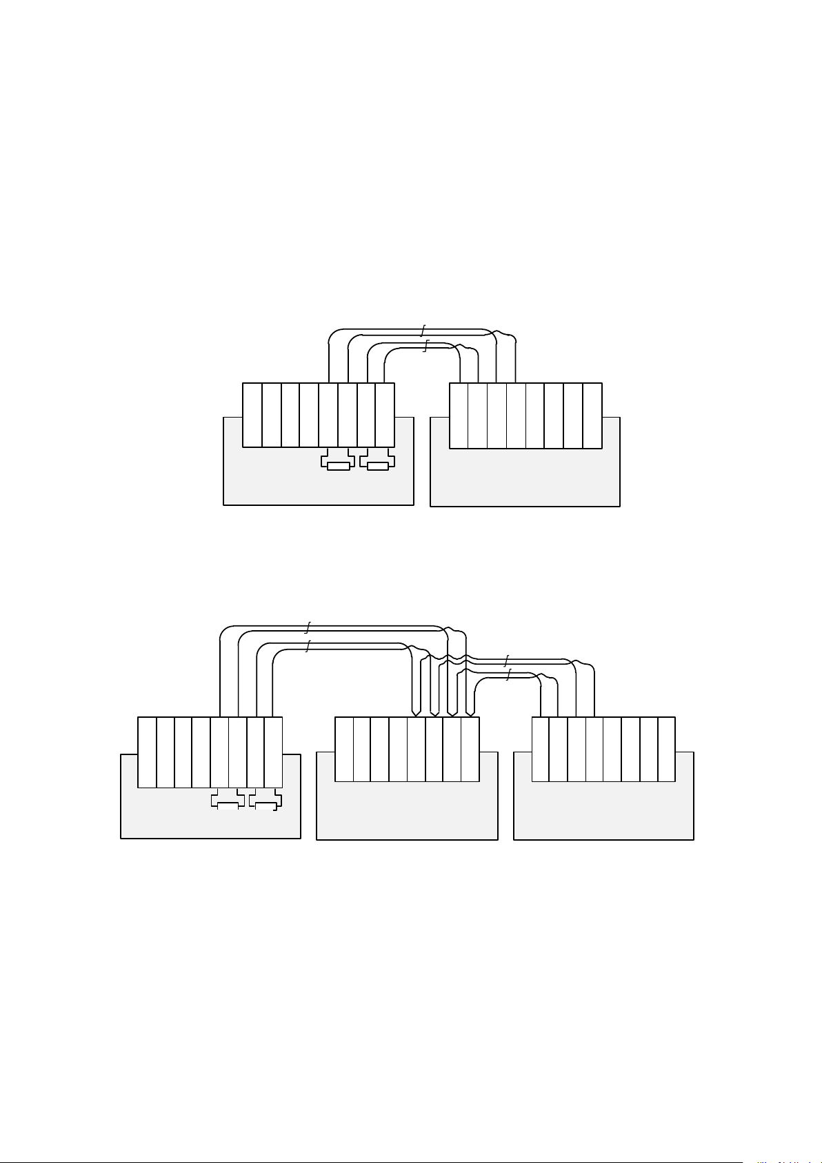
4.4.2.1. Connections with intermodule synchronization.
CONV_OUT
START_OUT
CONV_IN
DGND
DGND
START_IN
DGND
DGND
CONV_OUT
START_OUT
CONV_IN
DGND
DGND
START_IN
DGND
DGND
E-502 #1
(ведущий)
E-502 #2
(ведомый)
CONV_OUT
START_OUT
CONV_IN
DGND
DGND
START_IN
DGND
DGND
CONV_OUT
START_OUT
CONV_IN
DGND
DGND
START_IN
DGND
DGND
CONV_OUT
START_OUT
CONV_IN
DGND
DGND
START_IN
DGND
DGND
E-502 #1
(ведущий)
(ведомый)
E-502 #2
E-502 #3
(ведомый)
(slave)
(master)
(master)
(slave)
(slave)
Examples of connections with inter module synchronization are shown on
fig. 4-5 – fig. 4-7.
Connections shoul d be made with shortest twisted pairs for a number of E-502 mod ules located next
to each other.
The softwar e of such a system should ensure the start of data collection of the master modul e
after the slave star ts and pre-programmed these modules to the appropriate synchronization modes.
It is needed t o programmatically turn on the pull-up resistors on the inputs START_IN and
CONV _IN to a low log ic lev el on the l ast sl ave mod ule in the circ uit. It is recomme nded th at no mo re
than 2 adjacent slaves ar e connected to the same chain with the master. Each slave in the cir cuit, f or
exa mple, E -502 #2, as it is shown on
fig. 4-7, can, if necessary, become the master for the other
sync hroniza tion circuit.
g. 4-5: Synchronization scheme master - slave
Fi
g. 4-6: Synchronization scheme master - two slaves
Fi

CONV_OUT
START_OUT
CONV_IN
DGND
DGND
START_IN
DGND
DGND
E-502
#3
CONV
_OUT
START_OUT
CONV_IN
DGND
DGND
START_IN
DGND
DGND
CONV
_OUT
START_OUT
CONV_IN
DGND
DGND
START_
IN
DGND
DGND
E-502 #1
(ведущий)
(ведомый для #1,
ведущий для #3, #4
)
(
ведомый)
CONV_OUT
START_OUT
CONV_IN
DGND
DGND
START_IN
DGND
DGND
E-502 #4
(
ведомый
)
E-502 #2
Цепь 1
Цепь 2
DI1...DI8
DO1...DO8
DI9...DI16
DO9...DO16
8 бит
8 бит
E-502
8 бит
(slave for #1, master
for #3, #4)
(master)
Circuit 2
Circuit 1
(slave)
(slave)
8 bits
8 bits
8 bits
Fig. 4-7: Example of a two-circuit synchronization scheme
4.4.2.2. What gives an independent resolution to the outputs of the high and low byte?
One of the i mportant practical examples is a system of 3 buses with a width of 8 bits each, as
shown in the f igure below. The first bus is the input one, th e second is the output bus, the third is bidirectional.
that have an 8-bit bidirectiona l data bu s , i n pu t an d ou tput control lines. It shoul d be noted that DI14,
DI15, D I 16 inputs have alternative sy nc hroniz ation functions (
Fig. 4-8: Example of a groupe d c onnection of digital lines : three bu ses of 8 bits e ach.
The example shows an almost important case of impleme nting interfaces with various devices
table 4-2).

4.4.3. JTAG connectors of Blackfin processor.
emulator connector should be done in
Do not connect the JTAG connect or to other devices which ar e not specified in this chapter.
GNDBF_EMU
TMS
TCK TRST TDI TDO
BTMS/
VDDIO
GND
GND
GND GND
RESET
TDO
3.3V
TCK
TMS
TDI TRST
3.3VGND
GNDGND
GND
GNDGND
GND
RTCKGND
3.3V
TXD
RXD
2
4
6
8
10
12
14
5
1
7
9
13
11
1
2
3
4
1
2
3
4
5
6
7
8
9
10
11
12
13
14
15
16
GND
JTAG Blackfin
JTAG ARM
UART0 ARM
To debug your own Bla ckfin s o ft wa re on th e E-502 board, you should use one of the
JTAG- emulators from Analog Devices: ADZS-USB-ICE , AD ZS -HPUSB-ICE or
ADZS-ICE-100B with the USB-interface. They differ significantly with USB transfer rate and
price. You can get information on these devices on the manu fa ctur er's w eb site www.analog.com
The boa rd ha s a JT AG co n nector , fig. 4-9, compatible with the above JTAG- emulators.
The operation of attaching and detac hi ng t he J T AG the de-energized state of both devices.
!
.
Fig. 4-9. Detailing of signal s on JTAG B lackfin JT AG ARM and UART0 connect or s
4.4.4. Connectors JTAG and UART0 of the ARM controller LPC-4333 (LPC-
4337).
To debu g you r o wn Bla ckf in so ftwa r e on the board , you pr oba bly wil l not n e ed to mo dif y the
ARM-controller software that performs the interface function E-502. However, for advanced u sers
such a mo difi ca tion is p o s si ble, for example, in order to use the U A R T 0 ARM po r t f or any int erface
functions.
It is also shown on fig. 4 -9 th e standar d JTAG pinou t for ARM , as well a s the pinou t for th e
UAR T0 ARM interf ace ( the loc ati on of the con nec tors on fig. 4-9 corr espo nds to thei r actual rel ative
position in the E-502).
The TXD and RXD signals of the UART0 interf ace have an internal pull-up to 3.3V by resistors
of 10 kΩ.
The operation of connection and disconnection the JTAG-emulator and UART0 connectors
should be done in the de-energi z ed state of the connected devices.

4.5. The maximum allowable conditions at the inputs
!
Circ uit/ Signal
Maximum permissible modes description
Output s +1 5 V, -15 V
No more tha n 30 mA in load circuits when the total load
Inputs DI_SYN1
± 10 V relative to the DGND circuit with an internal input
Digi tal inputs of dual purpose DI14 /
From -0.4 to +3.6 V relative to DGND circuit
DO digital outputs
From -0.4 to +3.6 V relative to the DGND ci rcuit, the
TX, RX signals on the internal UART0
From -0.2 to + (Vcc + 0.2) V relative to the GND cir cuit,
Maximum permissible through-current by the
Maximu m permissible through-c urr ents by circuits
The maximum permissible voltage rise rate
10 kV / μs
and outputs of signal lines.
Under the maximu m permissible conditions are meant such currents and voltages that do not
lea d to fail ur e or irr ever si ble d egra dati on o f the ch ara cter isti cs of t he E-502. At the same time, the
max imum p ermi s sible cond i tion s ma y not pr o v i d e t h e per fo rman c e char a cteri s t ics o f the pro duct.
Long-term op erati o n o f e quipment a t ma ximum permis sibl e level s is not allow ed
Table 4-3 Maximum permissible E-502 input/output conditions
Inputs X1÷X16, Y1÷Y16, GND32 ±15 V relative to AGND
Outputs DAC1 , DAC2 ± 20 mA when the total load power is not exceed ed, se e
section
power is not exceeded , see section 4.8
SC is not pe r mi tted.
4.8
resistance of, at least, 1 kΩ.
Digital inputs DI1÷ DI13, DI_SYN2 From -0.4 to +6.5 V relative to the DGND ci rcuit
DI_SYN2, DI15 / СONV_IN, DI16 /
START_IN
current is not more than ± 20 mA. When the power is on, the
total load power should not exceed the calculat ed value,
4.8 .
connector
according to secti on
where Vcc is the E-502 internal voltage of 3.3 V .
The load current is not more than ± 8 mA.
Table 4-4 Maximum permissible through currents by common wires ci r cuits:
circuits of one E-502 module:
AGND-DGND5
100 m
A
GND, 0 V, GND_USB, CHASSIS
(on any contour into which covers these circuit s) 100 mA
between galvanically isolated circuits in E-502
The maxi mum p ermis sible circuit
scope of application of JTAG is limited to the standard types of JTAG emulators and the
specified connection procedure, according to i. 4.4.3, p. 39.
5
The notio n of circuits GND, AGND, DGND is introduced in s ection 4.1
modes of JTAG connectors are not considered, since the

4.6. ADC input operation voltage range
X
i
Y
i
GND
E-502
Измеряемое напряжение ±10 В или ±5 В
в зависимости от установленного
поддиапазона
Постоянное или переменное напряжение
смещения в диапазоне ±1 В
относительно GND.
Режим “дифференциальный” ±10 В или ±5 В
Режим “с общей землёй”
Измеряемое напряжение
от ±0,2 В до ±10 В в зависимости от
установленного поддиапазона
Измеряемое напряжение ±2, ±1,
±0,5 или ±0,2 В в зависимости от
установленного поддиапазона
Постоянное или переменное
синфазное напряжение (Uxi +Uyi )/2
в диапазоне ±1 В.
Режим “дифференциальный” ±2, ±1, ±0,5 или ±0,2 В
Постоянное или переменное
напряжение смещения GND32 в
диапазоне ±1 В.
U
Yi
U
Yi
U
Xi
-
U
Yi
X (Y )
i
GND32
GND
E-502
U
Xi(Yi)
-
i
U
GND32
U
GND32
X
i
Y
i
GND
E-502
U
Yi
U
Yi
U
Xi
-
U
Xi
Measured voltage ±10 V or ±5 V, depending
on the set subband
Measured voltage ±2, ±1, ± 0.5 or
± 0.2 V de pending on the set subband
Constant or a lternat ing common-mode
voltag
Constant or alternating offset voltage U y; in the
range of ± 1 V relative to GND .
Measured voltage from ±0.2 V to ±10 V,
depend
Constant or alternating offset voltage
GND32 in the range of ± 1 V.
Differe ntial mode ±2, ±1, ±0,5 or ±0,2 V
Diffe rential mode ±1 0 V or ±5 V
Mode "with common ground"
Note that in the differential mode on the sub-bands ±10, ±5 V, the E-502 has unbalanced input
and output ranges for the inputs X and Y with respect to the AGND analog ground circuit, and in the
"common ground" mode, the E-502 on the same subbands ha s asymmetrical input signal ranges of
the inputs X (Y) and GND32 wi th regard to the AGND c ircuit.
ing from the set subband
The figure below shows exa mples of connecting voltage sources (VS) to the ADC inputs.
Z, Z1, Z2 - th e i nt r i nsic r e si s t a n c e s of the wires ( t hroug h w hich t he through cur rent s ca n f low
with the connection of different devices) or other external electrical causes inducing the parasitic
offset voltag e U
e (Uxi + Uyi)/2 in the range ±1V.
, UYj.U
Yi
are indicated. In the first two ci rcu its, the vol ta ge UYi, UYj should not
GND
exceed ± 1 V in order to ensure the operating mode, and in the latter scheme the common mode
voltage ( U
Xi +UYi
)/2 must be within ± 1 V.

X
i
Y
i
GND
E-502
Z1
U
Yi
GND
E-502
Z
U
Yi
GND32
X (Y )
i
i
Дифференциальный ИН
и дифференциальный. реж им L-502
X (Y )
j
j
GND2
GND1
Z2
X
j
Y
j
GND1
U
Yj
От дал ё нны е одн о ф азн ы е ИН и диф ф. реж им L-502
Отдалённая группа однофазных ИН
и ре ж и м с “общей землёй” L-502
Дифф. ИН
X
i
Y
i
GND
E-502
U
GND
Z
U
Yi
U
Xi
Differential VS
and differential mode L-502
Remote single-phase VS group and "w it h
common ground" mode L-502
Remote single-phase VS and diff. L-502 mode
Diff. VS
Examples of connecting
the ADC input are collected in the item 6.1 on page 54.

4.7. Preconditions for correct connection and correct
... if you do not take into acco unt t he elec tric al prope rties of the sign al so urces , wires (c ables )
502 progra m settings, then, most
settings of the input of the ADC E-502.
Simplified exampl es of connection of the ADC input are given in section 6.1, however,
when using E -502 ADC connections, use the default Elikely, you will get a bad result. Why? What do you need to consider? – If y ou answer be low
!
these questions, links to the In ternet resources of the site
4.7.1. The physical causes of possible problems
Physical cause #1. The wide bandwidth of ADC transmission in E-502 (ab out 10 MHz) can
be not only a big a d va nt age o f AD C E-502 (i n t h e a bili ty o f the ADC to qualitati ve ly d igi ti z e hi ghspee d d ynami c proces s e s), but it can be a big problem i f:
• th e signa l sou rc e ha s an unli mit edl y wid e fr equ enc y ban d (muc h wide r tha n th e widt h
of the frequencies of the useful s ignal)
• unscreened connection is applied (or the signal source itself ha s a significant area of
the unscreened surface), in a situation where elect romagnet ic fields in the frequency
band up to 10 MHz are always pres ent in the real situat ion, and also in the situati on of
the user' s fai lu re to appl y a differential connec tion (an d adjustme nt to the differe ntial
mode), and therefore use the valuable property of a differential input – effectively
sup pressing co m m on -mode interference.
Physical cause #2. The high frequency of the 2 MHz channel switch ( when tuned to multichannel mode) with E-502 default s ettings m ay not only be a big advantage of the AD C E-502 (i n the
high-speed ADC input interrogation), but it can also be a problem because of the measuring circuit ,
it takes a short si g nal s ettin g ti m e (l es s than 5 0 0 n s a fter t he sw it ch' s o wn c harg e i s inj e cte d into the
measur ement circuit). This cause is funda mental for all ADC with input commutator, manifested a s
a switching disturbance.
en.lcard.ru will be used.
4.7.2. Conditions for correct E-502 connection and settings.
1. If you need to use no more than 16 ADC channels, always select the differential
connection m ode and E-502 settings.
2. With a di fferential connection, the X and Y circuits of each channel always lead in pairs
(twisted pair, sh ielded pair).
3. E-502 signal circuit should be shielded. On t he screen connection, see
4. For differe ntial co nnect ion, when usi n g a pa ir ca b le, to ma ximiz e th e c o m mon-mode
rejection of the E-502, the output impedances on the side of the remote source along the
X and Y c ircuits must be balanced (connection ex amp le - p.
5. The AGND E-502 circuit should be connected to t he common wir e circuit of the signal
source (if there are several signal sources – to the common junction poin t of the signal
source common wires).
6. If you need t o c on f igure th e E-502 for multic hannel ope r a tion, you first need to optimize
the signal-to-noi se ratio of the ADC in a single-channel operation mode with a
maximum dat a rate of 2 MHz, in which in the sign a l spectr um you will see all the
fre quencie s of the in terfering interfe re nce (pos sibly with "mir ror frequenci es" if
interfer e nc e is abov e 1 MH z), whi c h m ea ns that you ha ve a tool in your hands to find the
6.1.9).
4.4.1.

sources and causes of these interfe re nces (before switching to multi-channel mode and
averaging mode, when it is more diffic ult to understand the sources of inte rference).
7. When using ("by default") in the multi-channel operation mode of the maximum
switching frequency (2 MHz), the output impedance of the E-502 signal circ uit must
be from 0 to 50 Ω (in the frequency band up to 10 MHz), and this voltage source
must be connected to connect or E -502 by wi r es of zero length. This is achieve
e
ither by directly connecting the output of the signal source itself (50 Ω) or b
d
y
connecting its load resistor (up to 50 Ω) directly to the cable part of the E-502 signal
connector (cases of connecting a 50 Ω coherent line or a current shunt to 50 Ω of the
external current m easur e ment circu i t).
8. When using a multichannel mode of non-zero length of wires to the voltage source
and (or) with an output resist ance of the signal ci r c uit of more than 50 ohms, the
program set ting of the s ignal conditioning time n
9. I n multi-channel mode, the optimal settling time n
> 1 (s.3.3.6) should be appli e d.
su
(s. 3.3.6) should be selected
su
depending on the output impedance of the signal source, the length and the
coherence of t he cable. It is suggested to choose the opt imal n
for this channel by the
su
crit er i o n of obtaining a s ma ll inter-channel signal transmission fr om the pr evious polling
channel.
10. To improve the signal-to-noise ratio and increase the resolution in the
measurement path, it is recommend ed to use the maximum poss ib le averagin g
factor n
signal conditioning t ime n
11. D o no t exceed the operating voltage rang e s a t the inputs X, Y, GN D 32 (s.
12. Use the E-502 "with common ground" operation mode only i n case of closely locate
w-resistance signal sources. Optimizing the n
lo
ou nd " m o de is requ ired. D o no t ma k e " c om m on grou nd" co nn e ction s throu gh the
gr
> 1 (s. 3.3.6) for the required channe l polling frequency and the necessar y
av
.
su
4.6)
and nav settings for the "common
su
d
cable, if th ere are no low-resistance pull-up resistors on the E-502 side.
13. When connecting the E-502 "with common ground", the GND32 circuit mus t be in the
same gr oup of cab l e wires (in par ticula r, within the same shield) a s th e ot her X an d Y
circuits operating on the "common ground" scheme.
14. When using 16 to 31 channels, it is a dvisable to com bine E-502 "differential" and
"common ground" conne ctions and settings to obtain more channels operating i
n
differential mode. In this case, the wires X and Y (differential circuit) and the wires X,
Y, GND32 ("common ground" circuits) should form different groups in the cable in a
common AGND circuit situ atio n for these groups.
15. Do not allow through-cur rents on the shields and common wires of ana log and di gital
signal circu it s. Consider the internal circuit fo r connecting the com mon wires of the
sig n a l ci rcui ts to E-502 ( p.
4.1, p. 4.2).
4.8. Cal culation of total load power of E-502 output cir c uits
If you intend to use E-502 output circuits to connect any external loads, then the total load
power should not exceed the power specified in the specification (paragraph 5.7 on page 52). The
load power should be estimated according to the procedure described below.
otal l oad power , taken from the s upply system E-502, is:
T

where is the total load power taken from digital DO outputs in t he " 1" state (only for
loads connected t o the GND circuit );
— power load removed f r om the DAC outputs;
— power load, take n from the output of +15 V;
— power load, take n from the output of -15 V;
— power load, take n from the output of +3.3 V;
I
n turn, the power summands of the corresponding i-th outputs mus t be calculated e ither
through the known load curre nt by the formula , or thr ough the known load
resistance at the i-th out put
The power summands of the corresponding j-th outputs must be calculate d either through
the known load current by the formula , or thr ough the known load r e s istance
at the j-th output
The power and should also be calculated either through known load c ur r ents
by formulas , or through a known load resistance
, accordi ng to formulas ,
All terms in the power form ulas are positive, dimension: power — Watt, current — Ampere,
resistance — Ohm

Chapter 5. Specifications.
!
Parameter
Value
Number of cha nnels
16 differential or
DC Voltage Measurement Range
±10 V
Analog-to-digital conver te r b it d ep th
16 bits
ADC data width after arithmetic processing (data correction, data
24 bits
Li mits of the permis sibl e redu ce d basi c er ror o f DC volta ge
– 10; 5 and 2 V
±0.05
– 1 V
±0.07
– 0.5 V
±0.1
– 0.2 V
±0.2
Own input cur rent (via X, Y or GND32 circuits) in single-channel
0.4 µA
Charge injection into the input circuit of the ADC (X, Y or
2 pC
Possibility of dat a correction (use of calibra tion coefficients)
Yes
±10 V
77 dB
±5 V
83 dB
±2 V
90 dB
The follow ing specifications show the ma in par am eters of the E-502 f or its inte nde d operating mode.
For the max imum permissible voltage s and currents at t he c ontacts of the
4.5
connect ors, see section
5.1. ADC
, on p. 40.
32 wit h "common ground" (single phase)
Volt age measurement subra nges
(the input signal is applied between Xi and Yi for 16 -channel
mode, between Xi (Yi) and GND32 for 32-channel mode)
Operating c o nd itions of measurement at the ADC inputs (s. 4.6,
41):
p.
- V
oltages at the input Yi with regard to AGND for the
di ff erential measurement mode on the subbands "± 10 V", "± 5
V"
- The average value of the voltage at the inputs X and Y for the
differential mode on the measurement subranges "± 2 V", "± 1
V", "± 0.5 V", "± 0 .2 V"
- Voltages at the GND32 input relative to AGND for the
"common ground" mode and all measurement subbands
averaging)
mea sur e ments, %, in subbands:
±10 V, ±5 V, ±2 V, ±1 V, ±0.5 V, ±0.2
V when obse rving the o peratin g
conditions of the measurement (see
below)
| ≤ ±1 V
|U
X
+ UY)/2 | ≤ ±1 V
| (
U
X
GND32
| ≤ ±1 V
|U
mode, no more than
GND32) for one switc hing
Common-mode rejection ratio 50 Hz with 1 V amplitude in
di ff erential mode on sub-band:

±1 V
92 dB
±0.5 V
92 dB
±0.2 V
92 dB
Resist ance to overloads by input measuring signa l of DC voltage
±15 V
Limits of the permissible relative fund amental error of the ADC
conversi on f requency
±0.005 %
AC voltage measurement range
From 0.2 mV to 7 V
Limits of the permissible relative basic error of measuring the AC
)]1(02,015,0[ −×+±
X
X
AC
)]1(02,03,0[ −×+±
X
X
AC
more than 100 to 300
)]1(03,01[ −×+±
X
X
AC
)]1(05,05[ −×+±
X
X
AC
Notes
2
К
AC
X
X =
4 X is the value of the measured voltage.
Data entry rate,
Averaging
ADC subrange, V
±10
±5
±2
±1
±0.5
±0.2
Typical value of the noise level, applied to the
2000
1
420
175
87
40
26
23
400 5 185
78
40
18
12
11
50
20
93
38
20
10 7 6
10
128
40
25
12 7 5
4
According to section 5.1.1
voltage
5.1.1. Limits of the permissible relative basic error of measuring the AC voltage
Frequency range of
input signa l,
kHz
from 0.01 to 50 incl.
more than 50 to 100 incl.
incl.
more than 300 to 999
Limits of the permissible relative basic
error of mea su ring the AC v olt age, %
1 The error in measuring the AC voltage is normalized in the differential connection scheme E -502
at the ADC conver sion frequency of 2000 kHz, for signal s whose peak values do not exceed the
value of the set measurement subband.
is the AC voltage measurement limit,
2 X
AC
where XK is the value of the set voltage
subband.
is the fi nal value of the set voltage subband.
3 X
К
5.1.2. ADC own input noise.
Kword/s
from one ADC
channel
factor
ADC input, μV

5.1.3. ADC inter-channel passing.
Signa l source resistance
Channel polling time, μs (with averaging factor equal to 1) or
Interch annel traversal, dB
10 kOhm
-5
-11
-22
-43
-74
-82
Parameter
Value
Number of cha nnels
2
Output fr equency i n sync hr onous mode
1 Msam p le/ s per each ch an n el
Output fr equency i n asynchr onous mode
The actual speed depends on many
Output mod es
Asynchronous.
Output si gnal range
±5 V
Operating range of output currents
±10 mA
Limits of the allowed reduced basi c error of reproducing DC
±0,1 %
Maximum al lowable output curre nt6
±20 mA
AC voltage playback range
From 1 mV to 3.5 V
AC voltage playback error
According to section 5.2.1
Output voltage
Limits of the permis sible relative basic error of AC
)]1(02,015,0[ −×+±
X
X
AC
)]1(05,05,0[ −×+±
X
X
AC
(in t he channel where the interchannel
passage is measured)
0-50 Ohm -65 -78 -82 -82 -82 -82
1 kOh m -35 -63 -73 -82 -82 -82
0.5 1.0 2.0 4.0 8.0 16.0
(the si gnal from the pr evious channel in the order of
channel setup time, μs
interrogation)
5.2. DAC.
DAC bit depth, bit 16
voltage
5.2.1. AC voltage playback error
frequency, KHz
playback voltage, %
factors of the software and hardware
environment.
Synchronous streami ng, synchronous
self-oscillator
From 0.01 to 5 incl.
More than 5 to 15 incl.
6
If the total load power is not exceeded, see s. 4.8 Calcula ti on of total load power of E-502 output circuits
More than 15 to 50 incl.
)]1(1,00,3[ −×+±
X
X
AC
)]1(3,00,15[ −×+±
X
X
AC
Parameter, characteristics
Value, description
Total numbe r of digital inputs (DI1-DI16, DI_SYN1, DI_SYN2)
18
Data entry modes
Asynchronous
Program control of pull-up resist or s a ctivation:
- for input s DI1-DI16
No pull-up resisto rs (unlike
- for input s DI_SYN1, D I_S Y N2
Regardless of each input
Maximum speed in asynchronous mode.
The actual speed depends on
Recommended operating volta ge range
0 …+5.5 V
Operating voltage range
-0.2...+0.6 V ("logical zero")
High-impedance state wit h power off
Yes
Maximum input current with power off
10 µA
Own input cur rent in operating mode with software-activated pull-up
10 µA
Recommended edge duration:
The input hysteresis voltage DI_S Y N1, DI_SYN2, typical value
400 mV
More than 50 to 100 incl.
Notes
1 X
– the fin a l value of the range of AC voltage playback, X
АС
2 X is the value of the voltage to be reproduced.
5.3. Digital inputs.
= 3.5 V.
АС
Of the se, the number of d igital input s wit h sync hronization function
(DI_SYN1, DI_SYN2)
Maximum speed in synchronous mode 2 Mwords/s
2
Synchronous streami ng,
synchr ono us self-oscillator.
L-502)
many factors of the software
and hardware environment.
+2.4...+5.0 V ("logical
item").
resistors
- at the i nput DI1-DI16
- DI_SYN1, DI_SYN2
0…50 ns
Not limited

Contr ol of the third state of outputs
Byte
Data entry modes
Synchronous, asynchronous
Ma xi mu m speed in synchronous mode
1 KWords/s
Maximum speed in asynchronous mode
the act ual speed depe nds on many
Maximum permissible current7 in the load circuit
20 mA
Recommended current in the load circuit
max . 8 mA
Voltage range at digital outputs
0...+0.4 V ("logical ze r o")
Maximum le akage curre nt in operati ng mode in high-impedance
±1 µA
Parameter
Value
The reference frequency of the process of synchronizati on of data
5.4. Digital outputs.
Parameter Value
Number of digital outputs of gene ral purpose 16
factors of the software and hardware
environment.
max. 2 .4 V ("logical unit").
Output logic elements with a supply
voltage of 3.3 V
Output resistanc e, typical val ue 110 Ohm
state
High-impedance state with power off No
5.5. Synchronization in E-502.
collection and output of ADC, DAC, digital input and output:
• For a single modul e
• Fo r a multiple module synchronizati on
Limits of the permissible relative fund amental error of the
reference frequency
1.5/ 2.0 MHz
1,5 MH z
±0.005
7
If the total load power is not exceeded, see s. 4.8 Calculation of total load power of E-50 2 output circuits

Sta ndards for inte r f aces with PC
USB 2.0
Data transmission speed
Interface with a computer
HOST DMA 16 bits
Main interface of input-output for ADC, DAC, digit al I/O
SPORT0 , >120 Mbit/s, duplex
Main control inte r face
SPI
A number of auxilia r y I/O ports for connec tion with FPGA
SDRAM interface
32 MB; 16 bit; 132.5 MHz
Debugging interface
JTAG
5.6. Charact eristics of standard interfaces.
Parameter, characterist ics Value, description
Interface with a computer
100BASE-TX
Bit depth of program d ata word 32 bits
• via USB on input and output
• via Ethernet on input
• via Ethernet on output
Interfaces of AD SP-BF523 (E-502-P) sig nal proces sor
Compatibility with JTAG emulators Analog Devices ADZS-ICE-100B,
5 Mw o r ds/s
2.5 Mwords /s
To be c onf irmed
ADZS-USB-ICE,
ADZS-HPUSB-ICE.

5.7. Power supply system and galvanic isolation.
Power c onsumption:
Test voltage of gal vanic isolat ion:
400 V 50 Hz during 1 min.
1500 V 50 Hz dur ing 1 min.
Maximum permissible voltage rise rat
0.4 W
For E-502-X-U-X
0.8 W
External digital circuits supply output
+3.3 V . T he operating cur r ent of the load is up to 50 mA
Parameter, characterist ics Value, description
Operating voltage range of the E-502 l owvoltage supply input
• From the exte rnal E-502 power
source
• From the USB input
• Bet wee n AGND, DGND circuits,
connected together, and GND
• Between GND circ uits and Ethernet
lines, connect ed together
between galvanically isolated circuits
The total l oad power ta ken from all outputs
E-502 (acc or ding to the method of
estimating the load power is given in p. 4.8
on page 44)
For E-502-P-EU-D
For E-502-X-U-D
+8…+30 V
to 6 W
ore than 0.025 W
No m
10 kV / μs
T
he method f or estimati ng the load power i s gi ven in p. 4.8,
44
p.
0.4 W
External analog power su pply outputs +1 5 V, -15V. The maximum load current is up to 30 mA,
provid ed that the total load power is not exceeded. SC is
prohibited. Outputs are switched on by jumpers, (see
p.2.2.1), this possibi lity is dependent on whet her the
corresponding outputs of the DAC are used
permanently, up to 100 mA for a short time.

Parameter
Value
Parameter
Value
– environment temperature, °С
– relativ e humid it y, %
– air-pressure, kP a
Parameter
Value
For stability under climatic influences, the converters, in addition to
group 3 with an extended ran ge of ope rating temperatures:
– environment temperature, °С
– air-pressure, kP a
For stability under climatic i nfluences, converters of designs with the
range of operati ng temperatures:
– environment temperature, °С
– air-pressure, kP a
5.8. Construction specification.
Dimensions 140 x 112 x 39 mm (without c able connectors)
Weight, max. 350 g (with a case, wit hout cable connectors)
5.9. Environmental conditions.
5.9.1. Normal conditions
Nor ma l operat i n g c on diti on s:
20±5
from 30 to 80
from 84 to 106
5.9.2. Operating conditions
the ve rsions with the letter index I, correspo nd to GOST 22261,
from +5 to +55
– rel a tive humi dity at an am bient temperature of 25 °C, % up to 90
from 70 to 106.7
letter index I correspond to GOST 22261, group 4 with an extended
– relative humidity at ambient temperature of 30 °С, % up to 90
from -40 to +60
from 60 to 106.7

Chapter 6. Connexion samples.
!
These connection ex am ples s hould be considered ine xtricably with the recommendations for
E-502
X1 (X2-X16, Y1-Y16)
AGND
GND32
Uвх
E-502
AGND
X1 (X2 -X16)
Y1 (Y2 -Y16)
Uвх
connection and settings of the E-502 (p. 4.7).
The short form of information provided in this chapter does not cover all the features of the
connection for your particular case. If necessary, please contact: en@lcard.ru
on the site en.lcard.ru.
.
6.1. ADC entry point connection
6.1.1. Connecting to the ADC entry point of single-phase voltage source
or in the conference
6.1.1.1. Up to 32 channels. Mode "with
common ground"
6.1.1.2. Up to 16 channels. "Differential"
mode

The transmission coefficient of the voltage in the frequency band is R2/(R1+R2).
E-502
AGND
X
1 (
X2
-
X16, Y1-Y16)
E
-502
GND
32
X
1 (
X2
-
X
16
,
Y
1
-
Y
16
)
E-502
X1 (X2 -X16)
Y1 (Y2 -Y16)
E-502
X1 (X2 -X16)
AGND
E-502
Y1 (Y2 -Y16)
AGND
R1
R2
E-502
AGND
GND32
X1 (X2-X16, Y1-Y16)
X1 (X2 -X16)
Y1 (Y2 -Y16)
R1
R2
E-502
AGND
R
1
R2
E-502
AGND
GND
32
X
1 (X2
-X16
, Y1
-Y16)
С
R1
R2
E-502
AGND
С
X1 (X2 -X16)
Y1 (Y2 -Y16)
Forbidden to connect in this way!:
6.1.1.3. Voltage divisor.
Mode "with co mm on grou nd"
6.1.1.4. Voltage divisor.
"Differ enti al" mo de
The voltage transfer ratio is R2/(R1+R2).
It is necessary that R1 or R2 shoul d not be more than 50 ohms i f the switching frequency is ma ximal.
R2 should be located clo s e to E-502 input.
6.1.1.5. Integrati ng cir cuit.
Mode "with co mm on grou nd"
If multichannel mode, it is necessary that 1/F
then 1/F
ADC
It is necessary that R2 should not be more than 50 ohms if the switchi ng frequency is maximal.
6.1.1.6. Integrati ng cir cuit.
"Differ enti al" mo de
>> R1*R2*(C+10
ADC
)/R1, where F
i s th e ADC con versio n fr e quency.
ADC
>> R1 *(C+10
-10
R2, C sh ould be located cl os e to E-502 input .
-10
)/(R1+R2), or if R2 is not present,

6.1.1.7. Closed entry. Mode "with common
The connection is recommended for sin gl e-channel mo de.
Can not be connected like this!
С
R2
L-502
AGND
GND32
X1 (X2-X16, Y1-Y16)
С
R2
L-502
AGND
X1 (X2 -X16)
Y1 (Y2 -Y16)
R2
С
R1
E-502
AGND
GND32
X1 (X2-X16, Y1-Y16)
R
2
С
R1
E-502
X1 (X2-X16
,
Y1
-Y
16
)
Y1 (Y2 -Y16)
AGND
С
E-502
AGND
GND32
X1 (X2-X16, Y1-Y16)
С
E-502
AGND
X1 (X2 -X16)
Y1 (Y2 -Y16)
R
E-502
AGND
L
X1 (X2-X16, Y1-Y16)
GND32
R
E-502
AGND
X1 (X2 -X16)
Y1 (Y2 -Y16)
L
earth"
R should be located close to E-502 i nput.
6.1.1.8. Closed entry. Mode
"differential"
6.1.1.9. Closed entry with divider. Mode
"with common ground"
In mult i-channel mode, the connection is correct only for R2 << R1 and R2 ≤ 50 Ω.
R2 should be located clo s e to E-502 input.
The tr ansmission c oefficient of the voltage in the passb a nd is R2/(R1+R2).
6.1.1.10. Closed entry with divider.
"Differe nti al" mod e
6.1.1.11. Inductive pickup.
Mode "with common ground"
6.1.1.12. Inductive pickup.
"Differe nti al" mod e
Resistor R performs the function of a damper to suppress the oscillation process in the L-C circu i t,
where C is the eq uiv alent total c apacitance appl ied in parallel to L. The ADC entry capacitance is
estimated to be 25 pF. R resistor should be located close to E-502 inp ut.

6.1.2. Connection to ADC input with up to 16 differential voltage sources
E-
502
AGND
Uвх
Y1 (Y2 -Y16)
X1 (X2-X16)
R1
E-502
AGND
X1 (X2 -X16)
Y1 (Y2 -Y16)
R2
R1
E-502
AGND
X1 (X2 -X16)
Y1 (Y2 -Y16)
R2
R3
R4
R1
E-502
AGND
X1 (X2 -X16)
Y1 (Y2 -Y16)
R2
L
R
1
E-502
AGND
X1 (X2 -X16)
Y1 (Y2 -Y16)
R2
R3
R4
6.1.2.1. Gener al case
Only for E-502 voltage subbands: ± 2 V, ± 1 V, ± 0.5 V, ± 0. 2 V .
6.1.2.2. Differential connecti on of an
isolated volt ag e so urce
The following condition should be met :
(R1 = R2) ≤ 50 Ω, if the switching frequency
is maximal.
R1, R2 s hould be located close to
E-502 input
Only for voltage s ubbands:
± 2 V, ± 1 V, ± 0.5 V , ± 0.2 V.
Special cas e : differenti al connection of the inductive sensor:
6.1.2.3. Differential connecti on of an
isolated voltage source with divider
It is necessary: R1 ≤ 50 Ω, if the switching
freq ue ncy is maximal, R1 = R2, R3 = R4. .
Loca te R1, R2 c lose to E-502 input.
The voltage transfer ratio is
(R1+R2)/(R1+R2+R3+R4)
Only for voltage s ubbands:
±2 V, ±1 V, ±0.5 V, ±0.2 V
Only for voltage s ubbands:
±2 V, ±1 V, ±0.5 V, ±0.2 V
Only for voltage s ubbands:
±2 V, ±1 V, ±0.5 V, ±0.2 V

6.1.2.4. Differential winding connection
This connection allows you to measure the voltage drop
can also be impedances of a capacitive or inductive nature,
but with the cond it ion th at the circ uits X and Y used are not
to the ADC input
R1
E-502
AGND
X1 (X2 -X16)
Y1 (Y2 -Y16)
L
R1
E-502
AGND
X1 (X2 -
X16)
Y1 (Y2 -Y16)
R2
R3
L
E-502
X2 (X3-X16, Y1-Y16)
AGND
GND32
Uвх1
Uсм
X1
Uвх2 (3-16)
E-502
AGND
Uвх1
Uсм
Uвх2 (3-16)
Y1 (Y2 -Y16)
X1
X2 (X3 -X16)
R2
E-502
AGND
X1 (X2 -X16)
Y1 (Y2 -Y16)
R3
R1
with midpoin t
6.1.2.5. Differential winding connection
with midpoint through the divider
Locate R1 close to E-502 input.
Only fo r E-502 voltage subbands: ±2 V, ±1
V, ±0.5 V, ±0.2 V
Locate R1 close to E-502 input.
Only for E-502 voltage s ubbands: ±2 V, ±1
V, ±0.5 V, ±0.2 V
6.1.3. Connection to the ADC input for the case where the common wire of the
signal sources has a offset potential Ucm of max. ± 1 V r e lative t o the AGND
circuit.
6.1.3.1. Connection up to 32 channels.
Mode "with co mm on grou nd"
6.1.3.2. Connection up to 16 channels.
"Differe nti al" mod e
See limitations in section 4.6, p. 412!
6.1.4. Measurement of the voltage drop on the circuit section in the differential
mode (up to 16- channels)
across resistor R2. For a single-channel mode, R1, R2, R3
broken by the direct current of the circuit. In multichannel
mode, the equiv alen t impedance referred
mu st b e a ct iv e. I t i s n ec es sary tha t R 2 shou l d n ot b e m or e
than 50 ohms if the switching frequency is maximal.
limitations in section 4.6, p.412!
See limitations in section 4.6, p. 412!
See

6.1.5. Differential connection of the transformer (throttle) winding with midpoint and
Limitations:
Fixed ADC ± U subband must correspond to U=I
*R, and t he current s ource must have a voltage margin
of at least U. Resistor R should always be located close to the ADC input. In any case, the resistor R must
R1
E-502
AGND
X1 (X2 -X16)
Y1 (Y2 -Y16)
L
Uсм
GND
E-502
GND32
X (Y )
i
i
GND1
GND3
Y
k
X
k
X (Y )
j
j
Y
r
X
r
GND2
Дифф.
ИН
R
I
E-502
AGND
GND32
X1
(X2-
X16,
Y1-
Y16)
Y1 (
X2-
X16)
R
I
E
-502
AGND
X1 (
Y2 -Y
16)
offset potential with respect to AGND
|Ucm| ≤ 1 V
Only for E-502 voltage s ubbands:
±2 V, ±1 V, ±0.5 V, ±0.2 V
6.1.6. Example of mixed connection of voltage sources "with common ground" and
differential.
6.1.7. Connecting a power supply to the ADC input
6.1.7.1. Mode "with common ground" 6.1.7.2. Differential mo de
MAX
be less than 50 Ω in the multi-channel mode at the ma ximum switching frequency.

6.1.7.3. Differential mode, offset potential
Fixed ADC ± U measurement subband must correspond to U=I
*R, w hi l e t h e current sour c e must ha v e
a voltage margin of, at least, U. Resistor R should always be located close to the ADC input. Resistors R,
Y1
(
X2
-X
16
)
R
I
E-
502
AGND
X
1
(Y
2 -
Y
16
)
Uсм
R1
E-502
AGND
X1 (X2 -X16)
Y1 (Y2 -Y16)
R2
I
R = R1 + R2
due to current source in regard to AGND
6.1.7.4. Differential mode, isolated
current sour ce
Only for E-502 voltage subbands: ±2 V, ±1 V,
±0.5 V, ±0.2 V
MAX
R1, R2 must be less than 50 Ω in multichannel mode at the maximum switching frequency. |Ucm| ≤ 1 В

6.1.8. The coordinated connection of remote sources of current or voltage through a
R=Zв
E-502
AGND
GND32
X1 (X2-X16, Y1-Y16)
Zв
Y1
(Y
2
-Y
16
)
E
-502
AGND
X1
(Y
2
-Y
16
)
Z
в
R
=Z
в
R1
E-502
AGND
X1 (X2 -X16)
Y1 (Y2 -Y16)
R2
Zв
long line with a wave impedance Zw
(If the signal source has an output impedance, unequal to Zw, then these cases correspond t o one-way
matching of the long line on t he side of t he signal recei ver)
6.1.8.1. Mode "with common ground" 6.1.8.2. Differenti al mode
6.1.8.3. Differential connection of an isolated current source or voltage
R1=R2
R1+R2 = Zw
The circuit is valid only for the following E-502
voltage su b -ranges:
±2 V, ±1 V, ±0.5 V, ±0.2 V

6.1.9. The coordinated connection of a remote voltage source through a pair of long
Y1 (Y2-Y16)
E-502
AGND
X
1
(
Y
2
-
Y
16)
R=Zв
RВН=Zв/2
R=Zв/2
Источник
напряжения
Y
1 (Y2-Y16)
E-502
AGND
X1 (Y2 -Y16)
R=Zв
R
1
=Zв/2
R
2
=Zв/2
Источник
напряжения
Вход
Voltage
source
Input
Voltage
source
line with a wave resistance Zw with matching on the signal source side
– internal (output) impedance of the signal source.
R
BH
R – balancing resistor on the si gnal sou rce sid e.
The cab le must be paired (shielded twisted pairs) with wave r esistance of wire pairs Zw.
Below is a practical case where a broadband operational amplifier acts as a remote voltage source (providing
a low-impedance voltage output in the frequenc y band up to 10 MHz ) .

E-502
-░-░-D
DAC1
DAC2
AGND
Rн1 Rн2
±5В ±5В
DAC1
DAC2
AGND
Rн
±10В
±5В
±5В
E-502
-░-░-D
6.2. Connecting the DAC outputs.
To carryout the DAC function in E-502-░-░-D, the outputs DAC1 and DAC2 should be
preconfigured with jumper, see p.
2.2.1 p. 13
6.2.1. Mode "with common ground" 2channel output ±5 V
6.2.2. Single-channel differential
output ±10 V
The differential output ±10 V is r ealized as a
difference voltage between the outputs DAC1
and D AC 2

The LED is lit when the DO output is at the "logical
recommended resistor R1
zero. The recommended
DO (1-16)
DGND
R
E
-502
R
+3.3V
E
-502
DO (1-16)
+3.3V
R
1
DI (1-16)
DGND
K1
E-502
DI
_SYN
1,2
+
3.3V
R
1
DI (
1-16
)
DGND
K
1
E-502
DI
_SYN1,
2
DI_SYN1
DGND
DI_SYN2
E-502
6.3. Connecting the digita l inputs and outputs.
6.3.1. Connecting the LED or the optron input. Option 1
The LED is lit when the DO output is at the "logical
unit".
6.3.2. Connecting the LED or the optron input. Option 2
zero".
6.3.3. Connecting a contact to a digital input
Option 1 Option 2
A logi ca l unit
corresponds to an open
contact. The
nominal is from 3 to 5
kOhm.
The ope n contact
corresponds to a logical
resistor R1 nominal is
from 3 to 5 kOhm.
6.3.4. Connect the optron output to the synchronization input
The dig i tal inputs DI_SYN1,2, which can be
used a s synchroniza tion inputs, are adapted to
di rectly connect the optron output. The inter nal
pull-up resistor of the DI_SYN1,2 input must be
software-enabled.

Chapter 7. Design data
4 ports of Ø3.2
.
7.1. Circu it plate draft.
Not e: di ameter o f 4 ports taking into account metallization: 3.05 mm

7.2. Front panel draft.
7.3. Back panel draft.

List of tables.
Table 4-1: Connector Analog ................................................................................................................. 32
Table 4-2: Connector Digital .................................................................................................................. 35
Table 4-3 Maximu m permissible E -502 input/output conditi ons ........................................................ 40
Table 4-4 Maximu m permissible t hrough cur rent s by c ommo n w i res circui ts: ................................. 40

List of figures
Fig. 1-1. The notation system of the E-502 module ............................................................................... 8
Fig.1-2. Front view (front panel)............................................................................................................ 10
Fig.1-3. B ac k view (back panel) ............................................................................................................ 10
Fig. 2-1. Internal configuration .............................................................................................................. 12
Fig. 3-1. Illustration of the pe rsonnel p r inciple for acq uiring ADC data ............................................ 19
Fig. 3-2. Synchronization syst em structure in E -502............................................................................ 21
Fig. 3-3. The principle of obtaining ADC data (in detail) ................................................................... 23
Fig.3-4. Synchronous I/O di ag ram........................................................................................................ 25
Fig. 3-5. Block di agram .......................................................................................................................... 27
Fig. 4-1: Internal connection of the "common wires" circuits in E-502. ............................................. 30
Fig. 4-2: The location of t he "common wires" circuits on the E-502 board ....................................... 31
Fig. 4-3: Connector Analog .................................................................................................................... 32
Fig. 4-4: Connector Digital..................................................................................................................... 34
Fig. 4-5: Synchronization scheme master - slave.................................................................................. 37
Fig. 4-6: Sy nchronizati o n sche m e mast er - two sl av e s ......................................................................... 37
Fig. 4-7: Example of a two-circuit synchronization scheme ................................................................ 38
Fig. 4-8: Exampl e o f a gr ouped co nnect io n of digita l lines: thre e buses of 8 bi ts eac h. .................... 38
Fig. 4-9. Detailing of signals on JTAG Blackfin JTAG ARM and UART0 connectors .................... 39

 Loading...