Lattice Semiconductor Corporation PALLV22V10-15JC, PALLV22V10-15JI, PALLV22V10-15PC, PALLV22V10Z-25JI Datasheet

COM'L: -7/10/15 IND: -15PALLV22V10
PALLV22V10Z
IND: -25
PALLV22V10 and PALL V22V10Z Families
Low-Voltage (Zero Power) 24-Pin EE CMOS
Versatile PAL Device
DISTINCTIVE CHARACTERISTICS
◆
Low-voltage operation, 3.3 V JEDEC compatible
—VCC = + 3.0 V to 3.6 V
Commercial and industrial operating temperature range
◆
◆
7.5-ns t
◆
Electrically-erasable technology provides reconfigurable logic and full testability
10 macrocells programmable as registered or combinatorial, and active high or active low to
◆
match application needs
◆
Varied product term distribution allows up to 16 product terms per output for complex
functions
◆
Global asynchronous reset and synchronous preset for initialization
Power-up reset for initialization and register preload for testability
◆
◆
Extensive third-party software and programmer support
◆
24-pin SKINNY DIP and 28-pin PLCC packages save space
PD
GENERAL DESCRIPTION
The PALLV22V10 is an advanced PAL
erasable CMOS technology.
The PALLV22V10Z provides low voltage and zero standby power. At 30 µA maximum standby
current, the PALLV22V10Z allows battery powered operation for an extended period.
The PALLV22V10 device implements the familiar Boolean logic transfer function, the sum of
products. The PAL device is a programmable AND array driving a fixed OR array. The AND array
is programmed to create custom product terms, while the OR array sums selected terms at the
outputs.
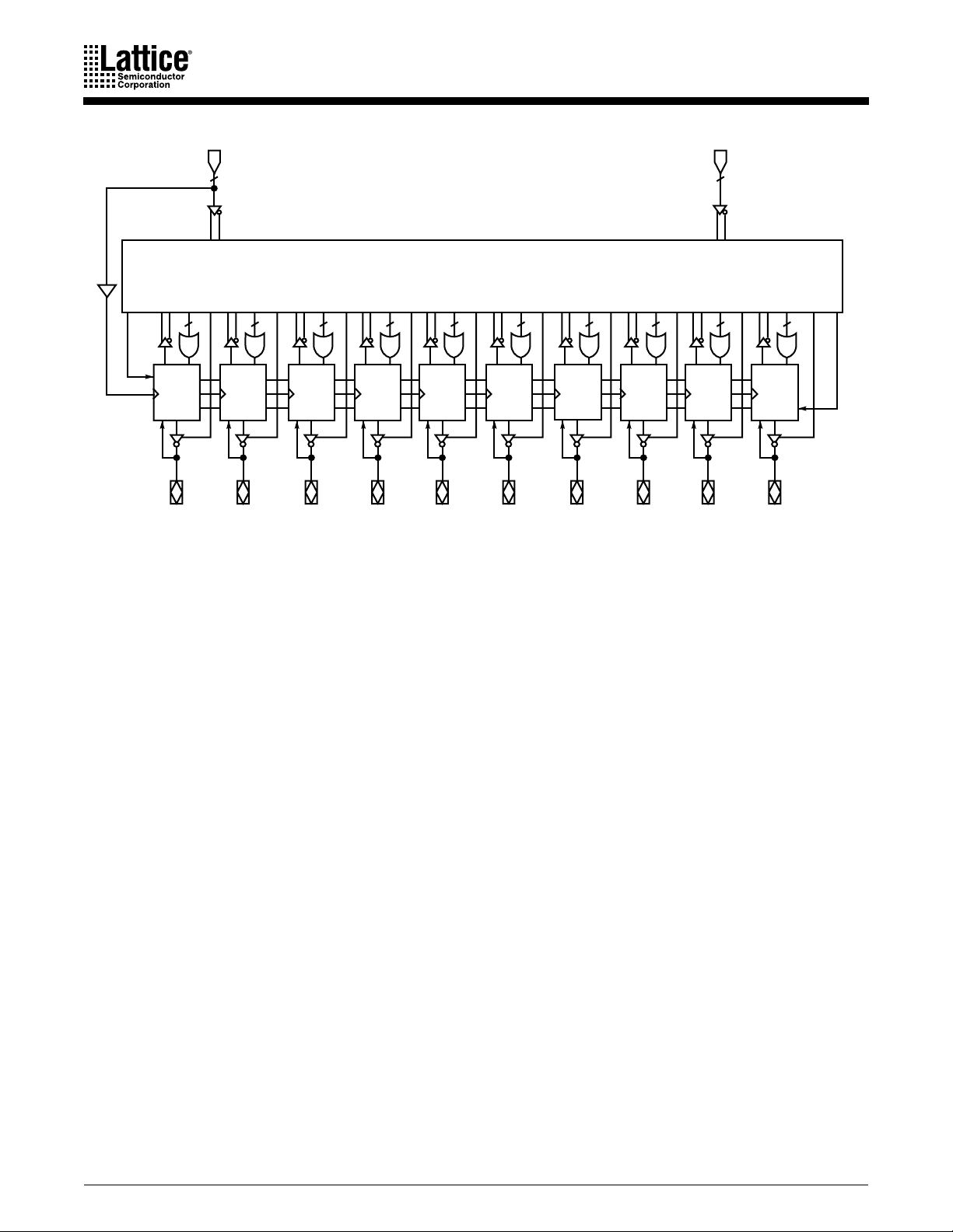
The product terms are connected to the fixed OR array with a varied distribution from 8 to 16
USE GAL DEVICES FOR
across the outputs (see Block Diagram). The OR sum of the products feeds the output macrocell.
Each macrocell can be programmed as registered or combinatorial, and active high or active low.
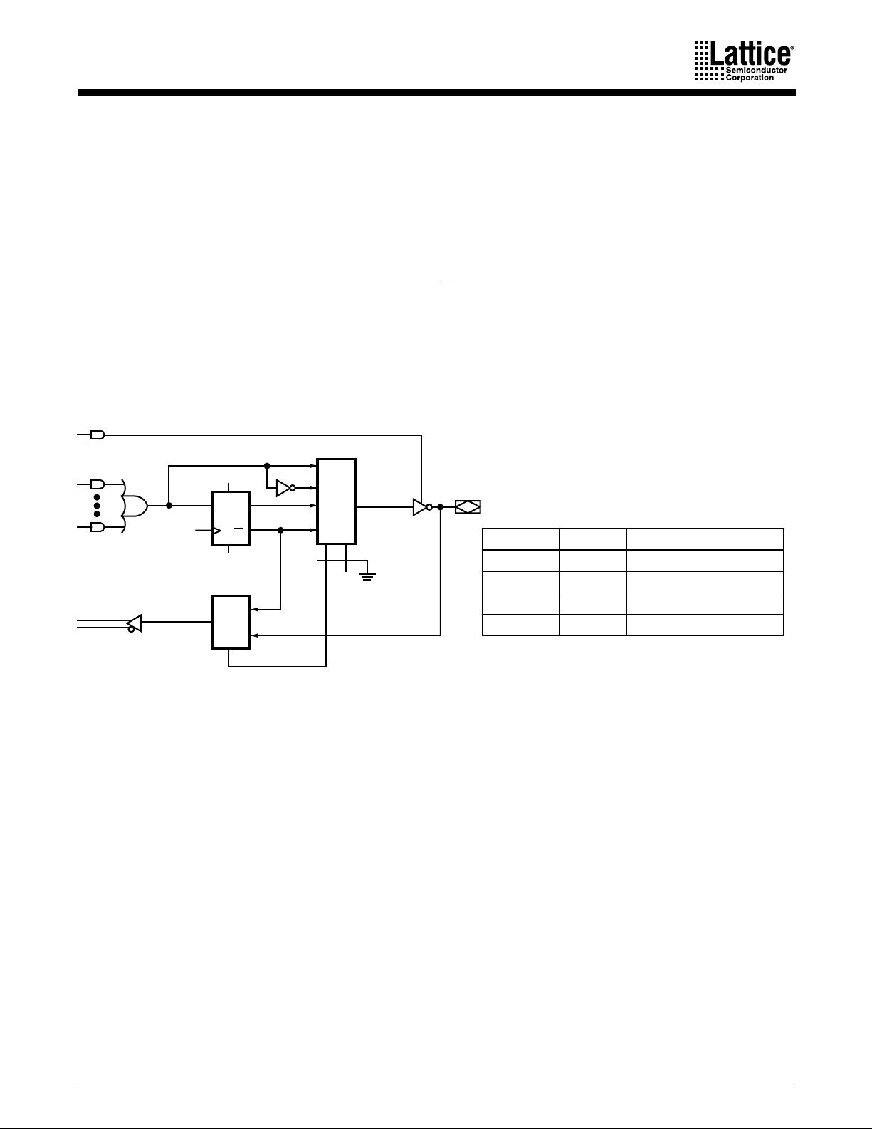
The output configuration is determined by two bits controlling two multiplexers in each macrocell.
®
device built with low-voltage, high-speed, electrically-
NEW DESIGNS
Publication#
Amendment/
18956
0
Rev:
F
Issue Date:
September 2000

BLOCK DIAGRAM
1
81012141616141210 8
CLK/I
I1 - I
0
11
PROGRAMMABLE
AND ARRAY
(44 x 132)
11
RESET
OUTPUT
LOGIC
MACRO
CELL
I/O0 I/O1 I/O2 I/O3 I/O4 I/O5 I/O6 I/O7 I/O8 I/O9
OUTPUT
LOGIC
MACRO
CELL
OUTPUT
LOGIC
MACRO
CELL
OUTPUT
LOGIC
MACRO
CELL
OUTPUT
LOGIC
MACRO
CELL
OUTPUT
LOGIC
MACRO
CELL
OUTPUT
LOGIC
MACRO
CELL
OUTPUT
LOGIC
MACRO
CELL
OUTPUT
LOGIC
MACRO
CELL
OUTPUT
LOGIC
MACRO
CELL
PRESET
18956D-001
FUNCTIONAL DESCRIPTION
The P ALL V22V10 is the low-voltage version of the PALCE22V10. It has all the architectural features
of the PALCE22V10.
The PALLV2210Z is the low-voltage, zero-power version of the PALCE22V10. It has all the
architectural features of the PALCE22V10. In addition, the PALLV22V10Z has zero standby power
and an unused product term disable feature.
The P ALLV22V10 allows the systems engineer to implement a design on-chip by programming EE
cells to configure AND and OR gates within the device, according to the desired logic function.
Complex interconnections between gates, which previously required time-consuming layout, are
USE GAL DEVICES FOR
lifted from the PC board and placed on silicon, where they can be easily modified during
prototyping or production.
NEW DESIGNS
Product terms with all connections opened assume the logical HIGH state; product terms
connected to both true and complement of any single input assume the logical LOW state.
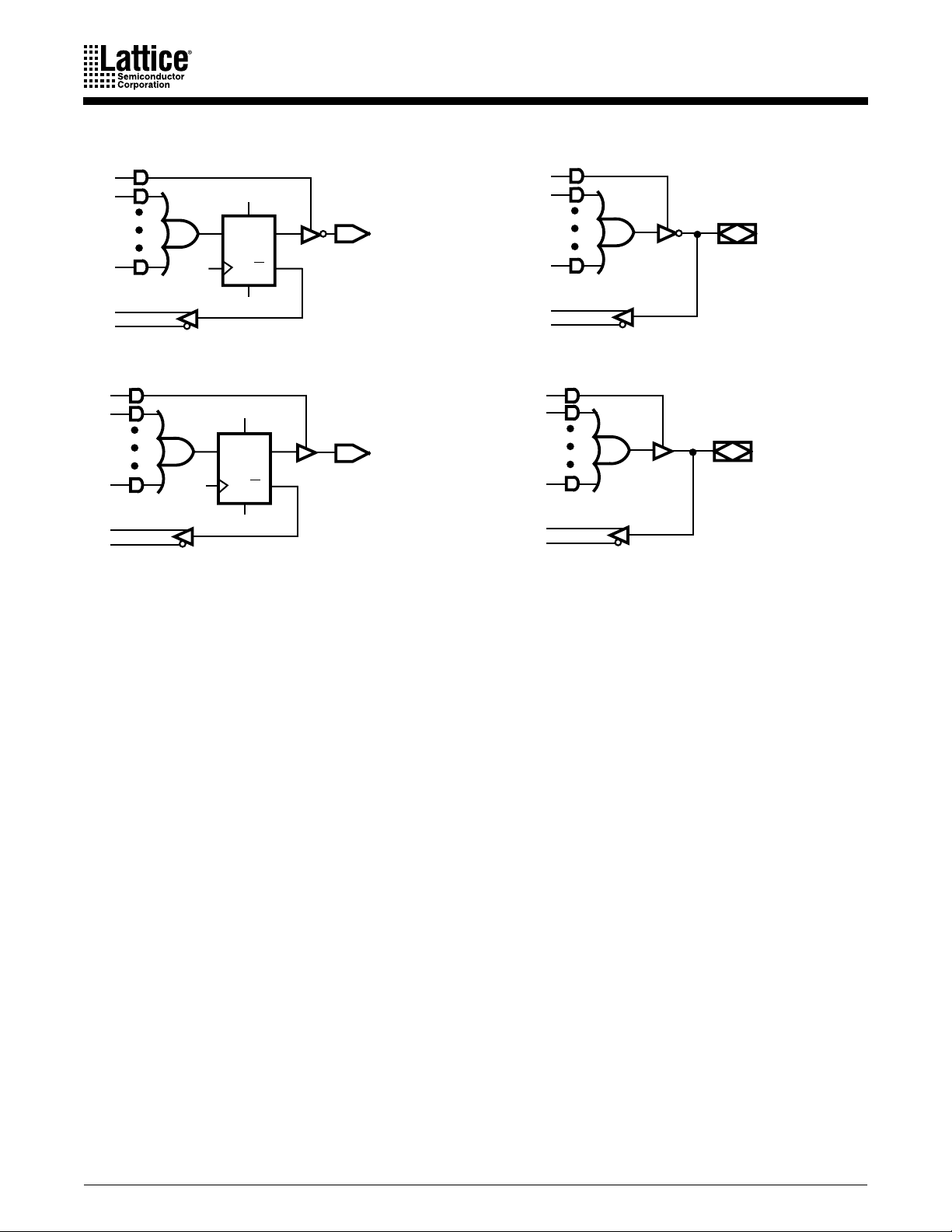
The P ALL V22V10 has 12 inputs and 10 I/O macrocells. The macrocell (Figure 1) allows one of four
potential output configurations; registered output or combinatorial I/O, active high or active low
(see Figure 2). The configuration choice is made according to the user’s design specification and
- S
corresponding programming of the configuration bits S
. Multiplexer controls are connected
0
1
to ground (0) through a programmable bit, selecting the “0” path through the multiplexer. Erasing
the bit disconnects the control line from GND and it floats to V
(1), selecting the “1” path.
CC
The device is produced with a EE cell link at each input to the AND gate array, and connections
may be selectively removed by applying appropriate voltages to the circuit. Utilizing an easilyimplemented programming algorithm, these products can be rapidly programmed to any
customized pattern.
2 PALLV22V10 and PALLV22V10Z Families

Variable Input/Output Pin Ratio
The PALLV22V10 has twelve dedicated input lines, and each macrocell output can be an I/O pin.
Buffers for device inputs have complementary outputs to provide user-programmable input signal
polarity. Unused input pins should be tied to V
or GND.
CC
Registered Output Configuration
Each macrocell of the P ALLV22V10 includes a D-type flip-flop for data storage and synchronization.
The flip-flop is loaded on the LOW-to-HIGH transition of the clock input. In the registered
configuration (S
= 0), the array feedback is from
1
Q of the flip-flop.
Combinatorial I/O Configuration
Any macrocell can be configured as combinatorial by selecting the multiplexer path that bypasses
the flip-flop (S
= 1). In the combinatorial configuration, the feedback is from the pin.
1
S
10
11
00
01
1
I/O
n
S
1
0 0 Registered/Active Low
S
0
0 1 Registered/Active High
1 0 Combinatorial/Active Low
1 1 Combinatorial/Active High
0 = Programmed EE bit
1 = Erased (charged) EE bit
S
0
Output Configuration
CLK
AR
DQ
Q
SP
0
1
NEW DESIGNS
18956C-004
USE GAL DEVICES FOR
Figure 1. Output Logic Macrocell Diagram
PALLV22V10 and PALLV22V10Z Families 3

AR
DQ
CLK
a. Registered/active low
CLK
c. Registered/active high
Q
SP
AR
DQ
Q
SP
S0 = 0
S1 = 0
b. Combinatorial/active low
S0 = 1
S1 = 0
d. Combinatorial/active high
Figure 2. Macrocell Configuration Options
S0 = 0
S1 = 1
S
= 1
0
S1 = 1
18956D-005
Programmable Three-State Outputs
Each output has a three-state output buffer with three-state control. A product term controls the
buffer, allowing enable and disable to be a function of any product of device inputs or output
feedback. The combinatorial output provides a bi-directional I/O pin, and may be configured as
a dedicated input if the buffer is always disabled.
Programmable Output Polarity
The polarity of each macrocell output can be active high or active low, either to match output
USE GAL DEVICES FOR
NEW DESIGNS
signal needs or to reduce product terms. Programmable polarity allows Boolean expressions to be
written in their most compact form (true or inverted), and the output can still be of the desired
polarity. It can also save “DeMorganizing” efforts.
Selection is controlled by programmable bit S
in the output macrocell, and affects both registered
0
and combinatorial outputs. Selection is automatic, based on the design specification and pin
definitions. If the pin definition and output equation have the same polarity, the output is
programmed to be active high (S
= 1).
0
Preset/Reset
For initialization, the PALLV22V10 has additional preset and reset product terms. These terms are
connected to all registered outputs. When the synchronous preset (SP) product term is asserted
high, the output registers will be loaded with a HIGH on the next LOW-to-HIGH clock transition.
When the asynchronous reset (AR) product term is asserted high, the output registers will be
immediately loaded with a LOW independent of the clock.
4 PALLV22V10 and PALLV22V10Z Families

Note that preset and reset control the flip-flop, not the output pin. The output level is determined
by the output polarity selected.
Benefits of Lower Operating Voltage
The PALLV22V10 has an operating voltage range of 3.0 V to 3.6 V. Low voltage allows for lower
operating power consumption, longer battery life, and/or smaller batteries for notebook
applications.
Because power is proportional to the square of the voltage, reduction of the supply voltage from
5.0 V to 3.3 V significantly reduces power consumption. This directly translates to longer battery
life for portable applications. Lower power consumption can also be used to reduce the size and
weight of the battery. Thus, 3.3 V designs facilitate a reduction in the form factor.
A lower operating voltage results in a reduction of I/O voltage swings. This reduces noise
generation and provides a less hostile environment for board design. A lower operating voltage
also reduces electromagnetic radiation noise and makes obtaining FCC approval easier.
3.3-V (CMOS) and 5-V (CMOS and TTL) Compatible Inputs and I/O
Input voltages can be at TTL levels. Additionally, the PALLV22V10 can be driven with true 5-V
CMOS levels due to special input and I/O buffer circuitry.
Power-Up Reset
All flip-flops power up to a logic LOW for predictable system initialization. Outputs of the
PALLV22V10 will depend on the programmed output polarity. The V
and the reset delay time is 1000ns maximum.
Register Preload
The registers on the PALLV22V10 can be preloaded from the output pins to facilitate functional
testing of complex state machine designs. This feature allows direct loading of arbitrary states,
making it unnecessary to cycle through long test vector sequences to reach a desired state. In
addition, transitions from illegal states can be verified by loading illegal states and observing
proper recovery.
Security Bit
After programming and verification, a PALLV22V10 design can be secured by programming the
security EE bit. Once programmed, this bit defeats readback of the internal programmed pattern
by a device programmer, securing proprietary designs from competitors. When the security bit is
programmed, the array will read as if every bit is erased, and preload will be disabled.
USE GAL DEVICES FOR
NEW DESIGNS
rise must be monotonic,
CC
The bit can only be erased in conjunction with erasure of the entire pattern.
Programming and Erasing
The PALLV22V10 can be programmed on standard logic programmers. It also may be erased to
reset a previously configured device back to its unprogrammed state. Erasure is automatically
performed by the programming hardware. No special erase operation is required.
PALLV22V10 and PALLV22V10Z Families 5

Quality and Testability
The PALLV22V10 offers a very high level of built-in quality. The erasability of the CMOS
PALLV22V10 allows direct testing of the device array to guarantee 100% programming and
functional yields.
Technology
The high-speed PALLV22V10 is fabricated with Vantis’ advanced electrically-erasable (EE) CMOS
process. The array connections are formed with proven EE cells. Inputs and outputs are designed
to be 3.3-V and 5-V device compatible. This technology provides strong input-clamp diodes,
output slew-rate control, and a grounded substrate for clean switching.
Zero-Standby Power Mode
The PALLV22V10Z features a zero-standby power mode. When none of the inputs switch for an
extended period (typically 30 ns), the PALLV22V10Z will go into standby mode, shutting down
most of its internal circuitry. The current will go to almost zero (I
maintain the states held before the device went into the standby mode.
<30 µA). The outputs will
CC
If a macrocell is used in registered mode, switching pin CLK/I
for that macrocell. If a macrocell is used in combinatorial mode, switching pin CLK/I
standby mode status for that macrocell.
This feature reduces dynamic I
macrocells are used as registers and only CLK/I
mode, but dynamic I
current. The use of combinatorial macrocells will add on average 5 mA per macrocell (at 25 MHz)
under these same conditions.
When any input switches, the internal circuitry is fully enabled, and power consumption returns
to normal. This feature results in considerable power savings for operation at low to medium
frequencies.
Product-Term Disable
On a programmed PALLV22V10Z, any product terms that are not used are disabled. Power is cut
off from these product terms so that they do not draw current. Product-term disabling results in
considerable power savings. This saving is greater at the higher frequencies.
Further hints on minimizing power consumption can be found in a separate document entitled,
Minimizing Power Consumption with Zero-Power PLDs .
will typically be <2 mA. This is because only the CLK/I
CC
USE GAL DEVICES FOR
proportionally to the number of registered macrocells used. If all
CC
is switching, the device will not be in standby
0
NEW DESIGNS
will not affect standby mode status
0
will affect
0
buffer will draw
0
6 PALLV22V10 and PALLV22V10Z Families
 Loading...