

Lattice Semiconductor Corporation PALCE22V10H-15JI-4, PALCE22V10H-15PC-4, PALCE22V10H-15PI-4, PALCE22V10H-15SC-4, PALCE22V10H-20JI-4 Datasheet
...
PALCE22V10
PALCE22V10Z
COM'L: H-5/7/10/15/25,Q-10/15/25 IND: H-10/15/20/25
COM'L: -25 IND: -15/25
PALCE22V10 and PALCE22V10Z
Families
24-Pin EE CMOS (Zero P o wer) V er satile PAL Device
DISTINCTIVE CHARACTERISTICS
◆
As fast as 5-ns propagation delay and 142.8 MHz f
Low-power EE CMOS
◆
10 macrocells programmable as registered or combinatorial, and active high or active low to
◆
match application needs
◆
Varied product term distribution allows up to 16 product terms per output for complex
functions
Peripheral Component Interconnect (PCI) compliant (-5/-7/-10)
◆
Global asynchronous reset and synchronous preset for initialization
◆
◆
Power-up reset for initialization and register preload for testability
◆
Extensive third-party software and programmer support
24-pin SKINNY DIP, 24-pin SOIC, and 28-pin PLCC
◆
◆
5-ns and 7.5-ns versions utilize split leadframes for improved performance
(external)
MAX
GENERAL DESCRIPTION
The P ALCE22V10 provides user-programmable logic for replacing conventional SSI/MSI gates and
flip-flops at a reduced chip count.
®
The PALCE22V10Z is an advanced PAL
erasable CMOS technology. It provides user-programmable logic for replacing conventional zeropower CMOS SSI/MSI gates and flip-flops at a reduced chip count.
The PALCE22V10Z provides zero standby power and high speed. At 30 µA maximum standby
current, the PALCE22V10Z allows battery-powered operation for an extended period.
The P AL device implements the familiar Boolean logic transfer function, the sum of products. The
P AL device is a programmable AND array driving a fixed OR array. The AND array is programmed
to create custom product terms, while the OR array sums selected terms at the outputs.
The product terms are connected to the fixed OR array with a varied distribution from 8 to16 across
the outputs (see Block Diagram). The OR sum of the products feeds the output macrocell. Each
macrocell can be programmed as registered or combinatorial, and active-high or active low. The
output configuration is determined by two bits controlling two multiplexers in each macrocell.
device built with zero-power, high-speed, electrically-
Publication#
Amendment/
16564
0
Rev:
E
Issue Date:
November 1998
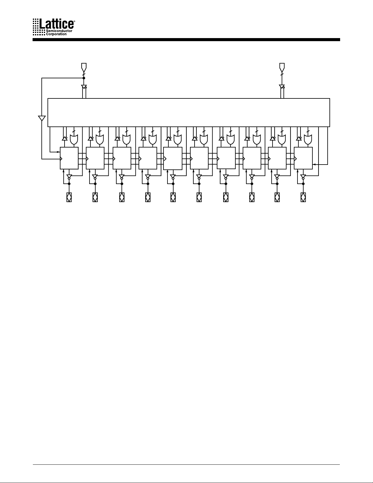
BLOCK DIAGRAM
I1 - I
11
11
OUTPUT
LOGIC
MACRO
CELL
PRESET
RESET
CLK/I
0
1
PROGRAMMABLE
AND ARRAY
(44 x 132)
81012141616141210 8
OUTPUT
LOGIC
MACRO
CELL
I/O0 I/O1 I/O2 I/O3 I/O4 I/O5 I/O6 I/O7 I/O8 I/O9
OUTPUT
LOGIC
MACRO
CELL
OUTPUT
LOGIC
MACRO
CELL
OUTPUT
LOGIC
MACRO
CELL
OUTPUT
LOGIC
MACRO
CELL
OUTPUT
LOGIC
MACRO
CELL
OUTPUT
LOGIC
MACRO
CELL
OUTPUT
LOGIC
MACRO
CELL
OUTPUT
LOGIC
MACRO
CELL
FUNCTIONAL DESCRIPTION
The PALCE22V10 allows the systems engineer to implement the design on-chip, by programming
EE cells to configure AND and OR gates within the device, according to the desired logic function.
Complex interconnections between gates, which previously required time-consuming layout, are
lifted from the PC board and placed on silicon, where they can be easily modified during
prototyping or production.
The P ALCE22V10Z is the zero-power version of the P ALCE22V10. It has all the architectural features
of the PALCE22V10. In addition, the PALCE22V10Z has zero standby power and unused product
term disable.
Product terms with all connections opened assume the logical HIGH state; product terms
connected to both true and complement of any single input assume the logical LOW state.
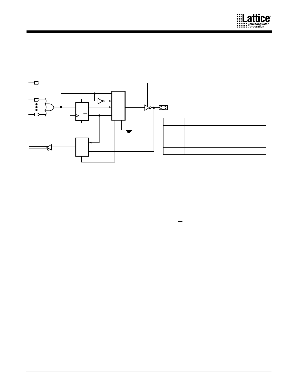
The P ALCE22V10 has 12 inputs and 10 I/O macrocells. The macrocell (Figure 1) allows one of four
potential output configurations registered output or combinatorial I/O, active high or active low
(see Figure 1). The configuration choice is made according to the user’s design specification and
- S
corresponding programming of the configuration bits S
. Multiplexer controls are connected
0
1
to ground (0) through a programmable bit, selecting the “0” path through the multiplexer. Erasing
the bit disconnects the control line from GND and it is driven to a high level, selecting the “1” path.
The device is produced with an EE cell link at each input to the AND gate array, and connections
may be selectively removed by applying appropriate voltages to the circuit. Utilizing an easilyimplemented programming algorithm, these products can be rapidly programmed to any
customized pattern.
2 PALCE22V10 and PALCE22V10Z Families
Variable Input/Output Pin Ratio
The PALCE22V10 has twelve dedicated input lines, and each macrocell output can be an I/O pin.
Buffers for device inputs have complementary outputs to provide user-programmable input signal
polarity. Unused input pins should be tied to V
or GND.
CC
10
11
00
01
S
1
S
0
Figure 1. Output Logic Macrocell Diagram
I/O
n
S
1
0 0 Registered/Active Low
0 1 Registered/Active High
1 0 Combinatorial/Active Low
1 1 Combinatorial/Active High
0 = Programmed EE bit
1 = Erased (charged) EE bit
S
0
Output Configuration
16564E-004
CLK
AR
D Q
Q
SP
0
1
Registered Output Configuration
Each macrocell of the PALCE22V10 includes a D-type flip-flop for data storage and
synchronization. The flip-flop is loaded on the LOW-to-HIGH transition of the clock input. In the
registered configuration (S
Combinatorial I/O Configuration
= 0), the array feedback is from Q of the flip-flop.
1
Any macrocell can be configured as combinatorial by selecting the multiplexer path that bypasses
the flip-flop (S
= 1). In the combinatorial configuration, the feedback is from the pin.
1
PALCE22V10 and PALCE22V10Z Families 3
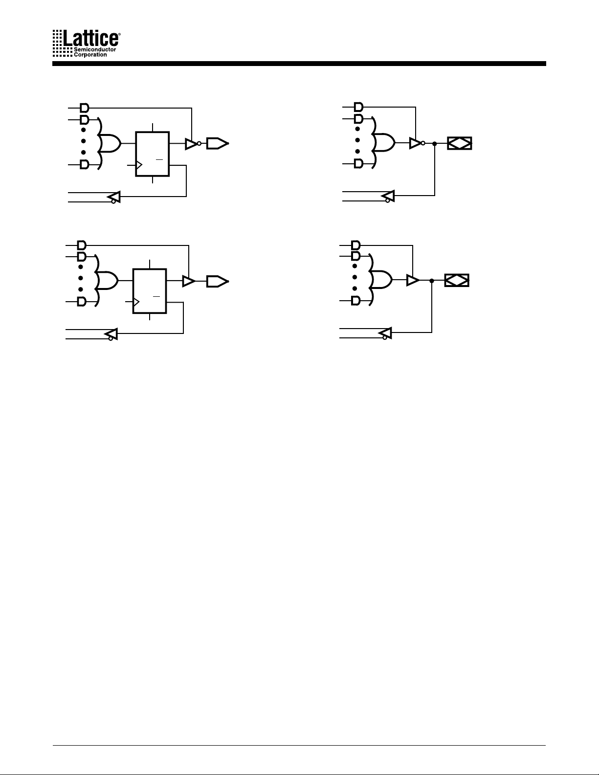
AR
DQ
CLK
a. Registered/active low
CLK
c. Registered/active high
Q
SP
AR
DQ
Q
SP
S0 = 0
S1 = 0
b. Combinatorial/active low
S0 = 1
S1 = 0
d. Combinatorial/active high
Figure 2. Macrocell Configuration Options
S0 = 0
S1 = 1
S
= 1
0
S1 = 1
16564E-005
Programmable Three-State Outputs
Each output has a three-state output buffer with three-state control. A product term controls the
buffer, allowing enable and disable to be a function of any product of device inputs or output
feedback. The combinatorial output provides a bi-directional I/O pin, and may be configured as
a dedicated input if the buffer is always disabled.
Programmable Output Polarity
The polarity of each macrocell output can be active high or active low, either to match output
signal needs or to reduce product terms. Programmable polarity allows Boolean expressions to be
written in their most compact form (true or inverted), and the output can still be of the desired
polarity. It can also save “DeMorganizing” efforts.
Selection is controlled by programmable bit S
in the output macrocell, and affects both registered
0
and combinatorial outputs. Selection is automatic, based on the design specification and pin
definitions. If the pin definition and output equation have the same polarity, the output is
programmed to be active high (S
= 1).
0
Preset/Reset
For initialization, the PALCE22V10 has preset and reset product terms. These terms are connected
to all registered outputs. When the synchronous preset (SP) product term is asserted high, the
output registers will be loaded with a HIGH on the next LOW-to-HIGH clock transition. When the
asynchronous reset (AR) product term is asserted high, the output registers will be immediately
loaded with a LOW independent of the clock.
4 PALCE22V10 and PALCE22V10Z Families

Note that preset and reset control the flip-flop, not the output pin. The output level is determined
by the output polarity selected.
Power-Up Reset
All flip-flops power up to a logic LOW for predictable system initialization. Outputs of the
PALCE22V10 will depend on the programmed output polarity. The V
rise must be monotonic,
CC
and the reset delay time is 1000ns maximum.
Register Preload
The register on the PALCE22V10 can be preloaded from the output pins to facilitate functional
testing of complex state machine designs. This feature allows direct loading of arbitrary states,
making it unnecessary to cycle through long test vector sequences to reach a desired state. In
addition, transitions from illegal states can be verified by loading illegal states and observing
proper recovery.
Security Bit
After programming and verification, a PALCE22V10 design can be secured by programming the
security EE bit. Once programmed, this bit defeats readback of the internal programmed pattern
by a device programmer, securing proprietary designs from competitors. When the security bit is
programmed, the array will read as if every bit is erased, and preload will be disabled.
The bit can only be erased in conjunction with erasure of the entire pattern.
Programming and Erasing
The PALCE22V10 can be programmed on standard logic programmers. It also may be erased to
reset a previously configured device back to its unprogrammed state. Erasure is automatically
performed by the programming hardware. No special erase operation is required.
Quality and Testability
The P ALCE22V10 offers a very high level of built-in quality. The erasability of the device provides
a direct means of verifying performance of all AC and DC parameters. In addition, this verifies
complete programmability and functionality of the device to provide the highest programming
yields and post-programming functional yields in the industry.
Technology
The high-speed PALCE22V10 is fabricated with Vantis’ advanced electrically erasable (EE) CMOS
process. The array connections are formed with proven EE cells. Inputs and outputs are designed
to be compatible with TTL devices. This technology provides strong input clamp diodes, output
slew-rate control, and a grounded substrate for clean switching.
PCI Compliance
The PALCE22V10H devices in the -5/-7/-10 speed grades are fully compliant with the PCI Local
Bus Specification
published by the PCI Special Interest Group. The PALCE22V10H’s predictable
timing ensures compliance with the PCI AC specifications independent of the design.
Zero-Standby Power Mode
The PALCE22V10Z features a zero-standby power mode. When none of the inputs switch for an
extended period (typically 50 ns), the PALCE22V10Z will go into standby mode, shutting down
PALCE22V10 and PALCE22V10Z Families 5

most of its internal circuitry. The current will go to almost zero (I
< 30 µA). The outputs will
CC
maintain the states held before the device went into the standby mode.
When any input switches, the internal circuitry is fully enabled, and power consumption returns
to normal. This feature results in considerable power savings for operation at low to medium
frequencies. This saving is illustrated in the I
vs. frequency graph.
CC
Product-Term Disable
On a programmed PALCE22V10Z, any product terms that are not used are disabled. Power is cut
off from these product terms so that they do not draw current. As shown in the I
vs. frequency
CC
graph, product-term disabling results in considerable power savings. This saving is greater at the
higher frequencies.
Further hints on minimizing power consumption can be found in a separate document entitled,
Minimizing Power Consumption with Zero-Power PLDs .
6 PALCE22V10 and PALCE22V10Z Families
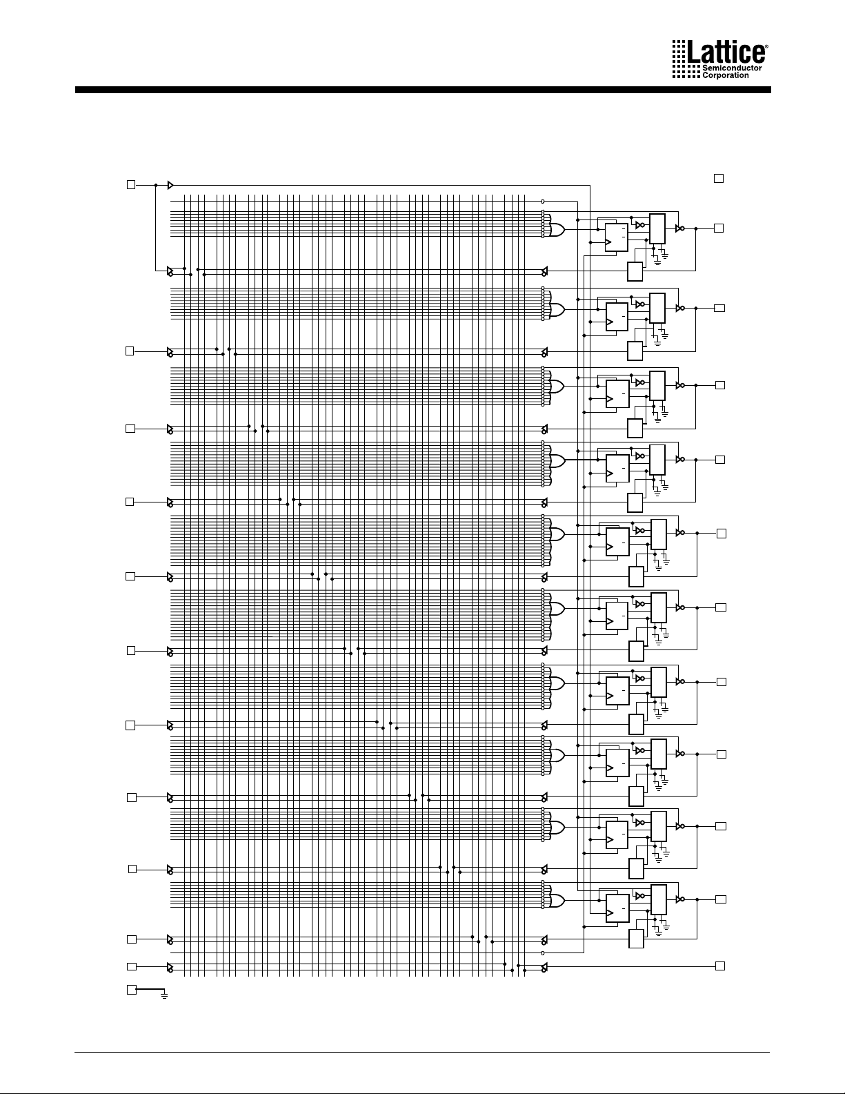
LOGIC DIAGRAM
CLK/I01
I
1
I
2
I
3
I
4
I
5
I
6
I
7
I
8
I
9
I
10
GND
(3)
(4)
(5)
(6)
(7)
(9)
(10)
(11)
10
(12)
(13)
12
(14)
24
(2)
2
3
4
5
6
7
8
9
0 34 78 1112151619202324272831323536394043
0
1
9
10
20
21
33
34
48
49
65
66
82
83
97
98
110
111
121
122
130
131
AR
10
1
1
AR
D
Q
00
1
Q
0
SP
0
1
10
1
1
AR
D
Q
00
1
Q
0
SP
0
1
10
1
1
AR
D
Q
00
1
Q
0
SP
0
1
10
1
1
AR
D
Q
00
1
Q
0
SP
0
1
10
1
1
AR
D
Q
00
1
0
Q
SP
0
1
10
1
1
AR
D
Q
00
1
0
Q
SP
0
1
10
1
1
AR
D
Q
00
1
0
Q
SP
0
1
10
1
1
AR
D
Q
00
1
0
Q
SP
0
1
10
1
1
AR
D
Q
00
1
Q
0
SP
0
1
10
1
1
AR
D
Q
00
1
0
Q
SP
0
SP
1
11
0 34 78 1112151619202324272831323536394043
(28)VCC
(27)
(26)
(25)
(24)
(23)
18
(21)
17
(20)
16
(19)
15
(18)
14
(17)
(16)
I/O923
I/O22
8
I/O21
7
I/O20
6
I/O19
5
I/O
4
I/O
3
I/O
2
I/O
1
I/O
0
I13
11
16564E-006
PALCE22V10 and PALCE22V10Z Families 7
µ
µ
µ
ABSOLUTE MAXIMUM RATINGS
Storage Temperature. . . . . . . . . . . . . .-65 ° C to +150 ° C
Ambient Temperature with
Power Applied . . . . . . . . . . . . . . . . . .-55 ° C to +125 ° C
Supply Voltage with
Respect to Ground . . . . . . . . . . . . . . .-0.5 V to +7.0 V
DC Input Voltage . . . . . . . . . . . .-0.5 V to V
DC Output or I/O Pin Voltage . . .-0.5 V to V
+ 1.0 V
CC
+ 1.0 V
CC
OPERATING RANGES
Commercial (C) Devices
Ambient Temperature (T
Operating in Free Air. . . . . . . . . . . . . . . 0 ° C to +75 ° C
Supply Voltage (V
CC
Respect to Ground. . . . . . . . . . . . . +4.75 V to +5.25 V
Operating ranges define those limits between which the functionality of the device is guaranteed.
A
) with
)
Static Discharge Voltage . . . . . . . . . . . . . . . . . 2001 V
Latchup Current (T
Stresses above those listed under Absolute Maximum Ratings
may cause permanent device failure. Functionality at or above
these limits is not implied. Exposure to Absolute Maximum
Ratings for extended periods may affect device reliability.
Programming conditions may vary.
= 0 ° C to +75 ° C) . . . . . . . .100 mA
A
DC CHARACTERISTICS OVER COMMERCIAL OPERATING RANGES
Parameter
Symbol Parameter Description Test Conditions Min Max Unit
V
OH
V
OL
V
IH
V
IL
I
IH
I
IL
I
OZH
I
OZL
I
SC
(Static) Supply Current Outputs Open, (I
I
CC
(Dynamic) Supply Current Outputs Open, (I
I
CC
Output HIGH Voltage I
Output LOW Voltage I
Input HIGH Voltage
Input LOW Voltage
Input HIGH Leakage Current V
Input LOW Leakage Current VIN = 0 V, VCC = Max (Note 2) -100
Off-State Output Leakage
Current HIGH
Off-State Output Leakage
Current LOW
Output Short-Circuit
Current
= -3.2 mA, VIN = V
OH
= 16 mA, V
OL
Guaranteed Input Logical HIGH
Voltage for all Inputs (Note 1)
Guaranteed Input Logical LOW
Voltage for all Inputs (Note 1)
= VCC, VCC = Max (Note 2) 10
IN
= VCC, VCC = Max,
V
OUT
V
= V
IN
IL
= 0 V, V
V
OUT
V
= VIL or VIH (Note 2)
IN
V
= 0.5 V, V
OUT
or V
IH
= V
or V
IN
IH
or VIH (Note 2)
= Max,
CC
= Max (Note 3) -30 -130 mA
CC
= 0 mA), VCC = Max 125 mA
OUT
= 0 mA), V
OUT
= Min 2.4 V
IL, VCC
= Min 0.4 V
IL, VCC
2.0 V
0.8 V
10
-100
= Max, f = 25 MHz 140 mA
CC
A
A
µ
A
A
Notes:
1. These are absolute values with respect to the device ground, and all overshoots due to system and tester noise are included.
2. I/O pin leakage is the worst case of I
3. Not more than one output should be tested at a time, and the duration of the short-circuit test should not exceed one second.
= 0.5 V has been chosen to avoid test problems caused by tester ground degradation.
V
OUT
and I
IL
(or IIH and I
OZL
OZH
).
8 PALCE22V10H-5 (Com’l)
CAPACITANCE
1
Parameter
Symbol Parameter Description Test Conditions Typ Unit
C
IN
C
OUT
Input Capacitance V
Output Capacitance V
= 2.0 V VCC = 5.0 V
IN
= 2.0 V 8
OUT
T
= 25
A
f = 1 MHz
°C
5
pF
Note:
1. These parameters are not 100% tested, but are evaluated at initial characterization and at any time the design is modified where
capacitance may be affected.
SWITCHING CHARACTERISTICS OVER COMMERCIAL OPERATING RANGES
Parameter
Symbol Parameter Description
t
PD
t
S1
t
S2
t
H
t
CO
t
SKEWR
t
AR
t
ARW
t
ARR
t
SPR
t
WL
t
WH
Input or Feedback to Combinatorial Output 5 ns
Setup Time from Input or Feedback 3 ns
Setup Time from SP to Clock 4 ns
Hold Time 0 ns
Clock to Output 4ns
Skew Between Registered Outputs (Note 2) 0.5 ns
Asynchronous Reset to Registered Output 7.5 ns
Asynchronous Reset Width 4.5 ns
Asynchronous Reset Recovery Time 4.5 ns
Synchronous Preset Recovery Time 4.5 ns
Clock Width
LOW 2.5 ns
HIGH 2.5 ns
External Feedback 1/(t
f
MAX
Maximum Frequency (Note 3)
Internal Feedback (f
No Feedback 1/(t
t
EA
t
ER
Input to Output Enable Using Product Term Control 6 ns
Input to Output Disable Using Product Term Control 5.5 ns
+ tCO) 142.8 MHz
S
) 1/(tS + tCF) (Note 4) 150 MHz
CNT
+ tWL) 200 MHz
WH
-5
1
UnitMin Max
Notes:
1. See “Switching Test Circuit” for test conditions.
2. Skew is measured with all outputs switching in the same direction.
3. These parameters are not 100% tested, but are calculated at initial characterization and at any time the design is modified where
frequency may be affected.
is a calculated value and is not guaranteed. t
4. t
CF
t
CF
= 1/f
(internal feedback) - tS.
MAX
can be found using the following equation:
CF
PALCE22V10H-5 (Com’l) 9
ABSOLUTE MAXIMUM RATINGS
OPERATING RANGES
Storage Temperature. . . . . . . . . . . . . .-65°C to +150°C
Ambient Temperature with
Power Applied . . . . . . . . . . . . . . . . . .-55°C to +125°C
Supply Voltage with Respect
to Ground . . . . . . . . . . . . . . . . . . . . .-0.5 V to +7.0 V
DC Input Voltage . . . . . . . . . . . .-0.5 V to VCC + 1.0 V
DC Output or I/O Pin Voltage . . .-0.5 V to VCC + 1.0 V
Commercial (C) Devices
Ambient Temperature (TA)
Operating in Free Air. . . . . . . . . . . . . . . 0°C to +75°C
Supply Voltage (VCC) with
Respect to Ground. . . . . . . . . . . . . +4.75 V to +5.25 V
Operating ranges define those limits between which the functionality of the device is guaranteed.
Static Discharge Voltage . . . . . . . . . . . . . . . . . 2001 V
Latchup Current (TA = 0°C to +75°C) . . . . . . . .100 mA
Stresses above those listed under Absolute Maximum Ratings
may cause permanent device failure. Functionality at or above
these limits is not implied. Exposure to Absolute Maximum
Ratings for extended periods may affect device reliability.
Programming conditions may vary.
DC CHARACTERISTICS OVER COMMERCIAL OPERATING RANGES
Symbol Parameter Description Test Conditions Min Max Unit
V
OH
V
OL
V
IH
V
IL
I
IH
I
IL
I
OZH
I
OZL
I
SC
(Static) Supply Current Outputs Open, (I
I
CC
(Dynamic) Supply Current Outputs Open, (I
I
CC
Output HIGH Voltage IOH = -3.2 mA, VIN = V
Output LOW Voltage I
Input HIGH Voltage
Input LOW Voltage
Input HIGH Leakage Current VIN = VCC, VCC = Max (Note 2) 10 µA
Input LOW Leakage Current VIN = 0 V, VCC = Max (Note 2) -100 µA
Off-State Output Leakage
Current HIGH
Off-State Output Leakage
Current LOW
Output Short-Circuit
Current
= 16 mA, VIN = V
OL
Guaranteed Input Logical HIGH
Voltage for all Inputs (Note 1)
Guaranteed Input Logical LOW
Voltage for all Inputs (Note 1)
V
= VCC, VCC = Max, V
OUT
V
= 0 V, V
OUT
V
= 0.5 V, VCC = Max
OUT
T
= 25°C (Note 3)
A
= Max, V
CC
OUT
OUT
or V
IH
or V
IH
IN
IN
= 0 mA), VCC = Max 115 mA
= 0 mA), VCC = Max, f = 25 MHz 140 mA
= Min 2.4 V
IL, VCC
= Min 0.4 V
IL, VCC
2.0 V
0.8 V
= V
or VIH (Note 2) 10 µA
IL
= VIL or VIH (Note 2) -100 µA
-30 -130 mA
Notes:
1. These are absolute values with respect to the device ground, and all overshoots due to system and tester noise are included.
2. I/O pin leakage is the worst case of I
3. Not more than one output should be tested at a time. Duration of the short-circuit test should not exceed one second.
= 0.5 V has been chosen to avoid test problems caused by tester ground degradation.
V
OUT
and I
IL
(or IIH and I
OZL
OZH
).
10 PALCE22V10H-7 (Com’l)
CAPACITANCE
1
Parameter
Symbol Parameter Description Test Conditions Typ Unit
C
IN
C
OUT
Input Capacitance VIN = 2.0 V VCC = 5.0 V
T
= 25°C
Output Capacitance V
= 2.0 V 8
OUT
A
f = 1 MHz
5
pF
Note:
1. These parameters are not 100% tested, but are evaluated at initial characterization and at any time the design is modified where
capacitance may be affected.
SWITCHING CHARACTERISTICS OVER COMMERCIAL OPERATING RANGES
-7
Parameter
Symbol Parameter Description
t
PD
t
S1
t
S2
t
H
t
CO
t
SKEWR
t
AR
t
ARW
t
ARR
t
SPR
t
WL
t
WH
Input or Feedback to Combinatorial Output 3 7.5 3 7.5 ns
Setup Time from Input or Feedback 5 4.5 ns
Setup Time from SP to Clock 6 6 ns
Hold Time 0 0 ns
Clock to Output 2 5 2 4.5 ns
Skew Between Registered Outputs (Note 2) 1 1 ns
Asynchronous Reset to Registered Output 10 10 ns
Asynchronous Reset Width 7 7 ns
Asynchronous Reset Recovery Time 7 7 ns
Synchronous Preset Recovery Time 7 7 ns
Clock Width
LOW 3.5 3.0 ns
HIGH 3.5 3.0 ns
External Feedback 1/(t
f
MAX
Maximum Frequency
(Note 3)
Internal Feedback
(f
)
CNT
No Feedback 1/(t
t
EA
t
ER
Input to Output Enable Using Product Term Control 7.5 7.5 ns
Input to Output Disable Using Product Term Control 7.5 7.5 ns
+ tCO) 100 111 MHz
S
+ tCF) (Note 4) 125 133 MHz
1/(t
S
+ tWL) 142.8 166 MHz
WH
PDIP PLCC
Min Max Min Max
1
Unit
Notes:
1. See “Switching Test Circuit” for test conditions.
2. Skew is measured with all outputs switching in the same direction.
3. These parameters are not 100% tested, but are calculated at initial characterization and at any time the design is modified where
frequency may be affected.
is a calculated value and is not guaranteed. tCF can be found using the following equation:
4. t
CF
t
CF
= 1/f
(internal feedback) - tS.
MAX
PALCE22V10H-7 (Com’l) 11

ABSOLUTE MAXIMUM RATINGS
OPERATING RANGES
Storage Temperature. . . . . . . . . . . . . .-65°C to +150°C
Ambient Temperature with
Power Applied . . . . . . . . . . . . . . . . . .-55°C to +125°C
Supply Voltage with Respect
to Ground . . . . . . . . . . . . . . . . . . . . .-0.5 V to +7.0 V
DC Input Voltage . . . . . . . . . . . .-0.5 V to VCC + 1.0 V
DC Output or I/O Pin Voltage . . .-0.5 V to VCC + 1.0 V
Commercial (C) Devices
Ambient Temperature (TA)
Operating in Free Air. . . . . . . . . . . . . . . 0°C to +75°C
Supply Voltage (VCC) with
Respect to Ground. . . . . . . . . . . . . +4.75 V to +5.25 V
Operating ranges define those limits between which the functionality of the device is guaranteed.
Static Discharge Voltage . . . . . . . . . . . . . . . . . 2001 V
Latchup Current (TA = 0°C to +75°C) . . . . . . . .100 mA
Stresses above those listed under Absolute Maximum Ratings
may cause permanent device failure. Functionality at or above
these limits is not implied. Exposure to absolute maximum ratings for extended periods may affect device reliability.
Programming conditions may vary.
DC CHARACTERISTICS OVER COMMERCIAL OPERATING RANGES
Parameter
Symbol Parameter Description Test Conditions Min Max Unit
V
OH
V
OL
V
IH
V
IL
I
IH
I
IL
I
OZH
I
OZL
I
SC
(Dynamic) Supply Current Outputs Open , (I
I
CC
Output HIGH Voltage IOH = -3.2 mA, VIN = V
Output LOW Voltage I
Input HIGH Voltage Guaranteed Input Logical HIGH Voltage for all Inputs (Note 1) 2.0 V
Input LOW Voltage
Input HIGH Leakage Current VIN = VCC, VCC = Max (Note 2) 10 µA
Input LOW Leakage Current VIN = 0 V, VCC = Max (Note 2) -100 µA
Off-State Output Leakage
Current HIGH
Off-State Output Leakage
Current LOW
Output Short-Circuit
Current
= 16 mA, VIN = V
OL
Guaranteed Input Logical LOW
Voltage for all Inputs (Note 1)
V
= VCC, VCC = Max, V
OUT
V
= 0 V, V
OUT
V
= VIL or VIH (Note 2)
IN
V
= 0.5 V, VCC = Max
OUT
T
= 25°C (Note 3)
A
CC
= Max
or V
IH
or V
IH
IN
= 0 mA), VCC = Max, f = 25 MHz 120 mA
OUT
= Min 2.4 V
IL, VCC
= Min 0.4 V
IL, VCC
0.8 V
= V
or VIH (Note 2) 10 µA
IL
-100 µA
-30 -130 mA
Notes:
1. These are absolute values with respect to the device ground, and all overshoots due to system and tester noise are included.
2. I/O pin leakage is the worst case of I
3. Not more than one output should be tested at a time. Duration of the short-circuit test should not exceed one second.
= 0.5 V has been chosen to avoid test problems caused by tester ground degradation.
V
OUT
and I
IL
(or IIH and I
OZL
OZH
).
12 PALCE22V10H-10 (Com’l)

CAPACITANCE
1
Parameter
Symbol Parameter Description Test Conditions Typ Unit
C
IN
C
OUT
Input Capacitance VIN = 2.0 V VCC = 5.0 V
T
= 25°C
Output Capacitance V
= 2.0 V 8
OUT
A
f = 1 MHz
5
pF
Note:
1. These parameters are not 100% tested, but are evaluated at initial characterization and at any time the design is modified where
capacitance may be affected.
SWITCHING CHARACTERISTICS OVER COMMERCIAL OPERATING RANGES
Parameter
Symbol Parameter Description
t
t
t
t
t
t
t
t
t
t
t
f
t
t
PD
S1
S2
H
CO
AR
ARW
ARR
SPR
WL
WH
MAX
EA
ER
Input or Feedback to Combinatorial Output 10 ns
Setup Time from Input or Feedback 6 ns
Setup Time from SP to Clock 7 ns
Hold Time 0 ns
Clock to Output 6ns
Asynchronous Reset to Registered Output 13 ns
Asynchronous Reset Width 8 ns
Asynchronous Reset Recovery Time 8 ns
Synchronous Preset Recovery Time 8 ns
Clock Width
Maximum
Frequency
(Note 2)
LOW 4 ns
HIGH 4 ns
External Feedback 1/(t
Internal Feedback (f
No Feedback 1/(t
Input to Output Enable Using Product Term Control 10 ns
Input to Output Disable Using Product Term Control 9 ns
+ tCO) 83.3 MHz
S
) 1/(tS + tCF) (Note 3) 110 MHz
CNT
+ tWL) 125 MHz
WH
-10
UnitMin Max
1
Notes:
1. See “Switching Test Circuit” for test conditions.
2. These parameters are not 100% tested, but are calculated at initial characterization and at any time the design is modified where
frequency may be affected.
3. t
is a calculated value and is not guaranteed. tCF can be found using the following equation:
CF
t
CF
= 1/f
(internal feedback) - tS.
MAX
PALCE22V10H-10 (Com’l) 13

ABSOLUTE MAXIMUM RATINGS
OPERATING RANGES
Storage Temperature. . . . . . . . . . . . . .-65°C to +150°C
Ambient Temperature with
Power Applied . . . . . . . . . . . . . . . . . .-55°C to +125°C
Supply Voltage with Respect
to Ground . . . . . . . . . . . . . . . . . . . . .-0.5 V to +7.0 V
DC Input Voltage . . . . . . . . . . . .-0.5 V to VCC + 1.0 V
DC Output or I/O Pin
Commercial (C) Devices
Ambient Temperature (TA)
Operating in Free Air. . . . . . . . . . . . . . . 0°C to +75°C
Supply Voltage (VCC) with
Respect to Ground. . . . . . . . . . . . . +4.75 V to +5.25 V
Operating ranges define those limits between which the functionality of the device is guaranteed.
Voltage . . . . . . . . . . . . . . . . . . .-0.5 V to VCC + 1.0 V
Static Discharge Voltage . . . . . . . . . . . . . . . . . 2001 V
Latchup Current (T
Stresses above those listed under Absolute Maximum Ratings
may cause permanent device failure. Functionality at or above
these limits is not implied. Exposure to Absolute Maximum
Ratings for extended periods may affect device reliability.
Programming conditions may vary.
= 0°C to +75°C) . . . . . . . .100 mA
A
DC CHARACTERISTICS OVER COMMERCIAL OPERATING RANGES
Parameter
Symbol Parameter Description Test Conditions Min Max Unit
V
OH
V
OL
V
IH
V
IL
I
IH
I
IL
I
OZH
I
OZL
I
SC
(Static) Supply Current
I
CC
Output HIGH Voltage IOH = -3.2 mA, VIN = V
Output LOW Voltage I
Input HIGH Voltage
Input LOW Voltage
Input HIGH Leakage Current VIN = VCC, VCC = Max (Note 2) 10 µA
Input LOW Leakage Current VIN = 0 V, VCC = Max (Note 2) -100 µA
Off-State Output Leakage
Current HIGH
Off-State Output Leakage
Current LOW
Output Short-Circuit
Current
= 16 mA, VIN = V
OL
Guaranteed Input Logical HIGH
Voltage for all Inputs (Note 1)
Guaranteed Input Logical LOW
Voltage for all Inputs (Note 1)
= VCC, VCC = Max
V
OUT
= V
or VIH (Note 2)
V
IN
IL
V
= 0 V, V
OUT
V
= VIL or VIH (Note 2)
IN
V
= 0.5 V, V
OUT
T
= 25°C (Note 3)
A
= 0 V, Outputs Open (I
V
IN
V
= Max (Note 4)
CC
CC
CC
= Max
IH
= 5 V
IH
or V
or V
OUT
= Min 2.4 V
IL, VCC
= Min 0.4 V
IL, VCC
2.0 V
-100 µA
-30 -130 mA
= 0mA),
0.8 V
10 µA
55 mA
Notes:
1. These are absolute values with respect to the device ground, and all overshoots due to system and tester noise are included.
2. I/O pin leakage is the worst case of I
3. Not more than one output should be tested at a time, and the duration of the short-circuit test should not exceed one second.
= 0.5 V has been chosen to avoid test problems caused by tester ground degradation.
V
OUT
4. This parameter is guaranteed worst case under test condition. Refer to the I
characteristics.
and I
IL
(or IIH and I
OZL
OZH
).
vs. frequency graph for typical I
CC
CC
14 PALCE22V10Q-10 (Com’l)
CAPACITANCE
1
Parameter
Symbol Parameter Description Test Conditions Typ Unit
C
IN
C
OUT
Input Capacitance VIN = 2.0 V VCC = 5.0 V
T
= 25°C
Output Capacitance V
= 2.0 V 8
OUT
A
f = 1 MHz
5
pF
Note:
1. These parameters are not 100% tested, but are evaluated at initial characterization and at any time the design is modified where
capacitance may be affected.
SWITCHING CHARACTERISTICS OVER COMMERCIAL OPERATING RANGES
Parameter
Symbol Parameter Description
t
t
t
t
t
t
t
t
t
t
PD
S
H
CO
AR
ARW
ARR
SPR
WL
WH
Input or Feedback to Combinatorial Output 10 ns
Setup Time from Input, Feedback or SP to Clock 6 ns
Hold Time 0 ns
Clock to Output 6ns
Asynchronous Reset to Registered Output 13 ns
Asynchronous Reset Width 8 ns
Asynchronous Reset Recovery Time 8 ns
Synchronous Preset Recovery Time 8 ns
Clock Width
LOW 4 ns
HIGH 4 ns
External Feedback 1/(t
f
MAX
Maximum Frequency (Note 2)
Internal Feedback (f
No Feedback 1/(t
t
EA
t
ER
Input to Output Enable Using Product Term Control 10 ns
Input to Output Disable Using Product Term Control 9 ns
+ tCO) 83 MHz
S
) 1/(tS + tCO) (Note 3) 110 MHz
CNT
+ tWL) 125 MHz
WH
-10
1
UnitMin Max
Notes:
1. See “Switching Test Circuit” for test conditions.
2. These parameters are not 100% tested, but are calculated at initial characterization and at any time the design is modified where
frequency may be affected.
is a calculated value and is not guaranteed. tCF can be found using the following equation:
3. t
CF
t
CF
= 1/f
(internal feedback) - tS.
MAX
PALCE22V10Q-10 (Com’l) 15

ABSOLUTE MAXIMUM RATINGS
OPERATING RANGES
Storage Temperature. . . . . . . . . . . . . .-65°C to +150°C
Ambient Temperature with
Power Applied . . . . . . . . . . . . . . . . . .-55°C to +125°C
Supply Voltage with Respect
to Ground . . . . . . . . . . . . . . . . . . . . .-0.5 V to +7.0 V
DC Input Voltage . . . . . . . . . . . .-0.5 V to VCC + 0.5 V
DC Output or I/O Pin
Voltage . . . . . . . . . . . . . . . . . . .-0.5 V to VCC + 0.5 V
Static Discharge Voltage . . . . . . . . . . . . . . . . . 2001 V
Latchup Current (T
Stresses above those listed under Absolute Maximum Ratings
may cause permanent device failure. Functionality at or above
these limits is not implied. Exposure to Absolute Maximum Ratings for extended periods may affect device reliability.
Programming conditions may vary.
= 0°C to +75°C) . . . . . . . .100 mA
A
Commercial (C) Devices
Ambient Temperature (TA)
Operating in Free Air. . . . . . . . . . . . . . . 0°C to +75°C
Supply Voltage (VCC) with
Respect to Ground (H/Q-15) . . . . . +4.75 V to +5.25 V
Supply Voltage (VCC) with
Respect to Ground (H/Q-25) . . . . . . . +4.5 V to +5.5 V
Operating ranges define those limits between which the functionality of the device is guaranteed.
DC CHARACTERISTICS OVER COMMERCIAL OPERATING RANGES
Parameter
Symbol Parameter Description Test Conditions Min Max Unit
V
V
V
V
I
I
I
I
I
I
OH
OL
IH
IL
IH
IL
OZH
OZL
SC
CC
Output HIGH Voltage IOH = -3.2 mA, VIN = V
Output LOW Voltage I
Input HIGH Voltage
Input LOW Voltage
Input HIGH Leakage Current VIN = VCC, VCC = Max (Note 2) 10 µA
Input LOW Leakage Current VIN = 0 V, VCC = Max (Note 2) -100 µA
Off-State Output Leakage
Current HIGH
Off-State Output Leakage
Current LOW
Output Short-Circuit
Current
Supply Current
= 16 mA, VIN = V
OL
Guaranteed Input Logical HIGH Voltage for all Inputs
(Note 1)
Guaranteed Input Logical LOW Voltage for all Inputs
(Note 1)
V
= VCC, VCC = Max, V
OUT
V
= 0 V, V
OUT
V
= 0.5 V, V
OUT
T
= 25°C (Note 3)
A
= 0 V, Outputs Open
V
IN
(I
= 0 mA), VCC = Max
OUT
= Max, V
CC
CC
IH
= 5 V
IH
or V
or V
IN
IN
= Min 2.4 V
IL, VCC
= Min 0.4 V
IL, VCC
2.0 V
0.8 V
= V
or VIH (Note 2) 10 µA
IL
= VIL or VIH (Note 2) -100 µA
-30 -130 mA
H90
Q55
mA
Notes:
1. These are absolute values with respect to the device ground, and all overshoots due to system and tester noise are included.
2. I/O pin leakage is the worst case of I
3. Not more than one output should be tested at a time, and the duration of the short-circuit test should not exceed one second.
= 0.5 V has been chosen to avoid test problems caused by tester ground degradation.
V
OUT
and I
IL
(or IIH and I
OZL
OZH
).
16 PALCE22V10H-15/25, Q-15/25 (Com’l)

CAPACITANCE
1
Parameter
Symbol Parameter Description Test Conditions Typ Unit
C
IN
C
OUT
Input Capacitance VIN = 2.0 V VCC = 5.0 V
T
= 25°C
Output Capacitance V
= 2.0 V 8
OUT
A
f = 1 MHz
5
pF
Note:
1. These parameters are not 100% tested, but are evaluated at initial characterization and at any time the design is modified where
capacitance may be affected.
SWITCHING CHARACTERISTICS OVER COMMERCIAL OPERATING RANGES
Parameter
Symbol Parameter Description
t
t
t
t
t
t
t
t
t
t
f
t
t
PD
S
H
CO
AR
ARW
ARR
SPR
WL
WH
MAX
EA
ER
Input or Feedback to Combinatorial Output 15 25 ns
Setup Time from Input, Feedback or SP to Clock 10 15 ns
Hold Time 0 0 ns
Clock to Output 10 15 ns
Asynchronous Reset to Registered Output 20 25 ns
Asynchronous Reset Width 15 25 ns
Asynchronous Reset Recovery Time 10 25 ns
Synchronous Preset Recovery Time 10 25 ns
Clock Width
Maximum Frequency
(Note 2)
LOW 8 13 ns
HIGH 8 13 ns
External Feedback 1/(t
Internal Feedback (f
CNT
+ tCO) 50 33.3 MHz
S
) 1/(tS + tCF) (Note 3) 58.8 35.7 MHz
Input to Output Enable Using Product Term Control 15 25 ns
Input to Output Disable Using Product Term Control 15 25 ns
Notes:
1. See “Switching Test Circuit” for test conditions.
2. These parameters are not 100% tested, but are evaluated at initial characterization and at any time
the design is modified where frequency may be affected.
3. t
is a calculated value and is not guaranteed. tCF can be found using the following equation:
CF
t
CF
= 1/f
(internal feedback) - tS.
MAX
-15 -25
1
UnitMin Max Min Max
PALCE22V10H-15/25, Q-15/25 (Com’l) 17

ABSOLUTE MAXIMUM RATINGS
OPERATING RANGES
Storage Temperature. . . . . . . . . . . . . .-65°C to +150°C
Ambient Temperature with
Power Applied . . . . . . . . . . . . . . . . . .-55°C to +125°C
Supply Voltage with Respect
to Ground . . . . . . . . . . . . . . . . . . . . .-0.5 V to +7.0 V
DC Input Voltage . . . . . . . . . . . .-0.5 V to VCC + 0.5 V
DC Output or I/O Pin
Industrial (I) Devices
Ambient Temperature (TA)
Operating in Free Air. . . . . . . . . . . . . . -40°C to +85°C
Supply Voltage (VCC) with
Respect to Ground. . . . . . . . . . . . . . . +4.5 V to +5.5 V
Operating ranges define those limits between which the functionality of the device is guaranteed.
Voltage . . . . . . . . . . . . . . . . . . .-0.5 V to VCC + 0.5 V
Static Discharge Voltage . . . . . . . . . . . . . . . . . 2001 V
Latchup Current (T
Stresses above those listed under Absolute Maximum Ratings
may cause permanent device failure. Functionality at or above
these limits is not implied. Exposure to Absolute Maximum Ratings for extended periods may affect device reliability.
Programming conditions may vary.
= -40°C to +85°C) . . . . . . 100 mA
A
DC CHARACTERISTICS OVER INDUSTRIAL OPERATING RANGES
Parameter
Symbol Parameter Description Test Conditions Min Max Unit
V
OH
V
OL
V
IH
V
IL
I
IH
I
IL
I
OZH
I
OZL
I
SC
ICC (Static) Supply Current
I
(Dynamic) Supply Current
CC
Output HIGH Voltage IOH = -3.2 mA, VIN = V
Output LOW Voltage I
Input HIGH Voltage
Input LOW Voltage
Input HIGH Leakage Current VIN = VCC, VCC = Max (Note 2) 10 µA
Input LOW Leakage Current VIN = 0 V, VCC = Max (Note 2) -100 µA
Off-State Output Leakage Current HIGH V
Off-State Output Leakage Current LOW V
Output Short-Circuit Current
= 16 mA, VIN = V
OL
Guaranteed Input Logical HIGH
Voltage for all Inputs (Note 1)
Guaranteed Input Logical LOW
Voltage for all Inputs (Note 1)
= VCC, VCC = Max, V
OUT
= 0 V, V
OUT
= 0.5 V, V
V
OUT
T
= 25°C (Note 3)
A
H-20/25
H-10/15 110
= 0 V, Outputs Open
V
IN
(I
= 0 mA), VCC = Max
OUT
= 0 V, Outputs Open
V
IN
(I
= 0 mA), VCC = Max, f = 15 MHz
OUT
= Max, V
CC
CC
IH
= 5 V
IH
or V
or V
IN
IN
= Min 2.4 V
IL, VCC
= Min 0.4 V
IL, VCC
2.0 V
0.8 V
= V
or VIH (Note 2) 10 µA
IL
= VIL or VIH (Note 2) -100 µA
-30 -130 mA
100
130 mA
mA
Notes:
1. These are absolute values with respect to the device ground, and all overshoots due to system and tester noise are included.
2. I/O pin leakage is the worst case of I
3. Not more than one output should be tested at a time, and the duration of the short-circuit test should not exceed one second.
= 0.5 V has been chosen to avoid test problems caused by tester ground degradation.
V
OUT
and I
IL
(or IIH and I
OZL
OZH
).
18 PALCE22V10H-10/15/20/25 (Ind)

CAPACITANCE
1
Parameter
Symbol Parameter Description Test Conditions Typ Unit
C
IN
C
OUT
Input Capacitance VIN = 2.0 V VCC = 5.0 V
T
= 25°C
Output Capacitance V
= 2.0 V 8
OUT
A
f = 1 MHz
5
pF
Note:
1. These parameters are not 100% tested, but are evaluated at initial characterization and at any time the design is modified where
capacitance may be affected.
SWITCHING CHARACTERISTICS OVER INDUSTRIAL OPERATING RANGES
Parameter
Symbol Parameter Description
t
t
t
t
t
t
t
t
t
t
f
t
t
PD
S
H
CO
AR
ARW
ARR
SPR
WL
WH
MAX
EA
ER
Input or Feedback to Combinatorial Output 10 15 20 25 ns
Setup Time from Input, Feedback or SP to Clock 7 10 12 15 ns
Hold Time 0000ns
Clock to Output 6 10 12 15 ns
Asynchronous Reset to Registered Output 13 20 25 25 ns
Asynchronous Reset Width 8 15 20 25 ns
Asynchronous Reset Recovery Time 8 10 20 25 ns
Synchronous Preset Recovery Time 8 10 14 25 ns
Clock Width
Maximum
Frequency
(Note 2)
LOW 4 8 10 13 ns
HIGH 4 8 10 13 ns
External Feedback 1/(t
Internal Feedback (f
CNT
No Feedback 1/(t
Input to Output Enable Using Product Term Control 10 15 20 25 ns
Input to Output Disable Using Product Term Control 9 15 20 25 ns
+ tCO) 83.3 50 41.6 33.3 MHz
S
) 1/(tS + tCF) (Note 3) 110 58.8 45.4 35.7 MHz
+ tWL) 125 83.3 50 38.5 MHz
WH
-10 -15 -20 -25
1
UnitMin Max Min Max Min Max Min Max
Notes:
1. See “Switching Test Circuit” for test conditions.
2. These parameters are not 100% tested, but are calculated at initial characterization and at any time the design is modified where
frequency may be affected.
is a calculated value and is not guaranteed. tCF can be found using the following equation:
3. t
CF
t
CF
= 1/f
(internal feedback) - tS.
MAX
PALCE22V10H-10/15/20/25 (Ind) 19

ABSOLUTE MAXIMUM RATINGS
OPERATING RANGES
Storage Temperature. . . . . . . . . . . . . .-65°C to +150°C
Ambient Temperature with
Power Applied . . . . . . . . . . . . . . . . . .-55°C to +125°C
Supply Voltage with Respect
to Ground . . . . . . . . . . . . . . . . . . . . .-0.5 V to +7.0 V
DC Input Voltage . . . . . . . . . . . .-0.5 V to VCC + 0.5 V
Industrial (I) Devices
Ambient Temperature (TA). . . . . . . . . . -40°C to +85°C
Supply Voltage (V
Respect to Ground. . . . . . . . . . . . . . . +4.5 V to +5.5 V
Operating ranges define those limits between which the functionality of the device is guaranteed.
CC
) with
DC Output or I/O Pin
Voltage . . . . . . . . . . . . . . . . . . .-0.5 V to VCC + 0.5 V
Static Discharge Voltage . . . . . . . . . . . . . . . . . 2001 V
Latchup Current (T
Stresses above those listed under Absolute Maximum Ratings
may cause permanent device failure. Functionality at or above
these limits is not implied. Exposure to Absolute Maximum Ratings for extended periods may affect device reliability.
Programming conditions may differ.
= -40°C to +85°C) . . . . . . 100 mA
A
DC CHARACTERISTICS OVER INDUSTRIAL OPERATING RANGES
Parameter
Symbol Parameter Description Test Conditions Min Max Unit
I
V
V
V
V
I
I
I
I
I
I
OH
OL
IH
IL
IH
IL
OZH
OZL
SC
CC
= V
V
IN
Output HIGH Voltage
Output LOW Voltage
Input HIGH Voltage
Input LOW Voltage
Input HIGH Leakage Current VIN = VCC, V
Input LOW Leakage Current V
Off-State Output Leakage Current HIGH V
Off-State Output Leakage Current LOW V
Output Short-Circuit Current V
Supply Current
IH
VCC = Min
= V
V
IN
IH
VCC = Min
Guaranteed Input Logical HIGH Voltage for all Inputs
(Notes 1, 2)
Guaranteed Input Logical LOW Voltage for all Inputs
(Notes 1, 2)
= 0 V, V
IN
= VCC, VCC = Max VIN = V
OUT
= 0 V, V
OUT
= 0.5 V, VCC = Max (Note 4) -5 -150 mA
OUT
Outputs Open (I
V
= Max
CC
or V
IL
or V
IL
= Max (Note 3) 10 µA
CC
= Max (Note 3) -10 µA
CC
= Max VIN = V
CC
= 0 mA)
OUT
= -6 mA 3.84 V
OH
= -20 µAV
I
OH
I
= 16 mA 0.5 V
OL
= 6 mA 0.33 V
I
OL
= 20 µA 0.1 V
I
OL
or VIL (Note 3) 10 µA
IH
or VIL (Note 3) -10 µA
IH
f = 0 MHz 30 µA
f = 15 MHz 100 mA
-0.1 V
CC
2.0 V
0.9 V
Notes:
1. These are absolute values with respect to device ground, and all overshoots due to system or tester noise are included.
2. Represents the worst case of HC and HCT standards, allowing compatibility with either.
3. I/O pin leakage is the worst case of I
4. Not more than one output should be shorted at a time, and the duration of the short-circuit should not exceed one second.
= 0.5 V has been chosen to avoid test problems caused by tester ground degradation
V
OUT
and I
IL
(or IIH and I
OZL
OZH
).
20 PALCE22V10Z-15 (Ind)

CAPACITANCE
1
Parameter
Symbol Parameter Description Test Conditions Typ Unit
C
IN
C
OUT
Input Capacitance VIN = 2.0 V VCC = 5.0 V
T
= 25°C
Output Capacitance V
= 2.0 V 8
OUT
A
f = 1 MHz
5
pF
Note:
1. These parameters are not 100% tested, but are evaluated at initial characterization and at any time the design is modified where
capacitance may be affected.
SWITCHING CHARACTERISTICS OVER INDUSTRIAL OPERATING RANGES
Parameter
Symbol Parameter Description
t
t
t
t
t
t
t
t
t
t
PD
S
H
CO
AR
ARW
ARR
SPR
WL
WH
Input or Feedback to Combinatorial Output 15 ns
Setup Time from Input, Feedback or SP to Clock 10 ns
Hold Time 0ns
Clock to Output 10 ns
Asynchronous Reset to Registered Output 20 ns
Asynchronous Reset Width 15 ns
Asynchronous Reset Recovery Time 10 ns
Synchronous Preset Recovery Time 10 ns
Clock Width
LOW 8 ns
HIGH 8 ns
External Feedback 1/(t
f
MAX
Maximum Frequency
(Note 2)
Internal Feedback (f
) 1/(tS + tCF) (Note 3) 58.8 MHz
CNT
No Feedback 1/(t
t
EA
t
ER
Input to Output Enable Using Product Term Control 15 ns
Input to Output Disable Using Product Term Control 15 ns
+ tCO) 50 MHz
S
+ tWL) 62.5 MHz
WH
-15
1
UnitMin Max
Notes:
1. See “Switching Test Circuit” for test conditions.
2. These parameters are not 100% tested, but are evaluated at initial characterization and at any time the design is modified
where frequency may be affected.
is a calculated value and is not guaranteed. tCF can be found using the following equation:
3. t
CF
t
CF
= 1/f
(internal feedback) - tS.
MAX
PALCE22V10Z-15 (Ind) 21

ABSOLUTE MAXIMUM RATINGS
OPERATING RANGES
Storage Temperature. . . . . . . . . . . . . .-65°C to +150°C
Ambient Temperature with
Power Applied . . . . . . . . . . . . . . . . . .-55°C to +125°C
Supply Voltage with Respect
to Ground . . . . . . . . . . . . . . . . . . . . .-0.5 V to +7.0 V
DC Input Voltage . . . . . . . . . . . .-0.5 V to VCC + 0.5 V
DC Output or I/O Pin
Voltage . . . . . . . . . . . . . . . . . . .-0.5 V to VCC + 0.5 V
Static Discharge Voltage . . . . . . . . . . . . . . . . . 2001 V
Latchup Current (T
Stresses above those listed under Absolute Maximum Ratings
may cause permanent device failure. Functionality at or above
these limits is not implied. Exposure to Absolute Maximum
Ratings for extended periods may affect device reliability.
Programming conditions may differ.
= -40°C to +85°C) . . . . . . 100 mA
A
Commercial (C) Devices
Ambient Temperature (TA). . . . . . . . . . . 0°C to +75°C
Supply Voltage (V
CC
) with
Respect to Ground. . . . . . . . . . . . . +4.75 V to +5.25 V
Industrial (I) Devices
Ambient Temperature (TA). . . . . . . . . -40°C to +85°C
Supply Voltage (VCC) with
Respect to Ground. . . . . . . . . . . . . . . +4.5 V to +5.5 V
Operating ranges define those limits between which the functionality of the device is guaranteed.
DC CHARACTERISTICS OVER COMMERCIAL AND INDUSTRIAL OPERATING RANGES
Parameter
Symbol Parameter Description Test Conditions Min Max Unit
I
V
V
V
V
I
I
I
I
I
I
OH
OL
IH
IL
IH
IL
OZH
OZL
SC
CC
= V
Output HIGH Voltage
Output LOW Voltage
Input HIGH Voltage
Input LOW Voltage
Input HIGH Leakage Current VIN = VCC, V
Input LOW Leakage Current V
Off-State Output Leakage Current HIGH V
Off-State Output Leakage Current LOW V
Output Short-Circuit Current V
Supply Current
V
VCC = Min
V
VCC = Min
Guaranteed Input Logical HIGH Voltage for all Inputs
(Notes 1, 2)
Guaranteed Input Logical LOW Voltage for all Inputs
(Notes 1, 2)
Outputs Open (I
V
or V
IN
IH
= V
IN
IH
= 0 V, V
IN
= VCC, VCC = Max, VIN = V
OUT
= 0 V, V
OUT
= 0.5 V, VCC = Max (Note 4) -5 -150 mA
OUT
= Max
CC
IL
or V
IL
= Max (Note 3) 10 µA
CC
= Max (Note 3) -10 µA
CC
= Max, VIN = V
CC
= 0 mA)
OUT
= -6 mA 3.84 V
OH
= -20 µA VCC-0.1 V
I
OH
I
= 16 mA 0.5 V
OL
= 6 mA 0.33 V
I
OL
= 20 µA 0.1 V
I
OL
2.0 V
0.9 V
or VIL (Note 3) 10 µA
IH
or VIL (Note 3) -10 µA
IH
f = 0 MHz 30 µA
f = 15 MHz 120 mA
Notes:
1. These are absolute values with respect to device ground, and all overshoots due to system or tester noise are included.
2. Represents the worst case of HC and HCT standards, allowing compatibility with either.
3. I/O pin leakage is the worst case of I
4. Not more than one output should be shorted at a time, and the duration of the short-circuit should not exceed one second.
= 0.5 V has been chosen to avoid test problems caused by tester ground degradation.
V
OUT
and I
IL
(or IIH and I
OZL
OZH
).
22 PALCE22V10Z-25 (Com’l, Ind)

CAPACITANCE
1
Parameter
Symbol Parameter Description Test Conditions Typ Unit
C
IN
C
OUT
Input Capacitance VIN = 2.0 V VCC = 5.0 V
T
= 25°C
Output Capacitance V
= 2.0 V 8
OUT
A
f = 1 MHz
5
pF
Note:
1. These parameters are not 100% tested, but are evaluated at initial characterization and at any time the design is modified where
capacitance may be affected.
SWITCHING CHARACTERISTICS OVER COMMERCIAL AND INDUSTRIAL
OPERATING RANGES
1
Parameter s
-25
Symbol Parameter Description
t
t
t
t
t
t
t
t
t
t
f
t
t
PD
S
H
CO
AR
ARW
ARR
SPR
WL
WH
MAX
EA
ER
Input or Feedback to Combinatorial Output (Note 2) 25 ns
Setup Time from Input, Feedback or SP to Clock 15 ns
Hold Time 0 ns
Clock to Output 15 ns
Asynchronous Reset to Registered Output 25 ns
Asynchronous Reset Width 25 ns
Asynchronous Reset Recovery Time 25 ns
Synchronous Preset Recovery Time 25 ns
Clock Width
Maximum Frequency
(Notes 3)
LOW 10 ns
HIGH 10 ns
External Feedback 1/(t
Internal Feedback (f
) 1/(tS + tCF) (Note 4) 35.7 MHz
CNT
No Feedback 1/(t
+ tCO) 33.3 MHz
S
+ tWL) 50 MHz
WH
Input to Output Enable Using Product Term Control 25 ns
Input to Output Disable Using Product Term Control 25 ns
Notes:
1. See “Switching Test Circuit” for test conditions.
2. This parameter is tested in Standby Mode. When the device is not in Standby Mode, the t
will typically be 5 ns faster.
PD
3. These parameters are not 100% tested, but are evaluated at initial characterization and at any time
the design is modified where frequency may be affected.
is a calculated value and is not guaranteed. tCF can be found using the following equation:
4. t
CF
t
CF
= 1/f
(internal feedback) - tS.
MAX
UnitMin Max
PALCE22V10Z-25 (Com’l, Ind) 23

SWITCHING WAVEFORMS
Input, I/O, or
Feedback
Combinatorial
Output
Clock
V
T
t
PD
V
T
Input, I/O,
or Feedback
Clock
t
S
Registered
Output
a. Combinatorial output b. Registered output
16564-007 16564-008
t
WH
Input
t
t
WL
Output
16564-009 16564-010
ER
V
OH
V
OL
c. Clock width d. Input to output disable/enable
V
- 0.5V
+ 0.5V
V
T
t
H
T
t
CO
V
T
V
T
t
EA
V
T
Input
Asserting
t
ARW
Asynchronous
Preset
t
AR
Registered
Output
V
T
Clock
e. Asynchronous reset f. Synchronous preset
Notes:
1. V
= 1.5 V.
T
2. Input pulse amplitude 0 V to 3.0 V.
3. Input rise and fall times 2 ns to 5 ns typical.
V
t
Input
Asserting
T
Synchronous
Preset
t
S
V
T
t
H
Clock
t
ARR
V
T
16564-011 16564-012
Registered
Output
CO
t
SPR
V
T
V
T
24 PALCE22V10 and PALCE22V10Z Families

KEY TO SWITCHING WAVEFORMS
WAVEFORM INPUTS OUTPUTS
SWITCHING TEST CIRCUIT
5 V
Must be
Steady
May
Change
from H to L
May
Change
from L to H
Don’t Care,
Any Change
Permitted
Does Not
Apply
Will be
Steady
Will be
Changing
from H to L
Will be
Changing
from L to H
Changing,
State
Unknown
Center
Line is HighImpedance
“Off” State
16564E-013
Specification S
tPD, t
t
EA
t
ER
CO
Closed
Z → H: Open
Z → L: Closed
H → Z: Open
L → Z: Closed
S
1
R
1
Output
R
2
1
C
L
C
L
Test Point
Commercial
1
R
2
16564-014
Measured Output
ValueR
1.5 V
except H-5/7:
50 pF
300 Ω
5 pF
All
390 Ω
H-5/7:
300 Ω
1.5 V
H → Z: V
L →Z: V
- 0.5 V
OH
+ 0.5 V
OL
PALCE22V10 and PALCE22V10Z Families 25

TYPICAL ICC CHARACTERISTICS
VCC = 5.0 V, TA = 25°C
150
I
CC
(mA)
125
100
75
50
25
22V10H-5
22V10H-7
22V10H-10
22V10H-15
22V10H-25
22V10Q-10
22V10Q-25
0
01020304050
Frequency (MHz)
ICC vs. Frequency
The selected “typical” pattern utilized 50% of the device resources. Half of the macrocells were programmed as registered,
and the other half were programmed as combinatorial. Half of the available product terms were used for each macrocell. On
any vector, half of the outputs were switching.
By utilizing 50% of the device, a midpoint is defined for I
down to estimate the I
requirements for a particular design.
CC
., From this midpoint, a designer may scale the ICC graphs up or
CC
16564E-015
26 PALCE22V10 and PALCE22V10Z Families

TYPICAL ICC CHARACTERISTICS FOR THE PALCE22V10Z-15
= 5.0 V, TA = 25°C
V
CC
*Percent of product terms used.
TYPICAL I
= 5.0 V, TA = 25°C
V
CC
CHARACTERISTICS FOR THE PALCE22V10Z-25
CC
I
CC
110
75
60
(mA)
45
30
15
0
01530 4560
Frequency (MHz)
ICC vs. Frequency Graph for the PALCE22V10Z-15
100%*
50%*
25%*
16564E-016
120
100
80
ICC (mA)
60
40
20
0
0102030
*Percent of product terms used.
ICC vs. Frequency Graph for the PALCE22V10Z-25
5 15 25 35 40 45 50
Frequency (MHz)
100%*
50%*
25%*
16564E-017
PALCE22V10 and PALCE22V10Z Families 27

ENDURANCE CHARACTERISTICS
The P ALCE22V10 is manufactured using V antis’ advanced electrically-erasable (EE) CMOS process.
This technology uses an EE cell to replace the fuse link used in bipolar parts. As a result, the device
can be erased and reprogrammed—a feature which allows 100% testing at the factory.
Symbol Parameter Test Conditions Value Unit
t
DR
N Max Reprogramming Cycles Normal Programming Conditions 100 Cycles
Min Pattern Data Retention Time Max Storage Temperature 10 Years
INPUT/OUTPUT EQUIVALENT SCHEMATICS FOR SELECTED /4 DEVICES*
V
CC
*
PALCE22V10H-15
PALCE22V10H-25
PALCE22V10Q-25I I
Device Rev Letter
HPALCE22V10H-20H
ESD
Protection
100 kΩ
V
CC
Preload
Circuitry
Input
V
100 kΩ
Feedback
Input
Output
CC
V
CC
V
CC
16564E-018
28 PALCE22V10 and PALCE22V10Z Families

ROBUSTNESS FEATURES
The PALCE22V10X-X/5 devices have some unique features that make them extremely robust,
especially when operating in high-speed design environments. Pull-up resistors on inputs and I/O
pins cause unconnected pins to default to a known state. Input clamping circuitry limits negative
overshoot, eliminating the possibility of false clocking caused by subsequent ringing. A special
noise filter makes the programming circuitry completely insensitive to any positive overshoot that
has a pulse width of less than about 100 ns for the /5 version.
INPUT/OUTPUT EQUIVALENT SCHEMATICS FOR /5 VERSION DEVICES
ESD
Protection
and
Clamping
V
CC
> 50 kΩ
Programming
Pins only
V
V
Typical Input
CC
CC
Programming
Voltage
Detection
V
> 50 kΩ
CC
Positive
Overshoot
Filter
Programming
Circuitry
Provides ESD
Protection and
Clamping
Typical Output
Preload
Circuitry
Feedback
Input
16564-16
PALCE22V10 and PALCE22V10Z Families 29

INPUT/OUTPUT EQUIVALENT SCHEMATICS FOR PALCE22V10Z
V
CC
ESD
Protection
and
Clamping
Input
Transition
Detection
Programming
Pins only
Provides ESD
Protection and
Clamping
Programming
Voltage
Detection
Typical Input
V
CC
Typical Output
Preload
Circuitry
Positive
Overshoot
Filter
Feedback
Input
Programming
Circuitry
Input
Transition
Detection
16564E-020
30 PALCE22V10 and PALCE22V10Z Families

POWER-UP RESET
The power-up reset feature ensures that all flip-flops will be reset to LOW after the device has been
powered up. The output state will depend on the programmed pattern. This feature is valuable in
simplifying state machine initialization. A timing diagram and parameter table are shown below.
Due to the synchronous operation of the power-up reset and the wide range of ways V
to its steady state, two conditions are required to ensure a valid power-up reset. These conditions
are:
can rise
CC
◆ The V
rise must be monotonic.
CC
◆ Following reset, the clock input must not be driven from LOW to HIGH until all applicable input
and feedback setup times are met.
Parameter
Symbol Parameter Description Max Unit
t
PR
t
S
t
WL
Registered
Active-Low
Power
Output
Clock
Power-up Reset Time 1000 ns
Input or Feedback Setup Time
Clock Width LOW
4 V
V
Off
CC
t
PR
t
S
t
WL
See Switching
Characteristics
V
CC
16564E-021
Figure 3. Power-Up Reset Waveform
PALCE22V10 and PALCE22V10Z Families 31

TYPICAL THERMAL CHARACTERISTICS
PALCE22V10
Measured at 25°C ambient. These parameters are not tested.
Parameter
Symbol Parameter Description
θ
jc
θ
ja
θ
jma
Plastic θjc Considerations
The data listed for plastic
heat-flow paths in plastic-encapsulated devices are complex, making the
age surface. Tests indicate this measurement reference point is directly below the die-attach area on the bottom center of the package.
Furthermore,
perature. Therefore, the measurements can only be used in a similar environment.
Thermal impedance, junction to case 20 18 °C/W
Thermal impedance, junction to ambient 73 55 °C/W
200 lfpm air 66 48 °C/W
Thermal impedance, junction to ambient with air flow
θ
jc are for refer ence only and ar e not recommended for use in calculating junction temperatur es. The
θ
jc tests on packages are per formed in a constant-temperature bath, keeping the package sur face at a constant tem-
400 lfpm air 61 43 °C/W
600 lfpm air 55 40 °C/W
800 lfpm air 52 37 °C/W
θ
jc measurement relative to a specific location on the pack-
Typ
UnitSKINNY DIP PLCC
32 PALCE22V10 and PALCE22V10Z Families

CONNECTION DIAGRAMS
Top View
CLK/I
GND
SKINNYDIP/SOIC
1
0
I
2
1
I
3
2
I
4
3
I
5
4
I
6
5
I
7
6
I
8
7
I
9
8
I
10
9
I
11
10
12
V
24
CC
I/O
23
22
21
20
19
18
17
16
15
14
13
9
I/O
8
I
NC
3
I
4
I
5
I
6
I
7
I
8
I/O
7
I/O
6
I/O
5
I/O
4
I/O
3
I/O
2
I/O
1
I/O
0
I
11
16564E-002 16564E-003
I2I1CLK/I0NC
4
3 2 1 28 27 26
5
6
7
8
9
10
11
12 13 14 15 16 17 18
9
I
10
I
GND
PLCC
VCCI/O9I/O
11
I
NC
8
1
I/O0I/O
25
24
23
22
21
20
19
I/O
I/O
I/O
GND/NC *
I/O
I/O
I/O
*For -5, this pin must be grounded for guaranteed data sheet performance. If not grounded, AC timing may degrade
by about 10%.
7
6
5
4
3
2
Note:
Pin 1 is marked for orientation.
PIN DESIGNATIONS
CLK = Clock
GND = Ground
I = Input
I/O = Input/Output
NC = No Connect
V
= Supply V oltage
CC
PALCE22V10 and PALCE22V10Z Families 33

ORDERING INFORMATION
L
T
Commercial and Industrial Products
attice/Vantis programmable logic products for commercial and industrial applications are available with several ordering options.
he order number (Valid Combination) is formed by a combination of:
CE
PAL 22 V 10 -5 J C
H
/5
FAMILY TYPE
PAL = Programmable Array Logic
TECHNOLOGY
CE = CMOS Electrically Erasable
NUMBER OF
ARRAY INPUTS
OUTPUT TYPE
V = Versatile
NUMBER OF OUTPUTS
POWER
Q = Quarter Power (90-140 mA I
H = Half Power (90-140 mA I
Z = Zero Power (30 µA I
Valid Combinations
PALCE22V10H-5 JC
PALCE22V10H-7 PC, JC
PALCE22V10H-10 PC, JC, SC, PI, JI
PALCE22V10Q-10 PC, JC
PALCE22V10H-15 PC, JC, PI, JI, SC /4
PALCE22V10Q-15 PC, JC /5
PALCE22V10H-20 PI, JI /4
PALCE22V10H-25 PC, JC, SC, PI, JI
PALCE22V10Q-25 PC, JC
PALCE22V10Z-15 PI, JI
PALCE22V10Z-25 PC, JC, SC, PI, JI, SI
standby)
CC
CC
)
CC
)
PROGRAMMING DESIGNATOR
Blank = Initial Algorithm
/4 = First Revision
/5 = Second Revision
(Same Algorithm as /4)
OPERATING CONDITIONS
C = Commercial (0°C to +75°C)
I = Industrial (-40°C to +85°C)
PACKAGE TYPE
P = 24-Pin 300 mil Plastic
SKINNYDIP (PD3024)
J = 28-Pin Plastic Leaded Chip
Carrier (PL 028)
S = 24-Pin Plastic Gull-Wing
Small Outline Package
(SO 024)
SPEED
-5 = 5 ns tPD
-7 = 7.5 ns t
-10 = 10 ns t
-15 = 15 ns t
/5
Valid Combinations list configurations planned to be
supported in volume for this device. Consult the local
/4
Lattice/Vantis sales office to confirm availability of
specific valid combinations and to check on newly
released combinations.
-20 = 20 ns t
-25 = 25 ns t
Valid Combinations
PD
PD
PD
PD
PD
34 PALCE22V10 and PALCE22V10Z Families
 Loading...