

Datasheet MACH221SP-7YC, MACH221SP-18YI, MACH221SP-15YC, MACH221SP-14YI, MACH221SP-12YI Datasheet (Lattice Semiconductor Corporation)
...
MACH 1 and 2 CPLD Families
High-Performance EE CMOS Programmable Logic
FEATURES
◆
High-performance electrically-erasable CMOS PLD families
32 to 128 macrocells
◆
44 to 100 pins in cost-effective PLCC, PQFP and TQFP packages
◆
◆
SpeedLocking™ – guaranteed fixed timing up to 16 product terms
◆
Commercial 5/5.5/6/7.5/10/12/15-ns tPD and Industrial 7.5/10/12/14/18-ns t
Configurable macrocells
◆
— Programmable polarity
— Registered or combinatorial outputs
— Internal and I/O feedback paths
— D-type or T-type flip-flops
— Output Enables
— Choice of clocks for each flip-flop
— Input registers for MACH 2 family
JTAG (IEEE 1149.1)-compatible, 5-V in-system programming available
◆
◆
Peripheral component interconnect (PCI) compliant at 5/5.5/6/7.5/10/12 ns
◆
Safe for mixed supply voltage system designs
Bus-Friendly™ inputs and I/Os reduce risk of unwanted oscillatory outputs
◆
◆
Programmable power-down mode results in power savings of up to 75%
◆
Supported by Vantis DesignDirect™ software for rapid logic development
— Supports HDL design methodologies with results optimized for Vantis
— Flexibility to adapt to user requirements
— Software partnerships that ensure customer success
◆
Lattice/Vantis and third-party hardware programming support
— Lattice/VantisPRO™ (formerly known as MACHPRO
®
) software for in-system programmability
support on PCs and Automated Test Equipment
— Programming support on all major programmers including Data I/O, BP Microsystems, Advin,
and System General
PD
Publication# 14051 Rev: K
Amendment/0 Issue Date: November 1998
Table 1. MACH 1 and 2 Family Device Features
Feature MACH111 (SP) MACH131 (SP) MACH211 (SP) MACH221 (SP) MACH231 (SP)
Macrocells
Maximum user I/O pins
t
(ns)
PD
t
(ns)
S
t
(ns)
CO
f
(MHz)
CNT
Note:
1. Values in parentheses ( ) are for the SP version.
32 64 64 96 128
32 64 32 48 64
5.0 5.5 7.5 (6.0) 7.5 6.0 (10)
3.5 3.0 5.5 (5) 5.5 5 (6.5)
3.5 4 4.5 (4) 5 4 (6.5)
182 182 133 (166) 133 166 (100)
1
GENERAL DESCRIPTION
The MACH
Programmable Logic Devices (CPLDs), addressing the growing need for speed in networking,
telecommunications and computing. MACH 1 & 2 devices are available in speeds as fast as 5.0-ns
and in densities ranging from 32 to 128 macrocells (Tables 1 and 2). The overall benefits for
t
PD
users include guaranteed high performance for entry-to-mid-level logic needs at a low cost.
®
1 & 2 families from Lattice/Vantis offer high-performance, low cost Complex
Table 2. MACH 1 and 2 Family Speed Grades
1
Device -5 -6 -7 -10 -12 -14 -15 -18
MACH111
MACH111SP
MACH131
MACH131SP
MACH211
MACH211SP
MACH221
MACH221SP
MACH231
MACH231SP
Notes:
1. C = Commercial, I = Industrial
2. -5 speed grade for MACH111 (SP) = 5.0 ns t
3. -5 speed grade for MACH131(SP) = 5.5 ns t
C (Note 2) C, I C, I C, I I C I
C (Note 2) C, I C, I C, I I C I
C (Note 3) C, I C, I C, I I C I
C (Note 3) C, I C, I C, I I C I
C C, I C, I I C I
C C C, I C, I I C I
C C, I C, I I C I
C C, I C, I I C I
CCCC, IICI
C C, I I C I
PD
PD
The MACH 1 & 2 families consist of ten devices—five base options, each with a counterpart that
includes JT AG-compatible in-system programming (ISP). These devices offer five different densityI/O combinations in Thin Quad Flat Pack (TQFP), Plastic Quad Flat Pack (PQFP), and Plastic
Leaded Chip Carrier (PLCC) packages from 44 to 100 pins (Table 3). Each MACH 1 & 2 device is
PCI compliant and includes other features such as SpeedLocking architecture for guaranteed fixed
timing, Bus-Friendly inputs and I/Os, and programmable power-down mode for extra power
savings.
2 MACH 1 & 2 Families
Table 3. MACH 1 and 2 Family Package and I/O Options
Device 44-pin PLCC 44-pin TQFP 68-pin PLCC 84-pin PLCC 100-pin TQFP 100-pin PQFP
MACH111
MACH111SP
MACH131
MACH131SP
MACH211
MACH211SP
MACH221
MACH221SP
MACH231
MACH231SP
Note:
1. The MACH110, MACH120, MACH130, MACH210, MACHLV210, MACH215, MACH220 and MACH230 are not listed above and
not recommended for new designs. However, they are still supported by Lattice/Vantis. For technical or sales support, please call
your local Lattice/Vantis sales office or visit our Web site at www.vantis.com for more information.
XX
XX
X
XX
XX
XX
X
X
X
XX
Lattice/Vantis offers software design support for MACH devices in both the MACHXL
®
and
DesignDirect development systems. The DesignDirect development system is the Lattice/Vantis
implementation software that includes support for all Lattice/Vantis CPLD, FPGA, and SPLD
devices. This system is supported under Windows ’95, ’98 and NT as well as Sun Solaris and HPUX.
DesignDirect software is designed for use with design entry, simulation and verification software
from leading-edge tool vendors such as Cadence, Exemplar Logic, Mentor Graphics, Model
Technology, Synopsys, Synplicity, Viewlogic and others. It accepts EDIF 2 0 0 input netlists,
generates JEDEC files for Lattice/Vantis PLDs and creates industry-standard EDIF, Verilog, VITAL
compliant VHDL and SDF simulation netlists for design verification.
DesignDirect software is also available in product configurations that include VHDL and Verilog
synthesis from Exemplar Logic and VHDL, V erilog RTL and gate level timing simulation from Model
Technology. Schematic capture and ABEL entry, as well as functional simulation, are also provided.
MACH 1 & 2 Families 3
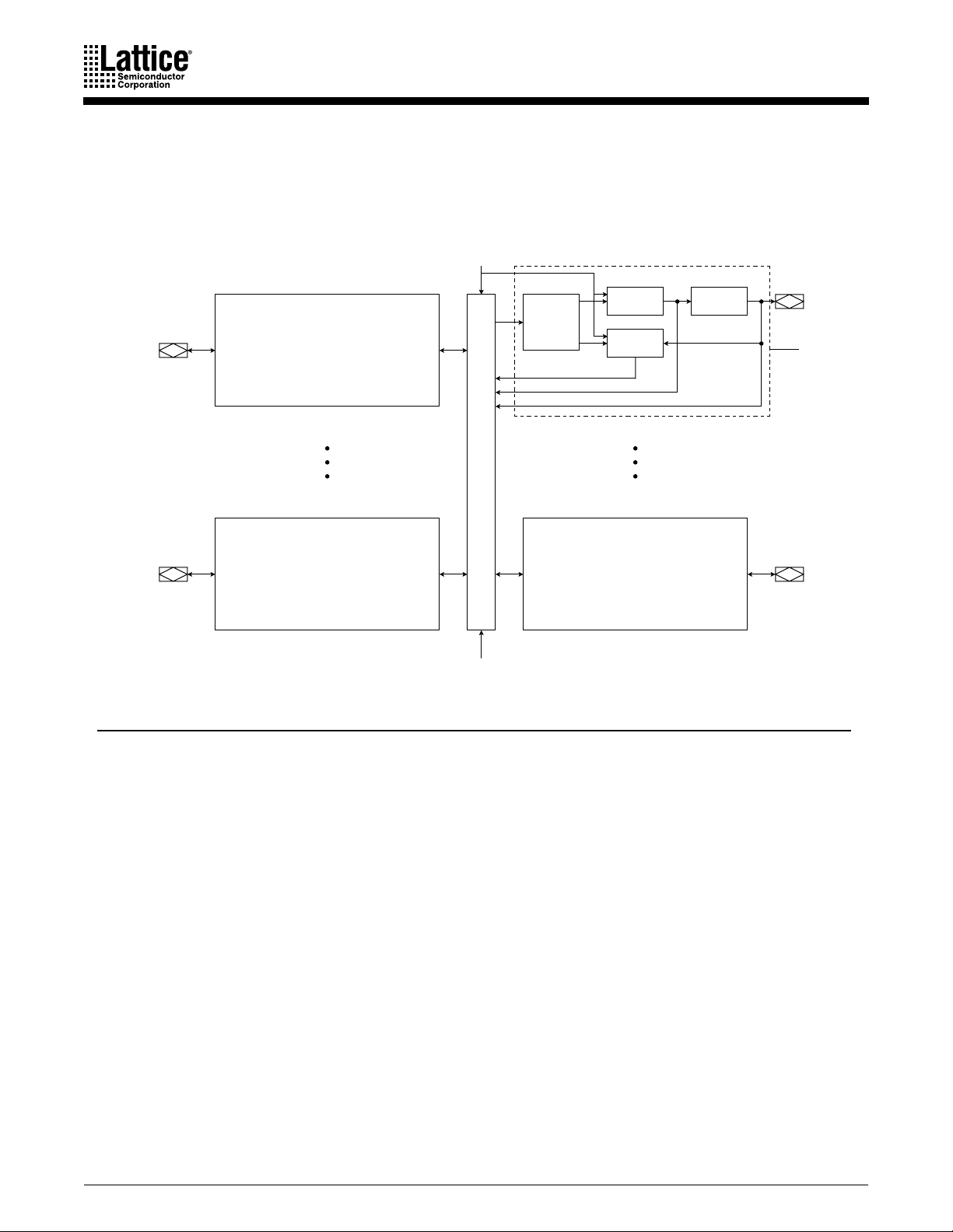
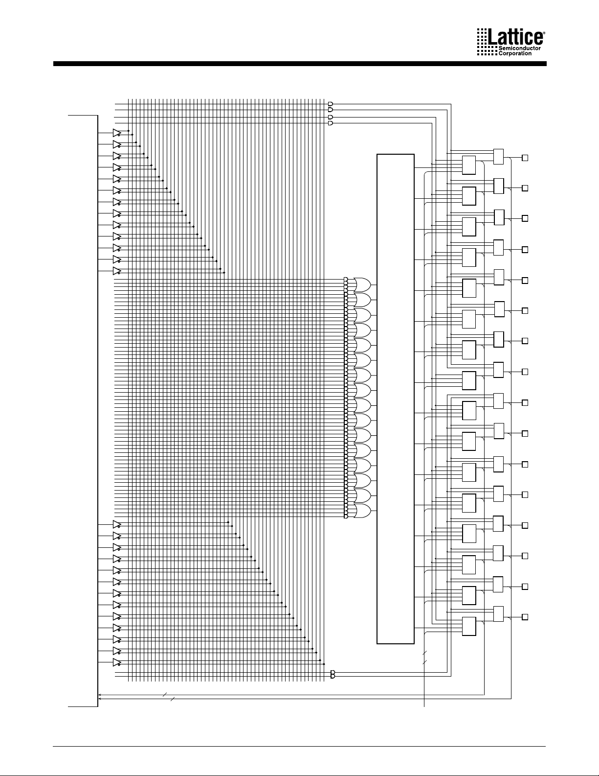
1
FUNCTIONAL DESCRIPTION
Each MACH 1 and 2 device consists of multiple, optimized P AL
matrix. The switch matrix allows communication between P AL blocks, and routes inputs to the P AL
blocks. Together , the P AL blocks and switch matrix allow the logic designer to create lar ge designs
in a single device instead of using multiple devices.
Clock/Input Pins
®
blocks interconnected by a switch
Output
Array and
Allocator
I/O Pins
I/O Pins
Note:
. There are no buried macrocells in MACH 1 devices. All macrocells are output macrocells.
Device PAL Blocks Macrocells per Block I/Os per Block Product Terms per Block
MACH111(SP) 21616 70
MACH131(SP) 41616 70
MACH211(SP) 416 8 68
MACH221(SP) 812 6 52
MACH231(SP) 816 8 68
PAL Block
Buried Macrocell Feedback
Output Macrocell Feedback
I/O Pin Feedback
Switch Matrix
Dedicated Input
Macrocells
Buried
Macrocells
(note 1)
PAL Block I/O PinsPAL Block
I/O Cells
I/O Pins
PAL Block
14051K-002
Figure 1. Overall Architecture of MACH 1 & 2 Devices
The switch matrix takes all dedicated inputs and signals from the input switch matrices and routes
them as needed to the PAL blocks. Feedback signals that return to the same PAL block still must
go through the switch matrix. This mechanism ensures that PAL blocks in MACH devices
communicate with each other with guaranteed fixed timing (SpeedLocking).
The switch matrix makes a MACH device more advanced than simply several PAL devices on a
single chip. It allows the designer to think of the device not as a collection of blocks, but as a
single programmable device; the software partitions the design into PAL blocks through the
central switch matrix so that the designer does not have to be concerned with the internal
architecture of the device.
4 MACH 1 & 2 Families
Each PAL block consists of the following elements:
◆
Product-term array
◆
Logic Allocator
◆
Macrocells
◆
I/O cells
Each PAL block additionally contains an asynchronous reset product term and an asynchronous
preset product term. This allows the flip-flops within a single P AL block to be initialized as a bank.
There are also output enable product terms that provide tri-state control for the I/O cells.
Product-Term Array
The product-term array consists of a number of product terms that form the basis of the logic being
implemented. The inputs to the AND gates come from the switch matrix (Table 4), and are
provided in both true and complement forms for efficient logic implementation.
Because the number of product terms available for a given function is not fixed, the full sum of
products is not realized in the array. The product terms drive the logic allocator, which allocates
the appropriate number of product terms to generate the function.
Table 4. PAL Block Inputs
Device Number of Inputs to PAL Block Device Number of Inputs to PAL Block
MACH111
MACH111SP
MACH131
MACH131SP
MACH211
26
26
26
26
26
MACH211SP
MACH221
MACH221SP
MACH231
MACH231SP
26
26
26
32
32
Logic Allocator
The logic allocator (Figure 2) is a block within which different product terms are allocated to the
appropriate macrocells in groups of four product terms called “product term clusters”. The
availability and distribution of product term clusters is automatically considered by the software as
it fits functions within the PAL block. The size of the product term clusters has been designed to
provide high utilization of product terms. Complex functions using many product terms are
possible, and when few product terms are used, there will be a minimal number of unused, or
wasted, product terms left over.
The product term clusters do not “wrap” around the logic block. This means that the macrocells
at the ends of the block have fewer product terms available (Tables 5, 6, 7, 8).
MACH 1 & 2 Families 5
To
n-2Ton-1
From
n-1
*
n
Product Term
Cluster
To
From
n+1
n+1
Logic
Allocator
n
*
From
n+2
*MACH 2 only
To Macrocell
n
14051K-003
Figure 2. Product Term Clusters and the Logic Allocator
Table 5. Logic Allocation for MACH111(SP)
Output Macrocell Available Clusters Output Macrocell Available Clusters
C
M
0
M
1
M
2
M
3
M
4
M
5
M
6
M
7
, C
0
1
C
, C
, C
0
1
2
C
, C
, C
1
2
3
C
, C
, C
2
3
4
C
, C
, C
3
4
5
C
, C
, C
4
5
6
C
, C
, C
5
6
7
C
, C
6
7
M
8
M
9
M
10
M
11
M
12
M
13
M
14
M
15
C
C
C
C
C
C
10,
11,
12,
13,
C
8,
C
9,
C
14, C15
C
8,
9
C
C
9,
10
C
10,
11
C
C
11,
12
C
C
12,
13
C
C
13,
14
C
C
14,
15
Table 6. Logic Allocation for MACH131(SP)
Output Macrocell Available Clusters Output Macrocell Available Clusters
M
0
M
1
M
2
M
3
M
4
M
5
M
6
M
7
C0, C
C0, C1, C
C1, C2, C
C2, C3, C
C3, C4, C
C4, C5, C
C5, C6, C
C6, C7, C
1
2
3
4
5
6
7
8
M
8
M
9
M
10
M
11
M
12
M
13
M
14
M
15
6 MACH 1 & 2 Families
C7, C8, C
C8, C9, C
, C10, C
C
9
C10, C11, C
C11, C12, C
C12, C13, C
C13, C14, C
C14, C
9
10
11
12
13
14
15
15
Table 7. Logic Allocation for MACH211(SP) and MACH231(SP)
M
0
M
2
M
4
M
6
M
0
M
2
M
4
Macrocell
Macrocell
Macrocell
Available Clusters
C0, C1, C
2
M
1
M
3
M
5
M
7
C0, C1, C2, C
C1, C2, C3, C
C2, C3, C4, C
C3, C4, C5, C
C4, C5, C6, C
C5, C6, C7, C
C6, C7, C8, C
3
4
5
6
7
8
9
M
8
M
9
M
10
M
11
M
12
M
13
M
14
M
15
Available ClustersOutput Buried Output Buried
C7, C8, C9, C
C8, C9, C10, C
C9, C10, C11, C
C10, C11, C12, C
C11, C12, C13, C
C12, C13, C14, C
C13, C14, C
C14, C
10
11
12
13
14
15
15
15
Table 8. Logic Allocation for MACH221(SP)
Macrocell
Available Clusters
C0, C1, C
2
M
1
M
3
M
5
C0, C1, C2, C
C1, C2, C3, C
C2, C3, C4, C
C3, C4, C5, C
C4, C5, C6, C
3
4
5
6
7
M
6
M
7
M
8
M
9
M
10
M
11
Available ClustersOutput Buried Output Buried
C5, C6, C7, C
C6, C7, C8, C
C7, C8, C9, C
C8, C9, C10, C
C9, C10, C
C10, C
8
9
10
11
11
11
Macrocell
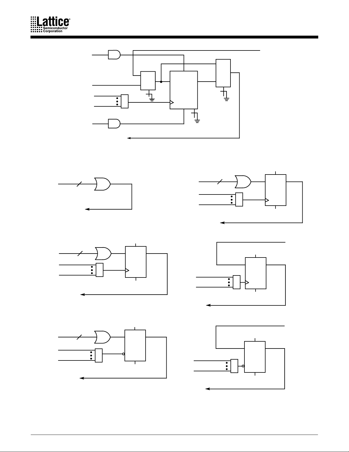
There are two fundamental types of macrocell: the output macrocell and the buried macrocell. The
buried macrocell is only found in MACH 2 devices. The use of buried macrocells effectively
doubles the number of macrocells available without increasing the pin count.
Both macrocell types can generate registered or combinatorial outputs. For the MACH 2 series,
a transparent-low latch configuration is provided. If the register is used, it can be configured as
a T-type or a D-type flip-flop. Register and latch functionality is defined in Table 9.
Programmable polarity (for output macrocells) and the T-type flip-flop both give the software a
way to minimize the number of product terms needed. These choices can be made automatically
by the software when it fits the design into the device.
Table 9. Register/Latch Operation
Configuration D/T CLK/LE Q+
X 0,1,↓ Q
D-Register
T-Register
Latch
0 ↑ 0
1 ↑ 1
X 0,1,↓ Q
0 ↑ Q
1 ↑ Q
X1Q
000
101
MACH 1 & 2 Families 7
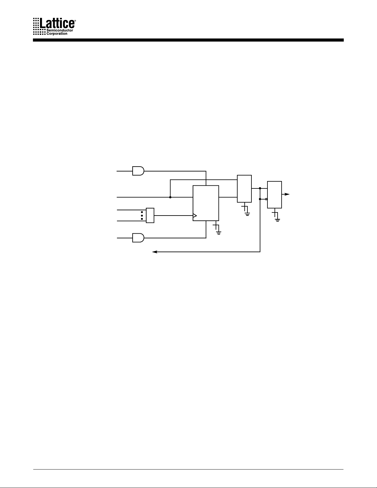
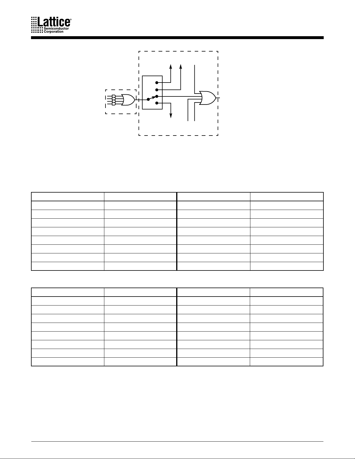
The output macrocell (Figure 3) sends its output back to the switch matrix, via internal feedback,
and to the I/O cell. The feedback is always available regardless of the configuration of the I/O cell.
This allows for buried combinatorial or registered functions, freeing up the I/O pins for use as
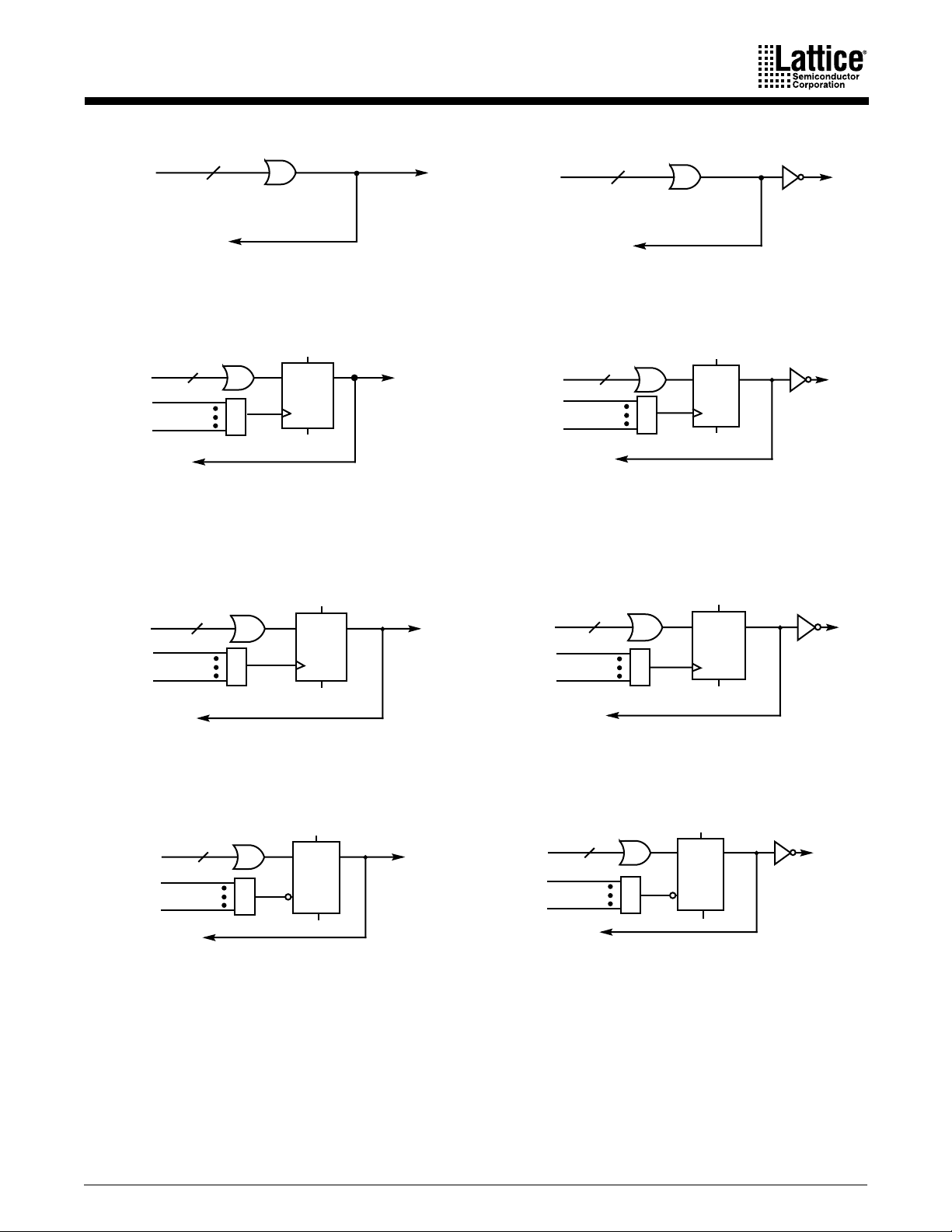
inputs if not needed as outputs. The basic output macrocell configurations are shown in Figure 4.
The buried macrocell (Figure 5) does not send its output to an I/O cell. The output of a buried
macrocell is provided only as an internal feedback signal which feeds the switch matrix. This
allows the designer to generate additional logic without requiring additional pins. The buried
macrocell can also be used to register or latch inputs. The input register is a D-type flip-flop; the
input latch is a transparent-low D-type latch. Once configured as a registered or latched input, the
buried macrocell cannot generate logic from the product-term array. The basic buried macrocell
configurations are shown in Figure 6.
PAL-Block
Asynchronous
Sum of Products
Preset
from Logic
Allocator
CLK
CLK
1
AP
1
QD/T/L
0
n
AR
0
1
To I/O
Cell
0
PAL-Block
Asynchronous
Note:
1. Latch option available on MACH 2 devices only.
Reset
To
Switch
Matrix
Figure 3. Output Macrocell
14051K-004
8 MACH 1 & 2 Families
From
Logic
Allocator
n
To
I/O
Cell
From
Logic
Allocator
n
To
I/O
Cell
From
Logic
Allocator
CLK
CLK
To Switch
From
Logic
Allocator
CLK
CLK
To Switch
To Switch
Matrix
a. Combinatorial, active high
n
0
n
Matrix
c. D-type register, active high
DQ
n
0
n
Matrix
AP
AR
T
AP
AR
To Switch
Matrix
b. Combinatorial, active low
To
I/O
Cell
Q
To
I/O
Cell
From
Logic
Allocator
CLK
CLK
From
Logic
Allocator
CLK
CLK
0
n
To Switch
Matrix
0
n
To Switch
Matrix
n
d. D-type register, active low
n
AP
DQ
AR
AP
Q
T
AR
To
I/O
Cell
To
I/O
Cell
e. T-type register, active high
From
Logic
Allocator
CLK
0
CLK
n
To Switch
Matrix
g. Latch, active high (MACH 2 only)
n
From
AP
L
Q
G
AR
To
I/O
Cell
Logic
Allocator
CLK
CLK
0
n
To Switch
Matrix
h. Latch, active low (MACH 2 only)
Figure 4. Output Macrocell Configurations
MACH 1 & 2 Families 9
f. T-type register, active low
n
AP
Q
L
G
AR
To
I/O
Cell
14051K-005
PAL-Block
From I/O Pin
Asynchronous
Preset
1
Sum of Products
From
Logic
Allocator
From Logic
Allocator
CLK
CLK
From
Logic
Allocator
CLK
0
CLK
n
From Logic
IC Allocator
PAL-Block
Asynchronous
Reset
n
To Switch
Matrix
n
0
n
To Switch
Matrix
To Switch
Matrix
CLK
0
CLK
n
Switch
Matrix
a. Combinatorial
c. T-type register
n
e. Latch
1
0
AP
QD/T/L
0
AR
To
Figure 5. Buried Macrocell (MACH 2 only)
AP
TQ
AR
AP
LQ
G
AR
From Logic
Allocator
CLKÂ
CLÂK
CLK
0
CLK
n
To Switch
Matrix
CLK
0
CLK
n
To Switch
Matrix
0
n
To Switch
n
Matrix
b. D-type register
d. Input register
f. Input latch
DQ
AP
DQ
AR
AP
LQ
G
AR
14051K-030
AP
AR
From I/O
Cell
From I/O
Cell
14051K-006
Figure 6. Buried Macrocell Configurations (MACH 2 only)
10 MACH 1 & 2 Families
The flip-flops in either macrocell type can be clocked by one of several clock pins (Table 10).
Registers are clocked on the rising edge of the clock input. Latches hold their data when the gate
input is HIGH. Clock pins are also available as inputs, although care must be taken when a signal
acts as both clock and input to the same device.
Table 10. Macrocell Clocks
Device Number of Clocks Available Device Number of Clocks Available
MACH111 4 MACH211SP 2
MACH111SP 2 MACH221 4
MACH131 4 MACH221SP 4
MACH131SP 4 MACH231 4
MACH211 4 MACH231SP 4
All flip-flops have asynchronous reset and preset. This is controlled by the common product terms
that control all flip-flops within a PAL block. For a single PAL block, all flip-flops, whether in an
output or a buried macrocell, are initialized together. The initialization functionality of the flip-flops
is illustrated in Table 11.
Table 11. Asynchronous Reset/Preset Operation
Configuration AR AP CLK/LE Q+
0 0 X See Table 9
Register
Latch
01 X 1
10 X 0
11 X 0
0 0 X See Table 9
0 1 0 Illegal
01 1 1
1 0 0 Illegal
10 1 0
1 1 0 Illegal
11 1 0
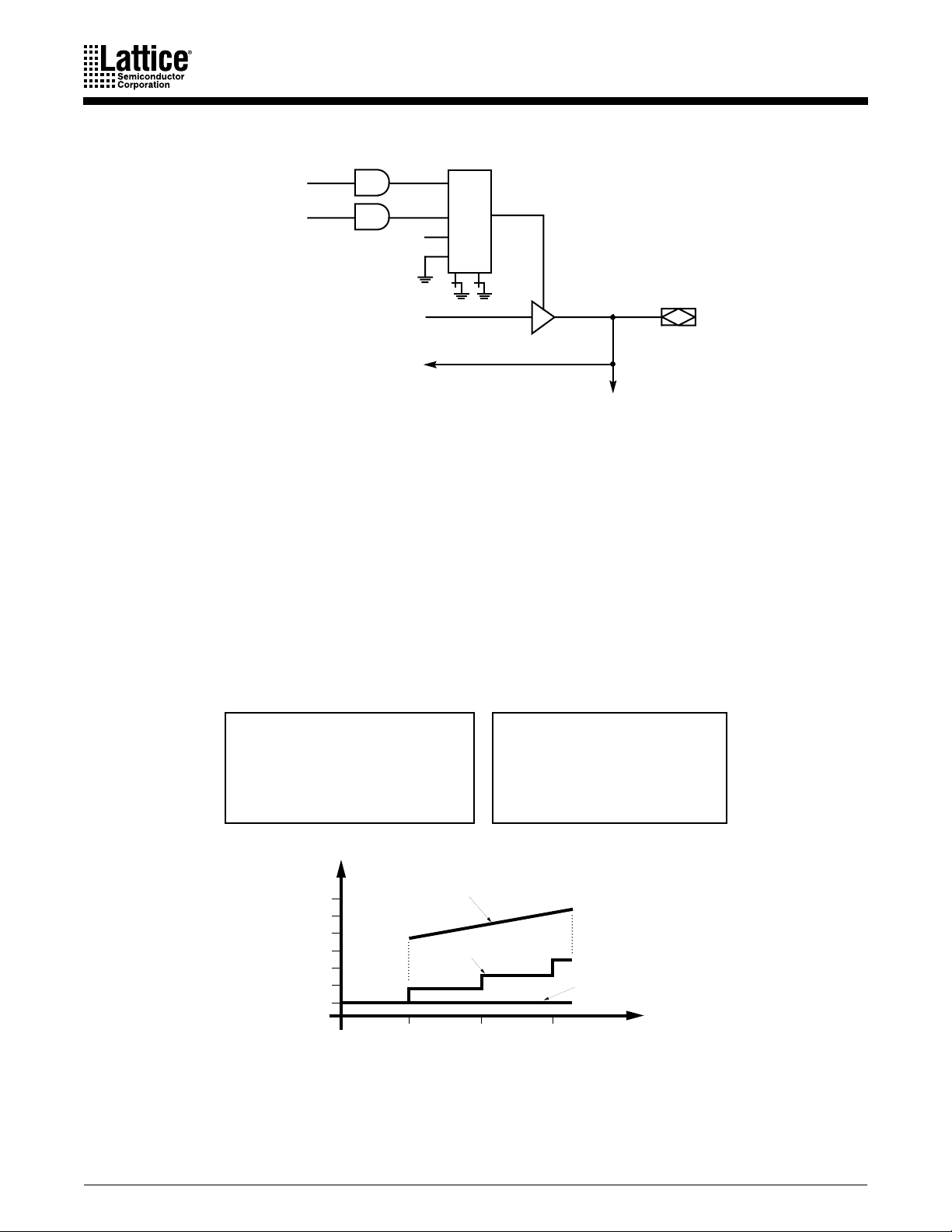
I/O Cells
The I/O cells (Figure 7) provide a three-state output buffer. The three-state buffer can be left
permanently enabled for use only as an output, permanently disabled for use as an input, or it can
be controlled by one of two product terms for bi-directional signals and bus connections. The two
product terms provided are common to a bank of I/O cells.
MACH 1 & 2 Families 11
Output Enable
Product Terms
(Common to bank of
I/O Cells)
V
CC
From Output
Macrocell
To Switch
Matrix
01
11
10
00
To Buried
Macrocell
(MACH 2 only)
14051K-007
Figure 7. I/O Cell
SPEEDLOCKING FOR GUARANTEED FIXED TIMING
The unique MACH 1 & 2 architecture is designed for high performance—a metric that is met in
both raw speed, and even more importantly, guaranteed fixed speed. The design of the switch
matrix and P AL blocks guarantee a fixed pin-to-pin delay that is independent of the logic required
by the design. Other non-Lattice/V antis CPLDs incur serious timing delays as product terms expand
beyond their typical 4 or 5 product term limits (Figure 8). Speed and SpeedLocking combine to
give designers easy access to the performance required in today’s designs.
MACH 1 & 2 SpeedLocking
• Patented Architecture
• Path Independent
• Logic/Routing Independent
• Guaranteed Fixed Timing
• Up to 16 Product Terms per Output
• Variab le
• Path Dependent
• Logic/Routing Dependent Delays
• Unpredictable
• 4-5 Product Terms before Delays
Non-MACH
SpeedLocking
Shared Expander Delay
8.8 ns
Parallel Expander Delay
6.6 ns
5.8 ns
5 ns
5 PT 10 PT 15 PT
Product Terms
t
PD
(ns)
11
10
9
8
7
6
5
Figure 8. Timing in MACH 1 & 2 vs. Non-MACH Devices
12 MACH 1 & 2 Families
10.4 ns
Non-MACH
7.4 ns
MACH 1 & 2
14051K-001

JTAG IN-SYSTEM PROGRAMMING
Programming devices in-system provides a number of significant benefits including: rapid
prototyping, lower inventory levels, higher quality, and the ability to make in-field modifications.
All MACHxxxSP devices provide in-system programming (ISP) capability through their JT AG ports.
This capability has been implemented in a manner that insures that the JTAG port remains
compliant to the IEEE 1149.1 standard. By using JTAG as the communication interface through
which ISP is achieved, customers benefit from a standard, well-defined interface.
MACHxxxSP devices can be programmed across the commercial temperature and voltage range.
These devices tristate the outputs during programming. Lattice/Vantis provides its free PC-based
Lattice/VantisPRO software to facilitate in-system programming. Lattice/VantisPRO software takes
the JEDEC file output produced by V antis’ design implementation software, along with information
about the JTAG chain, and creates a set of vectors that are used to drive the JTAG chain. Lattice/
VantisPRO software can use these vectors to drive a JTAG chain via the parallel port of a PC.
Alternatively, Lattice/VantisPRO software can output files in formats understood by common
automated test equipment. This equipment can then be used to program MACHxxxSP devices
during the testing of a circuit board. For more information about in-system programming, refer to
the separate document entitled MACH ISP Manual.
BUS-FRIENDLY INPUTS AND I/Os
The MACH 1 & 2 inputs and I/Os include two inverters in series which loop back to the input.
This double inversion weakly holds the input at its last driven logic state. For the circuit diagram,
please refer to the Input/Output Equivalent Schematics (page 393) in the General Information
Section of the Vantis 1999 Data Book.
PCI COMPLIANT
The MACH 1 & 2 families in -5/-6/-7/-10/-12 speed grades are fully compliant with the PCI Local
Bus Specification published by the PCI Special Interest Group. The MACH 1 & 2 families’
predictable timing ensures compliance with the PCI AC specifications independent of the design.
POWER-DOWN MODE
The MACH 1 & 2 families feature a programmable low-power mode in which individual signal
paths can be programmed for low power. These low-power speed paths will be slower than the
non-low-power paths. This feature allows speed critical paths to run at maximum frequency while
the rest of the paths operate in the low-power mode, resulting in power savings of up to 75%. If
all of the signals in a PAL block are in low-power mode, then the total power is reduced even
further.
SAFE FOR MIXED SUPPLY VOLTAGE SYSTEM DESIGNS
All MACHxxxSP and most of the MACH 1 & 2 devices are safe for mixed supply voltage system
designs. These 5-V devices will not overdrive 3.3-V devices above the output voltage of 3.3 V,
while they can accept inputs from other 3.3-V devices. The MACH 1 & 2 families provide easy-touse mixed-voltage design compatibility. For more information, refer to the Technical Note entitled
Mixed Supply Design with MACH 1 & 2 SP Devices.
POWER-UP RESET
All flip-flops power-up to a logic LOW for predictable system initialization. The actual values of
the outputs of the MACH devices will depend on the configuration of the macrocell. To guarantee
MACH 1 & 2 Families 13

initialization values, the VCC rise must be monotonic and the clock must be inactive until the reset
delay time has elapsed.
SECURITY BIT
A security bit is provided on the MACH devices as a deterrent to unauthorized copying of the array
configuration patterns. Once programmed, this bit defeats readback of the programmed pattern by
a device programmer, securing proprietary designs from competitors. Programming and
verification are also defeated by the security bit. The bit can only be reset by erasing the entire
device.
14 MACH 1 & 2 Families
MACH111(SP) AND MACH131(SP) PAL BLOCK
0 4 8 12 16 20 24 28 40324336
47
51
Output Enable
Output Enable
Asynchronous Reset
Asynchronous Preset
Switch
Matrix
0
63
0 4 8 12 16 20 24 28 40324336
16
16
I/O
Output
M
0
M
1
M
2
M
3
C
0
M
C
C
C
C
C
C
C
C
C
C
C
C
C
C
C
for MACH111, MACH131, MACH131SP
Output Enable
47
Output Enable
51
4
1
2
M
5
3
4
M
6
5
6
M
7
7
Logic Allocator
8
M
8
9
10
M
9
11
12
M
10
13
14
M
15
11
M
12
M
13
M
14
M
15
for MACH111SP
CLK
2
4
Macro
Cell
Output
Macro
Cell
Output
Macro
Cell
Output
Macro
Cell
Output
Macro
Cell
Output
Macro
Cell
Output
Macro
Cell
Output
Macro
Cell
Output
Macro
Cell
Output
Macro
Cell
Output
Macro
Cell
Output
Macro
Cell
Output
Macro
Cell
Output
Macro
Cell
Output
Macro
Cell
Output
Macro
Cell
Cell
I/O
Cell
I/O
Cell
I/O
Cell
I/O
Cell
I/O
Cell
I/O
Cell
I/O
Cell
I/O
Cell
I/O
Cell
I/O
Cell
I/O
Cell
I/O
Cell
I/O
Cell
I/O
Cell
I/O
Cell
I/O
I/O
I/O
I/O
I/O
I/O
I/O
I/O
I/O
I/O
I/O
I/O
I/O
I/O
I/O
I/O
14051K-013
MACH 1 & 2 Families 15

MACH211(SP) PAL BLOCK
0 4 8 12 16 20 24 28 40324336
47
51
Output Enable
Output Enable
Asynchronous Reset
Asynchronous Preset
Switch
Matrix
I/O
Output
Macro
M
0
M
1
M
2
M
3
0
63
C
0
M
C
1
C
2
M
C
3
C
4
M
C
5
C
6
M
C
7
C
Logic Allocator
8
M
C
9
C
10
M
C
11
C
12
M
C
10
13
C
14
C
M
15
11
M
12
4
5
6
7
8
9
Cell
Buried
Macro
Cell
Output
Macro
Cell
Buried
Macro
Cell
Output
Macro
Cell
Buried
Macro
Cell
Output
Macro
Cell
Buried
Macro
Cell
Output
Macro
Cell
Buried
Macro
Cell
Output
Macro
Cell
Buried
Macro
Cell
Output
Macro
Cell
Cell
I/O
Cell
I/O
Cell
I/O
Cell
I/O
Cell
I/O
Cell
I/O
Cell
I/O
I/O
I/O
I/O
I/O
I/O
I/O
0 4 8 12 16 20 24 28 40324336
16
8
47
51
16 MACH 1 & 2 Families
M
13
M
14
M
15
for MACH211SP
for MACH211
Buried
Macro
Cell
I/O
Output
Macro
Cell
Buried
Macro
Cell
CLK
2
4
Cell
I/O
14051K-015

MACH221(SP) PAL BLOCK
Switch
Matrix
0 4 8 12 16 20 24 28 40324336
0
47
47
51
Output Enable
Output Enable
Asynchronous Reset
Asynchronous Preset
M
M
M
C
0
C
1
M
C
2
C
3
M
C
4
C
5
M
C
6
C
7
M
C
Logic Allocator
8
C
9
M
C
10
C
11
M
I/O
Output
Macro
0
1
2
3
4
5
6
7
8
Cell
Buried
Macro
Cell
Output
Macro
Cell
Buried
Macro
Cell
Output
Macro
Cell
Buried
Macro
Cell
Output
Macro
Cell
Buried
Macro
Cell
Output
Macro
Cell
Cell
I/O
Cell
I/O
Cell
I/O
Cell
I/O
Cell
I/O
I/O
I/O
I/O
I/O
0 4 8 12 16 20 24 28 40324336
12
6
MACH 1 & 2 Families 17
Buried
M
9
M
10
M
11
47
51
CLK
4
Macro
Cell
Output
Macro
Cell
Buried
Macro
Cell
I/O
Cell
I/O
14051K-016

MACH231(SP) PAL BLOCK
0 4 8 12 16 20 24 28 40324336
51 55 63
47
59
Output Enable
Output Enable
Asynchronous Reset
Asynchronous Preset
Switch
Matrix
I/O
Cell
Output
Macro
M
0
M
1
M
2
M
3
M
4
M
0
63
C
0
C
1
M
C
2
C
3
M
C
4
C
5
M
Logic Allocator
C
6
C
7
M
C
8
C
9
M
10
C
10
C
11
M
C
11
12
C
13
M
C
12
14
C
15
M
13
M
14
5
6
7
8
9
Cell
Buried
Macro
Cell
Output
Macro
Cell
Buried
Macro
Cell
Output
Macro
Cell
Buried
Macro
Cell
Output
Macro
Cell
Buried
Macro
Cell
Output
Macro
Cell
Buried
Macro
Cell
Output
Macro
Cell
Buried
Macro
Cell
Output
Macro
Cell
Buried
Macro
Cell
Output
Macro
Cell
I/O
Cell
I/O
Cell
I/O
Cell
I/O
Cell
I/O
Cell
I/O
Cell
I/O
Cell
I/O
I/O
I/O
I/O
I/O
I/O
I/O
I/O
0 4 8 12 16 20 24 28 40324336
16
8
47
51
55 59 63
18 MACH 1 & 2 Families
Buried
M
15
CLK
4
Macro
Cell
14051K-017

BLOCK DIAGRAM (MACH111, MACH111SP)
Block A
I/O0 – I/O
15
CLK0 /I
CLK1 /I
CLK2/I
CLK3 /I
CLK0 /I
CLK1 /I
1
2
4
5
0
1
MACH111
MACH111SP
4
Macrocells
OE
AND Logic Array
Logic Allocator
AND Logic Array
Logic Allocator
OE
16
I/O Cells
16
52 x 70
and
26
26
52 x 70
and
16
4 MACH111
2 MACH111SP
16
Switch Matrix
4
Macrocells
16
I/O Cells
16
2 MACH111 Only
16
16
I/O16 – I/O
Block B
31
I
0
I
3
MACH111
14051K-008
MACH 1 & 2 Families 19

BLOCK DIAGRAM (MACH131, MACH131SP)
Block A Block B
4
OE
AND Logic Array
Logic Allocator
AND Logic Array
Logic Allocator
I/O
– I/O
0
15
16
I/O Cells
16 16
16
Macrocells
4
4
OE
52 x 70
AND Logic Array
and
Logic Allocator
26
Switch Matrix
26
52 x 70
AND Logic Array
and
Logic Allocator
I/O
– I/O
16
I/O Cells
Macrocells
52 x 70
and
26
26
52 x 70
and
31
16
16
I2, I
2
4
5
4
OE
Macrocells
4
16 16
16
I/O Cells
16
I/O
– I/O
48
63
Block D Block C
OE
4
4
Macrocells
16
4
I/O Cells
16
I/O
32
– I/O
47
CLK
, CLK1/I
0/I0
CLK2/I3, CLK3/I
1
4
14051K-009
20 MACH 1 & 2 Families

BLOCK DIAGRAM (MACH211, MACH211SP)
Block A Block B
I/O0–I/O
7
I/O
–I/O
8
15
MACH211 only
CLK0 /I
CLK1 /I
CLK2/I
CLK3 /I
CLK0 /I
CLK1 /I
1
2
4
5
0
1
MACH211
MACH211SP
I/O Cells
8
Macrocells
Macrocells
8
I/O Cells
8
8
8
Macrocells
I/O Cells
8
Macrocells
2 2
OE
52 x 68
AND Logic
Array
and
26
Switch Matrix
26
52 x 68
AND Logic Array
and
Logic Allocator
OE
2 2
Macrocells
8
8
Macrocells
8
I/O Cells
8
8
8
Macrocells
OE
52 x 68
AND Logic
Amrray
and
26
26
52 x 68
AND Logic Array
and
Logic Allocator
OE
Macrocells
8
8
2 MACH211SP
4 MACH211
8
8
2 MACH211 only
I/O
24
–I/O
I/O
31
16
–I/O
23
Block D Block C
MACH 1 & 2 Families 21
I
0
3
MACH211
14051K-010
I

BLOCK DIAGRAM (MACH221, MACH221SP
)
,
7
3
–I
–I
6
2
I
I
4
4
1
5
/I
/I
1
3
, CLK
, CLK
0
4
4
/I
0
CLK
4
/I
2
CLK
Block DBlock CBlock BBlock A
23
– I/O
18
I/O
17
– I/O
12
I/O
6
6
6
6
6
I/O Cells
6
6
6
I/O Cells
Macrocells
2
Macrocells
Macrocells
2
Macrocells
O
52 x 52
AND Logic Array
O
52 x 52
AND Logic Array
26
and Logic Allocator
26
and Logic Allocator
26
26
Switch Matrix
O
52 x 52
AND Logic Array
and Logic Allocator
O
52 x 52
222 2
AND Logic Array
and Logic Allocator
6
6
6
Macrocells Macrocells
6
6
6
Macrocells Macrocells
6
I/O Cells
6
I/O Cells
29
– I/O
24
I/O
35
– I/O
30
I/O
11
– I/O
6
I/O
5
– I/O
0
I/O
6
6
6
6
6
I/O Cells
6
6
6
I/O Cells
Macrocells
2
Macrocells
Macrocells
2
Macrocells
O
52 x 52
AND Logic Array
and Logic Allocator
O
52 x 52
AND Logic Array
and Logic Allocator
6
6
6
6
6
6
6
I/O Cells
6
I/O Cells
41
– I/O
36
I/O
47
– I/O
42
I/O
Block H Block G Block F Block E
14051K-011
26
26
26
26
O
52 x 52
AND Logic Array
and Logic Allocator
O
52 x 52
AND Logic Array
and Logic Allocator
Macrocells Macrocells
Macrocells Macrocells
22 MACH 1 & 2 Families

BLOCK DIAGRAM (MACH231, MACH231SP
)
5
, I
2
I
2
4
1
4
/I
/I
1
3
, CLK
, CLK
0
4
4
/I
0
CLK
3
/I
2
CLK
(Block D)
31
– I/O
24
I/O
(Block C)
23
– I/O
16
I/O
8
8
8
8
8
I/O Cells
8
8
8
I/O Cells
8
Macrocells
OE
Macrocells
Macrocells
OE
Macrocells
64 x 68
32
AND Logic Array
and Logic Allocator
64 x 68
32
AND Logic Array
and Logic Allocator
8
8
8
8
I/O Cells
(Block E)
39
– I/O
32
64 x 68
32
OE
2222
AND Logic Array
and Logic Allocator
Macrocells Macrocells
I/O
8
Macrocells
8
8
8
I/O Cells
(Block F)
47
– I/O
40
OE
64 x 68
32
AND Logic Array
and Logic Allocator
Switch Matrix
Macrocells
I/O
8
(Block B)
15
– I/O
8
I/O
(Block A)
7
– I/O
0
I/O
8
8
8
8
I/O Cells
8
8
8
I/O Cells
Macrocells
OE
2 2 2
Macrocells
Macrocells
OE
2
Macrocells
Macrocells
8
8
8
I/O Cells
(Block G)
55
– I/O
48
64 x 68
AND Logic Array
and Logic Allocator
OE
32
64 x 68
32
AND Logic Array
and Logic Allocator
Macrocells
I/O
8
Macrocells
8
8
8
I/O Cells
(Block
– /O
I/O
63
56
14051K-012
64 x 68
AND Logic Array
and Logic Allocator
OE
32
64 x 68
32
AND Logic Array
and Logic Allocator
Macrocells
MACH 1 & 2 Families 23

ABSOLUTE MAXIMUM RATINGS
OPERATING RANGES
Storage Temperature. . . . . . . . . . . . . .-65°C to +150°C
Ambient Temperature
With Power Applied . . . . . . . . . . . . . .-55°C to +125°C
Device Junction Temperature . . . . . . . . . . . . . +150°C
Supply Voltage with
Respect to Ground . . . . . . . . . . . . . . .-0.5 V to +7.0 V
DC Input Voltage . . . . . . . . . . . . -0.5 V to V
DC Output or I/O Pin Voltage . . -0.5 V to V
CC
+0.5 V
CC
+0.5 V
Static Discharge Voltage . . . . . . . . . . . . . . . . . 2001 V
Latchup Current (TA = -40°C to +85°C). . . . . . . 200 mA
Stresses above those listed under Absolute Maximum Ratings
may cause permanent device failure. Functionality at or above
these limits is not implied. Exposure to Absolute Maximum Ratings for extended periods may affect device reliability.
Commercial (C) Devices
Ambient Temperature (TA)
Operating in Free Air. . . . . . . . . . . . . . . 0°C to +70°C
Supply Voltage (VCC)
with Respect to Ground . . . . . . . . . +4.75 V to +5.25 V
Operating ranges define those limits between which the functionality of the device is guaranteed.
Industrial (I) Devices
Ambient Temperature (TA)
Operating in Free Air. . . . . . . . . . . . . . -40°C to +85°C
Supply Voltage (VCC)
with Respect to Ground . . . . . . . . . . . +4.5 V to +5.5 V
Operating ranges define those limits between which the
functionality of the device is guaranteed.
DC CHARACTERISTICS OVER OPERATING RANGES
Parameter
Symbol Parameter Description Test Description Min Typ Max Unit
V
V
V
V
I
I
I
I
I
OH
OL
IH
IL
IH
IL
OZH
OZL
SC
Output HIGH Voltage
Output LOW Voltage IOL = 16 mA, VCC = Min, VIN = V
Input HIGH Voltage
Input LOW Voltage
Input HIGH Leakage Current VIN = 5.25 V, V VCC = Max (Note 4) 10 µA
Input LOW Leakage Current VIN = 0 V, VCC = Max (Note 4) –10 µA
Off-State Output Leakage Current HIGH V
Off-State Output Leakage Current LOW V
Output Short-Circuit Current V
IOH = –3.2 mA, VCC = Min, VIN = V
IOH = –300 µA, VCC = Max, VIN = VIH or VIL (Note 1) 3.5 V
Guaranteed Input Logical HIGH Voltage for all Inputs
(Note 3)
Guaranteed Input Logical LOW Voltage for all Inputs
(Note 3)
= 5.25 V, VCC = Max, VIN = V
OUT
= 0 V, VCC = Max, VIN = V
OUT
= 0.5 V VCC = Max (Note 5) –30
OUT
or V
IH
IL
or V
(Note 2) 0.5 V
IH
IL
or VIL (Note 4) 10 µA
IH
or VIL (Note 4) –10 µA
IH
2.4 V
2.0 V
0.8 V
–130 (Note 6),
–160
mA
Notes:
1. This applies to MACH111SP, MACH131SP, and die code “B” or later for MACH211(SP) and MACH231(SP). This does not apply
to MACH111, MACH131, MACH221(SP), and die code “A” for MACH211(SP) and MACH231(SP).
2. Total I
3. These are absolute values with respect to device ground, and all overshoots due to system and/or tester noise are included.
4. I/O pin leakage is the worst case of I
5. Not more than one output should be shorted at a time. Duration of the short-circuit should not exceed one second.
V
6. For commercial temperature range only.
for one PAL block should not exceed 64 mA.
OL
and I
IL
= 0.5 V has been chosen to avoid test problems caused by tester ground degradation.
OUT
(or IIH and I
OZL
OZH
).
24 MACH 1 & 2 Families

MACH111 AND MACH111SP
SWITCHING CHARACTERISTICS OVER OPERATING RANGES
1
Parameter
Symbol
t
PD
t
S
t
H
t
CO
t
WL
t
WH
f
MAX
t
AR
t
ARW
t
ARR
t
AP
t
APW
t
APR
t
EA
t
ER
t
LP
t
LPS
t
LPCO
t
LPEA
-5 -7 -10 -12 -14 -15 -18
Parameter Description
UnitMin Max Min Max Min Max Min Max Min Max Min Max Min Max
Input, I/O, or Feedback to Combinatorial Output 5 7.5 10 12 14 15 18 ns
Setup Time from Input, I/O, or Feedback
to Clock
D-type 3.5 5.5 6.5 7 8.5 10 12 ns
T-type 4 6.5 7.5 8 10 11 13.5 ns
Register Data Hold Time 0000000ns
Clock to Output 3.5 5 6 8 10 10 12 ns
Clock Width
Maximum
Frequency
External
Feedback
1/(t
Internal Feedback (f
No Feedback 1/(t
+ tCO)
S
CNT
WL
LOW2.5356667.5ns
HIGH 2.5 356667.5ns
D-type 143 95 80 66.7 54 50 42 MHz
T-type 133 87 74 62.5 50 47.6 39 MHz
D-type 182 133 100 76.9 69 66.6 53 MHz
)
T-type 167 125 91 71.4 57 55.5 44 MHz
+ tWH) 200 167 100 83.3 83.3 83.3 66.7 MHz
Asynchronous Reset to Registered Output 7.5 9.5 11 16 19.5 20 24 ns
Asynchronous Reset Width (Note 2) 4.5 5 7.5 12 14.5 15 18 ns
Asynchronous Reset Recovery Time (Note 2) 4.5 5 7.5 8 10 10 12 ns
Asynchronous Preset to Registered Output 7.5 9.5 11 16 19.5 20 24 ns
Asynchronous Preset Width (Note 2) 4.5 5 7.5 12 14.5 15 18 ns
Asynchronous Preset Recovery Time (Note 2) 4.5 5 7.5 8 10 10 12 ns
Input, I/O, or Feedback to Output Enable 7.5 9.5 10 12 14.5 15 18 ns
Input, I/O, or Feedback to Output Disable 7.5 9.5 10 12 14.5 15 18 ns
tPD Increase for Powered-down Macrocell (Note 3) 10 10 10 10 10 10 10 ns
tS Increase for Powered-down Macrocell (Note 3) 7777777ns
tCO Increase for Powered-down Macrocell (Note 3) 3333333ns
tEA Increase for Powered-down Macrocell (Note 3) 10 10 10 10 10 10 10 ns
Notes:
1. See “Switching Test Circuit” in the General Information Section of the Vantis 1999 Data Book.
2. These parameters are not 100% tested, but are evaluated at initial characterization and at any time the design is modified where this parameter may be affected.
3. If a signal is powered-down, this parameter must be added to its respective high-speed parameter.
MACH 1 & 2 Families 25

MACH131 AND MACH131SP
SWITCHING CHARACTERISTICS OVER OPERATING RANGES
1
Parameter
Symbol
t
PD
t
S
t
H
t
CO
t
WL
t
WH
f
MAX
t
AR
t
ARW
t
ARR
t
AP
t
APW
t
APR
t
EA
t
ER
t
LP
t
LPS
t
LPCO
t
LPEA
-5 -7 -10 -12 -14 -15 -18
Parameter Description
UnitMin Max Min Max Min Max Min Max Min Max Min Max Min Max
Input, I/O, or Feedback to Combinatorial Output 5.5 7.5 10 12 14 15 18 ns
D-type 3.0 5.5 6.5 7 8.5 10 12 ns
Setup Time from Input, I/O, or Feedback
T-type 3.5 6.5 7.5 8 10 11 13.5 ns
Hold Time 0000000ns
Clock to Output 4568101012ns
LOW2.5346667.5ns
Clock Width
HIGH 2.5 346667.5ns
D-type 143 95 80 66.7 54 50 42 MHz
+ tCO)
T-type 133 87 74 62.5 50 47.6 39 MHz
D-type 182 133 100 76.9 69 66.6 53 MHz
)
CNT
T-type 167 125 91 71.4 57 55.5 44 MHz
+ tWH) 200 167 125 83.3 83.3 83.3 66.7 MHz
Maximum
Frequency
External
Feedback
1/(t
Internal Feedback (f
No
Feedback
1/(t
WL
S
Asynchronous Reset to Registered Output 8.5 9.5 11 16 19.5 20 24 ns
Asynchronous Reset Width (Note 2) 4.5 5 7.5 12 14.5 15 18 ns
Asynchronous Reset Recovery Time (Note 2) 4.5 5 7.5 8 10 10 12 ns
Asynchronous Preset to Registered Output 8.5 9.5 11 16 19.5 20 24 ns
Asynchronous Preset Width (Note 2) 4.5 5 7.5 12 14.5 15 18 ns
Asynchronous Preset Recovery Time (Note 2) 4.5 5 7.5 8 10 10 12 ns
Input, I/O, or Feedback to Output Enable 7.5 9.5 10 12 14.5 15 18 ns
Input, I/O, or Feedback to Output Disable 7.5 9.5 10 12 14.5 15 18 ns
tPD Increase for Powered-Down Macrocell (Note 3) 10 10 10 10 10 10 10 ns
tS Increase for Powered-Down Macrocell (Note 3) 7777777ns
tCO Increase for Powered-Down Macrocell (Note 3) 3333333ns
tEA Increase for Powered-Down Macrocell (Note 3) 10 10 10 10 10 10 10 ns
Notes:
1. See “Switching Test Circuit” in the General Information Section of the Vantis 1999 Data Book..
2. These parameters are not 100% tested, but are evaluated at initial characterization and at any time the design is modified where
this parameter may be affected.
3. If a signal is powered down, this parameter must be added to its respective high-speed parameter.
26 MACH 1 & 2 Families

MACH211 AND MACH211SP
SWITCHING CHARACTERISTICS OVER OPERATING RANGES
1
Parameter
Symbol Parameter Description
t
PD
t
S
t
H
t
CO
t
WL
t
WH
f
MAX
t
SL
t
HL
t
GO
t
GWL
t
PDL
t
SIR
t
HIR
t
ICO
t
ICS
t
WICL
t
WICH
f
MAXIR
t
SIL
t
HIL
t
IGO
t
IGOL
t
SLL
t
IGS
t
WIGL
t
PDLL
Input, I/O, or Feedback to Combinatorial
Output
Setup Time from Input, I/O, or Feedback
to Clock
Register Data Hold Time 0 0 0 0000 ns
Clock to Output 4 4.5 6 8 10 10 12 ns
Clock Width
External
Feedback
Maximum
Frequency
Setup Time from Input, I/O, or Feedback to Gate 5 5.5 6.5 7 8.5 10 12 ns
Latch Data Hold Time 0 0 0 0000 ns
Gate to Output 7
Gate Width LOW 2.5 3 5 6 6 6 7.5 ns
Input, I/O, or Feedback to Output Through
Transparent Input or Output Latch
Input Register Setup Time 1.5 2 2 2 2 2 2.5 ns
Input Register Hold Time 1.5 2 2 2 2.5 2.5 3.5 ns
Input Register Clock to Combinatorial Output 10 11 13 15 18 18
Input Register Clock to Output Register
Setup
Input Register
Clock Width
Maximum Input Register
Frequency
Input Latch Setup Time 1.5 2 2 2 2 2 2.5 ns
Input Latch Hold Time 1.5 2 2 2 2.5 2.5 3.5 ns
Input Latch Gate to Combinatorial Output 12 12 14 17 20 20 24 ns
Input Latch Gate to Output Through Transparent
Output Latch
Setup Time from Input, I/O, or Feedback Through
Transparent Input Latch to Output Latch Gate
Input Latch Gate to Output Latch Setup 9 10 11 13 16 16 19.5 ns
Input Latch Gate Width LOW 2.5 3 5 6 6 6 7.5 ns
Input, I/O, or Feedback to Output Through
Transparent Input and Output Latches
Internal Feedback (f
No Feedback 1/(tWL + tWH) 200 167 100 83.3 83.3 83.3 66.7 MHz
1/(t
1/(t
-6 -7 -10 -12 -14 -15 -18
6 7.5 10 12 14 15 18 ns
D-type 5 5.5 6.5 7 8.5 10 12 ns
T-type 5.5 6.5 7.5 8 10 11 13.5 ns
LOW 2.5 3 5 6 6 6 7.5 ns
HIGH 2.5 3 5 6 6 6 7.5 ns
D-type 111 100 80 66.7 54 50 42 MHz
+ tCO)
S
T-type 105 91 74 62.5 50 47.6 39 MHz
D-type 166 133 100 83.3 69 66.6 55.6 MHz
)
CNT
T-type 150 125 91 76.9 62.5 62.5 51.3 MHz
7
7.5
(note 4)
9 9.5 12 14 17 17
D-type 8 9 10 12 14.5 15 18 ns
T-type 9 10 11 13 16 16 19.5 ns
LOW 2.5 3 5 6 6 6 7.5 ns
HIGH 2.5 3 5 6 6 6 7.5 ns
+ t
WICL
) 200 167 100 83.3 83.3 83.3 66.7 MHz
WICH
13 14 16 19 22 22 26.5 ns
7 7.5 8.5 9 11 12 14.5 ns
12 12.5 14 16 19 19 23 ns
7
8
(note 5)
10 11 11
13
(note 6)
13.5
20
(note 6)
20.5
20
(note 6)
22
UnitMin Max Min Max Min Max Min Max Min Max Min Max Min Max
ns
ns
ns
MACH 1 & 2 Families 27

MACH211 AND MACH211SP (CONTINUED)
SWITCHING CHARACTERISTICS OVER OPERATING RANGES
1
Parameter
Symbol Parameter Description
t
AR
t
ARW
t
ARR
t
AP
t
APW
t
APR
t
EA
t
ER
t
LP
t
LPS
t
LPCO
t
LPEA
Asynchronous Reset to Registered or Latched
Output
Asynchronous Reset Width (Note 2) 4 5 10 12 14.5 15 18 ns
Asynchronous Reset Recovery Time (Note 2) 4 5 10 10 10 10 12 ns
Asynchronous Preset to Registered or Latched
Output
Asynchronous Preset Width (Note 2) 4 5 10 12 14.5 15 18 ns
Asynchronous Preset Recovery Time (Note 2) 4 5 10 10 10 10 12 ns
Input, I/O, or Feedback to Output Enable 9 9.5 10 12 14 15 18 ns
Input, I/O, or Feedback to Output Disable 9 9.5 10 12 14 15 18 ns
tPD Increase for Powered-down Macrocell (Note 3) 10 10 10 10 10 10 10 ns
tS Increase for Powered-down Macrocell (Note 3) 10 10 10 10 10 10 10 ns
tCO Increase for Powered-down Macrocell (Note 3) 0 0 0 0 0 0 0 ns
tEA Increase for Powered-down Macrocell (Note 3) 10 10 10 10 10 10 10 ns
-6 -7 -10 -12 -14 -15 -18
UnitMin Max Min Max Min Max Min Max Min Max Min Max Min Max
9 9.5 15 16 19.5 20 24 ns
9 9.5 15 16 19.5 20 24 ns
Notes:
1. See “Switching Test Circuit” in the General Information Section of the Vantis 1999 Data Book.
2. These parameters are not 100% tested, but are evaluated at initial characterization and at any time the design is modified where
this parameter may be affected.
3. If a signal is powered-down, this parameter must be added to its respective high-speed parameter.
4. MACH211 t
5. MACH211, commercial t
6. The faster -18 t
= 7 ns. MACH211SP tGO = 7.5 ns.
GO
= 7 ns.
GO
, t
, t
GO
PDL
, apply to MACH211 only, not MACH211SP.
ICO
28 MACH 1 & 2 Families

MACH221 and MACH221SP
SWITCHING CHARACTERISTICS OVER OPERATING RANGES
1
Parameter
Symbol Parameter Description
t
PD
t
s
t
H
t
CO
t
WL
t
WH
f
MAX
t
SL
t
HL
t
GO
t
GWL
t
PDL
t
SIR
t
HIR
t
ICO
t
ICS
t
WICL
t
WICH
f
MAXIR
t
SIL
t
HIL
t
IGO
t
IGOL
t
SLL
t
IGS
t
WIGL
t
PDLL
t
AR
t
ARW
t
ARR
t
AP
Input, I/O, or Feedback to Combinatorial Output 7.5 10 12 14 15 18 ns
Setup Time from Input, I/O, or Feedback to
Clock
Register Data Hold Time 000000ns
Clock to Output 5 6 8 10 10 12 ns
Clock Width
External
Feedback
Maximum
Frequency
Setup Time from Input, I/O, or Feedback to Gate 5.5 6.5 7 8.5 10 12 ns
Latch Data Hold Time 000000ns
Gate to Output 7
Gate Width LOW 356667.5ns
Input, I/O, or Feedback to Output Through Transparent
Input or Output Latch
Input Register Setup Time 222222.5ns
Input Register Hold Time 2 2 2 2.5 2.5 3.5 ns
Input Register Clock to Combinatorial Output 11 13 15 18 18 22 ns
Input Register Clock to Output Register Setup
Input Register LOW 356667.5ns
Clock Width HIGH 356667.5ns
Maximum Input Register
Frequency
Input Latch Setup Time 222222.5ns
Input Latch Hold Time 2 2 2 2.5 2.5 3.5 ns
Input Latch Gate to Combinatorial Output 12 14 17 20 20 24 ns
Input Latch Gate to Output Through Transparent Output
Latch
Setup Time from Input, I/O, or Feedback Through
Transparent Input Latch to Output Latch Gate
Input Latch Gate to Output Latch Setup 10 11 13 16 16 19.5 ns
Input Latch Gate Width LOW 356667.5ns
Input, I/O, or Feedback to Output Through Transparent
Input and Output Latches
Asynchronous Reset to Registered or Latched Output 9.5 15 16 19.5 20 24 ns
Asynchronous Reset Width (Note 3) 5 10 12 14.5 15 18 ns
Asynchronous Reset Recovery Time (Note 3) 5 8 10 10 10 12 ns
Asynchronous Preset to Registered or Latched Output 9.5 15 16 19.5 20 24 ns
Internal Feedback (f
No Feedback 1/(tWL + tWH) 167 100 83.3 83.3 83.3 66.7 MHz
1/(tS + tCO)
1/(t
WICL
-7 -10 -12 -14 -15 -18
D-type 5.5 6.5 7 8.5 10 12 ns
T-type 6.5 7.5 8 10 11 13.5 ns
LOW356667.5ns
HIGH 356667.5ns
D-type 95 80 66.7 54 50 42 MHz
T-type 87 74 62.5 50 47.6 39 MHz
D-type 133 100 83.3 69 66.6 55.6 MHz
)
CNT
T-type 125 91 76.9 62.5 62.5 51.3 MHz
7
(note 2)
9.5 12 14 17 17 20.5 ns
D-type 9 10 12 14.5 15 18 ns
T-type 10 11 13 16 16 19.5 ns
+ t
) 167 100 83.3 83.3 83.3 66.7 MHz
WICH
14 16 19 22 22 26.5 ns
7.5 8.5 9 11 12 14.5 ns
11.5 14 16 19 19 23 ns
10 11 11 13.5 ns
UnitMin Max Min Max Min Max Min Max Min Max Min Max
MACH 1 & 2 Families 29

MACH221 and MACH221SP (CONTINUED)
SWITCHING CHARACTERISTICS OVER OPERATING RANGES
1
Parameter
Symbol Parameter Description
t
APW
t
APR
t
EA
t
ER
t
LP
t
LPS
t
LPCO
t
LPEA
Asynchronous Preset Width (Note 3) 5 10 12 14.5 15 18 ns
Asynchronous Preset Recovery Time (Note 3) 5 8 10 10 10 12 ns
Input, I/O, or Feedback to Output Enable 9.5 12 12 14 15 18 ns
Input, I/O, or Feedback to Output Disable 9.5 12 12 14 15 18 ns
t
Increase for Powered-down Macrocell (Note 4) 10 10 10 10 10 10 ns
PD
tS Increase for Powered-down Macrocell (Note 4) 10 10 10 10 10 10 ns
tCO Increase for Powered-down Macrocell (Note 4) 000000ns
tEA Increase for Powered-down Macrocell (Note 4) 10 10 10 10 10 10 ns
-7 -10 -12 -14 -15 -18
UnitMin Max Min Max Min Max Min Max Min Max Min Max
Notes:
1. See “Switching Test Circuits” in the General Information section of the Vantis 1999 Data Book.
2. MACH221 t
= 7 ns. MACH221SP tGO = 8 ns.
GO
3. These parameters are not 100% tested, but are evaluated at initial characterization and at any time the design is modified where
this parameter may be affected.
4. If a signal is powered-down, this parameter must be added to its respective high-speed parameter.
30 MACH 1 & 2 Families

MACH231 AND MACH231SP
SWITCHING CHARACTERISTICS OVER OPERATING RANGES
1
Parameter
Symbol Parameter Description
t
t
t
t
t
t
f
t
t
t
t
t
PD
S
H
CO
WL
WH
MAX
SL
HL
GO
GWL
PDL
Input, I/O, or Feedback to Combinatorial Output 6 7.5 10 12 14 15 18 ns
Setup Time from Input, I/O, or Feedback
to Clock
Register Data Hold Time 0000000ns
Clock to Output 4 5 6.5 8 10 10 12 ns
Clock Width
External
Feedback
Maximum
Frequency
Setup Time from Input, I/O, or Feedback to Gate 5 5.5 6.5 7 8.5 10 12 ns
Latch Data Hold Time 0000000ns
Gate to Output 5 6 7.5 8.5 11 11 13.5 ns
Gate Width LOW 2346667.5ns
Input, I/O, or Feedback to Output Through
Transparent Input or Output Latch
Internal Feedback (f
No
Feedback
1/(tS + tCO)
1/(t
WL
-6 -7 -10 -12 -14 -15 -18
UnitMin Max Min Max Min Max Min Max Min Max Min Max Min Max
D-type 5 5.5 6.5 7 8.5 10 12 ns
T-type 6 6.5 7.5 8 10 11 13.5 ns
LOW2.5346667.5ns
HIGH 2.5 346667.5ns
D-type 111 95 77 66.7 54 50 42 MHz
T-type 100 87 72 62.5 50 47.6 39 MHz
D-type 166 133 100 83.3 69 66.6 55.6 MHz
)
CNT
T-type 150 125 91 76.9 62.5 62.5 51.3 MHz
+ tWH) 200 167 125 83.3 83.3 83.3 66.7 MHz
9 9.5 14 14.5 17 17 20.5 ns
t
SIR
t
HIR
t
ICO
t
ICS
t
WICL
t
WICH
f
MAXIR
t
SIL
t
HIL
t
IGO
t
IGOL
t
SLL
t
IGS
Input Register Setup Time 1.5 222222.5ns
Input Register Hold Time 1.5 2 2.5 2.5 2.5 2.5 3.5 ns
Input Register Clock to Combinatorial Output 10 11 15.5 16 18 18 22 ns
Input Register Clock to output Register
Setup
Input Register
Clock Width
Maximum Input Register Frequency 200 167 125 83.3 83.3 83.3 66.7 MHz
Input Latch Setup Time 1.5 2 2 2.5 2.5 2.5 2.5 ns
Input Latch Hold Time 1.5 2 2.5 3 3 3 3.5 ns
Input Latch Gate to Combinatorial Output 11 12 17 17 20 20 24 ns
Input Latch Gate to Output Through Transparent
Output Latch
Setup Time from Input, I/O, or Feedback Through
Transparent Input Latch to Output Latch Gate
Input Latch Gate to Output Latch Setup 9 10 11 13.5 16 16 19.5 ns
D-type 8 9 11 12 14.5 15 18 ns
T-type 9 10 12 13 16 16 19.5 ns
LOW2.5346667.5ns
HIGH 2.5 346667.5ns
13 14 18 19.5 22 22 26.5 ns
7 7.5 10 10.5 11 12 14.5 ns
MACH 1 & 2 Families 31

MACH231 AND MACH231SP (CONTINUED)
SWITCHING CHARACTERISTICS OVER OPERATING RANGES
1
Parameter
Symbol Parameter Description
t
WIGL
t
PDLL
t
AR
t
ARW
t
ARR
t
AP
t
APW
t
APR
t
EA
t
ER
t
LP
t
LPS
t
LPCO
t
LPEA
Input Latch Gate Width LOW 2346667.5ns
Input, I/O, or Feedback to Output Through
Transparent Input and Output Latches
Asynchronous Reset to Registered or Latched
Output
Asynchronous Reset Width (Note 2) 4 5 10 12 14.5 15 18 ns
Asynchronous Reset Recovery Time
(Note 2)
Asynchronous Preset to Registered or Latched
Output
Asynchronous Preset Width (Note 2) 4 5 10 12 14.5 15 18 ns
Asynchronous Preset Recovery Time (Note 2) 4 5 7.5 8 10 10 12 ns
Input, I/O, or Feedback to Output Enable 9 9.5 10 12 15 15 18 ns
Input, I/O, or Feedback to Output Disable 9 9.5 10 12 15 15 18 ns
tPD Increase for Powered-down Macrocell (Note 3) 9 10 10 10 10 10 10 ns
tS Increase for Powered-down Macrocell (Note 3) 6777777ns
tCO Increase for Powered-down Macrocell (Note 3) 0000000ns
tEA Increase for Powered-down Macrocell (Note 3) 9 10 10 10 10 10 10 ns
-6 -7 -10 -12 -14 -15 -18
UnitMin Max Min Max Min Max Min Max Min Max Min Max Min Max
11 12.5 16 17 19 19 23 ns
9 9.5 13 16 19.5 20 24 ns
4 57.58 101012ns
9 9.5 13 16 19.5 20 24 ns
Notes:
1. See “Switching Test Circuit” in the General Information section of the Vantis 1999 Data Book.
2. These parameters are not 100% tested, but are evaluated at initial characterization and at any time the design is modified where
this parameter may be affected.
3. If a signal is powered-down, this parameter must be added to its respective high-speed parameter.
CAPACITANCE
1
Parameter Symbol Parameter Description Test Conditions Typ Unit
C
IN
C
OUT
Input Capacitance VIN = 2.0V VCC = 5.0V,
T
= 25°C
Output Capacitance V
= 2.0V 8 pF
OUT
A
f = 1 MHz
6pF
Note:
1. These parameters are not 100% tested, but are calculated at initial characterization and at any time the design is modified where
these parameters may be affected.
32 MACH 1 & 2 Families

I
vs. FREQUENCY
CC
These curves represent the typical power consumption for a particular device at system frequency.
The selected “typical” pattern is a 16-bit up-down counter. This pattern fills the device and
exercises every macrocell. Maximum frequency shown uses internal feedback and a D-type
register.
TA = 25°C, VCC =5V
MACH111(SP)
150
125
100
75
(mA)
CC
I
50
25
0
0 10 20 30 40 50 60 70 80 90 100 110 120 130 140 150
Frequency (MHz)
MACH211(SP)
150
125
100
75
(mA)
CC
I
50
25
0
0 10 20 30 40 50 60 70 80 90 100 110 120 130 140 150
Frequency (MHz)
High Speed
Low Power
High Speed
Low Power
MACH131(SP)
250
225
200
175
150
125
(mA)
100
CC
I
75
50
25
0
0102030405060708090
Frequency (MHz)
275
250
225
200
175
150
125
(mA)
100
CC
I
75
50
25
0
0102030405060708090
MACH 221(SP)
Frequency (MHz)
High Speed
Low Power
High Speed
Low Power
(mA)
CC
I
MACH231
400
350
300
250
200
150
100
01020304050607080
Frequency (MHz)
High Speed
Low Power
(mA)
CC
I
400
350
300
250
200
150
100
50
00
01020304050607080
MACH231SP
High Speed
Low Power
Frequency (MHz)
MACH 1 & 2 Families 33

Table 12. I
CC
Parameter
Device Parameter Symbol
MACH111(SP)
MACH211(SP)
MACH221(SP) 70
MACH131(SP) 75
Description Test Description Typ Unit
40
V
= 5V,
CC
Supply Current (Static)
= 25°C,
T
A
f = 0 MHz
MACH231SP 80
MACH231 135
MACH111(SP)
MACH211(SP)
MACH221(SP) 75
MACH131(SP) 80
I
CC
45
= 5V,
V
CC
T
Supply Current (Active)
= 25°C,
A
f = 1 MHz
MACH231SP 100
MACH231 150
mA
34 MACH 1 & 2 Families

44- PIN PLCC CONNECTION DIAGRAM (MACH111-5/7/10/12/15 AND MACH111SP-5/7/10/12/15)
Top View
44-Pin PLCC
I/O4
I/O3
I/O2
I/O1
I/O0
GND
VCC
I/O31
I/O30
I/O29
I/O28
(CLK 0/I0) CLK0/I1
Block A
(TCK) CLK1/I2
PIN DESIGNATIONS
I/O5
I/O6
I/O7
(TDI) I0
GND
I/O8
I/O9
I/O10
I/O11
I/O18
40
28
I/O19
39
38
37
36
35
34
33
32
31
30
29
I/O20
I/O27
I/O26
I/O25
I/O24
CLK3/I5 (TDO)
GND
CLK2/I4 (CLK 1/I1)
I3 (TMS)
I/O23
I/O22
I/O21
5
4
20
I/O13
3
21
I/O14
641
7
8
9
10
11
12
13
14
15
16
17
19
18 27
I/O12
2
22
I/O15
1
23
VCC
44
24
GND
43
25
I/O16
42
26
I/O17
Block B
14051K-018
CLK/I = Clock or Input
GND = Ground
I = Input
I/O = Input/Output
= Supply Voltage
V
CC
Note:
1. Pin designators in parentheses ( ) apply to the MACH111SP
MACH 1 & 2 Families 35
TDI = Test Data In
TCK = Test Clock
TMS = Test Mode Select
TDO = Test Data Out

44-PIN TQFP CONNECTION DIAGRAM (MACH111-5/7/10/12/15 AND MACH111SP-5/7/10/12/15)
Top View
44-Pin TQFP
I/O4
I/O3
I/O2
I/O1
I/O0
GND
VCC
I/O31
I/O30
I/O29
I/O28
(TDI) I0
Block A
(CLK 0/I0) CLK0/I1
(TCK) CLK1/I2
I/O10
I/O11
PIN DESIGNATIONS
CLK/I = Clock or Input
GND = Ground
I = Input
I/O = Input/Output
V
= Supply Voltage
CC
I/O5
I/O6
I/O7
GND
I/O8
I/O9
4443424140
1
2
3
4
5
6
7
8
9
10
11
1213141516
I/O12
I/O13
I/O14
VCC
I/O15
39
17
GND
38
373635
18
192021
I/O16
I/O17
I/O18
I/O19
34
33
32
31
30
29
28
27
26
25
24
23
22
I/O20
TDI = Test Data In
TCK = Test Clock
TMS = Test Mode Select
TDO = Test Data Out
I/O27
I/O26
I/O25
I/O24
CLK3/I5 (TDO)
GND
CLK2/I4 (CLK 1/I1)
I3 (TMS)
I/O23
I/O22
I/O21
Block B
14051K-019
Note:
1. Pin designators in parentheses ( ) apply to the MACH111SP
36 MACH 1 & 2 Families

84-PIN PLCC CONNECTION DIAGRAM (MACH131-5/7/10/12/15)
Top View
84-Pin PLCC
I/O8
I/O9
I/O10
I/O11
I/O12
I/O13
I/O14
I/O15
CLK0/I0
VCC
GND
CLK1/I1
I/O16
I/O17
I/O18
I/O19
I/O20
I/O21
I/O22
I/O23
GND
Block A
GND
11
12
13
14
15
16
17
18
19
20
21
22
23
24
25
26
27
28
29
30
31
32
33
10
34
I/O7
9
35
I/O6
8
36
I/O5
7
37
I/O4
6
38
I/O3
5
39
I/O2
4
40
I/O1
3
41
I/O0
2
42
GND
VCC
1
43
84
44
VCC
83
45
I5
82
46
I/O63
I/O62
81
47
80
48
I/O61
I/O60
79
49
Block D
I/O59
77
78
51
50
I/O58
I/O57
76
52
75
53
I/O56
74
73
72
71
70
69
68
67
66
65
64
63
62
61
60
59
58
57
56
55
54
GND
I/O55
I/O54
I/O53
I/O52
I/O51
I/O50
I/O49
I/O48
CLK3/I4
GND
VCC
CLK2/I3
I/O47
I/O46
I/O45
I/O44
I/O43
I/O42
I/O41
I/O40
Block B
PIN DESIGNATIONS
CLK/I = Clock or Input
GND = Ground
I = Input
I/O = Input/Output
= Supply Voltage
V
CC
I/O24
I/O25
I/O26
I/O27
I/O28
I/O29
I/O30
I/O31
I2
VCC
GND
VCC
I/O33
I/O32
I/O34
I/O35
I/O36
I/O37
Block C
I/O39
I/O38
GND
14051K-020
MACH 1 & 2 Families 37

100-PIN PQFP CONNECTION DIAGRAM (MACH131SP-5/7/10/12/15)
Top View
100-Pin PQFP
Block DBlock A
CC
I/O7
I/O6
I/O5
I/O4
I/O3
I/O2
I/O1
I/O0
V
CC
GND
GND
V
I/O63
I/O62
I/O61
I/O60
I/O59
I/O58
I/O57
I/O56
GND
GND
TDI
I/O8
I/O9
I/O10
I/O11
I/O12
I/O13
I/O14
I/O15
IO/CLK0
V
CC
V
CC
GND
GND
I1/CLK1
I/O16
I/O17
I/O18
I/O19
I/O20
I/O21
I/O22
I/O23
N/C
TCK
GND
GND
97969594939291908988878685
99
98
100
1
2
3
I5
4
5
6
7
8
9
10
11
12
13
14
15
16
17
18
19
20
21
22
23
24
25
26
27
28
29
30
31323334353637383940414243444546474849
848281
83
50
80
79
78
77
76
75
74
73
72
71
70
69
68
67
66
65
64
63
62
61
60
59
58
57
56
55
54
53
52
51
GND
GND
TDO
N/C
I/O55
I/O54
I/O53
I/O52
I/O51
I/O50
I/O49
I/O48
I4/CLK3
GND
GND
V
CC
V
CC
I3/CLK2
I/O47
I/O46
I/O45
I/O44
I/O43
I/O42
I/O41
I/O40
I2
TMS
GND
GND
CC
CC
V
V
GND
GND
I/O24
I/O25
I/O26
I/O27
I/O29
I/O28
I/O31
I/O30
I/O32
PIN DESIGNATIONS
CLK/I = Clock or Input
GND = Ground
I = Input
I/O = Input/Output
V
= Supply Voltage
CC
38 MACH 1 & 2 Families
TDI = Test Data In
TCK = Test Clock
TMS = Test Mode Select
TDO = Test Data Out
I/O33
I/O34
I/O36
I/O35
I/O37
I/O38
I/O39
Block CBlock B
14051K-021

100-PIN TQFP CONNECTION DIAGRAM (MACH131SP-5/7/10/12/15)
Top View
100-Pin TQFP
Block DBlock A
CC
GND
GND
VCCNC
I/O63
I/O62
I/O61
I/O60
I/O59
I/O58
I/O57
I/O56
GND
GNDNCI/O7
I/O6
I/O5
I/O4
I/O3
I/O2
I/O1
I/O0
V
GND
TDI
I/5
I/O8
I/O9
I/O10
I/O11
I/O12
I/O13
I/O14
I/O15
I0/CLK0
V
CC
GND
GND
I1/CLK1
I/O16
I/O17
I/O18
I/O19
I/O20
I/O21
I/O22
I/O23
NC
TCK
9998979695949392919089888786858483828180797877
100
1
2
3
4
5
6
7
8
9
10
11
12
13
14
15
16
17
18
19
20
21
22
23
24
25
26272829303132333435363738394041424344454647484950
76
75
74
73
72
71
70
69
68
67
66
65
64
63
62
61
60
59
58
57
56
55
54
53
52
51
GND
TDO
NC
I/O55
I/O54
I/O53
I/O52
I/O51
I/O50
I/O49
I/O48
I4/CLK3
GND
V
CC
I3/CLK2
I/O47
I/O46
I/O45
I/O44
I/O43
I/O42
I/O41
I/O40
I2
TMS
PIN DESIGNATIONS
CLK/I = Clock or Input
GND = Ground
I = Input
I/O = Input/Output
V
= Supply Voltage
CC
GND
GND
I/O24
I/O25
I/O26
I/O27
I/O28
I/O29
I/O30
NC
I/O31
V
CC
GND
GND
V
CC
I/O32
I/O33
I/O35
I/O34
I/O36
I/O37
I/O38
I/O39
GND
Block CBlock B
GND
TDI = Test Data In
TCK = Test Clock
TMS = Test Mode Select
TDO = Test Data Out
MACH 1 & 2 Families 39
14051K-022

44-PIN PLCC CONNECTION DIAGRAM (MACH211-7/10/12/15 AND MACH211SP-6/7/10/12/15)
Top View
44-Pin PLCC
Block DBlock A
I/O4
I/O3
I/O2
I/O1
I/O0
GND
VCCI/O31
I/O30
I/O29
I/O28
I/O5
I/O6
I/O7
(TDI) I
(CLK 0/I0) CLK0/I1
GND
(TCK) CLK1/I2
I/O8
I/O9
I/O10
I/O11
Block B Block C
I/O18
40
28
I/O19
39
38
37
36
35
34
33
32
31
30
29
I/O20
I/O27
I/O26
I/O25
I/O24
CLK3/I5 (TDO)
GND
CLK2/I4 (CLK 1/I1)
I
3 (TMS)
I/O23
I/O22
I/O21
14051K-023
5
4
20
I/O13
3
21
I/O14
641
7
8
9
10
0
11
12
13
14
15
16
17
19
18 27
I/O12
2
22
I/O15
CC
V
1
23
44
24
GND
43
25
I/O16
42
26
I/O17
PIN DESIGNATIONS
CLK/I = Clock or Input
GND = Ground
I = Input
I/O = Input/Output
V
= Supply Voltage
CC
Note:
1. Pin designators in parentheses ( ) apply to the MACH211SP
40 MACH 1 & 2 Families
TDI = Test Data In
TCK = Test Clock
TMS = Test Mode Select
TDO = Test Data Out

44-PIN TQFP CONNECTION DIAGRAM (MACH211-7/10/12/15 AND MACH211SP-6/7/10/12/15)
Top View
44-Pin TQFP
Block DBlock A
I/O4
I/O3
I/O2
I/O1
I/O0
GND
VCCI/O31
I/O30
I/O29
I/O28
(TDI) I0
(CLK 0/I0) CLK0/I1
(TCK) CLK1/I2
PIN DESIGNATIONS
39
38
17
18
GND
373635
192021
I/O16
I/O17
I/O18
4443424140
I/O5
I/O6
I/O7
GND
I/O8
I/O9
I/O10
I/O11
Block B Block C
1
2
3
4
5
6
7
8
9
10
11
1213141516
I/O12
I/O13
I/O14
I/O15
CC
V
34
22
I/O19
I/O20
33
32
31
30
29
28
27
26
25
24
23
I/O27
I/O26
I/O25
I/O24
CLK3/I5 (TDO)
GND
CLK2/I4 (CLK 1/I1)
I3 (TMS)
I/O23
I/O22
I/O21
14051K-024
CLK/I = Clock or Input
GND = Ground
I = Input
I/O = Input/Output
V
= Supply Voltage
CC
Note:
1. Pin designators in parentheses ( ) apply to the MACH211SP
MACH 1 & 2 Families 41
TDI = Test Data In
TCK = Test Clock
TMS = Test Mode Select
TDO = Test Data Out

68-PIN PLCC CONNECTION DIAGRAM (MACH221-7/10/12/15)
Top View
68-Pin PLCC
I/O7
I/O8
Block B
I/O9
I/O10
I/O11
CLK0/I0
CLK1/I1
VCC
GND
I/O12
I/O13
I/O14
I/O15
Block C
I/O16
I/O17
VCC
GND
GND
I/O24
Block H
I/O47
I/O46
I/O25
I/O26
I/O45
I/O44
I/O27
I/O28
I/O43
I/O42
GND
I/O29
GND
60
59
58
57
56
55
54
53
52
51
50
49
48
47
46
45
44
I/O30
I/O41
I/O40
I/O39
I/O38
I/O37
I/O36
I7
GND
VCC
I6
CLK3/I5
CLK2/I4
I/O35
I/O34
I/O33
I/O32
I/O31
Block G Block F
Block A
I/O6
GND
I/O5
I/O4
I/O3
I/O2
I/O1
I/O0
1 68 67 66 65 64 63 62 6176543298
10
11
12
13
14
15
16
17
I2
18
19
20
I3
21
22
23
24
25
26
GND
I/O18
I/O20
I/O19
I/O21
I/O22
I/O23
35 36 37 38 39 40 41 424329 30 31 32 33 3427 28
VCC
PIN DESIGNATIONS
CLK/I = Clock or Input
GND = Ground
I = Input
I/O = Input/Output
V
= Supply Voltage
CC
Block EBlock D
14051K-025
42 MACH 1 & 2 Families

100-PIN PQFP CONNECTION DIAGRAM (MACH221SP-7/10/12/15)
Top View
100-Pin PQFP
GND
GND
TDI
N/C
I/O6
N/C
I/O7
I/O8
I/O9
Block B
I/O10
I/O11
IO/CLK0
V
CC
V
CC
GND
GND
I1/CLK1
I/O12
I/O13
I/O14
I/O15
I/O16
Block C
N/C
I/O17
N/C
TCK
GND
GND
CC
GND
V
Block H
I/O47
I/O46
I/O45
I/O44
I/O43
N/C
I/O42
N/C
80
79
78
77
76
75
74
73
72
71
70
69
68
67
66
65
64
63
62
61
60
59
58
57
56
55
54
53
52
51
50
GND
GND
TDO
N/C
I6
I/O41
N/C
I/O40
I/O39
I/O38
I/O37
I/O36
I5/CLK3
GND
GND
V
CC
V
CC
I4/CLK2
I/O35
I/O34
I/O33
I/O32
I/O31
N/C
I/O30
N/C
I3
TMS
GND
GND
Block G
Block F
Block A
N/C
I/O5
N/C
I/O4
I/O3
I/O2
9796959493929190898887868584828183
99
98
100
1
2
3
I7
I2
4
5
6
7
8
9
10
11
12
13
14
15
16
17
18
19
20
21
22
23
24
25
26
27
28
29
30
31323334353637383940414243444546474849
I/O1
I/O0
V
CC
GND
PIN DESIGNATIONS
I/CLK = Input or Clock
GND = Ground
I = Input
I/O = Input/Output
V
= Supply Voltage
CC
N/C
N/C
I/O18
Block D
CC
I/O20
I/O19
I/O21
I/O22
CC
V
I/O23
GND
GND
V
I/O24
I/O25
Block E
I/O26
I/O27
N/C
I/O28
N/C
I/O29
14051K-026
TDI = Test Data In
TCK = Test Clock
TMS = Test Mode Select
TDO = Test Data Out
MACH 1 & 2 Families 43

84-PIN PLCC CONNECTION DIAGRAM (MACH231-6/7/10/12/15)
Top View
84-Pin PLCC
Block A Block H
CC
I/O8
I/O9
I/O10
I/O11
I/O12
Block B
I/O13
I/O14
I/O15
CLK0/I
V
GND
CLK1/I
I/O16
I/O17
I/O18
I/O19
I/O20
Block C
I/O21
I/O22
I/O23
GND
CC
4
I/O1
3
41
I/O0
2
42
CC
V
1
43
GND
I/O7
9
10
11
12
13
14
15
16
17
18
19
20
0
21
22
23
1
24
25
26
27
28
29
30
31
32
33
35
34
I/O6
8
36
I/O5
7
37
I/O4
6
38
I/O3
5
39
I/O2
40
V
GND
84
44
83
45
5
I
82
46
I/O62
I/O63
81
47
I/O61
80
48
I/O60
79
49
I/O59
78
50
I/O58
77
51
I/O57
76
52
75
53
I/O56
74
73
72
71
70
69
68
67
66
65
64
63
62
61
60
59
58
57
56
55
54
GND
I/O55
I/O54
I/O53
I/O52
I/O51
I/O50
I/O49
I/O48
CLK3/I
GND
V
CLK2/I
I/O47
I/O46
I/O45
I/O44
I/O43
I/O42
I/O41
I/O40
Block G
4
CC
3
Block F
PIN DESIGNATIONS
CLK/I = Clock or Input
GND = Ground
I = Input
I/O = Input/Output
V
= Supply Voltage
CC
2
I
CC
CC
V
V
I/O24
I/O25
I/O28
I/O26
Block D Block E
I/O27
I/O29
I/O30
I/O31
GND
I/O32
I/O34
I/O33
I/O35
I/O36
I/O38
I/O37
GND
I/O39
14051K-027
44 MACH 1 & 2 Families

100-PIN PQFP CONNECTION DIAGRAM (MACH231SP-10/12/15)
Top View
100-Pin PQFP
Block A Block H
CC
I/O1
I/O0
V
CC
GND
GND
V
I/O63
I/O62
I/O61
I/O60
I/O59
I/O58
I/O57
I/O56
80
79
78
77
76
75
74
73
72
71
70
69
68
67
66
65
64
63
62
61
60
59
58
57
56
55
54
53
52
51
50
GND
GND
TDO
N/C
I/O55
I/O54
I/O53
I/O52
I/O51
I/O50
I/O49
I/O48
I4/CLK3
GND
GND
V
V
I3/CLK2
I/O47
I/O46
I/O45
I/O44
I/O43
I/O42
I/O41
I/O40
I2
TMS
GND
GND
GND
GND
I/O8
I/O9
I/O10
I/O11
I/O12
Block B
I/O13
I/O14
I/O15
IO/CLK0
V
V
GND
GND
I1/CLK1
I/O16
I/O17
I/O18
I/O19
I/O20
Block C
I/O21
I/O22
I/O23
N/C
TCK
GND
GND
TDI
CC
CC
I/O7
I/O6
I/O5
I/O4
I/O3
I/O2
9796959493929190898887868584828183
99
98
100
1
2
3
I5
4
5
6
7
8
9
10
11
12
13
14
15
16
17
18
19
20
21
22
23
24
25
26
27
28
29
30
31323334353637383940414243444546474849
Block G
CC
CC
Block F
PIN DESIGNATIONS
I/CLK = Input or Clock
GND = Ground
I = Input
I/O = Input/Output
V
= Supply Voltage
CC
I/O24
I/O25
CC
CC
V
V
GND
GND
I/O31
I/O29
I/O28
I/O26
I/O27
Block D
I/O30
I/O32
I/O33
I/O36
I/O34
I/O35
Block E
I/O37
I/O38
I/O39
TDI = Test Data In
TCK = Test Clock
TMS = Test Mode Select
TDO = Test Data Out
MACH 1 & 2 Families 45
14051K-028

100-PIN TQFP CONNECTION DIAGRAM (MACH231SP-10/12/15)
Top View
100-Pin TQFP
Block A Block H
TDI
I/O8
I/O9
I/O10
I/O11
I/O12
Block BBlock C
I/O13
I/O14
I/O15
I0/CLK0
V
GND
GND
I1/CLK1
I/O16
I/O17
I/O18
I/O19
I/O20
I/O21
I/O22
I/O23
NC
TCK
CC
GND
GNDNCI/O7
9998979695949392919089888786858483828180797877
100
1
I5
2
3
4
5
6
7
8
9
10
11
12
13
14
15
16
17
18
19
20
21
22
23
24
25
I/O6
I/O5
I/O4
I/O3
I/O2
I/O1
I/O0
V
CC
GND
GND
VCCNC
I/O63
I/O62
I/O61
I/O60
I/O59
I/O58
I/O57
I/O56
GND
76
75
74
73
72
71
70
69
68
67
66
65
64
63
62
61
60
59
58
57
56
55
54
53
52
51
GND
TDO
NC
I/O55
I/O54
I/O53
I/O52
I/O51
I/O50
I/O49
I/O48
I4/CLK3
GND
V
CC
I3/CLK2
I/O47
I/O46
I/O45
I/O44
I/O43
I/O42
I/O41
I/O40
I2
TMS
Block G
Block F
26272829303132333435363738394041424344454647484950
GND
GND
CC
NC
I/O24
I/O25
I/O26
I/O27
I/O28
I/O29
I/O30
Block D Block E
I/O31
V
GND
GND
V
CC
I/O32
PIN DESIGNATIONS
CLK/I = Clock or Input
GND = Ground
I = Input
I/O = Input/Output
V
= Supply Voltage
CC
46 MACH 1 & 2 Families
TDI = Test Data In
TCK = Test Clock
TMS = Test Mode Select
TDO = Test Data Out
I/O33
I/O34
I/O35
I/O36
I/O37
I/O38
GND
I/O39
GND
14051K-029

ORDERING INFORMATION
M
1
1
2
2
2
S
Lattice/Vantis programmable logic products are available with several ordering options. The order number (Valid Combination) is
formed by a combination of:
MACH 131 Y C
F AMIL Y TYPE
ACH = Macro Array CMOS High-Density
MACROCELL DENSITY
11 = 32 Macrocells, 32 I/Os
31 = 64 Macrocells, 64 I/Os
11 = 64 Macrocells, 32 I/Os
21 = 96 Macrocells, 48 I/Os
31 = 128 Macrocells, 64 I/Os
PRODUCT DESIGNATION
P = JTAG-compatible, In-system Programmable
SP
-5
PROGRAMMING DESIGNATOR
Blank = Initial Algorithm
/1 = First Revision
OPERATING CONDITIONS
C = Commercial (0°C to +70°C)
I = Industrial (-40°C to +85°C)
P ACKA GE TYPE
J = Plastic Leaded Chip Carrier
(PLCC)
V = Thin Quad Flat Pack (TQFP)
Y = Plastic Quad Flat Pack (PQFP)
SPEED
-5 = 5.0 or 5.5 ns t
-6 = 6.0 ns t
-7 = 7.5 ns t
-10 = 10 ns t
-12 = 12 ns t
-14 = 14 ns t
-15 = 15 ns t
-18 = 18 ns t
PD
PD
PD
PD
PD
PD
PD
PD
Valid Combinations – Commercial
MACH111 -5, -7, -10, -12, -15 JC, VC
MACH111SP -5, -7, -10, -12, -15 JC, VC
MACH131 -5, -7, -10, -12, -15 JC/1
MACH131SP -5, -7, -10, -12, -15 VC, YC
MACH211 -7, -10, -12, -15 JC, VC
MACH211SP -6, -7, -10, -12, -15 JC, VC
MACH221 -7, -10, -12, -15 JC
MACH221SP -7, -10, -12, -15 YC
MACH231
MACH231SP -10, -12, -15 VC, YC
-6, -7 JC
-10, -12, -15 JC/1
MACH111 -7, -10, -12, -14, -18 JI
MACH111SP -7, -10, -12, -14, -18 JI
MACH131 -7, -10, -12, -14, -18 JI/1
MACH131SP -7, -10, -12, -14, -18 YI
MACH211 -10, -12, -14, -18 JI
MACH211SP -10, -12, -14, -18 JI
MACH221 -10, -12, -14, -18 JI
MACH221SP -10, -12, -14, -18 YI
MACH231 -12, -14, -18 JI/1
MACH231SP -12, -14, -18 YI
Valid Combinations – Industrial
Valid Combinations
The Valid Combinations list configurations planned to be
supported in volume for this device. Consult the local Lattice/
Vantis sales office to confirm availability of specific valid
combinations and to check on newly released combinations.
Note:
1. All MACH devices are dual-marked with both Commercial and Industrial grades. The Industrial grade is slower, i.e.
MACH131SP-5YC-7YI
MACH 1 & 2 Families 47

48 MACH 1 & 2 Families
 Loading...