


Lattice Semiconductor Corporation ISPLSI5256VA-100LB272, ISPLSI5256VA-100LB208, ISPLSI5256VA-70LQ208, ISPLSI5256VA-70LB272I, ISPLSI5256VA-70LB272 Datasheet
...
ispLSI ® 5256VA
In-System Programmable
3.3V SuperWIDE™ High Density PLD
Features
• SuperWIDE HIGH DENSITY IN-SYSTEM
PROGRAMMABLE LOGIC
— 3.3V Power Supply
— User Selectable 3.3V/2.5V I/O
— 12000 PLD Gates / 256 Macrocells
— Up to 192 I/O Pins
— 256 Registers
— High-Speed Global Interconnect
— SuperWIDE 32 Generic Logic Block (GLB) Size for
Optimum Performance
— SuperWIDE Input Gating (68 Inputs) for Fast
Counters, State Machines, Address Decoders, etc.
— PCB Efficient Ball Grid Array (BGA) Package
Options
— Interfaces with Standard 5V TTL Devices
• HIGH PERFORMANCE E
2
CMOS® TECHNOLOGY
— fmax = 125 MHz Maximum Operating Frequency
—
tpd = 7.5 ns Propagation Delay
— Enhanced tsu2 = 7 ns, tsu3 (CLK0/1) = 4.5ns,
tsu3 (CLK2/3) = 3.5ns
— TTL/3.3V/2.5V Compatible Input Thresholds and
Output Levels
— Electrically Erasable and Reprogrammable
— Non-Volatile
— Programmable Speed/Power Logic Path
Optimization
• IN-SYSTEM PROGRAMMABLE
— Increased Manufacturing Yields, Reduced Time-to-
Market, and Improved Product Quality
— Reprogram Soldered Devices for Faster Debugging
• 100% IEEE 1149.1 BOUNDARY SCAN TESTABLE AND
3.3V IN-SYSTEM PROGRAMMABLE
• ARCHITECTURE FEATURES
— Enhanced Pin-Locking Architecture with Single-
Level Global Routing Pool and SuperWIDE GLBs
— Wrap Around Product Term Sharing Array Supports
up to 35 Product Terms Per Macrocell
— Macrocells Support Concurrent Combinatorial and
Registered Functions
— Macrocell Registers Feature Multiple Control
Options Including Set, Reset and Clock Enable
— Four Dedicated Clock Input Pins Plus Macrocell
Product Term Clocks
— Slew and Skew Programmable I/O (SASPI/O™)
Supports Programmable Bus Hold, Pull-up, Open
Drain and Slew and Skew Rate Options
— Six Global Output Enable Terms, Two Global OE
Pins and One Product Term OE per Macrocell
• ispDesignEXPERT™ – LOGIC COMPILER AND COMPLETE ISP DEVICE DESIGN SYSTEMS FROM HDL
SYNTHESIS THROUGH IN-SYSTEM PROGRAMMING
— Superior Quality of Results
— Tightly Integrated with Leading CAE Vendor Tools
— Productivity Enhancing Timing Analyzer, Explore
Tools, Timing Simulator and ispANALYZER™
— PC and UNIX Platforms
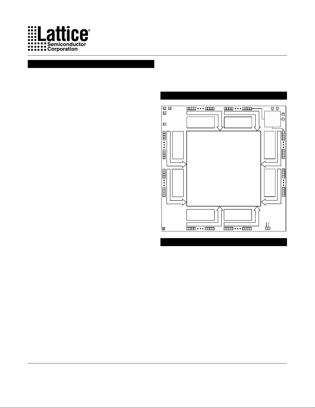
Functional Block Diagram
Generic
Input Bus
Generic
Input Bus
Logic Block
Logic Block
Logic Block
Logic Block
Input Bus
Generic
Global Routing Pool
(GRP)
Generic
Input Bus
Input Bus
Generic
Logic Block
Generic
Logic Block
Input Bus
Boundary
Scan
Interface
Logic Block
Generic
Input Bus
Logic Block
Generic
Input Bus
ispLSI 5000V Description
The ispLSI 5000V Family of In-System Programmable
High Density Logic Devices is based on Generic Logic
Blocks (GLBs) of 32 registered macrocells and a single
Global Routing Pool (GRP) structure interconnecting the
GLBs.
Outputs from the GLBs drive the Global Routing Pool
(GRP) between the GLBs. Switching resources are provided to allow signals in the Global Routing Pool to drive
any or all the GLBs in the device. This mechanism allows
fast, efficient connections across the entire device.
Each GLB contains 32 macrocells and a fully populated,
programmable AND-array with 160 logic product terms
and five extra control product terms. The GLB has 68
inputs from the Global Routing Pool which are available
Copyright © 2000 Lattice Semiconductor Corp. All brand or product names are trademarks or registered trademarks of their respective holders. The specifications and information herein are subject
to change without notice.
LATTICE SEMICONDUCTOR CORP., 5555 Northeast Moore Ct., Hillsboro, Oregon 97124, U.S.A. September 2000
Tel. (503) 268-8000; 1-800-LATTICE; FAX (503) 268-8556; http://www.latticesemi.com
15256va_04
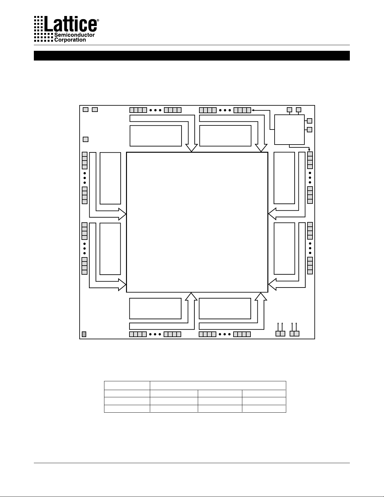
Specifications ispLSI 5256VA
Functional Block Diagram
Figure 1. ispLSI 5256VA Functional Block Diagram (272 BGA Option)
GOE0
GOE1
I/O 191
I/O 190
I/O 189
I/O 188
I/O 171
I/O 170
I/O 169
I/O 168
I/O 167
I/O 166
I/O 165
I/O 164
I/O 147
I/O 146
I/O 145
I/O 144
TCK
TMS
VCCIO
1
I/O 0 / TOE
I/O 1
I/O 2
I/O 3
I/O 20
I/O 21
I/O 22
I/O 23
I/O 24
I/O 25
I/O 26
I/O 27
I/O 44
I/O 45
I/O 46
I/O 47
Generic
Input Bus
Generic
Input Bus
Logic Block
Logic Block
Logic Block
Input Bus
Generic
Input Bus
Generic
Logic Block
Global Routing Pool
(GRP)
Boundary
Scan
Interface
Logic Block
Generic
Input Bus
Logic Block
Generic
Input Bus
TDI
TDO
I/O 143
I/O 142
I/O 141
I/O 140
I/O 123
I/O 122
I/O 121
I/O 120
I/O 119
I/O 118
I/O 117
I/O 116
I/O 99
I/O 98
I/O 97
I/O 96
GSET/GRST
Generic
Logic Block
Input Bus
I/O 48
I/O 49
I/O 50
I/O 51
I/O 68
I/O 69
I/O 70
I/O 71
Generic
Logic Block
Input Bus
I/O 72
I/O 73
I/O 74
I/O 75
I/O 92
I/O 93
I/O 94
I/O 95
CLK 1
CLK 0
CLK 3
CLK 2
1
1
1. CLK2, CLK3 and TOE signals are multiplexed with I/O signals. Which I/O is multiplexed is
determined by the package type used (see table below).
Package Type Multplexed Signals
208 PQFP I/O 89 / CLK2 I/O 98 / CLK3 I/O 0 / TOE
208 fpBGA I/O 89 / CLK2 I/O 98 / CLK3 I/O 0 / TOE
272 BGA I/O 119 / CLK2 I/O 131 / CLK3 I/O 0 / TOE
2
Specifications ispLSI 5256VA
ispLSI 5000V Description (Continued)
in both true and complement form for every product term.
The 160 product terms are grouped in 32 sets of five and
sent into a Product Term Sharing Array (PTSA) which
allows sharing up to a maximum of 35 product terms for
a single function. Alternatively, the PTSA can be bypassed for functions of five product terms or less. The
five extra product terms are used for shared GLB controls, set, reset, clock, clock enable and output enable.
The 32 registered macrocells in the GLB are driven by the
32 outputs from the PTSA or the PTSA bypass. Each
macrocell contains a programmable XOR gate, a programmable register/latch/toggle flip-flop and the
necessary clocks and control logic to allow combinatorial
or registered operation. The macrocells each have two
outputs, which can be fed back through the Global
Routing Pool. This dual output capability from the
macrocell allows efficient use of the hardware resources.
One output can be a registered function for example,
while the other output can be an unrelated combinatorial
function. A direct register input from the I/O pad facilitates efficient use of this feature to construct high-speed
input registers.
Macrocell registers can be clocked from one of several
global or product term clocks available on the device. A
global and product term clock enable is also provided,
eliminating the need to gate the clock to the macrocell
registers. Reset and preset for the macrocell register is
provided from both global and product term signals. The
macrocell register can be programmed to operate as a Dtype register, a D-type latch or a T-type flip flop.
The 32 outputs from the GLB can drive both the Global
Routing Pool and the device I/O cells. The Global
Routing Pool contains one line from each macrocell
output and one line from each I/O pin.
The input buffer threshold has programmable TTL/3.3V/
2.5V compatible levels. The output driver can source
4mA and sink 8mA in 3.3V mode. The output drivers
have a separate VCCIO reference input which is independent of the main VCC supply for the device. This
feature allows the output drivers to drive either 3.3V or
2.5V output levels while the device logic and the output
current drive is always powered from 3.3V. The output
drivers also provide individually programmable edge
rates and open drain capability. A programmable pullup
resistor is provided to tie off unused inputs and a programmable bus-hold latch is available to hold tristate
outputs in their last valid state until the bus is driven again
by some device.
The ispLSI 5000V Family features 3.3V, non-volatile insystem programmability for both the logic and the
interconnect structures, providing the means to develop
truly reconfigurable systems. Programming is achieved
through the industry standard IEEE 1149.1-compliant
Boundary Scan interface. Boundary Scan test is also
supported through the same interface.
An enhanced, multiple cell security scheme is provided
that prevents reading of the JEDEC programming file
when secured. After the device has been secured using
this mechanism, the only way to clear the security is to
execute a bulk-erase instruction.
ispLSI 5000V Family Members
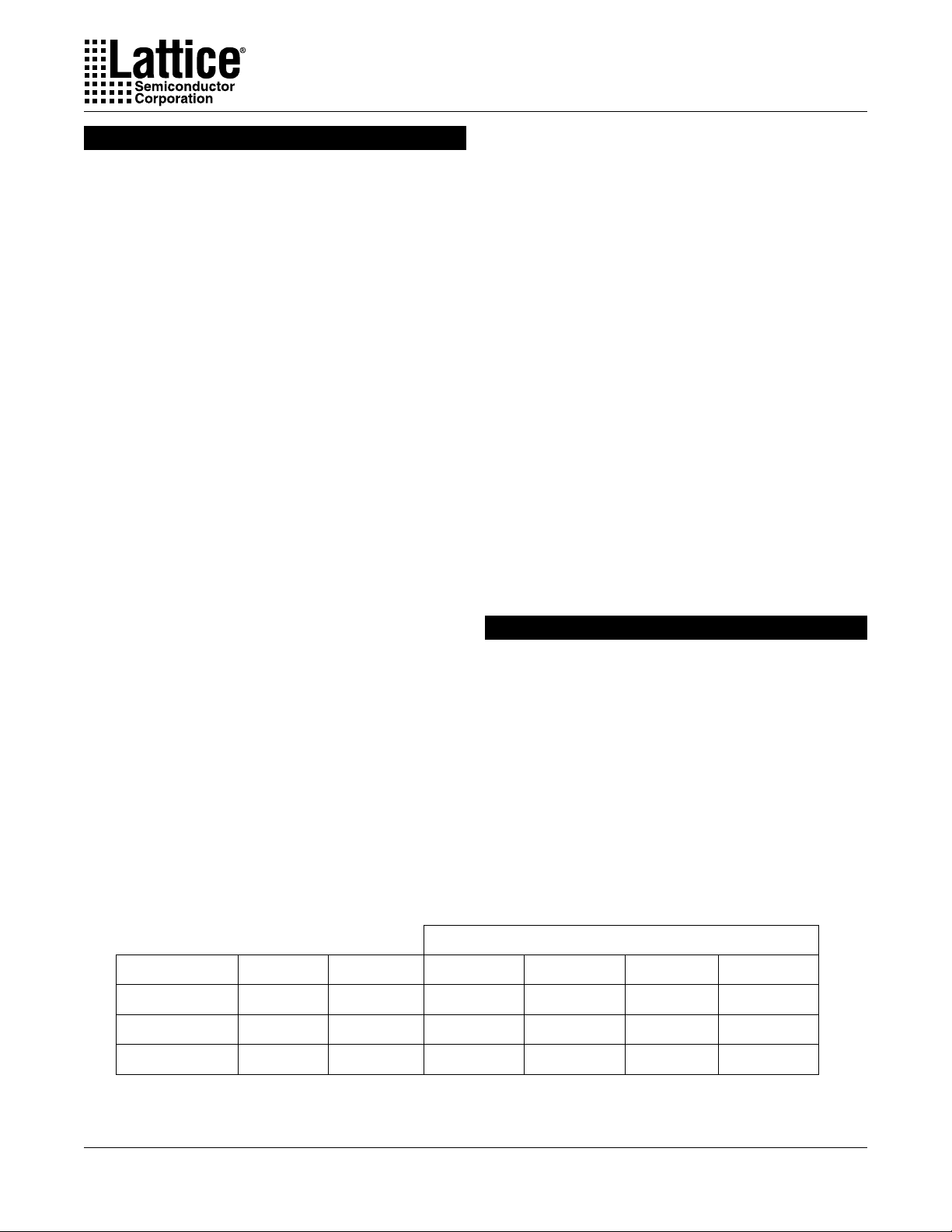
The ispLSI 5000V Family ranges from 256 macrocells to
512 macrocells and operates from a 3.3V power supply.
All family members will be available with multiple package options. The ispLSI 5000V Family device matrix
showing the various bondout options is shown in the table
below.
The interconnect structure (GRP) is very similar to Lattice's
existing ispLSI 1000, 2000 and 3000 families, but with an
enhanced interconnect structure for optimal pin locking
and logic routing. This eliminates the need for registered
I/O cells or an Output Routing Pool.
Table 1. ispLSI 5000V Family
eciveDsBLGsllecorcaMAGBpf802PFQP802AGB272AGB883
AV6525ISLpsi 8652O/I441O/I441O/I291—
AV4835ISLpsi 21483O/I441O/I441O/I291O/I882
AV2155ISLpsi 61215— O/I441O/I291O/I882
epyTegakcaP
3
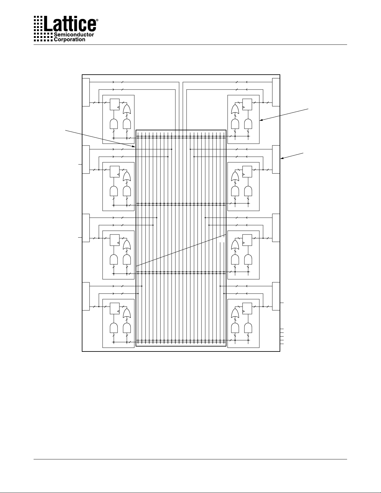
Figure 2. ispLSI 5256VA Block Diagram (192 I/O Version)
24 24
Global
Routing
Pool
(GRP)
24
I/O
24
32
32
DQ
32
160
160
5
PT
PT
5
160
68
Specifications ispLSI 5256VA
32
32
DQ
32
160
160
5
PT
PT
160
68
5
24
I/O
24
Generic
Logic
Block
(GLB)
CLK2
CLK3
24
24
I/O
24
24
I/O
24
24
I/O
24 24
32 32
32
DQ
32
160
160
5
PT
PT
5
160
68
24 24
32 32
32
DQ
32
160
5
160
PT
PT
5
160
68
24 24
32
32
DQ
32
160
160
5
PT
PT
5
160
68
24
32
DQ
160
160
PT
160
68
32
448
DQ
160
160
PT
160
68
32
32
DQ
160
160
PT
160
68
24
I/O
32
24
5
PT
5
24
I/O
32
24
5
PT
5
24
I/O
5512_384
TOE
CLK0
CLK1
GOE0
GOE1
SET/RESET
32
5
PT
5
Buffers/Pins
4
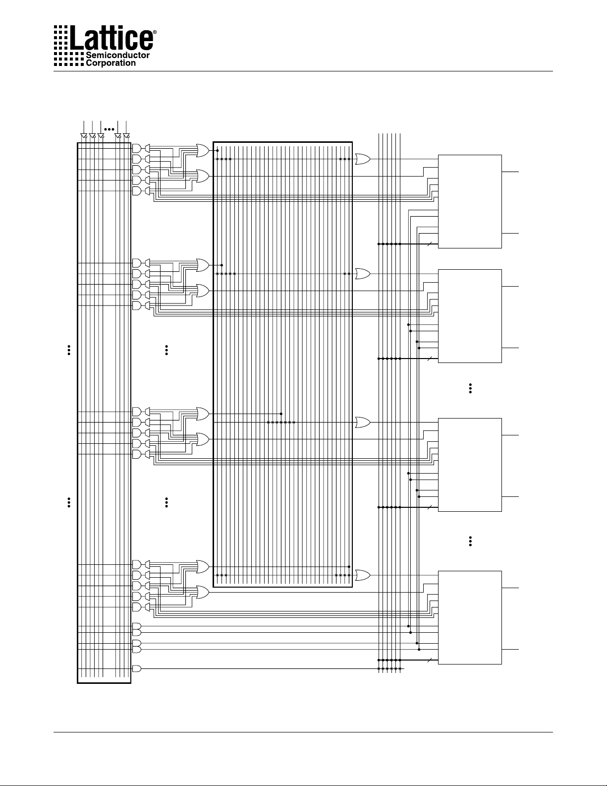
Figure 3. ispLSI 5000V Generic Logic Block (GLB)
From Global Routing Pool
0126667
PTSA
PT 0
PT 1
PT 2
PT 3
PT 4
PT 9
PT 8
PT 7
PT 6
PT 5
Specifications ispLSI 5256VA
Global PTOE Bus
Macrocell 0
From PTSA
PTSA bypass
PTOE
PT Clock
PT Reset
PT Preset
Shared PT Clock 0
Shared PT (P)reset 0
Shared PT Clock 1
Shared PT (P)reset 1
Global PTOE 0 ... 5
6
Macrocell 1
From PTSA
PTSA bypass
PTOE
PT Clock
PT Reset
PT Preset
Shared PT Clock 0
Shared PT (P)reset 0
Shared PT Clock 1
Shared PT (P)reset 1
Global PTOE 0 ... 5
6
To I/O Pad
To GRP
To I/O Pad
To GRP
PT 79
PT 78
PT 77
PT 76
PT 75
PT 159
PT 158
PT 157
PT 156
PT 155
PT 160
PT 161
PT 162
PT 163
PT 164
Programmable
AND Array
Macrocell 15
From PTSA
PTSA bypass
PTOE
PT Clock
PT Reset
PT Preset
Shared PT Clock 0
Shared PT (P)reset 0
Shared PT Clock 1
Shared PT (P)reset 1
Global PTOE 0 ... 5
6
Macrocell 31
From PTSA
PTSA bypass
PTOE
PT Clock
PT Reset
PT Preset
Shared PT Clock 0
Shared PT (P)reset 0
Shared PT Clock 1
Shared PT (P)reset 1
Global PTOE 0 ... 5
6
To I/O Pad
To GRP
To I/O Pad
To GRP
GLB_5K
5
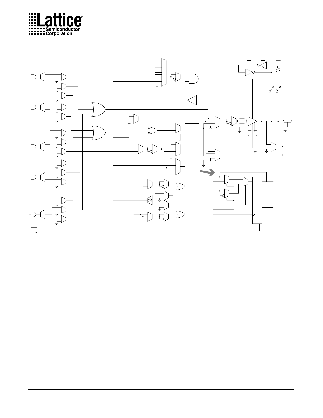
Figure 4. ispLSI 5000V Macrocell
Specifications ispLSI 5256VA
PTOE
PT Clock
PT Reset
PT Preset
GOE0
GOE1
TOE
Shared PT Clock 0
Shared PT Clock 1
CLK0
CLK1
CLK2
CLK3
SET/RESET
Shared PT (P)reset 0
Shared PT (P)reset 1
PTSA
Global PTOE 0
Global PTOE 1
Global PTOE 2
Global PTOE 3
Global PTOE 4
Global PTOE 5
PTSA bypass
DQ
D/T
Clk En
R/L
Clk
RP
D/T
Clk En
Clk
Delay
Slew
rate
2.5V/3.3V
Output
Open
drain
DQD
VCCIOVCCIO VCC
To GRP
Q
Register/
Latch
I/O Pad
Programmable
Speed/Power
Option
RP
6
Specifications ispLSI 5256VA
Global Clock Distribution
The ispLSI 5000V Family has four dedicated clock input
pins: CLK0 - CLK3. CLK0 input is used as the dedicated
master clock that has the lowest internal clock skew with
no clock inversion to maintain the fastest internal clock
Figure 5. ispLSI 5000V Global Clock Structure
CLK 0
CLK 1
IO/CLK 2
IO/CLK 3
speed. The clock inversion is available on the remaining
CLK1 - CLK3 signals. By sharing the pins with the I/O
pins, CLK2 and CLK3 can not only be inverted but also is
available for logic implementation through GRP signal
routing. Figure 5 shows these different clock distribution
options.
CLK0
CLK1
To GRP
CLK2
CLK3
To GRP
GSET/GRST
SET/RESET
7
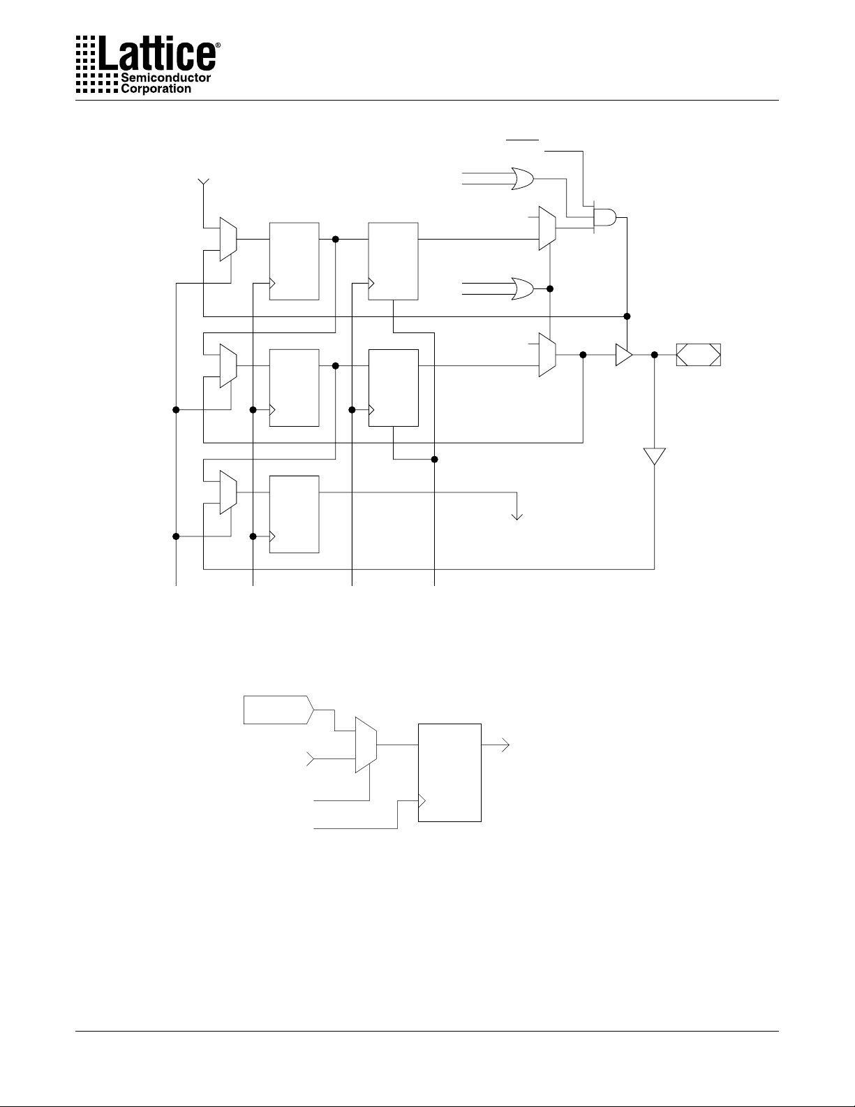
Figure 6. Boundary Scan Register Circuit for I/O Pins
Specifications ispLSI 5256VA
HIGHZ
EXTEST
SCANIN
(from previous
cell)
Shift DR
Clock DR
BSCAN
Registers
DQ DQ
DQ
DQ
Update DR
BSCAN
Latches
DQ
Reset
TOE
Normal
Function
EXTEST
PROG_MODE
Normal
Function
OE
SCANOUT
(to next cell)
0
1
0
1
I/O Pin
Figure 7. Boundary Scan Register Circuit for Input-Only Pins
Input Pin
SCANIN
DQ
(from previous
cell)
Shift DR
Clock DR
8
SCANOUT
(to next cell)