


Lattice Semiconductor Corporation ISPLSI1048EA-170LT128, ISPLSI1048EA-170LQ128, ISPLSI1048EA-125LT128, ISPLSI1048EA-125LQ128, ISPLSI1048EA-100LT128 Datasheet
...
ispLSI® 1048EA
In-System Programmable High Density PLD
Functional Block DiagramFeatures
• HIGH DENSITY PROGRAMMABLE LOGIC
— 8,000 PLD Gates
— 96 I/O Pins, Eight Dedicated Inputs
— 288 Registers
— High-Speed Global Interconnects
— Wide Input Gating for Fast Counters, State
Machines, Address Decoders, etc.
— Small Logic Block Size for Random Logic
— Functionally Compatible with ispLSI 1048C and 1048E
• NEW FEATURES
— 100% IEEE 1149.1 Boundary Scan Testable
— ispJTAG™ In-System Programmable Via IEEE 1149.1
(JTAG) Test Access Port
— User Selectable 3.3V or 5V I/O supports Mixed
Voltage Systems (V
CCIO Pin)
— Open Drain Output Option
2
• HIGH PERFORMANCE E
fmax = 170 MHz Maximum Operating Frequency
—
—
tpd = 5.0 ns Propagation Delay
CMOS® TECHNOLOGY
— TTL Compatible Inputs and Outputs
— Electrically Eraseable and Reprogrammable
— Non-Volatile
— 100% Tested at Time of Manufacture
• IN-SYSTEM PROGRAMMABLE
— Increased Manufacturing Yields, Reduced Time-to-
Market and Improved Product Quality
— Reprogram Soldered Devices for Faster Prototyping
• OFFERS THE EASE OF USE AND FAST SYSTEM
SPEED OF PLDs WITH THE DENSITY AND FLEXIBILITY
OF FIELD PROGRAMMABLE GATE ARRAYS
— Complete Programmable Device Can Combine Glue
Logic and Structured Designs
— Enhanced Pin Locking Capability
— Four Dedicated Clock Input Pins
— Synchronous and Asynchronous Clocks
— Programmable Output Slew Rate Control to
Minimize Switching Noise
— Flexible Pin Placement
— Optimized Global Routing Pool Provides Global
Interconnectivity
• ispDesignEXPERT™ – LOGIC COMPILER AND COMPLETE ISP DEVICE DESIGN SYSTEMS FROM HDL
SYNTHESIS THROUGH IN-SYSTEM PROGRAMMING
— Superior Quality of Results
— Tightly Integrated with Leading CAE Vendor Tools
— Productivity Enhancing Timing Analyzer, Explore
Tools, Timing Simulator and ispANALYZER™
— PC and UNIX Platforms
Output Routing Pool
F7 F6 F5 F4 F3 F2 F1 F0
A0
A1
A2
A3
Global Routing Pool (GRP) GLB
A4
A5
Output Routing Pool
A6
A7
B0 B1 B2 B3 B4 B5 B6 B7
Output Routing Pool
Output Routing Pool
E7 E6 E5 E4 E3 E2 E1 E0
DQ
DQ
Logic
Array
DQ
DQ
C0 C1 C2 C3 C4 C5 C6 C7
Output Routing Pool
D7
D6
D5
D4
D3
D2
Output Routing Pool
D1
D0
CLK
0139A/1048EA
Description
The ispLSI 1048EA is a High Density Programmable
Logic Device containing 288 Registers, 96 Universal I/O
pins, eight Dedicated Input pins, four Dedicated Clock
Input pins, two dedicated Global OE input pins, and a
Global Routing Pool (GRP). The GRP provides complete
interconnectivity between all of these elements. The
ispLSI 1048EA features 5V in-system programmability
and in-system diagnostic capabilities via IEEE 1149.1
Test Access Port. The ispLSI 1048EA offers non-volatile
reprogrammability of the logic, as well as the interconnect to provide truly reconfigurable systems. A functional
superset of the ispLSI 1048 architecture, the ispLSI
1048EA device adds user selectable 3.3V or 5V I/O and
open-drain output options.
The basic unit of logic on the ispLSI 1048EA device is the
Generic Logic Block (GLB). The GLBs are labeled A0,
A1…F7 (see Figure 1). There are a total of 48 GLBs in the
ispLSI 1048EA device. Each GLB has 18 inputs, a
programmable AND/OR/Exclusive OR array, and four
outputs which can be configured to be either combinatorial or registered. Inputs to the GLB come from the GRP
and dedicated inputs. All of the GLB outputs are brought
back into the GRP so that they can be connected to the
inputs of any other GLB on the device.
Copyright © 2000 Lattice Semiconductor Corp. All brand or product names are trademarks or registered trademarks of their respective holders. The specifications and information herein are subject
to change without notice.
LATTICE SEMICONDUCTOR CORP., 5555 Northeast Moore Ct., Hillsboro, Oregon 97124, U.S.A. June 2000
Tel. (503) 268-8000; 1-800-LATTICE; FAX (503) 268-8556; http://www.latticesemi.com
1048ea_03 1
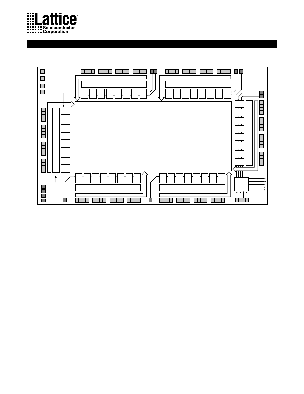
Functional Block Diagram
Figure 1. ispLSI 1048EA Functional Block Diagram
I/O94I/O95I/O93I/O92I/O91I/O90I/O89I/O88I/O87I/O86I/O85I/O84I/O83I/O82I/O81I/O
RESET
GOE 0
GOE 1
VCCIO
I/O 0
I/O 1
I/O 2
I/O 3
I/O 4
I/O 5
I/O 6
I/O 7
I/O 8
I/O 9
I/O 10
I/O 11
I/O 12
I/O 13
I/O 14
I/O 15
TDO
TMS
TCK
Generic
Logic Blocks
(GLBs)
A0
A1
A2
A3
A4
Input Bus
A5
Output Routing Pool (ORP)
A6
A7
TDI
Megablock
IN 2
F7 F6 F5 F4 F3 F2 F1 F0
B0 B1 B2 B3 B4 B5 B6 B7
Output Routing Pool (ORP)
I/O17I/O16I/O18I/O19I/O20I/O21I/O22I/O23I/O24I/O25I/O26I/O27I/O28I/O29I/O30I/O
Input Bus
Output Routing Pool (ORP)
Input Bus
31
Specifications ispLSI 1048EA
IN
IN
11
10
80
Global
Routing
Pool
(GRP)
IN
4
I/O78I/O79I/O77I/O76I/O75I/O74I/O73I/O72I/O71I/O70I/O69I/O68I/O67I/O66I/O65I/O
Input Bus
Output Routing Pool (ORP)
E7 E6 E5 E4 E3 E2 E1 E0
C0 C1 C2 C3 C4 C5 C6 C7
Output Routing Pool (ORP)
Input Bus
I/O33I/O32I/O34I/O35I/O36I/O37I/O38I/O39I/O40I/O41I/O42I/O43I/O44I/O45I/O46I/O
IN
IN
9
64
8
D7
D6
D5
D4
D3
D2
D1
D0
Clock
Distribution
Network
47
Y0Y1Y2Y
IN 7
IN 6
I/O 63
I/O 62
I/O 61
I/O 60
I/O 59
I/O 58
I/O 57
I/O 56
I/O 55
lnput Bus
I/O 54
I/O 53
Output Routing Pool (ORP)
CLK 0
CLK 1
CLK 2
IOCLK 0
IOCLK 1
3
0139F/1048EA
I/O 52
I/O 51
I/O 50
I/O 49
I/O 48
The device also has 96 I/O cells, each of which is directly
connected to an I/O pin. Each I/O cell can be individually
programmed to be a combinatorial input, registered
input, latched input, output or bi-directional
I/O pin with 3-state control. The signal levels are TTL
compatible voltages and the output drivers can source
2mA or sink 8mA. Each output can be programmed
independently for fast or slow output slew rate to
minimize overall output switching noise. By connecting
the VCCIO pin to a common 5V or 3.3V power supply,
I/O output levels can be matched to 5V or 3.3V compatible voltages.
Eight GLBs, 16 I/O cells, dedicated inputs (if available)
and one ORP are connected together to make a
Megablock (Figure 1). The outputs of the eight GLBs are
connected to a set of 16 universal I/O cells by the ORP.
Each ispLSI 1048EA device contains six Megablocks.
The GRP has, as its inputs, the outputs from all of the
GLBs and all of the inputs from the bi-directional I/O cells.
All of these signals are made available to the inputs of the
GLBs. Delays through the GRP have been equalized to
minimize timing skew.
Clocks in the ispLSI 1048EA device are selected using
the Clock Distribution Network. Four dedicated clock pins
(Y0, Y1, Y2 and Y3) are brought into the distribution
network, and five clock outputs (CLK 0, CLK 1, CLK 2,
IOCLK 0 and IOCLK 1) are provided to route clocks to the
GLBs and I/O cells. The Clock Distribution Network can
also be driven from a special clock GLB (D0). The logic
of this GLB allows the user to create an internal clock
from a combination of internal signals within the device.
Programmable Open-Drain Outputs
In addition to the standard output configuration, the
outputs of the ispLSI 1048EA are individually programmable, either as a standard totem-pole output or an
open-drain output. The totem-pole output drives the
specified Voh and Vol levels, whereas the open-drain
output drives only the specified Vol. The Voh level on the
open-drain output depends on the external loading and
pull-up. This output configuration is controlled by a programmable fuse. The default configuration when the
device is in bulk erased state is totem-pole configuration.
The open-drain/totem-pole option is selectable through
the ispDesignEXPERT software tools.
2
Specifications ispLSI 1048EA
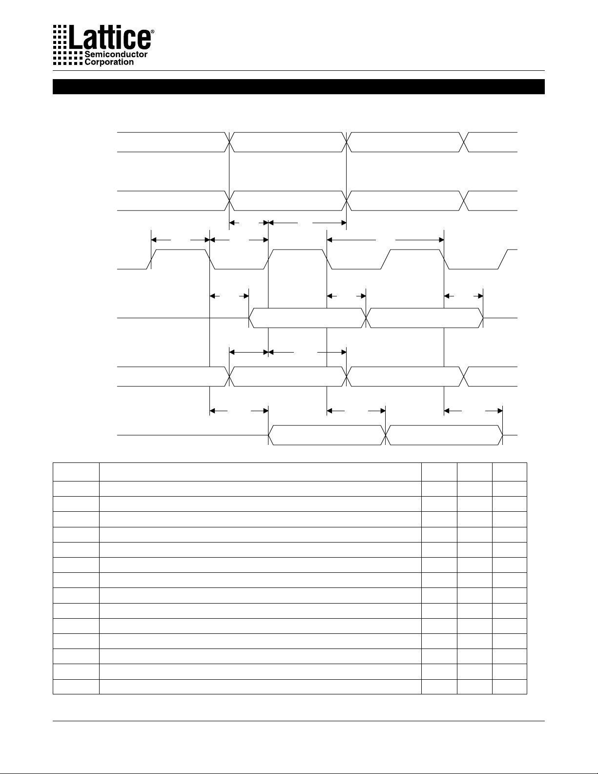
Boundary Scan
Figure 2. Boundary Scan Waveforms and Timing Specifications
TMS
TDI
TCK
TDO
Data to be
captured
Data to be
driven out
T
btch
T
T
btvo
T
T
btcl
T
btcpsu
btuov
btsu
Data Captured
T
bth
T
btcp
T
btco
Valid Data Valid Data
T
btcph
T
btuco
Valid Data Valid Data
T
btoz
T
btuoz
Symbol Parameter Min Max Units
t
btcp
t
btch
t
btcl
t
btsu
t
bth
t
rf
t
btco
t
btoz
t
btvo
t
btcpsu
t
btcph
t
btuco
t
btuoz
t
btuov
TCK [BSCAN test] clock pulse width 100 – ns
TCK [BSCAN test] pulse width high 50 – ns
TCK [BSCAN test] pulse width low 50 – ns
TCK [BSCAN test] setup time 20 – ns
TCK [BSCAN test] hold time 25 – ns
TCK [BSCAN test] rise and fall time 50 – mV/ns
TAP controller falling edge of clock to valid output – 25 ns
TAP controller falling edge of clock to data output disable – 25 ns
TAP controller falling edge of clock to data output enable – 25 ns
BSCAN test Capture register setup time 40 – ns
BSCAN test Capture register hold time 25 – ns
BSCAN test Update reg, falling edge of clock to valid output – 50 ns
BSCAN test Update reg, falling edge of clock to output disable – 50 ns
BSCAN test Update reg, falling edge of clock to output enable – 50 ns
3
Specifications ispLSI 1048EA
Absolute Maximum Ratings
1
Supply Voltage Vcc. ................................. -0.5 to +7.0V
Input Voltage Applied........................-2.5 to VCC +1.0V
Off-State Output Voltage Applied .....-2.5 to VCC +1.0V
Storage Temperature................................ -65 to 150°C
Case Temp. with Power Applied .............. -55 to 125°C
Max. Junction Temp. (TJ) with Power Applied ... 150°C
1. Stresses above those listed under the “Absolute Maximum Ratings” may cause permanent damage to the device. Functional
operation of the device at these or at any other conditions above those indicated in the operational sections of this specification
is not implied (while programming, follow the programming specifications).
DC Recommended Operating Conditions
MIN. MAX. UNITS
4.75
4.75
3.0
0
2.0
5.25
5.25
3.6
0.8
+1
V
cc
Table 2-0005/1048EA
V
V
V
V
V
V
V
V
V
CC
CCIO
IL
IH
SYMBOL
PARAMETER
Supply Voltage
Supply Voltage: Output Drivers
Input Low Voltage
Input High Voltage
Commercial
5V
3.3V
TA = 0°C to + 70°C
Capacitance (TA=25oC, f=1.0 MHz)
SYMBOL
C
1
C
2
Dedicated Input, I/O, Y1, Y2, Y3, Clock Capacitance
Y0 Clock Capacitance
PARAMETER
Erase/Reprogram Specifications
PARAMETER MINIMUM MAXIMUM UNITS
Erase/Reprogram Cycles
UNITSTYPICAL TEST CONDITIONS
8
10
10000 – Cycles
pf
pf
V = 5.0V, V = 2.0V
CC
V = 5.0V, V = 2.0V
CC PIN
PIN
Table 2-0006/1048EA
Table 2-0008/1048EA
4
Switching Test Conditions
Specifications ispLSI 1048EA
Input Pulse Levels
Input Rise and Fall Time 10% to 90%
Input Timing Reference Levels
Output Timing Reference Levels
Output Load
3-state levels are measured 0.5V from
steady-state active level.
GND to 3.0V
1.5ns
1.5V
1.5V
See Figure 3
Table 2-0003/1048EA
Output Load Conditions (see Figure 3)
TEST CONDITION R1 R2 CL
A 470Ω 390Ω 35pF
Active High
B
Active Low
Active High to Z
at V -0.5V
C
Active Low to Z
at V +0.5V
OH
OL
∞ 390Ω 35pF
470Ω 390Ω 35pF
∞ 390Ω 5pF
470Ω 390Ω 5pF
DC Electrical Characteristics
Over Recommended Operating Conditions
Table 2-0004a
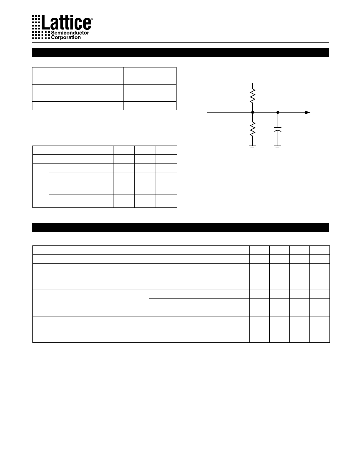
Figure 3. Test Load
+ 5V
R
1
Device
Output
R
2
*
CL includes Test Fixture and Probe Capacitance.
C
*
L
Test
Point
0213a
SYMBOL
V
OL
V
OH
I
IL
I
IH
I
IL-PU
1
I
OS
2, 4, 5
I
CC
Output Low Voltage
Output High Voltage
Input or I/O Low Leakage Current
Input or I/O High Leakage Current
I/O Active Pull-Up Current
Output Short Circuit Current V
Operating Power Supply Current
PARAMETER
I
= 8 mA
OL
I
= -2 mA, V
OH
I
= -4 mA, V
OH
0V ≤ V
IN
- 0.2)V ≤ VIN ≤ V
(V
CCIO
≤ V
V
CCIO
0V ≤ V
IN
= 5.0V or 3.3V, V
CCIO
V
= 0.0V, VIH = 3.0V
IL
f
TOGGLE
1. One output at a time for a maximum duration of one second. V
CONDITION MIN. TYP.3MAX. UNITS
= 3.0V
CCIO
= 4.75V
CCIO
≤ VIL (Max.)
≤ 5.25V
IN
≤ V
IL
—
2.4
2.4 ——V
—
CCIO
—
—
—
= 0.5V ——-240 mA
OUT
—
—
—
—
—
—
— 190 mA—
= 1 MHz
= 0.5V was selected to avoid test
OUT
0.4
—
-10
10
10
-200
Table 2-0007/1048EA
problems by tester ground degradation. Characterized but not 100% tested.
2. Meaured using eight 16-bit counters.
3. Typical values are at V
= 5V and TA = 25°C.
CC
4. Unused inputs held at 0.0V.
5. Maximum I
varies widely with specific device configuration and operating frequency. Refer to the
CC
Power Consumption section of this data sheet and the Thermal Management section of the Lattice Semiconductor
Data Book CD-ROM to estimate maximum I
CC
.
V
V
µA
µA
µA
µA
5