Lattice Semiconductor Corporation GAL20VP8B-25LP, GAL20VP8B-15LP, GAL20VP8B-15LJ Datasheet

GAL20VP8
High-Speed E2CMOS PLD
Generic Array Logic™
Features
• HIGH DRIVE E2CMOS® GAL® DEVICE
— TTL Compatible 64 mA Output Drive
— 15 ns Maximum Propagation Delay
— Fmax = 80 MHz
— 10 ns Maximum from Clock Input to Data Output
— UltraMOS
• ENHANCED INPUT AND OUTPUT FEATURES
— Schmitt Trigger Inputs
— Programmable Open-Drain or Totem-Pole Outputs
— Active Pull-Ups on All Inputs and I/O pins
2
CELL TECHNOLOGY
•E
— Reconfigurable Logic
— Reprogrammable Cells
— 100% Tested/100% Y ields
— High Speed Electrical Erasure (<100ms)
— 20 Year Data Retention
• EIGHT OUTPUT LOGIC MACROCELLS
— Maximum Flexibility for Complex Logic Designs
— Programmable Output Polarity
— Architecturally Compatible with Standard GAL20V8
• PRELOAD AND POWER-ON RESET OF ALL REGISTERS
— 100% Functional Testability
• APPLICATIONS INCLUDE:
— Ideal for Bus Control & Bus Arbitration Logic
— Bus Address Decode Logic
— Memory Address, Data and Control Circuits
— DMA Control
• ELECTRONIC SIGNA TURE FOR IDENTIFICATION
®
Advanced CMOS Technology
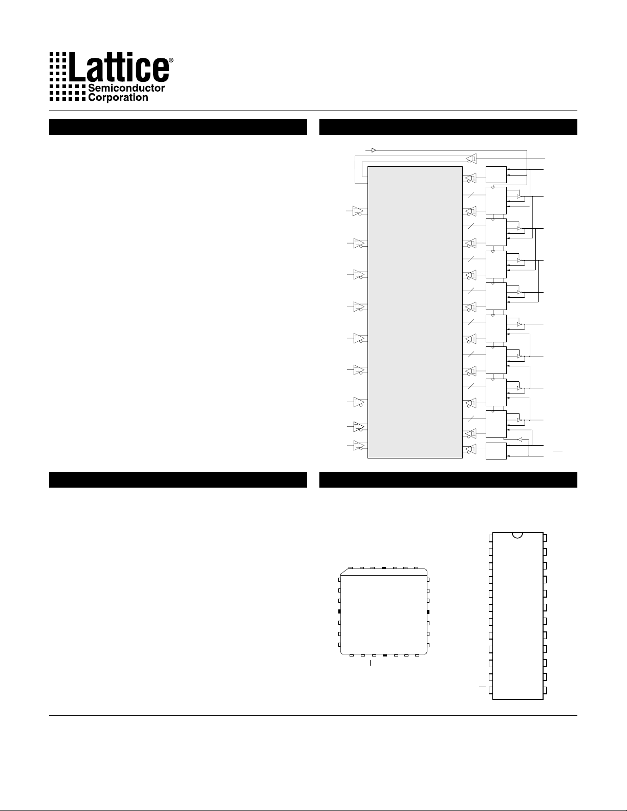
Functional Block Diagram
I/CLK
I
I
I
I
(64 X 40)
I
AND-ARRAY
PROGRAMMABLE
I
I
I
I
I
I
IMUX
CLK
8
OLMC
8
OLMC
8
OLMC
8
OLMC
8
OLMC
8
OLMC
8
OLMC
8
OLMC
OE
IMUX
I
I/O/Q
I/O/Q
I/O/Q
I/O/Q
I/O/Q
I/O/Q
I/O/Q
I/O/Q
I
I/OE
Description
Pin Configuration
The GAL20VP8, with 64 mA drive capability and 15 ns maximum
propagation delay time is ideal for Bus and Memory control applications. The GAL20VP8 is manufactured using Lattice
Semiconductor's advanced E2CMOS process which combines
CMOS with Electrically Erasable (E
2
) floating gate technology. High
speed erase times (<100ms) allow the devices to be reprogrammed
quickly and efficiently .
System bus and memory interfaces require control logic before
driving the bus or memory interface signals. The GAL20VP8
combines the familiar GAL20V8 architecture with bus drivers as
its outputs. The generic architecture provides maximum design flexibility by allowing the Output Logic Macrocell (OLMC) to be configured by the user. The 64mA output drive eliminates the need for
additional devices to provide bus-driving capability.
Unique test circuitry and reprogrammable cells allow complete AC,
DC, and functional testing during manufacture. As a result,
Lattice Semiconductor delivers 100% field programmability and
functionality of all GAL products. In addition, 100 erase/write cycles
I/CLK
I
426
5
I
I
Vcc
7
NC
I
9
I
I
11
12 14 16 18
I
NC
I
228
GAL20VP8
T op View
I
NC
I/OE
I/O/Q
I
I
25
23
21
19
I
I/O/Q
I/O/Q
I/O/Q
I/O/Q
I/O/Q
NC
GND
I/O/Q
I/O/Q
I/CLK
Vcc
I/OE
I
I
I
I
I
I
I
I
I
DIPPLCC
1
GAL
20VP8
6
12
I
24
I
I/O/Q
I/O/Q
I/O/Q
I/O/Q
GND
18
I/O/Q
I/O/Q
I/O/Q
I/O/Q
I
13
and data retention in excess of 20 years are specified.
Copyright © 1997 Lattice Semiconductor Corp. All brand or product names are trademarks or registered trademarks of their respective holders. The specifications and information herein are subject
to change without notice.
LATTICE SEMICONDUCTOR CORP., 5555 Northeast Moore Ct., Hillsboro, Oregon 97124, U.S.A. December 1997
Tel. (503) 268-8000; 1-800-LATTICE; FAX (503) 268-8556; http://www.latticesemi.com
20vp8_03
1

Specifications GAL20VP8
GAL20VP8 Ordering Information
Commercial Grade Specifications
Tpd (ns) Tsu (ns) Tco (ns) Icc (mA) Ordering # Package
15 8 10 115 GAL20VP8B-15LP 24-Pin Plastic DIP
115 GAL20VP8B-15LJ 28-Lead PLCC
25 10 15 115 GAL20VP8B-25LP 24-Pin Plastic DIP
115 GAL20VP8B-25LJ 28-Lead PLCC
Part Number Description
GAL20VP8B
Device Name
Speed (ns)
PowerL = Low Power
XXXXXXXX XX X X X
_
Grade
Package
Blank = Commercial
P = Plastic DIP
J = PLCC
2

Output Logic Macrocell (OLMC)
Specifications GAL20VP8
The following discussion pertains to configuring the output logic
macrocell. It should be noted that actual implementation is accomplished by development software/hardware and is completely transparent to the user.
There are three global OLMC configuration modes possible:
simple, complex, and registered. Details of each of these modes
is illustrated in the following pages. T wo global bits, SYN and AC0,
control the mode configuration for all macrocells. The XOR bit of
Compiler Support for OLMC
Software compilers support the three different global OLMC modes
as different device types. Most compilers also have the ability to
automatically select the device type, generally based on the register
usage and output enable (OE) usage. Register usage on the device
forces the software to choose the registered mode. All combinatorial outputs with OE controlled by the product term will force the
software to choose the complex mode. The software will choose
the simple mode only when all outputs are dedicated combinatorial
without OE control. For further details, refer to the compiler software manuals.
When using compiler software to configure the device, the user
must pay special attention to the following restrictions in each mode.
In registered mode pin 1(2) and pin 12(14) are permanently con-
figured as clock and output enable, respectively. These pins cannot
be configured as dedicated inputs in the registered mode.
each macrocell controls the polarity of the output in any of the three
modes, while the AC1 and AC2 bit of each of the macrocells controls
the input/output and totem-pole/open-drain configuration. These
two global and 24 individual architecture bits define all possible configurations in a GAL20VP8. The information given on these architecture bits is only to give a better understanding of the device.
Compiler software will transparently set these architecture bits from
the pin definitions, so the user should not need to directly manipulate
these architecture bits.
In complex mode pin 1(2) and pin 12(14) become dedicated in-
puts and use the feedback paths of pin 22(26) and pin 14(17) respectively . Because of this feedback path usage, pin 22(26) and
pin 14(17) do not have the feedback option in this mode.
In simple mode all feedback paths of the output pins are routed
via the adjacent pins. In doing so, the two inner most pins (pins
17(20) and 19(23)) will not have the feedback option as these pins
are always configured as dedicated combinatorial output.
In addition to the architecture configurations, the logic compiler
software also supports configuration of either totem-pole or opendrain outputs. The actual architecture bit configuration, again, is
transparent to the user with the default configuration being the
standard totem-pole output.
3

Registered Mode
Specifications GAL20VP8
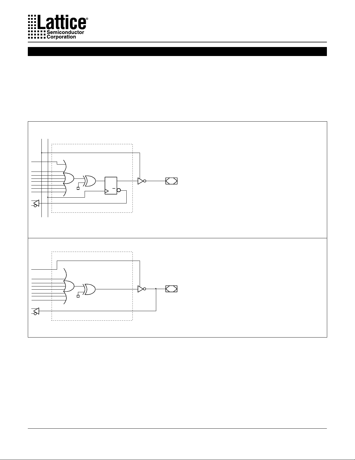
In the Registered mode, macrocells are configured as dedicated
registered outputs or as I/O functions.
All registered macrocells share common clock and output enable
control pins. Any macrocell can be configured as registered or I/
O. Up to eight registers or up to eight I/Os are possible in this mode.
Dedicated input or output functions can be implemented as subsets of the I/O function.
CLK
DQ
XOR
OE
Q
Registered outputs have eight product terms per output. I/Os have
seven product terms per output.
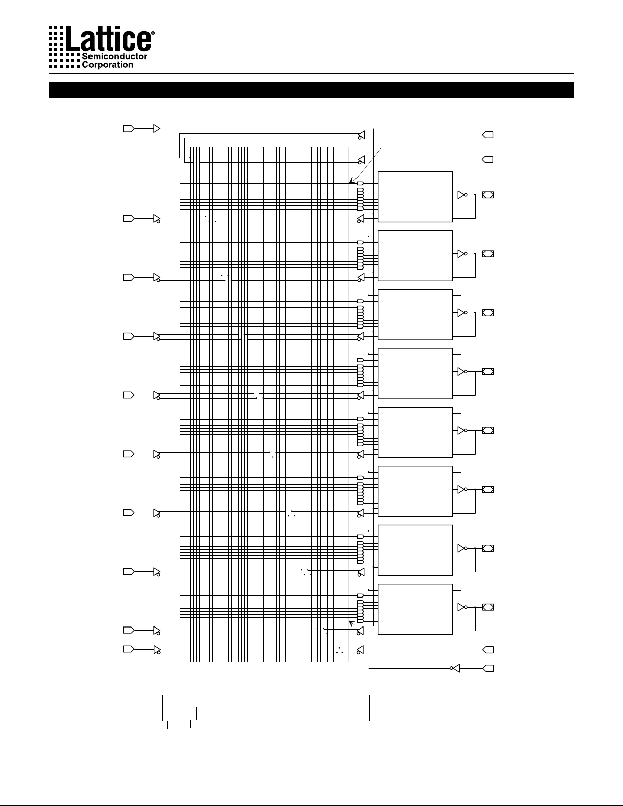
The JEDEC fuse numbers, including the User Electronic Signature
(UES) fuses and the Product T erm Disable (PTD) fuses, are shown
on the logic diagram on the following page.
Registered Configuration for Registered Mode
- SYN=0.
- AC0=1.
- XOR=0 defines Active Low Output.
- XOR=1 defines Active High Output.
- AC1=0 defines this output configuration.
- AC2=1 defines totem pole output.
- AC2=0 defines open-drain output.
- Pin 1(2) controls common CLK for the registered
outputs.
- Pin 12(14) controls common OE for the registered
outputs.
- Pin 1(2) & Pin 12(14) are permanently configured as
CLK & OE for registered output configuration.
Combinatorial Configuration for Registered Mode
- SYN=0.
- AC0=1.
- XOR=0 defines Active Low Output.
- XOR=1 defines Active High Output.
- AC1=1 defines this output configuration.
XOR
Note: The development software configures all of the architecture control bits and checks for proper pin usage automatically.
- AC2=1 defines totem pole output.
- AC2=0 defines open-drain output.
- Pin 1(2) & Pin 12(14) are permanently configured as
CLK & OE. for registered output configuration.
4

Registered Mode Logic Diagram
1(2)
Specifications GAL20VP8
DIP (PLCC) Package Pinouts
2824 3632201612840
PTD
2640
24(28)
23(27)
2(3)
3(4)
4(5)
5(6)
7(9)
0000
0280
0320
0600
0640
0920
0960
1240
1280
1560
OLMC
XOR-2560
AC1-2632
AC2-2706
OLMC
XOR-2561
AC1-2633
AC2-2707
OLMC
XOR-2562
AC1-2634
AC2-2708
OLMC
XOR-2563
AC1-2635
AC2-2709
OLMC
XOR-2564
AC1-2636
AC2-2710
22(26)
21(25)
20(24)
19(23)
17(20)
8(10)
9(11)
10(12)
11(13)
1600
1880
1920
2200
2240
2520
64-USER ELECTRONIC SIGNATURE FUSES
2568, 2569, .... .... 2630, 2631
Byte7 Byte6 .... .... Byte1 Byte0
MSB LSB
OLMC
XOR-2565
AC1-2637
AC2-2711
16(19)
OLMC
XOR-2566
AC1-2638
AC2-2712
15(18)
OLMC
OE
14(17)
13(16)
12(14)
XOR-2567
AC1-2639
AC2-2713
2703
SYN-2704
AC0-2705
5

Complex Mode
Specifications GAL20VP8
In the Complex mode, macrocells are configured as output only or
I/O functions.
Up to six I/Os are possible in this mode. Dedicated inputs or outputs
can be implemented as subsets of the I/O function. The two outer
most macrocells (pins 14(17) & 22(26)) do not have input capability .
Designs requiring eight I/Os can be implemented in the Registered
mode.
XOR
All macrocells have seven product terms per output. One product
term is used for programmable output enable control. Pins 1(2) and
12(14) are always available as data inputs into the AND array.
The JEDEC fuse numbers including the UES fuses and PTD fuses
are shown on the logic diagram on the following page.
Combinatorial I/O Configuration for Complex Mode
- SYN=1.
- AC0=1.
- XOR=0 defines Active Low Output.
- XOR=1 defines Active High Output.
- AC1 has no effect on this mode.
- AC2=1 defines totem pole output.
- AC2=0 defines open-drain output.
- Pin 15(18) through Pin 21(25) are configured to this
function.
Combinatorial Output Configuration for Complex Mode
- SYN=1.
- AC0=1.
- XOR=0 defines Active Low Output.
XOR
Note: The development software configures all of the architecture control bits and checks for proper pin usage automatically.
- XOR=1 defines Active High Output.
- AC1 has no effect on this mode.
- AC2=1 defines totem pole output.
- AC2=0 defines open-drain output.
- Pin 14(17) and Pin 22(26) are configured to this
function.
6
 Loading...