

Page 1

Evaluating the ORCA ORSO42G5 with the
High-Speed SERDES Board
April 2004 Technical Note TN1070
Introduction
Contained in this package is information that will assist you in evaluating and verifying your ORCA® ORSO42G5
designs using the Lattice High-Speed SERDES Board and the ORCAstra system bus control panel (available for
download from the Lattice web site at www.latticesemi.com/products/devtools/software/orcastra/index.cfm).
The Lattice High-Speed SERDES Board supports a number of testing and evaluation setups for both the
ORT42G5 and the ORSO42G5. This document will cover some common types of evaluation testing that can be
performed on the ORSO42G5 device in SERDES-only and SONET modes. The tests include transmitter eye diagram measurement, SONET Near-end Loop-back and SERDES-only, SONET and Aligned SONET Far-end Loopback. All of the described evaluation setups use the orso4_felb6.bit bitstream. This bitstream is included with the
package you have downloaded from the Lattice web site at www.latticesemi.com/products/devtools/hardware/orso42g5-board/index.cfm. A unique ORCAstra macro is used to configure the device for each test.
PC and Evaluation Board Setup
This document assumes the ORCAstra application and bitstream programming software (ispVM®) are installed on
the user’s PC. It also assumes the baseline board configuration listed below. (The user is also encouraged to
experiment with other configurations.)
• All jumpers should be in their default position and default programming in the ispPAC®-POWR1208 as
described in the Evaluation Board User Manual. This will apply power in the recommended sequence and
provide 3.3V V
• ispDOWNLOAD® cable (pDS4102-DL2) connected to the parallel port of the PC and to the ispVM connector on the board (J30). The pDS4102-DL2 is included with the Lattice High-Speed SERDES Board. Alternately, a HW-USB-1A ispDOWNLOAD cable can be used.)
• ORCAstra connected to the parallel or USB port on the PC and the ORCAstra Interface DB-25 or USB connector on the board (J108).
• External differential clock connected to the External System Clock SMA connectors (J87/J88 and J84/J85).
• External power should be provided from the Molex cable and power module.
to all banks.
DDIO
Recommended Reading
• ORSO42G5 Data Sheet
• ORCA Series 4 FPGA Data Sheet
• ispVM System Software Data Sheet
• ispDOWNLOAD Cable Data Sheet
• High-Speed SERDES Briefcase Board User Manual
• ORCAstra System Bus Control Panel User Manual
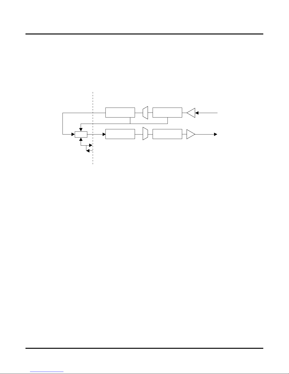
Loop-back Description
Two types of high-speed loop-back are discussed in this document: Near-End Loop-back and Far-End Loop-back.
Near-End Loop-back (NELB) is defined as the data path from the FPGA Transmit into the SERDES and back
through the SERDES to the FPGA Receive as shown in Figure 1. The actual loop-back connection is made internally at the interfaces to the transmit and receive CML buffers of the ORSO42G5 device.
www.latticesemi.com
1
tn1070_01
Page 2

Evaluating the ORCA ORSO42G5 with the
Lattice Semiconductor High-Speed SERDES Board
Figure 1. Near-end Loop-back
ORSO42G5
Serial Data
FPGA SERDES
32-bit Data
Reference Clock
Far-end Loop-back (FELB) is defined as the data path from the SERDES input, to parallel data and back out the
SERDES as shown in Figure 2. Three different internal FELB path options are discussed: SERDES-only, SONET
and Aligned SONET.
Figure 2. Far-end Loop-back
ORSO42G5
32-bit Data
FPGA Data SourceSERDES
Serial Data
Reference Clock
ORSO4_FELB6 Bitstream
The orso4_felb6.bit design has been created as a base for all the described evaluation setups for the ORSO42G5
device. As shown in Figure 3, the design takes advantage of the four SERDES channels available on the board.
The orso4_felb6 bitstream and the ORCAstra macros used in the tests are included in the package downloaded
from www.latticesemi.com/products/devtools/hardware/orso42g5-board/index.cfm.
2
Page 3

3
Evaluating the ORCA ORSO42G5 with the
Lattice Semiconductor High-Speed SERDES Board
Figure 3. orso4_fleb6 Design
DOUTAD_OOF
DOUTAC_OOF
DOUTAC_FP
DOUTAC_B1_ERR
DOUTAC_SPE
DOUTBC_OOF
DOUTBD_OOF
RCK78B
TCK78B
ORSO42G5
STS48
FP Gen
ORCAstra sysBUS USI
32-bit data,
DOUTAx_FP
32-bit data,
DOUTBx_FP
FIFO
FPGA ASIC
TSYSCLKAx
TCK78A
RWCKBx
TSYSCLKBx
TCK78B
FIFO
Rx SONET
RWCKAx
Tx SONET
Rx SONET
Tx SONET
Rx SERDES
AC/AD
Tx SERDES
Rx SERDES
BC/BD
Tx SERDES
REFCLK_A
HDIN_Ax
HDOUT_Ax
REFCLK_B
HDIN_Bx
HDOUT_Bx
Data
Generator/
Analyzer
An STS48 frame generator in the FPGA logic can supply the transmit data source for all tests. Channels AC and
AD can be used in a Transmit-only mode to observe the transmit eye diagr am, or can be used for loop-back testing.
Channels AC and AD use the FIFO in the Embedded Core for clock domain crossing and can only be used in
SONET mode. Dual channel alignment can be performed on these two channels.
In channels BC and BD, the clock domain crosses the FIFO in the FPGA logic. These channels can be used in the
SERDES-only mode or the SONET mode.
Transmit Eye Diagram
One of the most fundamental evaluations that can be performed with the Lattice High-Speed SERDES Board is
observation and measurement of the data eye generated by the device. The ORSO42G5 device’s major mode will
produce a SONET scrambled data eye. The same experimental setup can be used for near-end loop-back tests.
Other data pattern eye diagrams can be measured using far-end loop-back setups discussed later in this document.
In this example, either channel AC or AD can be used to evaluate a SONET scrambled data eye. Both channels
use the SONET Transmit processing block, which includes a SONET scrambler. This scrambled data eye can then
be observed on the AC or AD HDOUT CML pins.
Page 4

Evaluating the ORCA ORSO42G5 with the
Lattice Semiconductor High-Speed SERDES Board
Transmit Eye Diagram Setup Requirements
You will need the following to complete this evaluation:
• ORSO42G5 High-Speed SERDES Board configured as described earlier.
• Orso4_felb6.bit bitstream and bitstream programming devices (ispDOWNLOAD cable and ispVM running
on a PC).
• ORCAstra GUI application and tx_eye.fpm macro.
• Scope to view data eye and high speed SMA cables (50
scope.
• Clock source capable of driving a CML input clock (77.76-155.52MHz) and SMA cables from the clock
source to the Lattice High-Speed SERDES Board and to the trigger input of the scope. (Note: The eye measurements could alternately be made using a Serial Data Analyzer. In that case no trigger connection is
required.)
• 5V DC wall power supply.
• 1.5V DC supply for the bias tees
A typical setup is shown in Figure 4.
Ω
up to 3.0Gb/s) with bias tees at the input to the
Figure 4. Transmit Eye Diagram Setup
5V DC 4A
Power Supply
ispDOWNLOAD
Cable
High-Speed SERDES Board
ORSO42G5
DUT
HDOUTP_Bx
HDOUTN_Bx
REFCLKP_B
ORCAstra
Interface Cable
Computer
+
Agilent 86100B DCA
(or equivalent)
Picosecond
5575A
Bias Tee
REFCLKN_B
-
Agilent 81130A
Clock Source
High = 500mV
Low = 0V
155MHz
(or equivalent)
Agilent 816112
20GHz
Electrical
Module
(or equivalent)
Trigger In
Picosecond
5575A
Bias Tee
1.5V DC 0.5A
Power Supply
Note: Do not use
stand-alone bias tees
on channels (AA and BA).
Those channels have a
built-in bias tee.
Transmit Eye Diagram Test Procedures (SONET Scrambled Data Eye)
1. Connect the system as shown in Figure 4. The scope SMA cables should be connected to the
HDOUTP_Bx and HDOUTN_Bx SMA connectors on the board.
2. Power-up the system
3. Start the clock generator and provide a nominal 155.52MHz CML reference clock.
4. Download the orso4_felb6.bit bitstream into the ORSO42G5.
5. Run the tx_eye.fpm macro using the pull-down menu in the ORCAstra application. This macro will set up
the AC and AD channels in a SONET AUTO_TOH transmit mode using the SONET scrambler.
6. Observe the SONET scrambled data eye on the scope.
4
Page 5

Evaluating the ORCA ORSO42G5 with the
Lattice Semiconductor High-Speed SERDES Board
Now that the eye is present, the system can be manipulated to improve and/or distort the eye diagram. The
ORCAstra software can be used to change the pre-emphasis settings for the CML output buffer, change the halfamplitude setting for the CML output buff er, change the half-rate setting for the Tx SERDES channel, or change the
frequency of the incoming reference clock. The Tx SERDES channel can also be powered down using the ORCAstra application.
Note: To obtain a valid eye diagram measurement, both outputs of the CML buffer must be connected to the same
load. A difference in the loading of the P and the N outputs of the CML buffer will degrade the measured data eye.
Near-end Loop-back
The same setup can also be used for high speed Near-End Loop-back (NELB) testing. Once the data eye is
present, the AC or AD channel can be placed in NELB by setting the LOOPEN bit with the ORCAstra GUI. Selecting the LOOPEN bit will also disable the CML output buffer, so the eye diagram will disappear on the scope. The
user can now use the ORCAstra control panel to manipulate all of the Tx features in the ORSO42G5 in SONET
mode, such as insertion of B1, AIS and RDI. The Rx SONET error-detection block circuitry is also functional, and
can be observed either using ORCAstra, or for channel AC, at the FPGA output pins shown in Figure 3.
Far-end Loop-back
For a Far-End Loop-back (FELB) test using the ORSO42G5 device, the reference clock for the ORSO42G5 and f or
the data source must be frequency locked. This is a mandatory requirement since the ORSO42G5 transmitter
always uses the local reference clock.
Three types of FELB can be performed with the ORSO42G5 device. Each type uses a different data path for the
transmit and receive blocks of the embedded ASIC core. The three paths are SERDES-Only, SONET and Aligned
SONET.
SERDES-only T ests
The active blocks in the SERDES-only data path are shown in Figure 5. Serial data is input through the CML buffer
into the SERDES. Clock and data recovery is then performed, producing an 8-bit data bus and recovered clock. A
MUX block then converts the 8-bit data to 32-bit data. This 32-bit data is transmitted into the FPGA. The
orso4_felb6.bit design uses an asynchronous FIFO to cross clock domains to the local reference clock (REFCLK).
The 32-bit data is then sent back into the embedded ASIC core, then through the MUX block to convert back to 8
bits. Finally, it is re-serialized and transmitted via the CML buffer.
Figure 5. SERDES-only Data Path (orso4_felb6.bit, Channel BC or BD)
ASICFPGA
HDIN_Bx
32-bit
Data
Rx SERDES
RWCKBx
FIFO
The SERDES-only data path can be used to evaluate any type of data pattern. The data pattern must be guaranteed to provide an adequate density of 1’s for the ORSO42G5 SERDES run length. For example, a Pseudo-Random Bit Stream (PRBS) test can be performed using an external data source and checker and various types of
Tx SERDES
HDOUT_Bx
TSYSCLKBx
TCK78B (Derived from REFCLK)
5
Page 6
Evaluating the ORCA ORSO42G5 with the
Lattice Semiconductor High-Speed SERDES Board
PRBS 2
n
-1 sequences to test the ORSO42G5 device. Different types of transmit data eyes can also be observed
and measured using different data patterns in this mode.
SONET T ests
The active blocks in the SONET data path are shown in Figure 6. The SONET data path requires SONET data to
be sent from an external data source to the Rx input. The Tx output then sends the data back to the data source for
checking.
Figure 6. SONET Data Path (orso4_felb6.bit, Channel BC or BD)
ASICFPGA
32-Bit Data
DOUTBx_FP
FIFO
Rx SONET
RWCKBx
Tx SONET
TSYSCLKBx
TCK78B (Derived from REFCLK)
Rx SERDES
Tx SERDES
Serial data is input through the CML buffer into the SERDES. Clock and data recovery is then performed, producing an 8-bit data bus and recovered clock. A MUX block then converts the 8-bit data to 32-bit data. This 32-bit data
is then sent to the Rx SONET block. Inside the Rx SONET block the data is aligned to the A1/A2 transition
(0xF6F6F6F628282828), SONET framing is established, and the data is optionally descrambled.
HDIN_Bx
HDOUT_Bx
After framing is established, the aligned 32-bit data is transmitted to the FPGA along with a frame pulse
(DOUTBx_FP) to indicate the start of the SONET frame. The orso4_felb6.bit design uses an asynchronous FIFO to
cross clock domains to the local reference clock (REFCLK). The data is then sent back into the embedded core as
32 bits of data and a frame pulse (DINBx_FP). Inside the Tx SONET block, TOH bytes are optionally inserted, and
the 32-bit data is optionally re-scrambled. The data is then sent through the MUX block, converted back to 8 bits,
serialized and transmitted via the CML buffer.
Aligned SONET Tests
The active blocks in the aligned SONET data path are shown in Figure 7. The aligned SONET data path requires
SONET data to be sent from an external data source to the Rx input. The Tx output sends the data back to the data
source for checking.
6
Page 7

7
Evaluating the ORCA ORSO42G5 with the
Lattice Semiconductor High-Speed SERDES Board
Figure 7. Aligned SONET Data Path (orso4_felb6.bit, Channel AC and AD)
ASICFPGA
HDIN_A
HDOUT_Ax
32-Bit Data
DOUTAx_FP
Rx SONETFIFO
RWCKAx
Tx SONET
TSYSCLKAx
TCK78A (Derived from REFCLK)
Rx SERDES
Tx SERDES
Serial data is input through the CML buffer into the SERDES. Clock and data recovery is then performed, producing an 8-bit data bus and recovered clock. A MUX block then converts the 8-bit data to 32-bit data. This 32-bit data
is then sent to the Rx SONET block. Inside the Rx SONET block the data is aligned to the A1/A2 transition
(0xF6F6F6F628282828), SONET framing is established, and the data is optionally descrambled.
After framing is established, the aligned 32-bit data is transmitted to the alignment FIFO. The alignment FIFO
crosses clock domains from the recovered clock to the local reference clock (REFCLK), aligns the two channels
and sends the aligned data to the FPGA. The FPGA receives the 32-bit data along with aligned frame pulses
(DOUTAx_FP) to indicate the start of the SONET frame.
The orso4_felb6.bit design uses two registers to clock the data back to the transmit interface to the embedded
ASIC core as 32-bit data and frame pulse (DINBx_FP) for each channel. Inside the Tx SONET b loc k TOH bytes are
optionally inserted and the 32-bit data is optionally re-scrambled. The data is then sent through the MUX block,
converted back to 8 bits, serialized and transmitted via the CML buffer.
Setup Requirements: Far-End Loop-back Testing
You will need the following to complete this evaluation:
• ORSO42G5 High-Speed SERDES Board configured as described earlier
• Orso4_felb6.bit bitstream and bitstream programming devices (ispDOWNLOAD cable and ispVM running
on a PC).
• 5V DC wall power supply.
• Clock source capable of driving a CML input clock (77.76-155.52MHz) and SMA cables from the clock
source to the Lattice High-Speed SERDES Board.
• ORCAstra GUI application and serdes_only_felp.fpm and sonet_felp.fpm macros.
• Data source with SONET capability and frequency locked to the ORSO42G5 reference clock. Typically this
data source will also perform checks on the received data stream.
A typical test setup is shown in Figure 8.
Page 8

8
Evaluating the ORCA ORSO42G5 with the
Lattice Semiconductor High-Speed SERDES Board
Figure 8. Far-end Loop-back Test Setup
5V DC 4A
Power Supply
ispDOWNLOAD
Cable
High-Speed SERDES Board
ORSO42G5
DUT
REFCLKP_B
ORCAstra
Interface Cable
Computer
-
+
Agilent 81130A
Clock Source
HDINP_A/Bx
HDINN_A/Bx
HDOUTP_A/Bx
HDOUTN_A/Bx
REFCLKN_B
High = 500mV
(or equivalent)
Data Source
(Typically a BERT with
8b/10b capability)
Ext. Clock
Low = 0V
155MHz
Test Procedures
SERDES-only FELB
1. Connect the system as shown in Figure 7. The data SMA cables should be connected to the HDIN_Bx and
HDOUTN_Bx SMA connectors on the board.
2. Power-up the system.
3. Start the clock generator to provide a nominal 155.52MHz CML reference clock.
4. Download the orso4_felb6.bit bitstream into the ORSO42G5.
5. Run the serdes_only_felb.fpm macro using the pull-down menu in the ORCAstra application. This macro
will reset the channels and setup the BC and BD channels in a SERDES-only mode.
6. Begin transmitting and analyzing data from the data source.
Note: If at any point the REFCLK or data is stopped, the SERDES channel may need to be reset to reacquire data
lock. This can be done by re-running the serdes_only_felb.fpm macro using the ORCAstra application.
SONET FELB
1. Connect the system as shown in Figure 8. The data SMA cables should be connected to the HDIN_Bx and
HDOUTN_Bx SMA connectors on the board.
2. Power-up the system.
3. Start the clock generator to provide a nominal 155.52MHz CML reference clock.
4. Download the orso4_felb6.bit bitstream into the ORSO42G5.
5. Run the sonet_felb .fpm macro using the pull-down menu in the ORCAstr a application. This macro will reset
the channels and set up the BC and BD channels in SONET mode.
6. Begin transmitting and analyzing SONET data from the data source.
7. If at any point the REFCLK or data is stopped, the SERDES channel may need to be reset to reacquire
data lock. This can be done by re-running the sonet_felb.fpm macro using the ORCAstra application.
Page 9

Evaluating the ORCA ORSO42G5 with the
Lattice Semiconductor High-Speed SERDES Board
Aligned SONET FELB
1. Connect the system as shown in Figure 8. The data SMA cables should be connected to the HDIN_Ax and
HDOUTN_Ax SMA connectors on the board.
2. Power-up the system.
3. Start the clock generator to provide a nominal 155.52MHz CML reference clock.
4. Download the orso4_felb6.bit bitstream into the ORSO42G5.
5. Run the sonet_felb .fpm macro using the pull-down menu in the ORCAstr a application. This macro will reset
the channels and set up the AC and AD channels in Aligned SONET mode.
6. Begin transmitting and analyzing SONET data from the data source.
7. If at any point the REFCLK or data is stopped, the SERDES channel may need to be reset to reacquire
data lock. This can be done by re-running the sonet_felb.fpm macro using the ORCAstra application.
Once the system is set up and running in a FELB configuration, the ORSO42G5 device can be manipulated to vary
performance or inject errors into the system. Using the ORCAstr a application, the user can enab le f eatures such as
pre-emphasis, half-amplitude and half-rate modes and observe the impact on performance using the analysis
capabilities of the external data source.
The SONET mode of the ORSO42G5 device has a per-channel selection for AUTO_TOH mode. The ORCAstra
application can be used to control this selection. When AUTO_TOH mode is enabled, the Tx SONET block inserts
all of the TOH bytes in the SONET frame. This mode overwrites any default TOH values. If AUTO_TOH mode is
used, the SONET scrambler/descrambler must also be used.
An AUTO_SOH mode can also be selected using the ORCAstra application. In this mode , A1/A2 and/or B1 bits are
optionally inserted by the core. All other TOH bits are passed transparently from the FPGA logic.
In the AUTO_TOH and AUTO_SOH modes, the user can use the ORCAstra control panel to manipulate all of the
Tx features in the ORSO42G5 in SONET mode, such as insertion of B1, AIS, and RDI. The Rx SONET block error
detection circuitry is also functional and the data stream can be monitored for errors via ORCAstra or for channel
AC, by using the FPGA output pins shown in Figure 3.
AUTO_TOH mode can also be disabled. When disabled, all TOH bytes present in the SONET frame will be passed
through the Tx SONET b loc k untouched. The SONET scrambler/descrambler ma y be enab led or disab led when not
using AUTO_TOH mode.
Note: When using the SONET scrambler , the first DINxx_FP that is pro vided will start the scrambler. A ne w location
of the DINxx_FP will not restart the scrambler with this new position. A SOFT_RESET or hard reset must be issued
to restart the scrambler with the new DINxx_FP position.
Technical Support Assistance
Hotline: 1-800-LATTICE (North America)
+1-408-826-6002 (Outside North America)
e-mail: techsupport@latticesemi.com
Internet: www.latticesemi.com
9
Page 10

Evaluating the ORCA ORSO42G5 with the
Lattice Semiconductor High-Speed SERDES Board
Appendix A. Function of the Bias Tee Network
Q: What is the purpose of the bias tee and when is it needed?
The bias tee module is an enhanced DC blocking device that allows application of an external DC bias current to a
device under test. It is commonly used when interfacing a high frequency device DC coupled output device to an
input that does not provide the required DC bias.
Q: Why do the Lattice FPSC 2.5/3.125G SERDES need a bias tee?
The FPSC 2.5/3.125G SERDES high speed outputs are designed to operate into 50
Ω
termination impedance
biased at 1.5V or 1.8V DC. (This is the internal termination provided by Lattice 2.5/3.125G SERDES inputs and
other vendor CML inputs.) Since most oscilloscopes and Digital Communications Analyzers (DCAs) have 50
input impedance terminated to ground, they do not provide the required termination bias voltage. When this equipment is directly connected to the SERDES output, it will provide an incorrect DC bias and prevents proper output
buffer operation.
Inserting the bias tee module in the SERDES output connection to the oscilloscope allows the application of the
required dc bias condition and provides the dc voltage translation going into the scope. This allows the oscilloscope
to display the SERDES output waveform/eye diagram under the proper termination bias conditions.
Q: What is the proper bias tee setup for Lattice High-Speed SERDES Boards?
The connections are shown below:
External
Power
Supply
5050
AC
Biased
Port
DC Biased
Port
Bias
Tee
AC
Unbiased
Port
Ω
Bias
Evaluation
Board SERDES
Tx Output
Note: The symbol above indicates a region where shielded (SMA) cable should be used.
Tee
Bias
Tee
High Speed
Oscilloscope
with 50Ω
Inputs
The bias tees may be placed anywhere in the signal path. Delay matched cables should be used insure proper P to
N signal timing at the oscilloscope.
10
Page 11

11
Evaluating the ORCA ORSO42G5 with the
Lattice Semiconductor High-Speed SERDES Board
Q: What is inside a bias tee module and how does it work?
The bias tee module is a passive device, consisting of a capacitor and inductor, as shown below.
DC-Biased
Port
AC-Biased
Port
Bias Tee
AC-Unbiased
Port
The capacitor blocks DC between the right and left signal ports. The inductor provides DC coupling/AC isolation
between the upper port and the left por t. The inductor is the most critical element. In practice this element consists
of several inductor and resistor components very carefully assembled to provide high impedance over multiple
decades of frequency. This is the key to providing low signal line reflection and low signal distortion.
Not all bias tees are the same. There are a variety of bias tees designed for specific frequency ranges and DC current levels, from several different vendors. Lattice uses a Picosecond Pulse Lab bias tee. More detailed characterization and application documents are available from this vendor. See the References section at the end of this
document.
Q: Can the SERDES output be observed without a bias tee module?
Yes, in two different ways as shown below.
1. For AC-coupled SERDES interface applications, external shunt resistors, tied to V
are suggested at
DDOB,
the Tx output. In this case the outputs may be connected to a high speed oscilloscope without using bias
tee elements. Simple coupling capacitors can be used as shown below.
V
DDOB
Evaluation Board
SERDES
TX Output
Note: The symbol above indicates a region where shielded (SMA) cable should be used.
In this interconnection the 120
120 120
Ω
external resistors provide the necessary DC bias to the Tx CML buffer outputs.
High Speed
Oscilloscope
with 50Ω Inputs
50
50
Page 12

Evaluating the ORCA ORSO42G5 with the
Lattice Semiconductor High-Speed SERDES Board
2. Some newer test equipment provides adjustable bias voltage on the internal 50
Ω
input terminations. This
equipment may be directly connected to the SERDES Tx output, as shown below.
V
DDOB
High Speed Equipment
with Adjustable Term
Input Voltage
Evaluation Board
SERDES TX Output
For this connection, the adjustable termination voltage should be set to the V
50
50
DDOB
Vterm =
V
DDOB
supply voltage used on the HighSpeed SERDES Board (1.5V, if internal supply is being used). This is the best means of observing the Tx data output signals for DC coupled applications, since it eliminates any possible signal degradation caused by bias tee and
DC blocking elements.
References
Bias Tee Model 5575A, Picosecond Pulse Labs, Boulder CO, www.picosecond.com.
12
 Loading...