

Page 1

User Guide
FPGA-UG-02041 Version 1.1
May 2018
MIPI D-PHY Bandwidth Matrix Table
Page 2

MIPI D-PHY Bandwidth Matrix Table
User Guide
Contents
Acronyms in This Document .......................................................................................................................................... 4
1. Introduction .......................................................................................................................................................... 5
2. Video Format ......................................................................................................................................................... 6
2.1. Video Resolution and Pixel Clock .................................................................................................................. 7
2.2. Color Depth .................................................................................................................................................. 8
3. MIPI CSI-2/DSI Interfaces ....................................................................................................................................... 9
4. Packetizing .......................................................................................................................................................... 13
4.1. xMulti-lane ................................................................................................................................................. 14
5. Bandwidth and Data Rate .................................................................................................................................... 15
5.1. Bandwidth and Data Rate Calculation ......................................................................................................... 15
5.1.1. Pixel Clock .............................................................................................................................................. 15
5.1.2. Total Data Rate or Bandwidth ................................................................................................................. 15
5.1.3. Data Rate per Lane ................................................................................................................................. 15
5.1.4. Bit Clock ................................................................................................................................................. 15
5.2. Examples .................................................................................................................................................... 15
5.2.1. Example 1: 1920x1080p@60Hz, RAW10, 2-lane ...................................................................................... 15
5.2.2. Example 2: 3840x2160@30Hz, RAW8, 4-lane .......................................................................................... 15
6. Device Selection .................................................................................................................................................. 16
6.1. Hardware Features ..................................................................................................................................... 16
7. MIPI Data Rate Calculation .................................................................................................................................. 18
7.1. FPGA Receiver Interface ............................................................................................................................. 18
7.1.1. MachXO2/MachXO3L ............................................................................................................................. 18
7.1.2. LatticeECP3 ............................................................................................................................................ 19
7.1.3. ECP5/ECP5-5G ........................................................................................................................................ 20
7.1.4. CrossLink Soft D-PHY .............................................................................................................................. 21
7.1.5. tSU/tHD Valid Window at Higher Data Rate ............................................................................................... 21
7.2. FPGA Transmitter Interface ........................................................................................................................ 22
7.2.1. MachXO2/MachXO3L ............................................................................................................................. 22
7.2.2. LatticeECP3 ............................................................................................................................................ 23
7.2.3. ECP5/ECP5-5G ........................................................................................................................................ 24
7.2.4. Tskew Window at Higher Data Rate ........................................................................................................ 24
7.3. MIPI D-PHY Lane Number Selection Matrix Table ........................................................................................ 25
Reference ................................................................................................................................................................... 27
Technical Support ....................................................................................................................................................... 27
Revision History .......................................................................................................................................................... 27
All other brand or product names are trademarks or registered trademarks of their respective holders. The specifications and information herein are subject to change without notice.
2 FPGA-UG-02041-1.1
© 2015-2018 Lattice Semiconductor Corp. All Lattice trademarks, registered trademarks, patents, and disclaimers are as listed at www.latticesemi.com/legal.
Page 3

MIPI D-PHY Bandwidth Matrix Table
User Guide
Figures
Figure 1.1. CMOS Sensor Bridge Model .......................................................................................................................... 5
Figure 2.1. Interlaced Mode Video Frame Format .......................................................................................................... 6
Figure 2.2. Most Common Display Resolutions ............................................................................................................... 7
Figure 3.1. Unidirectional Receive HS Mode and Bidirectional LP Mode Interface Implementation ................................. 9
Figure 3.2. Unidirectional Receive HS Mode Only Implementation ............................................................................... 10
Figure 3.3. Unidirectional Transmit HS Mode and Bidirectional LP Mode Interface Implementation ............................. 11
Figure 3.4. Unidirectional Transmit HS Mode Only Implementation ............................................................................. 12
Figure 4.1. An Example of RAW10 Transmissions on CSI-2 Bus ..................................................................................... 13
Figure 7.1. MachXO2/MachXO3L Maximum Data Rate ................................................................................................. 18
Figure 7.2. LatticeECP3 Maximum Data Rate ................................................................................................................ 19
Figure 7.3. ECP5/ECP5-5G Maximum Data Rate ........................................................................................................... 20
Figure 7.4. CrossLink Maximum Data Rate ................................................................................................................... 21
Figure 7.5. MachXO2 Maximum Data Rate ................................................................................................................... 22
Figure 7.6. LatticeECP3 Maximum Data Rate ................................................................................................................ 23
Figure 7.7. ECP5/ECP5-5G Maximum Data Rate ........................................................................................................... 24
Tables
Table 2.1. Common Video Format .................................................................................................................................. 8
Table 4.1. CSI-2 Packet Size Constraints* ..................................................................................................................... 14
Table 6.1. MIPI Soft D-PHY RX/TX Hardware Comparison ............................................................................................. 16
Table 7.1. tSU/tHD Window for Higher Data Rate ........................................................................................................... 21
Table 7.2. Tskew Window for Higher Data Rate ............................................................................................................ 24
Table 7.3. MIPI D-PHY Interface Lane Number and Line Rate Selection Example Matrix Table....................................... 25
All other brand or product names are trademarks or registered trademarks of their respective holders. The specifications and information herein are subject to change without notice.
FPGA-UG-02041-1.1 3
© 2015-2018 Lattice Semiconductor Corp. All Lattice trademarks, registered trademarks, patents, and disclaimers are as listed at www.latticesemi.com/legal.
Page 4

MIPI D-PHY Bandwidth Matrix Table
Acronym
Definition
CSI
Camera Serial Interface
DE
Data Enable
DMT
Display Monitor Timing
DSI
Display Serial Interface
EAV
End of Active Video
FPGA
Field-Programmable Gate Array
HS
High Speed; Horizontal Sync
LP
Low Power
MIPI
Mobile Industry Processor Interface
SAV
Start of Active Video
VS
Vertical Sync
User Guide
Acronyms in This Document
A list of acronyms used in this document.
All other brand or product names are trademarks or registered trademarks of their respective holders. The specifications and information herein are subject to change without notice.
4 FPGA-UG-02041-1.1
© 2015-2018 Lattice Semiconductor Corp. All Lattice trademarks, registered trademarks, patents, and disclaimers are as listed at www.latticesemi.com/legal.
Page 5
MIPI D-PHY Bandwidth Matrix Table
User Guide
1. Introduction
As we move from the world of standard-definition to the high-definition and ultra-high-definition, the common parallel
interfaces are difficult to expand, require many interconnects and consume relatively large amounts of power.
Emerging packet-based serial interfaces, such as MIPI CSI-2 and DSI address many of the shortcomings of the parallel
interfaces, while also introducing system complexity. Understanding the mathematics behind the parallel and serial
interface bandwidth estimation can prevent a lot of problems when choosing an FPGA device with the right number of
data lanes supporting the required data transfer rate. This document describes in details the methods of calculating the
bandwidth and data rate of the image sensor’s output of the RGB, YUV, or RAW data over a single or multi-lane MIPI
CSI-2 and DSI interface. The same calculation method can be applied to other video interface such as FPD-Link, HiSPI,
and HDMI.
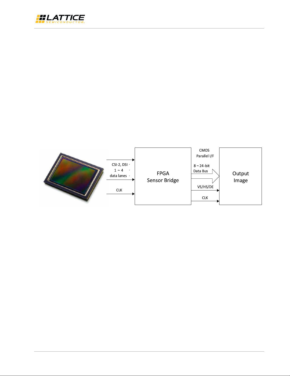
Figure 1.1 shows a conceptual model of the CMOS Sensor Bridge Design. On the left, a CMOS sensor transfers image
data to the FPGA through 1 to 4 serial data lanes; the FPGA sensor bridge merges the image data from multiple lanes
and converts them into parallel data; on the right, the image data are sent out over the parallel bus in standard video
format. Based on the known video format information, we can calculate the required bandwidth. Because the FPGA
does not buffer the video frames, the peak transfer rate of CMOS sensor input must meet the bandwidth requirement
of the output. With this presumption, we can estimate the maximum data rate and bit clock frequency of the CMOS
sensor interface.
Figure 1.1. CMOS Sensor Bridge Model
All other brand or product names are trademarks or registered trademarks of their respective holders. The specifications and information herein are subject to change without notice.
FPGA-UG-02041-1.1 5
© 2015-2018 Lattice Semiconductor Corp. All Lattice trademarks, registered trademarks, patents, and disclaimers are as listed at www.latticesemi.com/legal.
Page 6
MIPI D-PHY Bandwidth Matrix Table
User Guide
2. Video Format
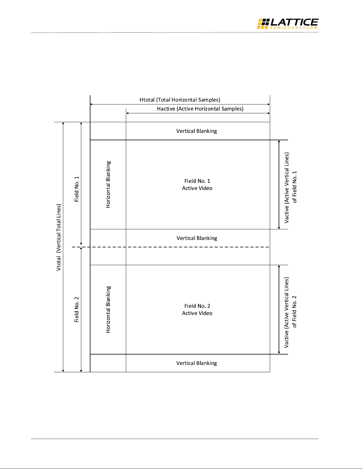
To estimate the data transfer rate, we need to understand the format of the video data transferred over the sensor
bridge. Video is composed of a series of still images. Each still image is composed of individual lines of pixel data. Figure
2.1 illustrates a conceptual interlaced video frame. The progressive video frame is similar to it except for only one field
per frame.
Figure 2.1. Interlaced Mode Video Frame Format
For digital video, either a separate Horizontal Sync (HS), Vertical Sync (VS) and Data Enable (DE) signals are used to
synchronize the video data transfer, or a special sequence embedded into the video data stream indicating the Start of
Active Video (SAV) or End of Active Video (EAV). For MIPI CSI-2, two packets structures are defined for Low Level
Protocol layer: Long packets to carry payload data, and the Short Packets for Frame Synchronization (that is Frame
Start and Frame End) and Line Synchronization (that is Line Start and Line End).
All other brand or product names are trademarks or registered trademarks of their respective holders. The specifications and information herein are subject to change without notice.
6 FPGA-UG-02041-1.1
© 2015-2018 Lattice Semiconductor Corp. All Lattice trademarks, registered trademarks, patents, and disclaimers are as listed at www.latticesemi.com/legal.
Page 7
MIPI D-PHY Bandwidth Matrix Table
User Guide
There are many characteristics of the video streams such as frame rate, interlaced vs progressive, aspect ratio,
stereoscopic, color space and color depth. We will review the major parameters that will be used in the calculation of
the data transfer rate in the later sections of the document.
2.1. Video Resolution and Pixel Clock
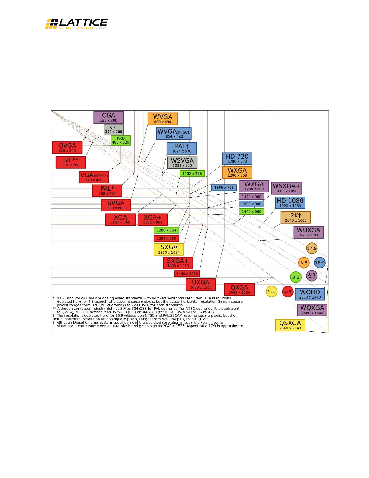
The video resolution is quoted as Width x Height, with the unit in pixels: for example, 1920x1080 means the horizontal
width is 1920 pixels and the vertical height is 1080 lines. Figure 2.2 shows the chart of the common display resolutions.
Figure 2.2. Most Common Display Resolutions
Source: https://en.wikipedia.org/wiki/File:Vector_Video_Standards4.svg
There are two major types of video format standards: SMPTE/CEA defines video standards for the Television and broadcast;
VESA Display Monitor Timing (DMT) standard defines the video standards for the computer monitors. Table 2.1 lists the
most common video resolutions. Among them, we choose HD (1280x720p), FHD (1920x1080p) and UHD (3840x2160p) as
examples to calculate the bandwidth and data rate in the later sections.
All other brand or product names are trademarks or registered trademarks of their respective holders. The specifications and information herein are subject to change without notice.
FPGA-UG-02041-1.1 7
© 2015-2018 Lattice Semiconductor Corp. All Lattice trademarks, registered trademarks, patents, and disclaimers are as listed at www.latticesemi.com/legal.
Page 8
MIPI D-PHY Bandwidth Matrix Table
Hactive
Vactive
Htotal
Vtotal
Refresh
Rate (Hz)
Pixel Freq
(MHz)
Television Video Format
EDTV
640x480p @ 59.94 Hz
640
480
800
525
59.94
25.175
720x480p @ 59.94 Hz
720
480
858
525
59.94
27
720x576p @ 50 Hz
720
576
864
625
50
27
HDTV
1280x720p @ 60 Hz
1280
720
1650
750
60
74.25
Full HD
1920x1080i @ 60 Hz
1920
1080
2200
1125
60
74.25
1920x1080p @ 60 Hz
1920
1080
2200
1125
60
148.5
UHDTV
3840x2160p @ 60 Hz
3840
2160
4400
2250
60
594
4096x2160p @ 60 Hz
4096
2160
4400
2250
60
594
Computer Monitor Format
XGA
1024x768p @ 60 Hz
1024
768
1344
806
60
65
WXGA
1280x800p @ 60 Hz
1280
800
1680
831
59.81
83.5
WXGA+
1440x900p @ 60 Hz
1440
900
1904
934
59.887
106.5
HD
1366x768p @ 60 Hz
1366
768
1792
798
59.79
85.5
HD+
1600x900p @ 60 Hz (RB)
1600
900
1800
1000
60
108
WUXGA
1920x1200p @ 60 Hz (RB)
1920
1200
2080
1235
59.95
154
WQXGA
2560x1600p @ 60 Hz (RB)
2560
1600
2720
1646
59.97
268.5
User Guide
Table 2.1. Common Video Format
Some of the image sensors can output the standard video formats by cropping or binning the pixels, the others may
output non-standard resolutions. The important thing is to obtain the information of the Total Horizontal Samples,
Total Vertical Lines and frame Refresh Rate. We will discuss how to calculate the bandwidth based on the above
information.
2.2. Color Depth
Color depth, also known as bit depth, can be either referred to as bits-per-pixel (bpp) which specifies the number of
bits used for a single pixel, or referred to as bits-per-component (bpc) which specifies the number of bits used to
represent each color component of a single pixel. Deep color supports 30/36/48-bit for three RGB colors. In this
document, the term Pixel Size is equivalent to the color depth in bits-per-pixel. For example, the pixel size of a 30-bit
deep color RGB is defined as 30 bits per pixel, or 10 bits per color component.
All other brand or product names are trademarks or registered trademarks of their respective holders. The specifications and information herein are subject to change without notice.
8 FPGA-UG-02041-1.1
© 2015-2018 Lattice Semiconductor Corp. All Lattice trademarks, registered trademarks, patents, and disclaimers are as listed at www.latticesemi.com/legal.
Page 9
MIPI D-PHY Bandwidth Matrix Table
Aligner
iDDRx
4
I/O Controller
LVDS25
LVCMOS12
LVCMOS12
50 Ω
50 Ω
DATA3_P
DATA3_N
LP3[1]
D3_p
LP3[0]
D3_n
50 Ω
50 Ω
DATA0_P
DATA0_N
LP0[1]
D0_p
LP0[0]
D0_n
50 Ω
50 Ω
CLOCK_P
CLOCK_N
LPCLK[1]
DCK_p
LPCLK[0]
DCK_n
LVDS25
LVCMOS12
LVCMOS12
LVDS25
LVCMOS12
LVCMOS12
User Guide
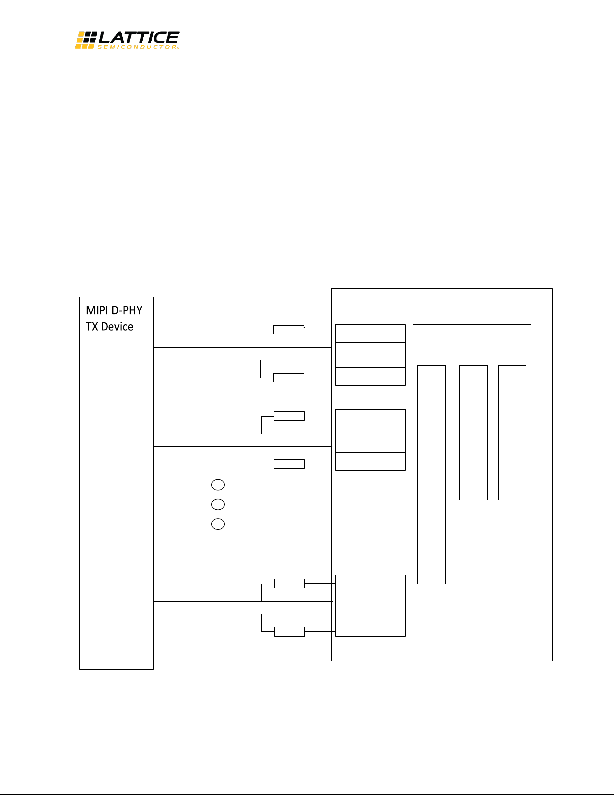
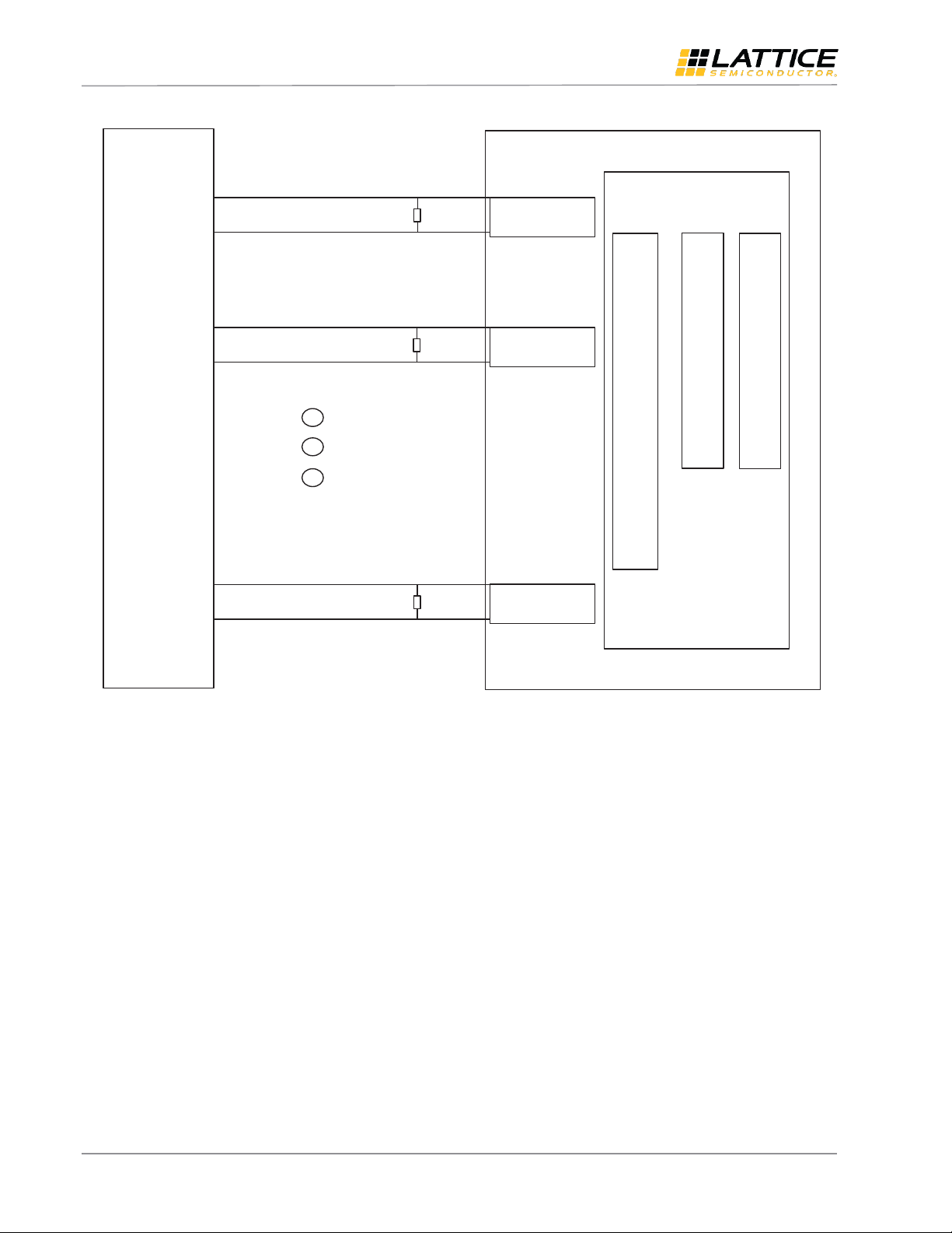
3. MIPI CSI-2/DSI Interfaces
MIPI Camera Serial Interface 2 (CSI-2) and Display serial Interface (DSI) are two of the serial interface protocols based
on MIPI D-PHY physical interface. MIPI D-PHY supports unidirectional HS (High Speed) mode and Bidirectional LP (Low
Power) mode. For the application of CMOS sensor bridge, we will only need the MIPI D-PHY receiver (RX) on the FPGA
receive interface, which allows the bridge to receive HS data on one clock lane and up to four data lanes. Figure 3.1
shows the block diagram of the Unidirectional Receive HS Mode and Bidirectional LP Mode interface. Figure 3.2 shows
the block diagram of the Unidirectional Receiver HS Mode Only interface. Figure 3.3 shows the block diagram of the
Unidirectional Transmit HS Mode and Bidirectional LP Mode interface. Figure 3.4 shows the block diagram of the
Unidirectional Transmit HS Mode Only interface.
Note: Figure 3.1 and Figure 3.2 do not apply to CrossLink since the CrossLink device uses dedicated MIPI D-PHY Input
buffers for both HS and LP mode to meet MIPI input voltage specfication. Figure 3.3 and Figure 3.4 also do not apply to
CrossLink as CrossLink’s programmable I/Os can only be configured as a MIPI D-PHY receiver (soft MIPI D-PHY). Only
the hardened MIPI D-PHY blocks can be configured as a transmitter.
For details on both Receiver/Transmitter HS and LP modes interface implementation, please refer to Lattice reference
design document MIPI D-PHY Interface IP (RD1182).
Figure 3.1. Unidirectional Receive HS Mode and Bidirectional LP Mode Interface Implementation
All other brand or product names are trademarks or registered trademarks of their respective holders. The specifications and information herein are subject to change without notice.
FPGA-UG-02041-1.1 9
© 2015-2018 Lattice Semiconductor Corp. All Lattice trademarks, registered trademarks, patents, and disclaimers are as listed at www.latticesemi.com/legal.
Page 10
MIPI D-PHY Bandwidth Matrix Table
MIPI DPHY
TX Device
LATTICE FPGA
DATA3_P
DATA3_N
D3_p
D3_n
100 Ω
LVDS25
DPHY RX Module
I/O Controller
iDDRx
4
Aligner
LVDS25
LVDS25
DATA0_P
DATA0_N
D0_p
D0_n
100 Ω
CLOCK_P
CLOCK_N
DCK_p
DCK_n
100 Ω
User Guide
Figure 3.2. Unidirectional Receive HS Mode Only Implementation
All other brand or product names are trademarks or registered trademarks of their respective holders. The specifications and information herein are subject to change without notice.
10 FPGA-UG-02041-1.1
© 2015-2018 Lattice Semiconductor Corp. All Lattice trademarks, registered trademarks, patents, and disclaimers are as listed at www.latticesemi.com/legal.
Page 11

MIPI D-PHY Bandwidth Matrix Table
Lattice FPGA
50 Ω
LVDS25E
LVCMOS12
LVCMOS12
CLOCK_P
CLOCK_N
DATA3_P
DATA3_N
DPHY TX
Module
iDDRx
4
I/O Controller
LVDS25E
LVCMOS12
LVCMOS12
LVCMOS12
LVCMOS12
330 Ω
DATA0_P
DATA0_N
MIPI DPHY
RX Device
LVDS25E
330 Ω
50 Ω
50 Ω
330 Ω
330 Ω
50 Ω
50 Ω
330 Ω
330 Ω
50 Ω
User Guide
FPGA-UG-02041-1.1 11
Figure 3.3. Unidirectional Transmit HS Mode and Bidirectional LP Mode Interface Implementation
© 2015-2018 Lattice Semiconductor Corp. All Lattice trademarks, registered trademarks, patents, and disclaimers are as listed at www.latticesemi.com/legal.
All other brand or product names are trademarks or registered trademarks of their respective holders. The specifications and information herein are subject to change without notice.
Page 12

MIPI D-PHY Bandwidth Matrix Table
Lattice FPGA
70 Ω
LVDS25E
CLOCK_P
CLOCK_N
DATA_P
DATA_N
DPHY TX
Module
iDDRx
4
I/O Controller
LVDS25E
LVDS25E
330 Ω
330 Ω
330 Ω
330 Ω
330 Ω
330 Ω
DATA_P
MIPI DPHY
RX Device
70 Ω
DATA_N
70 Ω
70 Ω
70 Ω
70 Ω
70 Ω resistors
connected to
ground for HS-only
mode.
User Guide
12 FPGA-UG-02041-1.1
Figure 3.4. Unidirectional Transmit HS Mode Only Implementation
All other brand or product names are trademarks or registered trademarks of their respective holders. The specifications and information herein are subject to change without notice.
© 2015-2018 Lattice Semiconductor Corp. All Lattice trademarks, registered trademarks, patents, and disclaimers are as listed at www.latticesemi.com/legal.
Page 13

MIPI D-PHY Bandwidth Matrix Table
FS
P1 P2
FE
P4 LSBsP3 …. P637 P638 P640 LSBsP639
P1 P2 P4 LSBsP3 …. P637 P638 P640 LSBsP639
P1 P2 P4 LSBsP3 …. P637 P638 P640 LSBsP639
P1 P2 P4 LSBsP3 …. P637 P638 P640 LSBsP639
P1 P2 P4 LSBsP3 …. P637 P638 P640 LSBsP639
P1 P2 P4 LSBsP3 …. P637 P638 P640 LSBsP639
P1 P2 P4 LSBsP3 …. P637 P638 P640 LSBsP639
P1 P2 P4 LSBsP3 …. P637 P638 P640 LSBsP639
P1 P2 P4 LSBsP3 …. P637 P638 P640 LSBsP639
P1 P2 P4 LSBsP3 …. P637 P638 P640 LSBsP639
P1 P2 P4 LSBsP3 …. P637 P638 P640 LSBsP639
P1 P2 P4 LSBsP3 …. P637 P638 P640 LSBsP639
P5
P5
P5
P5
P5
P5
P5
P5
P5
P5
P5
P5
Packer Header
, PH
Packer Footer
, PF
Data
A2
P1[9:2] (A)
A3 A4 A5 A6 A7 A8 A9
P1
[1:0]P2[1:0]P3[1:0]P4[1:0]
A0 A1 B0 B1 C0 C1 D0 D1
P5[9:2] (E)
B2 B3 B4 B5 B6 B7 B8 B9
P2[9:2] (B) P3[9:2] (C)
P4[9:2] (D)
8 bits
Byte Values Transmitted LS Bit First
E2 E3 E4 E5 E6 E7 E8 E9
8 bits 8 bits
F2 F3 F4 F5 F6 F7 F8 F9
P6[9:2] (F)
G2 G3 G4 G5 G6 G7 G8 G9
P7[9:2] (G)
D2 D3 D4 D5 D6 D7 D8 D9
8 bits
G2 C3 C4 C5 C6 C7 C8 C9
Line Start
Line End
P1[9:2]
P2[9:2]
P3[9:2]
P4[9:2]
P4
[1:0]P3[1:0]
LSBs
P2
[1:0]P1[1:0]
P5[9:2]
P6[9:2]
P636
[1:0]
P635
[1:0]
P634
[1:0]
P633
[1:0]
LSBs
P637[9:2]
P638[9:2]
P639[9:2]
P640[9:2]
LSBs
P640
[1:0]
P639
[1:0]
P638
[1:0]
P637
[1:0]
User Guide
4. Packetizing
The MIPI CSI-2 supports YUV, RGB or RAW data with varying pixel formats from 6 to 24 bits per pixel. In the transmitter
the pixels are packed into bytes (Pixel-to-byte Packing) before sending the data to Low Level Protocol layer; in the
receiver the bytes received from the Low Level Protocol layer are unpacked into pixel (Byte-to-pixel Unpacking). One
CSI-2 long packet shall contain one line of image data. The total size of data within a long packet for all data types shall
be a multiple of eight bits (byte). Figure 4.1 shows an example of packing four 10-bit pixel data, or RAW10, into five
bytes to look like 8-bit data format.
© 2015-2018 Lattice Semiconductor Corp. All Lattice trademarks, registered trademarks, patents, and disclaimers are as listed at www.latticesemi.com/legal.
All other brand or product names are trademarks or registered trademarks of their respective holders. The specifications and information herein are subject to change without notice.
FPGA-UG-02041-1.1 13
Figure 4.1. An Example of RAW10 Transmissions on CSI-2 Bus
Page 14

MIPI D-PHY Bandwidth Matrix Table
Data Format
Odd/Even Lines
Pixels
Bytes
Bits
YUV420 8-bit
Odd 2 2
16
Even 2 4
32
YUV420 10-bit
Odd 4 5
40
Even 4 10
80
YUV422 8-bit — 2 4 32
YUV422 10-bit — 2 5 40
RGB888 — 1 3 24
RGB666 — 4 9 72
RGB565 — 1 2 16
RGB555 — 1 2 16
RGB444 — 1 2 16
RAW6 — 4 3 24
RAW7 — 8 7 56
RAW8 — 1 1 8
RAW10 — 4 5 40
RAW12 — 2 3 24
RAW14 — 4 7 56
User Guide
Table 4.1 specifies the packet size constraints for the supported data formats. The length of each packet must be a
multiple of the values in the table. For simplicity, all data format examples are single lane configurations.
Table 4.1. CSI-2 Packet Size Constraints*
*Note: RGB555 and RGB444 data should be made to look like RGB565 data by inserting padding bits to the LSBs of each color
component.
4.1. xMulti-lane
MIPI CSI-2 is lane-scalable. Applications requiring more bandwidth than that provided by one data lane, or those trying
to avoid high clock rates, can expand the data path to two, three, or four lanes wide and obtain appro ximately linear
increases in peak bus bandwidth
All other brand or product names are trademarks or registered trademarks of their respective holders. The specifications and information herein are subject to change without notice.
14 FPGA-UG-02041-1.1
© 2015-2018 Lattice Semiconductor Corp. All Lattice trademarks, registered trademarks, patents, and disclaimers are as listed at www.latticesemi.com/legal.
Page 15

MIPI D-PHY Bandwidth Matrix Table
User Guide
5. Bandwidth and Data Rate
This section provides the definitions of terms used in video performance and summarizes the process of calculating
bandwidth and data transfer rate.
Pixel Clock – the time base in MHz at which individual pixels are transmitted
Bandwidth – the capacity required in Mbps of a given system to pass a specific frequency
Data Rate – the data flow throughput in bits per second of the transport layer
5.1. Bandwidth and Data Rate Calculation
5.1.1. Pixel Clock
If the video format is standard, the pixel clock frequency can be obtained from the SMPTE/CEA or VESA standards. You
can also calculate the pixel clock frequency using the following equation:
Pixel Clock Frequency = Total Horizontal Samples * Total Vertical Lines * Refresh Rate
The Total Horizontal Samples and Total Vertical Lines include blanking period. The Refresh Rate may be referred to as
Frame Rate or Vertical Frequency
5.1.2. Total Data Rate or Bandwidth
The bandwidth of a given video format is simply a product of the Pixel Clock Frequency and Pixel Size in bits. The total
data rate of the CMOS sensor interface must match the bandwidth.
Total Data Rate (Bandwidth) = Pixel Clock Frequency * Pixel Size (in bits)
5.1.3. Data Rate per Lane
The per-lane data rate (Line Rate) is the total data rate (bandwidth) divided by the number of lanes. CSI-2 can support
up to four data lanes.
Data Rate per Lane = Total Data Rate (Bandwidth)/Number of Data Lane
5.1.4. Bit Clock
Because the MIPI data lane is a Double Data Rate interface, the CSI-2 Bit Clock frequency is ½ of the Data Rate per Lane
Bit Clock Frequency = Data Rate per Lane/2
5.2. Examples
5.2.1. Example 1: 1920x1080p@60Hz, RAW10, 2-lane
Total Horizontal Samples = 2200, Total Vertical Lines = 1125
Pixel Clock Frequency = 2200 x 1125 x 60 = 148.5 MHz
Bandwidth (Total Data Rate) = 148.5 MHz * 10-bit = 1.485 Gbps
Line Rate (Data Rate per Lane) = 1.485 Gbps/2-lane = 742.5 Mbps
MIPI Bit Clock Frequency = 742.5/2 = 371.25 MHz
5.2.2. Example 2: 3840x2160@30Hz, RAW8, 4-lane
Total Horizontal Samples = 4400, Total Vertical Lines = 2250
Pixel Clock Frequency = 4400 x 2250 * 30 = 297 MHz
Bandwidth (Total Data Rate) = 297 MHz * 8-bit = 2.376 Gbps
Line Rate (Data Rate per Lane) = 2.376 Gbps/4-lane = 594 Mbps
MIPI Bit Block Frequency = 594/2 = 297 MHz
All other brand or product names are trademarks or registered trademarks of their respective holders. The specifications and information herein are subject to change without notice.
FPGA-UG-02041-1.1 15
© 2015-2018 Lattice Semiconductor Corp. All Lattice trademarks, registered trademarks, patents, and disclaimers are as listed at www.latticesemi.com/legal.
Page 16

MIPI D-PHY Bandwidth Matrix Table
MachXO2/
MachXO3L
LatticeECP3 EA
ECP5/ECP5-5G
CrossLink3
MIPI D-PHY
Rx Implementations
HS Mode
LVDS25
VCCIO = 2.5 V
or 3.3 V
Internal 100 Ω
differential
termination.
LVDS25
VCCIO = 2.5v
or 3.3v
Internal 100 Ω
differential
termination.
LVDS25
VCCIO = 2.5 V
or 3.3 V
Internal 100 Ω
differential
termination.
Dedicated
MIPI D-PHY
inputs buffer
Internal 100 Ω
differential
termination
LP Mode
LVCMOS12
VCCIO = 1.2 V
LVCMOS12
VCCIO = 1.2 V
LVCMOS12
VCCIO = 1.2 V
Dedicated
MIPI D_PHY
input buffer
MIPI D-PHY Tx
Implementations
HS Mode:
LVDS25E
LVDS25E or
LVCMOS33D2
LVDS25E or
LVCMOS33D2
—
LP Mode:
LVCMOS12
VCCIO = 1.2 V
LVCMOS12
VCCIO = 1.2 V
LVCMOS12
VCCIO = 1.2 V
—
DDR Gearing Ratio
X4
X2
X2
X8
Number of D-PHY
Rx
Up to two RX DPHYs; Bank 2 only.
Up to two RX DPHYs. Only two
clock divider
primitives, one on
Bank 2 or 3 (right),
one on Bank 6 or 7
(left)
Up to 4 RX D-PHYs
(left and right sides)
Four dedicated
Clock Divider
(CLKDVI) available
Limited by PIO pairs
and clock divider
available in Bank 1
and 2 only
Tx
TX D-PHY max
limited by PIO A/B
pairs; Bank 0 only
TX D-PHY maximum
limited by PIO pairs
available in Bank 2,
3, 6 and 7 if CLKDIV
is shared on each
side. If TX D-PHY on
side, can only have
RX D-PHY on the
other
TX D-PHY maximum
limited by PIO
pairs, available in
the left and right
banks.
—
Number of Lanes
Depends on data
rate and number of
PIO A/B pairs
available. DDRX4
requires A/B pair
and Edge clock
Depends on data
rate and number of
PIO A/B pairs
available. DDRX4
requires A/B pair
and Edge clock
Depends on data
rate and number of
PIO A/B pairs
available. DDRX4
requires A/B pair
and Edge clock
4 lanes max
RX Performance1
523 Mbps
467 Mbps
467 Mbps
898 Mbps
TX Performance1
728 Mbps
698 Mbps
820 Mbps
1250 Mbps
User Guide
6. Device Selection
This section summarizes Lattice FPGA families that support MIPI interface with external components as described in
the MIPI CSI-2/DSI Interfaces section.
6.1. Hardware Features
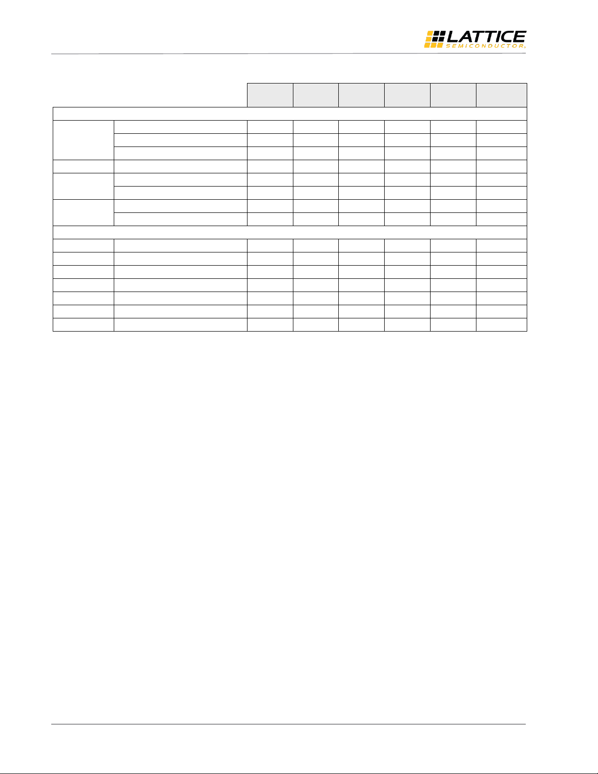
Table 6.1 highlights the features of MIPI D-PHY hardware implementation using MachXO2, MachXO3L, LatticeECP3,
ECP5/ECP5-5G and Crosslink device families. For more details on MIPI D-PHY Receiver and Transmitter resource
utilization and design performance, refer to the MIPI D-PHY Interface IP (RD1182) document.
Table 6.1. MIPI Soft D-PHY RX/TX Hardware Comparison
16 FPGA-UG-02041-1.1
All other brand or product names are trademarks or registered trademarks of their respective holders. The specifications and information herein are subject to change without notice.
© 2015-2018 Lattice Semiconductor Corp. All Lattice trademarks, registered trademarks, patents, and disclaimers are as listed at www.latticesemi.com/legal.
Page 17

MIPI D-PHY Bandwidth Matrix Table
User Guide
Notes:
1. Rx and Tx Performance is calculated from the data sheet External Timing Table using IDDRX2/X4/X8 and ODDRX2/X4/X8with
data and clock centered aligned. See the MIPI Data Rate Calculation section for the calculations based on current data sheet.
Re-calculate to confirm these values with the most up to date data sheet specification
2. If LVCMOS33D is used instead of LVDS25E, external resistors shown in Figure 3.3 and Figure 3.4 should be adjusted to modulate
common mode voltage level.
3. CrossLink has two hardened MIPI IPs on the top side of the chip, and has dedicated IO associated with harded IP. Regard to
MIPI D-PHY interface implementation, on the receiver side it has hardened IP offering as well as soft IP offering, but on the
transmitter side it only offers hardened IP implemtation.
All other brand or product names are trademarks or registered trademarks of their respective holders. The specifications and information herein are subject to change without notice.
© 2015-2018 Lattice Semiconductor Corp. All Lattice trademarks, registered trademarks, patents, and disclaimers are as listed at www.latticesemi.com/legal.
FPGA-UG-02041-1.1 17
Page 18

MIPI D-PHY Bandwidth Matrix Table
Setup Time
Hold Time
0.233
0.287
MachXO2 Data Sheet Rev. 3.3 at 756 Mbps
Generic DDRX4 Inputs with Clock and Data Centered at Pin Using PCLK Pin for Clock Input – GDDRX4_RX.ECLK.Centered
t
SU
Input Data Setup Before CLK
MachXO2-640U,
MachXO2-1200/U and
larger devices,
bottom side only
t
HO
Input Data Hold After CLK
f
DATA
DDRX4 Serial Input Data
Speed
f
DDRX4
DDRX2 ECLK Frequency
f
SCLK
SCLK Frequency
0.233
0.287
756
378
95
—
—
—
——0.219
0.287
630
315
79
—
—
—
——0.198
0.344
524
262
66
—
—
—
—
—
Mbps
MHz
MHz
ns
ns
User Guide
7. MIPI Data Rate Calculation
This section shows the calculations of the maximum data rate that can be achieved on Lattice FPGA products. The
values are based on data sheet specification of DDRX2/X4/X8 with clock and data center-aligned. These are MIPI
Alliance Specification compliant with ±0.15 UI setup/hold window on the receiver at ≤1 Gbps and ±0.15 UI skew
window on the transmitter at ≤1 Gbps.
This section also provides the method of calculating the windows if higher data rate is desired. The window for higher
data rate does meet MIPI Alliance Specification, but can still be practical in the user’s implementation. Check the latest
data sheet on the maximum data rate each Lattice FPGA device family can achieve.
7.1. FPGA Receiver Interface
7.1.1. MachXO2/MachXO3L
Maximum MIPI compliance data rate calculation for MachXO2/MachXO3L:
Max (0.233, 0.287) = 0.15 x UI
UI = 0.287/0.15 = 1.913 ns
Max Data Rate = 1/UI = 1/1.913 = 523 Mbps (at 0.15 UI)
Figure 7.1. MachXO2/MachXO3L Maximum Data Rate
All other brand or product names are trademarks or registered trademarks of their respective holders. The specifications and information herein are subject to change without notice.
18 FPGA-UG-02041-1.1
© 2015-2018 Lattice Semiconductor Corp. All Lattice trademarks, registered trademarks, patents, and disclaimers are as listed at www.latticesemi.com/legal.
Page 19

MIPI D-PHY Bandwidth Matrix Table
Setup Time
Hold Time
0.321
0.321
LatticeECP3 Data Sheet Rev. 2.8EA at 800 Mbps
Generic DDRX2 Inputs with Clock and Data (>10 Bits Wide) Centered at Pin (GDDRX2_RX.ECLK.Centered) Using PCLK Pin for Clock Input
t
SUGDDR
t
HOGDDR
Data Hold After CLK
f
MAX_GDDR
DDRX2 Clock Frequency
321
—
405
321
—
— 403
—
325
403
—
—
ps
MHz
ps
Data Setup B efore CLK ECP3-150EA
ECP3-150EA
ECP3-150EA
Left and Right Sides
t
SUGDDR
Data Setup B efore CLK
t
HOGDDR
Data Hold After CLK
—
—
—
335
335
405 —
—
—
425
425
325
ps
ps
MHz
DDRX2 Clock Frequency ECP3-70EA/95EA
ECP3-35EA
ECP3-35EA
t
SUGDDR
t
HOGDDR
Data Hold After CLK
321
—321
— 403
—403
—
ps
ps
Data Setup Before CLK ECP3-70EA/95EA
ECP3-70EA/95EA
f
MAX_DDR
t
SUGDDR
Data Setup B efore CLK
t
HOGDDR
Data Hold After CLK
—
—
—
335
335
405 —
—
—
425
425
325
ps
ps
MHz
DDRX2 Clock Frequency ECP3-35EA
ECP3-17EA
ECP3-17EA
f
MAX_GDDR
— 405 — 325 MHz
DDRX2 Clock Frequency ECP3-17EA
f
MAX_GDDR
471
—
280
471
—
—
—
—
—
535
535
250
535
—535
—
—
—
—
535
535
250
— 250
User Guide
7.1.2. LatticeECP3
Maximum MIPI compliance data rate calculation for LatticeECP3:
Max (0.321, 0.321) = 0.15 x UI
UI = 0.321/0.15 = 2.14 ns
Max Data Rate = 1/UI = 1/2.14 = 467 Mbps (at 0.15 UI)
FPGA-UG-02041-1.1 19
All other brand or product names are trademarks or registered trademarks of their respective holders. The specifications and information herein are subject to change without notice.
© 2015-2018 Lattice Semiconductor Corp. All Lattice trademarks, registered trademarks, patents, and disclaimers are as listed at www.latticesemi.com/legal.
Figure 7.2. LatticeECP3 Maximum Data Rate
Page 20
MIPI D-PHY Bandwidth Matrix Table
Setup Time
Hold Time
0.321
0.321
ECP5/ECP5-5G Data Sheet Rev. 1.9 at 800 Mbps
Generic DDRX2 Inputs with Clock and Data Centered at Pin (GDDRX2_RX.ECLK.Centered) Using PCLK Clock Input, Left and Right Sides Only
t
SU_GDDRX2_CENTERED
Data Setup before CLK Input
t
HD_GDDRX2_CENTERED
f
DATA_GDDRX2_CENTERED
GDDRX2 Data Rate
f
MAX_GDDRX2_CENTERED
GDDRX2 CLK Frequency (ECLK)
0.321
0.321
800
400
—
—
——0.403
0.403
700
350
—
—
——0.471
0.471
624
312
—
—
—
—
Mb/s
MHz
ns
ns
Data Hold after CLK Input
All Devices
All Devices
All Devices
All Devices
User Guide
7.1.3. ECP5/ECP5-5G
Maximum MIPI compliance data rate calculation for ECP5/ECP-5G:
Max (0.321, 0.321) = 0.15 x UI
UI = 0.321/0.15 = 2.14 ns
Max Data Rate = 1/UI = 1/2.14 = 467 Mbps (at 0.15 UI)
Figure 7.3. ECP5/ECP5-5G Maximum Data Rate
All other brand or product names are trademarks or registered trademarks of their respective holders. The specifications and information herein are subject to change without notice.
20 FPGA-UG-02041-1.1
© 2015-2018 Lattice Semiconductor Corp. All Lattice trademarks, registered trademarks, patents, and disclaimers are as listed at www.latticesemi.com/legal.
Page 21

MIPI D-PHY Bandwidth Matrix Table
Device Family
Max Data Rate
Tsu/Thd Window
MachXO2
756 Mbps
0.217 UI
MachXO3L
900 Mbps
0.285 UI
LatticeECP3
800 Mbps
0.257 UI
ECP5
800 Mbps
0.257 UI
ECP5-5G
800 Mbps
0.257 UI
CrossLink Soft D-PHY
1200 Mbps at VID =140 mv
0.20 UI
General Purpose I/O MIPI D-PHY Rx with 1:8 or 1:16 Gearing
t
SU_GDDRX_MP
Input Data Set-Up Before CLK
900 Mb/s < Data Rate ≤
1.2 Gb/s &
VID = 140 mV
0.200 — UI
600 Mb/s < Data Rate ≤
900 Mb/s &
VID = 140 mV
0.150 — UI
Data Rate ≤ 600 Mb/s &
VID = 70 mV
0.150 — UI
t
HD_GDDRX_MP
Input Data Hold After CLK
900 Mb/s < Data Rate ≤
1.2 Gb/s &
VID = 140 mV
0.200 — UI
600 Mb/s < Data Rate ≤
900 Mb/s &
VID = 140 mV
0.150 — UI
Data Rate ≤ 600 Mb/s &
VID = 70 mV
0.150 — UI
f
MAX_GDDRX_MP
Frequency for ECLK3
csfBGA81, ctfBGA80,
ckfBGA80, ucfBGA64
—
600
MHz
WLCSP36
—
500
MHz
User Guide
7.1.4. CrossLink Soft D-PHY
Maximum MIPI compliance data rate calculation for CrossLink:
1200 Mbps at V
900 Mbps at V
600 Mbps at V
CrossLink Data Sheet Rev. 1.4
= 140 mv
ID
=140 mv
ID
=70 mv
ID
Figure 7.4. CrossLink Maximum Data Rate
7.1.5. t
SU/tHD
Valid Window at Higher Data Rate
For data rate higher than specified above, the tSU/tHD window may exceed the 0.15 UI specified in the MIPI Alliance
Specification.
To calculate the window, the following equation can be used:
tSU/tHD Window = max(tSU/tHD) / (1 / Data Rate)
For 800 Mbps, 1 / Data Rate = 1.25 ns.
The maximum data rate each device can support on the receiver is limited to the data rate supported with
IDDRX2/X4/X8 with center-aligned data. This is summarized in Table 7.1.
Table 7.1. tSU/tHD Window for Higher Data Rate
All other brand or product names are trademarks or registered trademarks of their respective holders. The specifications and information herein are subject to change without notice.
FPGA-UG-02041-1.1 21
© 2015-2018 Lattice Semiconductor Corp. All Lattice trademarks, registered trademarks, patents, and disclaimers are as listed at www.latticesemi.com/legal.
Page 22

MIPI D-PHY Bandwidth Matrix Table
Setup Time
Hold Time
0.455
0.455
At 756 Mbps, ½ UI = 0.661
Tskew = 0.661 - 0.445 = 0.206
MachXO2 Data Sheet Rev. 3.3 at 756 Mbps
Generic DDRX4 Outputs with Clock and Data Cen tered at Pin Using PCLK Pin for Clock Input – GDDRX4TX.ECLK.Centered
t
DVB
Output Data Valid Before CLK Output
MachXO2-640U,
MachXO2-1200/U
and larger devices,
top side only
t
DVA
Output Data Hold After CLK Output
f
DATA
DDRX4 Serial Output Data Speed
f
DDRX4
DDRX4 ECLK Frequency
(minimum limited by PLL)
f
SCLK
SCLK Frequency
0.455
0.455
756
378
95
—
—
—
—
—
0.570
0.570
630
315
79
—
—
—
—
—
0.710
0.710
524
262
66
—
—
—
—
—
Mbps
MHz
MHz
ns
ns
User Guide
7.2. FPGA Transmitter Interface
7.2.1. MachXO2/MachXO3L
Maximum MIPI compliance data rate calculation for MachXO2/MachXO3L:
0.206 = 0.15 x UI
UI = 0.206/0.15 = 1.373 ns
Max Data Rate = 1/UI = 1/1.373 = 728 Mbps (at 0.15 UI)
Figure 7.5. MachXO2 Maximum Data Rate
All other brand or product names are trademarks or registered trademarks of their respective holders. The specifications and information herein are subject to change without notice.
22 FPGA-UG-02041-1.1
© 2015-2018 Lattice Semiconductor Corp. All Lattice trademarks, registered trademarks, patents, and disclaimers are as listed at www.latticesemi.com/legal.
Page 23

MIPI D-PHY Bandwidth Matrix Table
Setup Time
Hold Time
0.285
0.285
At 1000 Mbps, ½ UI = 0.5
Tskew = 0.5 - 0.285 = 0.215
LatticeECP3 Data Sheet Rev. 2.8EA at 1000 Mbps
Generic DDRX2 Output with Clock and Data (>10 Bits Wide) Centered at Pin Using PLL (GDDRX2_TX.PLL.Centered)
t
DVBGDDR
f
DVAGDDR
Data Valid After CLK
f
MAX_GDDR
DDRX2 Clock Frequency
285
—
500
285
—
— 370
—
420
370
—
— 431
—
375
432
—
—
ps
MHz
ps
Data Valid Before CLK All ECP3EA Devices
All ECP3EA Devices
All ECP3EA Devices
Left and Right Sides
User Guide
7.2.2. LatticeECP3
Maximum MIPI compliance data rate calculation for LatticeECP3:
0.215 = 0.15 x UI
UI = 0.215/0.15 = 1.433 ns
Max Data Rate = 1/UI = 1/1.433 = 698 Mbps (at 0.15 UI)
Figure 7.6. LatticeECP3 Maximum Data Rate
All other brand or product names are trademarks or registered trademarks of their respective holders. The specifications and information herein are subject to change without notice.
FPGA-UG-02041-1.1 23
© 2015-2018 Lattice Semiconductor Corp. All Lattice trademarks, registered trademarks, patents, and disclaimers are as listed at www.latticesemi.com/legal.
Page 24

MIPI D-PHY Bandwidth Matrix Table
Setup Time
Hold Time
0.442
0.442
At 800 Mbps, ½ UI = 0.625
Tskew = 0.625 - 0.442 = 0.183
ECP5/ECP5-5G Data Sheet Rev. 1.9 at 800 Mbps
Generic DDRX2 Outputs with Clock and Data Centered at Pin (GDDRX2_TX.ECLK.Centered) Using PCLK Clock Input, Left and Right Sides Only
t
SU_GDDRX2_centered
Data Output Valid Before CLK Output
t
HD_GDDRX2_centered
f
DATA_GDDRX2_centered
GDDRX2 Data Rate
f
MAX_GDDRX2_centered
GDDRX2 CLK Frequency (ECLK)
0.442
—
800
400
—
—
—
0.442
0.56
—
700
350
—
—
—
0.56
0.676
—
624
312
—
—
—
0.676
Mb/s
MHz
ns + ½ UI
Data Output Valid After CLK Output
All Devices
All Devices
All Devices
All Devices
ns + ½ UI
Device Family
Max Data Rate
Tsu/Thd Window
MachXO2
756 Mbps
0.155 UI
MachXO3L
900 Mbps
0.185 UI
LatticeECP3
800 Mbps
0.172 UI
ECP5
800 Mbps
<= 0.150 UI
ECP5-5G
800 Mbps
<= 0.150 UI
User Guide
7.2.3. ECP5/ECP5-5G
Maximum MIPI compliance data rate calculation for ECP5/ECP5-5G:
0.183 = 0.15 x UI
UI = 0.183/0.15 = 1.22 ns
Max Data Rate = 1/UI = 1/1.22 = 820 Mbps (at 0.15 UI)
Figure 7.7. ECP5/ECP5-5G Maximum Data Rate
7.2.4. Tskew Window at Higher Data Rate
For data rate higher than specified above, the tskew window may exceed the 0.15UI specified in the MIPI Alliance
Specification.
To calculate the window, the following equation can be used:
½ UI = ½ * (1 / Data Rate)
Tskew Window = (½ UI – min (tDVA, tDVB) / UI)
For 800 Mbps, 1 / Data Rate = 1.25 ns.
The maximum data rate each device can support on the receiver is limited to the data rate supported with
IDDRX2/X4/X8 with center-aligned data. This can be summarized in Table 7.2.
Table 7.2. Tskew Window for Higher Data Rate
© 2015-2018 Lattice Semiconductor Corp. All Lattice trademarks, registered trademarks, patents, and disclaimers are as listed at www.latticesemi.com/legal.
All other brand or product names are trademarks or registered trademarks of their respective holders. The specifications and information herein are subject to change without notice.
24 FPGA-UG-02041-1.1
Page 25

MIPI D-PHY Bandwidth Matrix Table
MachXO2 and MachXO3L
(523 Mbps for RX and 728
Mbps for TX I/O)
LatticeECP3 (467 Mbps for RX
and 698 Mbps for TX I/O)
ECP5/ECP5-5G (467 Mbps
for RX and 820 Mbps for
TX I/O)
CrossLink (898 Mbps for RX
and 1250 Mbps for TX I/O)
Resolution
Frame
Rate
Pixel
Clock
Color
Depth
Total
Data
Rate
Lane
Number
Line
Rate
Bit
Clock
Lane
Number
Line
Rate
Bit
Clock
Lane
Number
Line
Rate
Bit
Clock
Lane
Number
Line
Rate
Bit
Clock
Hz
MHz
Bits
Mbps
Mbps
MHz
Mbps
MHz
Mbps
MHz
Mbps
MHz
HD
1280x720p
(1650x750)
60
74.25
8
594 2 297
148.5 2 297
148.5
2
297
148.5 1 594
297
10
742.5 2 371
185.6 2 371
185.6
2
371
185.6 1 742.5
371
16
1188 4 297
148.5 4 297
148.5
4
297
148.5 2 594
297
18
1336.5
4
334
167 4 334
167 4 334
167 2 668
334
24
1782
4
445.5
223 4 445.5
223
4
445.5
223 2 891
445.5
120
148.5
8
1188 4 297
148.5 4 297
148.5
4
297
148.5 2 594
297
10
1485 4 371
185.6 4 371
185.6
4
371
185.6 2 742.5
371
16
2376 — — — — — — — — — — — —
18
2673 — — — — — — — — — — — —
24
3564 — — — — — — — — — — — —
240
297
8
2376 — — — — — — — — — 4
594
297
10
2970 — — — — — — — — — 4
742.5
371
16
4752 — — — — — — — — — — — —
18
5346 — — — — — — — — — — — —
24
7128 — — — — — — — — — — — —
User Guide
7.3. MIPI D-PHY Lane Number Selection Matrix Table
Table 7.3 lists the selection of MIPI D-PHY Lane number and Line rate versus the Total Data Rate required by each video format. For clarity, this Matrix table only chooses
three common resolutions and the major color depths as examples. The lane number and line rate for other video formats can be calculated using the equations listed in
Bandwidth and Data Rate section.
Table 7.3. MIPI D-PHY Interface Lane Number and Line Rate Selection Example Matrix Table
FPGA-UG-02041-1.1 25
All other brand or product names are trademarks or registered trademarks of their respective holders. The specifications and information herein are subject to change without notice.
© 2015-2018 Lattice Semiconductor Corp. All Lattice trademarks, registered trademarks, patents, and disclaimers are as listed at www.latticesemi.com/legal.
Page 26

MIPI D-PHY Bandwidth Matrix Table
MachXO2 and MachXO3L
(523 Mbps for RX and 728
Mbps for TX I/O)
LatticeECP3 (467 Mbps for RX
and 698 Mbps for TX I/O)
ECP5/ECP5-5G (467 Mbps
for RX and 820 Mbps for
TX I/O)
CrossLink (898 Mbps for RX
and 1250 Mbps for TX I/O)
Resolution
Frame
Rate
Pixel
Clock
Color
Depth
Total
Data
Rate
Lane
Number
Line
Rate
Bit
Clock
Lane
Number
Line
Rate
Bit
Clock
Lane
Number
Line
Rate
Bit
Clock
Lane
Number
Line
Rate
Bit
Clock
Hz
MHz
Bits
Mbps
Mbps
MHz
Mbps
MHz
Mbps
MHz
Mbps
MHz
FHD
1920x1080p
(2200x1125)
60
148.5
8
1188 4 297
148.4 4 297
148.5
4
297
148.5 2 594
297
10
1485 4 371
185.6 4 371
185.6
4
371
185.6 — —
—
16
2376 — — — — — — — — — 4
594
297
18
2673 — — — — — — — — — — — —
24
3564 — — — — — — — — — — — —
120
297
8
2376 — — — — — — — — — 4
594
297
10
2970 — — — — — — — — — 4
742.5
371
16
4752 — — — — — — — — — — — —
18
5346 — — — — — — — — — — — —
24
7128 — — — — — — — — — — — —
UHD
3840x2160p
(4400x2250)
30
297
8
2376
4
5941
297 4 5941
297
4
5941
297 4 594
297
10
2970 — — — 4
742.52
371
4
742.53
371 4 742.5
371
16
4752 — — — — — — — — — — — —
18
5346 — — — — — — — — — — — —
24
7128 — — — — — — — — — — — —
60
594
8
4752 — — — — — — — — — 4
1188
594
10
5940 — — — — — — — — —
16
9504 — — — — — — — — — — — —
18
10692 — — — — — — — — — — — —
24
14256 — — — — — — — — — — — —
User Guide
Notes:
1. Meeting Tx MIPI Alliance specification, Rx is not meeting MIPI Alliance requirement, and Tsu/Thd window can be calculated based on the tSU/tHD Valid Window at Higher Data
Rate section. Rx side is 0.17 UI (0.287 ns * 594 Mbps) for MachXO2/MachXO3L, 0.19 UI (0.321 ns * 594 Mbps) for LatticeECP3 andECP5/ECP-5G.
2. Both Rx and Tx side not meeting MIPI Alliance specification, Rx Tsu/Thd window and Tx Tskew window can be calculated based on the tSU/tHD Valid Window at Higher Data
Rate and Tskew Window at Higher Data Rate sections. Tx side is 0.16 UI (0.215 ns * 742.5 Mbps), Rx side is 0.24 UI (0.321 ns * 742.5 Mbps).
3. Meeting Tx MIPI Alliance specification, Rx is not meeting MIPI Alliance requirement, and Tsu/Thd window can be calculated based on tSU/tHD Valid Window at Higher Data Rate.
Rx side is 0.24 UI (0.321 ns * 742.5 Mbps).
26 FPGA-UG-02041-1.1
All other brand or product names are trademarks or registered trademarks of their respective holders. The specifications and information herein are subject to change without notice.
© 2015-2018 Lattice Semiconductor Corp. All Lattice trademarks, registered trademarks, patents, and disclaimers are as listed at www.latticesemi.com/legal.
Page 27

Reference
Date
Version
Change Summary
May 2018
1.1
Changed document number from UG110 to FPGA-UG-02041.
Updated document template.
Updated MIPI CSI-2/DSI Interfaces section. Added Figure 3.3 and Figure 3.4.
Updated Packetizing section. Updated Figure 4.1.
Updated Bandwidth and Data Rate section. Revised content structure.
Updated Device Selection section.
Updated Table 6.1.
Updated and moved Table 7.3. MIPI D-PHY Interface Lane Number and Line
Rate Selection Example Matrix Table.
Removed (the previous) Figure 7 and Figure 8.
Added MIPI Data Rate Calculation section.
June 2015
1.0
Initial release.
MIPI D-PHY Interface IP (RD1182)
Technical Support
For assistance, submit a technical support case at www.latticesemi.com/techsupport.
Revision History
MIPI D-PHY Bandwidth Matrix Table
User Guide
© 2015-2018 Lattice Semiconductor Corp. All Lattice trademarks, registered trademarks, patents, and disclaimers are as listed at www.latticesemi.com/legal. All other brand or product names are
FPGA-UG-02041-1.1 27
trademarks or registered trademarks of their respective holders. The specifications and information herein are subject to change without notice.
Page 28

7th Floor, 111 SW 5th Avenue
Portland, OR 97204, USA
T 503.268.8000
www.latticesemi.com
 Loading...