

Page 1

MachXO2280 Breakout Board Evaluation Kit
User Guide
January 2015
EB66_1.1
Page 2

MachXO2280 Breakout Board Evaluation Kit
Introduction
Thank you for choosing the Lattice Semiconductor MachXO™2280 Breakout Board Evaluation Kit!
This user guide describes how to start using the MachXO2280 Breakout Board, an easy-to-use platform for evaluating and designing with the MachXO2280 PLD. Along with the board and accessories, this kit includes a preloaded demonstration design. You may also reprogram the on-board MachXO2280 device to review your own cus
tom designs.
Note: Static electricity can severely shorten the lifespan of electronic components. See the Storage and Handling
section of this document for handling and storage tips.
Features
The MachXO2280 Breakout Board Evaluation Kit includes:
• MachXO2280 Breakout Board – The board is a 3” x 3” form factor that features the following on-board compo-
nents and circuits:
– MachXO2280 PLD (LCMXO2280C-3FTN256C)
– USB mini-B connector for power and programming
– Eight LEDs
– 40-hole prototype area
– Eight 2x20 expansion header landings for general I/O, JTAG, and external power
– 1x8 expansion header landing for JTAG
– 3.3V supply rail
-
• Pre-loaded Demo – The kit includes a pre-loaded counter design that highlights use of the embedded
MachXO2280 oscillator and programmable I/Os configured for LED drive.
• USB Connector Cable – The board is powered from the USB mini-B socket when connected to a host PC. The
USB channel also provides a programming interface to the LCMXO2280C JTAG port.
• Lattice Breakout Board Evaluation Kits Web Page – Visit www.latticesemi.com/breakoutboards for the latest
documentation (including this guide), demo designs, and drivers for the kit.
The content of this user guide includes demo operation, programming instructions, top-level functional descriptions
of the Breakout Board, descriptions of the on-board connectors, and a complete set of schematics.
2
Page 3
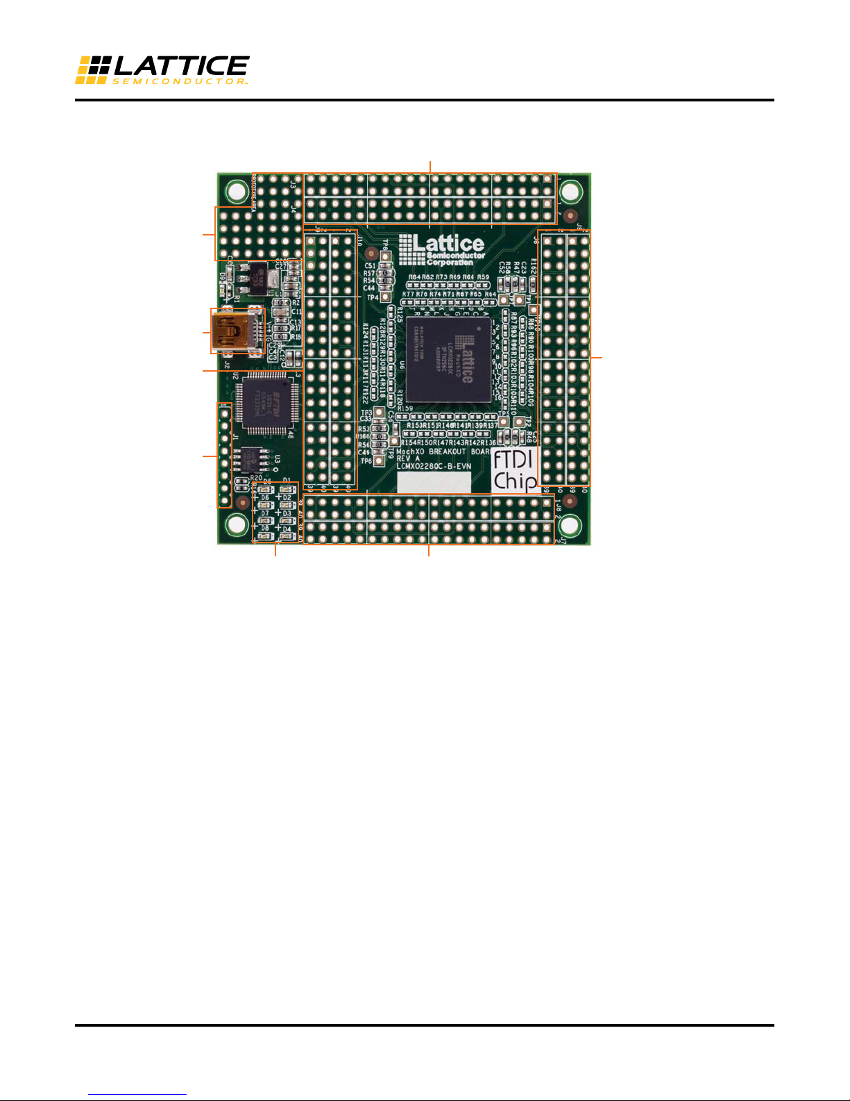
Figure 1. MachXO2280 Breakout Board, Top Side
Left Side
Two 2x20 Header
Landings (J9, J10)
USB
JTAG Header
Landing (J1)
LED
Array
Bottom Side
Two 2x20 Header Landings (J7 & J8)
Top Side
Two 2x20 Header Landings (J3 & J4 )
Right Side
Two 2x20 Header Landings
(J5 & J6)
Prototype
Area
MachXO2280 Breakout Board Evaluation Kit
Storage and Handling
Static electricity can shorten the lifespan of electronic components. Please observe these tips to prevent damage
that could occur from electro-static discharge:
• Use anti-static precautions such as operating on an an
• Store the evaluation board in the packaging provided.
• Touch a metal USB housing to equalize voltage potential between you and the board.
Software Requirements
You should install the following software before you begin developing new designs for the Breakout board:
• FTDI Chip USB Hardware Drivers
•
• ispVM System™ 17.9 or later (Required for re-programming)
MachXO2280 Device
This board features the MachXO2280 PLD which offers the benefits of increased system integration by providing
over 27Kbits of embedded memory, two built-in PLLs, high performance LVDS I/Os, and a low power sleep mode,
all in a single-device. The 256-pin ftBGA package provides 211 user I/Os in a 17mm x 17mm package. A complete
description of this device can be found in DS1002, MachXO Family Data Sheet.
ti-static mat and wearing an anti-static wrist-band.
Lattice Diamond™ (MachXO support)
3
Page 4
MachXO2280 Breakout Board Evaluation Kit
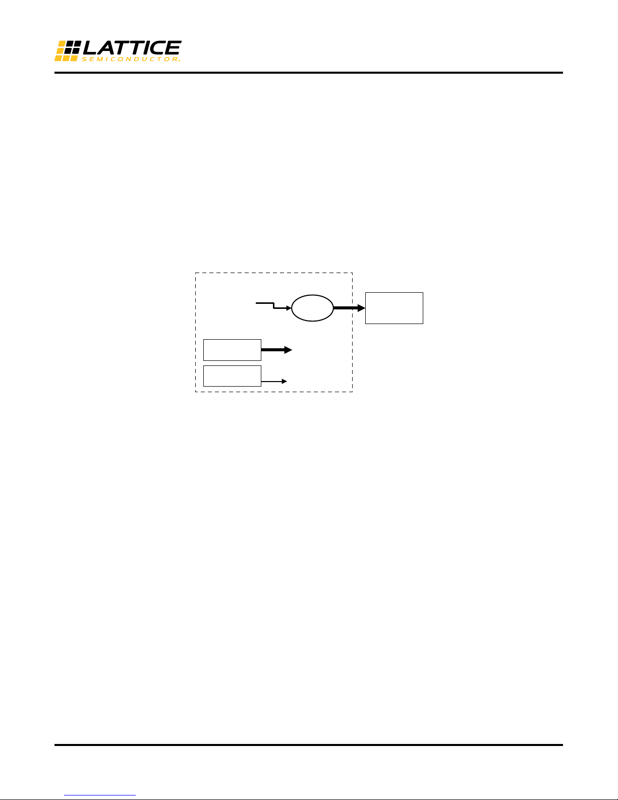
Demonstration Design
Lattice provides a pre-programmed demo to illustrate basic operation of the MachXO2280 device. The design integrates an up-counter with the on-chip
oscillator.
Note: You may obtain your Breakout Board after it has been
reprogrammed. To restore the factory default demo
and program it with other Lattice-supplied examples see the Download Demo Designs section of this document.
Run the Demonstration Design
The preprogrammed demonstration design is an up-counter to drive an LED array. The program shows a clock
generator based on the MachXO2280 on-chip oscillator. The counter module is clocked at ~22 MHz (18-26MHz) to
illustrate how low speed timer functions can be implemented with a PLD. The 23-bit up-counter further divides the
clock to advance the LED display approximately every 200ms. The resulting light pattern will appear as an alternating pair of lit LEDs per row.
Figure 2. Counter Demo Block Diagram
MachXO2280
c_delay[22]
(~0.5Hz)
23-bit
Up-Counter
Clock
Generator 18-26 MHz
c_delay[22:0]
WARNING: Do not connect the Breakout Board to your PC before you follow the driver installation procedure of
this section.
2x4 LED
Array
Communication with the Breakout Board with
a PC via the USB connection cable will require the FTDI chip USB
hardware drivers contained in the Software Requirements section. Loading these drivers enables the computer to
reliably recognize and program the Breakout Board. Drivers are distributed by Lattice as a stand-alone package or
h ispVM System version 17.9 or later. Use one of the two procedures below to install.
wit
To load the FTDI chip USB hardw
are drivers via ispVM System:
1. Browse to www.latticesemi.com/breakoutboards and download ispVM System software.
2. Install ispVM System software.
3. Run ispVM System. Choose is
The LSC 32/64-Bit USB Drivers Install/Uninstall dialog
4. Select FTDI U
SB 32-Bit Driver or FTDI USB 64-Bit Driver then click Install.
After a few moments, ispVM will indicate the installation is
5. Click OK, t
6. Choose Fil
hen click Close from the LSC 32/64-Bit USB Drivers Install/Uninstall dialog.
e > Exit to close ispVM System.
7. Connect the USB cable from a USB port on your PC to th
pTools > Install/Uninstall LSC USB/Parallel Port Driver.
appears.
complete.
e board’s USB mini-B socket (J2). After connection is
made, a green Power LED (D9) will light indicating the board is powered on.
8. Red LEDs will light and start to flash according to the preprog
rammed demonstration design.
See the Troubleshooting section of this guide if the board does not function as expected.
4
Page 5

MachXO2280 Breakout Board Evaluation Kit
To load the FTDI chip USB hardware drivers via the stand-alone package:
1. Browse to www.latticesemi.com/breakoutboards and download the FTDI chip USB Hardware driver package.
2. Extract the FTDI chip USB Hardware driver package to your PC hard drive.
3. Connect the USB cable from a USB port on your PC to the board’s USB mini-B socket (J2). After connection is
made, a green Power LED (D9) will light indicating the board is powered on.
4. If you are prompted, “Windows may connect to Windows Update” select No, not this time from available
options and click Next to proceed with the installation. Choose the Install from specific location (Advanced)
option and click Next.
5. Search for the best driver in these locations and click the Browse button to browse to the Windows driver folder
created in the Download Windows USB Hardware Drivers section. Select the CDM 2.04.06 WHQL Certified
folder and click OK.
6. Click Next. A screen will display as Windows copies the required driver files. Windows will display a message
indicating that the installation was successful.
7. Click Finish to install the USB driver.
8. Red LEDs will light and start to flash according to the preprogrammed demonstration design.
See the Troubleshooting section of this guide if the board does not function as expected.
Download Demo Designs
The counter demo is preprogrammed into the Breakout Board, however over time it is likely your board will be modified. Lattice distributes source and programming files for demonstration designs compatible with the Breakout
Board.
To download demo designs:
1. Browse to the Lattice Breakout Board Evaluation Kits web page (www.latticesemi.com/breakoutboards) of the
Lattice web site. Select MachXO Breakout Board Demo Source and save the file.
2. Extract the contents of MachXO2280_BB_Eval_Kit_v01.0.zip to an accessible location on your hard drive.
The demo design directory Demo_LED is unpacked.
Recompile a Demonstration Project with Lattice Diamond
Use the procedure described below to recompile a demo project for the Breakout Board.
1. Install and license Lattice Diamond software.
2. Download the demo source files from the Lattice Breakout Board Evaluation Kits web page.
3. Run Lattice Diamond.
4. Open the Demo_LED_OSC.ldf project file.
5. From the Process view, select JEDEC File from the Export Files process.
6. Choose Export Files, right-click and choose Run.
After a few moments the JEDEC programming file is output.
7. See section the Programming with ispVM section for details on downloading a programming file to the board.
5
Page 6

MachXO2280 Breakout Board Evaluation Kit
Programming with ispVM
A demonstration design is pre-programmed into the Breakout Board by Lattice. To restore a Breakout Board to factory settings or load an alternative demo design, use the procedures in this section.
To install ispVM programming tools:
1. Install and license ispVM System software.
2. Connect the board to a host PC using the USB port header connection.
3. Follow the USB Cable Interface procedure below to program the evaluation board.
The Breakout Board is equipped with a built-in USB-based programming circuit. This consists of a USB PHY and a
USB connector. When the board is connected to a PC with a USB cable, it is recognized by the ispVM System soft
ware as a USB Download Cable. The MachXO2280 can then be scanned and programmed using the ispVM System software.
To program a demo programming file:
1. From the Start menu run ispVM System.
ispVM appears.
2. Choose Options > Cable and IO Port Setup…
The Cable and I/O Port Setup dialog appears.
3. Make the following selections:
Cable Type: USB2
Port Setting: FTUSB-0
Click OK.
4. Choose ispTools > Scan Chain.
The New Scan Configuration Setup window appears. The LCMXO2280C device appears in the device list.
5. Right-click the LCMXO2280C entry and choose Edit Device…
The Device Information dialog appears.
6. From the Data File section, click the Browse button.
The Open Data File dialog appears.
7. Browse to the <Demo Dir> folder, select <Demo>.jed, and click Open. From the Operation list choose Erase,
Program, Verify and click OK.
8. Choose Project > Download.
ispVM reprograms the evaluation board.
Programming requires about 10 seconds. A small timer window will appear to show elapsed programming time. At
the end of programming, the configuration setup window should show a PASS in the Status column.
-
6
Page 7
MachXO2280 Breakout Board Evaluation Kit
LCMXO2280C
-3FTN256C
2x20 Header
Landing (J9)
LED
Array
GPIO
USB
Controller
USB Mini B
Socket
A/Mini-B
USB Cable
JTAG
Programming
8
2x20 Header
Landing (J10)
GPIO
2x20 Header
Landing (J5)
GPIO
2x20 Header
Landing (J6)
GPIO
1x8 JTAG Header
Landing (J1)
8
2x20 Header
Landing (J7)
2x20 Header
Landing (J8)
Bank 2,3
Bank 4,5
Bank 0,1
2x20 Header
Landing (J3)
2x20 Header
Landing (J4)
Bank 6,7
GPIOGPIO
GPIO GPIO
MachXO2280 Breakout Board
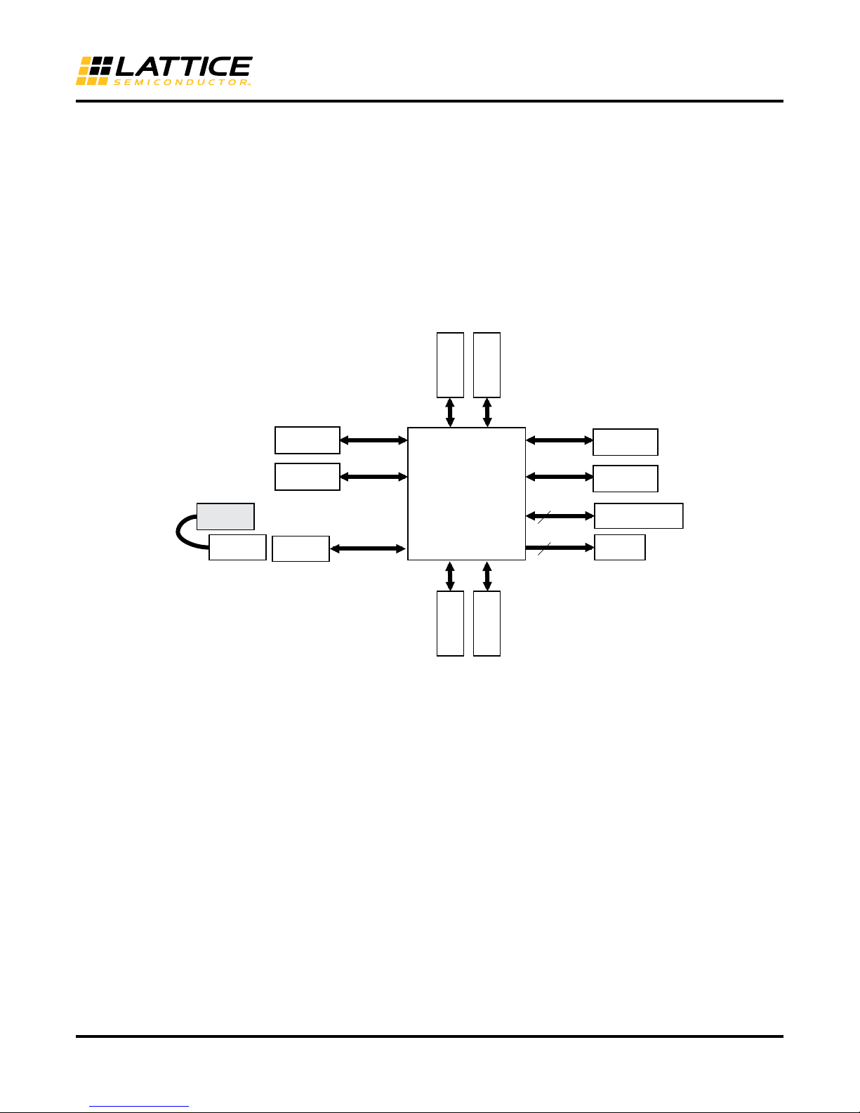
This section describes the features of the MachXO2280 Breakout Board in detail.
Overview
The Breakout Board is a complete development platform for the MachXO2280 PLD. The board includes a prototyping area, a USB program/power port, an LED array, and header land
PLD’s programmable I/O, power, and JTAG pins. The board is powered by the PC’s USB port or optionally with
external power. You may create or modify the program files using Diamond software and reprogram the board
using ispVM software.
Figure 3. MachXO2280 Breakout Board Block Diagram
ings with electrical connections to most of the
7
Page 8
MachXO2280 Breakout Board Evaluation Kit
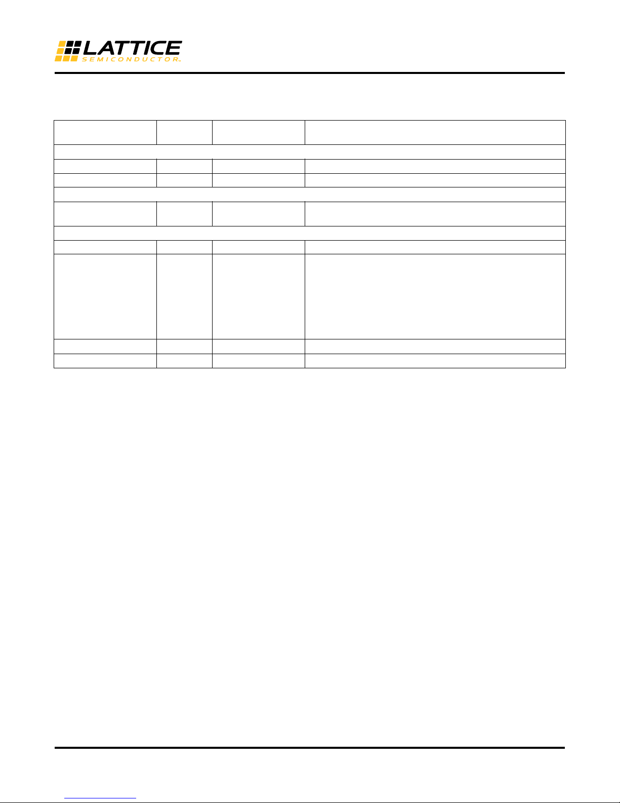
Ta bl e 1 describes the components on the board and the interfaces it supports.
Table 1. Breakout Board Components and Interfaces
Schematic
Component/Interface Type
Circuits
USB Controller Circuit U2: FT2232H USB-to-JTAG interface and dual USB UART/FIFO IC
USB Mini-B Socket I/O J1:USB_MINI_B Programming and debug interface
Components
LCMXO2280C PLD
Interfaces
LED Array Output D8-D1 Red LEDs
Eight 2x20 Header
Landings
1x8 Header Landing I/O J1: header_1x8 Optional JTAG interface
4-Hole Prototype Area Prototype area 100mil centered holes.
I/O
Reference Description
U4: LCMXO2280C3
FTN256C
J3: header_2x20
J4: header_2x20
J5: header_2x20
J6: header_2x20
J7: header_2x20
J8: header_2x20
J9: header_2x20
J10: header_2x20
2280-LUT device packaged in a 17 x 17mm, 256-ball ftBGA.
User-definable I/O
8
Page 9
MachXO2280 Breakout Board Evaluation Kit
Subsystems
This section describes the principle sub systems for the Breakout Board in alphabetical order.
Clock Sources
All clocks for the counter demonstration designs originate from the
use an expansion header landing to drive a PLD input with an external clock source.
Expansion Header Landings
The expansion header landings provide access to user GPIOs, primary inputs, clocks, and VCCO pins of the
Ma
chXO2280. The remaining pins serve as power supplies for external connections. Each landing is configured as
one 2x20 100 mil.
Table 2. Expansion Connector Reference
Item Description
Reference Designators J3, J4, J5, J6, J7, J8, J9, J10
Part Number header_2x20
Table 3. Expansion Header Pin Information (J3)
Pin Number Function MachXO2280 Ball
1 PL2A_LV_T E4
2 PL11A_LV_T H2
3 PL2B_LV_T E5
4 PL11B_LV_C J2
5 GND n/a
6 GND n/a
7 PL3A_LV_T F5
8 PL12A_LV_T J1
9 PL3B_LV_C F6
10 PL12B_LV_C K1
11 GND n/a
12 GND n/a
13 PL4A_LV_T E3
14 PL13A_LV_T L1
15 PL4B_LV_C E2
16 PL13B_LV_C M1
17 GND n/a
18 GND n/a
19 PL5A_LV_T B1
20 PL15A_LV_T L3
21 PL5B_LV_C C1
22 PL15B_LV_C M3
23 GND n/a
24 GND n/a
25 PL7A_LV_T F2
26 PL16A_LV_T J4
27 PL7B_LV_C G2
28 PL16B_LV_C J5
MachXO2280 PLD on-chip oscillator. You may
9
Page 10
MachXO2280 Breakout Board Evaluation Kit
Pin Number Function MachXO2280 Ball
29 GND n/a
30 GND n/a
31 PL8A_LV_T G4
32 PL17A_LV_T K5
33 PL8B_LV_C G5
34 PL17B_LV_C K4
35 GND n/a
36 GND n/a
37 PL9A_LV_T H4
38 PL18A_LV_T M5
39 PL9B_LV_C H5
40 PL18B_LV_C M4
10
Page 11

Table 4. Expansion Header Pin Information (J4)
Pin Number Function MachXO2280 Ball
1 PL3C F3
2 GND n/a
3 PL3D F4
4 GND n/a
5 PL4C C3
6 GND n/a
7 PL4D C2
8 GND n/a
9 PL6C D2
10 GND n/a
11 PL6D D1
12 GND n/a
13 PL7C E1
14 GND n/a
15 PL7D F1
16 GND n/a
17 PL8C G3
18 GND n/a
19 PL8D H3
20 GND n/a
21 PL10C G1
22 GND n/a
23 PL10D H1
24 GND n/a
25 NC NC
26 PL15C M2
27 NC NC
28 PL15D N2
29 PL11C J3
30 PL16C R1
31 PL11D K3
32 PL16D R2
33 PL12C K2
34 PL17C L5
35 PL12D L2
36 PL17D L4
37 PL14C N1
38 PL19A N4
39 PL14D P1
40 PL19B N3
MachXO2280 Breakout Board Evaluation Kit
11
Page 12

Table 5. Expansion Header Pin Information (J5)
Pin Number Function MachXO2280 Ball
1 PT2C B2
2 PT9A D8
3 PT2D B3
4 PT9C E8
5 PT3A A2
6 PT9D E9
7 PT3B A3
8 PT10A A10
9 PT3C D3
10 PT10C C9
11 PT3D D4
12 PT10D C10
13 PT4A C4
14 PT10E D9
15 PT4B C5
16 PT10F D10
17 PT5A D6
18 PT11A B9
19 PT5B D5
20 PT11B B10
21 PT5C B4
22 PT12A A11
23 PT5D B5
24 PT12B A12
25 PT6E E7
26 PT12C B11
27 PT6F E6
28 PT12D B12
29 PT6C A5
30 PT13C C11
31 PT6D A4
32 PT13D C12
33 PT6A C6
34 PT14A A13
35 PT6B C7
36 PT14B A14
37 PT7A B6
38 PT14C D11
39 PT7B B7
40 PT14D D12
MachXO2280 Breakout Board Evaluation Kit
12
Page 13

Table 6. Expansion Header Pin Information (J6)
Pin Number Function MachXO2280 Ball
1 VCIO_extB7 G6
2 GND n/a
3 VCIO_extB6 J6
4 GND n/a
5 VCIO_extB5 L7
6 GND n/a
7 VCIO_extB4 L9
8 GND n/a
9 VCIO_extB3 J11
10 GND n/a
11 VCIO_extB2 G11
12 GND n/a
13 VCIO_extB1 F9
14 GND n/a
15 VCIO_extB0 F7
16 GND n/a
17 NC NC
18 NC NC
19 NC NC
20 NC NC
21 NC NC
22 PT15A E10
23 NC NC
24 PT15B E11
25 NC NC
26 PT15C B13
27 NC NC
28 PT15D C13
29 PT7C A6
30 PT16A B14
31 PT7D A7
32 PT16B C14
33 PT8C B8
34 PT16C A15
35 PT8D C8
36 PT16D B15
37 NC NC
38 GND n/a
39 NC NC
40 GND n/a
MachXO2280 Breakout Board Evaluation Kit
13
Page 14

Table 7. Expansion Header Pin Information (J7)
Pin Number Function LCMXO2280C Ball
1 PR4C F13
2 GND n/a
3 PR4D F12
4 GND n/a
5 PR5C B16
6 GND n/a
7 PR5D C16
8 GND n/a
9 PR6C D16
10 GND n/a
11 PR6D E16
12 GND n/a
13 PR7C F16
14 GND n/a
15 PR7D G16
16 GND n/a
17 PR9C H12
18 GND n/a
19 PR9D H13
20 GND n/a
21 PR10C G15
22 GND n/a
23 PR10D H15
24 GND n/a
25 NC NC
26 PR15C M16
27 NC NC
28 PR15D N16
29 PR11C J12
30 PR16C L12
31 PR11D K12
32 PR16D L13
33 PR13C J14
34 PR17C M12
35 PR13D K14
36 PR17D M13
37 PR14C K16
38 PR20A L11
39 PR14D L16
40 PR20B M11
MachXO2280 Breakout Board Evaluation Kit
14
Page 15

Table 8. Expansion Header Pin Information (J8)
Pin Number Function MachXO2280 Ball
1 PR3A_LV_T D14
2 PR11A_LV_T H16
3 PR3B_LV_C D13
4 PR11B_LV_C J16
5 GND n/a
6 GND n/a
7 PR4A_LV_T E13
8 PR13A_LV_T J15
9 PR4B_LV_C E12
10 PR13B_LV_C K15
11 GND n/a
12 GND n/a
13 PR5A_LV_T E14
14 PR14A_LV_T J13
15 PR5B_LV_C F14
16 PR14B_LV_C K13
17 GND n/a
18 GND n/a
19 PR6A_LV_T C15
20 PR15A_LV_T L15
21 PR6B_LV_C D15
22 PR15B_LV_C M15
23 GND n/a
24 GND n/a
25 PR7A_LV_T E14
26 PR16A_LV_T L14
27 PR7B_LV_C F15
28 PR16B_LV_C M14
29 GND n/a
30 GND n/a
31 PR9A_LV_T G12
32 PR17A_LV_T N15
33 PR9B_LV_C G13
34 PR17B_LV_C N14
35 GND n/a
36 GND n/a
37 PR10A_LV_T G14
38 PR18A_LV_T N13
39 PR10B_LV_C H14
40 PR18B_LV_C N12
MachXO2280 Breakout Board Evaluation Kit
15
Page 16

Table 9. Expansion Header Pin Information (J9)
Pin Number Function MachXO2280 Ball
1 VCC_3.3V n/a
2 GND n/a
3 VCC_3.3V n/a
4 GND n/a
5 VCC_3.3V n/a
6 GND n/a
7 NC NC
8 GND n/a
9 NC NC
10 VCC_CORE n/a
11 CLK0 (PT9B) D7
12 GND n/a
13 CLK1 (PT10B) A9
14 GND n/a
15 CLK2 (PB10F) N9
16 GND n/a
17 CLK3 (PB10B) M9
18 GND n/a
19 NC NC
20 NC NC
21 NC NC
22 NC NC
23 SLEEPN P13
24 GND n/a
25 PB14D R14
26 GND n/a
27 PB15A T14
28 GND n/a
29 PB15B T15
30 GND n/a
31 PB15D P14
32 GND n/a
33 PB16A R15
34 GND n/a
35 PB16B R16
36 GND n/a
37 PB16C P15
38 GND n/a
39 PB16D P16
40 GND n/a
MachXO2280 Breakout Board Evaluation Kit
16
Page 17

Table 10. Expansion Header Pin Information (J10)
Pin Number Function MachXO2280 Ball
1 PB9B P8
2 PB2A P2
3 PB9A P7
4 PB2B P3
5 PB10E N8
6 PB2C N5
7 PB10C P9
8 PB2D N6
9 PB10D P10
10 PB3A T2
11 PB10A M10
12 PB3B T3
13 PB11C R9
14 PB3C R4
15 PB11D R10
16 PB3D R5
17 PB12A T10
18 PB4A P5
19 PB12B T11
20 PB4B P6
21 PB12C N10
22 PB4C T5
23 PB12D N11
24 PB4D T4
25 PB13A R11
26 PB5A R6
27 PB13B R12
28 PB5B T6
29 PB13C P11
30 PB6A T8
31 PB13D P12
32 PB6B T7
33 PB14A T13
34 PB7C M7
35 PB14B T12
36 PB7D M8
37 PB14C R13
38 PB8C R7
39 NC NC
40 PB8D R8
MachXO2280 Breakout Board Evaluation Kit
17
Page 18

Figure 4. J3/J4 Header Landing Callout
1
E4
E5
GND
F5
F6
GND
E3
E2
GND
B1
C1
GND
F2
G2
GND
G4
G5
GND
H4
H5
39
2
H2
J2
GND
J1
K1
GND
L1
M1
GND
L3
M3
GND
J4
J5
GND
K5
K4
GND
M5
M4
40
1
F3
F4
C3
C2
D2
D1
E1
F1
G3
H3
G1
H1
NC
NC
J3
K3
K2
L2
N1
PI
39
2
GND
GND
GND
GND
GND
GND
GND
GND
GND
GND
GND
GND
M2
N2
R1
R2
L5
L4
N4
N3
40
J3
J4
J3
J4
Top Side
J6 J5
Top Side
1
G6
J6
L7
L9
J11
G11
F9
F7
NC
NC
NC
NC
NC
NC
A6
A7
B8
C8
NC
NC
39
2
GND
GND
GND
GND
GND
GND
GND
GND
NC
NC
E10
E11
B13
C13
B14
C14
A15
B15
GND
GND
40
1
B2
B3
A2
A3
D3
D4
C4
C5
D6
D5
B4
B5
E7
E6
A5
A4
C6
C7
B6
B7
39
2
D8
E8
E9
A10
C9
C10
D9
D10
B9
B10
A11
A12
B11
B12
C11
C12
A13
A14
D11
D12
40
J6
J5
MachXO2280 Breakout Board Evaluation Kit
Figure 5. J5/J6 Header Landing Callout
18
Page 19

Figure 6. J7/J8 Header Landing Callout
J8
J7
Top Side
1
D14
D13
GND
E13
E12
GND
E14
F14
GND
C15
D15
GND
E14
F15
GND
G12
G13
GND
G14
H14
39
2
H16
J16
GND
J15
K15
GND
J13
K13
GND
L15
M15
GND
L14
M14
GND
N15
N14
GND
N13
N12
40
1
F13
F12
B16
C16
D16
E16
F16
G16
H12
H13
G15
H15
NC
NC
J12
K12
J14
K14
K16
L16
39
2
GND
GND
GND
GND
GND
GND
GND
GND
GND
GND
GND
GND
M16
N16
L12
L13
M12
M13
L11
M11
40
J8
J7
MachXO2280 Breakout Board Evaluation Kit
Figure 7. J9/J10 Header Landing Callout
J10
1
P8
P7
N8
P9
P10
M10
R9
R10
T10
T11
N10
N11
R11
R12
P11
P12
T13
T12
R13
NC
39
1
VCC_3.3 V
VCC_3.3 V
VCC_3.3 V
NC
NC
D7
A9
N9
M9
NC
NC
P13
R14
T14
T15
P14
R15
R16
P15
P16
39
J9
2
GND
GND
GND
VCC_CORE
GND
GND
GND
GND
GND
NC
NC
GND
GND
GND
GND
GND
GND
GND
GND
GND
40
P2
P3
N5
N6
T2
T3
R4
R5
P5
P6
T5
T4
R6
T6
T8
T7
M7
M8
R7
R8
40
Top Side
2
J9 J10
19
Page 20

Figure 8. J1 Header Landing and LED Array Callout
Top Side
MachXO2280 Breakout Board Evaluation Kit
1
VCC3FT
NC
NC
TCK
TDI
TDO
TMS
GND
8
J1
LED
J9
D5
IO_18
IO_16
IO_14
IO_12
D8
D1
IO_J12
IO_J10
IO_I12
IO_I10
D4
MachXO2280 PLD
The LCMXO2280C-3FTN256C is a 256-ball BGA package PLD device which provides 211 I/Os in a 17 x 17mm
ackage.
p
Table 11. MachXO PLD Interface Reference
Item Description
Reference Designators U4
Part Number LCMXO2280C-3FTN256C
Manufacturer Lattice Semiconductor
Web Site www.latticesemi.com
JTAG Interface Circuits
For power and programming an FTDI USB UART/FIFO IC converter provides a communication interface between a
st and the JTAG programming chain of the Breakout Board. The USB 5V supply is also used as a source for
PC ho
the 3.3V supply rail. A USB mini-B socket is provided for the USB connector cable.
20
Page 21

Table 12. JTAG Interface Reference
Item Description
Reference Designators U2
Part Number FT2232HL
Manufacturer Future Technology Devices International (FTDI)
Web Site
www.ftdichip.com
Table 13. JTAG Programming Pin Information
Description MachXO2280 Pin
Test Data Output 107:TDO
Test Data Input 2:TDI
Test Mode Select 74:TMS
Test Clock 35:TCK
LEDs
A green LED (D9) is used to indicate USB 5V power. Eig
device.
Table 14. Power and User LEDs Reference
MachXO2280 Breakout Board Evaluation Kit
ht red LEDs are driven by I/O pins of the MachXO2280
Item Description
Reference Designators
Part Number
Manufacturer Lite-On It Corporation
Web Site
D1, D2, D3, D4, D5, D6, D7,
D8
, D9
LTST-C190KRKT (D1-D8)
LTST-C190KGKT (D9)
www.liteonit.com
Power Supply
3.3V supply rail is converted from the USB 5V interf
ace when the board is connected to a host PC.
Test Points
In order to check the various voltage levels used, test points are provided:
• TP1, VCC3D (VCCIO Bank 0)
•
TP2, VCC3D (VCCIO Bank 1)
• TP3, VCC3D (VCCIO Bank 4)
• TP4, VCC3D (VCCIO Bank 5)
• TP5, VCC3D (VCCIO Bank 2)
• TP6, VCC3D (VCCIO Bank 3)
• TP7, VCC3D (VCCIO Bank 7)
• TP8, VCC3D (VCCIO Bank 6)
• TP9, VCC3D (VCC Core)
• TP10, VCC3D (VCCAUX)
21
Page 22

MachXO2280 Breakout Board Evaluation Kit
USB Programming and Debug Interface
The USB mini-B socket of the Breakout Board serves as the programming and debug interface.
JTAG Programming: For JTAG programming, a preprogrammed USB PHY peripheral controller is provided on the
Breakout Board to serve as the programming interface to the MachXO2280 PLD.
Programming requires the ispVM System software.
Table 15. USB Interface Reference
Item Description
Reference Designators U2
Part Number FT2232HL
Manufacturer Future Technology Devices International (FTDI)
Web Site www.ftdichip.com
Board Modifications
This section describes modifications to the board to change or add functionality.
Bypassing the USB Programmin
The USB programming interface circuit (USB Programming and Debug Interface section) may be optionally
bypassed by removing the 0 ohm resistors: R3, R4, R7, and R9 (See Appendix A. Schematics, Sheet 2 of 5).
Header landing J1 provides JTAG signal access for jumper wires or a 1x8 pin header.
Applying External Power
The Breakout Board is powered by the circuit of Schemat
may disconnect this power source by removing the 0 ohm resistors: R47 (VCCIO 3.3V, Bank 0), R48 (VCCIO 3.3V,
Bank 1), R53 (VCCIO 3.3V, Bank 4), R54 (VCCIO 3.3V, Bank 5), R55 (VCCIO 3.3V, Bank 2), R56 (VCCIO 3.3V,
Bank 3), R57 (VCCIO 3.3V, Bank 6), R58 (VCCIO 3.3V, Bank 7), R160 (VCC core) and R162 (VCCAUX). Power
connections are available from the expansion header landing, J9, Schematic Sheet 3 of 5.
Measuring Bank and Core Voltages
Test points (TP1, through TP10) provide access to power supplies of the MachXO2280 PLD. 0 ohm resistors: R47
VCCIO 3.3V, Bank 0), R48 (VCCIO 3.3V, Bank 1), R53 (VCCIO 3.3V, Bank 4), R54 (VCCIO 3.3V, Bank 5), R55
(
(VCCIO 3.3V, Bank 2), R56 (VCCIO 3.3V, Bank 3), R57 (VCCIO 3.3V, Bank 6), R58 (VCCIO 3.3V, Bank 7), R160
(VCC core) and R162 (VCCAUX)can be removed to add a current meter inline or add a resistor shunt to measure
voltage across.
g Interface
ic Sheet 2 of 4 based on the 5V USB power source. You
Mechanical Specifications
Dimensions: 3 in. [L] x 3 in. [W] x 1/2 in. [H]
Environmental Requirements
The evaluation board must be stored between -40° C and 100° C. The recommended operating temperature is
between 0° C and 90° C.
The board can be damaged without proper anti-static handling.
22
Page 23

MachXO2280 Breakout Board Evaluation Kit
Glossary
PLD: Programmable Logic Device
DIP: Dual in-line package
LED: Light Emitting Diode.
LUT: Look Up Table
PCB: Printed Circuit Board
RoHS: Restriction of Hazardous Substances Directive
USB: Universal Serial Bus
WDT: Watchdog Timer
Troubleshooting
Use the tips in this section to diagnose problems with the Breakout Board.
LEDs Do Not Flash
If power is applied but the board does not flash according to the preprogrammed counter demonstration then it is
likely the board has been reprogrammed with a new design. Follow the directions in the
tion to restore the factory default.
Demonstration Design sec-
USB Cable Not Detected
If ispVM System does not recognize the USB cable even after installing the Lattice USB port drivers and rebooting,
the incorrect USB driver may have been installed. This usually occurs if you attach the board to your PC prior to
installing the USB driver or ispVM System software.
To access the Troubleshooting the USB Driver Installation Guide:
1. Start ispVM System and choose Options > Cable and I/O Port Setup.
The Cable and I/O Port Setup Dialog appears.
2. Click the Troubleshooting the USB Driver Installation Guide link.
The Troubleshooting the USB Driver Installation Guide document appears in your system’s PDF file reader.
3. Follow the directions of the guide to install the Lattice USB driver.
Determine the Source of a Pre-Programmed Device
You may receive your Breakout Board after it has been reprogrammed by someone else. To restore the board to
the factory default, see the
device.
You can also determine which demo design is currently programmed onto the Breakout Board by comparing the
JEDEC checksums against of the programming file with what is read from the programmed device.
To compare JEDEC file checksum:
1. Connect the Breakout Board to a host PC using the USB port.
Download Demo Designs section for details on downloading and reprogramming the
2. Start ispVM and choose ispTools > Scan.
The device appears in the Device List.
3. Double-click the device row.
The Device Information dialog appears.
23
Page 24

MachXO2280 Breakout Board Evaluation Kit
4. Click the Browse button.
The Save as Data File dialog appears.
5. Specify a new JEDEC Data File name and clic
6. From the Op
7. Choose Pr
ispVM reads the contents from the device and writes the results to the JEDEC file specified.
Open the JEDEC file into a text editor and page to the bottom of the file.
Note the hexidecimal checksum at the line above the User Electronic Data note line. Compare this value
a
gainst the checksum of the original JEDEC demo programming files.
Lattice Diamond Programmer Error
Lattice Diamond 1.1 reports “File not valid error” from the Programmer interface.
Diamond 1.1 is not Programmer compatible with the MachXO2280 Breakout Board. To program the device, use
isp
VM System 17.9 or later.
eration list choose Read and Save JEDEC and click OK.
oject > Download.
k the Save button.
Ordering Information
China RoHS Environment-Friendly
Description Ordering Part Number
se Period (EFUP)
U
MachXO2280 Breakout Board Evaluation Kit LCMXO2280C-B-EVN
Technical Support Assistance
e-mail: techsupport@latticesemi.com
Internet: www
.latticesemi.com
Revision History
Date Version Change Summary
February 2015 1.1
March 2011 01.0
© 2015 Lattice Semiconductor Corp. All Lattice trademarks, registered trademarks, patents, and disclaimers are as
listed at www.latticesemi.com/legal. All o
their respective holders. The specificat
ther brand or product names are trademarks or registered trademarks of
ions and information herein are subject to change without notice.
Updated Subsystems section. Revised the following figures:
— Figure 4, J3/J4 Header Landing Callout
— Figure 5, J5/J6 Header Landing Callout
— Figure 6, J7/J8 Header Landing Callout
— Figure 7, J9/J10 Header Landing Callout
Updated Technical Support Assistance information.
Updated corporate logo.
Initial release.
24
Page 25

Appendix A. Schematics
5
5
4
4
3
3
2
2
1
1
D
D
C C
B
B
A A
Title
veRrebmuN tnemucoDeziS
teehS:etaD
of
AXELSYS
LCMXO2280C-B-EVN
A
MachXO Breakout Board, Cover
B
15Thursday, December 30, 2010
Title
veRrebmuN tnemucoDeziS
teehS:etaD
of
AXELSYS
LCMXO2280C-B-EVN
A
MachXO Breakout Board, Cover
B
15Thursday, December 30, 2010
Title
veRrebmuN tnemucoDeziS
teehS:etaD
of
AXELSYS
LCMXO2280C-B-EVN
A
MachXO Breakout Board, Cover
B
15Thursday, December 30, 2010
USB CON
USB to JTAG
MACHXO
LED ARRAY
CONNECTED HEADER
CONNECTED HEADER
PROTOTYPE AREA
Resistant Tolerance: R12 1%
All the rest up to 5%
Figure 9. MachXO2280 Breakout Board
MachXO2280 Breakout Board Evaluation Kit
25
Page 26

Figure 10. USB Interface to JTAG
5
5
4
4
3
3
2
2
1
1
D D
C C
B B
A
A
Dm
Dp
FT_EECS
FT_EECLK
FT_EEDATA
FT_EEDATA
TMS
TDI
TDO
TCK
TCK
TDI
TDO
TMS
FT_EECS
FT_EECLK
VCC3FT
VBUS_5V
VCC_3.3V
VBUS_5V
VCC3D
VCC3FT
VCC3FT
VCC3FT
VCC1_8FT
VCC3FTVCC1_8FT
VCC3FT
VCC3FT
VCC3FT
TCK (4)
TDI (4)
TDO (4)
TMS (4)
Title
veRrebmuN tnemucoDeziS
teehS:etaD
of
AXELSYS
LCMXO2280C-B-EVN
A
MachXO Breakout Board, USBIF to JTAG
C
25Thursday, December 30, 2010
Title
veRrebmuN tnemucoDeziS
teehS:etaD
of
AXELSYS
LCMXO2280C-B-EVN
A
MachXO Breakout Board, USBIF to JTAG
C
25Thursday, December 30, 2010
Title
veRrebmuN tnemucoDeziS
teehS:etaD
of
AXELSYS
LCMXO2280C-B-EVN
A
MachXO Breakout Board, USBIF to JTAG
C
25Thursday, December 30, 2010
Default
21
R12 12k 1%R12 12k 1%
12
C11
22u
C11
22u
2 1
R20
5k1
R20
5k1
21
R170 R170
12
C8
0.1uF
cc0402C80.1uF
cc0402
21
R1 1kR1 1k
1
1
3
3
G1
2
G2
4
X1
12MHZX112MHZ
12
C21
0.1uF
C21
0.1uF
12
C7
0.1uF
cc0402C70.1uF
cc0402
1 2
C18
18pF
C18
18pF
CS
1
CLK2DI3DO
4
VSS
5
ORG
6
NU
7
VCC
8
93LC56-SO8U393LC56-SO8
U3
12
C4
0.1uFC40.1uF
12
C6
0.1uF
cc0402C60.1uF
cc0402
2 1
R14
5k1
R14
5k1
12
C5
0.1uF
cc0402C50.1uF
cc0402
21
R70 R70
2
1
R40 R4021R30 R3021R90 R90
2
1
R190 R190
1 2
C200.1uF C200.1uF
12
C10
10u
C10
10u
12
D9
GreenD9Green
2 1
R16
5k1
R16
5k1
21
R115k1 R115k1
12
L4
600ohm 500mAL4600ohm 500mA
12
C16
10u
C16
10u
12
C12
4u7
C12
4u7
2 1
R21
10k
R21
10k
12
C17
0.1uF
C17
0.1uF
12
C15
0.1uF
C15
0.1uF
VREGIN50VREGOUT49DM7DP8REF
6
RESET#
14
EECS
63
EECLK
62
EEDATA61OSCI
2
OSCO
3
TEST
13
ADBUS016ADBUS1
17
ADBUS218ADBUS3
19
VPHY
4
VPLL
9
VCORE
12
VCORE
37
VCORE
64
VCCIO
20
VCCIO
31
VCCIO
42
VCCIO
56
AGND
10
GND
1
GND
5
GND
11
GND
15
GND
25
GND
35
GND
47
GND
51
PWREN#
60
SUSPEND#
36
ADBUS421ADBUS522ADBUS6
23
ADBUS7
24
ACBUS0
26
ACBUS127ACBUS228ACBUS3
29
ACBUS430ACBUS5
32
ACBUS633ACBUS734BDBUS0
38
BDBUS139BDBUS240BDBUS3
41
BDBUS4
43
BDBUS5
44
BDBUS645BDBUS746BCBUS0
48
BCBUS152BCBUS2
53
BCBUS3
54
BCBUS4
55
BCBUS557BCBUS658BCBUS7
59
FTDI High-Speed USB
FT2232H
FT2232HL
U2
FTDI High-Speed USB
FT2232H
FT2232HL
U2
VCC
1
D-
2
D+
3
ID
4
GND
5
J2
SKT_MINIUSB_B_RA
J2
SKT_MINIUSB_B_RA
21
R20 R20
21
R22 2k2R22 2k2
12
L3
600ohm 500mAL3600ohm 500mA
GND
1
IN
3
OUT
2
TAB
4
U1
NCP1117ST33U1NCP1117ST33
1
1
2
2
3
3
445566778
8
J1
header_1x8
DNI
J1
header_1x8
DNI
2 1
R15
5k1
R15
5k1
12
C3
4u7C34u7
12
C13
0.1uF
C13
0.1uF
2
1
R180 R180
1 2
C19
18pF
C19
18pF
12
C9
0.1uF
cc0402C90.1uF
cc0402
12
C14
0.1uF
C14
0.1uF
12
L1
600ohm 500mAL1600ohm 500mA
MachXO2280 Breakout Board Evaluation Kit
26
Page 27

Figure 11. Connectors and LEDs
5
5
4
4
3
3
2
2
1
1
D D
C C
B B
A
A
VCC_3.3V
VCC3D
CLK0(4)
CLK1(4)
CLK2(4)
CLK3(4)
PR3A_LV_T(5)
PR3B_LV_C(5)
PR4A_LV_T(5)
PR4B_LV_C(5)
PR5A_LV_T(5)
PR5B_LV_C(5)
PR6A_LV_T(5)
PR6B_LV_C(5)
PR7A_LV_T(5)
PR7B_LV_C(5)
PR9A_LV_T(5)
PR9B_LV_C(5)
PR10A_LV_T(5)
PR10B_LV_C(5)
PR13A_LV_T (5)
PR13B_LV_C (5)
PR14A_LV_T (5)
PR14B_LV_C (5)
PR15A_LV_T (5)
PR15B_LV_C (5)
PR11A_LV_T (5)
PR16A_LV_T (5)
PR16B_LV_C (5)
PR17A_LV_T (5)
PR17B_LV_C (5)
PR18A_LV_T (5)
PR18B_LV_C (5)
PR11B_LV_C (5)
PL3A_LV_T(4)
PL3B_LV_C(4)
PL4A_LV_T(4)
PL4B_LV_C(4)
PL5A_LV_T(4)
PL5B_LV_C(4)
PL7A_LV_T(4)
PL7B_LV_C(4)
PL8A_LV_T(4)
PL8B_LV_C(4)
PL9A_LV_T(4)
PL9B_LV_C(4)
PL2A_LV_T(4)
PL2B_LV_C(4)
PL18A_LV_T (4)
PL18B_LV_C (4)
PL11A_LV_T (4)
PL11B_LV_C (4)
PL12A_LV_T (4)
PL12B_LV_C (4)
PL13A_LV_T (4)
PL13B_LV_C (4)
PL15A_LV_T (4)
PL15B_LV_C (4)
PL16A_LV_T (4)
PL16B_LV_C (4)
PL17A_LV_T (4)
PL17B_LV_C (4)
PR4C(5)
PR4D(5)
PR5C(5)
PR5D(5)
PR6C(5)
PR6D(5)
PR7C(5)
PR7D(5)
PR9C(5)
PR9D(5)
PR10C(5)
PR10D(5)
PR11C(5)
PR11D(5)
PR13C(5)
PR13D(5)
PR14C(5)
PR14D(5)
PR15C (5)
PR15D (5)
PR16C (5)
PR16D (5)
PR17C (5)
PR17D (5)
PR20A (5)
PR20B (5)
PL3C(4)
PL3D(4)
PL4C(4)
PL4D(4)
PL6C(4)
PL6D(4)
PL7C(4)
PL7D(4)
PL8C(4)
PL8D(4)
PL10C(4)
PL10D(4)
PL19A (4)
PL19B (4)
PL11C(4)
PL11D(4)
PL12C(4)
PL12D(4)
PL14C(4)
PL14D(4)
PL15C (4)
PL15D (4)
PL16C (4)
PL16D (4)
PL17C (4)
PL17D (4)
PT2C(4)
PT2D(4)
PT3A(4)
PT3B(4)
PT3C(4)
PT3D(4)
PT4A(4)
PT4B(4)
PT5A(4)
PT5B(4)
PT5C(4)
PT5D(4)
PT6E(4)
PT6F(4)
PT6C(4)
PT6D(4)
PT6A(4)
PT6B(4)
PT7A(4)
PT7B(4)
PT7C(4)
PT7D(4)
PT8C(4)
PT8D(4)
PT9A (4)
PT9C (4)
PT9D (4)
PT10A (4)
PT10C (4)
PT10D (4)
PT10E (4)
PT10F (4)
PT11A (4)
PT11B (4)
PT12A (4)
PT12B (4)
PT12C (4)
PT12D (4)
PT13C (4)
PT13D (4)
PT14A (4)
PT14B (4)
PT14C (4)
PT14D (4)
PT15A (4)
PT15B (4)
PT15C (4)
PT15D (4)
PT16A (4)
PT16B (4)
PT16C (4)
PT16D (4)
PB9A(4)
PB10E(4)
PB10C(4)
PB10A(4)
PB11C(4)
PB11D(4)
PB12A(4)
PB12B(4)
PB12C(4)
PB12D(4)
PB13A(4)
PB13B(4)
PB13C(4)
PB13D(4)
PB14A(4)
PB14B(4)
PB14C(4)
PB15A(4)
PB15B(4)
SLEEPN#(4)
PB15D(4)
PB16A(4)
PB16B(4)
PB16C(4)
PB16D(4)
PB9B(4)
PB10D(4)
PB14D(4)
PB2A (4)
PB2B (4)
PB2C (4)
PB2D (4)
PB3A (4)
PB3B (4)
PB3C (4)
PB3D (4)
PB4A (4)
PB4B (4)
PB4C (4)
PB4D (4)
PB5A (4)
PB5B (4)
PB6A (4)
PB6B (4)
PB7C (4)
PB7D (4)
PB8C (4)
PB8D (4)
PB15A(4)
PB15B(4)
PB15D(4)
PB16A(4)
PB16B(4)
PB16C(4)
PB16D(4)
PB14D(4)
VCC_CORE (4,5)
VCIO_extB7(5)
VCIO_extB0(5)
VCIO_extB6(5)
VCIO_extB1(5)
VCIO_extB5(5)
VCIO_extB2(5)
VCIO_extB4(5)
VCIO_extB3(5)
Title
veRrebmuN tnemucoDeziS
teehS:etaD
of
AXELSYS
LCMXO2280C-B-EVN
A
MachXO Breakout Board, CON and LED
C
35Thursday, December 30, 2010
Title
veRrebmuN tnemucoDeziS
teehS:etaD
of
AXELSYS
LCMXO2280C-B-EVN
A
MachXO Breakout Board, CON and LED
C
35Thursday, December 30, 2010
Title
veRrebmuN tnemucoDeziS
teehS:etaD
of
AXELSYS
LCMXO2280C-B-EVN
A
MachXO Breakout Board, CON and LED
C
35Thursday, December 30, 2010
3X15 PROTOTYPE AREA
LED DISPLAY ARRAY
EXTERNAL POWER PINS
5knaB,4knaB1knaB,0knaB6knaB,7knaB3knaB,2knaB
2 1
R46
470
R46
470
12
D7
RedD7Red
1
1
2
2
3
3
4
4
5
5
6
6
7
7
8
8
9
9
10
10
11
11
12
12
13
13
14
14
15
15
16
16
17
17
18
18
19
19
20
20
21
21
22
22
23
23
24
24
25
25
26
26
27
27
28
28
29
29
30
30
31
31
32
32
33
33
34
34
35
35
36
36
37
37
38
38
39
39
40
40
J8
header_2x20
DNI
J8
header_2x20
DNI
1
1
2
2
3
3
4
4
5
5
6
6
7
7
8
8
9
9
10
10
11
11
12
12
13
13
14
14
15
15
16
16
17
17
18
18
19
19
20
20
21
21
22
22
23
23
24
24
25
25
26
26
27
27
28
28
29
29
30
30
31
31
32
32
33
33
34
34
35
35
36
36
37
37
38
38
39
39
40
40
J3
header_2x20
DNI
J3
header_2x20
DNI
12
D1
RedD1Red
21
R52 10R52 10
12
D3
RedD3Red
Proto Type Area
1
J11
Proto Type Area 3X15
J11
Proto Type Area 3X15
12
C27
0.1uF
C27
0.1uF
1
1
2
2
3
3
4
4
5
5
6
6
7
7
8
8
9
9
10
10
11
11
12
12
13
13
14
14
15
15
16
16
17
17
18
18
19
19
20
20
21
21
22
22
23
23
24
24
25
25
26
26
27
27
28
28
29
29
30
30
31
31
32
32
33
33
34
34
35
35
36
36
37
37
38
38
39
39
40
40
J5
header_2x20
DNI
J5
header_2x20
DNI
1
1
2
2
3
3
4
4
5
5
6
6
7
7
8
8
9
9
10
10
11
11
12
12
13
13
14
14
15
15
16
16
17
17
18
18
19
19
20
20
21
21
22
22
23
23
24
24
25
25
26
26
27
27
28
28
29
29
30
30
31
31
32
32
33
33
34
34
35
35
36
36
37
37
38
38
39
39
40
40
J7
header_2x20
DNI
J7
header_2x20
DNI
2 1
R42
470
R42
470
12
D6
RedD6Red
12
C28
0.1uF
C28
0.1uF
21
R50 10R50 10
1
1
2
2
3
3
4
4
5
5
6
6
7
7
8
8
9
9
10
10
11
11
12
12
13
13
14
14
15
15
16
16
17
17
18
18
19
19
20
20
21
21
22
22
23
23
24
24
25
25
26
26
27
27
28
28
29
29
30
30
31
31
32
32
33
33
34
34
35
35
36
36
37
37
38
38
39
39
40
40
J4
header_2x20
DNI
J4
header_2x20
DNI
2 1
R45
470
R45
470
2 1
R44
470
R44
470
1
1
2
2
3
3
4
4
5
5
6
6
7
7
8
8
9
9
10
10
11
11
12
12
13
13
14
14
15
15
16
16
17
17
18
18
19
19
20
20
21
21
22
22
23
23
24
24
25
25
26
26
27
27
28
28
29
29
30
30
31
31
32
32
33
33
34
34
35
35
36
36
37
37
38
38
39
39
40
40
J10
header_2x20
DNI
J10
header_2x20
DNI
2
1
R49 10R49 10
12
D2
RedD2Red
2 1
R41
470
R41
470
2 1
R40
470
R40
470
12
C29
0.1uF
C29
0.1uF
12
D4
RedD4Red
1
1
2
2
3
3
4
4
5
5
6
6
7
7
8
8
9
9
10
10
11
11
12
12
13
13
14
14
15
15
16
16
17
17
18
18
19
19
20
20
21
21
22
22
23
23
24
24
25
25
26
26
27
27
28
28
29
29
30
30
31
31
32
32
33
33
34
34
35
35
36
36
37
37
38
38
39
39
40
40
J9
header_2x20
DNI
J9
header_2x20
DNI
12
D5
RedD5Red
21
R51 10R51 10
1
1
2
2
3
3
4
4
5
5
6
6
7
7
8
8
9
9
10
10
11
11
12
12
13
13
14
14
15
15
16
16
17
17
18
18
19
19
20
20
21
21
22
22
23
23
24
24
25
25
26
26
27
27
28
28
29
29
30
30
31
31
32
32
33
33
34
34
35
35
36
36
37
37
38
38
39
39
40
40
J6
header_2x20
DNI
J6
header_2x20
DNI
12
D8
RedD8Red
2 1
R43
470
R43
470
2 1
R39
470
R39
470
MachXO2280 Breakout Board Evaluation Kit
27
Page 28

Figure 12. MachXO2280
5
5
4
4
3
3
2
2
1
1
D D
C C
B B
A
A
PL3A_LV_T(3)
PL3B_LV_C(3)
PL4A_LV_T(3)
PL4B_LV_C(3)
PL5A_LV_T(3)
PL5B_LV_C(3)
PL7A_LV_T(3)
PL7B_LV_C(3)
PL8A_LV_T(3)
PL8B_LV_C(3)
PL9A_LV_T(3)
PL9B_LV_C(3)
PL11A_LV_T (3)
PL11B_LV_C (3)
PL12A_LV_T (3)
PL12B_LV_C (3)
PL13A_LV_T (3)
PL13B_LV_C (3)
PL15A_LV_T (3)
PL15B_LV_C (3)
PL16A_LV_T (3)
PL16B_LV_C (3)
PL17A_LV_T (3)
PL17B_LV_C (3)
PL18A_LV_T (3)
PL18B_LV_C (3)
PL2A_LV_T(3)
PL2B_LV_C(3)
PL3C(3)
PL3D(3)
PL4C(3)
PL4D(3)
PL6C(3)
PL6D(3)
PL7C(3)
PL7D(3)
PL8C(3)
PL8D(3)
PL10C(3)
PL10D(3)
PL19A (3)
PL19B (3)
PL11C (3)
PL11D (3)
PL12C (3)
PL12D (3)
PL14C (3)
PL14D (3)
PL15C (3)
PL15D (3)
PL16C (3)
PL16D (3)
PL17C (3)
PL17D (3)
PT2C(3)
PT2D(3)
PT3A(3)
PT3B(3)
PT3C(3)
PT3D(3)
PT4A(3)
PT4B(3)
PT5A(3)
PT5B(3)
PT5C(3)
PT5D(3)
PT6E(3)
PT6F(3)
PT6C(3)
PT6D(3)
PT6A(3)
PT6B(3)
PT7A(3)
PT7B(3)
PT7C(3)
PT7D(3)
PT8C(3)
PT8D(3)
CLK0 (3)
PT9A (3)
PT9C (3)
PT9D (3)
PT10A (3)
CLK1 (3)
PT10C (3)
PT10D (3)
PT10E (3)
PT10F (3)
PT11A (3)
PT11B (3)
PT12A (3)
PT12B (3)
PT12C (3)
PT12D (3)
PT13C (3)
PT13D (3)
PT14A (3)
PT14B (3)
PT14C (3)
PT14D (3)
PT15A (3)
PT15B (3)
PT15C (3)
PT15D (3)
PT16A (3)
PT16B (3)
PT16C (3)
PT16D (3)
PB2A (3)
PB2B (3)
PB2C (3)
PB2D (3)
PB3A (3)
PB3B (3)
PB3C (3)
PB3D (3)
PB4A (3)
PB4B (3)
PB4C (3)
PB4D (3)
PB5A (3)
PB5B (3)
PB6A (3)
PB6B (3)
PB7C (3)
PB7D (3)
PB8C (3)
PB8D (3)
CLK2(3)
PB9A(3)
PB10E(3)
PB10C(3)
CLK3(3)
PB10A(3)
PB11C(3)
PB11D(3)
PB12A(3)
PB12B(3)
PB12C(3)
PB12D(3)
PB13A(3)
PB13B(3)
PB13C(3)
PB13D(3)
PB14A(3)
PB14B(3)
PB14C(3)
PB14D(3)
PB15A(3)
PB15B(3)
SLEEPN#(3)
PB15D(3)
PB16A(3)
PB16B(3)
PB16C(3)
PB16D(3)
PB9B(3)
PB10D(3)
TCK (2)
TDI (2)
TDO (2)
TMS (2)
PL3C(3)
PL3D(3)
PL4C(3)
PL4D(3)
PL6C(3)
PL6D(3)
PL7C(3)
PL7D(3)
PL8C(3)
PL8D(3)
PL10C(3)
PL10D(3)
PL2A_LV_T(3)
PL2B_LV_C(3)
PL3A_LV_T(3)
PL3B_LV_C(3)
PL4A_LV_T(3)
PL4B_LV_C(3)
PL5A_LV_T(3)
PL5B_LV_C(3)
PL7A_LV_T(3)
PL7B_LV_C(3)
PL8A_LV_T(3)
PL8B_LV_C(3)
PL9A_LV_T(3)
PL9B_LV_C(3)
PL18A_LV_T (3)
PL18B_LV_C (3)
PL19A (3)
PL19B (3)
PL11C (3)
PL11D (3)
PL12C (3)
PL12D (3)
PL14C (3)
PL14D (3)
PL15C (3)
PL15D (3)
PL16C (3)
PL16D (3)
PL17C (3)
PL17D (3)
PL11A_LV_T (3)
PL11B_LV_C (3)
PL12A_LV_T (3)
PL12B_LV_C (3)
PL13A_LV_T (3)
PL13B_LV_C (3)
PL15A_LV_T (3)
PL15B_LV_C (3)
PL16A_LV_T (3)
PL16B_LV_C (3)
PL17A_LV_T (3)
PL17B_LV_C (3)
PT2C(3)
PT2D(3)
PT3A(3)
PT3B(3)
PT3C(3)
PT3D(3)
PT4A(3)
PT4B(3)
PT5A(3)
PT5B(3)
PT5C(3)
PT5D(3)
PT6E(3)
PT6F(3)
PT6C(3)
PT6D(3)
PT6A(3)
PT6B(3)
PT7A(3)
PT7B(3)
PT7C(3)
PT7D(3)
PT8C(3)
PT8D(3)
PT9C (3)
PT9D (3)
PT10C (3)
PT10D (3)
PT10E (3)
PT10F (3)
PT11A (3)
PT11B (3)
PT12A (3)
PT12B (3)
PT12C (3)
PT12D (3)
PT13C (3)
PT13D (3)
PT14A (3)
PT14B (3)
PT14C (3)
PT14D (3)
PT15A (3)
PT15B (3)
PT15C (3)
PT15D (3)
PT16A (3)
PT16B (3)
PT16C (3)
PT16D (3)
PB9A(3)
PB10C(3)
PB11C(3)
PB11D(3)
PB12A(3)
PB12B(3)
PB12C(3)
PB12D(3)
PB13A(3)
PB13B(3)
PB13C(3)
PB13D(3)
PB14A(3)
PB14B(3)
PB14C(3)
PB14D(3)
PB15A(3)
PB15B(3)
PB16A(3)
PB16B(3)
PB16C(3)
PB16D(3)
PB9B(3)
PB10D(3)
PB2A (3)
PB2B (3)
PB2C (3)
PB2D (3)
PB3A (3)
PB3B (3)
PB3C (3)
PB3D (3)
PB4A (3)
PB4B (3)
PB4C (3)
PB4D (3)
PB5A (3)
PB5B (3)
PB6A (3)
PB6B (3)
PB7C (3)
PB7D (3)
PB8C (3)
PB8D (3)
VCC_CORE (3,5)
Title
veRrebmuN tnemucoDeziS
teehS:etaD
of
AXELSYS
LCMXO2280C-B-EVN
A
MachXO Breakout Board, Lattice MACHXO
C
45Thursday, December 30, 2010
Title
veRrebmuN tnemucoDeziS
teehS:etaD
of
AXELSYS
LCMXO2280C-B-EVN
A
MachXO Breakout Board, Lattice MACHXO
C
45Thursday, December 30, 2010
Title
veRrebmuN tnemucoDeziS
teehS:etaD
of
AXELSYS
LCMXO2280C-B-EVN
A
MachXO Breakout Board, Lattice MACHXO
C
45Thursday, December 30, 2010
21
R122 100DNIR122 100DNI
21
R77 100DNIR77 100DNI
21
R108 100DNIR108 100DNI
2
1
R60 100DNIR60 100DNI
21
R94 100DNIR94 100DNI
21
R78 100DNIR78 100DNI
2
1
R118 100DNIR118 100DNI
PB2B
P3
PB2D
N6
PB2C
N5
PB3AT2PB3B
T3
PB3C
R4
PB4D
T4
PB4AP5PB4B
P6
PB4C
T5
PB5A
R6
PB3D
R5
PB5B
T6
PB6AT8PB6B
T7
PB7CM7PB7D
M8
PB8CR7PB8D
R8
PB9A
P7
PB9BP8PB10F/CLK2
N9
PB10E
N8
PB10C
P9
PB10D
P10
PB10B/CLK3M9PB10A
M10
PB11CR9PB11D
R10
PB12A
T10
PB12B
T11
PB12C
N10
PB12D
N11
PB13A
R11
PB13B
R12
PB13C
P11
PB13D
P12
PB14A
T13
PB14B
T12
PB14C
R13
PB14D
R14
PB15A
T14
PB15B
T15
PB16A
R15
PB16B
R16
SLEEPN
P13
PB15D
P14
PB16C
P15
PB16D
P16
TDI
N7
TDO
M6
TMS
P4
TCK
R3
PB2A
P2
VCCIO5VCCIO4
BANK 4
BANK 5
U6C
LCMXO2280C-3FTN256C
VCCIO5VCCIO4
BANK 4
BANK 5
U6C
LCMXO2280C-3FTN256C
21
R61 100DNIR61 100DNI
21
R102 100DNIR102 100DNI
2
1
R95 100DNIR95 100DNI
2
1
R62 100DNIR62 100DNI
21
R131 100DNIR131 100DNI
21
R114 100DNIR114 100DNI
21
R96 100DNIR96 100DNI
21
R79 100DNIR79 100DNI
21
R127 100DNIR127 100DNI
21
R80 100DNIR80 100DNI
21
R63 100DNIR63 100DNI
21
R97 100DNIR97 100DNI
21
R107 100DNIR107 100DNI
2
1
R123 100DNIR123 100DNI
21
R64 100DNIR64 100DNI
21
R81 100DNIR81 100DNI
21
R101 100DNIR101 100DNI
2
1
R59 100DNIR59 100DNI
2
1
R82 100DNIR82 100DNI
21
R65 100DNIR65 100DNI
21
R119 100DNIR119 100DNI
21
R83 100DNIR83 100DNI
21
R106 100DNIR106 100DNI
21
R66 100DNIR66 100DNI
2
1
R132 100DNIR132 100DNI
21
R115 100DNIR115 100DNI
21
R67 100DNIR67 100DNI
21
R100 100DNIR100 100DNI
21
R84 100DNIR84 100DNI
21
R128 100DNIR128 100DNI
21
R111 100DNIR111 100DNI
21
R85 100DNIR85 100DNI
2
1
R98 100DNIR98 100DNI
2 1
R161
10k
R161
10k
21
R68 100DNIR68 100DNI
2
1
R124 100DNIR124 100DNI
21
R69 100DNIR69 100DNI
PL2A/PLL1T_FBE4PL2B/PLL1C_FBE5PL3A/LV_T
F5
PL3B/LV_C
F6
PL3C/PLL1T_INF3PL3D/PLL1C_INF4PL4A/LV_T
E3
PL4B/LV_C
E2
PL4CC3PL4DC2PL5A/LV_TB1PL5B/LV_CC1PL6CD2PL6DD1PL7A/LV_TF2PL7B/GSR/LV_CG2PL7C
E1
PL7D
F1
PL8A/LV_TG4PL8B/LV_CG5PL8CG3PL8DH3PL9A/LV_TH4PL9B/LV_CH5PL10CG1PL10D
H1
PL11A/LV_T
H2
PL11B/LV_C
J2
PL11C
J3
PL11D
K3
PL12A/LV_T
J1
PL12B/LV_C
K1
PL12CK2PL12D
L2
PL13A/LV_T
L1
PL14CN1PL14D
P1
PL15A/LV_T
L3
PL15B/LV_C
M3
PL15CM2PL15D
N2
PL16A/LV_T
J4
PL16B/LV_C
J5
PL16CR1PL16D
R2
PL17A/LV_T/PLL0_T_FB
K5
PL17B/LV_C/PLL0_C_FB
K4
PL17CL5PL17D
L4
PL18A/LV_T/PLL0_T_IN
M5
PL18B/LV_C/PLL0_C_IN
M4
PL19AN4PL19B
N3
PL13B/LV_C
M1
6OICCV7OICCV
BANK 6
BANK 7
U6B
LCMXO2280C-3FTN256C
6OICCV7OICCV
BANK 6
BANK 7
U6B
LCMXO2280C-3FTN256C
2
1
R105 100DNIR105 100DNI
21
R120 100DNIR120 100DNI
21
R86 100DNIR86 100DNI
21
R70 100DNIR70 100DNI
2
1
R99 100DNIR99 100DNI
21
R87 100DNIR87 100DNI
21
R116 100DNIR116 100DNI
21
R88 100DNIR88 100DNI
21
R129 100DNIR129 100DNI
2
1
R112 100DNIR112 100DNI
21
R71 100DNIR71 100DNI
21
R110 100DNIR110 100DNI
2
1
R72 100DNIR72 100DNI
21
R125 100DNIR125 100DNI
21
R89 100DNIR89 100DNI
21
R104 100DNIR104 100DNI
2
1
R90 100DNIR90 100DNI
21
R121 100DNIR121 100DNI
2
1
R73 100DNIR73 100DNI
2
1
R91 100DNIR91 100DNI
2
1
R109 100DNIR109 100DNI
2
1
R117 100DNIR117 100DNI
21
R74 100DNIR74 100DNI
2
1
R75 100DNIR75 100DNI
21
R103 100DNIR103 100DNI
21
R130 100DNIR130 100DNI
21
R113 100DNIR113 100DNI
21
R92 100DNIR92 100DNI
PT2CB2PT2DB3PT3AA2PT3BA3PT3CD3PT3D
D4
PT4B
C5
PT4A
C4
PT5A
D6
PT5BD5PT5CB4PT5DB5PT6FE6PT6EE7PT6DA4PT6CA5PT6AC6PT6B
C7
PT7A
B6
PT7BB7PT7CA6PT7DA7PT8CB8PT8D
C8
PT9B/CLK0
D7
PT9A
D8
PT9CE8PT9D
E9
PT10B/CLK1
A9
PT10A
A10
PT10CC9PT10D
C10
PT10E
D9
PT10F
D10
PT11AB9PT11B
B10
PT12A
A11
PT12B
A12
PT12C
B11
PT12D
B12
PT13C
C11
PT13D
C12
PT14B
A14
PT14A
A13
PT14C
D11
PT14D
D12
PT15A
E10
PT15B
E11
PT15C
B13
PT15D
C13
PT16A
B14
PT16B
C14
PT16C
A15
PT16D
B15
1OICCV0OICCV
Bank 0
Bank 1
U6A
LCMXO2280C-3FTN256C
1OICCV0OICCV
Bank 0
Bank 1
U6A
LCMXO2280C-3FTN256C
21
R126 100DNIR126 100DNI
21
R93 100DNIR93 100DNI
2
1
R76 100DNIR76 100DNI
MachXO2280 Breakout Board Evaluation Kit
28
Page 29

Figure 13. MachXO2280
5
5
4
4
3
3
2
2
1
1
D D
C C
B B
A
A
VCC3D
VCC3D
VCC3D
VCC3D VCC3D VCC3D
VCC3D
VCC3D VCC3D
VCC3D
PR3A_LV_T(3) PR11A_LV_T (3)
PR11B_LV_C (3)PR3B_LV_C(3)
PR4A_LV_T(3)
PR4B_LV_C(3)
PR5A_LV_T(3)
PR5B_LV_C(3)
PR6A_LV_T(3)
PR6B_LV_C(3)
PR7A_LV_T(3)
PR7B_LV_C(3)
PR9A_LV_T(3)
PR9B_LV_C(3)
PR10A_LV_T(3)
PR10B_LV_C(3)
PR13A_LV_T (3)
PR13B_LV_C (3)
PR14A_LV_T (3)
PR14B_LV_C (3)
PR15A_LV_T (3)
PR15B_LV_C (3)
PR16A_LV_T (3)
PR16B_LV_C (3)
PR17A_LV_T (3)
PR17B_LV_C (3)
PR18A_LV_T (3)
PR18B_LV_C (3)
PR4C(3)
PR4D(3)
PR5C(3)
PR5D(3)
PR6C(3)
PR6D(3)
PR7C(3)
PR7D(3)
PR9C(3)
PR9D(3)
PR10C(3)
PR10D(3)
PR11C (3)
PR11D (3)
PR13C (3)
PR13D (3)
PR14C (3)
PR14D (3)
PR15C (3)
PR15D (3)
PR16C (3)
PR16D (3)
PR17C (3)
PR17D (3)
PR20A (3)
PR20B (3)
VCIO_extB2(3) VCIO_extB3(3)
VCIO_extB6(3) VCIO_extB7(3)
VCIO_extB4(3)
VCIO_extB5(3)VCIO_extB0(3) VCIO_extB1(3)
VCIO_extB0(3)
VCIO_extB1(3)
VCIO_extB2(3)
VCIO_extB3(3)
VCIO_extB4(3)
VCIO_extB5(3)
VCIO_extB6(3)
VCIO_extB7(3)
PR3A_LV_T(3)
PR4C(3)
PR4D(3)
PR3B_LV_C(3)
PR5C(3)
PR5D(3)
PR4A_LV_T(3)
PR4B_LV_C(3)
PR6C(3)
PR6D(3)
PR5A_LV_T(3)
PR5B_LV_C(3)
PR7C(3)
PR7D(3)
PR6A_LV_T(3)
PR6B_LV_C(3)
PR9C(3)
PR9D(3)
PR7A_LV_T(3)
PR7B_LV_C(3)
PR9A_LV_T(3)
PR9B_LV_C(3)
PR10C(3)
PR10D(3)
PR10A_LV_T(3)
PR10B_LV_C(3)
PR13A_LV_T (3)
PR13B_LV_C (3)
PR14A_LV_T (3)
PR14B_LV_C (3)
PR15A_LV_T (3)
PR15B_LV_C (3)
PR11A_LV_T (3)
PR16A_LV_T (3)
PR16B_LV_C (3)
PR17A_LV_T (3)
PR17B_LV_C (3)
PR18A_LV_T (3)
PR18B_LV_C (3)
PR20A (3)
PR20B (3)
PR11B_LV_C (3)
PR11C (3)
PR11D (3)
PR13C (3)
PR13D (3)
PR14C (3)
PR14D (3)
PR15C (3)
PR15D (3)
PR16C (3)
PR16D (3)
PR17C (3)
PR17D (3)
VCC_CORE (3,4)
Title
veRrebmuN tnemucoDeziS
teehS:etaD
of
AXELSYS
LCMXO2280C-B-EVN
A
MachXO Breakout Board, Lattice MACHXO
C
55Thursday, December 30, 2010
Title
veRrebmuN tnemucoDeziS
teehS:etaD
of
AXELSYS
LCMXO2280C-B-EVN
A
MachXO Breakout Board, Lattice MACHXO
C
55Thursday, December 30, 2010
Title
veRrebmuN tnemucoDeziS
teehS:etaD
of
AXELSYS
LCMXO2280C-B-EVN
A
MachXO Breakout Board, Lattice MACHXO
C
55Thursday, December 30, 2010
21
R151 100DNIR151 100DNI
12
C53
0.1uF
cc0402
C53
0.1uF
cc0402
21
R134 100DNIR134 100DNI
12
C32
0.1uF
cc0402
C32
0.1uF
cc0402
12
C46
0.1uF
cc0402
C46
0.1uF
cc0402
21
R145 100DNIR145 100DNI
2 1
R580R58
0
12
C24
0.1uF
cc0402
C24
0.1uF
cc0402
21
R139 100DNIR139 100DNI
12
C37
0.1uF
cc0402
C37
0.1uF
cc0402
2 1
R1600R160
0
21
R156 100DNIR156 100DNI
21
R133 100DNIR133 100DNI
1
TP2TP2
2
1
R150 100DNIR150 100DNI
12
C39
0.1uF
cc0402
C39
0.1uF
cc0402
2 1
R470R47
0
2 1
R570R57
0
12
C52
0.1uF
cc0402
C52
0.1uF
cc0402
1
TP4TP4
21
R144 100DNIR144 100DNI
1
TP6TP6
1
TP9TP9
2
1
R155 100DNIR155 100DNI
1
TP10TP10
21
R138 100DNIR138 100DNI
1
TP1TP1
21
R149 100DNIR149 100DNI
21
R143 100DNIR143 100DNI
12
C49
0.1uF
cc0402
C49
0.1uF
cc0402
1
TP3TP3
1
TP5TP5
21
R137 100DNIR137 100DNI
1
TP7TP7
12
C51
0.1uF
cc0402
C51
0.1uF
cc0402
21
R154 100DNIR154 100DNI
12
C36
0.1uF
cc0402
C36
0.1uF
cc0402
12
C26
0.1uF
cc0402
C26
0.1uF
cc0402
21
R148 100DNIR148 100DNI
12
C33
0.1uF
cc0402
C33
0.1uF
cc0402
21
R159 100DNIR159 100DNI
2 1
R480R48
0
2
1
R142 100DNIR142 100DNI
12
C23
0.1uF
cc0402
C23
0.1uF
cc0402
2 1
R560R56
0
12
C48
0.1uF
cc0402
C48
0.1uF
cc0402
2
1
R153 100DNIR153 100DNI
12
C34
0.1uF
cc0402
C34
0.1uF
cc0402
21
R162 0R162 0
PR3A/LV_T
D14
PR3B/LV_C
D13
PR4A/LV_T
E13
PR4B/LV_C
E12
PR4C
F13
PR4D
F12
PR5A/LV_T
E14
PR5B/LV_C
F14
PR5C
B16
PR5D
C16
PR6A/LV_T
C15
PR6B/LV_C
D15
PR6C
D16
PR6D
E16
PR7A/LV_T
E15
PR7B/LV_C
F15
PR7C
F16
PR7D
G16
PR9A/LV_T
G12
PR9B/LV_C
G13
PR9C
H12
PR9D
H13
PR10A/LV_T
G14
PR10B/LV_C
H14
PR10C
G15
PR10D
H15
PR11A/LV_T
H16
PR11B/LV_C
J16
PR11C
J12
PR11D
K12
PR13A/LV_T
J15
PR13B/LV_C
K15
PR13C
J14
PR13D
K14
PR14A/LV_T
J13
PR14B/LV_C
K13
PR14C
K16
PR14D
L16
PR15A/LV_T
L15
PR15B/LV_C
M15
PR15C
M16
PR15D
N16
PR16A/LV_T
L14
PR16B/LV_C
M14
PR16D
L13
PR16C
L12
PR17A/LV_T
N15
PR17B/LV_C
N14
PR17C
M12
PR17D
M13
PR18A/LV_T
N13
PR18B/LV_C
N12
PR20A
L11
PR20B
M11
VCCIO2 VCCIO3
BANK 3
BANK 2
U6D
LCMXO2280C-3FTN256C
VCCIO2 VCCIO3
BANK 3
BANK 2
U6D
LCMXO2280C-3FTN256C
21
R136 100DNIR136 100DNI
2 1
R540R54
0
12
C56
0.1uF
cc0402
C56
0.1uF
cc0402
2
1
R147 100DNIR147 100DNI
12
C50
0.1uF
cc0402
C50
0.1uF
cc0402
12
C45
0.1uF
cc0402
C45
0.1uF
cc0402
VCCIO0_0F7VCCIO0_1F8VCCIO1_0F9VCCIO1_1
F10
VCCIO2_0
G11
VCCIO2_1
H11
VCCIO3_0
J11
VCCIO3_1
K11
VCCIO4_0L9VCCIO4_1
L10
VCCIO5_0
L7
VCCIO5_1
L8
VCCIO6_0J6VCCIO6_1
K6
VCCIO7_0G6VCCIO7_1
H6
GND_0
A16
GND_1
T16
GND_2
F11
GND_3
H10
GND_4
J10
GND_5
G9
GND_6H9GND_7J9GND_8K9GND_9
G8
GND_10H8GND_11J8GND_12K8GND_13H7GND_14J7GND_15L6GND_16A1GND_17
T1
VCC_3K7VCC_2G7VCC_1
K10
VCC_0
G10
VCCAUX_0
A8
VCCAUX_1
T9
U6E
LCMXO2280C-3FTN256C
U6E
LCMXO2280C-3FTN256C
12
C25
0.1uF
cc0402
C25
0.1uF
cc0402
12
C35
0.1uF
cc0402
C35
0.1uF
cc0402
21
R141 100DNIR141 100DNI
21
R158 100DNIR158 100DNI
12
C38
0.1uF
cc0402
C38
0.1uF
cc0402
21
R135 100DNIR135 100DNI
12
C47
0.1uF
cc0402
C47
0.1uF
cc0402
1
TP8TP8
2 1
R530R53
0
21
R152 100DNIR152 100DNI
2 1
R550R55
0
21
R146 100DNIR146 100DNI
2
1
R157 100DNIR157 100DNI
12
C44
0.1uF
cc0402
C44
0.1uF
cc0402
21
R140 100DNIR140 100DNI
MachXO2280 Breakout Board Evaluation Kit
29
Page 30

MachXO2280 Breakout Board Evaluation Kit
Appendix B. Bill of Materials
Table 16. MachXO2280 Breakout Board Bill of Materials
Item Quantity Reference Part Number
1 2 C3, C12 ECJ-1VB0J475K
C4, C5, C6, C7, C8, C9, C13, C14, C15, C1
2 38
3 2 C10, C16 ECJ-1VB0J106M
4 1 C11 LMK212BJ226MG-T
5 2 C18, C19 C0402C180K3GACTU
6 8 D1, D2, D3, D4, D5, D6, D7, D8 LTST-C190KRKT
7 1 D9 LTST-C190KGKT
8 1 J1 DNI
9 1 J2 5075BMR-05-SM-CR
10 8 J3, J4, J5, J6, J7, J8, J9, J10 DNI
11 1 J11 DNI
12 3 L1, L3, L4 BLM18AG601SN1D
13 1 R1 RC0402FR-071KL
14 18
15 5 R11, R14, R15, R16, R20 RC0402FR-075K1L
16 1 R12 RC0402FR-0712KL
17 2 R21, R161 RC0402FR-0710KL
18 1 R22 RC0402FR-072K2L
19 8 R39, R40, R41, R42, R43, R44, R45, R46 RC0402FR-07470RL
20 4 R49, R50, R51, R52 RC0402FR-0710RL
21 101
22 10 TP1, TP2, TP3, TP4, TP5, TP6
23 1 U1 NCP1117ST33T3G
24 1 U2 FT2232HL
25 1 U3 93LC56T-I/SN
26 1 U6 DNI
27 1 X1 7M-12.000MAAJ-T
C26, C27, C28, C29, C32, C33, C34, C35, C36, C37, C38, C39, C44,
C45, C46, C47, C48, C49, C50, C51, C52, C53, C56
R2, R3, R4, R7, R9, R17, R18, R19, R4
R57, R58, R160, R162
R59, R60, R61, R62, R63, R64, R65, R66, R67, R68, R69, R70, R71,
R72
, R73, R74, R75, R76, R77, R78, R79, R80, R81, R82, R83, R84,
R85, R86, R87, R88, R89, R90, R91, R92, R93, R94, R95, R96, R97,
R98, R99, R100, R101, R102, R103, R104, R105, R106, R107, R108,
R109, R110, R111, R112, R113, R114, R115, R116, R117, R118, R119,
R120, R121, R122, R123, R124, R125, R126, R127, R128, R129, R130,
R131, R132, R133, R134, R135, R136, R137, R138, R139, R140, R141,
R142, R143, R144, R145, R146, R147, R148, R149, R150, R151, R152,
R153, R154, R155, R156, R157, R158, R159
, TP7, TP8, TP9, TP10 DNI
7, C20, C21, C23, C24, C25,
7, R48, R53, R54, R55, R56,
C0402C104K4RACTU
RC0603JR-070RL
RC0402FR-07100RL
30
Page 31

Mouser Electronics
Authorized Distributor
Click to View Pricing, Inventory, Delivery & Lifecycle Information:
Lattice:
LCMXO2280C-B-EVN
 Loading...