

Page 1

®
Coolest Power
TM
ispMACH 4000V/B/C/Z Family
3.3V/2.5V/1.8V In-System Programmable
SuperFAST High Density PLDs
May 2009 Data Sheet DS1020
Features
Coolest Price
High Performance
•f
= 400MHz maximum operating frequency
MAX
•t
= 2.5ns propagation delay
PD
• Up to four global clock pins with programmable
clock polarity control
• Up to 80 PTs per output
Ease of Design
• Enhanced macrocells with individual clock,
reset, preset and clock enable controls
• Up to four global OE controls
• Individual local OE control per I/O pin
• Excellent First-Time-Fit
• Fast path, SpeedLocking
TM
and refit
TM
Path, and wide-PT
path
• Wide input gating (36 input logic blocks) for fast
counters, state machines and address decoders
Zero Power (ispMACH 4000Z) and Low
Power (ispMACH 4000V/B/C)
• Typical static current 10µA (4032Z)
• Typical static current 1.3mA (4000C)
• 1.8V core low dynamic power
• ispMACH 4000Z operational down to 1.6V V
CC
Broad Device Offering
• Multiple temperature range support
– Commercial: 0 to 90°C junction (T
– Industrial: -40 to 105°C junction (T
– Extended: -40 to 130°C junction (T
• For AEC-Q100 compliant devices, refer to
LA-ispMACH 4000V/Z Automotive Data Sheet
Easy System Integration
• Superior solution for power sensitive consumer
applications
• Operation with 3.3V, 2.5V or 1.8V LVCMOS I/O
• Operation with 3.3V (4000V), 2.5V (4000B) or
1.8V (4000C/Z) supplies
• 5V tolerant I/O for LVCMOS 3.3, LVTTL, and PCI
interfaces
• Hot-socketing
• Open-drain capability
• Input pull-up, pull-down or bus-keeper
• Programmable output slew rate
• 3.3V PCI compatible
• IEEE 1149.1 boundary scan testable
• 3.3V/2.5V/1.8V In-System Programmable
(ISP™) using IEEE 1532 compliant interface
• I/O pins with fast setup path
• Lead-free package options
TM
)
j
)
j
)
j
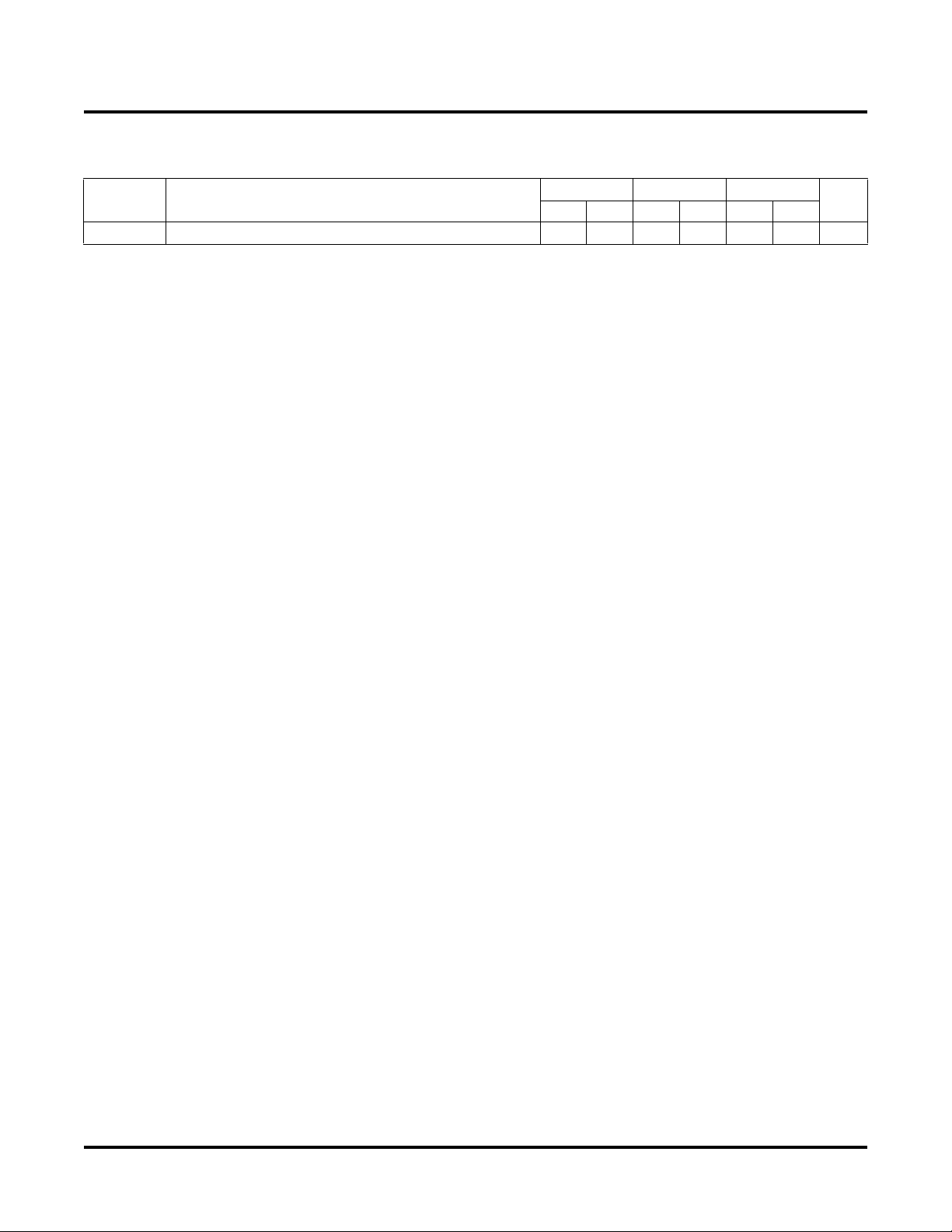
Table 1. ispMACH 4000V/B/C Family Selection Guide
ispMACH
4032V/B/C
Macrocells 32 64 128 256 384 512
I/O + Dedicated Inputs 30+2/32+4 30+2/32+4/
t
(ns) 2.52.52.73.03.53.5
PD
t
(ns) 1.81.81.82.02.02.0
S
t
(ns) 2.22.22.72.72.72.7
CO
f
(MHz) 400 400 333 322 322 322
MAX
Supply Voltages (V) 3.3/2.5/1.8V 3.3/2.5/1.8V 3.3/2.5/1.8V 3.3/2.5/1.8V 3.3/2.5/1.8V 3.3/2.5/1.8V
Pins/Package 44 TQFP
48 TQFP
1. 3.3V (4000V) only.
2. 128-I/O and 160-I/O configurations.
3. Use 256 ftBGA package for all new designs. Refer to PCN#14A-07 for 256 fpBGA package discontinuance.
© 2009 Lattice Semiconductor Corp. All Lattice trademarks, registered trademarks, patents, and disclaimers are as listed at www.latticesemi.com/legal. All other brand
or product names are trademarks or registered trademarks of their respective holders. The specifications and information herein are subject to change without notice.
ispMACH
4064V/B/C
64+10
44 TQFP
48 TQFP
100 TQFP 100 TQFP
ispMACH
4128V/B/C
64+10/92+4/
96+4
128 TQFP
144 TQFP
64+10/96+14/
128+4/160+4
1
ispMACH
4256V/B/C
100 TQFP
144 TQFP
176 TQFP
256 ftBGA
fpBGA
2, 3
ispMACH
4384V/B/C
128+4/192+4 128+4/208+4
1
176 TQFP
2
/
256 ftBGA/
fpBGA
3
ispMACH
4512V/B/C
176 TQFP
256 ftBGA/
fpBGA
3
www.latticesemi.com 1 DS1020_23.1
Page 2

Lattice Semiconductor ispMACH 4000V/B/C/Z Family Data Sheet
Table 2. ispMACH 4000Z Family Selection Guide
ispMACH 4032ZC ispMACH 4064ZC ispMACH 4128ZC ispMACH 4256ZC
Macrocells 32 64 128 256
I/O + Dedicated Inputs 32+4/32+4 32+4/32+12/
tPD (ns) 3.5 3.7 4.2 4.5
t
(ns) 2.2 2.5 2.7 2.9
S
tCO (ns) 3.0 3.2 3.5 3.8
f
(MHz) 267 250 220 200
MAX
Supply Voltage (V) 1.8 1.8 1.8 1.8
Max. Standby Icc (µA) 20 25 35 55
Pins/Package 48 TQFP
56 csBGA
64+10/64+10
48 TQFP
56 csBGA
100 TQFP
132 csBGA
64+10/96+4 64+10/96+6/
100 TQFP
132csBGA
128+4
100 TQFP
132 csBGA
176 TQFP
ispMACH 4000 Introduction
The high performance ispMACH 4000 family from Lattice offers a SuperFAST CPLD solution. The family is a blend
of Lattice’s two most popular architectures: the ispLSI
®
2000 and ispMACH 4A. Retaining the best of both families,
the ispMACH 4000 architecture focuses on significant innovations to combine the highest performance with low
power in a flexible CPLD family.
The ispMACH 4000 combines high speed and low power with the flexibility needed for ease of design. With its
robust Global Routing Pool and Output Routing Pool, this family delivers excellent First-Time-Fit, timing predictability, routing, pin-out retention and density migration.
The ispMACH 4000 family offers densities ranging from 32 to 512 macrocells. There are multiple density-I/O combinations in Thin Quad Flat Pack (TQFP), Chip Scale BGA (csBGA) and Fine Pitch Thin BGA (ftBGA) packages
ranging from 44 to 256 pins/balls. Table 1 shows the macrocell, package and I/O options, along with other key
parameters.
The ispMACH 4000 family has enhanced system integration capabilities. It supports 3.3V (4000V), 2.5V (4000B)
and 1.8V (4000C/Z) supply voltages and 3.3V, 2.5V and 1.8V interface voltages. Additionally, inputs can be safely
driven up to 5.5V when an I/O bank is configured for 3.3V operation, making this family 5V tolerant. The ispMACH
4000 also offers enhanced I/O features such as slew rate control, PCI compatibility, bus-keeper latches, pull-up
resistors, pull-down resistors, open drain outputs and hot socketing. The ispMACH 4000 family members are 3.3V/
2.5V/1.8V in-system programmable through the IEEE Standard 1532 interface. IEEE Standard 1149.1 boundary
scan testing capability also allows product testing on automated test equipment. The 1532 interface signals TCK,
TMS, TDI and TDO are referenced to V
(logic core).
CC
Overview
The ispMACH 4000 devices consist of multiple 36-input, 16-macrocell Generic Logic Blocks (GLBs) interconnected
by a Global Routing Pool (GRP). Output Routing Pools (ORPs) connect the GLBs to the I/O Blocks (IOBs), which
contain multiple I/O cells. This architecture is shown in Figure 1.
2
Page 3

Lattice Semiconductor ispMACH 4000V/B/C/Z Family Data Sheet
Figure 1. Functional Block Diagram
V
I/O
Block
I/O Bank 0
I/O
Block
CCO0
GND
GOE0
GOE1
16
16
VCCGND
Generic
Logic
Block
Generic
Logic
Block
CLK0/I
CLK1/I
CLK2/I
CLK3/I
ORP ORP
ORP ORP
Generic
16
Logic
Block
Generic
16 16
Logic
Block
16
16
36
36
36
Global Routing Pool
36
16
TCK
TMS
TDI
TDO
CCO1
V
I/O
Block
I/O
Block
GND
I/O Bank 1
The I/Os in the ispMACH 4000 are split into two banks. Each bank has a separate I/O power supply. Inputs can
support a variety of standards independent of the chip or bank power supply. Outputs support the standards compatible with the power supply provided to the bank. Support for a variety of standards helps designers implement
designs in mixed voltage environments. In addition, 5V tolerant inputs are specified within an I/O bank that is connected to V
of 3.0V to 3.6V for LVCMOS 3.3, LVTTL and PCI interfaces.
CCO
ispMACH 4000 Architecture
There are a total of two GLBs in the ispMACH 4032, increasing to 32 GLBs in the ispMACH 4512. Each GLB has
36 inputs. All GLB inputs come from the GRP and all outputs from the GLB are brought back into the GRP to be
connected to the inputs of any other GLB on the device. Even if feedback signals return to the same GLB, they still
must go through the GRP. This mechanism ensures that GLBs communicate with each other with consistent and
predictable delays. The outputs from the GLB are also sent to the ORP. The ORP then sends them to the associated I/O cells in the I/O block.
Generic Logic Block
The ispMACH 4000 GLB consists of a programmable AND array, logic allocator, 16 macrocells and a GLB clock
generator. Macrocells are decoupled from the product terms through the logic allocator and the I/O pins are decoupled from macrocells through the ORP. Figure 2 illustrates the GLB.
3
Page 4

Lattice Semiconductor ispMACH 4000V/B/C/Z Family Data Sheet
Logic Allocator
36 Inputs
from GRP
16 Macrocells
To ORP
To GRP
To
Product Term
Output Enable
Sharing
1+OE
16 MC Feedback Signals
Clock
Generator
1+OE
1+OE
1+OE
1+OE
1+OE
1+OE
CLK0
CLK1
CLK2
CLK3
1+OE
AND Array
36 Inputs,
83 Product Terms
Figure 2. Generic Logic Block
AND Array
The programmable AND Array consists of 36 inputs and 83 output product terms. The 36 inputs from the GRP are
used to form 72 lines in the AND Array (true and complement of the inputs). Each line in the array can be connected to any of the 83 output product terms via a wired-AND. Each of the 80 logic product terms feed the logic
allocator with the remaining three control product terms feeding the Shared PT Clock, Shared PT Initialization and
Shared PT OE. The Shared PT Clock and Shared PT Initialization signals can optionally be inverted before being
fed to the macrocells.
Every set of five product terms from the 80 logic product terms forms a product term cluster starting with PT0.
There is one product term cluster for every macrocell in the GLB. Figure 3 is a graphical representation of the AND
Array.
4
Page 5

Lattice Semiconductor ispMACH 4000V/B/C/Z Family Data Sheet
PT0
PT1
Cluster 0
PT2
PT3
PT4
In[0]
In[34]
In[35]
Note:
Indicates programmable fuse.
PT80
PT81
PT82
Shared PT Clock
Shared PT Initialization
Shared PTOE
PT76
PT77
PT78
PT79
PT75
Cluster 15
Figure 3. AND Array
Enhanced Logic Allocator
Within the logic allocator, product terms are allocated to macrocells in product term clusters. Each product term
cluster is associated with a macrocell. The cluster size for the ispMACH 4000 family is 4+1 (total 5) product terms.
The software automatically considers the availability and distribution of product term clusters as it fits the functions
within a GLB. The logic allocator is designed to provide three speed paths: 5-PT fast bypass path, 20-PT Speed
Locking path and an up to 80-PT path. The availability of these three paths lets designers trade timing variability for
increased performance.
The enhanced Logic Allocator of the ispMACH 4000 family consists of the following blocks:
• Product Term Allocator
• Cluster Allocator
• Wide Steering Logic
Figure 4 shows a macrocell slice of the Logic Allocator. There are 16 such slices in the GLB.
Figure 4. Macrocell Slice
n
Cluster
Individual Product
Term Allocator
to
n-1ton-2
to
n+1
5-PT
from
Cluster
Allocator
5
from
n-1
n+2
from
n-4
From
n-4
from
n+1
1-80
PTs
To XOR (MC)
To n+4
SuperWIDE™
Steering Logic
Fast 5-PT
Path
Page 6

Lattice Semiconductor ispMACH 4000V/B/C/Z Family Data Sheet
Product Term Allocator
The product term allocator assigns product terms from a cluster to either logic or control applications as required
by the design being implemented. Product terms that are used as logic are steered into a 5-input OR gate associated with the cluster. Product terms that used for control are steered either to the macrocell or I/O cell associated
with the cluster. Table 3 shows the available functions for each of the five product terms in the cluster. The OR gate
output connects to the associated I/O cell, providing a fast path for narrow combinatorial functions, and to the logic
allocator.
Table 3. Individual PT Steering
Product Term Logic Control
PTn Logic PT Single PT for XOR/OR
PT
n+1 Logic PT Individual Clock (PT Clock)
PT
n+2 Logic PT Individual Initialization or Individual Clock Enable (PT Initialization/CE)
PT
n+3 Logic PT Individual Initialization (PT Initialization)
PT
n+4 Logic PT Individual OE (PTOE)
Cluster Allocator
The cluster allocator allows clusters to be steered to neighboring macrocells, thus allowing the creation of functions
with more product terms. Table 4 shows which clusters can be steered to which macrocells. Used in this manner,
the cluster allocator can be used to form functions of up to 20 product terms. Additionally, the cluster allocator
accepts inputs from the wide steering logic. Using these inputs, functions up to 80 product terms can be created.
Table 4. Available Clusters for Each Macrocell
Macrocell Available Clusters
M0 — C0 C1 C2
M1 C0 C1 C2 C3
M2 C1 C2 C3 C4
M3 C2 C3 C4 C5
M4 C3 C4 C5 C6
M5 C4 C5 C6 C7
M6 C5 C6 C7 C8
M7 C6 C7 C8 C9
M8 C7 C8 C9 C10
M9 C8 C9 C10 C11
M10 C9 C10 C11 C12
M11 C10 C11 C12 C13
M12 C11 C12 C13 C14
M13 C12 C13 C14 C15
M14 C13 C14 C15 —
M15 C14 C15 — —
Wide Steering Logic
The wide steering logic allows the output of the cluster allocator n to be connected to the input of the cluster allocator n+4. Thus, cluster chains can be formed with up to 80 product terms, supporting wide product term functions
and allowing performance to be increased through a single GLB implementation. Table 5 shows the product term
chains.
6
Page 7

Lattice Semiconductor ispMACH 4000V/B/C/Z Family Data Sheet
Table 5. Product Term Expansion Capability
Expansion
Chains
Macrocells Associated with Expansion Chain
(with Wrap Around)
Max PT/
Macrocell
Chain-0 M0 M4 M8 M12 M0 75
Chain-1 M1 M5 M9 M13 M1 80
Chain-2 M2 M6 M10 M14 M2 75
Chain-3 M3 M7 M11 M15 M3 70
Every time the super cluster allocator is used, there is an incremental delay of t
. When the super cluster alloca-
EXP
tor is used, all destinations other than the one being steered to, are given the value of ground (i.e., if the super cluster is steered to M (n+4), then M (n) is ground).
Macrocell
The 16 macrocells in the GLB are driven by the 16 outputs from the logic allocator. Each macrocell contains a programmable XOR gate, a programmable register/latch, along with routing for the logic and control functions.
Figure 5 shows a graphical representation of the macrocell. The macrocells feed the ORP and GRP. A direct input
from the I/O cell allows designers to use the macrocell to construct high-speed input registers. A programmable
delay in this path allows designers to choose between the fastest possible set-up time and zero hold time.
Figure 5. Macrocell
Power-up
Initialization
Shared PT Initialization
PT Initialization (optional)
PT Initialization/CE (optional)
Single PT
From Logic Allocator
Block CLK0
Block CLK1
Block CLK2
Block CLK3
PT Clock (optional)
Shared PT Clock
Delay
RP
D/T/L Q
CE
From I/O Cell
To ORP
To GRP
Enhanced Clock Multiplexer
The clock input to the flip-flop can select any of the four block clocks along with the shared PT clock, and true and
complement forms of the optional individual term clock. An 8:1 multiplexer structure is used to select the clock. The
eight sources for the clock multiplexer are as follows:
• Block CLK0
• Block CLK1
7
Page 8

Lattice Semiconductor ispMACH 4000V/B/C/Z Family Data Sheet
• Block CLK2
• Block CLK3
• PT Clock
• PT Clock Inverted
• Shared PT Clock
•Ground
Clock Enable Multiplexer
Each macrocell has a 4:1 clock enable multiplexer. This allows the clock enable signal to be selected from the following four sources:
• PT Initialization/CE
• PT Initialization/CE Inverted
• Shared PT Clock
• Logic High
Initialization Control
The ispMACH 4000 family architecture accommodates both block-level and macrocell-level set and reset capability.
There is one block-level initialization term that is distributed to all macrocell registers in a GLB. At the macrocell
level, two product terms can be “stolen” from the cluster associated with a macrocell to be used for set/reset functionality. A reset/preset swapping feature in each macrocell allows for reset and preset to be exchanged, providing
flexibility.
Note that the reset/preset swapping selection feature affects power-up reset as well. All flip-flops power up to a
known state for predictable system initialization. If a macrocell is configured to SET on a signal from the block-level
initialization, then that macrocell will be SET during device power-up. If a macrocell is configured to RESET on a
signal from the block-level initialization or is not configured for set/reset, then that macrocell will RESET on powerup. To guarantee initialization values, the V
rise must be monotonic, and the clock must be inactive until the reset
CC
delay time has elapsed.
GLB Clock Generator
Each ispMACH 4000 device has up to four clock pins that are also routed to the GRP to be used as inputs. These
pins drive a clock generator in each GLB, as shown in Figure 6. The clock generator provides four clock signals that
can be used anywhere in the GLB. These four GLB clock signals can consist of a number of combinations of the
true and complement edges of the global clock signals.
Figure 6. GLB Clock Generator
CLK0
Block CLK0
CLK1
CLK2
Block CLK1
Block CLK2
CLK3
Block CLK3
8
Page 9

Lattice Semiconductor ispMACH 4000V/B/C/Z Family Data Sheet
Output Routing Multiplexer
OE Routing Multiplexer
ORP
Bypass
Multiplexer
From Macrocell
From PTOE
To I/O
Cell
To I/O
Cell
Output
OE
5-PT Fast Path
Output Routing Pool (ORP)
The Output Routing Pool allows macrocell outputs to be connected to any of several I/O cells within an I/O block.
This provides greater flexibility in determining the pinout and allows design changes to occur without affecting the
pinout. The output routing pool also provides a parallel capability for routing macrocell-level OE product terms. This
allows the OE product term to follow the macrocell output as it is switched between I/O cells. Additionally, the output routing pool allows the macrocell output or true and complement forms of the 5-PT bypass signal to bypass the
output routing multiplexers and feed the I/O cell directly. The enhanced ORP of the ispMACH 4000 family consists
of the following elements:
• Output Routing Multiplexers
• OE Routing Multiplexers
• Output Routing Pool Bypass Multiplexers
Figure 7 shows the structure of the ORP from the I/O cell perspective. This is referred to as an ORP slice. Each
ORP has as many ORP slices as there are I/O cells in the corresponding I/O block.
Figure 7. ORP Slice
Output Routing Multiplexers
The details of connections between the macrocells and the I/O cells vary across devices and within a device
dependent on the maximum number of I/Os available. Tables 5-9 provide the connection details.
Table 6. ORP Combinations for I/O Blocks with 8 I/Os
I/O Cell Available Macrocells
I/O 0 M0, M1, M2, M3, M4, M5, M6, M7
I/O 1 M2, M3, M4, M5, M6, M7, M8, M9
I/O 2 M4, M5, M6, M7, M8, M9, M10, M11
I/O 3 M6, M7, M8, M9, M10, M11, M12, M13
I/O 4 M8, M9, M10, M11, M12, M13, M14, M15
I/O 5 M10, M11, M12, M13, M14, M15, M0, M1
I/O 6 M12, M13, M14, M15, M0, M1, M2, M3
I/O 7 M14, M15, M0, M1, M2, M3, M4, M5
9
Page 10

Lattice Semiconductor ispMACH 4000V/B/C/Z Family Data Sheet
Table 7. ORP Combinations for I/O Blocks with 16 I/Os
I/O Cell Available Macrocells
I/O 0 M0, M1, M2, M3, M4, M5, M6, M7
I/O 1 M1, M2, M3, M4, M5, M6, M7, M8
I/O 2 M2, M3, M4, M5, M6, M7, M8, M9
I/O 3 M3, M4, M5, M6, M7, M8, M9, M10
I/O 4 M4, M5, M6, M7, M8, M9, M10, M11
I/O 5 M5, M6, M7, M8, M9, M10, M11, M12
I/O 6 M6, M7, M8, M9, M10, M11, M12, M13
I/O 7 M7, M8, M9, M10, M11, M12, M13, M14
I/O 8 M8, M9, M10, M11, M12, M13, M14, M15
I/O 9 M9, M10, M11, M12, M13, M14, M15, M0
I/O 10 M10, M11, M12, M13, M14, M15, M0, M1
I/O 11 M11, M12, M13, M14, M15, M0, M1, M2
I/O 12 M12, M13, M14, M15, M0, M1, M2, M3
I/O 13 M13, M14, M15, M0, M1, M2, M3, M4
I/O 14 M14, M15, M0, M1, M2, M3, M4, M5
I/O 15 M15, M0, M1, M2, M3, M4, M5, M6
Table 8. ORP Combinations for I/O Blocks with 4 I/Os
I/O Cell Available Macrocells
I/O 0 M0, M1, M2, M3, M4, M5, M6, M7
I/O 1 M4, M5, M6, M7, M8, M9, M10, M11
I/O 2 M8, M9, M10, M11, M12, M13, M14, M15
I/O 3 M12, M13, M14, M15, M0, M1, M2, M3
Table 9. ORP Combinations for I/O Blocks with 10 I/Os
I/O Cell Available Macrocells
I/O 0 M0, M1, M2, M3, M4, M5, M6, M7
I/O 1 M2, M3, M4, M5, M6, M7, M8, M9
I/O 2 M4, M5, M6, M7, M8, M9, M10, M11
I/O 3 M6, M7, M8, M9, M10, M11, M12, M13
I/O 4 M8, M9, M10, M11, M12, M13, M14, M15
I/O 5 M10, M11, M12, M13, M14, M15, M0, M1
I/O 6 M12, M13, M14, M15, M0, M1, M2, M3
I/O 7 M14, M15, M0, M1, M2, M3, M4, M5
I/O 8 M2, M3, M4, M5, M6, M7, M8, M9
I/O 9 M10, M11, M12, M13, M14, M15, M0, M1
10
Page 11

Lattice Semiconductor ispMACH 4000V/B/C/Z Family Data Sheet
GOE 0
From ORP
*Global fuses
From ORP
To Macrocell
To GRP
GOE 1
GOE 2
GOE 3
VCC
V
CCO
V
CCO
**
*
Table 10. ORP Combinations for I/O Blocks with 12 I/Os
I/O Cell Available Macrocells
I/O 0 M0, M1, M2, M3, M4, M5, M6, M7
I/O 1 M1, M2, M3, M4, M5, M6, M7, M8
I/O 2 M2, M3, M4, M5, M6, M7, M8, M9
I/O 3 M4, M5, M6, M7, M8, M9, M10, M11
I/O 4 M5, M6, M7, M8, M9, M10, M11, M12
I/O 5 M6, M7, M8, M9, M10, M11, M12, M13
I/O 6 M8, M9, M10, M11, M12, M13, M14, M15
I/O 7 M9, M10, M11, M12, M13, M14, M15, M0
I/O 8 M10, M11, M12, M13, M14, M15, M0, M1
I/O 9 M12, M13, M14, M15, M0, M1, M2, M3
I/O 10 M13, M14, M15, M0, M1, M2, M3, M4
I/O 11 M14, M15, M0, M1, M2, M3, M4, M5
ORP Bypass and Fast Output Multiplexers
The ORP bypass and fast-path output multiplexer is a 4:1 multiplexer and allows the 5-PT fast path to bypass the
ORP and be connected directly to the pin with either the regular output or the inverted output. This multiplexer also
allows the register output to bypass the ORP to achieve faster t
CO
.
Output Enable Routing Multiplexers
The OE Routing Pool provides the corresponding local output enable (OE) product term to the I/O cell.
I/O Cell
The I/O cell contains the following programmable elements: output buffer, input buffer, OE multiplexer and bus
maintenance circuitry. Figure 8 details the I/O cell.
Figure 8. I/O Cell
Each output supports a variety of output standards dependent on the V
also be configured for open drain operation. Each input can be programmed to support a variety of standards, independent of the V
supplied to its I/O bank. The I/O standards supported are:
CCO
supplied to its I/O bank. Outputs can
CCO
11
Page 12

Lattice Semiconductor ispMACH 4000V/B/C/Z Family Data Sheet
Shared PTOE
(Block 0)
Shared PTOE
(Block n)
Global
Fuses
GOE (0:3)
to I/O cells
Internal Global OE
PT Bus
(4 lines)
4-Bit
Global OE Bus
Global OE
Fuse connection
Hard wired
• LVTTL • LVCMOS 1.8
• LVCMOS 3.3 • 3.3V PCI Compatible
• LVCMOS 2.5
All of the I/Os and dedicated inputs have the capability to provide a bus-keeper latch, Pull-up Resistor or Pull-down
Resistor. A fourth option is to provide none of these. The selection is done on a global basis. The default in both
hardware and software is such that when the device is erased or if the user does not specify, the input structure is
configured to be a Pull-up Resistor.
Each ispMACH 4000 device I/O has an individually programmable output slew rate control bit. Each output can be
individually configured for fast slew or slow slew. The typical edge rate difference between fast and slow slew setting is 20%. For high-speed designs with long, unterminated traces, the slow-slew rate will introduce fewer reflections, less noise and keep ground bounce to a minimum. For designs with short traces or well terminated lines, the
fast slew rate can be used to achieve the highest speed.
Global OE Generation
Most ispMACH 4000 family devices have a 4-bit wide Global OE Bus, except the ispMACH 4032 device that has a
2-bit wide Global OE Bus. This bus is derived from a 4-bit internal global OE PT bus and two dual purpose I/O or
GOE pins. Each signal that drives the bus can optionally be inverted.
Each GLB has a block-level OE PT that connects to all bits of the Global OE PT bus with four fuses. Hence, for a
256-macrocell device (with 16 blocks), each line of the bus is driven from 16 OE product terms. Figures 9 and 10
show a graphical representation of the global OE generation.
Figure 9. Global OE Generation for All Devices Except ispMACH 4032
12
Page 13

Lattice Semiconductor ispMACH 4000V/B/C/Z Family Data Sheet
Shared PTOE
(Block 0)
Shared PTOE
(Block 1)
Global
Fuses
GOE (3:0)
to I/O cells
Internal Global OE
PT Bus
(2 lines)
4-Bit
Global OE Bus
Global OE
Fuse connection
Hard wired
Figure 10. Global OE Generation for ispMACH 4032
Zero Power/Low Power and Power Management
The ispMACH 4000 family is designed with high speed low power design techniques to offer both high speed and
low power. With an advanced E
approach), the ispMACH 4000 family offers SuperFAST pin-to-pin speeds, while simultaneously delivering low
standby power without needing any “turbo bits” or other power management schemes associated with a traditional
sense-amplifier approach.
The zero power ispMACH 4000Z is based on the 1.8V ispMACH 4000C family. With innovative circuit design
changes, the ispMACH 4000Z family is able to achieve the industry’s “lowest static power”.
2
low power cell and non sense-amplifier design approach (full CMOS logic
IEEE 1149.1-Compliant Boundary Scan Testability
All ispMACH 4000 devices have boundary scan cells and are compliant to the IEEE 1149.1 standard. This allows
functional testing of the circuit board on which the device is mounted through a serial scan path that can access all
critical logic notes. Internal registers are linked internally, allowing test data to be shifted in and loaded directly onto
test nodes, or test node data to be captured and shifted out for verification. In addition, these devices can be linked
into a board-level serial scan path for more board-level testing. The test access port operates with an LVCMOS
interface that corresponds to the power supply voltage.
I/O Quick Configuration
To facilitate the most efficient board test, the physical nature of the I/O cells must be set before running any continuity tests. As these tests are fast, by nature, the overhead and time that is required for configuration of the I/Os’
physical nature should be minimal so that board test time is minimized. The ispMACH 4000 family of devices allows
this by offering the user the ability to quickly configure the physical nature of the I/O cells. This quick configuration
takes milliseconds to complete, whereas it takes seconds for the entire device to be programmed. Lattice's ispVM
System programming software can either perform the quick configuration through the PC parallel port, or can generate the ATE or test vectors necessary for a third-party test system.
®
13
Page 14

Lattice Semiconductor ispMACH 4000V/B/C/Z Family Data Sheet
IEEE 1532-Compliant In-System Programming
Programming devices in-system provides a number of significant benefits including: rapid prototyping, lower inventory levels, higher quality and the ability to make in-field modifications. All ispMACH 4000 devices provide In-System Programming (ISP™) capability through the Boundary Scan Test Access Port. This capability has been
implemented in a manner that ensures that the port remains complaint to the IEEE 1149.1 standard. By using IEEE
1149.1 as the communication interface through which ISP is achieved, users get the benefit of a standard, welldefined interface. All ispMACH 4000 devices are also compliant with the IEEE 1532 standard.
The ispMACH 4000 devices can be programmed across the commercial temperature and voltage range. The PCbased Lattice software facilitates in-system programming of ispMACH 4000 devices. The software takes the
JEDEC file output produced by the design implementation software, along with information about the scan chain,
and creates a set of vectors used to drive the scan chain. The software can use these vectors to drive a scan chain
via the parallel port of a PC. Alternatively, the software can output files in formats understood by common automated test equipment. This equipment can then be used to program ispMACH 4000 devices during the testing of a
circuit board.
User Electronic Signature
The User Electronic Signature (UES) allows the designer to include identification bits or serial numbers inside the
device, stored in E
user to store unique data such as ID codes, revision numbers or inventory control codes.
2
CMOS memory. The ispMACH 4000 device contains 32 UES bits that can be configured by the
Security Bit
A programmable security bit is provided on the ispMACH 4000 devices as a deterrent to unauthorized copying of
the array configuration patterns. Once programmed, this bit defeats readback of the programmed pattern by a
device programmer, securing proprietary designs from competitors. Programming and verification are also
defeated by the security bit. The bit can only be reset by erasing the entire device.
Hot Socketing
The ispMACH 4000 devices are well-suited for applications that require hot socketing capability. Hot socketing a
device requires that the device, during power-up and down, can tolerate active signals on the I/Os and inputs without being damaged. Additionally, it requires that the effects of I/O pin loading be minimal on active signals. The ispMACH 4000 devices provide this capability for input voltages in the range 0V to 3.0V.
Density Migration
The ispMACH 4000 family has been designed to ensure that different density devices in the same package have
the same pin-out. Furthermore, the architecture ensures a high success rate when performing design migration
from lower density parts to higher density parts. In many cases, it is possible to shift a lower utilization design targeted for a high density device to a lower density device. However, the exact details of the final resource utilization
will impact the likely success in each case.
14
Page 15

Lattice Semiconductor ispMACH 4000V/B/C/Z Family Data Sheet
Absolute Maximum Ratings
1, 2, 3
ispMACH 4000C/Z ispMACH 4000B ispMACH 4000V
(1.8V) (2.5V) (3.3V)
Supply Voltage (V
Output Supply Voltage (V
Input or I/O Tristate Voltage Applied
) . . . . . . . . . . . . . . . . . . . . . . -0.5 to 2.5V . . . . . . . . . .-0.5 to 5.5V. . . . . . . . . . . -0.5 to 5.5V
CC
) . . . . . . . . . . . . . . . -0.5 to 4.5V . . . . . . . . . .-0.5 to 4.5V. . . . . . . . . . . -0.5 to 4.5V
CCO
4, 5
. . . . . . . . . -0.5 to 5.5V . . . . . . . . . .-0.5 to 5.5V. . . . . . . . . . . -0.5 to 5.5V
Storage Temperature . . . . . . . . . . . . . . . . . . . . . . -65 to 150C. . . . . . . . . -65 to 150C . . . . . . . . . .-65 to 150C
Junction Temperature (T
1. Stress above those listed under the “Absolute Maximum Ratings” may cause permanent damage to the device. Functional
operation of the device at these or any other conditions above those indicated in the operational sections of this specification
is not implied.
2. Compliance with Lattice Thermal Management
3. All voltages referenced to GND.
4. Undershoot of -2V and overshoot of (V
5. Maximum of 64 I/Os per device with VIN > 3.6V is allowed.
) with Power Applied . . .-55 to 150C . . . . . . . . . -55 to 150C . . . . . . . . . .-55 to 150C
j
document is required.
(MAX) + 2V), up to a total pin voltage of 6.0V, is permitted for a duration of < 20ns.
IH
Recommended Operating Conditions
Symbol Parameter Min. Max. Units
ispMACH 4000C 1.65 1.95 V
Supply Voltage for 1.8V Devices
V
CC
Supply Voltage for 2.5V Devices 2.3 2.7 V
Supply Voltage for 3.3V Devices 3.0 3.6 V
Junction Temperature (Commercial) 0 90 C
T
j
Junction Temperature (Industrial) -40 105 C
Junction Temperature (Extended) -40 130 C
1. Devices operating at 1.6V can expect performance degradation up to 35%.
2. Applicable for devices with 2004 date codes and later. Contact factory for ordering instructions.
ispMACH 4000Z 1.7 1.9 V
ispMACH 4000Z, Extended Functional Voltage
Operation
1.6
1, 2
1.9 V
Erase Reprogram Specifications
Parameter Min. Max. Units
Erase/Reprogram Cycle 1,000 — Cycles
Note: Valid over commercial temperature range.
Hot Socketing Characteristics
Symbol Parameter Condition Min. Typ. Max. Units
I
DK
1. Insensitive to sequence of VCC or V
2. 0 < V
3. I
DK
Input or I/O Leakage Current
However, assumes monotonic rise/fall rates for VCC and V
< VCC (MAX), 0 < V
CC
is additive to IPU, IPD or IBH. Device defaults to pull-up until fuse circuitry is active.
CCO
< V
CCO.
CCO
(MAX).
1,2,3
3.0V, Tj = 105°C — ±30 ±150 µA
0 V
IN
0 VIN 3.0V, Tj = 130°C — ±30 ±200 µA
provided (VIN - V
CCO,
CCO
) 3.6V.
15
Page 16

Lattice Semiconductor ispMACH 4000V/B/C/Z Family Data Sheet
I/O Recommended Operating Conditions
1
(V)
V
CCO
Standard
Min. Max.
LV TT L 3 .0 3 .6
LVCMOS 3.3 3.0 3.6
Extended LVCMOS 3.3
2
2.7 3.6
LVCMOS 2.5 2.3 2.7
LVCMOS 1.8 1.65 1.95
PCI 3.3 3.0 3.6
1. Typical values for V
2. ispMACH 4000Z only.
are the average of the min. and max. values.
CCO
DC Electrical Characteristics
Over Recommended Operating Conditions
Symbol Parameter Condition Min. Typ. Max. Units
Input Leakage Current (ispMACH
1, 4
I
, I
IL
IH
4000Z)
1
I
IH
, I
I
IL
1,2
I
IH
Input High Leakage Current (ispMACH 4000Z)
Input Leakage Current (ispMACH
1
IH
4000V/B/C)
Input High Leakage Current (ispMACH 4000V/B/C)
I/O Weak Pull-up Resistor Current
I
PU
(ispMACH 4000Z)
I/O Weak Pull-up Resistor Current
(ispMACH 4000V/B/C)
I
PD
I
BHLS
I
BHHS
I
BHLO
I
BHHO
V
BHT
C
1
C
2
C
3
1. Input or I/O leakage current is measured with the pin configured as an input or as an I/O with the output driver tristated. It is not
2. 5V tolerant inputs and I/O should only be placed in banks where 3.0V
3. T
4. I
I/O Weak Pull-down Resistor Current VIL (MAX) VIN VIH (MIN) 30 — 150 µA
Bus Hold Low Sustaining Current VIN = VIL (MAX) 30 — — µA
Bus Hold High Sustaining Current VIN = 0.7 V
Bus Hold Low Overdrive Current 0V VIN V
Bus Hold High Overdrive Current V
Bus Hold Trip Points — V
I/O Capacitance
Clock Capacitance
Global Input Capacitance
measured with the output driver active. Bus maintenance circuits are disabled.
= 25°C, f = 1.0MHz
A
excursions of up to 1.5µA maximum per pin above the spec limit may be observed for certain voltage conditions on no more than 10% of
IH
the device’s I/O pins.
3
3
3
< V
0 V
IN
CCO
< VIN 5.5V — — 10 µA
V
CCO
—0.51µA
0 VIN 3.6V, Tj = 105°C — — 10 µA
0 V
3.6V, Tj = 130°C — — 15 µA
IN
3.6V < V
3.0V V
3.6V < V
3.0V V
0 VIN 0.7V
0 V
BHT
V
CCO
VCC = 1.8V, VIO = 0 to VIH (MAX) — —
V
CCO
V
CC
V
CCO
V
CC
5.5V, Tj = 105°C
IN
3.6V
CCO
5.5V, Tj = 130°C
IN
3.6V
CCO
CCO
0.7V
IN
VIN V
CCO
CCO
BHT
CCO
= 3.3V, 2.5V, 1.8V —
= 3.3V, 2.5V, 1.8V —
= 1.8V, VIO = 0 to VIH (MAX) — —
= 3.3V, 2.5V, 1.8V —
= 1.8V, VIO = 0 to VIH (MAX) — —
V
3.6V.
CCO
——20µA
——50µA
-30 — -150 µA
-30 — -200 µA
-30 — — µA
— — 150 µA
——-150µA
* 0.35 — V
CCO
CCO
8
6
6
—
—
—
* 0.65 V
pf
pf
pf
16
Page 17

Lattice Semiconductor ispMACH 4000V/B/C/Z Family Data Sheet
Supply Current, ispMACH 4000V/B/C
Over Recommended Operating Conditions
Symbol Parameter Condition Min. Typ. Max. Units
ispMACH 4032V/B/C
Vcc = 3.3V — 11.8 — mA
1,2,3
ICC
4
ICC
ispMACH 4064V/B/C
1,2,3
ICC
5
ICC
ispMACH 4128V/B/C
1,2,3
ICC
4
ICC
ispMACH 4256V/B/C
1,2,3
I
CC
4
I
CC
ispMACH 4384V/B/C
1,2,3
I
CC
4
I
CC
ispMACH 4512V/B/C
1,2,3
I
CC
Operating Power Supply Current
Standby Power Supply Current
Operating Power Supply Current
Standby Power Supply Current
Operating Power Supply Current
Standby Power Supply Current
Operating Power Supply Current
Standby Power Supply Current
Operating Power Supply Current
Standby Power Supply Current
Operating Power Supply Current
Vcc = 2.5V — 11.8 — mA
Vcc = 1.8V — 1.8 — mA
Vcc = 3.3V — 11.3 — mA
Vcc = 2.5V — 11.3 — mA
Vcc = 1.8V — 1.3 — mA
Vcc = 3.3V — 12 — mA
Vcc = 2.5V — 12 — mA
Vcc = 1.8V — 2 — mA
Vcc = 3.3V — 11.5 — mA
Vcc = 2.5V — 11.5 — mA
Vcc = 1.8V — 1.5 — mA
Vcc = 3.3V — 12 — mA
Vcc = 2.5V — 12 — mA
Vcc = 1.8V — 2 — mA
Vcc = 3.3V — 11.5 — mA
Vcc = 2.5V — 11.5 — mA
Vcc = 1.8V — 1.5 — mA
Vcc = 3.3V — 12.5 — mA
Vcc = 2.5V — 12.5 — mA
Vcc = 1.8V — 2.5 — mA
Vcc = 3.3V — 12 — mA
Vcc = 2.5V — 12 — mA
Vcc = 1.8V — 2 — mA
Vcc = 3.3V — 13.5 — mA
Vcc = 2.5V — 13.5 — mA
Vcc = 1.8V — 3.5 — mA
Vcc = 3.3V — 12.5 — mA
Vcc = 2.5V — 12.5 — mA
Vcc = 1.8V — 2.5 — mA
Vcc = 3.3V — 14 — mA
Vcc = 2.5V — 14 — mA
Vcc = 1.8V — 4 — mA
17
Page 18

Lattice Semiconductor ispMACH 4000V/B/C/Z Family Data Sheet
Supply Current, ispMACH 4000V/B/C (Cont.)
Over Recommended Operating Conditions
Symbol Parameter Condition Min. Typ. Max. Units
Vcc = 3.3V — 13 — mA
4
I
CC
1. TA = 25°C, frequency = 1.0 MHz.
2. Device configured with 16-bit counters.
3. I
varies with specific device configuration and operating frequency.
CC
4. T
= 25°C
A
Standby Power Supply Current
Vcc = 2.5V — 13 — mA
Vcc = 1.8V — 3 — mA
Supply Current, ispMACH 4000Z
Over Recommended Operating Conditions
Symbol Parameter Condition Min. Typ. Max. Units
ispMACH 4032ZC
= 25°C — 50 — µA
A
= 70°C — 58 — µA
A
= 125°C — 70 — µA
A
= 25°C — 10 — µA
A
= 85°C — 15 25 µA
A
= 125°C — 22 — µA
A
= 25°C — 80 — µA
A
= 70°C — 89 — µA
A
= 125°C — 109 — µA
A
= 25°C — 11 — µA
A
= 85°C — 18 35 µA
A
= 125°C — 37 — µA
A
= 25°C — 168 — µA
A
= 70°C — 190 — µA
A
= 125°C — 212 — µA
A
= 25°C — 12 — µA
A
= 85°C — 19 50 µA
A
= 125°C — 42 — µA
A
ICC
ICC
1, 2, 3, 5
4, 5
Operating Power Supply Current
Standby Power Supply Current
ispMACH 4064ZC
ICC
ICC
1, 2, 3, 5
4, 5
Operating Power Supply Current
Standby Power Supply Current
ispMACH 4128ZC
ICC
ICC
1, 2, 3, 5
4, 5
Operating Power Supply Current
Standby Power Supply Current
Vcc = 1.8V, T
Vcc = 1.9V, T
Vcc = 1.9V, TA = 85°C — 60 — µA
Vcc = 1.9V, T
Vcc = 1.8V, T
Vcc = 1.9V, TA = 70°C — 13 20 µA
Vcc = 1.9V, T
Vcc = 1.9V, T
Vcc = 1.8V, T
Vcc = 1.9V, T
Vcc = 1.9V, TA = 85°C — 92 — µA
Vcc = 1.9V, T
Vcc = 1.8V, T
Vcc = 1.9V, TA = 70°C — 15 25 µA
Vcc = 1.9V, T
Vcc = 1.9V, T
Vcc = 1.8V, T
Vcc = 1.9V, T
Vcc = 1.9V, TA = 85°C — 195 — µA
Vcc = 1.9V, T
Vcc = 1.8V, T
Vcc = 1.9V, TA = 70°C — 16 35 µA
Vcc = 1.9V, T
Vcc = 1.9V, T
18
Page 19

Lattice Semiconductor ispMACH 4000V/B/C/Z Family Data Sheet
Supply Current, ispMACH 4000Z (Cont.)
Over Recommended Operating Conditions
Symbol Parameter Condition Min. Typ. Max. Units
ispMACH 4256ZC
= 25°C — 341 — µA
A
= 70°C — 361 — µA
A
= 125°C — 468 — µA
A
= 25°C — 13 — µA
A
= 85°C — 43 90 µA
A
= 125°C — 135 — µA
A
1, 2, 3, 5
ICC
4, 5
ICC
1. TA = 25°C, frequency = 1.0 MHz.
2. Device configured with 16-bit counters.
3. I
CC
4. V
CCO
5. Includes V
Operating Power Supply Current
Standby Power Supply Current
varies with specific device configuration and operating frequency.
= 3.6V, VIN = 0V or V
current without output loading.
CCO
bus maintenance turned off. VIN above V
CCO,
Vcc = 1.8V, T
Vcc = 1.9V, T
Vcc = 1.9V, TA = 85°C — 372 — µA
Vcc = 1.9V, T
Vcc = 1.8V, T
Vcc = 1.9V, TA = 70°C — 32 55 µA
Vcc = 1.9V, T
Vcc = 1.9V, T
will add transient current above the specified standby ICC.
CCO
19
Page 20

Lattice Semiconductor ispMACH 4000V/B/C/Z Family Data Sheet
I/O DC Electrical Characteristics
Over Recommended Operating Conditions
V
IL
Standard
LVTTL -0.3 0.80 2.0 5.5
LVCMOS 3.3 -0.3 0.80 2.0 5.5
LVCMOS 2.5 -0.3 0.70 1.70 3.6
LVC M OS 1. 8
(4000V/B)
LVC M OS 1. 8
(4000C/Z)
-0.3 0.63 1.17 3.6
-0.3 0.35 * V
CC
0.65 * V
PCI 3.3 (4000V/B) -0.3 1.08 1.5 5.5 0.1 V
PCI 3.3 (4000C/Z) -0.3 0.3 * 3.3 * (V
1. The average DC current drawn by I/Os between adjacent bank GND connections, or between the last GND in an I/O bank and the end of
the I/O bank, as shown in the logic signals connection table, shall not exceed n*8mA. Where n is the number of I/Os between bank GND
connections or between the last GND in a bank and the end of a bank.
1.8) 0.5 * 3.3 * (V
CC /
V
IH
CC
1.8) 5.5 0.1 V
CC /
3.6
V
OL
Max (V)
0.40 V
0.20 V
0.40 V
0.20 V
0.40 V
0.20 V
0.40 V
0.20 V
0.40 V
0.20 V
CCO
CCO
V
OH
Min (V)
- 0.40 8.0 -4.0
CCO
- 0.20 0.1 -0.1
CCO
- 0.40 8.0 -4.0
CCO
- 0.20 0.1 -0.1
CCO
- 0.40 8.0 -4.0
CCO
- 0.20 0.1 -0.1
CCO
- 0.45 2.0 -2.0
CCO
- 0.20 0.1 -0.1
CCO
- 0.45 2.0 -2.0
CCO
- 0.20 0.1 -0.1
CCO
0.9 V
CCO
0.9 V
CCO
I
(mA)
1.5 -0.5
1.5 -0.5
OL
1
1
I
OH
(mA)Min (V) Max (V) Min (V) Max (V)
20
Page 21

Lattice Semiconductor ispMACH 4000V/B/C/Z Family Data Sheet
VO Output Voltage (V)
Typical I/O Output Current (mA)
3.3V V
CCO
VO Output Voltage (V)
0
0
0
20
40
60
80
100
10
20
30
40
50
60
0
10
20
30
40
50
60
70
2.01.51.00.5
0 2.0 2.5 3.0 3.51.51.00.5
0 2.0 2.51.51.00.5
Typical I/O Output Current (mA)
1.8V V
CCO
VO Output Voltage (V)
I
OH
Typical I/O Output Current (mA)
2.5V V
CCO
I
OL
I
OH
I
OL
I
OH
I
OL
21
Page 22

Lattice Semiconductor ispMACH 4000V/B/C/Z Family Data Sheet
ispMACH 4000V/B/C External Switching Characteristics
Over Recommended Operating Conditions
-25 -27 -3 -35
Parameter Description
t
PD
t
PD_MC
t
S
t
ST
t
SIR
t
SIRZ
t
H
t
HT
t
HIR
t
HIRZ
t
CO
t
R
t
RW
t
PTOE/DIS
t
GPTOE/DIS
t
GOE/DIS
t
CW
t
GW
t
WIR
4
f
MAX
f
(Ext.)
MAX
1. Timing numbers are based on default LVCMOS 1.8 I/O buffers. Use timing adjusters provided to calculate other standards. Timing v.3.2
2. Measured using standard switching circuit, assuming GRP loading of 1 and 1 output switching.
3. Pulse widths and clock widths less than minimum will cause unknown behavior.
4. Standard 16-bit counter using GRP feedback.
5-PT bypass combinatorial propagation
delay
20-PT combinatorial propagation delay
through macrocell
GLB register setup time before clock 1.8 — 1.8 — 2.0 — 2.0 — ns
GLB register setup time before clock
with T-type register
GLB register setup time before clock,
input register path
GLB register setup time before clock
with zero hold
GLB register hold time after clock 0.0 — 0.0 — 0.0 — 0.0 — ns
GLB register hold time after clock with
T-type register
GLB register hold time after clock, input
register path
GLB register hold time after clock, input
register path with zero hold
GLB register clock-to-output delay — 2.2 — 2.7 — 2.7 — 2.7 ns
External reset pin to output delay — 3.5 — 4.0 — 4.4 — 4.5 ns
External reset pulse duration 1.5 — 1.5 — 1.5 — 1.5 - ns
Input to output local product term output
enable/disable
Input to output global product term
output enable/disable
Global OE input to output enable/disable — 3.0 — 3.5 — 4.0 — 4.5 ns
Global clock width, high or low 1.1 — 1.3 — 1.3 — 1.3 — ns
Global gate width low (for low
transparent) or high (for high transparent)
Input register clock width, high or low 1.1 — 1.3 — 1.3 — 1.3 — ns
Clock frequency with internal feedback — 400 — 333 — 322 — 322 MHz
Clock frequency with external feedback,
+ tCO)]
[1/ (t
S
1, 2, 3
—2.5—2.7—3.0—3.5ns
—3.2—3.5—3.8—4.2ns
2.0 — 2.0 — 2.2 — 2.2 — ns
0.7 — 1.0 — 1.0 — 1.0 — ns
1.7 — 2.0 — 2.0 — 2.0 — ns
0.0 — 0.0 — 0.0 — 0.0 — ns
0.9 — 1.0 — 1.0 — 1.0 — ns
0.0 — 0.0 — 0.0 — 0.0 — ns
—4.0—4.5—5.0—5.5ns
—5.0—6.5—8.0—8.0ns
1.1 — 1.3 — 1.3 — 1.3 — ns
— 250 — 222 — 212 — 212 MHz
UnitsMin. Max. Min. Max. Min. Max. Min. Max.
22
Page 23

Lattice Semiconductor ispMACH 4000V/B/C/Z Family Data Sheet
ispMACH 4000V/B/C External Switching Characteristics (Cont.)
Over Recommended Operating Conditions
-5 -75 -10
Parameter Description
t
PD
t
PD_MC
t
S
t
ST
t
SIR
t
SIRZ
t
H
t
HT
t
HIR
t
HIRZ
t
CO
t
R
t
RW
t
PTOE/DIS
t
GPTOE/DIS
t
GOE/DIS
t
CW
t
GW
t
WIR
4
f
MAX
f
(Ext.) Clock frequency with external feedback, [1/ (tS + tCO)] —156—111— 86MHz
MAX
1. Timing numbers are based on default LVCMOS 1.8 I/O buffers. Use timing adjusters provided to calculate other standards. Timing v.3.2
2. Measured using standard switching circuit, assuming GRP loading of 1 and 1 output switching.
3. Pulse widths and clock widths less than minimum will cause unknown behavior.
4. Standard 16-bit counter using GRP feedback.
5-PT bypass combinatorial propagation delay — 5.0 — 7.5 — 10.0 ns
20-PT combinatorial propagation delay through macrocell — 5.5 — 8.0 — 10.5 ns
GLB register setup time before clock 3.0 — 4.5 — 5.5 — ns
GLB register setup time before clock with T-type register 3.2 — 4.7 — 5.5 — ns
GLB register setup time before clock, input register path 1.2 — 1.7 — 1.7 — ns
GLB register setup time before clock with zero hold 2.2 — 2.7 — 2.7 — ns
GLB register hold time after clock 0.0 — 0.0 — 0.0 — ns
GLB register hold time after clock with T-type register 0.0 — 0.0 — 0.0 — ns
GLB register hold time after clock, input register path 1.0 — 1.0 — 1.0 — ns
GLB register hold time after clock, input register path with
zero hold
GLB register clock-to-output delay — 3.4 — 4.5 — 6.0 ns
External reset pin to output delay — 6.3 — 9.0 — 10.5 ns
External reset pulse duration 2.0 — 4.0 — 4.0 — ns
Input to output local product term output enable/disable — 7.0 — 9.0 — 10.5 ns
Input to output global product term output enable/disable — 9.0 — 10.3 — 12.0 ns
Global OE input to output enable/disable — 5.0 — 7.0 — 8.0 ns
Global clock width, high or low 2.2 — 2.8 — 4.0 — ns
Global gate width low (for low transparent) or high (for
high transparent)
Input register clock width, high or low 2.2 — 2.8 — 4.0 ns
Clock frequency with internal feedback — 227 — 168 — 125 MHz
1, 2, 3
0.0 — 0.0 — 0.0 — ns
2.2 — 2.8 — 4.0 — ns
UnitsMin. Max. Min. Max. Min. Max.
23
Page 24

Lattice Semiconductor ispMACH 4000V/B/C/Z Family Data Sheet
ispMACH 4000Z External Switching Characteristics
Over Recommended Operating Conditions
-35 -37 -42
Parameter Description
t
PD
t
PD_MC
t
S
t
ST
t
SIR
t
SIRZ
t
H
t
HT
t
HIR
t
HIRZ
t
CO
t
R
t
RW
t
PTOE/DIS
t
GPTOE/DIS
t
GOE/DIS
t
CW
t
GW
t
WIR
4
f
MAX
(Ext.)
f
MAX
1. Timing numbers are based on default LVCMOS 1.8 I/O buffers. Use timing adjusters provided to calculate other standards. Timing v.2.2
2. Measured using standard switching GRP loading of 1 and 1 output switching.
3. Pulse widths and clock widths less than minimum will cause unknown behavior.
4. Standard 16-bit counter using GRP feedback.
5-PT bypass combinatorial propagation delay — 3.5 — 3.7 — 4.2 ns
20-PT combinatorial propagation delay
through macrocell
GLB register setup time before clock 2.2 — 2.5 — 2.7 — ns
GLB register setup time before clock with
T-type register
GLB register setup time before clock, input
register path
GLB register setup time before clock with zero
hold
GLB register hold time after clock 0.0 — 0.0 — 0.0 — ns
GLB register hold time after clock with T-type
register
GLB register hold time after clock, input
register path
GLB register hold time after clock, input
register path with zero hold
GLB register clock-to-output delay — 3.0 — 3.2 — 3.5 ns
External reset pin to output delay — 5.0 — 6.0 — 7.3 ns
External reset pulse duration 1.5 — 1.7 — 2.0 — ns
Input to output local product term output
enable/disable
Input to output global product term output
enable/disable
Global OE input to output enable/disable — 4.5 — 4.5 — 4.8 ns
Global clock width, high or low 1.0 — 1.5 — 1.8 — ns
Global gate width low (for low transparent) or
high (for high transparent)
Input register clock width, high or low 1.0 — 1.5 — 1.8 — ns
Clock frequency with internal feedback — 267 — 250 — 220 MHz
clock frequency with external feedback,
[1 / (tS + tCO)]
1, 2, 3
—4.4—4.7—5.7 ns
2.4 — 2.7 — 2.9 — ns
1.0 — 1.1 — 1.3 — ns
2.0 — 2.1 — 2.6 — ns
0.0 — 0.0 — 0.0 — ns
1.0 — 1.0 — 1.3 — ns
0.0 — 0.0 — 0.0 — ns
—7.0—8.0—8.0 ns
—6.5—7.0—8.0 ns
1.0 — 1.5 — 1.8 — ns
—192—175—161MHz
UnitsMin. Max. Min. Max. Min. Max.
24
Page 25

Lattice Semiconductor ispMACH 4000V/B/C/Z Family Data Sheet
ispMACH 4000Z External Switching Characteristics (Cont.)
Over Recommended Operating Conditions
-45 -5 -75
Parameter Description
t
PD
t
PD_MC
t
S
t
ST
t
SIR
t
SIRZ
t
H
t
HT
t
HIR
t
HIRZ
t
CO
t
R
t
RW
t
PTOE/DIS
t
GPTOE/DIS
t
GOE/DIS
t
CW
t
GW
t
WIR
4
f
MAX
(Ext.)
f
MAX
1. Timing numbers are based on default LVCMOS 1.8 I/O buffers. Use timing adjusters provided to calculate other standards. Timing v.2.2
2. Measured using standard switching GRP loading of 1 and 1 output switching.
3. Pulse widths and clock widths less than minimum will cause unknown behavior.
4. Standard 16-bit counter using GRP feedback.
5-PT bypass combinatorial propagation delay — 4.5 — 5.0 — 7.5 ns
20-PT combinatorial propagation delay
through macrocell
GLB register setup time before clock 2.9 — 3.0 — 4.5 — ns
GLB register setup time before clock with Ttype register
GLB register setup time before clock, input
register path
GLB register setup time before clock with zero
hold
GLB register hold time after clock 0.0 — 0.0 — 0.0 — ns
GLB register hold time after clock with T-type
register
GLB register hold time after clock, input register path
GLB register hold time after clock, input register path with zero hold
GLB register clock-to-output delay — 3.8 — 4.2 — 4.5 ns
External reset pin to output delay — 7.5 — 7.5 — 9.0 ns
External reset pulse duration 2.0 — 2.0 — 4.0 — ns
Input to output local product term output
enable/disable
Input to output global product term output
enable/disable
Global OE input to output enable/disable — 5.5 — 6.0 — 7.0 ns
Global clock width, high or low 1.8 — 2.0 — 2.8 — ns
Global gate width low (for low transparent) or
high (for high transparent)
Input register clock width, high or low 1.8 — 2.0 — 2.8 — ns
Clock frequency with internal feedback — 200 — 200 — 168 MHz
clock frequency with external feedback, [1 /
(tS + tCO)]
1, 2, 3
—5.8—6.0—8.0 ns
3.1 — 3.2 — 4.7 — ns
1.3 — 1.3 — 1.4 — ns
2.6 — 2.6 — 2.7 — ns
0.0 — 0.0 — 0.0 — ns
1.3 — 1.3 — 1.3 — ns
0.0 — 0.0 — 0.0 — ns
—8.2—8.5—9.0 ns
— 10.0 — 10.0 — 10.5 ns
1.8 — 2.0 — 2.8 — ns
—150—139—111MHz
UnitsMin. Max. Min. Max. Min. Max.
25
Page 26

Lattice Semiconductor ispMACH 4000V/B/C/Z Family Data Sheet
DATA
MC Reg.
C.E.
S/R
Q
SCLK
IN
OE
In/Out
Delays
In/Out
Delays
Control
Delays
Register/Latch
Delays
Routing/GLB Delays
Out
Note: Italicized items are optional delay adders.
t
FBK
Feedback
From
Feedback
t
BUF
t
PDb
t
MCELL
t
PTCLK
t
BCLK
t
PTSR
t
BSR
t
GPTOE
t
PTOE
t
EXP
t
ROUTE
t
BLA
t
INREG
t
INDIO
t
IN
t
IOI
t
GCLK_IN
t
IOI
t
GOE
t
IOI
t
PDi
t
IOO
t
ORP
t
EN
t
DIS
Timing Model
The task of determining the timing through the ispMACH 4000 family, like any CPLD, is relatively simple. The timing
model provided in Figure 11 shows the specific delay paths. Once the implementation of a given function is determined either conceptually or from the software report file, the delay path of the function can easily be determined
from the timing model. The Lattice design tools report the timing delays based on the same timing model for a particular design. Note that the internal timing parameters are given for reference only, and are not tested. The external timing parameters are tested and guaranteed for every device. For more information on the timing model and
usage, refer to TN1004, ispMACH 4000 Timing Model Design and Usage Guidelines
Figure 11. ispMACH 4000 Timing Model
.
26
Page 27

Lattice Semiconductor ispMACH 4000V/B/C/Z Family Data Sheet
ispMACH 4000V/B/C Internal Timing Parameters
Over Recommended Operating Conditions
Parameter Description -2.5 -2.7 -3 -3.5 Units
In/Out Delays
t
IN
t
GOE
t
GCLK_IN
t
BUF
t
EN
t
DIS
Routing/GLB Delays
t
ROUTE
t
MCELL
t
INREG
t
FBK
t
PDb
t
PDi
Register/Latch Delays
t
S
t
S_PT
t
ST
t
ST_PT
t
H
t
HT
t
SIR
t
SIR_PT
t
HIR
t
HIR_PT
t
COi
t
CES
t
CEH
t
SL
t
SL_PT
t
HL
t
GOi
Input Buffer Delay — 0.60 — 0.60 — 0.70 — 0.70 ns
Global OE Pin Delay — 2.04 — 2.54 — 3.04 — 3.54 ns
Global Clock Input Buffer Delay — 0.78 — 1.28 — 1.28 — 1.28 ns
Delay through Output Buffer — 0.85 — 0.85 — 0.85 — 0.85 ns
Output Enable Time — 0.96 — 0.96 — 0.96 — 0.96 ns
Output Disable Time — 0.96 — 0.96 — 0.96 — 0.96 ns
Delay through GRP — 0.61 — 0.81 — 1.01 — 1.01 ns
Macrocell Delay — 0.45 — 0.55 — 0.55 — 0.65 ns
Input Buffer to Macrocell Register
Delay
— 0.11 — 0.31 — 0.31 — 0.31 ns
Internal Feedback Delay — 0.00 — 0.00 — 0.00 — 0.00 ns
5-PT Bypass Propagation Delay — 0.44 — 0.44 — 0.44 — 0.94 ns
Macrocell Propagation Delay — 0.64 — 0.64 — 0.64 — 0.94 ns
D-Register Setup Time
(Global Clock)
D-Register Setup Time
(Product Term Clock)
T-Register Setup Time
(Global Clock)
T-Register Setup Time
(Product Term Clock)
0.92 — 1.12 — 1.02 — 0.92 — ns
1.42 — 1.32 — 1.32 — 1.32 — ns
1.12 — 1.32 — 1.22 — 1.12 — ns
1.42 — 1.32 — 1.32 — 1.32 — ns
D-Register Hold Time 0.88 — 0.68 — 0.98 — 1.08 — ns
T-Register Hold Time 0.88 — 0.68 — 0.98 — 1.08 — ns
D-Input Register Setup Time
(Global Clock)
D-Input Register Setup Time
(Product Term Clock)
D-Input Register Hold Time
(Global Clock)
D-Input Register Hold Time
(Product Term Clock)
Register Clock to Output/Feedback
MUX Time
0.82 — 1.37 — 1.27 — 1.27 — ns
1.45 — 1.45 — 1.45 — 1.45 — ns
0.88 — 0.63 — 0.73 — 0.73 — ns
0.88 — 0.63 — 0.73 — 0.73 — ns
— 0.52 — 0.52 — 0.52 — 0.52 ns
Clock Enable Setup Time 2.25 — 2.25 — 2.25 — 2.25 — ns
Clock Enable Hold Time 1.88 — 1.88 — 1.88 — 1.88 — ns
Latch Setup Time
(Global Clock)
Latch Setup Time (Product Term
Clock)
0.92 — 1.12 — 1.02 — 0.92 — ns
1.42 — 1.32 — 1.32 — 1.32 — ns
Latch Hold Time 1.17 — 1.17 — 1.17 — 1.17 — ns
Latch Gate to Output/Feedback
MUX Time
— 0.33 — 0.33 — 0.33 — 0.33 ns
27
Page 28

Lattice Semiconductor ispMACH 4000V/B/C/Z Family Data Sheet
ispMACH 4000V/B/C Internal Timing Parameters (Cont.)
Over Recommended Operating Conditions
Parameter Description -2.5 -2.7 -3 -3.5 Units
Propagation Delay through
t
PDLi
t
SRi
t
SRR
Transparent Latch to Output/
Feedback MUX
Asynchronous Reset or Set to
Output/Feedback MUX Delay
Asynchronous Reset or Set
Recovery Time
Control Delays
t
BCLK
t
PTCLK
t
BSR
t
PTSR
t
GPTOE
t
PTOE
Note: Internal Timing Parameters are not tested and are for reference only. Refer to the Timing Model in this data sheet for further details.
GLB PT Clock Delay — 1.12 — 1.12 — 1.12 — 1.12 ns
Macrocell PT Clock Delay — 0.87 — 0.87 — 0.87 — 0.87 ns
Block PT Set/Reset Delay — 1.83 — 1.83 — 1.83 — 1.83 ns
Macrocell PT Set/Reset Delay — 1.11 — 1.41 — 1.51 — 1.61 ns
Global PT OE Delay — 2.83 — 4.13 — 5.33 — 5.33 ns
Macrocell PT OE Delay — 1.83 — 2.13 — 2.33 — 2.83 ns
— 0.25 — 0.25 — 0.25 — 0.25 ns
0.28 — 0.28 — 0.28 — 0.28 — ns
1.67 — 1.67 — 1.67 — 1.67 — ns
Timing v.3.2
28
Page 29

Lattice Semiconductor ispMACH 4000V/B/C/Z Family Data Sheet
ispMACH 4000V/B/C Internal Timing Parameters
Over Recommended Operating Conditions
-5 -75 -10
Parameter Description
In/Out Delays
t
IN
t
GOE
t
GCLK_IN
t
BUF
t
EN
t
DIS
Input Buffer Delay — 0.95 — 1.50 — 2.00 ns
Global OE Pin Delay — 4.04 — 6.04 — 7.04 ns
Global Clock Input Buffer Delay — 1.83 — 2.28 — 3.28 ns
Delay through Output Buffer — 1.00 — 1.50 — 1.50 ns
Output Enable Time — 0.96 — 0.96 — 0.96 ns
Output Disable Time — 0.96 — 0.96 — 0.96 ns
Routing/GLB Delays
t
ROUTE
t
MCELL
t
INREG
t
FBK
t
PDb
t
PDi
Delay through GRP — 1.51 — 2.26 — 3.26 ns
Macrocell Delay — 1.05 — 1.45 — 1.95 ns
Input Buffer to Macrocell Register Delay — 0.56 — 0.96 — 1.46 ns
Internal Feedback Delay — 0.00 — 0.00 — 0.00 ns
5-PT Bypass Propagation Delay — 1.54 — 2.24 — 3.24 ns
Macrocell Propagation Delay — 0.94 — 1.24 — 1.74 ns
Register/Latch Delays
t
S
t
S_PT
t
ST
t
ST_PT
t
H
t
HT
t
SIR
t
SIR_PT
t
HIR
t
HIR_PT
t
COi
t
CES
t
CEH
t
SL
t
SL_PT
t
HL
t
GOi
t
PDLi
t
SRi
t
SRR
D-Register Setup Time (Global Clock) 1.32 — 1.57 — 1.57 — ns
D-Register Setup Time (Product Term Clock) 1.32 — 1.32 — 1.32 — ns
T-Register Setup Time (Global Clock) 1.52 — 1.77 — 1.77 — ns
T-Register Setup Time (Product Term Clock) 1.32 — 1.32 — 1.32 — ns
D-Register Hold Time 1.68 — 2.93 — 3.93 — ns
T-Register Hold Time 1.68 — 2.93 — 3.93 — ns
D-Input Register Setup Time (Global Clock) 1.52 — 1.57 — 1.57 — ns
D-Input Register Setup Time (Product Term Clock) 1.45 — 1.45 — 1.45 — ns
D-Input Register Hold Time (Global Clock) 0.68 — 1.18 — 1.18 — ns
D-Input Register Hold Time (Product Term Clock) 0.68 — 1.18 — 1.18 — ns
Register Clock to Output/Feedback MUX Time — 0.52 — 0.67 — 1.17 ns
Clock Enable Setup Time 2.25 — 2.25 — 2.25 — ns
Clock Enable Hold Time 1.88 — 1.88 — 1.88 — ns
Latch Setup Time (Global Clock) 1.32 — 1.57 — 1.57 — ns
Latch Setup Time (Product Term Clock) 1.32 — 1.32 — 1.32 — ns
Latch Hold Time 1.17 — 1.17 — 1.17 — ns
Latch Gate to Output/Feedback MUX Time — 0.33 — 0.33 — 0.33 ns
Propagation Delay through Transparent Latch to Output/
Feedback MUX
Asynchronous Reset or Set to Output/Feedback MUX
Delay
Asynchronous Reset or Set Recovery Time 1.67 — 1.67 — 1.67 — ns
Control Delays
t
BCLK
t
PTCLK
t
BSR
t
PTSR
GLB PT Clock Delay — 1.12 — 1.12 — 0.62 ns
Macrocell PT Clock Delay — 0.87 — 0.87 — 0.87 ns
GLB PT Set/Reset Delay — 1.83 — 1.83 — 1.83 ns
Macrocell PT Set/Reset Delay — 2.51 — 3.41 — 3.41 ns
— 0.25 — 0.25 — 0.25 ns
0.28 — 0.28 — 0.28 — ns
UnitsMin. Max. Min. Max. Min. Max.
29
Page 30

Lattice Semiconductor ispMACH 4000V/B/C/Z Family Data Sheet
ispMACH 4000V/B/C Internal Timing Parameters (Cont.)
Over Recommended Operating Conditions
-5 -75 -10
Parameter Description
t
GPTOE
t
PTOE
Note: Internal Timing Parameters are not tested and are for reference only. Refer to the Timing Model in this data sheet for further details.
Global PT OE Delay — 5.58 — 5.58 — 5.78 ns
Macrocell PT OE Delay — 3.58 — 4.28 — 4.28 ns
UnitsMin. Max. Min. Max. Min. Max.
Timing v.3.2
30
Page 31

Lattice Semiconductor ispMACH 4000V/B/C/Z Family Data Sheet
ispMACH 4000Z Internal Timing Parameters
Over Recommended Operating Conditions
-35 -37 -42
Parameter Description
In/Out Delays
t
IN
t
GOE
t
GCLK_IN
t
BUF
t
EN
t
DIS
Input Buffer Delay — 0.75 — 0.80 — 0.75 ns
Global OE Pin Delay — 2.25 — 2.25 — 2.30 ns
Global Clock Input Buffer Delay — 1.60 — 1.60 — 1.95 ns
Delay through Output Buffer — 0.75 — 0.90 — 0.90 ns
Output Enable Time — 2.25 — 2.25 — 2.50 ns
Output Disable Time — 1.35 — 1.35 — 2.50 ns
Routing/GLB Delays
t
ROUTE
t
MCELL
t
INREG
t
FBK
t
PDb
t
PDi
Delay through GRP — 1.60 — 1.60 — 2.15 ns
Macrocell Delay — 0.65 — 0.75 — 0.85 ns
Input Buffer to Macrocell Register Delay — 0.91 — 1.00 — 1.00 ns
Internal Feedback Delay — 0.05 — 0.00 — 0.00 ns
5-PT Bypass Propagation Delay — 0.40 — 0.40 — 0.40 ns
Macrocell Propagation Delay — 0.25 — 0.25 — 0.65 ns
Register/Latch Delays
t
S
t
S_PT
t
ST
t
ST_PT
t
H
t
HT
t
SIR
t
SIR_PT
t
HIR
t
HIR_PT
t
COi
t
CES
t
CEH
t
SL
t
SL_PT
t
HL
t
GOi
t
PDLi
t
SRi
t
SRR
Control Delays
t
BCLK
t
PTCLK
t
BSR
t
PTSR
D-Register Setup Time (Global Clock) 0.80 — 0.95 — 0.90 — ns
D-Register Setup Time (Product Term Clock) 1.35 — 1.95 — 1.90 — ns
T-Register Setup Time (Global Clock) 1.00 — 1.15 — 1.10 — ns
T-register Setup Time (Product Term Clock) 1.55 — 1.75 — 2.10 — ns
D-Register Hold Time 1.40 — 1.55 — 1.80 — ns
T-Resister Hold Time 1.40 — 1.55 — 1.80 — ns
D-Input Register Setup Time (Global Clock) 0.94 — 0.90 — 1.50 — ns
D-Input Register Setup Time (Product Term Clock) 1.45 — 1.45 — 1.45 — ns
D-Input Register Hold Time (Global Clock) 1.06 — 1.20 — 1.10 — ns
D-Input Register Hold Time (Product Term Clock) 0.88 — 1.00 — 1.00 — ns
Register Clock to Output/Feedback MUX Time — 0.65 — 0.70 — 0.65 ns
Clock Enable Setup Time 1.00 — 2.00 — 2.00 — ns
Clock Enable Hold Time 0.00 — 0.00 — 0.00 — ns
Latch Setup Time (Global Clock) 0.80 — 0.95 — 0.90 — ns
Latch Setup Time (Product Term Clock) 1.55 — 1.95 — 1.90 — ns
Latch Hold Time 1.40 — 1.80 — 1.80 — ns
Latch Gate to Output/Feedback MUX Time — 0.40 — 0.33 — 0.33 ns
Propagation Delay through Transparent Latch to Output/
Feedback MUX
Asynchronous Reset or Set to Output/Feedback MUX Delay — 0.28 — 0.28 — 1.27 ns
Asynchronous Reset or Set Recovery Delay — 2.00 — 1.67 — 1.80 ns
GLB PT Clock Delay — 1.30 — 1.50 — 1.55 ns
Macrocell PT Clock Delay — 1.50 — 1.70 — 1.55 ns
GLB PT Set/Reset Delay — 1.10 — 1.83 — 1.83 ns
Macrocell PT Set/Reset Delay — 1.22 — 2.02 — 1.83 ns
— 0.30 — 0.25 — 0.25 ns
UnitsMin. Max. Min. Max. Min. Max.
31
Page 32

Lattice Semiconductor ispMACH 4000V/B/C/Z Family Data Sheet
ispMACH 4000Z Internal Timing Parameters (Cont.)
Over Recommended Operating Conditions
-35 -37 -42
Parameter Description
t
GPTOE
t
PTOE
Note: Internal Timing Parameters are not tested and are for reference only. Refer to the timing model in this data sheet for Timing v.2.2
further details.
Global PT OE Delay — 1.9 — 2.35 — 2.60 ns
Macrocell PT OE Delay — 2.4 — 3.35 — 2.60 ns
UnitsMin. Max. Min. Max. Min. Max.
32
Page 33

Lattice Semiconductor ispMACH 4000V/B/C/Z Family Data Sheet
ispMACH 4000Z Internal Timing Parameters (Cont.)
Over Recommended Operating Conditions
-45-5-75
Parameter Description
In/Out Delays
t
IN
t
GOE
t
GCLK_IN
t
BUF
t
EN
t
DIS
Input Buffer Delay — 0.95 — 1.25 — 1.80 ns
Global OE Pin Delay — 3.00 — 3.50 — 4.30 ns
Global Clock Input Buffer Delay — 1.95 — 2.05 — 2.15 ns
Delay through Output Buffer — 1.10 — 1.00 — 1.30 ns
Output Enable Time — 2.50 — 2.50 — 2.70 ns
Output Disable Time — 2.50 — 2.50 — 2.70 ns
Routing/GLB Delays
t
ROUTE
t
MCELL
t
INREG
t
FBK
t
PDb
t
PDi
Delay through GRP — 2.25 — 2.05 — 2.50 ns
Macrocell Delay — 0.65 — 0.65 — 1.00 ns
Input Buffer to Macrocell Register Delay — 1.00 — 1.00 — 1.00 ns
Internal Feedback Delay — 0.35 — 0.05 — 0.05 ns
5-PT Bypass Propagation Delay — 0.20 — 0.70 — 1.90 ns
Macrocell Propagation Delay — 0.45 — 0.65 — 1.00 ns
Register/Latch Delays
t
S
t
S_PT
t
ST
t
ST_PT
t
H
t
HT
t
SIR
t
SIR_PT
t
HIR
t
HIR_PT
t
COi
t
CES
t
CEH
t
SL
t
SL_PT
t
HL
t
GOi
t
PDLi
t
SRi
t
SRR
D-Register Setup Time (Global Clock) 1.00 — 1.10 — 1.35 — ns
D-Register Setup Time (Product Term Clock) 2.10 — 1.90 — 2.45 — ns
T-Register Setup Time (Global Clock) 1.20 — 1.30 — 1.55 — ns
T-register Setup Time (Product Term Clock) 2.30 — 2.10 — 2.75 — ns
D-Register Hold Time 1.90 — 1.90 — 3.15 — ns
T-Resister Hold Time 1.90 — 1.90 — 3.15 — ns
D-Input Register Setup Time (Global Clock) 1.30 — 1.10 — 0.75 — ns
D-Input Register Setup Time (Product Term Clock) 1.45 — 1.45 — 1.45 — ns
D-Input Register Hold Time (Global Clock) 1.30 — 1.50 — 1.95 — ns
D-Input Register Hold Time (Product Term Clock) 1.00 — 1.00 — 1.18 — ns
Register Clock to Output/Feedback MUX Time — 0.75 — 1.15 — 1.05 ns
Clock Enable Setup Time 2.00 — 2.00 — 2.00 — ns
Clock Enable Hold Time 0.00 — 0.00 — 0.00 — ns
Latch Setup Time (Global Clock) 1.00 — 1.00 — 1.65 — ns
Latch Setup Time (Product Term Clock) 2.10 — 1.90 — 2.15 — ns
Latch Hold Time 2.00 — 2.00 — 1.17 — ns
Latch Gate to Output/Feedback MUX Time — 0.33 — 0.33 — 0.33 ns
Propagation Delay through Transparent Latch to Output/
Feedback MUX
Asynchronous Reset or Set to Output/Feedback MUX Delay — 0.97 — 0.97 — 0.28 ns
Asynchronous Reset or Set Recovery Delay — 1.80 — 1.80 — 1.67 ns
Control Delays
t
BCLK
t
PTCLK
t
BSR
t
PTSR
t
GPTOE
GLB PT Clock Delay — 1.55 — 1.55 — 1.25 ns
Macrocell PT Clock Delay — 1.55 — 1.55 — 1.25 ns
GLB PT Set/Reset Delay — 1.83 — 1.83 — 1.83 ns
Macrocell PT Set/Reset Delay — 1.83 — 1.83 — 2.72 ns
Global PT OE Delay — 4.30 — 4.20 — 3.50 ns
— 0.25 — 0.25 — 0.25 ns
UnitsMin. Max. Min. Max. Min. Max.
33
Page 34
Lattice Semiconductor ispMACH 4000V/B/C/Z Family Data Sheet
ispMACH 4000Z Internal Timing Parameters (Cont.)
Over Recommended Operating Conditions
-45-5-75
Parameter Description
t
PTOE
Note: Internal Timing Parameters are not tested and are for reference only. Refer to the timing model in this data sheet for Timing v.2.2
further details.
Macrocell PT OE Delay — 2.50 — 2.70 — 2.00 ns
UnitsMin. Max. Min. Max. Min. Max.
34
Page 35

Lattice Semiconductor ispMACH 4000V/B/C/Z Family Data Sheet
ispMACH 4000V/B/C Timing Adders
Adder
Typ e
Base
Parameter Description
1
-25 -27 -3 -35
UnitsMin. Max. Min. Max. Min. Max. Min. Max.
Optional Delay Adders
t
INDIO
t
EXP
t
ORP
t
BLA
Input Adjusters
t
IOI
LV TT L _i n
LVCMOS33_in
LVCMOS25_in
LVCMOS18_in
PCI_in
t
Output Adjusters
IOO
LVTTL_out t
LVCMOS33_out t
LVCMOS25_out t
LVCMOS18_out t
PCI_out t
Slow Slew t
Note: Open drain timing is the same as corresponding LVCMOS timing. Timing v.3.2
1. Refer to TN1004, ispMACH 4000 Timing Model Design and Usage Guidelines
t
INREG
t
MCELL
Input register delay — 0.95 — 1.00 — 1.00 — 1.00 ns
Product term expander
delay
— 0.33 — 0.33 — 0.33 — 0.33
— Output routing pool delay — 0.05 — 0.05 — 0.05 — 0.05 ns
t
ROUTE
, t
t
IN
t
GOE
, t
t
IN
t
GOE
, t
t
IN
t
GOE
, t
t
IN
t
GOE
, t
t
IN
t
GOE
BUF
BUF
BUF
BUF
BUF
BUF
GCLK_IN
GCLK_IN
GCLK_IN
GCLK_IN
GCLK_IN
, tEN, t
, tEN, t
, tEN, t
, tEN, t
, tEN, t
, t
EN
Additional block loading
adder
,
Using LVTTL standard — 0.60 — 0.60 — 0.60 — 0.60 ns
,
Using LVCMOS 3.3
standard
,
Using LVCMOS 2.5
standard
,
Using LVCMOS 1.8
standard
,
Using PCI compatible
input
Output configured as
DIS
TTL buffer
Output configured as
DIS
3.3V buffer
Output configured as
DIS
2.5V buffer
Output configured as
DIS
1.8V buffer
Output configured as
DIS
PCI compatible buffer
Output configured for
slow slew rate
—0.03—
— 0.60 — 0.60 — 0.60 — 0.60 ns
— 0.60 — 0.60 — 0.60 — 0.60 ns
— 0.00 — 0.00 — 0.00 — 0.00 ns
— 0.60 — 0.60 — 0.60 — 0.60 ns
— 0.20 — 0.20 — 0.20 — 0.20 ns
— 0.20 — 0.20 — 0.20 — 0.20 ns
— 0.10 — 0.10 — 0.10 — 0.10 ns
— 0.00 — 0.00 — 0.00 — 0.00 ns
— 0.20 — 0.20 — 0.20 — 0.20 ns
— 1.00 — 1.00 — 1.00 — 1.00 ns
for information regarding use of these adders.
0.05
—
0.05
—
0.05 ns
ns
35
Page 36

Lattice Semiconductor ispMACH 4000V/B/C/Z Family Data Sheet
ispMACH 4000V/B/C Timing Adders1 (Cont.)
Adder
Typ e
Base
Parameter Description
-5 -75 -10
UnitsMin. Max. Min. Max. Min. Max.
Optional Delay Adders
t
INDIO
t
EXP
t
ORP
t
BLA
t
Input Adjusters
IOI
LV TT L _i n
LVCMOS33_in
LVCMOS25_in
LVCMOS18_in
PCI_in
t
Output Adjusters
IOO
LVTTL_out t
LVCMOS33_out t
LVCMOS25_out t
LVCMOS18_out t
PCI_out t
Slow Slew t
Note: Open drain timing is the same as corresponding LVCMOS timing. Timing v.3.2
1. Refer to TN1004, ispMACH 4000 Timing Model Design and Usage Guidelines
t
INREG
t
MCELL
Input register delay — 1.00 — 1.00 — 1.00 ns
Product term expander delay — 0.33 — 0.33 — 0.33 ns
— Output routing pool delay — 0.05 — 0.05 — 0.05 ns
t
ROUTE
tIN, t
t
GOE
, t
t
IN
t
GOE
, t
t
IN
t
GOE
, t
t
IN
t
GOE
, t
t
IN
t
GOE
BUF
BUF
BUF
BUF
BUF
BUF
GCLK_IN
GCLK_IN
GCLK_IN
GCLK_IN
GCLK_IN
, tEN, t
, tEN, t
, tEN, t
, tEN, t
, tEN, t
, t
EN
Additional block loading adder — 0.05 — 0.05 — 0.05 ns
,
Using LVTTL standard — 0.60 — 0.60 — 0.60 ns
,
Using LVCMOS 3.3 standard — 0.60 — 0.60 — 0.60 ns
,
Using LVCMOS 2.5 standard — 0.60 — 0.60 — 0.60 ns
,
Using LVCMOS 1.8 standard — 0.00 — 0.00 — 0.00 ns
,
Using PCI compatible input — 0.60 — 0.60 — 0.60 ns
Output configured as TTL buffer — 0.20 — 0.20 — 0.20 ns
DIS
Output configured as 3.3V buffer — 0.20 — 0.20 — 0.20 ns
DIS
Output configured as 2.5V buffer — 0.10 — 0.10 — 0.10 ns
DIS
Output configured as 1.8V buffer — 0.00 — 0.00 — 0.00 ns
DIS
Output configured as PCI compatible
DIS
buffer
— 0.20 — 0.20 — 0.20 ns
Output configured for slow slew rate — 1.00 — 1.00 — 1.00 ns
for information regarding use of these adders.
36
Page 37

Lattice Semiconductor ispMACH 4000V/B/C/Z Family Data Sheet
ispMACH 4000Z Timing Adders
Adder
Typ e
Base
Parameter Description
1
-35 -37 -42
UnitsMin. Max. Min. Max. Min. Max.
Optional Delay Adders
t
INDIO
t
EXP
t
ORP
t
BLA
Input Adjusters
t
IOI
LV TT L _i n t
LVCMOS33_in t
LVCMOS25_in t
LVCMOS18_in t
PCI_in t
Output Adjusters
t
IOO
LVTTL_out t
LVCMOS33_out t
LVCMOS25_out t
LVCMOS18_out t
PCI_out t
Slow Slew t
Note: Open drain timing is the same as corresponding LVCMOS timing. Timing v.2.2
1. Refer to TN1004, ispMACH 4000 Timing Model Design and Usage Guidelines
t
INREG
t
MCELL
Input register delay — 1.00 — 1.00 — 1.30 ns
Product term expander
delay
— Output routing pool
delay
t
ROUTE
IN, tGCLK_IN, tGOE
IN, tGCLK_IN, tGOE
IN, tGCLK_IN, tGOE
IN, tGCLK_IN, tGOE
IN, tGCLK_IN, tGOE
BUF, tEN, tDIS
BUF, tEN, tDIS
BUF, tEN, tDIS
BUF, tEN, tDIS
BUF, tEN, tDIS
BUF, tEN
Additional block loading adder
Using LVTTL standard — 0.60 — 0.60 — 0.60 ns
Using LVCMOS 3.3
standard
Using LVCMOS 2.5
standard
Using LVCMOS 1.8
standard
Using PCI compatible
input
Output configured as
TTL buffer
Output configured as
3.3V buffer
Output configured as
2.5V buffer
Output configured as
1.8V buffer
Output configured as
PCI compatible buffer
Output configured for
slow slew rate
—0.40—0.40—0.45ns
—0.40—0.40—0.40ns
—0.04—0.05—0.05ns
—0.60—0.60—0.60ns
—0.60—0.60—0.60ns
—0.00—0.00—0.00ns
—0.60—0.60—0.60ns
—0.20—0.20—0.20ns
—0.20—0.20—0.20ns
—0.10—0.10—0.10ns
—0.00—0.00—0.00ns
—0.20—0.20—0.20ns
—1.00—1.00—1.00ns
for information regarding the use of these adders.
37
Page 38

Lattice Semiconductor ispMACH 4000V/B/C/Z Family Data Sheet
ispMACH 4000Z Timing Adders (Cont.)
Adder
Type
Base
Parameter Description
1
-45 -5 -75
UnitsMin. Max. Min. Max. Min. Max.
Optional Delay Adders
t
INDIO
t
EXP
t
ORP
t
BLA
Input Adjusters
t
IOI
LVTTL_in t
LVCMOS33_in t
LVCMOS25_in t
LVCMOS18_in t
PCI_in t
t
Output Adjusters
IOO
LVTTL_out t
LVCMOS33_out t
LVCMOS25_out t
LVCMOS18_out t
PCI_out t
Slow Slew t
Note: Open drain timing is the same as corresponding LVCMOS timing. Timing v.2.2
1. Refer to TN1004, ispMACH 4000 Timing Model Design and Usage Guidelines
t
INREG
t
MCELL
Input register delay — 1.30 — 1.30 — 1.30 ns
Product term expander
delay
— Output routing pool
delay
t
ROUTE
IN, tGCLK_IN, tGOE
IN, tGCLK_IN, tGOE
IN, tGCLK_IN, tGOE
IN, tGCLK_IN, tGOE
IN, tGCLK_IN, tGOE
BUF, tEN, tDIS
BUF, tEN, tDIS
BUF, tEN, tDIS
BUF, tEN, tDIS
BUF, tEN, tDIS
BUF, tEN
Additional block loading adder
Using LVTTL standard — 0.60 — 0.60 — 0.60 ns
Using LVCMOS 3.3
standard
Using LVCMOS 2.5
standard
Using LVCMOS 1.8
standard
Using PCI compatible
input
Output configured as
TTL buffer
Output configured as
3.3V buffer
Output configured as
2.5V buffer
Output configured as
1.8V buffer
Output configured as
PCI compatible buffer
Output configured for
slow slew rate
— 0.45 — 0.45 — 0.50 ns
— 0.40 — 0.40 — 0.40 ns
— 0.05 — 0.05 — 0.05 ns
— 0.60 — 0.60 — 0.60 ns
— 0.60 — 0.60 — 0.60 ns
— 0.00 — 0.00 — 0.00 ns
— 0.60 — 0.60 — 0.60 ns
— 0.20 — 0.20 — 0.20 ns
— 0.20 — 0.20 — 0.20 ns
— 0.10 — 0.10 — 0.10 ns
— 0.00 — 0.00 — 0.00 ns
— 0.20 — 0.20 — 0.20 ns
— 1.00 — 1.00 — 1.00 ns
for information regarding use of these adders.
38
Page 39

Lattice Semiconductor ispMACH 4000V/B/C/Z Family Data Sheet
Boundary Scan Waveforms and Timing Specifications
Symbol Parameter Min. Max. Units
t
BTCP
t
BTCH
t
BTCL
t
BTSU
t
BTH
t
BRF
t
BTCO
t
BTOZ
t
BTVO
t
BTCPSU
t
BTCPH
t
BTUCO
t
BTUOZ
t
BTUOV
TCK [BSCAN test] clock cycle 40 — ns
TCK [BSCAN test] pulse width high 20 — ns
TCK [BSCAN test] pulse width low 20 — ns
TCK [BSCAN test] setup time 8 — ns
TCK [BSCAN test] hold time 10 — ns
TCK [BSCAN test] rise and fall time 50 — mV/ns
TAP controller falling edge of clock to valid output — 10 ns
TAP controller falling edge of clock to data output disable — 10 ns
TAP controller falling edge of clock to data output enable — 10 ns
BSCAN test Capture register setup time 8 — ns
BSCAN test Capture register hold time 10 — ns
BSCAN test Update reg, falling edge of clock to valid output — 25 ns
BSCAN test Update reg, falling edge of clock to output disable — 25 ns
BSCAN test Update reg, falling edge of clock to output enable — 25 ns
39
Page 40

Lattice Semiconductor ispMACH 4000V/B/C/Z Family Data Sheet
Power Consumption
ispMACH 4000Z
Typical I
vs. Frequency
CC
100
80
60
ICC (mA)
40
20
0
0300
Note: The devices are configured with maximum number
of 16-bit counters, typical current at 1.8V, 25°C.
(Preliminary Information)
4256ZC
4128ZC
4064ZC
Frequency (MHz)
4032ZC
300
250
200
150
ICC (mA)
100
50
0
01005050 100 200150 250 150 200 250 300 350 400
Note: The devices are configured with maximum number
of 16-bit counters, typical current at 1.8V, 25°C.
Power Estimation Coefficients
1
ispMACH 4000C
Typical I
CC
Frequency (MHz)
Device A B
ispMACH 4032V/B 11.3 0.010
ispMACH 4032C 1.3 0.010
ispMACH 4064V/B 11.5 0.010
ispMACH 4064C 1.5 0.010
ispMACH 4128V/B 11.5 0.011
ispMACH 4128C 1.5 0.011
ispMACH 4256V/B 12 0.011
ispMACH 4256C 2 0.011
ispMACH 4384V/B 12.5 0.013
ispMACH 4384C 2.5 0.013
ispMACH 4512V/B 13 0.013
ispMACH 4512C 3 0.013
ispMACH 4032ZC 0.010 0.010
ispMACH 4064ZC 0.011 0.010
ispMACH 4128ZC 0.012 0.010
ispMACH 4256ZC 0.013 0.010
1. For further information about the use of these coefficients, refer to TN1005, Power Esti-
mation in ispMACH 4000V/B/C/Z Devices.
vs. Frequency
4512C
4384C
4256C
4128C
4064C
4032C
ispMACH 4000V/B
Typical I
vs. Frequency
CC
300
250
200
150
ICC (mA)
100
50
0
010050 150 200 250 300 350 400
Note: The devices are configured with maximum number
of 16-bit counters, typical current at 3.3V, 2.5V, 25°C.
Frequency (MHz)
4512V/B
4384V/B
4256V/B
4128V/B
4064V/B
4032V/B
40
Page 41

Lattice Semiconductor ispMACH 4000V/B/C/Z Family Data Sheet
V
CCO
R
1
R
2
C
L
DUT
Test
Point
0213A/ispm4k
Switching Test Conditions
Figure 12 shows the output test load that is used for AC testing. The specific values for resistance, capacitance,
voltage, and other test conditions are shown in Table 11.
Figure 12. Output Test Load, LVTTL and LVCMOS Standards
Table 11. Test Fixture Required Components
Test Condition R
LVCMOS I/O, (L -> H, H -> L) 106 106 35pF
LVCMOS I/O (Z -> H) 106 35pF 1.5V 3.0V
LVCMOS I/O (Z -> L) 106 35pF 1.5V 3.0V
LVCMOS I/O (H -> Z) 106 5pF V
LVCMOS I/O (L -> Z) 106 5pF VOL + 0.3 3.0V
1. CL includes test fixtures and probe capacitance.
R
1
2
1
C
L
Timing Ref. V
LVCMOS 3.3 = 1.5V LVCMOS 3.3 = 3.0V
LVCMOS 2.5 = V
LVCMOS 1.8 = V
- 0.3 3.0V
OH
/2 LVCMOS 2.5 = 2.3V
CCO
/2 LVCMOS 1.8 = 1.65V
CCO
CCO
41
Page 42

Lattice Semiconductor ispMACH 4000V/B/C/Z Family Data Sheet
Signal Descriptions
Signal Names Description
TMS Input – This pin is the IEEE 1149.1 Test Mode Select input, which is used to control
the state machine.
TCK Input – This pin is the IEEE 1149.1 Test Clock input pin, used to clock through the
state machine.
TDI Input – This pin is the IEEE 1149.1 Test Data In pin, used to load data.
TDO Output – This pin is the IEEE 1149.1 Test Data Out pin used to shift data out.
GOE0/IO, GOE1/IO These pins are configured to be either Global Output Enable Input or as general I/O
pins.
GND Ground
NC Not Connected
V
CC
CLK0/I, CLK1/I, CLK2/I, CLK3/I These pins are configured to be either CLK input or as an input.
V
, V
CCO0
CCO1
yzz
1. In some packages, certain I/Os are only available for use as inputs. See the signal connections table for details.
The power supply pins for logic core and JTAG port.
The power supply pins for each I/O bank.
Input/Output
1
– These are the general purpose I/O used by the logic array. y is GLB
reference (alpha) and z is macrocell reference (numeric). z: 0-15.
ispMACH 4032 y: A-B
ispMACH 4064 y: A-D
ispMACH 4128 y: A-H
ispMACH 4256 y: A-P
ispMACH 4384 y: A-P, AX-HX
ispMACH 4512 y: A-P, AX-PX
ispMACH 4000V/B/C ORP Reference Table
4032V/B/C 4064V/B/C 4128V/B/C 4256V/B/C 4384V/B/C 4512V/B/C
Number of I/Os
Number of GLBs
Number of I/Os /
GLB
Reference ORP
Ta bl e
1. 32-macrocell device, 44 TQFP: 2 GLBs have 15 out of 16 I/Os bonded out.
2. 64-macrocells device, 44 TQFP: 2 GLBs have 7 out of 8 I/Os bonded out.
3. 128-macrocell device, 128 TQFP: 4 GLBs have 11 out of 12 I/Os
4. 256-macrocell device, 144 TQFP: 16 GLBs have 6 I/Os per
5. 512-macrocell device: 20 GLBs have 8 I/Os per, 12 GLBs have 4 I/Os per
30132 30232 64 64 92396 64 96
2 2 4 4 4 8 8 8 16 16 16 16 16 16 16 16
16 16 8 8 16 8 12 12 4 8 8 10 8 8 8
16 I/Os /
GLB
8 I/Os /
GLB
16 I/Os /
GLB
8 I/Os /
GLB
12 I/Os /
GLB
4 I/Os /
GLB
4
8 I/Os /
GLB
128 160 128 192 128 208
8 I/Os /
GLB
10 I/Os /
GLB
8 I/Os /
GLB
8 I/Os /
GLB
ispMACH 4000Z ORP Reference Table
4032Z 4064Z 4128Z 4256Z
Number of I/Os 32 32 64 64 96 64 96
Number of GLBs 2 4 4 8 8 16 16 16
Number of I/Os / GLB 16 8 16 8 12 4 8 8
Reference ORP Table
1. 256-macrocell device, 132 csBGA: 16 GLBs have 6 I/Os per
16 I/Os /
GLB
8 I/Os /
GLB
16 I/Os /
GLB
8 I/Os /
GLB
12 I/Os /
GLB
4 I/Os /
GLB
1
8 I/Os /
GLB
8 I/Os /
Mixture
of 8 & 4
8 I/Os /
GLB
4 I/Os /
GLB
128
GLB
5
42
Page 43

Lattice Semiconductor ispMACH 4000V/B/C/Z Family Data Sheet
ispMACH 4000V/B/C/Z Power Supply and NC Connections
Signal 44-pin TQFP
2
48-pin TQFP
2
56-ball csBGA
3
100-pin TQFP
1
2
128-pin TQFP
2
VCC 11, 33 12, 36 K2, A9 25, 40, 75, 90 32, 51, 96, 115
VCCO0
VCCO (Bank 0)
VCCO1
VCCO (Bank 1)
6 6 F3 13, 33, 95 3, 17, 30, 41, 122
28 30 E8 45, 63, 83 58, 67, 81, 94, 105
GND 12, 34 13, 37 H3, C8 1, 26, 51, 76 1, 33, 65, 97
GND (Bank 0) 5 5 D3 7, 18, 32, 96 10, 24, 40, 113, 123
GND (Bank 1) 27 29 G8 46, 57, 68, 82 49, 59, 74, 88, 104
NC
1. All grounds must be electrically connected at the board level. However, for the purposes of I/O current loading, grounds are associated with
the bank shown.
2. Pin orientation follows the conventional order from pin 1 marking of the top side view and counter-clockwise.
3. Pin orientation A1 starts from the upper left corner of the top side view with alphabetical order ascending vertically and numerical order
ascending horizontally.
——
4032Z: A8, B10, E1,
E3, F8, F10, J1, K3
——
43
Page 44

Lattice Semiconductor ispMACH 4000V/B/C/Z Family Data Sheet
ispMACH 4000V/B/C/Z Power Supply and NC Connections1 (Cont.)
Signal 132-ball csBGA
7
144-pin TQFP
VCC P1, A14, B7, N8 36, 57, 108, 129 42, 69, 88, 130,
8
VCCO0
G3, P5, C1
, M28, C53, 19, 34, 47, 136 4, 22, 40, 56, 166 D6, F4, H7, J7, L4, N6
VCCO (Bank 0)
VCCO1
VCCO (Bank 1)
M10, M14
A10, C13
8
, H12,
8
64, 75, 91, 106, 119 78, 92, 110, 128,
GND B1, P2, N14, A13 1, 37, 73, 109 2, 46
6
GND (Bank 0) E2, K2, N4, B4 10, 18
, 27, 46, 127,
137
GND (Bank 1) N11, K13, E13, B11 55, 65, 82, 90
118
NC 4064Z: C1, C3, E1,
E3, H2, J3, K1, M2,
M4, N5, P7, P8, M8,
4128V: 17, 20, 38,
45, 72, 89, 92, 110,
117, 144
P10, P11, P14, M12,
K14, K12, G13,
4256V: 18, 90
G14, E14, C13, B13,
B10, C10, A7, B5,
A5, A4, A1
4128Z: P8, A7
6
, 99,
4
176-pin TQFP
157, 176
144
5
, 65, 90, 134,
153
13, 31, 55, 155,
167
67, 79, 101, 119,
143
1, 43, 44, 45, 89,
131, 132, 133
4
256-ball ftBGA/fpBGA
2, 3, 7, 9
B2, B15, G8, G9, K8, K9, R2, R15
D11, F13, H10, J10, L13, N11
A1, A16, C6, C11, F3, F14, G7, G10, H8,
H9, J8, J9, K7, K10, L3, L14, P6, P11, T1,
T16
4256V/B/C, 128 I/O: A4, A5, A6, A11, A12,
A13, A15, B5, B6, B11, B12, B14, C7, D1,
D4, D5, D10, D12, D16, E1, E2, E4, E5, E7,
E10, E13, E14, E15, E16, F1, F2, F15, F16,
G1, G4, G5, G6, G12, G13, G14, J11, K3,
K4, K15, L1, L2, L12, L15, L16, M1, M2, M3,
M4, M5, M12, M13, M15, M16, N1, N2, N7,
N10, N12, N14, P5, P12, R4, R5, R6, R11,
R12, R16, T2, T4, T5, T6, T11, T12, T13,
T15
4256V/B/C, 160 I/O: A5, A12, A15, B5, B6,
B11, B12, B14, D4, D5, D12, E1, E4, E5,
E13, E15, E16, F1, F2, F15, G1, G5, G12,
G14, L1, L2, L12, L15, L16, M1, M2, M3,
M12, M16, N1, N12, N14, P5, R4, R5, R6,
R11, R12, R16, T4, T5, T12, T15
4384V/B/C: B5, B12, D5, D12, E1, E15,
E16, F2, L12, M1, M2, M16, N12, R5, R12,
T4
4512V/B/C: None
1. All grounds must be electrically connected at the board level. However, for the purposes of I/O current loading, grounds are associated with
the bank shown.
2. Internal GNDs and I/O GNDs (Bank 0/1) are connected inside package.
3. V
4. Pin orientation follows the conventional order from pin 1 marking of the top side view and counter-clockwise.
5. ispMACH 4384V/B/C pin 46 is tied to GND (Bank 0).
6. ispMACH 4128V only.
7. Pin orientation A1 starts from the upper left corner of the top side view with alphabetical order ascending vertically and numerical order
8. ispMACH 4128Z and 4256Z only. NC for ispMACH 4064Z.
9. Use 256 ftBGA package for all new designs. Refer to PCN#14A-07 for 256 fpBGA package discontinuance.
balls connect to two power planes within the package, one for V
CCO
ascending horizontally.
and one for V
CCO0
CCO1
.
44
Page 45

Lattice Semiconductor ispMACH 4000V/B/C/Z Family Data Sheet
ispMACH 4032V/B/C and 4064V/B/C Logic Signal Connections: 44-Pin TQFP
ispMACH 4032V/B/C ispMACH 4064V/B/C
Pin Number Bank Number
1 - TDI - TDI -
2 0 A5 A^5 A10 A^5
3 0 A6 A^6 A12 A^6
4 0 A7 A^7 A14 A^7
5 0 GND (Bank 0) - GND (Bank 0) -
6 0 VCCO (Bank 0) - VCCO (Bank 0) -
7 0 A8 A^8 B0 B^0
8 0 A9 A^9 B2 B^1
90A10A^10B4B^2
10 -TCK-TCK-
11 -VCC-VCC-
12 -GND-GND-
13 0 A12 A^12 B8 B^4
14 0 A13 A^13 B10 B^5
15 0 A14 A^14 B12 B^6
16 0 A15 A^15 B14 B^7
17 1 CLK2/I - CLK2/I -
18 1 B0 B^0 C0 C^0
19 1 B1 B^1 C2 C^1
20 1 B2 B^2 C4 C^2
21 1 B3 B^3 C6 C^3
22 1 B4 B^4 C8 C^4
23 -TMS-TMS-
24 1 B5 B^5 C10 C^5
25 1 B6 B^6 C12 C^6
26 1 B7 B^7 C14 C^7
27 1 GND (Bank 1) - GND (Bank 1) -
28 1 VCCO (Bank 1) - VCCO (Bank 1) -
29 1 B8 B^8 D0 D^0
30 1 B9 B^9 D2 D^1
31 1 B10 B^10 D4 D^2
32 -TDO-TDO-
33 -VCC-VCC-
34 -GND-GND-
35 1 B12 B^12 D8 D^4
36 1 B13 B^13 D10 D^5
37 1 B14 B^14 D12 D^6
38 1 B15/GOE1 B^15 D14/GOE1 D^7
39 0 CLK0/I - CLK0/I -
40 0 A0/GOE0 A^0 A0/GOE0 A^0
41 0 A1 A^1 A2 A^1
GLB/MC/Pad ORP GLB/MC/Pad ORP
45
Page 46
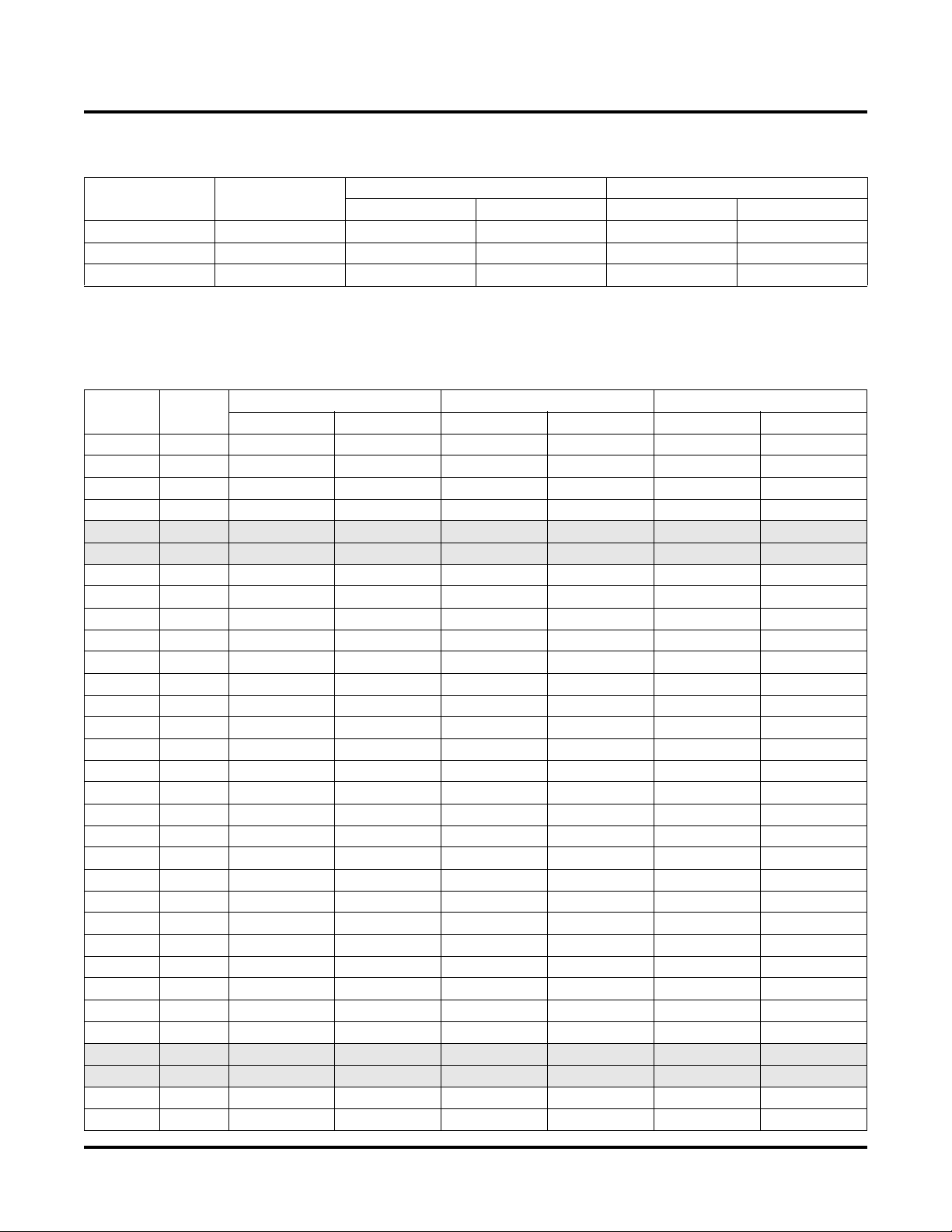
Lattice Semiconductor ispMACH 4000V/B/C/Z Family Data Sheet
ispMACH 4032V/B/C and 4064V/B/C Logic Signal Connections:
44-Pin TQFP (Cont.)
ispMACH 4032V/B/C ispMACH 4064V/B/C
Pin Number Bank Number
42 0 A2 A^2 A4 A^2
43 0 A3 A^3 A6 A^3
44 0 A4 A^4 A8 A^4
GLB/MC/Pad ORP GLB/MC/Pad ORP
ispMACH 4032V/B/C/Z and 4064V/B/C/Z Logic Signal Connections: 48-Pin TQFP
Pin
Number
1 - TDI - TDI - TDI -
2 0 A5 A^5 A10 A^5 A8 A^5
3 0 A6 A^6 A12 A^6 A10 A^6
4 0 A7 A^7 A14 A^7 A11 A^7
5 0 GND (Bank 0) - GND (Bank 0) - GND (Bank 0) -
6 0 VCCO (Bank 0) - VCCO (Bank 0) - VCCO (Bank 0) -
7 0 A8 A^8 B0 B^0 B15 B^7
8 0 A9 A^9 B2 B^1 B12 B^6
9 0 A10 A^10 B4 B^2 B10 B^5
10 0 A11 A^11 B6 B^3 B8 B^4
11 - TCK - TCK - TCK -
12 - VCC - VCC - VCC -
13 - GND - GND - GND -
14 0 A12 A^12 B8 B^4 B6 B^3
15 0 A13 A^13 B10 B^5 B4 B^2
16 0 A14 A^14 B12 B^6 B2 B^1
17 0 A15 A^15 B14 B^7 B0 B^0
18 0 CLK1/I - CLK1/I - CLK1/I -
19 1 CLK2/I - CLK2/I - CLK2/I -
20 1 B0 B^0 C0 C^0 C0 C^0
21 1 B1 B^1 C2 C^1 C1 C^1
22 1 B2 B^2 C4 C^2 C2 C^2
23 1 B3 B^3 C6 C^3 C4 C^3
24 1 B4 B^4 C8 C^4 C6 C^4
25 - TMS - TMS - TMS -
26 1 B5 B^5 C10 C^5 C8 C^5
27 1 B6 B^6 C12 C^6 C10 C^6
28 1 B7 B^7 C14 C^7 C11 C^7
29 1 GND (Bank 1) - GND (Bank 1) - GND (Bank 1) -
30 1 VCCO (Bank 1) - VCCO (Bank 1) - VCCO (Bank 1) -
31 1 B8 B^8 D0 D^0 D15 D^7
32 1 B9 B^9 D2 D^1 D12 D^6
Bank
Number
ispMACH 4032V/B/C/Z ispMACH 4064V/B/C ispMACH 4064Z
GLB/MC/Pad ORP GLB/MC/Pad ORP GLB/MC/Pad ORP
46
Page 47

Lattice Semiconductor ispMACH 4000V/B/C/Z Family Data Sheet
ispMACH 4032V/B/C/Z and 4064V/B/C/Z Logic Signal Connections:
48-Pin TQFP (Cont.)
Pin
Number
33 1 B10 B^10 D4 D^2 D10 D^5
34 1 B11 B^11 D6 D^3 D8 D^4
35 - TDO - TDO - TDO -
36 - VCC - VCC - VCC -
37 - GND - GND - GND -
38 1 B12 B^12 D8 D^4 D6 D^3
39 1 B13 B^13 D10 D^5 D4 D^2
40 1 B14 B^14 D12 D^6 D2 D^1
41 1 B15/GOE1 B^15 D14/GOE1 D^7 D0/GOE1 D^0
42 1 CLK3/I - CLK3/I - CLK3/I -
43 0 CLK0/I - CLK0/I - CLK0/I -
44 0 A0/GOE0 A^0 A0/GOE0 A^0 A0/GOE0 A^0
450A1A^1A2A^1A1A^1
460A2A^2A4A^2A2A^2
470A3A^3A6A^3A4A^3
480A4A^4A8A^4A6A^4
Bank
Number
ispMACH 4032V/B/C/Z ispMACH 4064V/B/C ispMACH 4064Z
GLB/MC/Pad ORP GLB/MC/Pad ORP GLB/MC/Pad ORP
ispMACH 4032Z and 4064Z Logic Signal Connections: 56-Ball csBGA
ispMACH 4032Z ispMACH 4064Z
Ball Number Bank Number
B1 -TDI-TDI-
C3 0 A5 A^5 A8 A^5
C1 0 A6 A^6 A10 A^6
D1 0 A7 A^7 A11 A^7
D3 0 GND (Bank 0) - GND (Bank 0) -
E3 0 NC
E1 0 NC
F3 0 VCCO (Bank 0) - VCCO (Bank 0) -
F1 0 A8 A^8 B15 B^7
G3 0 A9 A^9 B12 B^6
G1 0 A10 A^10 B10 B^5
H1 0 A11 A^11 B8 B^4
J1 0 NC - I -
K1 -TCK-TCK-
K2 -VCC-VCC-
H3 - GND - GND -
K3 - NC
K4 0 A12 A^12 B6 B^3
H4 0 A13 A^13 B4 B^2
H5 0 A14 A^14 B2 B^1
GLB/MC/Pad ORP GLB/MC/Pad ORP
1
1
1
-I1-
-I1-
-I1-
47
Page 48

Lattice Semiconductor ispMACH 4000V/B/C/Z Family Data Sheet
ispMACH 4032Z and 4064Z Logic Signal Connections: 56-Ball csBGA (Cont.)
ispMACH 4032Z ispMACH 4064Z
Ball Number Bank Number
K5 0 A15 A^15 B0 B^0
H6 0 CLK1/I - CLK1/I -
K6 1 CLK2/I - CLK2/I -
H7 1 B0 B^0 C0 C^0
K7 1 B1 B^1 C1 C^1
K8 1 B2 B^2 C2 C^2
K9 1 B3 B^3 C4 C^3
K10 1 B4 B^4 C6 C^4
J10 - TMS - TMS -
H8 1 B5 B^5 C8 C^5
H10 1 B6 B^6 C10 C^6
G10 1 B7 B^7 C11 C^7
G8 1 GND (Bank 1) - GND (Bank 1) -
F8 1 NC
F10 1 NC
E8 1 VCCO (Bank 1) - VCCO (Bank 1) -
E10 1 B8 B^8 D15 D^7
D8 1 B9 B^9 D12 D^6
D10 1 B10 B^10 D10 D^5
C10 1 B11 B^11 D8 D^4
B10 1 NC
A10 - TDO - TDO -
A9 -VCC-VCC-
C8 - GND - GND -
A8 1 NC
A7 1 B12 B^12 D6 D^3
C7 1 B13 B^13 D4 D^2
C6 1 B14 B^14 D2 D^1
A6 1 B15/GOE1 B^15 D0/GOE1 D^0
C5 1 CLK3/I - CLK3/I -
A5 0 CLK0/I - CLK0/I -
C4 0 A0/GOE0 A^0 A0/GOE0 A^0
A4 0 A1 A^1 A1 A^1
A3 0 A2 A^2 A2 A^2
A2 0 A3 A^3 A4 A^3
A1 0 A4 A^4 A6 A^4
1. For device migration considerations, these NC pins are input signal pins in ispMACH 4064Z devices.
GLB/MC/Pad ORP GLB/MC/Pad ORP
1
1
1
1
-I1-
-I1-
-I1-
-I1-
48
Page 49

Lattice Semiconductor ispMACH 4000V/B/C/Z Family Data Sheet
ispMACH 4064V/B/C/Z, 4128V/B/C/Z, 4256V/B/C/Z Logic Signal Connections: 100-Pin TQFP
Bank
Pin Number
1 - GND - GND - GND -
2 - TDI - TDI - TDI -
3 0 A8 A^8 B0 B^0 C12 C^3
4 0 A9 A^9 B2 B^1 C10 C^2
5 0 A10 A^10 B4 B^2 C6 C^1
6 0 A11 A^11 B6 B^3 C2 C^0
7 0 GND (Bank 0) - GND (Bank 0) - GND (Bank 0) -
8 0 A12 A^12 B8 B^4 D12 D^3
9 0 A13A^13B10 B^5 D10 D^2
10 0 A14 A^14 B12 B^6 D6 D^1
11 0 A15 A^15 B13 B^7 D4 D^0
12* 0 I - I - I -
13 0 VCCO (Bank 0) - VCCO (Bank 0) - VCCO (Bank 0) -
14 0 B15 B^15 C14 C^7 E4 E^0
15 0 B14 B^14 C12 C^6 E6 E^1
16 0 B13 B^13 C10 C^5 E10 E^2
17 0 B12 B^12 C8 C^4 E12 E^3
18 0 GND (Bank 0) - GND (Bank 0) - GND (Bank 0) -
19 0 B11 B^11 C6 C^3 F2 F^0
20 0 B10 B^10 C5 C^2 F6 F^1
21 0 B9 B^9 C4 C^1 F10 F^2
22 0 B8 B^8 C2 C^0 F12 F^3
23*0I-I-I-
24 - TCK - TCK - TCK -
25 - VCC - VCC - VCC -
26 - GND - GND - GND -
27*0I-I-I-
28 0 B7 B^7 D13 D^7 G12 G^3
29 0 B6 B^6 D12 D^6 G10 G^2
30 0 B5 B^5 D10 D^5 G6 G^1
31 0 B4 B^4 D8 D^4 G2 G^0
32 0 GND (Bank 0) - GND (Bank 0) - GND (Bank 0) -
33 0 VCCO (Bank 0) - VCCO (Bank 0) - VCCO (Bank 0) -
34 0 B3 B^3 D6 D^3 H12 H^3
35 0 B2 B^2 D4 D^2 H10 H^2
36 0 B1 B^1 D2 D^1 H6 H^1
37 0 B0 B^0 D0 D^0 H2 H^0
38 0 CLK1/I - CLK1/I - CLK1/I -
39 1 CLK2/I - CLK2/I - CLK2/I -
40 - VCC - VCC - VCC -
41 1 C0 C^0 E0 E^0 I2 I^0
Number
ispMACH 4064V/B/C/Z ispMACH 4128V/B/C/Z ispMACH 4256V/B/C/Z
GLB/MC/Pad ORP GLB/MC/Pad ORP GLB/MC/Pad ORP
49
Page 50

Lattice Semiconductor ispMACH 4000V/B/C/Z Family Data Sheet
ispMACH 4064V/B/C/Z, 4128V/B/C/Z, 4256V/B/C/Z Logic Signal Connections:
100-Pin TQFP (Cont.)
Bank
Pin Number
42 1 C1 C^1 E2 E^1 I6 I^1
43 1 C2 C^2 E4 E^2 I10 I^2
44 1 C3 C^3 E6 E^3 I12 I^3
45 1 VCCO (Bank 1) - VCCO (Bank 1) - VCCO (Bank 1) -
46 1 GND (Bank 1) - GND (Bank 1) - GND (Bank 1) -
47 1 C4 C^4 E8 E^4 J2 J^0
48 1 C5 C^5 E10 E^5 J6 J^1
49 1 C6 C^6 E12 E^6 J10 J^2
50 1 C7 C^7 E14 E^7 J12 J^3
51 - GND - GND - GND -
52 - TMS - TMS - TMS -
53 1 C8 C^8 F0 F^0 K12 K^3
54 1 C9 C^9 F2 F^1 K10 K^2
55 1 C10 C^10 F4 F^2 K6 K^1
56 1 C11 C^11 F6 F^3 K2 K^0
57 1 GND (Bank 1) - GND (Bank 1) - GND (Bank 1) -
58 1 C12 C^12 F8 F^4 L12 L^3
59 1 C13 C^13 F10 F^5 L10 L^2
60 1 C14 C^14 F12 F^6 L6 L^1
61 1 C15 C^15 F13 F^7 L4 L^0
62*1I-I-I-
63 1 VCCO (Bank 1) - VCCO (Bank 1) - VCCO (Bank 1) -
64 1 D15 D^15 G14 G^7 M4 M^0
65 1 D14 D^14 G12 G^6 M6 M^1
66 1 D13 D^13 G10 G^5 M10 M^2
67 1 D12 D^12 G8 G^4 M12 M^3
68 1 GND (Bank 1) - GND (Bank 1) - GND (Bank 1) -
69 1 D11 D^11 G6 G^3 N2 N^0
70 1 D10 D^10 G5 G^2 N6 N^1
71 1 D9 D^9 G4 G^1 N10 N^2
72 1 D8 D^8 G2 G^0 N12 N^3
73*1I-I-I-
74 - TDO - TDO - TDO -
75 - VCC - VCC - VCC -
76 - GND - GND - GND -
77*1I-I-I-
78 1 D7 D^7 H13 H^7 O12 O^3
79 1 D6 D^6 H12 H^6 O10 O^2
80 1 D5 D^5 H10 H^5 O6 O^1
81 1 D4 D^4 H8 H^4 O2 O^0
82 1 GND (Bank 1) - GND (Bank 1) - GND (Bank 1) -
Number
ispMACH 4064V/B/C/Z ispMACH 4128V/B/C/Z ispMACH 4256V/B/C/Z
GLB/MC/Pad ORP GLB/MC/Pad ORP GLB/MC/Pad ORP
50
Page 51

Lattice Semiconductor ispMACH 4000V/B/C/Z Family Data Sheet
ispMACH 4064V/B/C/Z, 4128V/B/C/Z, 4256V/B/C/Z Logic Signal Connections:
100-Pin TQFP (Cont.)
Bank
Pin Number
83 1 VCCO (Bank 1) - VCCO (Bank 1) - VCCO (Bank 1) -
84 1 D3 D^3 H6 H^3 P12 P^3
85 1 D2 D^2 H4 H^2 P10 P^2
86 1 D1 D^1 H2 H^1 P6 P^1
87 1 D0/GOE1 D^0 H0/GOE1 H^0 P2/OE1 P^0
88 1 CLK3/I - CLK3/I - CLK3/I -
89 0 CLK0/I - CLK0/I - CLK0/I -
90 - VCC - VCC - VCC -
91 0 A0/GOE0 A^0 A0/GOE0 A^0 A2/GOE0 A^0
92 0 A1 A^1 A2 A^1 A6 A^1
93 0 A2 A^2 A4 A^2 A10 A^2
94 0 A3 A^3 A6 A^3 A12 A^3
95 0 VCCO (Bank 0) - VCCO (Bank 0) - VCCO (Bank 0) -
96 0 GND (Bank 0) - GND (Bank 0) - GND (Bank 0) -
97 0 A4 A^4 A8 A^4 B2 B^0
98 0 A5 A^5 A10 A^5 B6 B^1
99 0 A6 A^6 A12 A^6 B10 B^2
100 0 A7 A^7 A14 A^7 B12 B^3
*This pin is input only.
Number
ispMACH 4064V/B/C/Z ispMACH 4128V/B/C/Z ispMACH 4256V/B/C/Z
GLB/MC/Pad ORP GLB/MC/Pad ORP GLB/MC/Pad ORP
ispMACH 4128V/B/C Logic Signal Connections: 128-Pin TQFP
ispMACH 4128V/B/C
Pin Number Bank Number
10GND-
20TDI-
3 0 VCCO (Bank 0) -
4 0 B0 B^0
5 0 B1 B^1
6 0 B2 B^2
7 0 B4 B^3
8 0 B5 B^4
9 0 B6 B^5
10 0 GND (Bank 0) -
11 0 B8 B^6
12 0 B9 B^7
13 0 B10 B^8
14 0 B12 B^9
15 0 B13 B^10
16 0 B14 B^11
17 0 VCCO (Bank 0) -
18 0 C14 C^11
GLB/MC/Pad ORP
51
Page 52

Lattice Semiconductor ispMACH 4000V/B/C/Z Family Data Sheet
ispMACH 4128V/B/C Logic Signal Connections: 128-Pin TQFP (Cont.)
ispMACH 4128V/B/C
Pin Number Bank Number
19 0 C13 C^10
20 0 C12 C^9
21 0 C10 C^8
22 0 C9 C^7
23 0 C8 C^6
24 0 GND (Bank 0) -
25 0 C6 C^5
26 0 C5 C^4
27 0 C4 C^3
28 0 C2 C^2
29 0 C0 C^0
30 0 VCCO (Bank 0) -
31 0 TCK -
32 0 VCC -
33 0 GND -
34 0 D14 D^11
35 0 D13 D^10
36 0 D12 D^9
37 0 D10 D^8
38 0 D9 D^7
39 0 D8 D^6
40 0 GND (Bank 0) -
41 0 VCCO (Bank 0) -
42 0 D6 D^5
43 0 D5 D^4
44 0 D4 D^3
45 0 D2 D^2
46 0 D1 D^1
47 0 D0 D^0
48 0 CLK1/I -
49 1 GND (Bank 1) -
50 1 CLK2/I -
51 1 VCC -
52 1 E0 E^0
53 1 E1 E^1
54 1 E2 E^2
55 1 E4 E^3
56 1 E5 E^4
57 1 E6 E^5
58 1 VCCO (Bank 1) -
59 1 GND (Bank 1) -
60 1 E8 E^6
61 1 E9 E^7
GLB/MC/Pad ORP
52
Page 53

Lattice Semiconductor ispMACH 4000V/B/C/Z Family Data Sheet
ispMACH 4128V/B/C Logic Signal Connections: 128-Pin TQFP (Cont.)
ispMACH 4128V/B/C
Pin Number Bank Number
62 1 E10 E^8
63 1 E12 E^9
64 1 E14 E^11
65 1 GND -
66 1 TMS -
67 1 VCCO (Bank 1) -
68 1 F0 F^0
69 1 F1 F^1
70 1 F2 F^2
71 1 F4 F^3
72 1 F5 F^4
73 1 F6 F^5
74 1 GND (Bank 1) -
75 1 F8 F^6
76 1 F9 F^7
77 1 F10 F^8
78 1 F12 F^9
79 1 F13 F^10
80 1 F14 F^11
81 1 VCCO (Bank 1) -
82 1 G14 G^11
83 1 G13 G^10
84 1 G12 G^9
85 1 G10 G^8
86 1 G9 G^7
87 1 G8 G^6
88 1 GND (Bank 1) -
89 1 G6 G^5
90 1 G5 G^4
91 1 G4 G^3
92 1 G2 G^2
93 1 G0 G^0
94 1 VCCO (Bank 1) -
95 1 TDO -
96 1 VCC -
97 1 GND -
98 1 H14 H^11
99 1 H13 H^10
100 1 H12 H^9
101 1 H10 H^8
102 1 H9 H^7
103 1 H8 H^6
104 1 GND (Bank 1) -
GLB/MC/Pad ORP
53
Page 54

Lattice Semiconductor ispMACH 4000V/B/C/Z Family Data Sheet
ispMACH 4128V/B/C Logic Signal Connections: 128-Pin TQFP (Cont.)
ispMACH 4128V/B/C
Pin Number Bank Number
105 1 VCCO (Bank 1) -
106 1 H6 H^5
107 1 H5 H^4
108 1 H4 H^3
109 1 H2 H^2
110 1 H1 H^1
111 1 H0/GOE1 H^0
112 1 CLK3/I -
113 0 GND (Bank 0) -
114 0 CLK0/I -
115 0 VCC -
116 0 A0/GOE0 A^0
117 0 A1 A^1
118 0 A2 A^2
119 0 A4 A^3
120 0 A5 A^4
121 0 A6 A^5
122 0 VCCO (Bank 0) -
123 0 GND (Bank 0) -
124 0 A8 A^6
125 0 A9 A^7
126 0 A10 A^8
127 0 A12 A^9
128 0 A14 A^11
GLB/MC/Pad ORP
ispMACH 4064Z, 4128Z and 4256Z Logic Signal Connections: 132-Ball csBGA
ispMACH 4064Z ispMACH 4128Z ispMACH 4256Z
Ball Number Bank Number
B1 -GND-GND-GND-
B2 -TDI-TDI-TDI-
C1 0 NC - VCCO (Bank 0) - VCCO (Bank 0) -
C3 0 NC - B0 B^0 C12 C^6
C2 0 A8 A^8 B1 B^1 C10 C^5
D1 0 A9 A^9 B2 B^2 C8 C^4
D3 0 A10 A^10 B4 B^3 C6 C^3
D2 0 A11 A^11 B5 B^4 C4 C^2
E1 0 NC B6 B^5 C2 C^1
E2 0 GND (Bank 0) - GND (Bank 0) - GND (Bank 0) -
GLB/MC/Pad ORP GLB/MC/Pad ORP GLB/MC/Pad ORP
54
Page 55

Lattice Semiconductor ispMACH 4000V/B/C/Z Family Data Sheet
ispMACH 4064Z, 4128Z and 4256Z Logic Signal Connections:
132-Ball csBGA (Cont.)
ispMACH 4064Z ispMACH 4128Z ispMACH 4256Z
Ball Number Bank Number
E3 0 NC - B8 B^6 D12 D^6
F2 0 A12 A^12 B9 B^7 D10 D^5
F1 0 A13 A^13 B10 B^8 D8 D^4
F3 0 A14 A^14 B12 B^9 D6 D^3
G1 0 A15 A^15 B13 B^10 D4 D^2
G2 0 I - B14 B^11 D2 D^1
G3 0 VCCO (Bank 0) - VCCO (Bank 0) - VCCO (Bank 0) -
H2 0 NC - C14 C^11 E2 E^1
H1 0 B15 B^15 C13 C^10 E4 E^2
H3 0 B14 B^14 C12 C^9 E6 E^3
J1 0 B13 B^13 C10 C^8 E8 E^4
J2 0 B12 B^12 C9 C^7 E10 E^5
J3 0 NC - C8 C^6 E12 E^6
K2 0 GND (Bank 0) - GND (Bank 0) - GND (Bank 0) -
K1 0 NC - C6 C^5 F2 F^1
K3 0 B11 B^11 C5 C^4 F4 F^2
L2 0 B10 B^10 C4 C^3 F6 F^3
L1 0 B9 B^9 C2 C^2 F8 F^4
L3 0 B8 B^8 C1 C^1 F10 F^5
M1 0 I - C0 C^0 F12 F^6
M2 0 NC - VCCO (Bank 0) - VCCO (Bank 0) -
N1 - TCK - TCK - TCK -
P1 -VCC-VCC-VCC-
P2 -GND-GND-GND-
N2 0 I - D14 D^11 G12 G^6
P3 0 B7 B^7 D13 D^10 G10 G^5
M3 0 B6 B^6 D12 D^9 G8 G^4
N3 0 B5 B^5 D10 D^8 G6 G^3
P4 0 B4 B^4 D9 D^7 G4 G^2
M4 0 NC - D8 D^6 G2 G^1
N4 0 GND (Bank 0) - GND (Bank 0) - GND (Bank 0) -
P5 0 VCCO (Bank 0) - VCCO (Bank 0) - VCCO (Bank 0) -
N5 0 NC - D6 D^5 H12 H^6
M5 0 B3 B^3 D5 D^4 H10 H^5
N6 0 B2 B^2 D4 D^3 H8 H^4
P6 0 B1 B^1 D2 D^2 H6 H^3
M6 0 B0 B^0 D1 D^1 H4 H^2
P7 0 NC - D0 D^0 H2 H^1
N7 0 CLK1/I - CLK1/I - CLK1/I -
M7 1 CLK2/I - CLK2/I - CLK2/I -
N8 - VCC - VCC - VCC -
GLB/MC/Pad ORP GLB/MC/Pad ORP GLB/MC/Pad ORP
55
Page 56

Lattice Semiconductor ispMACH 4000V/B/C/Z Family Data Sheet
ispMACH 4064Z, 4128Z and 4256Z Logic Signal Connections:
132-Ball csBGA (Cont.)
ispMACH 4064Z ispMACH 4128Z ispMACH 4256Z
Ball Number Bank Number
P8 1 NC
M8 1 NC - E0 E^0 I2 I^1
P9 1 C0 C^0 E1 E^1 I4 I^2
N9 1 C1 C^1 E2 E^2 I6 I^3
M9 1 C2 C^2 E4 E^3 I8 I^4
N10 1 C3 C^3 E5 E^4 I10 I^5
P10 1 NC - E6 E^5 I12 I^6
M10 1 VCCO (Bank 1) - VCCO (Bank 1) - VCCO (Bank 1) -
N11 1 GND (Bank 1) - GND (Bank 1) - GND (Bank 1) -
P11 1 NC - E8 E^6 J2 J^1
M11 1 C4 C^4 E9 E^7 J4 J^2
P12 1 C5 C^5 E10 E^8 J6 J^3
N12 1 C6 C^6 E12 E^9 J8 J^4
P13 1 C7 C^7 E13 E^10 J10 J^5
P14 1 NC - E14 E^11 J12 J^6
N14 - GND - GND - GND -
N13 - TMS - TMS - TMS -
M14 1 NC - VCCO (Bank 1) - VCCO (Bank 1) -
M12 1 NC - F0 F^0 K12 K^6
M13 1 C8 C^8 F1 F^1 K10 K^5
L14 1 C9 C^9 F2 F^2 K8 K^4
L12 1 C10 C^10 F4 F^3 K6 K^3
L13 1 C11 C^11 F5 F^4 K4 K^2
K14 1 NC - F6 F^5 K2 K^1
K13 1 GND (Bank 1) - GND (Bank 1) - GND (Bank 1) -
K12 1 NC - F8 F^6 L12 L^6
J13 1 C12 C^12 F9 F^7 L10 L^5
J14 1 C13 C^13 F10 F^8 L8 L^4
J12 1 C14 C^14 F12 F^9 L6 L^3
H14 1 C15 C^15 F13 F^10 L4 L^2
H13 1 I - F14 F^11 L2 L^1
H12 1 VCCO (Bank 1) - VCCO (Bank 1) - VCCO (Bank 1) -
G13 1 NC - G14 G^11 M2 M^1
G14 1 NC - G13 G^10 M4 M^2
G12 1 D15 D^15 G12 G^9 M6 M^3
F14 1 D14 D^14 G10 G^8 M8 M^4
F13 1 D13 D^13 G9 G^7 M10 M^5
F12 1 D12 D^12 G8 G^6 M12 M^6
E13 1 GND (Bank 1) - GND (Bank 1) - GND (Bank 1) -
E14 1 NC - G6 G^5 N2 N^1
E12 1 D11 D^11 G5 G^4 N4 N^2
GLB/MC/Pad ORP GLB/MC/Pad ORP GLB/MC/Pad ORP
1
-NC1-I1-
56
Page 57

Lattice Semiconductor ispMACH 4000V/B/C/Z Family Data Sheet
ispMACH 4064Z, 4128Z and 4256Z Logic Signal Connections:
132-Ball csBGA (Cont.)
ispMACH 4064Z ispMACH 4128Z ispMACH 4256Z
Ball Number Bank Number
D13 1 D10 D^10 G4 G^3 N6 N^3
D14 1 D9 D^9 G2 G^2 N8 N^4
D12 1 D8 D^8 G1 G^1 N10 N^5
C14 1 I - G0 G^0 N12 N^6
C13 1 NC - VCCO (Bank 1) - VCCO (Bank 1) -
B14 - TDO - TDO - TDO -
A14 - VCC - VCC - VCC -
A13 - GND - GND - GND -
B13 1 NC - H14 H^11 O12 O^6
A12 1 I - H13 H^10 O10 O^5
C12 1 D7 D^7 H12 H^9 O8 O^4
B12 1 D6 D^6 H10 H^8 O6 O^3
A11 1 D5 D^5 H9 H^7 O4 O^2
C11 1 D4 D^4 H8 H^6 O2 O^1
B11 1 GND (Bank 1) - GND (Bank 1) - GND (Bank 1) -
A10 1 VCCO (Bank 1) - VCCO (Bank 1) - VCCO (Bank 1) -
B10 1 NC - H6 H^5 P12 P^6
C10 1 NC - H5 H^4 P10 P^5
B9 1 D3 D^3 H4 H^3 P8 P^4
A9 1 D2 D^2 H2 H^2 P6 P^3
C9 1 D1 D^1 H1 H^1 P4 P^2
A8 1 D0/GOE1 D^0 H0/GOE1 H^0 P2/GOE1 P^1
B8 1 CLK3/I - CLK3/I - CLK3/I -
C8 0 CLK0/I - CLK0/I - CLK0/I -
B7 -VCC-VCC-VCC-
A7 0 NC
C7 0 A0/GOE0 A^0 A0/GOE0 A^0 A2/GOE0 A^1
A6 0 A1 A^1 A1 A^1 A4 A^2
B6 0 A2 A^2 A2 A^2 A6 A^3
C6 0 A3 A^3 A4 A^3 A8 A^4
B5 0 NC - A5 A^4 A10 A^5
A5 0 NC - A6 A^5 A12 A^6
C5 0 VCCO (Bank 0) - VCCO (Bank 0) - VCCO (Bank 0) -
B4 0 GND (Bank 0) - GND (Bank 0) - GND (Bank 0) -
A4 0 NC - A8 A^6 B2 B^1
C4 0 A4 A^4 A9 A^7 B4 B^2
A3 0 A5 A^5 A10 A^8 B6 B^3
B3 0 A6 A^6 A12 A^9 B8 B^4
A2 0 A7 A^7 A13 A^10 B10 B^5
A1 0 NC - A14 A^11 B12 B^6
1. For device migration considerations, these NC pins are input signal pins in ispMACH 4256Z device.
GLB/MC/Pad ORP GLB/MC/Pad ORP GLB/MC/Pad ORP
1
-NC1-I1-
57
Page 58

Lattice Semiconductor ispMACH 4000V/B/C/Z Family Data Sheet
ispMACH 4128V and 4256V Logic Signal Connections: 144-Pin TQFP
ispMACH 4128V ispMACH 4256V
Pin Number Bank Number
1 - GND - GND -
2 - TDI - TDI -
3 0 VCCO (Bank 0) - VCCO (Bank 0) -
4 0 B0 B^0 C12 C^6
5 0 B1 B^1 C10 C^5
6 0 B2 B^2 C8 C^4
7 0 B4 B^3 C6 C^3
8 0 B5 B^4 C4 C^2
9 0 B6 B^5 C2 C^1
10 0 GND (Bank 0) - GND (Bank 0) -
11 0 B8 B^6 D14 D^7
12 0 B9 B^7 D12 D^6
13 0 B10 B^8 D10 D^5
14 0 B12 B^9 D8 D^4
15 0 B13 B^10 D6 D^3
16 0 B14 B^11 D4 D^2
17 - NC
18 0 GND (Bank 0)
19 0 VCCO (Bank 0) - VCCO (Bank 0) -
20 0 NC
21 0 C14 C^11 E2 E^1
22 0 C13 C^10 E4 E^2
23 0 C12 C^9 E6 E^3
24 0 C10 C^8 E8 E^4
25 0 C9 C^7 E10 E^5
26 0 C8 C^6 E12 E^6
27 0 GND (Bank 0) - GND (Bank 0) -
28 0 C6 C^5 F2 F^1
29 0 C5 C^4 F4 F^2
30 0 C4 C^3 F6 F^3
31 0 C2 C^2 F8 F^4
32 0 C1 C^1 F10 F^5
33 0 C0 C^0 F12 F^6
34 0 VCCO (Bank 0) - VCCO (Bank 0) -
35 -TCK-TCK-
36 - VCC - VCC -
37 -GND-GND-
38 0 NC
39 0 D14 D^11 G12 G^6
40 0 D13 D^10 G10 G^5
41 0 D12 D^9 G8 G^4
42 0 D10 D^8 G6 G^3
GLB/MC/Pad ORP GLB/MC/Pad ORP
2
1
2
2
-I2-
- NC
1
-I2-
-I2-
-
58
Page 59

Lattice Semiconductor ispMACH 4000V/B/C/Z Family Data Sheet
ispMACH 4128V and 4256V Logic Signal Connections: 144-Pin TQFP (Cont.)
ispMACH 4128V ispMACH 4256V
Pin Number Bank Number
43 0 D9 D^7 G4 G^2
44 0 D8 D^6 G2 G^1
45 0 NC
46 0 GND (Bank 0) - GND (Bank 0) -
47 0 VCCO (Bank 0) - VCCO (Bank 0) -
48 0 D6 D^5 H12 H^6
49 0 D5 D^4 H10 H^5
50 0 D4 D^3 H8 H^4
51 0 D2 D^2 H6 H^3
52 0 D1 D^1 H4 H^2
53 0 D0 D^0 H2 H^1
54 0 CLK1/I - CLK1/I -
55 1 GND (Bank 1) - GND (Bank 1) -
56 1 CLK2/I - CLK2/I -
57 -VCC-VCC-
58 1 E0 E^0 I2 I^1
59 1 E1 E^1 I4 I^2
60 1 E2 E^2 I6 I^3
61 1 E4 E^3 I8 I^4
62 1 E5 E^4 I10 I^5
63 1 E6 E^5 I12 I^6
64 1 VCCO (Bank 1) - VCCO (Bank 1) -
65 1 GND (Bank 1) - GND (Bank 1) -
66 1 E8 E^6 J2 J^1
67 1 E9 E^7 J4 J^2
68 1 E10 E^8 J6 J^3
69 1 E12 E^9 J8 J^4
70 1 E13 E^10 J10 J^5
71 1 E14 E^11 J12 J^6
72 1 NC
73 -GND-GND-
74 -TMS-TMS-
75 1 VCCO (Bank 1) - VCCO (Bank 1) -
76 1 F0 F^0 K12 K^6
77 1 F1 F^1 K10 K^5
78 1 F2 F^2 K8 K^4
79 1 F4 F^3 K6 K^3
80 1 F5 F^4 K4 K^2
81 1 F6 F^5 K2 K^1
82 1 GND (Bank 1) - GND (Bank 1) -
83 1 F8 F^6 L14 L^7
84 1 F9 F^7 L12 L^6
85 1 F10 F^8 L10 L^5
GLB/MC/Pad ORP GLB/MC/Pad ORP
2
2
-I2-
-I2-
59
Page 60
Lattice Semiconductor ispMACH 4000V/B/C/Z Family Data Sheet
ispMACH 4128V and 4256V Logic Signal Connections: 144-Pin TQFP (Cont.)
ispMACH 4128V ispMACH 4256V
Pin Number Bank Number
86 1 F12 F^9 L8 L^4
87 1 F13 F^10 L6 L^3
88 1 F14 F^11 L4 L^2
89 1 NC
90 1 GND (Bank 1)
91 1 VCCO (Bank 1) - VCCO (Bank 1) -
92 1 NC
93 1 G14 G^11 M2 M^1
94 1 G13 G^10 M4 M^2
95 1 G12 G^9 M6 M^3
96 1 G10 G^8 M8 M^4
97 1 G9 G^7 M10 M^5
98 1 G8 G^6 M12 M^6
99 1 GND (Bank 1) - GND (Bank 1) -
100 1 G6 G^5 N2 N^1
101 1 G5 G^4 N4 N^2
102 1 G4 G^3 N6 N^3
103 1 G2 G^2 N8 N^4
104 1 G1 G^1 N10 N^5
105 1 G0 G^0 N12 N^6
106 1 VCCO (Bank 1) - VCCO (Bank 1) -
107 -TDO-TDO-
108 -VCC-VCC-
109 -GND-GND-
110 1 NC
111 1 H14 H^11 O12 O^6
112 1 H13 H^10 O10 O^5
113 1 H12 H^9 O8 O^4
114 1 H10 H^8 O6 O^3
115 1 H9 H^7 O4 O^2
116 1 H8 H^6 O2 O^1
117 1 NC
118 1 GND (Bank 1) - GND (Bank 1) -
119 1 VCCO (Bank 1) - VCCO (Bank 1) -
120 1 H6 H^5 P12 P^6
121 1 H5 H^4 P10 P^5
122 1 H4 H^3 P8 P^4
123 1 H2 H^2 P6 P^3
124 1 H1 H^1 P4 P^2
125 1 H0/GOE1 H^0 P2/GOE1 P^1
126 1 CLK3/I - CLK3/I -
127 0 GND (Bank 0) - GND (Bank 0) -
128 0 CLK0/I - CLK0/I -
GLB/MC/Pad ORP GLB/MC/Pad ORP
2
1
2
2
2
-I2-
- NC
1
-I2-
-I2-
-I2-
-
60
Page 61

Lattice Semiconductor ispMACH 4000V/B/C/Z Family Data Sheet
ispMACH 4128V and 4256V Logic Signal Connections: 144-Pin TQFP (Cont.)
ispMACH 4128V ispMACH 4256V
Pin Number Bank Number
129 -VCC-VCC-
130 0 A0/GOE0 A^0 A2/GOE0 A^1
131 0 A1 A^1 A4 A^2
132 0 A2 A^2 A6 A^3
133 0 A4 A^3 A8 A^4
134 0 A5 A^4 A10 A^5
135 0 A6 A^5 A12 A^6
136 0 VCCO (Bank 0) - VCCO (Bank 0) -
137 0 GND (Bank 0) - GND (Bank 0) -
138 0 A8 A^6 B2 B^1
139 0 A9 A^7 B4 B^2
140 0 A10 A^8 B6 B^3
141 0 A12 A^9 B8 B^4
142 0 A13 A^10 B10 B^5
143 0 A14 A^11 B12 B^6
144 0 NC
1. For device migration considerations, these NC pins are GND pins for I/O banks in ispMACH 4128V devices.
2. For device migration considerations, these NC pins are input signal pins in ispMACH 4256V devices.
GLB/MC/Pad ORP GLB/MC/Pad ORP
2
-I2-
ispMACH 4256V/B/C/Z, 4384V/B/C, 4512V/B/C, Logic Signal Connections: 176-Pin TQFP
Pin Number
1 - NC - NC - NC -
2 - GND-GND-GND -
3 - TDI - TDI - TDI -
4 0 VCCO (Bank 0) - VCCO (Bank 0) - VCCO (Bank 0) -
5 0 C14 C^7 C14 C^7 C14 C^7
6 0 C12 C^6 C12 C^6 C12 C^6
7 0 C10 C^5 C10 C^5 C10 C^5
8 0 C8 C^4 C8 C^4 C8 C^4
9 0 C6 C^3 C6 C^3 C6 C^3
10 0 C4 C^2 C4 C^2 C4 C^2
11 0 C2 C^1 C2 C^1 C2 C^1
12 0 C0 C^0 C0 C^0 C0 C^0
13 0 GND (Bank 0) - GND (Bank 0) - GND (Bank 0) -
14 0 D14 D^7 E14 E^7 G14 G^7
15 0 D12 D^6 E12 E^6 G12 G^6
16 0 D10 D^5 E10 E^5 G10 G^5
17 0 D8 D^4 E8 E^4 G8 G^4
18 0 D6 D^3 E6 E^3 G6 G^3
Bank
Number
ispMACH 4256V/B/C/Z ispMACH 4384V/B/C ispMACH 4512V/B/C
GLB/MC/Pad ORP GLB/MC/Pad ORP GLB/MC/Pad ORP
61
Page 62

Lattice Semiconductor ispMACH 4000V/B/C/Z Family Data Sheet
ispMACH 4256V/B/C/Z, 4384V/B/C, 4512V/B/C, Logic Signal Connections:
176-Pin TQFP (Cont.)
Bank
Pin Number
19 0 D4 D^2 E4 E^2 G4 G^2
20 0 D2 D^1 E2 E^1 G2 G^1
21 0 D0 D^0 E0 E^0 G0 G^0
22 0 VCCO (Bank 0) - VCCO (Bank 0) - VCCO (Bank 0) -
23 0 E0 E^0 H0 H^0 J0 J^0
24 0 E2 E^1 H2 H^1 J2 J^1
25 0 E4 E^2 H4 H^2 J4 J^2
26 0 E6 E^3 H6 H^3 J6 J^3
27 0 E8 E^4 H8 H^4 J8 J^4
28 0 E10 E^5 H10 H^5 J10 J^5
29 0 E12 E^6 H12 H^6 J12 J^6
30 0 E14 E^7 H14 H^7 J14 J^7
31 0 GND (Bank 0) - GND (Bank 0) - GND (Bank 0) -
32 0 F0 F^0 J0 J^0 N0 N^0
33 0 F2 F^1 J2 J^1 N2 N^1
34 0 F4 F^2 J4 J^2 N4 N^2
35 0 F6 F^3 J6 J^3 N6 N^3
36 0 F8 F^4 J8 J^4 N8 N^4
37 0 F10 F^5 J10 J^5 N10 N^5
38 0 F12 F^6 J12 J^6 N12 N^6
39 0 F14 F^7 J14 J^7 N14 N^7
40 0 VCCO (Bank 0) - VCCO (Bank 0) - VCCO (Bank 0) -
41 - TCK - TCK - TCK -
42 - VCC - VCC - VCC -
43 - NC - NC - NC -
44 - NC - NC - NC -
45 - NC - NC - NC -
46 - GND - GND (Bank 0) - GND -
47 0 G14 G^7 K14 K^7 O14 O^7
48 0 G12 G^6 K12 K^6 O12 O^6
49 0 G10 G^5 K10 K^5 O10 O^5
50 0 G8 G^4 K8 K^4 O8 O^4
51 0 G6 G^3 K6 K^3 O6 O^3
52 0 G4 G^2 K4 K^2 O4 O^2
53 0 G2 G^1 K2 K^1 O2 O^1
54 0 G0 G^0 K0 K^0 O0 O^0
55 0 GND (Bank 0) - GND (Bank 0) - GND (Bank 0) -
56 0 VCCO (Bank 0) - VCCO (Bank 0) - VCCO (Bank 0) -
57 0 H14 H^7 L14 L^7 P14 P^7
58 0 H12 H^6 L12 L^6 P12 P^6
59 0 H10 H^5 L10 L^5 P10 P^5
Number
ispMACH 4256V/B/C/Z ispMACH 4384V/B/C ispMACH 4512V/B/C
GLB/MC/Pad ORP GLB/MC/Pad ORP GLB/MC/Pad ORP
62
Page 63

Lattice Semiconductor ispMACH 4000V/B/C/Z Family Data Sheet
ispMACH 4256V/B/C/Z, 4384V/B/C, 4512V/B/C, Logic Signal Connections:
176-Pin TQFP (Cont.)
Bank
Pin Number
60 0 H8 H^4 L8 L^4 P8 P^4
61 0 H6 H^3 L6 L^3 P6 P^3
62 0 H4 H^2 L4 L^2 P4 P^2
63 0 H2 H^1 L2 L^1 P2 P^1
64 0 H0 H^0 L0 L^0 P0 P^0
65 - GND - GND - GND -
66 0 CLK1/I - CLK1/I - CLK1/I -
67 1 GND (Bank 1) - GND (Bank 1) - GND (Bank 1) -
68 1 CLK2/I - CLK2/I - CLK2/I -
69 - VCC - VCC - VCC -
70 1 I0 I^0 M0 M^0 AX0 AX^0
71 1 I2 I^1 M2 M^1 AX2 AX^1
72 1 I4 I^2 M4 M^2 AX4 AX^2
73 1 I6 I^3 M6 M^3 AX6 AX^3
74 1 I8 I^4 M8 M^4 AX8 AX^4
75 1 I10 I^5 M10 M^5 AX10 AX^5
76 1 I12 I^6 M12 M^6 AX12 AX^6
77 1 I14 I^7 M14 M^7 AX14 AX^7
78 1 VCCO (Bank 1) - VCCO (Bank 1) - VCCO (Bank 1) -
79 1 GND (Bank 1) - GND (Bank 1) - GND (Bank 1) -
80 1 J0 J^0 N0 N^0 BX0 BX^0
81 1 J2 J^1 N2 N^1 BX2 BX^1
82 1 J4 J^2 N4 N^2 BX4 BX^2
83 1 J6 J^3 N6 N^3 BX6 BX^3
84 1 J8 J^4 N8 N^4 BX8 BX^4
85 1 J10 J^5 N10 N^5 BX10 BX^5
86 1 J12 J^6 N12 N^6 BX12 BX^6
87 1 J14 J^7 N14 N^7 BX14 BX^7
88 - VCC - VCC - VCC -
89 - NC - NC - NC -
90 - GND - GND - GND -
91 - TMS - TMS - TMS -
92 1 VCCO (Bank 1) - VCCO (Bank 1) - VCCO (Bank 1) -
93 1 K14 K^7 O14 O^7 CX14 CX^7
94 1 K12 K^6 O12 O^6 CX12 CX^6
95 1 K10 K^5 O10 O^5 CX10 CX^5
96 1 K8 K^4 O8 O^4 CX8 CX^4
97 1 K6 K^3 O6 O^3 CX6 CX^3
98 1 K4 K^2 O4 O^2 CX4 CX^2
99 1 K2 K^1 O2 O^1 CX2 CX^1
100 1 K0 K^0 O0 O^0 CX0 CX^0
Number
ispMACH 4256V/B/C/Z ispMACH 4384V/B/C ispMACH 4512V/B/C
GLB/MC/Pad ORP GLB/MC/Pad ORP GLB/MC/Pad ORP
63
Page 64

Lattice Semiconductor ispMACH 4000V/B/C/Z Family Data Sheet
ispMACH 4256V/B/C/Z, 4384V/B/C, 4512V/B/C, Logic Signal Connections:
176-Pin TQFP (Cont.)
Bank
Pin Number
101 1 GND (Bank 1) - GND (Bank 1) - GND (Bank 1) -
102 1 L14 L^7 AX14 AX^7 GX14 GX^7
103 1 L12 L^6 AX12 AX^6 GX12 GX^6
104 1 L10 L^5 AX10 AX^5 GX10 GX^5
105 1 L8 L^4 AX8 AX^4 GX8 GX^4
106 1 L6 L^3 AX6 AX^3 GX6 GX^3
107 1 L4 L^2 AX4 AX^2 GX4 GX^2
108 1 L2 L^1 AX2 AX^1 GX2 GX^1
109 1 L0 L^0 AX0 AX^0 GX0 GX^0
110 1 VCCO (Bank 1) - VCCO (Bank 1) - VCCO (Bank 1) -
111 1 M0 M^0 DX0 DX^0 JX0 JX^0
112 1 M2 M^1 DX2 DX^1 JX2 JX^1
113 1 M4 M^2 DX4 DX^2 JX4 JX^2
114 1 M6 M^3 DX6 DX^3 JX6 JX^3
115 1 M8 M^4 DX8 DX^4 JX8 JX^4
116 1 M10 M^5 DX10 DX^5 JX10 JX^5
117 1 M12 M^6 DX12 DX^6 JX12 JX^6
118 1 M14 M^7 DX14 DX^7 JX14 JX^7
119 1 GND (Bank 1) - GND (Bank 1) - GND (Bank 1) -
120 1 N0 N^0 FX0 FX^0 NX0 NX^0
121 1 N2 N^1 FX2 FX^1 NX2 NX^1
122 1 N4 N^2 FX4 FX^2 NX4 NX^2
123 1 N6 N^3 FX6 FX^3 NX6 NX^3
124 1 N8 N^4 FX8 FX^4 NX8 NX^4
125 1 N10 N^5 FX10 FX^5 NX10 NX^5
126 1 N12 N^6 FX12 FX^6 NX12 NX^6
127 1 N14 N^7 FX14 FX^7 NX14 NX^7
128 1 VCCO (Bank 1) - VCCO (Bank 1) - VCCO (Bank 1) -
129 - TDO - TDO - TDO -
130 - VCC-VCC-VCC -
131 - NC - NC - NC -
132 - NC - NC - NC -
133 - NC - NC - NC -
134 - GND - GND - GND -
135 1 O14 O^7 GX14 GX^7 OX14 OX^7
136 1 O12 O^6 GX12 GX^6 OX12 OX^6
137 1 O10 O^5 GX10 GX^5 OX10 OX^5
138 1 O8 O^4 GX8 GX^4 OX8 OX^4
139 1 O6 O^3 GX6 GX^3 OX6 OX^3
140 1 O4 O^2 GX4 GX^2 OX4 OX^2
141 1 O2 O^1 GX2 GX^1 OX2 OX^1
Number
ispMACH 4256V/B/C/Z ispMACH 4384V/B/C ispMACH 4512V/B/C
GLB/MC/Pad ORP GLB/MC/Pad ORP GLB/MC/Pad ORP
64
Page 65

Lattice Semiconductor ispMACH 4000V/B/C/Z Family Data Sheet
ispMACH 4256V/B/C/Z, 4384V/B/C, 4512V/B/C, Logic Signal Connections:
176-Pin TQFP (Cont.)
Bank
Pin Number
142 1 O0 O^0 GX0 GX^0 OX0 OX^0
143 1 GND (Bank 1) - GND (Bank 1) - GND (Bank 1) -
144 1 VCCO (Bank 1) - VCCO (Bank 1) - VCCO (Bank 1) -
145 1 P14 P^7 HX14 HX^7 PX14 PX^7
146 1 P12 P^6 HX12 HX^6 PX12 PX^6
147 1 P10 P^5 HX10 HX^5 PX10 PX^5
148 1 P8 P^4 HX8 HX^4 PX8 PX^4
149 1 P6 P^3 HX6 HX^3 PX6 PX^3
150 1 P4 P^2 HX4 HX^2 PX4 PX^2
151 1 P2/GOE1 P^1 HX2/GOE1 HX^1 PX2/GOE1 PX^1
152 1 P0 P^0 HX0 HX^0 PX0 PX^0
153 - GND-GND-GND -
154 1 CLK3/I - CLK3/I - CLK3/I -
155 0 GND (Bank 0) - GND (Bank 0) - GND (Bank 0) -
156 0 CLK0/I - CLK0/I - CLK0/I -
157 - VCC-VCC-VCC -
158 0 A0 A^0 A0 A^0 A0 A^0
159 0 A2/GOE0 A^1 A2/GOE0 A^1 A2//GOE0 A^1
160 0 A4 A^2 A4 A^2 A4 A^2
161 0 A6 A^3 A6 A^3 A6 A^3
162 0 A8 A^4 A8 A^4 A8 A^4
163 0 A10 A^5 A10 A^5 A10 A^5
164 0 A12 A^6 A12 A^6 A12 A^6
165 0 A14 A^7 A14 A^7 A14 A^7
166 0 VCCO (Bank 0) - VCCO (Bank 0) - VCCO (Bank 0) -
167 0 GND (Bank 0) - GND (Bank 0) - GND (Bank 0) -
168 0 B0 B^0 B0 B^0 B0 B^0
169 0 B2 B^1 B2 B^1 B2 B^1
170 0 B4 B^2 B4 B^2 B4 B^2
171 0 B6 B^3 B6 B^3 B6 B^3
172 0 B8 B^4 B8 B^4 B8 B^4
173 0 B10 B^5 B10 B^5 B10 B^5
174 0 B12 B^6 B12 B^6 B12 B^6
175 0 B14 B^7 B14 B^7 B14 B^7
176 - VCC-VCC-VCC -
Number
ispMACH 4256V/B/C/Z ispMACH 4384V/B/C ispMACH 4512V/B/C
GLB/MC/Pad ORP GLB/MC/Pad ORP GLB/MC/Pad ORP
65
Page 66

Lattice Semiconductor ispMACH 4000V/B/C/Z Family Data Sheet
ispMACH 4256V/B/C, 4384V/B/C, 4512V/B/C Logic Signal Connections: 256-Ball ftBGA/fpBGA
ispMACH 4256V/B/C
Ball
Number
-- ----VCC-VCC-
- - GND - GND - GND - GND -
C3 - TDI - TDI - TDI - TDI -
- 0 VCCO (Bank 0) - VCCO (Bank 0) - VCCO (Bank 0) - VCCO (Bank 0) -
B1 0 C14 C^7 C14 C^9 C14 C^7 C14 C^7
F5 0 C12 C^6 C12 C^8 C12 C^6 C12 C^6
D3 0 C10 C^5 C10 C^7 C10 C^5 C10 C^5
C1 0 C8 C^4 C9 C^6 C8 C^4 C8 C^4
C2 0 C6 C^3 C8 C^5 C6 C^3 C6 C^3
E3 0 C4 C^2 C6 C^4 C4 C^2 C4 C^2
D2 0 C2 C^1 C4 C^3 C2 C^1 C2 C^1
F6 0 C0 C^0 C2 C^2 C0 C^0 C0 C^0
D1 0 NC - C1 C^1 F6 F^3 H0 H^0
E2 0 NC - C0 C^0 F4 F^2 H4 H^1
E4 0 NC - NC - D6 D^3 F4 F^2
G5 0 NC - NC - D4 D^2 F6 F^3
E10 NC-NC-NC- F8F^4
- 0 - - VCCO (Bank 0) - VCCO (Bank 0) - VCCO (Bank 0) -
- 0 GND (Bank 0) - GND (Bank 0) - GND (Bank 0) - GND (Bank 0) -
F20NC-NC-NC-F10F^5
F1 0 NC - NC - D2 D^1 F12 F^6
G1 0 NC - NC - D0 D^0 F14 F^7
G6 0 NC - D14 D^9 F2 F^1 H8 H^2
G4 0 NC - D12 D^8 F0 F^0 H12 H^3
H6 0 D14 D^7 D10 D^7 E14 E^7 G14 G^7
G30 D12D^6D9D^6E12E^6G12G^6
H5 0 D10 D^5 D8 D^5 E10 E^5 G10 G^5
G2 0 D8 D^4 D6 D^4 E8 E^4 G8 G^4
H1 0 D6 D^3 D4 D^3 E6 E^3 G6 G^3
H2 0 D4 D^2 D2 D^2 E4 E^2 G4 G^2
H3 0 D2 D^1 D1 D^1 E2 E^1 G2 G^1
H4 0 D0 D^0 D0 D^0 E0 E^0 G0 G^0
- 0 VCCO (Bank 0) - VCCO (Bank 0) - VCCO (Bank 0) - VCCO (Bank 0) -
- 0 - - GND (Bank 0) - GND (Bank 0) - GND (Bank 0) -
J4 0 E0 E^0 E0 E^0 H0 H^0 J0 J^0
J3 0 E2 E^1 E1 E^1 H2 H^1 J2 J^1
J2 0 E4 E^2 E2 E^2 H4 H^2 J4 J^2
J1 0 E6 E^3 E4 E^3 H6 H^3 J6 J^3
K1 0 E8 E^4 E6 E^4 H8 H^4 J8 J^4
J5 0 E10 E^5 E8 E^5 H10 H^5 J10 J^5
K2 0 E12 E^6 E9 E^6 H12 H^6 J12 J^6
I/O
Bank
128-I/O
GLB/MC/Pad ORP GLB/MC/Pad ORP GLB/MC/Pad ORP GLB/MC/Pad ORP
ispMACH 4256V/B/C
160-I/O ispMACH 4384V/B/C ispMACH 4512V/B/C
66
Page 67

Lattice Semiconductor ispMACH 4000V/B/C/Z Family Data Sheet
ispMACH 4256V/B/C, 4384V/B/C, 4512V/B/C Logic Signal Connections:
256-Ball ftBGA/fpBGA (Cont.)
ispMACH 4256V/B/C
Ball
Number
J6 0 E14 E^7 E10 E^7 H14 H^7 J14 J^7
K3 0 NC - E12 E^8 G0 G^0 I0 I^0
K4 0 NC - E14 E^9 G2 G^1 I4 I^1
L1 0 NC - NC - I14 I^7 K0 K^0
L2 0 NC - NC - I12 I^6 K2 K^1
M10NC-NC-NC- K4K^2
- 0 GND (Bank 0) - GND (Bank 0) - GND (Bank 0) - GND (Bank 0) -
- 0 - - VCCO (Bank 0) - VCCO (Bank 0) - VCCO (Bank 0) -
M20NC-NC-NC- K6K^3
N1 0 NC - NC - I10 I^5 K8 K^4
M3 0 NC - NC - I8 I^4 K10 K^5
M4 0 NC - F0 F^0 G4 G^2 I8 I^2
N2 0 NC - F1 F^1 G6 G^3 I12 I^3
K5 0 F0 F^0 F2 F^2 J0 J^0 N0 N^0
P1 0 F2 F^1 F4 F^3 J2 J^1 N2 N^1
K6 0 F4 F^2 F6 F^4 J4 J^2 N4 N^2
N3 0 F6 F^3 F8 F^5 J6 J^3 N6 N^3
L5 0 F8 F^4 F9 F^6 J8 J^4 N8 N^4
P2 0 F10 F^5 F10 F^7 J10 J^5 N10 N^5
L6 0 F12 F^6 F12 F^8 J12 J^6 N12 N^6
R1 0 F14 F^7 F14 F^9 J14 J^7 N14 N^7
- 0 VCCO (Bank 0) - VCCO (Bank 0) - VCCO (Bank 0) - VCCO (Bank 0) -
P3- TCK-TCK-TCK-TCK-
- - VCC - VCC - VCC - VCC -
- - GND - GND - GND - GND -
- 0 - - GND (Bank 0) - GND (Bank 0) - GND (Bank 0) -
T2 0 NC - G14 G^9 I6 I^3 K12 K^6
M5 0 NC - G12 G^8 I4 I^2 K14 K^7
N4 0 G14 G^7 G10 G^7 K14 K^7 O14 O^7
T30 G12G^6G9G^6K12K^6O12O^6
R30 G10G^5G8G^5K10K^5O10O^5
M6 0 G8 G^4 G6 G^4 K8 K^4 O8 O^4
P4 0 G6 G^3 G4 G^3 K6 K^3 O6 O^3
L7 0 G4 G^2 G2 G^2 K4 K^2 O4 O^2
N5 0 G2 G^1 G1 G^1 K2 K^1 O2 O^1
M7 0 G0 G^0 G0 G^0 K0 K^0 O0 O^0
P5 0 NC - NC - G8 G^4 M0 M^0
R4 0 NC - NC - G10 G^5 M4 M^1
T40NC-NC-NC- L0L^0
- 0 GND (Bank 0) - GND (Bank 0) - GND (Bank 0) - GND (Bank 0) -
- 0 VCCO (Bank 0) - VCCO (Bank 0) - VCCO (Bank 0) - VCCO (Bank 0) -
I/O
Bank
128-I/O
GLB/MC/Pad ORP GLB/MC/Pad ORP GLB/MC/Pad ORP GLB/MC/Pad ORP
ispMACH 4256V/B/C
160-I/O ispMACH 4384V/B/C ispMACH 4512V/B/C
67
Page 68

Lattice Semiconductor ispMACH 4000V/B/C/Z Family Data Sheet
ispMACH 4256V/B/C, 4384V/B/C, 4512V/B/C Logic Signal Connections:
256-Ball ftBGA/fpBGA (Cont.)
ispMACH 4256V/B/C
Ball
Number
R5 0 NC - NC - NC - L4 L^1
T5 0 NC - NC - I2 I^1 L8 L^2
R6 0 NC - NC - I0 I^0 L12 L^3
T6 0 NC - H14 H^9 G12 G^6 M8 M^2
N7 0 NC - H12 H^8 G14 G^7 M12 M^3
P7 0 H14 H^7 H10 H^7 L14 L^7 P14 P^7
R7 0 H12 H^6 H9 H^6 L12 L^6 P12 P^6
L8 0 H10 H^5 H8 H^5 L10 L^5 P10 P^5
T7 0 H8 H^4 H6 H^4 L8 L^4 P8 P^4
M8 0 H6 H^3 H4 H^3 L6 L^3 P6 P^3
N8 0 H4 H^2 H2 H^2 L4 L^2 P4 P^2
R8 0 H2 H^1 H1 H^1 L2 L^1 P2 P^1
P8 0 H0 H^0 H0 H^0 L0 L^0 P0 P^0
- - GND - GND - GND - GND -
T8 0 CLK1/I - CLK1/I - CLK1/I - CLK1/I -
- 1 GND (Bank 1) - GND (Bank 1) - GND (Bank 1) - GND (Bank 1) -
N9 1 CLK2/I - CLK2/I - CLK2/I - CLK2/I -
-- VCC-VCC-VCC-VCC-
P9 1 I0 I^0 I0 I^0 M0 M^0 AX0 AX^0
R9 1 I2 I^1 I1 I^1 M2 M^1 AX2 AX^1
T9 1 I4 I^2 I2 I^2 M4 M^2 AX4 AX^2
T10 1 I6 I^3 I4 I^3 M6 M^3 AX6 AX^3
R10 1 I8 I^4 I6 I^4 M8 M^4 AX8 AX^4
M9 1 I10 I^5 I8 I^5 M10 M^5 AX10 AX^5
P10 1 I12 I^6 I9 I^6 M12 M^6 AX12 AX^6
L9 1 I14 I^7 I10 I^7 M14 M^7 AX14 AX^7
N10 1 NC - I12 I^8 BX14 BX^7 DX0 DX^0
T11 1 NC - I14 I^9 BX12 BX^6 DX4 DX^1
R11 1 NC - NC - P0 P^0 EX0 EX^0
T12 1 NC - NC - P2 P^1 EX4 EX^1
N12 1 NC - NC - NC - EX8 EX^2
- 1 VCCO (Bank 1) - VCCO (Bank 1) - VCCO (Bank 1) - VCCO (Bank 1) -
- 1 GND (Bank 1) - GND (Bank 1) - GND (Bank 1) - GND (Bank 1) -
R12 1 NC - NC - NC - EX12 EX^3
T13 1 NC - J0 J^0 BX10 BX^5 DX8 DX^2
P12 1 NC - J1 J^1 BX8 BX^4 DX12 DX^3
M10 1 J0 J^0 J2 J^2 N0 N^0 BX0 BX^0
R13 1 J2 J^1 J4 J^3 N2 N^1 BX2 BX^1
L10 1 J4 J^2 J6 J^4 N4 N^2 BX4 BX^2
T14 1 J6 J^3 J8 J^5 N6 N^3 BX6 BX^3
M11 1 J8 J^4 J9 J^6 N8 N^4 BX8 BX^4
I/O
Bank
128-I/O
GLB/MC/Pad ORP GLB/MC/Pad ORP GLB/MC/Pad ORP GLB/MC/Pad ORP
ispMACH 4256V/B/C
160-I/O ispMACH 4384V/B/C ispMACH 4512V/B/C
68
Page 69

Lattice Semiconductor ispMACH 4000V/B/C/Z Family Data Sheet
ispMACH 4256V/B/C, 4384V/B/C, 4512V/B/C Logic Signal Connections:
256-Ball ftBGA/fpBGA (Cont.)
ispMACH 4256V/B/C
Ball
Number
R14 1 J10 J^5 J10 J^7 N10 N^5 BX10 BX^5
P13 1 J12 J^6 J12 J^8 N12 N^6 BX12 BX^6
N13 1 J14 J^7 J14 J^9 N14 N^7 BX14 BX^7
M12 1 NC - NC - P4 P^2 FX0 FX^0
T15 1 NC - NC - P6 P^3 FX2 FX^1
-- VCC-VCC-VCC-VCC-
- - GND - GND - GND - GND -
- 1 - - GND (Bank 1) - GND (Bank 1) - GND (Bank 1) -
P14 - TMS - TMS - TMS - TMS -
- 1 VCCO (Bank 1) - VCCO (Bank 1) - VCCO (Bank 1) - VCCO (Bank 1) -
L121NC-NC-NC-FX4FX^2
R16 1 NC - NC - P8 P^4 FX6 FX^3
N14 1 NC - NC - P10 P^5 FX8 FX^4
P15 1 K14 K^7 K14 K^9 O14 O^7 CX14 CX^7
L11 1 K12 K^6 K12 K^8 O12 O^6 CX12 CX^6
P16 1 K10 K^5 K10 K^7 O10 O^5 CX10 CX^5
K11 1 K8 K^4 K9 K^6 O8 O^4 CX8 CX^4
M14 1 K6 K^3 K8 K^5 O6 O^3 CX6 CX^3
K12 1 K4 K^2 K6 K^4 O4 O^2 CX4 CX^2
N15 1 K2 K^1 K4 K^3 O2 O^1 CX2 CX^1
N16 1 K0 K^0 K2 K^2 O0 O^0 CX0 CX^0
M15 1 NC - K1 K^1 BX6 BX^3 HX0 HX^0
M13 1 NC - K0 K^0 BX4 BX^2 HX4 HX^1
- 1 - - VCCO (Bank 1) - VCCO (Bank 1) - VCCO (Bank 1) -
- 1 GND (Bank 1) - GND (Bank 1) - GND (Bank 1) - GND (Bank 1) -
M16 1 NC - NC - NC - FX10 FX^5
L15 1 NC - NC - P12 P^6 FX12 FX^6
L16 1 NC - NC - P14 P^7 FX14 FX^7
J11 1 NC - L14 L^9 BX2 BX^1 HX8 HX^2
K15 1 NC - L12 L^8 BX0 BX^0 HX12 HX^3
J12 1 L14 L^7 L10 L^7 AX14 AX^7 GX14 GX^7
K13 1 L12 L^6 L9 L^6 AX12 AX^6 GX12 GX^6
K14 1 L10 L^5 L8 L^5 AX10 AX^5 GX10 GX^5
K16 1 L8 L^4 L6 L^4 AX8 AX^4 GX8 GX^4
J16 1 L6 L^3 L4 L^3 AX6 AX^3 GX6 GX^3
J15 1 L4 L^2 L2 L^2 AX4 AX^2 GX4 GX^2
H16 1 L2 L^1 L1 L^1 AX2 AX^1 GX2 GX^1
J13 1 L0 L^0 L0 L^0 AX0 AX^0 GX0 GX^0
- 1 VCCO (Bank 1) - VCCO (Bank 1) - VCCO (Bank 1) - VCCO (Bank 1) -
- 1 - - GND (Bank 1) - GND (Bank 1) - GND (Bank 1) -
J14 1 M0 M^0 M0 M^0 DX0 DX^0 JX0 JX^0
I/O
Bank
128-I/O
GLB/MC/Pad ORP GLB/MC/Pad ORP GLB/MC/Pad ORP GLB/MC/Pad ORP
ispMACH 4256V/B/C
160-I/O ispMACH 4384V/B/C ispMACH 4512V/B/C
69
Page 70

Lattice Semiconductor ispMACH 4000V/B/C/Z Family Data Sheet
ispMACH 4256V/B/C, 4384V/B/C, 4512V/B/C Logic Signal Connections:
256-Ball ftBGA/fpBGA (Cont.)
ispMACH 4256V/B/C
Ball
Number
H15 1 M2 M^1 M1 M^1 DX2 DX^1 JX2 JX^1
H14 1 M4 M^2 M2 M^2 DX4 DX^2 JX4 JX^2
H13 1 M6 M^3 M4 M^3 DX6 DX^3 JX6 JX^3
G16 1 M8 M^4 M6 M^4 DX8 DX^4 JX8 JX^4
H12 1 M10 M^5 M8 M^5 DX10 DX^5 JX10 JX^5
G15 1 M12 M^6 M9 M^6 DX12 DX^6 JX12 JX^6
H11 1 M14 M^7 M10 M^7 DX14 DX^7 JX14 JX^7
F16 1 NC - M12 M^8 CX0 CX^0 IX0 IX^0
G13 1 NC - M14 M^9 CX2 CX^1 IX4 IX^1
G14 1 NC - NC - EX14 EX^7 KX0 KX^0
F15 1 NC - NC - EX12 EX^6 KX2 KX^1
E16 1 NC - NC - NC - KX4 KX^2
- 1 GND (Bank 1) - GND (Bank 1) - GND (Bank 1) - GND (Bank 1) -
- 1 - - VCCO (Bank 1) - VCCO (Bank 1) - VCCO (Bank 1) -
E15 1 NC - NC - NC - KX6 KX^3
G12 1 NC - NC - EX10 EX^5 KX8 KX^4
E13 1 NC - NC - EX8 EX^4 KX10 KX^5
D16 1 NC - N0 N^0 CX4 CX^2 IX8 IX^2
E14 1 NC - N1 N^1 CX6 CX^3 IX12 IX^3
G11 1 N0 N^0 N2 N^2 FX0 FX^0 NX0 NX^0
D15 1 N2 N^1 N4 N^3 FX2 FX^1 NX2 NX^1
F11 1 N4 N^2 N6 N^4 FX4 FX^2 NX4 NX^2
C16 1 N6 N^3 N8 N^5 FX6 FX^3 NX6 NX^3
F12 1 N8 N^4 N9 N^6 FX8 FX^4 NX8 NX^4
D14 1 N10 N^5 N10 N^7 FX10 FX^5 NX10 NX^5
C15 1 N12 N^6 N12 N^8 FX12 FX^6 NX12 NX^6
B16 1 N14 N^7 N14 N^9 FX14 FX^7 NX14 NX^7
- 1 VCCO (Bank 1) - VCCO (Bank 1) - VCCO (Bank 1) - VCCO (Bank 1) -
C14 - TDO - TDO - TDO - TDO -
- - VCC - VCC - VCC - VCC -
- - GND - GND - GND - GND -
- 1 - - GND (Bank 1) - GND (Bank 1) - GND (Bank 1) -
A15 1 NC - NC - EX6 EX^3 KX12 KX^6
B14 1 NC - NC - EX4 EX^2 KX14 KX^7
E12 1 O14 O^7 O14 O^9 GX14 GX^7 OX14 OX^7
A14 1 O12 O^6 O12 O^8 GX12 GX^6 OX12 OX^6
C13 1 O10 O^5 O10 O^7 GX10 GX^5 OX10 OX^5
D13 1 O8 O^4 O9 O^6 GX8 GX^4 OX8 OX^4
E11 1 O6 O^3 O8 O^5 GX6 GX^3 OX6 OX^3
B13 1 O4 O^2 O6 O^4 GX4 GX^2 OX4 OX^2
F10 1 O2 O^1 O4 O^3 GX2 GX^1 OX2 OX^1
I/O
Bank
128-I/O
GLB/MC/Pad ORP GLB/MC/Pad ORP GLB/MC/Pad ORP GLB/MC/Pad ORP
ispMACH 4256V/B/C
160-I/O ispMACH 4384V/B/C ispMACH 4512V/B/C
70
Page 71

Lattice Semiconductor ispMACH 4000V/B/C/Z Family Data Sheet
ispMACH 4256V/B/C, 4384V/B/C, 4512V/B/C Logic Signal Connections:
256-Ball ftBGA/fpBGA (Cont.)
ispMACH 4256V/B/C
Ball
Number
C12 1 O0 O^0 O2 O^2 GX0 GX^0 OX0 OX^0
E10 1 NC - O1 O^1 CX8 CX^4 MX0 MX^0
A13 1 NC - O0 O^0 CX10 CX^5 MX4 MX^1
D12 1 NC - NC - NC - LX0 LX^0
- 1 GND (Bank 1) - GND (Bank 1) - GND (Bank 1) - GND (Bank 1) -
- 1 VCCO (Bank 1) - VCCO (Bank 1) - VCCO (Bank 1) - VCCO (Bank 1) -
B12 1 NC - NC - NC - LX4 LX^1
A12 1 NC - NC - EX2 EX^1 LX8 LX^2
B11 1 NC - NC - EX0 EX^0 LX12 LX^3
A11 1 NC - P14 P^9 CX12 CX^6 MX8 MX^2
D10 1 NC - P12 P^8 CX14 CX^7 MX12 MX^3
C10 1 P14 P^7 P10 P^7 HX14 HX^7 PX14 PX^7
B10 1 P12 P^6 P9 P6 HX12 HX^6 PX12 PX^6
A10 1 P10 P^5 P8 P^5 HX10 HX^5 PX10 PX^5
A9 1 P8 P^4 P6 P^4 HX8 HX^4 PX8 PX^4
F9 1 P6 P^3 P4 P^3 HX6 HX^3 PX6 PX^3
B9 1 P4 P^2 P2 P^2 HX4 HX^2 PX4 PX^2
E9 1 P2/GOE1 P^1 P1/GOE1 P^1 HX2/GOE1 HX^1 PX2/GOE1 PX^1
C9 1 P0 P^0 P0 P^0 HX0 HX^0 PX0 PX^0
- - GND - GND GND - GND -
D9 1 CLK3/I - CLK3/I - CLK3/I - CLK3/I -
- 0 GND (Bank 0) - GND (Bank 0) - GND (Bank 0) - GND (Bank 0) -
B8 0 CLK0/I - CLK0/I - CLK0/I - CLK0/I -
-- VCC-VCC-VCC-VCC-
D8 0 A0 A^0 A0 A^0 A0 A^0 A0 A^0
C8 0 A2/GOE0 A^1 A1/GOE0 A^1 A2/GOE0 A^1 A2/GOE0 A^1
A8 0 A4 A^2 A2 A^2 A4 A^2 A4 A^2
A7 0 A6 A^3 A4 A^3 A6 A^3 A6 A^3
B7 0 A8 A^4 A6 A^4 A8 A^4 A8 A^4
E8 0 A10 A^5 A8 A^5 A10 A^5 A10 A^5
D7 0 A12 A^6 A9 A^6 A12 A^6 A12 A^6
F8 0 A14 A^7 A10 A^7 A14 A^7 A14 A^7
C7 0 NC - A12 A^8 F14 F^7 D0 D^0
A6 0 NC - A14 A^9 F12 F^6 D4 D^1
B6 0 NC - NC - D14 D^7 E0 E^0
A5 0 NC - NC - D12 D^6 E4 E^1
B5 0 NC - NC - NC - E8 E^2
- 0 VCCO (Bank 0) - VCCO (Bank 0) - VCCO (Bank 0) - VCCO (Bank 0) -
- 0 GND (Bank 0) - GND (Bank 0) - GND (Bank 0) - GND (Bank 0) -
D5 0 NC - NC - NC - E12 E^3
A4 0 NC - B0 B^0 F10 F^5 D8 D^2
I/O
Bank
128-I/O
GLB/MC/Pad ORP GLB/MC/Pad ORP GLB/MC/Pad ORP GLB/MC/Pad ORP
ispMACH 4256V/B/C
160-I/O ispMACH 4384V/B/C ispMACH 4512V/B/C
71
Page 72

Lattice Semiconductor ispMACH 4000V/B/C/Z Family Data Sheet
ispMACH 4256V/B/C, 4384V/B/C, 4512V/B/C Logic Signal Connections:
256-Ball ftBGA/fpBGA (Cont.)
ispMACH 4256V/B/C
Ball
Number
E7 0 NC - B1 B^1 F8 F^4 D12 D^3
A3 0 B0 B^0 B2 B^2 B0 B^0 B0 B^0
F7 0 B2 B^1 B4 B^3 B2 B^1 B2 B^1
B4 0 B4 B^2 B6 B^4 B4 B^2 B4 B^2
C5 0 B6 B^3 B8 B^5 B6 B^3 B6 B^3
A2 0 B8 B^4 B9 B^6 B8 B^4 B8 B^4
E6 0 B10 B^5 B10 B^7 B10 B^5 B10 B^5
B3 0 B12 B^6 B12 B^8 B12 B^6 B12 B^6
C4 0 B14 B^7 B14 B^9 B14 B^7 B14 B^7
D4 0 NC - NC - D10 D^5 F0 F^0
E5 0 NC - NC - D8 D^4 F2 F^1
-- VCC-VCC-VCC-VCC-
-- ----GND-GND-
- 0 - - - - GND (Bank 0) - GND (Bank 0) -
Note: VCC, VCCO and GND are tied together to their respective common signal on the package substrate. See Power Supply and NC Connections table for VCC/ VCCO/GND pin definitions.
I/O
Bank
128-I/O
GLB/MC/Pad ORP GLB/MC/Pad ORP GLB/MC/Pad ORP GLB/MC/Pad ORP
ispMACH 4256V/B/C
160-I/O ispMACH 4384V/B/C ispMACH 4512V/B/C
72
Page 73

Lattice Semiconductor ispMACH 4000V/B/C/Z Family Data Sheet
A
Part Number Description
LC XXXX X X – XX XX XXX X X XX
Device Family
Device Number
4032 = 32 Macrocells
4064 = 64 Macrocells
4128 = 128 Macrocells
4256 = 256 Macrocells
4384 = 384 Macrocells
4512 = 512 Macrocells
Production Status
Blank = Final production
ES = Engineering Samples
Operating Temperature Range
C = Commercial
I = Industrial
1
E = Extended
I/O Designator (if applicable)
Power
Z = Zero Power
Blank = Low Power
Supply Voltage
V = 3.3V
B = 2.5V
C = 1.8V
Speed
25 = 2.5ns
27 = 2.7ns
3 = 3.0ns
35 = 3.5ns
37 = 3.7ns
42 = 4.2ns
45 = 4.5ns
5 = 5.0ns
75 = 7.5ns
10 = 10.0ns
1. For automotive AEC-Q100 compliant devices, refer to the LA-ispMACH 4000V/Z Automotive Family Data Sheet (DS1017).
2. Use ftBGA package. fpBGA package devices have been discontinued via PCN#14A-07.
A = 128 I/Os
B = 160 I/Os
Pin/Ball Count
44 (1.0mm thickness)
48 (1.0mm thickness)
56
100
128
132
144
176
256
Package
T = TQFP
FT = ftBGA
F = fpBGA
M = csBGA
TN = Lead-free TQFP
FTN= Lead-free ftBGA
2
FN = Lead-free fpBGA
MN = Lead-free csBG
2
ispMACH 4000 Family Speed Grade Offering
-25 -27 -3 -35 -37 -42 -45 -5 -75 -10
Com Com Com Com Com Com Com Com Ind Com Ind Ext Ind
ispMACH 4032V/B/C
ispMACH 4064V/B/C 1
ispMACH 4128V/B/C
ispMACH 4256V/B/C
ispMACH 4384V/B/C
ispMACH 4512V/B/C
ispMACH 4032ZC
ispMACH 4064ZC
ispMACH 4128ZC
ispMACH 4256ZC
1. 3.3V only.
73
1
1
1
1
1
Page 74

Lattice Semiconductor ispMACH 4000V/B/C/Z Family Data Sheet
Ordering Information
Note: ispMACH 4000 devices are all dual marked except the slowest commercial speed grade ispMACH 4000Z
devices. For example, the commercial speed grade LC4128C-5T100C is also marked with the industrial grade -75I.
The commercial grade is always one speed grade faster than the associated dual mark industrial grade. The slowest commercial speed grade ispMACH 4000Z devices are marked as commercial grade only.
Conventional Packaging
ispMACH 4000ZC (Zero Power, 1.8V) Commercial Devices
Device Part Number Macrocells Voltage t
LC4032ZC-35M56C 32 1.8 3.5 csBGA 56 32 C
LC4032ZC-5M56C 32 1.8 5 csBGA 56 32 C
LC4032ZC
LC4064ZC
LC4128ZC
LC4256ZC
LC4032ZC-75M56C 32 1.8 7.5 csBGA 56 32 C
LC4032ZC-35T48C 32 1.8 3.5 TQFP 48 32 C
LC4032ZC-5T48C 32 1.8 5 TQFP 48 32 C
LC4032ZC-75T48C 32 1.8 7.5 TQFP 48 32 C
LC4064ZC-37M132C 64 1.8 3.7 csBGA 132 64 C
LC4064ZC-5M132C 64 1.8 5 csBGA 132 64 C
LC4064ZC-75M132C 64 1.8 7.5 csBGA 132 64 C
LC4064ZC-37T100C 64 1.8 3.7 TQFP 100 64 C
LC4064ZC-5T100C 64 1.8 5 TQFP 100 64 C
LC4064ZC-75T100C 64 1.8 7.5 TQFP 100 64 C
LC4064ZC-37M56C 64 1.8 3.7 csBGA 56 32 C
LC4064ZC-5M56C 64 1.8 5 csBGA 56 32 C
LC4064ZC-75M56C 64 1.8 7.5 csBGA 56 32 C
LC4064ZC-37T48C 64 1.8 3.7 TQFP 48 32 C
LC4064ZC-5T48C 64 1.8 5 TQFP 48 32 C
LC4064ZC-75T48C 64 1.8 7.5 TQFP 48 32 C
LC4128ZC-42M132C 128 1.8 4.2 csBGA 132 96 C
LC4128ZC-75M132C 128 1.8 7.5 csBGA 132 96 C
LC4128ZC-42T100C 128 1.8 4.2 TQFP 100 64 C
LC4128ZC-75T100C 128 1.8 7.5 TQFP 100 64 C
LC4256ZC-45T176C 256 1.8 4.5 TQFP 176 128 C
LC4256ZC-75T176C 256 1.8 7.5 TQFP 176 128 C
LC4256ZC-45M132C 256 1.8 4.5 csBGA 132 96 C
LC4256ZC-75M132C 256 1.8 7.5 csBGA 132 96 C
LC4256ZC-45T100C 256 1.8 4.5 TQFP 100 64 C
LC4256ZC-75T100C 256 1.8 7.5 TQFP 100 64 C
Package Pin/Ball Count I/O Grade
PD
ispMACH 4000ZC (1.8V, Zero Power) Industrial Devices
Device Part Number Macrocells Voltage tPD Package Pin/Ball Count I/O Grade
LC4032ZC-5M56I 32 1.8 5 csBGA 56 32 I
LC4032ZC
LC4032ZC-75M56I 32 1.8 7.5 csBGA 56 32 I
LC4032ZC-5T48I 32 1.8 5 TQFP 48 32 I
LC4032ZC-75T48I 32 1.8 7.5 TQFP 48 32 I
74
Page 75

Lattice Semiconductor ispMACH 4000V/B/C/Z Family Data Sheet
ispMACH 4000ZC (1.8V, Zero Power) Industrial Devices (Cont.)
Device Part Number Macrocells Voltage tPD Package Pin/Ball Count I/O Grade
LC4064ZC-5M132I 64 1.8 5 csBGA 132 64 I
LC4064ZC-75M132I 64 1.8 7.5 csBGA 132 64 I
LC4064ZC-5T100I 64 1.8 5 TQFP 100 64 I
LC4064ZC
LC4128ZC
LC4256ZC
Family Part Number Macrocells Voltage t
LC4032ZC LC4032ZC-75T48E 32 1.8 7.5 TQFP 48 32 E
LC4064ZC
LC4128ZC LC4128ZC-75T100E 128 1.8 7.5 TQFP 100 64 E
LC4256ZC
LC4064ZC-75T100I 64 1.8 7.5 TQFP 100 64 I
LC4064ZC-5M56I 64 1.8 5 csBGA 56 34 I
LC4064ZC-75M56I 64 1.8 7.5 csBGA 56 34 I
LC4064ZC-5T48I 64 1.8 5 TQFP 48 32 I
LC4064ZC-75T48I 64 1.8 7.5 TQFP 48 32 I
LC4128ZC-75M132I 128 1.8 7.5 csBGA 132 96 I
LC4128ZC-75T100I 128 1.8 7.5 TQFP 100 64 I
LC4256ZC-75T176I 256 1.8 7.5 TQFP 176 128 I
LC4256ZC-75M132I 256 1.8 7.5 csBGA 132 96 I
LC4256ZC-75T100I 256 1.8 7.5 TQFP 100 64 I
ispMACH 4000ZC (1.8V, Zero Power) Extended Temperature Devices
Package Pin/Ball Count I/O Grade
PD
LC4064ZC-75T100E 64 1.8 7.5 TQFP 100 64 E
LC4064ZC-75T48E 64 1.8 7.5 TQFP 48 32 E
LC4256ZC-75T176E 256 1.8 7.5 TQFP 176 128 E
LC4256ZC-75T100E 256 1.8 7.5 TQFP 100 64 E
ispMACH 4000C (1.8V) Commercial Devices
Device Part Number Macrocells Voltage t
LC4032C-25T48C 32 1.8 2.5 TQFP 48 32 C
LC4032C-5T48C 32 1.8 5 TQFP 48 32 C
LC4032C
LC4064C
LC4032C-75T48C 32 1.8 7.5 TQFP 48 32 C
LC4032C-25T44C 32 1.8 2.5 TQFP 44 30 C
LC4032C-5T44C 32 1.8 5 TQFP 44 30 C
LC4032C-75T44C 32 1.8 7.5 TQFP 44 30 C
LC4064C-25T100C 64 1.8 2.5 TQFP 100 64 C
LC4064C-5T100C 64 1.8 5 TQFP 100 64 C
LC4064C-75T100C 64 1.8 7.5 TQFP 100 64 C
LC4064C-25T48C 64 1.8 2.5 TQFP 48 32 C
LC4064C-5T48C 64 1.8 5 TQFP 48 32 C
LC4064C-75T48C 64 1.8 7.5 TQFP 48 32 C
LC4064C-25T44C 64 1.8 2.5 TQFP 44 30 C
LC4064C-5T44C 64 1.8 5 TQFP 44 30 C
LC4064C-75T44C 64 1.8 7.5 TQFP 44 30 C
Package Pin/Ball Count I/O Grade
PD
75
Page 76

Lattice Semiconductor ispMACH 4000V/B/C/Z Family Data Sheet
ispMACH 4000C (1.8V) Commercial Devices (Cont.)
Device Part Number Macrocells Voltage t
LC4128C-27T128C 128 1.8 2.7 TQFP 128 92 C
LC4128C-5T128C 128 1.8 5 TQFP 128 92 C
LC4128C
LC4128C-75T128C 128 1.8 7.5 TQFP 128 92 C
LC4128C-27T100C 128 1.8 2.7 TQFP 100 64 C
LC4128C-5T100C 128 1.8 5 TQFP 100 64 C
LC4128C-75T100C 128 1.8 7.5 TQFP 100 64 C
LC4256C-3FT256AC 256 1.8 3 ftBGA 256 128 C
LC4256C-5FT256AC 256 1.8 5 ftBGA 256 128 C
LC4256C-75FT256AC 256 1.8 7.5 ftBGA 256 128 C
LC4256C-3FT256BC 256 1.8 3 ftBGA 256 160 C
LC4256C-5FT256BC 256 1.8 5 ftBGA 256 160 C
LC4256C-75FT256BC 256 1.8 7.5 ftBGA 256 160 C
1
1
1
1
1
1
256 1.8 3 fpBGA 256 128 C
256 1.8 5 fpBGA 256 128 C
256 1.8 7.5 fpBGA 256 128 C
256 1.8 3 fpBGA 256 160 C
256 1.8 5 fpBGA 256 160 C
256 1.8 7.5 fpBGA 256 160 C
LC4256C
LC4256C-3F256AC
LC4256C-5F256AC
LC4256C-75F256AC
LC4256C-3F256BC
LC4256C-5F256BC
LC4256C-75F256BC
LC4256C-3T176C 256 1.8 3 TQFP 176 128 C
LC4256C-5T176C 256 1.8 5 TQFP 176 128 C
LC4256C-75T176C 256 1.8 7.5 TQFP 176 128 C
LC4256C-3T100C 256 1.8 3 TQFP 100 64 C
LC4256C-5T100C 256 1.8 5 TQFP 100 64 C
LC4256C-75T100C 256 1.8 7.5 TQFP 100 64 C
LC4384C-35FT256C 384 1.8 3.5 ftBGA 256 192 C
LC4384C-5FT256C 384 1.8 5 ftBGA 256 192 C
LC4384C-75FT256C 384 1.8 7.5 ftBGA 256 192 C
1
1
1
384 1.8 3.5 fpBGA 256 192 C
384 1.8 5 fpBGA 256 192 C
384 1.8 7.5 fpBGA 256 192 C
LC4384C
LC4384C-35F256C
LC4384C-5F256C
LC4384C-75F256C
LC4384C-35T176C 384 1.8 3.5 TQFP 176 128 C
LC4384C-5T176C 384 1.8 5 TQFP 176 128 C
LC4384C-75T176C 384 1.8 7.5 TQFP 176 128 C
LC4512C-35FT256C 512 1.8 3.5 ftBGA 256 208 C
LC4512C-5FT256C 512 1.8 5 ftBGA 256 208 C
LC4512C-75FT256C 512 1.8 7.5 ftBGA 256 208 C
1
1
1
512 1.8 3.5 fpBGA 256 208 C
512 1.8 5 fpBGA 256 208 C
512 1.8 7.5 fpBGA 256 208 C
LC4512C
LC4512C-35F256C
LC4512C-5F256C
LC4512C-75F256C
LC4512C-35T176C 512 1.8 3.5 TQFP 176 128 C
LC4512C-5T176C 512 1.8 5 TQFP 176 128 C
LC4512C-75T176C 512 1.8 7.5 TQFP 176 128 C
1. Use ftBGA package. fpBGA package devices have been discontinued via PCN#14A-07.
Package Pin/Ball Count I/O Grade
PD
76
Page 77

Lattice Semiconductor ispMACH 4000V/B/C/Z Family Data Sheet
ispMACH 4000C (1.8V) Industrial Devices
Family Part Number Macrocells Voltage t
LC4032C-5T48I 32 1.8 5 TQFP 48 32 I
LC4032C-75T48I 32 1.8 7.5 TQFP 48 32 I
LC4032C
LC4032C-10T48I 32 1.8 10 TQFP 48 32 I
LC4032C-5T44I 32 1.8 5 TQFP 44 30 I
LC4032C-75T44I 32 1.8 7.5 TQFP 44 30 I
LC4032C-10T44I 32 1.8 10 TQFP 44 30 I
LC4064C-5T100I 64 1.8 5 TQFP 100 64 I
LC4064C-75T100I 64 1.8 7.5 TQFP 100 64 I
LC4064C-10T100I 64 1.8 10 TQFP 100 64 I
LC4064C-5T48I 64 1.8 5 TQFP 48 32 I
LC4064C
LC4064C-75T48I 64 1.8 7.5 TQFP 48 32 I
LC4064C-10T48I 64 1.8 10 TQFP 48 32 I
LC4064C-5T44I 64 1.8 5 TQFP 44 30 I
LC4064C-75T44I 64 1.8 7.5 TQFP 44 30 I
LC4064C-10T44I 64 1.8 10 TQFP 44 30 I
LC4128C-5T128I 128 1.8 5 TQFP 128 92 I
LC4128C-75T128I 128 1.8 7.5 TQFP 128 92 I
LC4128C
LC4128C-10T128I 128 1.8 10 TQFP 128 92 I
LC4128C-5T100I 128 1.8 5 TQFP 100 64 I
LC4128C-75T100I 128 1.8 7.5 TQFP 100 64 I
LC4128C-10T100I 128 1.8 10 TQFP 100 64 I
LC4256C-5FT256AI 256 1.8 5 ftBGA 256 128 I
LC4256C-75FT256AI 256 1.8 7.5 ftBGA 256 128 I
LC4256C-10FT256AI 256 1.8 10 ftBGA 256 128 I
LC4256C-5FT256BI 256 1.8 5 ftBGA 256 160 I
LC4256C-75FT256BI 256 1.8 7.5 ftBGA 256 160 I
LC4256C-10FT256BI 256 1.8 10 ftBGA 256 160 I
1
1
1
1
1
1
256 1.8 5 fpBGA 256 128 I
256 1.8 7.5 fpBGA 256 128 I
256 1.8 10 fpBGA 256 128 I
256 1.8 5 fpBGA 256 160 I
256 1.8 7.5 fpBGA 256 160 I
256 1.8 10 fpBGA 256 160 I
LC4256C
LC4256C-5F256AI
LC4256C-75F256AI
LC4256C-10F256AI
LC4256C-5F256BI
LC4256C-75F256BI
LC4256C-10F256BI
LC4256C-5T176I 256 1.8 5 TQFP 176 128 I
LC4256C-75T176I 256 1.8 7.5 TQFP 176 128 I
LC4256C-10T176I 256 1.8 10 TQFP 176 128 I
LC4256C-5T100I 256 1.8 5 TQFP 100 64 I
LC4256C-75T100I 256 1.8 7.5 TQFP 100 64 I
LC4256C-10T100I 256 1.8 10 TQFP 100 64 I
Package Pin/Ball Count I/O Grade
PD
77
Page 78

Lattice Semiconductor ispMACH 4000V/B/C/Z Family Data Sheet
ispMACH 4000C (1.8V) Industrial Devices (Cont.)
Family Part Number Macrocells Voltage t
LC4384C-5FT256I 384 1.8 5 ftBGA 256 192 I
LC4384C-75FT256I 384 1.8 7.5 ftBGA 256 192 I
LC4384C-10FT256I 384 1.8 10 ftBGA 256 192 I
1
1
1
384 1.8 5 fpBGA 256 192 I
384 1.8 7.5 fpBGA 256 192 I
384 1.8 10 fpBGA 256 192 I
LC4384C
LC4384C-5F256I
LC4384C-75F256I
LC4384C-10F256I
LC4384C-5T176I 384 1.8 5 TQFP 176 128 I
LC4384C-75T176I 384 1.8 7.5 TQFP 176 128 I
LC4384C-10T176I 384 1.8 10 TQFP 176 128 I
LC4512C-5FT256I 512 1.8 5 ftBGA 256 208 I
LC4512C-75FT256I 512 1.8 7.5 ftBGA 256 208 I
LC4512C-10FT256I 512 1.8 10 ftBGA 256 208 I
1
1
1
512 1.8 5 fpBGA 256 208 I
512 1.8 7.5 fpBGA 256 208 I
512 1.8 10 fpBGA 256 208 I
LC4512C
LC4512C-5F256I
LC4512C-75F256I
LC4512C-10F256I
LC4512C-5T176I 512 1.8 5 TQFP 176 128 I
LC4512C-75T176I 512 1.8 7.5 TQFP 176 128 I
LC4512C-10T176I 512 1.8 10 TQFP 176 128 I
1. Use ftBGA package. fpBGA package devices have been discontinued via PCN#14A-07.
Package Pin/Ball Count I/O Grade
PD
ispMACH 4000B (2.5V) Commercial Devices
Device Part Number Macrocells Voltage t
LC4032B-25T48C 32 2.5 2.5 TQFP 48 32 C
LC4032B-5T48C 32 2.5 5 TQFP 48 32 C
LC4032B
LC4064B
LC4128B
LC4032B-75T48C 32 2.5 7.5 TQFP 48 32 C
LC4032B-25T44C 32 2.5 2.5 TQFP 44 30 C
LC4032B-5T44C 32 2.5 5 TQFP 44 30 C
LC4032B-75T44C 32 2.5 7.5 TQFP 44 30 C
LC4064B-25T100C 64 2.5 2.5 TQFP 100 64 C
LC4064B-5T100C 64 2.5 5 TQFP 100 64 C
LC4064B-75T100C 64 2.5 7.5 TQFP 100 64 C
LC4064B-25T48C 64 2.5 2.5 TQFP 48 32 C
LC4064B-5T48C 64 2.5 5 TQFP 48 32 C
LC4064B-75T48C 64 2.5 7.5 TQFP 48 32 C
LC4064B-25T44C 64 2.5 2.5 TQFP 44 30 C
LC4064B-5T44C 64 2.5 5 TQFP 44 30 C
LC4064B-75T44C 64 2.5 7.5 TQFP 44 30 C
LC4128B-27T128C 128 2.5 2.7 TQFP 128 92 C
LC4128B-5T128C 128 2.5 5 TQFP 128 92 C
LC4128B-75T128C 128 2.5 7.5 TQFP 128 92 C
LC4128B-27T100C 128 2.5 2.7 TQFP 100 64 C
LC4128B-5T100C 128 2.5 5 TQFP 100 64 C
LC4128B-75T100C 128 2.5 7.5 TQFP 100 64 C
Package Pin/Ball Count I/O Grade
PD
78
Page 79

Lattice Semiconductor ispMACH 4000V/B/C/Z Family Data Sheet
ispMACH 4000B (2.5V) Commercial Devices (Cont.)
Device Part Number Macrocells Voltage t
LC4256B-3FT256AC 256 2.5 3 ftBGA 256 128 C
LC4256B-5FT256AC 256 2.5 5 ftBGA 256 128 C
LC4256B-75FT256AC 256 2.5 7.5 ftBGA 256 128 C
LC4256B-3FT256BC 256 2.5 3 ftBGA 256 160 C
LC4256B-5FT256BC 256 2.5 5 ftBGA 256 160 C
LC4256B-75FT256BC 256 2.5 7.5 ftBGA 256 160 C
1
1
1
1
1
1
256 2.5 3 fpBGA 256 128 C
256 2.5 5 fpBGA 256 128 C
256 2.5 7.5 fpBGA 256 128 C
256 2.5 3 fpBGA 256 160 C
256 2.5 5 fpBGA 256 160 C
256 2.5 7.5 fpBGA 256 160 C
LC4256B
LC4256B-3F256AC
LC4256B-5F256AC
LC4256B-75F256AC
LC4256B-3F256BC
LC4256B-5F256BC
LC4256B-75F256BC
LC4256B-3T176C 256 2.5 3 TQFP 176 128 C
LC4256B-5T176C 256 2.5 5 TQFP 176 128 C
LC4256B-75T176C 256 2.5 7.5 TQFP 176 128 C
LC4256B-3T100C 256 2.5 3 TQFP 100 64 C
LC4256B-5T100C 256 2.5 5 TQFP 100 64 C
LC4256B-75T100C 256 2.5 7.5 TQFP 100 64 C
LC4384B-35FT256C 384 2.5 3.5 ftBGA 256 192 C
LC4384B-5FT256C 384 2.5 5 ftBGA 256 192 C
LC4384B-75FT256C 384 2.5 7.5 ftBGA 256 192 C
1
1
1
384 2.5 3.5 fpBGA 256 192 C
384 2.5 5 fpBGA 256 192 C
384 2.5 7.5 fpBGA 256 192 C
LC4384B
LC4384B-35F256C
LC4384B-5F256C
LC4384B-75F256C
LC4384B-35T176C 384 2.5 3.5 TQFP 176 128 C
LC4384B-5T176C 384 2.5 5 TQFP 176 128 C
LC4384B-75T176C 384 2.5 7.5 TQFP 176 128 C
LC4512B-35FT256C 512 2.5 3.5 ftBGA 256 208 C
LC4512B-5FT256C 512 2.5 5 ftBGA 256 208 C
LC4512B-75FT256C 512 2.5 7.5 ftBGA 256 208 C
1
1
1
512 2.5 3.5 fpBGA 256 208 C
512 2.5 5 fpBGA 256 208 C
512 2.5 7.5 fpBGA 256 208 C
LC4512B
LC4512B-35F256C
LC4512B-5F256C
LC4512B-75F256C
LC4512B-35T176C 512 2.5 3.5 TQFP 176 128 C
LC4512B-5T176C 512 2.5 5 TQFP 176 128 C
LC4512B-75T176C 512 2.5 7.5 TQFP 176 128 C
1. Use ftBGA package. fpBGA package devices have been discontinued via PCN#14A-07.
Package Pin/Ball Count I/O Grade
PD
79
Page 80

Lattice Semiconductor ispMACH 4000V/B/C/Z Family Data Sheet
ispMACH 4000B (2.5V) Industrial Devices
Family Part Number Macrocells Voltage t
LC4032B-5T48I 32 2.5 5 TQFP 48 32 I
LC4032B-75T48I 32 2.5 7.5 TQFP 48 32 I
LC4032B
LC4032B-10T48I 32 2.5 10 TQFP 48 32 I
LC4032B-5T44I 32 2.5 5 TQFP 44 30 I
LC4032B-75T44I 32 2.5 7.5 TQFP 44 30 I
LC4032B-10T44I 32 2.5 10 TQFP 44 30 I
LC4064B-5T100I 64 2.5 5 TQFP 100 64 I
LC4064B-75T100I 64 2.5 7.5 TQFP 100 64 I
LC4064B-10T100I 64 2.5 10 TQFP 100 64 I
LC4064B-5T48I 64 2.5 5 TQFP 48 32 I
LC4064B
LC4064B-75T48I 64 2.5 7.5 TQFP 48 32 I
LC4064B-10T48I 64 2.5 10 TQFP 48 32 I
LC4064B-5T44I 64 2.5 5 TQFP 44 30 I
LC4064B-75T44I 64 2.5 7.5 TQFP 44 30 I
LC4064B-10T44I 64 2.5 10 TQFP 44 30 I
LC4128B-5T128I 128 2.5 5 TQFP 128 92 I
LC4128B-75T128I 128 2.5 7.5 TQFP 128 92 I
LC4128B
LC4128B-10T128I 128 2.5 10 TQFP 128 92 I
LC4128B-5T100I 128 2.5 5 TQFP 100 64 I
LC4128B-75T100I 128 2.5 7.5 TQFP 100 64 I
LC4128B-10T100I 128 2.5 10 TQFP 100 64 I
LC4256B-5FT256AI 256 2.5 5 ftBGA 256 128 I
LC4256B-75FT256AI 256 2.5 7.5 ftBGA 256 128 I
LC4256B-10FT256AI 256 2.5 10 ftBGA 256 128 I
LC4256B-5FT256BI 256 2.5 5 ftBGA 256 160 I
LC4256B-75FT256BI 256 2.5 7.5 ftBGA 256 160 I
LC4256B-10FT256BI 256 2.5 10 ftBGA 256 160 I
1
1
1
1
1
1
256 2.5 5 fpBGA 256 128 I
256 2.5 7.5 fpBGA 256 128 I
256 2.5 10 fpBGA 256 128 I
256 2.5 5 fpBGA 256 160 I
256 2.5 7.5 fpBGA 256 160 I
256 2.5 10 fpBGA 256 160 I
LC4256B
LC4256B-5F256AI
LC4256B-75F256AI
LC4256B-10F256AI
LC4256B-5F256BI
LC4256B-75F256BI
LC4256B-10F256BI
LC4256B-5T176I 256 2.5 5 TQFP 176 128 I
LC4256B-75T176I 256 2.5 7.5 TQFP 176 128 I
LC4256B-10T176I 256 2.5 10 TQFP 176 128 I
LC4256B-5T100I 256 2.5 5 TQFP 100 64 I
LC4256B-75T100I 256 2.5 7.5 TQFP 100 64 I
LC4256B-10T100I 256 2.5 10 TQFP 100 64 I
Package Pin/Ball Count I/O Grade
PD
80
Page 81

Lattice Semiconductor ispMACH 4000V/B/C/Z Family Data Sheet
ispMACH 4000B (2.5V) Industrial Devices (Cont.)
Family Part Number Macrocells Voltage t
LC4384B-5FT256I 384 2.5 5 ftBGA 256 192 I
LC4384B-75FT256I 384 2.5 7.5 ftBGA 256 192 I
LC4384B-10FT256I 384 2.5 10 ftBGA 256 192 I
1
1
1
384 2.5 5 fpBGA 256 192 I
384 2.5 7.5 fpBGA 256 192 I
384 2.5 10 fpBGA 256 192 I
LC4384B
LC4384B-5F256I
LC4384B-75F256I
LC4384B-10F256I
LC4384B-5T176I 384 2.5 5 TQFP 176 128 I
LC4384B-75T176I 384 2.5 7.5 TQFP 176 128 I
LC4384B-10T176I 384 2.5 10 TQFP 176 128 I
LC4512B-5FT256I 512 2.5 5 ftBGA 256 208 I
LC4512B-75FT256I 512 2.5 7.5 ftBGA 256 208 I
LC4512B-10FT256I 512 2.5 10 ftBGA 256 208 I
1
1
1
512 2.5 5 fpBGA 256 208 I
512 2.5 7.5 fpBGA 256 208 I
512 2.5 10 fpBGA 256 208 I
LC4512B
LC4512B-5F256I
LC4512B-75F256I
LC4512B-10F256I
LC4512B-5T176I 512 2.5 5 TQFP 176 128 I
LC4512B-75T176I 512 2.5 7.5 TQFP 176 128 I
LC4512B-10T176I 512 2.5 10 TQFP 176 128 I
1. Use ftBGA package. fpBGA package devices have been discontinued via PCN#14A-07.
Package Pin/Ball Count I/O Grade
PD
ispMACH 4000V (3.3V) Commercial Devices
Device Part Number Macrocells Voltage t
LC4032V-25T48C 32 3.3 2.5 TQFP 48 32 C
LC4032V-5T48C 32 3.3 5 TQFP 48 32 C
LC4032V
LC4064V
LC4032V-75T48C 32 3.3 7.5 TQFP 48 32 C
LC4032V-25T44C 32 3.3 2.5 TQFP 44 30 C
LC4032V-5T44C 32 3.3 5 TQFP 44 30 C
LC4032V-75T44C 32 3.3 7.5 TQFP 44 30 C
LC4064V-25T100C 64 3.3 2.5 TQFP 100 64 C
LC4064V-5T100C 64 3.3 5 TQFP 100 64 C
LC4064V-75T100C 64 3.3 7.5 TQFP 100 64 C
LC4064V-25T48C 64 3.3 2.5 TQFP 48 32 C
LC4064V-5T48C 64 3.3 5 TQFP 48 32 C
LC4064V-75T48C 64 3.3 7.5 TQFP 48 32 C
LC4064V-25T44C 64 3.3 2.5 TQFP 44 30 C
LC4064V-5T44C 64 3.3 5 TQFP 44 30 C
LC4064V-75T44C 64 3.3 7.5 TQFP 44 30 C
Package Pin/Ball Count I/O Grade
PD
81
Page 82

Lattice Semiconductor ispMACH 4000V/B/C/Z Family Data Sheet
ispMACH 4000V (3.3V) Commercial Devices (Cont.)
Device Part Number Macrocells Voltage t
LC4128V-27T144C 128 3.3 2.7 TQFP 144 96 C
LC4128V-5T144C 128 3.3 5 TQFP 144 96 C
LC4128V-75T144C 128 3.3 7.5 TQFP 144 96 C
LC4128V-27T128C 128 3.3 2.7 TQFP 128 92 C
LC4128V
LC4128V-5T128C 128 3.3 5 TQFP 128 92 C
LC4128V-75T128C 128 3.3 7.5 TQFP 128 92 C
LC4128V-27T100C 128 3.3 2.7 TQFP 100 64 C
LC4128V-5T100C 128 3.3 5 TQFP 100 64 C
LC4128V-75T100C 128 3.3 7.5 TQFP 100 64 C
LC4256V-3FT256AC 256 3.3 3 ftBGA 256 128 C
LC4256V-5FT256AC 256 3.3 5 ftBGA 256 128 C
LC4256V-75FT256AC 256 3.3 7.5 ftBGA 256 128 C
LC4256V-3FT256BC 256 3.3 3 ftBGA 256 160 C
LC4256V-5FT256BC 256 3.3 5 ftBGA 256 160 C
LC4256V-75FT256BC 256 3.3 7.5 ftBGA 256 160 C
1
1
1
1
1
1
256 3.3 3 fpBGA 256 128 C
256 3.3 5 fpBGA 256 128 C
256 3.3 7.5 fpBGA 256 128 C
256 3.3 3 fpBGA 256 160 C
256 3.3 5 fpBGA 256 160 C
256 3.3 7.5 fpBGA 256 160 C
LC4256V
LC4256V-3F256AC
LC4256V-5F256AC
LC4256V-75F256AC
LC4256V-3F256BC
LC4256V-5F256BC
LC4256V-75F256BC
LC4256V-3T176C 256 3.3 3 TQFP 176 128 C
LC4256V-5T176C 256 3.3 5 TQFP 176 128 C
LC4256V-75T176C 256 3.3 7.5 TQFP 176 128 C
LC4256V-3T144C 256 3.3 3 TQFP 144 96 C
LC4256V-5T144C 256 3.3 5 TQFP 144 96 C
LC4256V-75T144C 256 3.3 7.5 TQFP 144 96 C
LC4256V-3T100C 256 3.3 3 TQFP 100 64 C
LC4256V-5T100C 256 3.3 5 TQFP 100 64 C
LC4256V-75T100C 256 3.3 7.5 TQFP 100 64 C
LC4384V-35FT256C 384 3.3 3.5 ftBGA 256 192 C
LC4384V-5FT256C 384 3.3 5 ftBGA 256 192 C
LC4384V-75FT256C 384 3.3 7.5 ftBGA 256 192 C
1
1
1
384 3.3 3.5 fpBGA 256 192 C
384 3.3 5 fpBGA 256 192 C
384 3.3 7.5 fpBGA 256 192 C
LC4384V
LC4384V-35F256C
LC4384V-5F256C
LC4384V-75F256C
LC4384V-35T176C 384 3.3 3.5 TQFP 176 128 C
LC4384V-5T176C 384 3.3 5 TQFP 176 128 C
LC4384V-75T176C 384 3.3 7.5 TQFP 176 128 C
Package Pin/Ball Count I/O Grade
PD
82
Page 83

Lattice Semiconductor ispMACH 4000V/B/C/Z Family Data Sheet
ispMACH 4000V (3.3V) Commercial Devices (Cont.)
Device Part Number Macrocells Voltage t
LC4512V-35FT256C 512 3.3 3.5 ftBGA 256 208 C
LC4512V-5FT256C 512 3.3 5 ftBGA 256 208 C
LC4512V-75FT256C 512 3.3 7.5 ftBGA 256 208 C
1
1
1
512 3.3 3.5 fpBGA 256 208 C
512 3.3 5 fpBGA 256 208 C
512 3.3 7.5 fpBGA 256 208 C
LC4512V
LC4512V-35F256C
LC4512V-5F256C
LC4512V-75F256C
LC4512V-35T176C 512 3.3 3.5 TQFP 176 128 C
LC4512V-5T176C 512 3.3 5 TQFP 176 128 C
LC4512V-75T176C 512 3.3 7.5 TQFP 176 128 C
1. Use ftBGA package. fpBGA package devices have been discontinued via PCN#14A-07.
ispMACH 4000V (3.3V) Industrial Devices
Family Part Number Macrocells Voltage t
LC4032V-5T48I 32 3.3 5 TQFP 48 32 I
LC4032V-75T48I 32 3.3 7.5 TQFP 48 32 I
LC4032V
LC4064V
LC4128V
LC4032V-10T48I 32 3.3 10 TQFP 48 32 I
LC4032V-5T44I 32 3.3 5 TQFP 44 30 I
LC4032V-75T44I 32 3.3 7.5 TQFP 44 30 I
LC4032V-10T44I 32 3.3 10 TQFP 44 30 I
LC4064V-5T100I 64 3.3 5 TQFP 100 64 I
LC4064V-75T100I 64 3.3 7.5 TQFP 100 64 I
LC4064V-10T100I 64 3.3 10 TQFP 100 64 I
LC4064V-5T48I 64 3.3 5 TQFP 48 32 I
LC4064V-75T48I 64 3.3 7.5 TQFP 48 32 I
LC4064V-10T48I 64 3.3 10 TQFP 48 32 I
LC4064V-5T44I 64 3.3 5 TQFP 44 30 I
LC4064V-75T44I 64 3.3 7.5 TQFP 44 30 I
LC4064V-10T44I 64 3.3 10 TQFP 44 30 I
LC4128V-5T144I 128 3.3 5 TQFP 144 96 I
LC4128V-75T144I 128 3.3 7.5 TQFP 144 96 I
LC4128V-10T144I 128 3.3 10 TQFP 144 96 I
LC4128V-5T128I 128 3.3 5 TQFP 128 92 I
LC4128V-75T128I 128 3.3 7.5 TQFP 128 92 I
LC4128V-10T128I 128 3.3 10 TQFP 128 92 I
LC4128V-5T100I 128 3.3 5 TQFP 100 64 I
LC4128V-75T100I 128 3.3 7.5 TQFP 100 64 I
LC4128V-10T100I 128 3.3 10 TQFP 100 64 I
Package Pin/Ball Count I/O Grade
PD
Package Pin/Ball Count I/O Grade
PD
83
Page 84

Lattice Semiconductor ispMACH 4000V/B/C/Z Family Data Sheet
ispMACH 4000V (3.3V) Industrial Devices (Cont.)
Family Part Number Macrocells Voltage t
LC4256V-5FT256AI 256 3.3 5 ftBGA 256 128 I
LC4256V-75FT256AI 256 3.3 7.5 ftBGA 256 128 I
LC4256V-10FT256AI 256 3.3 10 ftBGA 256 128 I
LC4256V-5FT256BI 256 3.3 5 ftBGA 256 160 I
LC4256V-75FT256BI 256 3.3 7.5 ftBGA 256 160 I
LC4256V-10FT256BI 256 3.3 10 ftBGA 256 160 I
1
1
1
1
1
1
256 3.3 5 fpBGA 256 128 I
256 3.3 7.5 fpBGA 256 128 I
256 3.3 10 fpBGA 256 128 I
256 3.3 5 fpBGA 256 160 I
256 3.3 7.5 fpBGA 256 160 I
256 3.3 10 fpBGA 256 160 I
LC4256V
LC4256V-5F256AI
LC4256V-75F256AI
LC4256V-10F256AI
LC4256V-5F256BI
LC4256V-75F256BI
LC4256V-10F256BI
LC4256V-5T176I 256 3.3 5 TQFP 176 128 I
LC4256V-75T176I 256 3.3 7.5 TQFP 176 128 I
LC4256V-10T176I 256 3.3 10 TQFP 176 128 I
LC4256V-5T144I 256 3.3 5 TQFP 144 96 I
LC4256V-75T144I 256 3.3 7.5 TQFP 144 96 I
LC4256V-10T144I 256 3.3 10 TQFP 144 96 I
LC4256V-5T100I 256 3.3 5 TQFP 100 64 I
LC4256V-75T100I 256 3.3 7.5 TQFP 100 64 I
LC4256V-10T100I 256 3.3 10 TQFP 100 64 I
LC4384V-5FT256I 384 3.3 5 ftBGA 256 192 I
LC4384V-75FT256I 384 3.3 7.5 ftBGA 256 192 I
LC4384V-10FT256I 384 3.3 10 ftBGA 256 192 I
1
1
1
384 3.3 5 fpBGA 256 192 I
384 3.3 7.5 fpBGA 256 192 I
384 3.3 10 fpBGA 256 192 I
LC4384V
LC4384V-5F256I
LC4384V-75F256I
LC4384V-10F256I
LC4384V-5T176I 384 3.3 5 TQFP 176 128 I
LC4384V-75T176I 384 3.3 7.5 TQFP 176 128 I
LC4384V-10T176I 384 3.3 10 TQFP 176 128 I
LC4512V-5FT256I 512 3.3 5 ftBGA 256 208 I
LC4512V-75FT256I 512 3.3 7.5 ftBGA 256 208 I
LC4512V-10FT256I 512 3.3 10 ftBGA 256 208 I
1
1
1
512 3.3 5 fpBGA 256 208 I
512 3.3 7.5 fpBGA 256 208 I
512 3.3 10 fpBGA 256 208 I
LC4512V
LC4512V-5F256I
LC4512V-75F256I
LC4512V-10F256I
LC4512V-5T176I 512 3.3 5 TQFP 176 128 I
LC4512V-75T176I 512 3.3 7.5 TQFP 176 128 I
LC4512V-10T176I 512 3.3 10 TQFP 176 128 I
1. Use ftBGA package. fpBGA package devices have been discontinued via PCN#14A-07.
Package Pin/Ball Count I/O Grade
PD
84
Page 85

Lattice Semiconductor ispMACH 4000V/B/C/Z Family Data Sheet
ispMACH 4000V (3.3V) Extended Temperature Devices
Device Part Number Macrocells Voltage t
LC4032V
LC4064V
LC4128V
LC4256V
LC4032V-75T48E 32 3.3 7.5 TQFP 48 32 E
LC4032V-75T44E 32 3.3 7.5 TQFP 44 30 E
LC4064V-75T100E 64 3.3 7.5 TQFP 100 64 E
LC4064V-75T48E 64 3.3 7.5 TQFP 48 32 E
LC4064V-75T44E 64 3.3 7.5 TQFP 44 30 E
LC4128V-75T144E 128 3.3 7.5 TQFP 144 96 E
LC4128V-75T128E 128 3.3 7.5 TQFP 128 92 E
LC4128V-75T100E 128 3.3 7.5 TQFP 100 64 E
LC4256V-75T176E 256 3.3 7.5 TQFP 176 128 E
LC4256V-75T144E 256 3.3 7.5 TQFP 144 96 E
LC4256V-75T100E 256 3.3 7.5 TQFP 100 64 E
Package Pin/Ball Count I/O Grade
PD
85
Page 86

Lattice Semiconductor ispMACH 4000V/B/C/Z Family Data Sheet
Lead-Free Packaging
ispMACH 4000Z (Zero Power, 1.8V) Lead-Free Commercial Devices
Device Part Number Macrocells Voltage t
LC4032ZC-35MN56C 32 1.8 3.5 Lead-free csBGA 56 32 C
LC4032ZC-5MN56C 32 1.8 5 Lead-free csBGA 56 32 C
LC4032ZC
LC4064ZC
LC4128ZC
LC4256ZC
LC4032ZC-75MN56C 32 1.8 7.5 Lead-free csBGA 56 32 C
LC4032ZC-35TN48C 32 1.8 3.5 Lead-free TQFP 48 32 C
LC4032ZC-5TN48C 32 1.8 5 Lead-free TQFP 48 32 C
LC4032ZC-75TN48C 32 1.8 7.5 Lead-free TQFP 48 32 C
LC4064ZC-37MN132C 64 1.8 3.7 Lead-free csBGA 132 64 C
LC4064ZC-5MN132C 64 1.8 5 Lead-free csBGA 132 64 C
LC4064ZC-75MN132C 64 1.8 7.5 Lead-free csBGA 132 64 C
LC4064ZC-37TN100C 64 1.8 3.7 Lead-free TQFP 100 64 C
LC4064ZC-5TN100C 64 1.8 5 Lead-free TQFP 100 64 C
LC4064ZC-75TN100C 64 1.8 7.5 Lead-free TQFP 100 64 C
LC4064ZC-37MN56C 64 1.8 3.7 Lead-free csBGA 56 32 C
LC4064ZC-5MN56C 64 1.8 5 Lead-free csBGA 56 32 C
LC4064ZC-75MN56C 64 1.8 7.5 Lead-free csBGA 56 32 C
LC4064ZC-37TN48C 64 1.8 3.7 Lead-free TQFP 48 32 C
LC4064ZC-5TN48C 64 1.8 5 Lead-free TQFP 48 32 C
LC4064ZC-75TN48C 64 1.8 7.5 Lead-free TQFP 48 32 C
LC4128ZC-42MN132C 128 1.8 4.2 Lead-free csBGA 132 96 C
LC4128ZC-75MN132C 128 1.8 7.5 Lead-free csBGA 132 96 C
LC4128ZC-42TN100C 128 1.8 4.2 Lead-free TQFP 100 64 C
LC4128ZC-75TN100C 128 1.8 7.5 Lead-free TQFP 100 64 C
LC4256ZC-45TN176C 256 1.8 4.5 Lead-free TQFP 176 128 C
LC4256ZC-75TN176C 256 1.8 7.5 Lead-free TQFP 176 128 C
LC4256ZC-45MN132C 256 1.8 4.5 Lead-free csBGA 132 96 C
LC4256ZC-75MN132C 256 1.8 7.5 Lead-free csBGA 132 96 C
LC4256ZC-45TN100C 256 1.8 4.5 Lead-free TQFP 100 64 C
LC4256ZC-75TN100C 256 1.8 7.5 Lead-free TQFP 100 64 C
PD
Package
Pin/Ball
Count I/O Grade
ispMACH 4000Z (Zero Power, 1.8V) Lead-Free Industrial Devices
Device Part Number Macrocells Voltage t
LC4032ZC-5MN56I 32 1.8 5 Lead-free csBGA 56 32 I
LC4032ZC
LC4032ZC-75MN56I 32 1.8 7.5 Lead-free csBGA 56 32 I
LC4032ZC-5TN48I 32 1.8 5 Lead-free TQFP 48 32 I
LC4032ZC-75TN48I 32 1.8 7.5 Lead-free TQFP 48 32 I
86
PD
Package
Pin/Ball
Count I/O Grade
Page 87

Lattice Semiconductor ispMACH 4000V/B/C/Z Family Data Sheet
ispMACH 4000Z (Zero Power, 1.8V) Lead-Free Industrial Devices (Cont.)
Pin/Ball
Device Part Number Macrocells Voltage t
LC4064ZC-5MN132I 64 1.8 5 Lead-free csBGA 132 64 I
LC4064ZC-75MN132I 64 1.8 7.5 Lead-free csBGA 132 64 I
LC4064ZC-5TN100I 64 1.8 5 Lead-free TQFP 100 64 I
LC4064ZC
LC4128ZC
LC4256ZC
LC4064ZC-75TN100I 64 1.8 7.5 Lead-free TQFP 100 64 I
LC4064ZC-5MN56I 64 1.8 5 Lead-free csBGA 56 32 I
LC4064ZC-75MN56I 64 1.8 7.5 Lead-free csBGA 56 32 I
LC4064ZC-5TN48I 64 1.8 5 Lead-free TQFP 48 32 I
LC4064ZC-75TN48I 64 1.8 7.5 Lead-free TQFP 48 32 I
LC4128ZC-75MN132I 128 1.8 7.5 Lead-free csBGA 132 96 I
LC4128ZC-75TN100I 128 1.8 7.5 Lead-free TQFP 100 64 I
LC4256ZC-75TN176I 256 1.8 7.5 Lead-free TQFP 176 128 I
LC4256ZC-75MN132I 256 1.8 7.5 Lead-free csBGA 132 96 I
LC4256ZC-75TN100I 256 1.8 7.5 Lead-free TQFP 100 64 I
PD
ispMACH 4000Z (Zero Power, 1.8V) Lead-Free Extended Temperature Devices
Device Part Number Macrocells Voltage t
LC4032ZC LC4032ZC-75TN48E 32 1.8 7.5 Lead-free TQFP 48 32 E
LC4064ZC
LC4128ZC LC4128ZC-75TN100E 128 1.8 7.5 Lead-free TQFP 100 64 E
LC4256ZC
LC4064ZC-75TN100E 64 1.8 7.5 Lead-free TQFP 100 64 E
LC4064ZC-75TN48E 64 1.8 7.5 Lead-free TQFP 48 32 E
LC4256ZC-75TN176E 256 1.8 7.5 Lead-free TQFP 176 128 E
LC4256ZC-75TN100E 256 1.8 7.5 Lead-free TQFP 100 64 E
PD
Package
Package
Count I/O Grade
Pin/Ball
Count I/O Grade
ispMACH 4000C (1.8V) Lead-Free Commercial Devices
Device Part Number Macrocells Voltage t
LC4032C-25TN48C 32 1.8 2.5 Lead-free TQFP 48 32 C
LC4032C-5TN48C 32 1.8 5 Lead-free TQFP 48 32 C
LC4032C
LC4032C-75TN48C 32 1.8 7.5 Lead-free TQFP 48 32 C
LC4032C-25TN44C 32 1.8 2.5 Lead-free TQFP 44 30 C
LC4032C-5TN44C 32 1.8 5 Lead-free TQFP 44 30 C
LC4032C-75TN44C 32 1.8 7.5 Lead-free TQFP 44 30 C
87
PD
Package
Pin/Ball
Count I/O Grade
Page 88

Lattice Semiconductor ispMACH 4000V/B/C/Z Family Data Sheet
ispMACH 4000C (1.8V) Lead-Free Commercial Devices (Cont.)
Pin/Ball
Device Part Number Macrocells Voltage t
LC4064C-25TN100C 64 1.8 2.5 Lead-free TQFP 100 64 C
LC4064C-5TN100C 64 1.8 5 Lead-free TQFP 100 64 C
LC4064C-75TN100C 64 1.8 7.5 Lead-free TQFP 100 64 C
LC4064C-25TN48C 64 1.8 2.5 Lead-free TQFP 48 32 C
LC4064C
LC4064C-5TN48C 64 1.8 5 Lead-free TQFP 48 32 C
LC4064C-75TN48C 64 1.8 7.5 Lead-free TQFP 48 32 C
LC4064C-25TN44C 64 1.8 2.5 Lead-free TQFP 44 30 C
LC4064C-5TN44C 64 1.8 5 Lead-free TQFP 44 30 C
LC4064C-75TN44C 64 1.8 7.5 Lead-free TQFP 44 30 C
LC4128C-27TN128C 128 1.8 2.7 Lead-free TQFP 128 92 C
LC4128C-5TN128C 128 1.8 5 Lead-free TQFP 128 92 C
LC4128C
LC4128C-75TN128C 128 1.8 7.5 Lead-free TQFP 128 92 C
LC4128C-27TN100C 128 1.8 2.7 Lead-free TQFP 100 64 C
LC4128C-5TN100C 128 1.8 5 Lead-free TQFP 100 64 C
LC4128C-75TN100C 128 1.8 7.5 Lead-free TQFP 100 64 C
LC4256C-3FTN256AC 256 1.8 3 Lead-free ftBGA 256 128 C
LC4256C-5FTN256AC 256 1.8 5 Lead-free ftBGA 256 128 C
LC4256C-75FTN256AC 256 1.8 7.5 Lead-free ftBGA 256 128 C
LC4256C-3FTN256BC 256 1.8 3 Lead-free ftBGA 256 160 C
LC4256C-5FTN256BC 256 1.8 5 Lead-free ftBGA 256 160 C
LC4256C-75FTN256BC 256 1.8 7.5 Lead-free ftBGA 256 160 C
1
1
1
1
1
1
256 1.8 3 Lead-free fpBGA 256 128 C
256 1.8 5 Lead-free fpBGA 256 128 C
256 1.8 7.5 Lead-free fpBGA 256 128 C
256 1.8 3 Lead-free fpBGA 256 160 C
256 1.8 5 Lead-free fpBGA 256 160 C
256 1.8 7.5 Lead-free fpBGA 256 160 C
LC4256C
LC4256C-3FN256AC
LC4256C-5FN256AC
LC4256C-75FN256AC
LC4256C-3FN256BC
LC4256C-5FN256BC
LC4256C-75FN256BC
LC4256C-3TN176C 256 1.8 3 Lead-free TQFP 176 128 C
LC4256C-5TN176C 256 1.8 5 Lead-free TQFP 176 128 C
LC4256C-75TN176C 256 1.8 7.5 Lead-free TQFP 176 128 C
LC4256C-3TN100C 256 1.8 3 Lead-free TQFP 100 64 C
LC4256C-5TN100C 256 1.8 5 Lead-free TQFP 100 64 C
LC4256C-75TN100C 256 1.8 7.5 Lead-free TQFP 100 64 C
LC4384C-35FTN256C 384 1.8 3.5 Lead-free ftBGA 256 192 C
LC4384C-5FTN256C 384 1.8 5 Lead-free ftBGA 256 192 C
LC4384C-75FTN256C 384 1.8 7.5 Lead-free ftBGA 256 192 C
1
1
1
384 1.8 3.5 Lead-free fpBGA 256 192 C
384 1.8 5 Lead-free fpBGA 256 192 C
384 1.8 7.5 Lead-free fpBGA 256 192 C
LC4384C
LC4384C-35FN256C
LC4384C-5FN256C
LC4384C-75FN256C
LC4384C-35TN176C 384 1.8 3.5 Lead-free TQFP 176 128 C
LC4384C-5TN176C 384 1.8 5 Lead-free TQFP 176 128 C
LC4384C-75TN176C 384 1.8 7.5 Lead-free TQFP 176 128 C
PD
Package
Count I/O Grade
88
Page 89

Lattice Semiconductor ispMACH 4000V/B/C/Z Family Data Sheet
ispMACH 4000C (1.8V) Lead-Free Commercial Devices (Cont.)
Pin/Ball
Device Part Number Macrocells Voltage t
PD
LC4512C-35FTN256C 512 1.8 3.5 Lead-free ftBGA 256 208 C
LC4512C-5FTN256C 512 1.8 5 Lead-free ftBGA 256 208 C
LC4512C-75FTN256C 512 1.8 7.5 Lead-free ftBGA 256 208 C
1
1
1
512 1.8 3.5 Lead-free fpBGA 256 208 C
512 1.8 5 Lead-free fpBGA 256 208 C
512 1.8 7.5 Lead-free fpBGA 256 208 C
LC4512C
LC4512C-35FN256C
LC4512C-5FN256C
LC4512C-75FN256C
LC4512C-35TN176C 512 1.8 3.5 Lead-free TQFP 176 128 C
LC4512C-5TN176C 512 1.8 5 Lead-free TQFP 176 128 C
LC4512C-75TN176C 512 1.8 7.5 Lead-free TQFP 176 128 C
1. Use ftBGA package. fpBGA package devices have been discontinued via PCN#14A-07.
ispMACH 4000C (1.8V) Lead-Free Industrial Devices
Device Part Number Macrocells Voltage t
LC4032C-5TN48I 32 1.8 5 Lead-free TQFP 48 32 I
LC4032C-75TN48I 32 1.8 7.5 Lead-free TQFP 48 32 I
LC4032C
LC4032C-10TN48I 32 1.8 10 Lead-free TQFP 48 32 I
LC4032C-5TN44I 32 1.8 5 Lead-free TQFP 44 30 I
LC4032C-75TN44I 32 1.8 7.5 Lead-free TQFP 44 30 I
LC4032C-10TN44I 32 1.8 10 Lead-free TQFP 44 30 I
LC4064C-5TN100I 64 1.8 5 Lead-free TQFP 100 64 I
LC4064C-75TN100I 64 1.8 7.5 Lead-free TQFP 100 64 I
LC4064C-10TN100I 64 1.8 10 Lead-free TQFP 100 64 I
LC4064C-5TN48I 64 1.8 5 Lead-free TQFP 48 32 I
LC4064C
LC4064C-75TN48I 64 1.8 7.5 Lead-free TQFP 48 32 I
LC4064C-10TN48I 64 1.8 10 Lead-free TQFP 48 32 I
LC4064C-5TN44I 64 1.8 5 Lead-free TQFP 44 30 I
LC4064C-75TN44I 64 1.8 5 Lead-free TQFP 44 30 I
LC4064C-10TN44I 64 1.8 10 Lead-free TQFP 44 30 I
LC4128C-5TN128I 128 1.8 5 Lead-free TQFP 128 92 I
LC4128C-75TN128I 128 1.8 7.5 Lead-free TQFP 128 92 I
LC4128C
LC4128C-10TN128I 128 1.8 10 Lead-free TQFP 128 92 I
LC4128C-5TN100I 128 1.8 5 Lead-free TQFP 100 64 I
LC4128C-75TN100I 128 1.8 7.5 Lead-free TQFP 100 64 I
LC4128C-10TN100I 128 1.8 10 Lead-free TQFP 100 64 I
PD
Package
Package
Count I/O Grade
Pin/Ball
Count I/O Grade
89
Page 90

Lattice Semiconductor ispMACH 4000V/B/C/Z Family Data Sheet
ispMACH 4000C (1.8V) Lead-Free Industrial Devices (Cont.)
Pin/Ball
Device Part Number Macrocells Voltage t
PD
LC4256C-5FTN256AI 256 1.8 5 Lead-free ftBGA 256 128 I
LC4256C-75FTN256AI 256 1.8 7.5 Lead-free ftBGA 256 128 I
LC4256C-10FTN256AI 256 1.8 10 Lead-free ftBGA 256 128 I
LC4256C-5FTN256BI 256 1.8 5 Lead-free ftBGA 256 160 I
LC4256C-75FTN256BI 256 1.8 7.5 Lead-free ftBGA 256 160 I
LC4256C-10FTN256BI 256 1.8 10 Lead-free ftBGA 256 160 I
1
1
1
1
1
1
256 1.8 5 Lead-free fpBGA 256 128 I
256 1.8 7.5 Lead-free fpBGA 256 128 I
256 1.8 10 Lead-free fpBGA 256 128 I
256 1.8 5 Lead-free fpBGA 256 160 I
256 1.8 7.5 Lead-free fpBGA 256 160 I
256 1.8 10 Lead-free fpBGA 256 160 I
LC4256C
LC4256C-5FN256AI
LC4256C-75FN256AI
LC4256C-10FN256AI
LC4256C-5FN256BI
LC4256C-75FN256BI
LC4256C-10FN256BI
LC4256C-5TN176I 256 1.8 5 Lead-free TQFP 176 128 I
LC4256C-75TN176I 256 1.8 7.5 Lead-free TQFP 176 128 I
LC4256C-10TN176I 256 1.8 10 Lead-free TQFP 176 128 I
LC4256C-5TN100I 256 1.8 5 Lead-free TQFP 100 64 I
LC4256C-75TN100I 256 1.8 7.5 Lead-free TQFP 100 64 I
LC4256C-10TN100I 256 1.8 10 Lead-free TQFP 100 64 I
LC4384C-5FTN256I 384 1.8 5 Lead-free ftBGA 256 192 I
LC4384C-75FTN256I 384 1.8 7.5 Lead-free ftBGA 256 192 I
LC4384C-10FTN256I 384 1.8 10 Lead-free ftBGA 256 192 I
1
1
1
384 1.8 5 Lead-free fpBGA 256 192 I
384 1.8 7.5 Lead-free fpBGA 256 192 I
384 1.8 10 Lead-free fpBGA 256 192 I
LC4384C
LC4384C-5FN256I
LC4384C-75FN256I
LC4384C-10FN256I
LC4384C-5TN176I 384 1.8 5 Lead-free TQFP 176 128 I
LC4384C-75TN176I 384 1.8 7.5 Lead-free TQFP 176 128 I
LC4384C-10TN176I 384 1.8 10 Lead-free TQFP 176 128 I
LC4512C-5FTN256I 512 1.8 5 Lead-free ftBGA 256 208 I
LC4512C-75FTN256I 512 1.8 7.5 Lead-free ftBGA 256 208 I
LC4512C-10FTN256I 512 1.8 10 Lead-free ftBGA 256 208 I
1
1
1
512 1.8 5 Lead-free fpBGA 256 208 I
512 1.8 7.5 Lead-free fpBGA 256 208 I
512 1.8 10 Lead-free fpBGA 256 208 I
LC4512C
LC4512C-5FN256I
LC4512C-75FN256I
LC4512C-10FN256I
LC4512C-5TN176I 512 1.8 5 Lead-free TQFP 176 128 I
LC4512C-75TN176I 512 1.8 7.5 Lead-free TQFP 176 128 I
LC4512C-10TN176I 512 1.8 10 Lead-free TQFP 176 128 I
1. Use ftBGA package. fpBGA package devices have been discontinued via PCN#14A-07.
Package
Count I/O Grade
90
Page 91

Lattice Semiconductor ispMACH 4000V/B/C/Z Family Data Sheet
ispMACH 4000B (2.5V) Lead-Free Commercial Devices
Pin/Ball
Device Part Number Macrocells Voltage t
LC4032B-25TN48C 32 2.5 2.5 Lead-Free TQFP 48 32 C
LC4032B-5TN48C 32 2.5 5 Lead-Free TQFP 48 32 C
LC4032B
LC4032B-75TN48C 32 2.5 7.5 Lead-Free TQFP 48 32 C
LC4032B-25TN44C 32 2.5 2.5 Lead-Free TQFP 44 30 C
LC4032B-5TN44C 32 2.5 5 Lead-Free TQFP 44 30 C
LC4032B-75TN44C 32 2.5 7.5 Lead-Free TQFP 44 30 C
LC4064B-25TN100C 64 2.5 2.5 Lead-Free TQFP 100 64 C
LC4064B-5TN100C 64 2.5 5 Lead-Free TQFP 100 64 C
LC4064B-75TN100C 64 2.5 7.5 Lead-Free TQFP 100 64 C
LC4064B-25TN48C 64 2.5 2.5 Lead-Free TQFP 48 32 C
LC4064B
LC4064B-5TN48C 64 2.5 5 Lead-Free TQFP 48 32 C
LC4064B-75TN48C 64 2.5 7.5 Lead-Free TQFP 48 32 C
LC4064B-25TN44C 64 2.5 2.5 Lead-Free TQFP 44 30 C
LC4064B-5TN44C 64 2.5 5 Lead-Free TQFP 44 30 C
LC4064B-75TN44C 64 2.5 7.5 Lead-Free TQFP 44 30 C
LC4128B-27TN128C 128 2.5 2.7 Lead-Free TQFP 128 92 C
LC4128B-5TN128C 128 2.5 5 Lead-Free TQFP 128 92 C
LC4128B
LC4128B-75TN128C 128 2.5 7.5 Lead-Free TQFP 128 92 C
LC4128B-27TN100C 128 2.5 2.7 Lead-Free TQFP 100 92 C
LC4128B-5TN100C 128 2.5 5 Lead-Free TQFP 100 92 C
LC4128B-75TN100C 128 2.5 7.5 Lead-Free TQFP 100 92 C
LC4256B-3FTN256AC 256 2.5 3 Lead-Free ftBGA 256 128 C
LC4256B-5FTN256AC 256 2.5 5 Lead-Free ftBGA 256 128 C
LC4256B-75FTN256AC 256 2.5 7.5 Lead-Free ftBGA 256 128 C
LC4256B-3FTN256BC 256 2.5 3 Lead-Free ftBGA 256 160 C
LC4256B-5FTN256BC 256 2.5 5 Lead-Free ftBGA 256 160 C
LC4256B-75FTN256BC 256 2.5 7.5 Lead-Free ftBGA 256 160 C
1
1
1
1
1
1
256 2.5 3 Lead-Free fpBGA 256 128 C
256 2.5 5 Lead-Free fpBGA 256 128 C
256 2.5 7.5 Lead-Free fpBGA 256 128 C
256 2.5 3 Lead-Free fpBGA 256 160 C
256 2.5 5 Lead-Free fpBGA 256 160 C
256 2.5 7.5 Lead-Free fpBGA 256 160 C
LC4256B
LC4256B-3FN256AC
LC4256B-5FN256AC
LC4256B-75FN256AC
LC4256B-3FN256BC
LC4256B-5FN256BC
LC4256B-75FN256BC
LC4256B-3TN176C 256 2.5 3 Lead-Free TQFP 176 128 C
LC4256B-5TN176C 256 2.5 5 Lead-Free TQFP 176 128 C
LC4256B-75TN176C 256 2.5 7.5 Lead-Free TQFP 176 128 C
LC4256B-3TN100C 256 2.5 3 Lead-Free TQFP 100 64 C
LC4256B-5TN100C 256 2.5 5 Lead-Free TQFP 100 64 C
LC4256B-75TN100C 256 2.5 7.5 Lead-Free TQFP 100 64 C
PD
Package
Count I/O Grade
91
Page 92

Lattice Semiconductor ispMACH 4000V/B/C/Z Family Data Sheet
ispMACH 4000B (2.5V) Lead-Free Commercial Devices (Cont.)
Pin/Ball
Device Part Number Macrocells Voltage t
PD
LC4384B-35FTN256C 384 2.5 3.5 Lead-Free ftBGA 256 192 C
LC4384B-5FTN256C 384 2.5 5 Lead-Free ftBGA 256 192 C
LC4384B-75FTN256C 384 2.5 7.5 Lead-Free ftBGA 256 192 C
1
1
1
384 2.5 3.5 Lead-Free fpBGA 256 192 C
384 2.5 5 Lead-Free fpBGA 256 192 C
384 2.5 7.5 Lead-Free fpBGA 256 192 C
LC4384B
LC4384B-35FN256C
LC4384B-5FN256C
LC4384B-75FN256C
LC4384B-35TN176C 384 2.5 3.5 Lead-Free TQFP 176 128 C
LC4384B-5TN176C 384 2.5 5 Lead-Free TQFP 176 128 C
LC4384B-75TN176C 384 2.5 7.5 Lead-Free TQFP 176 128 C
LC4512B-35FTN256C 512 2.5 3.5 Lead-Free ftBGA 256 208 C
LC4512B-5FTN256C 512 2.5 5 Lead-Free ftBGA 256 208 C
LC4512B-75FTN256C 512 2.5 7.5 Lead-Free ftBGA 256 208 C
1
1
1
512 2.5 3.5 Lead-Free fpBGA 256 208 C
512 2.5 5 Lead-Free fpBGA 256 208 C
512 2.5 7.5 Lead-Free fpBGA 256 208 C
LC4512B
LC4512B-35FN256C
LC4512B-5FN256C
LC4512B-75FN256C
LC4512B-35TN176C 512 2.5 3.5 Lead-Free TQFP 176 128 C
LC4512B-5TN176C 512 2.5 5 Lead-Free TQFP 176 128 C
LC4512B-75TN176C 512 2.5 7.5 Lead-Free TQFP 176 128 C
1. Use ftBGA package. fpBGA package devices have been discontinued via PCN#14A-07.
Package
Count I/O Grade
ispMACH 4000B (2.5V) Lead-Free Industrial Devices
Device Part Number Macrocells Voltage t
LC4032B-5TN48I 32 2.5 5 Lead-Free TQFP 48 32 I
LC4032B-75TN48I 32 2.5 7.5 Lead-Free TQFP 48 32 I
LC4032B
LC4064B
LC4032B-10TN48I 32 2.5 10 Lead-Free TQFP 48 32 I
LC4032B-5TN44I 32 2.5 5 Lead-Free TQFP 44 30 I
LC4032B-75TN44I 32 2.5 7.5 Lead-Free TQFP 44 30 I
LC4032B-10TN44I 32 2.5 10 Lead-Free TQFP 44 30 I
LC4064B-5TN100I 64 2.5 5 Lead-Free TQFP 100 64 I
LC4064B-75TN100I 64 2.5 7.5 Lead-Free TQFP 100 64 I
LC4064B-10TN100I 64 2.5 10 Lead-Free TQFP 100 64 I
LC4064B-5TN48I 64 2.5 5 Lead-Free TQFP 48 32 I
LC4064B-75TN48I 64 2.5 7.5 Lead-Free TQFP 48 32 I
LC4064B-10TN48I 64 2.5 10 Lead-Free TQFP 48 32 I
LC4064B-5TN44I 64 2.5 5 Lead-Free TQFP 44 30 I
LC4064B-75TN44I 64 2.5 7.5 Lead-Free TQFP 44 30 I
LC4064B-10TN44I 64 2.5 10 Lead-Free TQFP 44 30 I
PD
Package
Pin/Ball
Count I/O Grade
92
Page 93

Lattice Semiconductor ispMACH 4000V/B/C/Z Family Data Sheet
ispMACH 4000B (2.5V) Lead-Free Industrial Devices (Cont.)
Pin/Ball
Device Part Number Macrocells Voltage t
PD
LC4128B-5TN128I 128 2.5 5 Lead-Free TQFP 128 92 I
LC4128B-75TN128I 128 2.5 7.5 Lead-Free TQFP 128 92 I
LC4128B
LC4128B-10TN128I 128 2.5 10 Lead-Free TQFP 128 92 I
LC4128B-5TN100I 128 2.5 5 Lead-Free TQFP 100 64 I
LC4128B-75TN100I 128 2.5 7.5 Lead-Free TQFP 100 64 I
LC4128B-10TN100I 128 2.5 10 Lead-Free TQFP 100 64 I
LC4256B-5FTN256AI 256 2.5 5 Lead-Free ftBGA 256 128 I
LC4256B-75FTN256AI 256 2.5 7.5 Lead-Free ftBGA 256 128 I
LC4256B-10FTN256AI 256 2.5 10 Lead-Free ftBGA 256 128 I
LC4256B-5FTN256BI 256 2.5 5 Lead-Free ftBGA 256 160 I
LC4256B-75FTN256BI 256 2.5 7.5 Lead-Free ftBGA 256 160 I
LC4256B-10FTN256BI 256 2.5 10 Lead-Free ftBGA 256 160 I
1
1
1
1
1
1
256 2.5 5 Lead-Free fpBGA 256 128 I
256 2.5 7.5 Lead-Free fpBGA 256 128 I
256 2.5 10 Lead-Free fpBGA 256 128 I
256 2.5 5 Lead-Free fpBGA 256 160 I
256 2.5 7.5 Lead-Free fpBGA 256 160 I
256 2.5 10 Lead-Free fpBGA 256 160 I
LC4256B
LC4256B-5FN256AI
LC4256B-75FN256AI
LC4256B-10FN256AI
LC4256B-5FN256BI
LC4256B-75FN256BI
LC4256B-10FN256BI
LC4256B-5TN176I 256 2.5 5 Lead-Free TQFP 176 128 I
LC4256B-75TN176I 256 2.5 7.5 Lead-Free TQFP 176 128 I
LC4256B-10TN176I 256 2.5 10 Lead-Free TQFP 176 128 I
LC4256B-5TN100I 256 2.5 5 Lead-Free TQFP 100 64 I
LC4256B-75TN100I 256 2.5 7.5 Lead-Free TQFP 100 64 I
LC4256B-10TN100I 256 2.5 10 Lead-Free TQFP 100 64 I
LC4384B-5FTN256I 384 2.5 5 Lead-Free ftBGA 256 192 I
LC4384B-75FTN256I 384 2.5 7.5 Lead-Free ftBGA 256 192 I
LC4384B-10FTN256I 384 2.5 10 Lead-Free ftBGA 256 192 I
1
1
1
384 2.5 5 Lead-Free fpBGA 256 192 I
384 2.5 7.5 Lead-Free fpBGA 256 192 I
384 2.5 10 Lead-Free fpBGA 256 192 I
LC4384B
LC4384B-5FN256I
LC4384B-75FN256I
LC4384B-10FN256I
LC4384B-5TN176I 384 2.5 5 Lead-Free TQFP 176 128 I
LC4384B-75TN176I 384 2.5 7.5 Lead-Free TQFP 176 128 I
LC4384B-10TN176I 384 2.5 10 Lead-Free TQFP 176 128 I
LC4512B-5FTN256I 512 2.5 5 Lead-Free ftBGA 256 208 I
LC4512B-75FTN256I 512 2.5 7.5 Lead-Free ftBGA 256 208 I
LC4512B-10FTN256I 512 2.5 10 Lead-Free ftBGA 256 208 I
1
1
1
512 2.5 5 Lead-Free fpBGA 256 208 I
512 2.5 7.5 Lead-Free fpBGA 256 208 I
512 2.5 10 Lead-Free fpBGA 256 208 I
LC4512B
LC4512B-5FN256I
LC4512B-75FN256I
LC4512B-10FN256I
LC4512B-5TN176I 512 2.5 5 Lead-Free TQFP 176 128 I
LC4512B-75TN176I 512 2.5 7.5 Lead-Free TQFP 176 128 I
LC4512B-10TN176I 512 2.5 10 Lead-Free TQFP 176 128 I
1. Use ftBGA package. fpBGA package devices have been discontinued via PCN#14A-07.
Package
Count I/O Grade
93
Page 94

Lattice Semiconductor ispMACH 4000V/B/C/Z Family Data Sheet
ispMACH 4000V (3.3V) Lead-Free Commercial Devices
Pin/Ball
Device Part Number Macrocells Voltage t
LC4032V-25TN48C 32 3.3 2.5 Lead-free TQFP 48 32 C
LC4032V-5TN48C 32 3.3 5 Lead-free TQFP 48 32 C
LC4032V
LC4064V
LC4128V
LC4032V-75TN48C 32 3.3 7.5 Lead-free TQFP 48 32 C
LC4032V-25TN44C 32 3.3 2.5 Lead-free TQFP 44 30 C
LC4032V-5TN44C 32 3.3 5 Lead-free TQFP 44 30 C
LC4032V-75TN44C 32 3.3 7.5 Lead-free TQFP 44 30 C
LC4064V-25TN100C 64 3.3 2.5 Lead-free TQFP 100 64 C
LC4064V-5TN100C 64 3.3 5 Lead-free TQFP 100 64 C
LC4064V-75TN100C 64 3.3 7.5 Lead-free TQFP 100 64 C
LC4064V-25TN48C 64 3.3 2.5 Lead-free TQFP 48 32 C
LC4064V-5TN48C 64 3.3 5 Lead-free TQFP 48 32 C
LC4064V-75TN48C 64 3.3 7.5 Lead-free TQFP 48 32 C
LC4064V-25TN44C 64 3.3 2.5 Lead-free TQFP 44 30 C
LC4064V-5TN44C 64 3.3 5 Lead-free TQFP 44 30 C
LC4064V-75TN44C 64 3.3 7.5 Lead-free TQFP 44 30 C
LC4128V-27TN144C 128 3.3 2.7 Lead-free TQFP 144 96 C
LC4128V-5TN144C 128 3.3 5 Lead-free TQFP 144 96 C
LC4128V-75TN144C 128 3.3 7.5 Lead-free TQFP 144 96 C
LC4128V-27TN128C 128 3.3 2.7 Lead-free TQFP 128 92 C
LC4128V-5TN128C 128 3.3 5 Lead-free TQFP 128 92 C
LC4128V-75TN128C 128 3.3 7.5 Lead-free TQFP 128 92 C
LC4128V-27TN100C 128 3.3 2.7 Lead-free TQFP 100 64 C
LC4128V-5TN100C 128 3.3 5 Lead-free TQFP 100 64 C
LC4128V-75TN100C 128 3.3 7.5 Lead-free TQFP 100 64 C
PD
Package
Count I/O Grade
94
Page 95

Lattice Semiconductor ispMACH 4000V/B/C/Z Family Data Sheet
ispMACH 4000V (3.3V) Lead-Free Commercial Devices (Cont.)
Pin/Ball
Device Part Number Macrocells Voltage t
PD
LC4256V-3FTN256AC 256 3.3 3 Lead-free ftBGA 256 128 C
LC4256V-5FTN256AC 256 3.3 5 Lead-free ftBGA 256 128 C
LC4256V-75FTN256AC 256 3.3 7.5 Lead-free ftBGA 256 128 C
LC4256V-3FTN256BC 256 3.3 3 Lead-free ftBGA 256 160 C
LC4256V-5FTN256BC 256 3.3 5 Lead-free ftBGA 256 160 C
LC4256V-75FTN256BC 256 3.3 7.5 Lead-free ftBGA 256 160 C
1
1
1
1
1
1
256 3.3 3 Lead-free fpBGA 256 128 C
256 3.3 5 Lead-free fpBGA 256 128 C
256 3.3 7.5 Lead-free fpBGA 256 128 C
256 3.3 3 Lead-free fpBGA 256 160 C
256 3.3 5 Lead-free fpBGA 256 160 C
256 3.3 7.5 Lead-free fpBGA 256 160 C
LC4256V
LC4256V-3FN256AC
LC4256V-5FN256AC
LC4256V-75FN256AC
LC4256V-3FN256BC
LC4256V-5FN256BC
LC4256V-75FN256BC
LC4256V-3TN176C 256 3.3 3 Lead-free TQFP 176 128 C
LC4256V-5TN176C 256 3.3 5 Lead-free TQFP 176 128 C
LC4256V-75TN176C 256 3.3 7.5 Lead-free TQFP 176 128 C
LC4256V-3TN144C 256 3.3 3 Lead-free TQFP 144 96 C
LC4256V-5TN144C 256 3.3 5 Lead-free TQFP 144 96 C
LC4256V-75TN144C 256 3.3 7.5 Lead-free TQFP 144 96 C
LC4256V-3TN100C 256 3.3 3 Lead-free TQFP 100 64 C
LC4256V-5TN100C 256 3.3 5 Lead-free TQFP 100 64 C
LC4256V-75TN100C 256 3.3 7.5 Lead-free TQFP 100 64 C
LC4384V-35FTN256C 384 3.3 3.5 Lead-free ftBGA 256 192 C
LC4384V-5FTN256C 384 3.3 5 Lead-free ftBGA 256 192 C
LC4384V-75FTN256C 384 3.3 7.5 Lead-free ftBGA 256 192 C
1
1
1
384 3.3 3.5 Lead-free fpBGA 256 192 C
384 3.3 5 Lead-free fpBGA 256 192 C
384 3.3 7.5 Lead-free fpBGA 256 192 C
LC4384V
LC4384V-35FN256C
LC4384V-5FN256C
LC4384V-75FN256C
LC4384V-35TN176C 384 3.3 3.5 Lead-free TQFP 176 128 C
LC4384V-5TN176C 384 3.3 5 Lead-free TQFP 176 128 C
LC4384V-75TN176C 384 3.3 7.5 Lead-free TQFP 176 128 C
LC4512V-35FTN256C 512 3.3 3.5 Lead-free ftBGA 256 208 C
LC4512V-5FTN256C 512 3.3 5 Lead-free ftBGA 256 208 C
LC4512V-75FTN256C 512 3.3 7.5 Lead-free ftBGA 256 208 C
1
1
1
512 3.3 3.5 Lead-free fpBGA 256 208 C
512 3.3 5 Lead-free fpBGA 256 208 C
512 3.3 7.5 Lead-free fpBGA 256 208 C
LC4512V
LC4512V-35FN256C
LC4512V-5FN256C
LC4512V-75FN256C
LC4512V-35TN176C 512 3.3 3.5 Lead-free TQFP 176 128 C
LC4512V-5TN176C 512 3.3 5 Lead-free TQFP 176 128 C
LC4512V-75TN176C 512 3.3 7.5 Lead-free TQFP 176 128 C
1. Use ftBGA package. fpBGA package devices have been discontinued via PCN#14A-07.
Package
Count I/O Grade
95
Page 96

Lattice Semiconductor ispMACH 4000V/B/C/Z Family Data Sheet
ispMACH 4000V (3.3V) Lead-Free Industrial Devices
Pin/Ball
Device Part Number Macrocells Voltage t
LC4032V-5TN48I 32 3.3 5 Lead-free TQFP 48 32 I
LC4032V-75TN48I 32 3.3 7.5 Lead-free TQFP 48 32 I
LC4032V
LC4064V
LC4128V
LC4032V-10TN48I 32 3.3 10 Lead-free TQFP 48 32 I
LC4032V-5TN44I 32 3.3 5 Lead-free TQFP 44 30 I
LC4032V-75TN44I 32 3.3 7.5 Lead-free TQFP 44 30 I
LC4032V-10TN44I 32 3.3 10 Lead-free TQFP 44 30 I
LC4064V-5TN100I 64 3.3 5 Lead-free TQFP 100 64 I
LC4064V-75TN100I 64 3.3 7.5 Lead-free TQFP 100 64 I
LC4064V-10TN100I 64 3.3 10 Lead-free TQFP 100 64 I
LC4064V-5TN48I 64 3.3 5 Lead-free TQFP 48 32 I
LC4064V-75TN48I 64 3.3 7.5 Lead-free TQFP 48 32 I
LC4064V-10TN48I 64 3.3 10 Lead-free TQFP 48 32 I
LC4064V-5TN44I 64 3.3 5 Lead-free TQFP 44 30 I
LC4064V-75TN44I 64 3.3 7.5 Lead-free TQFP 44 30 I
LC4064V-10TN44I 64 3.3 10 Lead-free TQFP 44 30 I
LC4128V-5TN144I 128 3.3 5 Lead-free TQFP 144 96 I
LC4128V-75TN144I 128 3.3 7.5 Lead-free TQFP 144 96 I
LC4128V-10TN144I 128 3.3 10 Lead-free TQFP 144 96 I
LC4128V-5TN128I 128 3.3 5 Lead-free TQFP 128 92 I
LC4128V-75TN128I 128 3.3 7.5 Lead-free TQFP 128 92 I
LC4128V-10TN128I 128 3.3 10 Lead-free TQFP 128 92 I
LC4128V-5TN100I 128 3.3 5 Lead-free TQFP 100 64 I
LC4128V-75TN100I 128 3.3 7.5 Lead-free TQFP 100 64 I
LC4128V-10TN100I 128 3.3 10 Lead-free TQFP 100 64 I
PD
Package
Count I/O Grade
96
Page 97

Lattice Semiconductor ispMACH 4000V/B/C/Z Family Data Sheet
ispMACH 4000V (3.3V) Lead-Free Industrial Devices (Cont.)
Pin/Ball
Device Part Number Macrocells Voltage t
PD
LC4256V-5FTN256AI 256 3.3 5 Lead-free ftBGA 256 128 I
LC4256V-75FTN256AI 256 3.3 7.5 Lead-free ftBGA 256 128 I
LC4256V-10FTN256AI 256 3.3 10 Lead-free ftBGA 256 128 I
LC4256V-5FTN256BI 256 3.3 5 Lead-free ftBGA 256 160 I
LC4256V-75FTN256BI 256 3.3 7.5 Lead-free ftBGA 256 160 I
LC4256V-10FTN256BI 256 3.3 10 Lead-free ftBGA 256 160 I
1
1
1
1
1
1
256 3.3 5 Lead-free fpBGA 256 128 I
256 3.3 7.5 Lead-free fpBGA 256 128 I
256 3.3 10 Lead-free fpBGA 256 128 I
256 3.3 5 Lead-free fpBGA 256 160 I
256 3.3 7.5 Lead-free fpBGA 256 160 I
256 3.3 10 Lead-free fpBGA 256 160 I
LC4256V
LC4256V-5FN256AI
LC4256V-75FN256AI
LC4256V-10FN256AI
LC4256V-5FN256BI
LC4256V-75FN256BI
LC4256V-10FN256BI
LC4256V-5TN176I 256 3.3 5 Lead-free TQFP 176 128 I
LC4256V-75TN176I 256 3.3 7.5 Lead-free TQFP 176 128 I
LC4256V-10TN176I 256 3.3 10 Lead-free TQFP 176 128 I
LC4256V-5TN144I 256 3.3 5 Lead-free TQFP 144 96 I
LC4256V-75TN144I 256 3.3 7.5 Lead-free TQFP 144 96 I
LC4256V-10TN144I 256 3.3 10 Lead-free TQFP 144 96 I
LC4256V-5TN100I 256 3.3 5 Lead-free TQFP 100 64 I
LC4256V-75TN100I 256 3.3 7.5 Lead-free TQFP 100 64 I
LC4256V-10TN100I 256 3.3 10 Lead-free TQFP 100 64 I
LC4384V-5FTN256I 384 3.3 5 Lead-free ftBGA 256 192 I
LC4384V-75FTN256I 384 3.3 7.5 Lead-free ftBGA 256 192 I
LC4384V-10FTN256I 384 3.3 10 Lead-free ftBGA 256 192 I
1
1
1
384 3.3 5 Lead-free fpBGA 256 192 I
384 3.3 7.5 Lead-free fpBGA 256 192 I
384 3.3 10 Lead-free fpBGA 256 192 I
LC4384V
LC4384V-5FN256I
LC4384V-75FN256I
LC4384V-10FN256I
LC4384V-5TN176I 384 3.3 5 Lead-free TQFP 176 128 I
LC4384V-75TN176I 384 3.3 7.5 Lead-free TQFP 176 128 I
LC4384V-10TN176I 384 3.3 10 Lead-free TQFP 176 128 I
LC4512V-5FTN256I 512 3.3 5 Lead-free ftBGA 256 208 I
LC4512V-75FTN256I 512 3.3 7.5 Lead-free ftBGA 256 208 I
LC4512V-10FTN256I 512 3.3 10 Lead-free ftBGA 256 208 I
1
1
1
512 3.3 5 Lead-free fpBGA 256 208 I
512 3.3 7.5 Lead-free fpBGA 256 208 I
512 3.3 10 Lead-free fpBGA 256 208 I
LC4512V
LC4512V-5FN256I
LC4512V-75FN256I
LC4512V-10FN256I
LC4512V-5TN176I 512 3.3 5 Lead-free TQFP 176 128 I
LC4512V-75TN176I 512 3.3 7.5 Lead-free TQFP 176 128 I
LC4512V-10TN176I 512 3.3 10 Lead-free TQFP 176 128 I
1. Use ftBGA package. fpBGA package devices have been discontinued via PCN#14A-07.
Package
Count I/O Grade
97
Page 98

Lattice Semiconductor ispMACH 4000V/B/C/Z Family Data Sheet
ispMACH 4000V (3.3V) Lead-Free Extended Temperature Devices
Pin/Ball
Device Part Number Macrocells Voltage t
LC4032V
LC4064V
LC4128V
LC4256V
LC4032V-75TN48E 32 3.3 7.5 Lead-free TQFP 48 32 E
LC4032V-75TN44E 32 3.3 7.5 Lead-free TQFP 44 30 E
LC4064V-75TN100E 64 3.3 7.5 Lead-free TQFP 100 64 E
LC4064V-75TN48E 64 3.3 7.5 Lead-free TQFP 48 32 E
LC4064V-75TN44E 64 3.3 7.5 Lead-free TQFP 44 30 E
LC4128V-75TN144E 128 3.3 7.5 Lead-free TQFP 144 96 E
LC4128V-75TN128E 128 3.3 7.5 Lead-free TQFP 128 92 E
LC4128V-75TN100E 128 3.3 7.5 Lead-free TQFP 100 64 E
LC4256V-75TN176E 256 3.3 7.5 Lead-free TQFP 176 128 E
LC4256V-75TN144E 256 3.3 7.5 Lead-free TQFP 144 96 E
LC4256V-75TN100E 256 3.3 7.5 Lead-free TQFP 100 64 E
PD
Package
Count I/O Grade
For Further Information
In addition to this data sheet, the following technical notes may be helpful when designing with the ispMACH
4000V/B/C/Z family:
• TN1004, ispMACH 4000 Timing Model Design and Usage Guidelines
• TN1005, Power Estimation in ispMACH 4000V/B/C/Z Devices
Revision History
Date Version Change Summary
— — Previous Lattice releases.
July 2003 17z Changed device status for LC4064ZC and LC4128ZC to production release and updated/added
AC and DC parameters as well as ordering part numbers for LC4064ZC and LC4128ZC devices.
Improved leakage current specifications for ispMACH 4000Z. For ispMACH 4000V/B/C IIL, IIH
condition now includes 0V and 3.6V end points (0 VIN 3.6V).
Added 132-ball chip scale BGA power supply and NC connections.
Added 132-ball chip scale BGA logic signal connections for LC4064ZC, LC4128ZC and
LC4256ZC devices.
Added lead-free package designators.
October 2003 18z Hot socketing characteristics footnote 1. has been enhanced; Insensitive to sequence of VCC or
VCCO. However, assumes monotonic rise/fall rates for Vcc and Vcco, provided (VIN - VCCO)
3.6V.
Improved LC4064ZC t
and f
Improved associated internal timing numbers and timing adders (version v.2.1).
Added ispMACH 4000V/B/C/Z ORP Reference Tables.
Enhanced ORP information in device pinout tables consistent with the ORP Combinations for I/O
Blocks tables (table 6, 7, 8 and 9 in page 9-11).
Corrected GLB/MC/Pad information in the 256-fpBGA pinouts for the LC4256V/B/C 160-I/O version.
Added the ispMACH 4000 Family Speed Grade Offering table.
Added the ispMACH 4128ZC Industrial and Automotive Device OPNs
December 2003 19z Added the ispMACH 4032ZC and 4064ZC Industrial and Automotive Device OPNs
(Ext.) to 161MHz (version v.2.1).
MAX
to 2.5ns, tST to 2.7ns and f
S
(Ext.) to 175MHz, LC4128ZC tCO to 3.5ns
MAX
98
Page 99

Lattice Semiconductor ispMACH 4000V/B/C/Z Family Data Sheet
Revision History (Cont.)
Date Version Change Summary
January 2004 20z ispMACH 4000Z data sheet status changed from preliminary to final. Documents production
release of the ispMACH 4256Z device.
Added new feature - ispMACH 4000Z supports operation down to 1.6V.
Added lead-free packaging ordering part numbers for the ispMACH 4000Z/C/V devices.
April 2004 21z Updated I
-150µA to -200µA.
November 2004 22z Added User Electronic Signature section.
Added ispMACH 4000B (2.5V) Lead-Free Ordering Part Numbers.
December 2004 22z.1 Updated Further Information section.
February 2006 22z.2 Clarification to ispMACH 4000Z Input Leakage (I
March 2007 22.3 Updated ispMACH 4000 Introduction section.
Updated Signal Descriptions table.
June 2007 22.4 Updated Features bullets to include reference to “LA” automotive data sheet under the “Broad
Device Offering” bullet.
Added footnote 1 to Part Number Description to reference the “LA” automotive data sheet.
Changed device temperature references from ‘Automotive’ to “Extended Temperature” for nonAEC-Q100 qualified devices.
November 2007 23.0 Added 256-ftBGA package Ordering Part Number information per PCN#14A-07.
May 2009 23.1 Correction to t
teristics table.
Correction to t
Characteristics table.
(I/O Weak Pull-up Resistor Current) max. specification for the ispMACH 4000V/B/C;
PU
) specification.
IH
CW
CW
, tGW, t
, tGW, t
WIR
WIR
and f
and f
parameters in ispMACH 4000Z External Switching Charac-
MAX
parameters in ispMACH 4000V/B/C External Switching
MAX
99
 Loading...