

Page 1
LatticeMico8 Microcontroller
User’s Guide
May 2006 Reference Design RD1026
Introduction
The LatticeMico8™ is an 8-bit microcontroller optimized for Field Programmable Gate Arrays (FPGAs) and Crossover Programmable Logic Device architectures from Lattice. Combining a full 18-bit wide instruction set with
32 General Purpose registers, the LatticeMico8 is a flexible Verilog reference design suitable for a wide variety of
markets, including communications, consumer, computer, medical, industrial, and automotive. The core consumes
minimal device resources, less than 200 Look Up Tables (LUTs) in the smallest configuration, while maintaining a
broad feature set.
Features
• 8-bit Data Path
• 18-bit Wide Instructions
• 32 General Purpose Registers
• 32 bytes of Internal Scratch Pad Memory
• Input/Output is Performed Using “Ports” (Up to 256 Port Numbers)
• Optional 256 bytes of External Scratch Pad RAM
• Two Cycles Per Instruction
• Lattice UART Reference Design Peripheral
Functional Description
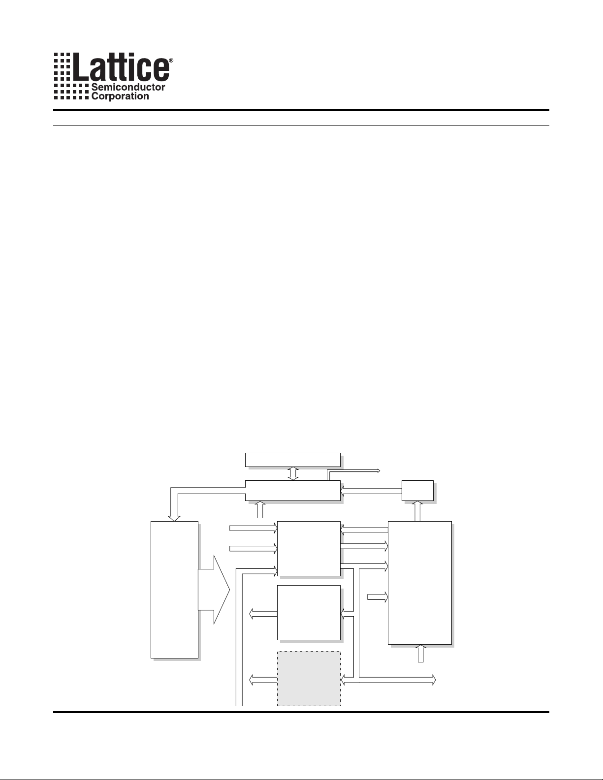
The following figure shows a block diagram of LatticeMico8 microcontroller.
Figure 1. LatticeMico8 Microcontroller Block Diagram
16 Deep Call Stack
Program Flow Control and PC
Interrupt
value
op A
op B
Immediate
value
Program
Memory
(EBR)
instr
17:0
rd
rb
From Mem
Register File
32 8-bit
Registers
Internal
32-byte Scratch
Pad Memory
Interrupt Ack
Flags
CY, Z
ALU
Optional External
Scratch Pad
(up to 256 Bytes)
From I/O Port
© 2006 Lattice Semiconductor Corp. All Lattice trademarks, registered trademarks, patents, and disclaimers are as listed at www.latticesemi.com/legal. All other brand
or product names are trademarks or registered trademarks of their respective holders. The specifications and information herein are subject to change without notice.
www.latticesemi.com
1
ALU Op
To I/O Port
rd1026_01.2
Page 2

LatticeMico8 Microcontroller
Lattice Semiconductor User’s Guide
Register File
The register file is implemented using dual ported distributed RAM. It contains 32 8-bit entries. Two values can be
simultaneously read from the register file.
Scratch Pad RAM (Internal)
The internal scratch pad memory has 32 entries. It can be addressed directly or indirectly (via a register). Indirect
addressing mode is not available if external scratch pad memory is attached.
Optional External Scratch Pad
The external scratch pad provides an additional 256 bytes of memory. It can be implemented using either distributed RAM or using an EBR. The external scratch pad memory can be addressed via indirect addressing only.
Hardware (Circular) Call Stack
When a call instruction is executed, the address of the next instruction is pushed into the call stack, a ret
(return) instruction will pop the stack and continue execution from the location at the top of the stack.
An interrupt also causes the address of the instruction that would have executed next to be pushed into the call
stack. The reti (return from interrupt) instruction will pop the stack and continue from the location at the top of the
stack.
The stack is implemented as a circular buffer and any program execution will continue from an undefined location in
case of a stack overflow or underflow.
Interrupt Handling
The microcontroller has one interrupt source, which is level sensitive. The interrupt can be enabled or disabled by
software ( cli = clear interrupt, sti = set interrupt). When an interrupt is received, the address of the next instruction is pushed into the call stack and the microcontroller continues execution from the interrupt vector (address 0).
The flags (carry and zero) are copied to shadow locations. The interrupt ack line is set high and the acknowledge line is held high for the entire duration of interrupt handling. Once the interrupt has been acknowledged the
interrupt line should be set to 0.
A reti instruction will pop the call stack and transfer control to the address on top of the stack. The Flags (carry
and zero) are restored from the shadow locations. The interrupt acknowledge line is set to low.
The microcontroller cannot handle nested interrupts.
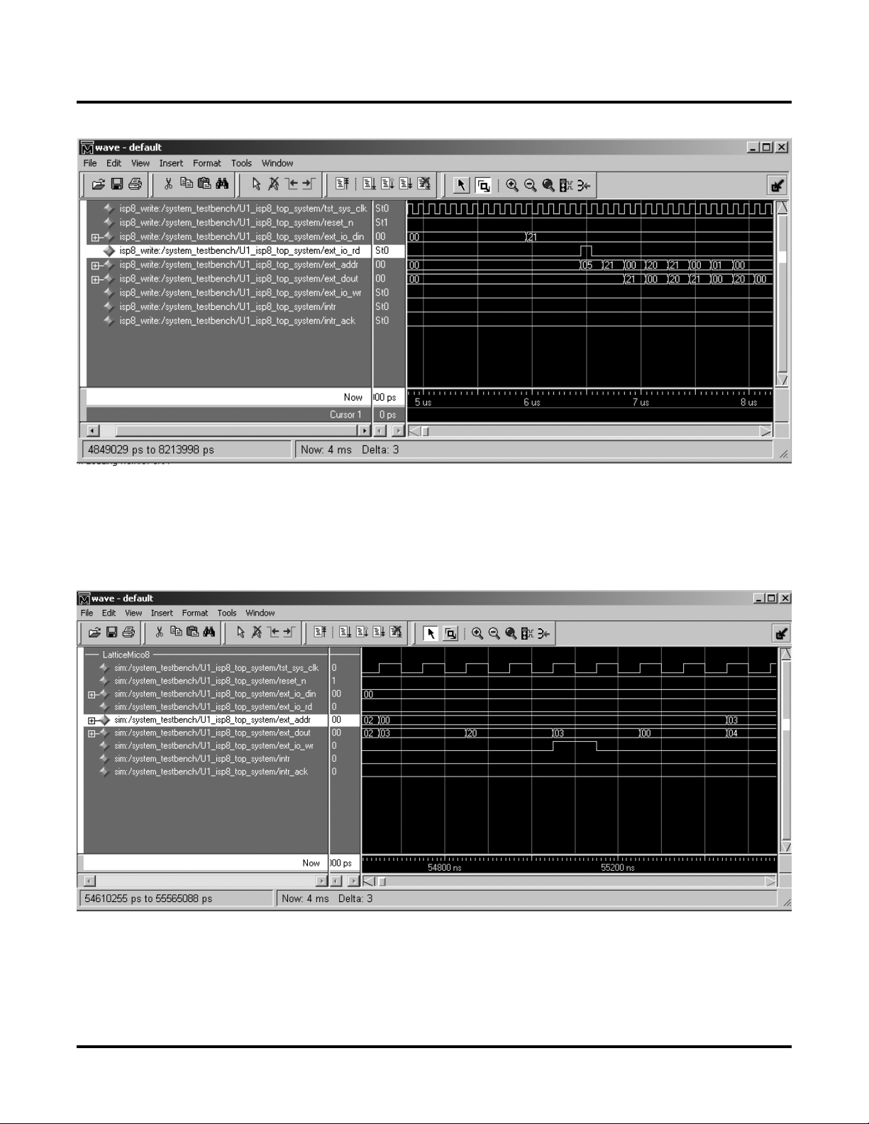
Input/Output
Input and output are done via “ports”. Up to 256 port numbers are allowed. The lower 32 ports can be addressed
directly (using the import and export instructions), or indirectly (using the importi and exporti instructions).
The upper 224 ports can be accessed by indirect addressing only (by the importi and exporti instructions).
The port number (0-31 of import , export and 0-255 for importi and exporti instructions) is presented at the
external interface for two cycles.
For import and importi instructions, the ext_io_rd signal is strobed in the same cycle as the input values are
sampled. The address signal is ext_addr and the input signals are ext_io_din . Both the address and the I/O
read strobe are driven in the second cycle. In the case of the importi instruction, the ext_addr signal is driven
from the register file; otherwise, for the import instruction, it is driven directly from the instruction. Figure 2 shows
the waveform corresponding to a read.
2
Page 3
LatticeMico8 Microcontroller
Lattice Semiconductor User’s Guide
Figure 2. Microcontroller Read Cycle Using import , importi
For export and exporti instructions, the ext_io_wr signal is strobed in the same cycle as the data out is
driven. Both the ext_io_wr and the ext_dout are driven in the second cycle of instruction execution. Figure 3
shows the waveform corresponding to a write. In the case of the exporti instruction, the ext_addr signal is
driven from the register file; otherwise, for the export instruction, it is driven directly from the instruction.
Figure 3. Microcontroller Write Cycle Using export , exporti
Scratch Pad Memory Access (External)
An optional scratch pad memory of up to 256 bytes can be attached externally to the processor. If external memory
is attached, the internal scratch pad can be accessed by direct addressing only ( LSP and SSP instructions). The
external memory can be accessed by indirect addressing only ( LSPI and SSPI instructions).
3
Page 4
LatticeMico8 Microcontroller
Lattice Semiconductor User’s Guide
Instruction Sets
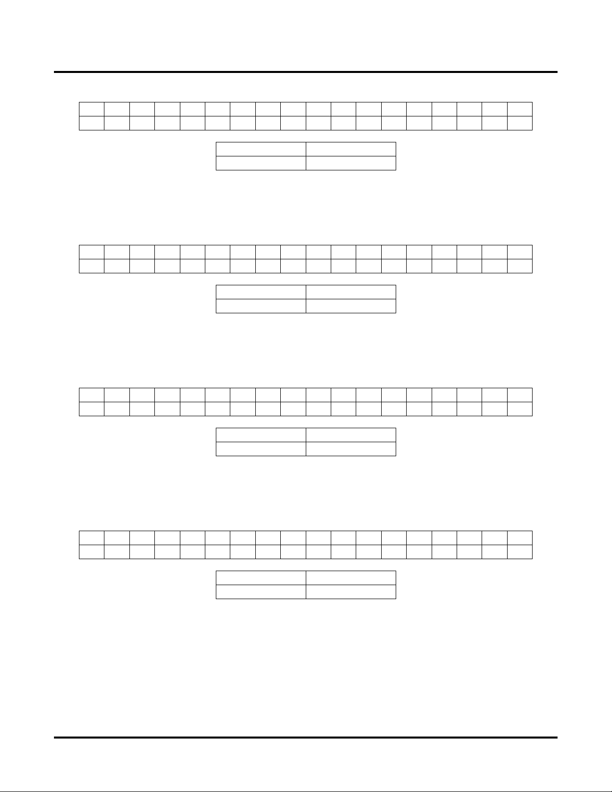
Please note that for all Branch and Call instructions, the signed offset is represented as binary 2’s complement.
ADD RD, Rb
17 16 15 14 13 12 11 10 9 8 76543210
0 1 0 0 Rd Rd Rd Rd Rd Rb Rb Rb Rb Rb 0 0 0
0
CY Flag Updated Zero Flag Updated
Ye s
Rd = Rd + Rb (add registers)
The carry flag is updated with the carry out from the addition. The zero flag is set to 1 if all the bits of the result are
0.
ADDI Rd, C
Ye s
17 16 15 14 13 12 11 10 9 8 76543210
0 1 0 1 Rd Rd Rd Rd Rd C C C C C C C C
0
CY Flag Updated Zero Flag Updated
Ye s
Ye s
Rd = Rd + CCCCCCCC (add constant to register)
The carry flag is updated with the carry out from the addition. The zero flag is set to 1 if all the bits of the result are
0.
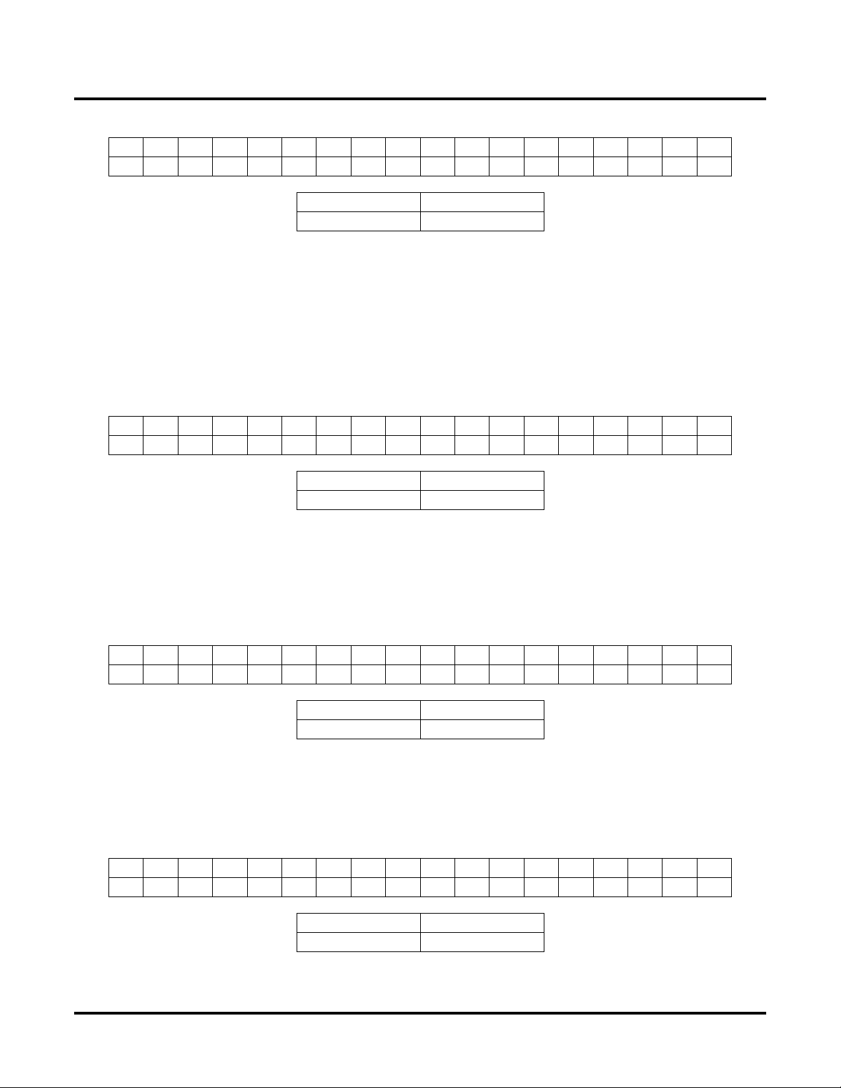
ADDC Rd, Rb
17 16 15 14 13 12 11 10 9 8 76543210
0
0 1 1 0 Rd Rd Rd Rd Rd Rb Rb Rb Rb Rb 0 0 0
CY Flag Updated Zero Flag Updated
Ye s
Ye s
Rd = Rd + Rb + Carry Flag (add registers and carry flag)
The carry flag is updated with the carry out from the addition. The zero flag is set to 1 if all the bits of the result are
0.
ADDIC Rd, CC
17 16 15 14 13 12 11 10 9 8 76543210
0
0 1 1 1 Rd Rd Rd Rd Rd C C C C C C C C
CY Flag Updated Zero Flag Updated
Ye s
Ye s
Rd = Rd + CCCCCCCC + Carry Flag (add register, constant and carry flag)
The carry flag is updated with the carry out from the addition. The zero flag is set to 1 if all the bits of the result are
0.
4
Page 5
LatticeMico8 Microcontroller
Lattice Semiconductor User’s Guide
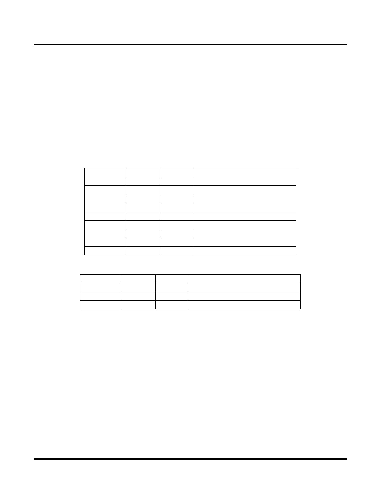
SUB Rd, Rb
17 16 15 14 13 12 11 10 9 8 76543210
00000RdRdRdRdRdRbRbRbRbRb000
CY Flag Updated Zero Flag Updated
Ye s Ye s
Rd = Rd - Rb (subtract register from register)
The carry flag is set to 1 if the result is negative. The zero flag is set to 1 if all the bits of the result are 0.
SUBI Rd, C
17 16 15 14 13 12 11 10 9 8 76543210
0
0 0 0 1 Rd Rd Rd Rd Rd C C C C C C C C
CY Flag Updated Zero Flag Updated
Ye s
Ye s
Rd = Rd - CCCCCCCC (subtract constant from register)
The carry flag is set to 1 if the result is negative. The zero flag is set to 1 if all the bits of the result are 0.
SUBC Rd, Rb
17 16 15 14 13 12 11 10 9 8 76543210
0
0 0 1 0 Rd Rd Rd Rd Rd Rb Rb Rb Rb Rb 0 0 0
CY Flag Updated Zero Flag Updated
Ye s
Ye s
Rd = Rd - Rb - Carry Flag (subtract register with carry from register)
The carry flag is set to 1 if the result is negative. The zero flag is set to 1 if all the bits of the result are 0.
SUBIC Rd, C
17 16 15 14 13 12 11 10 9 8 76543210
0 0 0 1 1 Rd Rd Rd Rd Rd C C C C C C C C
CY Flag Updated Zero Flag Updated
Ye s Ye s
Rd = Rd - CCCCCCCC - Carry Flag (subtract constant with carry from register)
The carry flag is set to 1 if the result is negative. The zero flag is set to 1 if all the bits of the result are 0.
5
Page 6

LatticeMico8 Microcontroller
Lattice Semiconductor User’s Guide
MOV Rd, Rb
17 16 15 14 13 12 11 10 9 8 76543210
0 1 0 0 0 Rd Rd Rd Rd Rd Rb Rb Rb Rb Rb 0 0 0
CY Flag Updated Zero Flag Updated
No Ye s
Rd = Rb (move register to register)
The zero flag is set to 1 if all the bits of the result are 0.
MOVI Rd, C
17 16 15 14 13 12 11 10 9 8 76543210
01001RdRdRdRdRdCCCCCCCC
CY Flag Updated Zero Flag Updated
No Yes
Rd = CCCCCCCC (move constant into register)
The zero flag is set to 1 if all the bits of the result are 0.
AND Rd, Rb
17 16 15 14 13 12 11 10 9 8 76543210
0 1 0 1 0 Rd Rd Rd Rd Rd Rb Rb Rb Rb Rb 0 0 0
CY Flag Updated Zero Flag Updated
No Ye s
Rd = Rd and Rb (bitwise AND registers)
The zero flag is set to 1 if all the bits of the result are 0.
ANDI Rd, C
17 16 15 14 13 12 11 10 9 8 76543210
0 1 0 1 1 Rd Rd Rd Rd Rd C C C C C C C C
CY Flag Updated Zero Flag Updated
No Ye s
Rd = Rd and CCCCCCCC (bitwise AND register with constant)
The zero flag is set to 1 if all the bits of the result are 0.
6
Page 7
LatticeMico8 Microcontroller
Lattice Semiconductor User’s Guide
OR Rd, Rb
17 16 15 14 13 12 11 10 9 8 76543210
0 1 1 0 0 Rd Rd Rd Rd Rd Rb Rb Rb Rb Rb 0 0 0
CY Flag Updated Zero Flag Updated
No Ye s
Rd = Rd | Rb (bitwise OR registers)
The zero flag is set to 1 if all the bits of the result are 0.
ORI Rd, C
17 16 15 14 13 12 11 10 9 8 76543210
0 1 1 0 1 Rd Rd Rd Rd Rd C C C C C C C C
CY Flag Updated Zero Flag Updated
No Ye s
Rd = Rd | CCCCCCCC (bitwise OR register with constant)
The zero flag is set to 1 if all the bits of the result are 0.
XOR Rd, Rb
17 16 15 14 13 12 11 10 9 8 76543210
0 1 1 1 0 Rd Rd Rd Rd Rd Rb Rb Rb Rb Rb 0 0 0
CY Flag Updated Zero Flag Updated
No Ye s
Rd = Rd and Rb (bitwise XOR registers)
The zero flag is set to 1 if all the bits of the result are 0.
XORI Rd, CC
17 16 15 14 13 12 11 10 9 8 76543210
0 1 1 1 1 Rd Rd Rd Rd Rd C C C C C C C C
CY Flag Updated Zero Flag Updated
No Ye s
Rd = Rd and CC (bitwise XOR register with constant)
The zero flag is set to 1 if all the bits of the result are 0.
7
Page 8

LatticeMico8 Microcontroller
Lattice Semiconductor User’s Guide
CMP Rd, Rb
17 16 15 14 13 12 11 10 9 8 76543210
1 0 0 0 0 Rd Rd Rd Rd Rd Rb Rb Rb Rb Rb 0 0 0
CY Flag Updated Zero Flag Updated
Ye s Ye s
Subtract Rb from Rd and update the flags. The result of the subtraction is not written back.
The carry flag is set to 1 if the result is negative. The zero flag is set to 1 if all the bits of the result are 0.
CMPI Rd, C
17 16 15 14 13 12 11 10 9 8 76543210
1 0 0 0 1 Rd Rd Rd Rd Rd C C C C C C C C
CY Flag Updated Zero Flag Updated
Ye s Ye s
Subtract Constant from Rd and update the flags. The result of the subtraction is not written back.
The carry flag is set to 1 if the result is negative. The zero flag is set to 1 if all the bits of the result are 0.
TEST Rd, Rb
17 16 15 14 13 12 11 10 9 8 76543210
1 0 0 1 0 Rd Rd Rd Rd Rd Rb Rb Rb Rb Rb 0 0 0
CY Flag Updated Zero Flag Updated
No Ye s
Perform a bitwise AND between Rd and Rb, update the zero flag. The result of the AND operation is not written
back.
The zero flag is set to 1 if all the bits of the result are 0.
TESTI Rd, CC
17 16 15 14 13 12 11 10 9 8 76543210
1 0 0 1 1 Rd Rd Rd Rd Rd C C C C C C C C
CY Flag Updated Zero Flag Updated
No Ye s
Perform a bitwise AND between Rd and Constant, update the zero flag. The result of the AND operation is not written back.
The zero flag is set to 1 if all the bits of the result are 0.
8
Page 9

LatticeMico8 Microcontroller
Lattice Semiconductor User’s Guide
ROR Rd, Rb
17 16 15 14 13 12 11 10 9 8 76543210
1 0 1 0 0 Rd Rd Rd Rd Rd Rb Rb Rb Rb Rb 0 0 0
CY Flag Updated Zero Flag Updated
No Ye s
MSB
Rotate right. Register B is shifted right one bit, the highest order bit is replaced with the lowest order bit. The result
is written back to Register Rd. The zero flag is set to 1 if all the bits of the result are 0.
RORC Rd, Rb
17 16 15 14 13 12 11 10 9 8 76543210
1 0 1 0 0 Rd Rd Rd Rd Rd Rb Rb Rb Rb Rb 0 0 1
CY Flag Updated Zero Flag Updated
Ye s Ye s
MSB
C
Rotate right through carry. The contents of Register B are shifted right one bit, the carry flag is shifted into the highest order bit, the lowest order bit is shifted into the carry flag. The zero flag is set to 1 if all the bits of the result are
0.
ROL Rd, Rb
17 16 15 14 13 12 11 10 9 8 76543210
1 0 1 0 0 Rd Rd Rd Rd Rd Rb Rb Rb Rb Rb 0 1 0
CY Flag Updated Zero Flag Updated
No Ye s
MSB
Rotate left. Register B is shifted left by one bit. The highest order bit is shifted into the lowest order bit. The zero flag
is set to 1 if all the bits of the result are 0.
9
Page 10

LatticeMico8 Microcontroller
Lattice Semiconductor User’s Guide
ROLC Rd, Rb
17 16 15 14 13 12 11 10 9 8 76543210
1 0 1 0 0 Rd Rd Rd Rd Rd Rb Rb Rb Rb Rb 0 1 1
CY Flag Updated Zero Flag Updated
Ye s Ye s
C
MSB
Rotate left through carry. Register B is shifted left by one bit. The carry flag is shifted into the lowest order bit and
the highest order bit is shifted into the carry flag. The zero flag is set to 1 if all the bits of the result are 0.
CLRC
17 16 15 14 13 12 11 10 9 8 76543210
1 0 1 1 0 0 0 0 0 0 0 0 0 0 0 0 0 0
Carry Flag = 0
Clear carry flag.
SETC
17 16 15 14 13 12 11 10 9 8 76543210
1 0 1 1 0 0 0 0 0 0 0 0 0 0 0 0 0 1
Carry Flag = 1
Set carry flag.
CLRZ
17 16 15 14 13 12 11 10 9 8 76543210
1 0 1 1 0 0 0 0 0 0 0 0 0 0 0 0 1 0
CY Flag Updated Zero Flag Updated
Ye s No
CY Flag Updated Zero Flag Updated
Ye s No
CY Flag Updated Zero Flag Updated
No Ye s
Zero Flag = 0
Clear zero flag.
10
Page 11

LatticeMico8 Microcontroller
Lattice Semiconductor User’s Guide
SETZ
17 16 15 14 13 12 11 10 9 8 76543210
1 0 1 1 0 0 0 0 0 0 0 0 0 0 0 0 1 1
CY Flag Updated Zero Flag Updated
No Ye s
Zero Flag = 1
Set zero flag.
CLRI
17 16 15 14 13 12 11 10 9 8 76543210
1 0 1 1 0 0 0 0 0 0 0 0 0 0 0 1 0 0
CY Flag Updated Zero Flag Updated
No No
Interrupt Enable Flag = 0
Clear interrupt enable flag. Disable interrupts.
SETI
17 16 15 14 13 12 11 10 9 8 76543210
1 0 1 1 0 0 0 0 0 0 0 0 0 0 0 1 0 1
CY Flag Updated Zero Flag Updated
No No
Interrupt Enable Flag = 1
Set interrupt enable flag. Enable interrupt.
BZ Label
17 16 15 14 13 12 11 10 9 8 76543210
1 1 0 0 1 0 0 0 L L L L L L L L L L
CY Flag Updated Zero Flag Updated
No No
If Zero Flag = 1 then PC = PC + (Signed Offset of Label). Else PC = PC + 1.
Branch if 0. If zero flag is set, the PC is incremented by the signed offset of the label from the current PC. If zero
flag is 0, then execution continues with the following instruction. The offset can be +/- 512.
11
Page 12

LatticeMico8 Microcontroller
Lattice Semiconductor User’s Guide
BNZ Label
17 16 15 14 13 12 11 10 9 8 76543210
1 1 0 0 1 0 0 1 L L L L L L L L L L
CY Flag Updated Zero Flag Updated
No No
If Zero Flag = 0 then PC = PC + (Signed Offset of Label). Else PC = PC + 1.
Branch if not 0. If zero flag is not set, the PC is incremented by the signed offset of the label from the current PC. If
zero flag is set, then execution continues with the following instruction. The offset can be +/- 512.
BC Label
17 16 15 14 13 12 11 10 9 8 76543210
1 1 0 0 1 0 1 0 L L L L L L L L L L
CY Flag Updated Zero Flag Updated
No No
If Carry Flag = 1 then PC = PC + (Signed Offset of Label). Else PC = PC + 1.
Branch if carry. If carry flag is set, the PC is incremented by the signed offset of the label from the current PC. If
carry flag is not set, then execution continues with the following instruction. The offset can be +/- 512.
BNC Label
17 16 15 14 13 12 11 10 9 8 76543210
1 1 0 0 1 0 1 1 L L L L L L L L L L
CY Flag Updated Zero Flag Updated
No No
If Carry Flag = 0 then PC = PC + (Signed Offset of Label). Else PC = PC + 1.
Branch if not carry. If carry flag is not set, the PC is incremented by the signed offset of the label from the current
PC. If carry flag is set, then execution continues with the following instruction. The offset can be +/- 512.
B Label
17 16 15 14 13 12 11 10 9 8 76543210
1 1 0 0 1 1 0 0 L L L L L L L L L L
CY Flag Updated Zero Flag Updated
No No
Unconditional Branch. PC = PC + Signed Offset of Label
Unconditional branch. PC is incremented by the signed offset of the label from the current PC. The offset can be +/-
512.
12
Page 13

LatticeMico8 Microcontroller
Lattice Semiconductor User’s Guide
CALLZ Label
17 16 15 14 13 12 11 10 9 8 76543210
1 1 0 1 1 0 0 0 L L L L L L L L L L
CY Flag Updated Zero Flag Updated
No No
If Zero Flag = 1, then
Push PC + 1 into Call Stack
PC = PC + Signed Offset of LABEL
Else, PC = PC + 1
CALL if 0. If the zero flag is set, the address of the next instruction (PC+1) is pushed into the call stack and the PC
is incremented by the signed offset of the label from the current PC. If zero flag is not set, then execution continues
from the following instruction.
CALLNZ Label
17 16 15 14 13 12 11 10 9 8 76543210
1 1 0 1 1 0 0 1 L L L L L L L L L L
CY Flag Updated Zero Flag Updated
No No
If Zero Flag = 0, then
Push PC + 1 into Call Stack
PC = PC + Signed Offset of LABEL.
Else PC = PC + 1
CALL if NOT 0. If the zero flag is not set, the address of the next instruction (PC+1) is pushed into the call stack,
and the PC is incremented by the signed offset of the label from the current PC. If the zero flag is set, then execution continues from the following instruction.
CALLC Label
17 16 15 14 13 12 11 10 9 8 76543210
1 1 0 1 1 0 1 0 L L L L L L L L L L
CY Flag Updated Zero Flag Updated
No No
If Carry Flag = 1, then
Push PC + 1 into Call Stack
PC = PC + Signed Offset of LABEL.
Else, PC = PC + 1
CALL if carry. If the carry flag is set, the address of the next instruction (PC+1) is pushed into the call stack, and the
PC is incremented by the signed offset of the label from the current PC. If the carry flag is not set, then execution
continues from the following instruction.
13
Page 14
LatticeMico8 Microcontroller
Lattice Semiconductor User’s Guide
CALLNC Label
17 16 15 14 13 12 11 10 9 8 76543210
1 1 0 1 1 0 1 1 L L L L L L L L L L
CY Flag Updated Zero Flag Updated
No No
If Carry Flag = 0, then
Push PC + 1 into Call Stack
PC = PC + Signed Offset of LABEL
Else, PC = PC + 1
CALL if not carry. If the carry flag is set, the address of the next instruction (PC+1) is pushed into the call stack, and
the PC is incremented by the signed offset of the label from the current PC. If the carry flag is not set, then execution continues from the following instruction.
CALL Label
17 16 15 14 13 12 11 10 9 8 76543210
1 1 0 1 1 1 0 0 L L L L L L L L L L
CY Flag Updated Zero Flag Updated
No No
Push PC + 1 into Call Stack
PC = PC + Signed offset of LABEL
Unconditional call. Address of the next instruction (PC+1) is pushed into the call stack, and the PC is incremented
by the signed offset of the label from the current PC.
RET
17 16 15 14 13 12 11 10 9 8 76543210
1 1 1 0 1 0 0 0 0 0 0 0 0 0 0 0 0 0
CY Flag Updated Zero Flag Updated
No No
PC = Top of Call Stack
Pop Call Stack
Unconditional return. PC is set to the value on the top of the call stack. The call stack is popped.
IRET
17 16 15 14 13 12 11 10 9 8 76543210
1 1 1 0 1 0 0 0 0 0 0 0 0 0 0 0 0 1
PC = Top of Call Stack
Pop Call Stack
CY Flag Updated Zero Flag Updated
No No
14
Page 15

LatticeMico8 Microcontroller
Lattice Semiconductor User’s Guide
Restore Zero and Carry Flags from shadow locations
Return from interrupt. In addition to popping the call stack, the carry and zero flags are restored from shadow locations.
IMPORT Rd, Port#
17 16 15 14 13 12 11 10 9 8 76543210
1 1 1 1 0 Rd Rd Rd Rd Rd P P P P P 0 0 1
CY Flag Updated Zero Flag Updated
No No
Rd = Value from Port (Port#)
Read value from port number (Port#) and write into register Rd. Port # can be 0-31.
IMPORTI Rd, Rb
17 16 15 14 13 12 11 10 9 8 76543210
1 1 1 1 0 Rd Rd Rd Rd Rd Rb Rb Rb Rb Rb 0 1 1
CY Flag Updated Zero Flag Updated
No No
Rd = Value from Port # in Register Rb
Indirect read of port. Value is read from port number in register Rb. Port number can be 0-255.
EXPORT Rd, Port#
17 16 15 14 13 12 11 10 9 8 76543210
1 1 1 1 0 Rd Rd Rd Rd Rd P P P P P 0 0 0
CY Flag Updated Zero Flag Updated
No No
Port Value(Port#) = Rd
Output value of Register D to Port#. Port# can be 0-31.
EXPORTI Rd, Rb
17 16 15 14 13 12 11 10 9 8 76543210
1 1 1 1 0 Rd Rd Rd Rd Rd Rb Rb Rb Rb Rb 0 1 0
CY Flag Updated Zero Flag Updated
No No
Port Value(Rb) = Rd
Output value of Register D to Port# designated by Register B. Port# can be 0-255.
15
Page 16

LatticeMico8 Microcontroller
Lattice Semiconductor User’s Guide
LSP Rd, SS
17 16 15 14 13 12 11 10 9 8 76543210
1 1 1 1 0 Rd Rd Rd Rd Rd S S S S S 1 0 1
CY Flag Updated Zero Flag Updated
No No
Rd = Scratch Pad(SS)
Load from scratch pad memory direct. Load the value from the scratch pad location designated by constant SS into
Register D. SS can be 0-31.
LSPI Rd, Rb
17 16 15 14 13 12 11 10 9 8 76543210
1 1 1 1 0 Rd Rd Rd Rd Rd Rb Rb Rb Rb Rb 1 1 1
CY Flag Updated Zero Flag Updated
No No
Rd = Scratch Pad (Rb)
Load from scratch pad memory indirect. Load the value from the scratch pad location designated by Register B into
Register D. The location address can be 0-255.
SSP Rd, SS
17 16 15 14 13 12 11 10 9 8 76543210
1 1 1 1 0 Rd Rd Rd Rd Rd S S S S S 1 0 0
CY Flag Updated Zero Flag Updated
No No
Scratch Pad (SS) = Rd
Store into scratch pad memory direct. Store value of register D into scratch pad memory location designated by
constant SS. The location address can be 0-31.
SSPI Rd, Rb
17 16 15 14 13 12 11 10 9 8 76543210
1 1 1 1 0 Rd Rd Rd Rd Rd Rb Rb Rb Rb Rb 1 1 0
CY Flag Updated Zero Flag Updated
No No
Scratch Pad (Rb) = Rd
Store into scratch pad memory indirect. Store value of register D, into scratch pad memory location designated by
register B. The location address can be 0-255.
16
Page 17
LatticeMico8 Microcontroller
Lattice Semiconductor User’s Guide
Configuration Options
The LatticeMico8 microcontroller has the following configurable features:
• Register File size: LatticeMico8 can be configured to have 16 or 32 registers. Default configuration is 32 8-bit
registers. Un-commenting the line `define REGISTERS_16, will configure the micro-controller with 16 registers.
Note: the Assembler will allow registers 16 through 31 to be used.
• Internal Scratch Pad memory size: Default configuration is 32 bytes. Un-commenting the `define
SCRATCH_PAD_MEM_16, will configure the controller to have 16 bytes of internal scratch pad memory.
• External memory interface: The external memory interface can be optionally enabled. This allows for adding an
extra 256 bytes of memory to the microcontroller. By default this is not available, un-commenting the line `define
EXT_SP_MEM will enable this feature.
I/O Configurations
Table 1. I/O with No External Scratch Pad Memory
Name In/Out Width (bits) Description
clk In 1 Clock
rst_n In 1 Reset active low
ext_io_din In 8 Input data for import
intr In 1 Interrupt active high
ext_addr Out 8 Address for import/export
ext_dout Out 8 Output data for export
ext_io_wr Out 1 High for export
ext_io_rd Out 1 High for import
intr_ack Out 1 Interrupt acknowledge active high
Table 2. I/O with 256 Bytes External Scratch Pad Memory
Name In/Out Width (bits) Description
ext_mem_din In 8 Input from external scratch pad
ext_mem_wr Out 1 High indicates write to external memory
ext_mem_rd Out 1 High indicates read from external memory
When `define EXT_SP_MEM is set, three extra ports are added to the controller to communicate with the external
scratch pad memory. The ext_dout is used to write data into the external memory. The address bus ext_addr is
also shared.
Assembler and Instruction Set Simulator
The software tools for the LatticeMico8 microcontroller include an Assembler and an Instruction Set Simulator, both
developed in C. The purpose of the Assembler is to generate an Embedded Block RAM (EBR) initialization file from
a text assembler input file. The purpose of the Simulator is to execute a program in the host environment. This section describes the use of these tools.
Assembler
The assembler reads in a text assembler source file (default extension .s) and creates one of the following as output:
• Hexadecimal output file (can be used by Module Manager)
• Binary output file (can be used by Module Manager)
17
Page 18

LatticeMico8 Microcontroller
Lattice Semiconductor User’s Guide
• Verilog initialization file (included in design before synthesis)
In addition to these outputs, the Assembler can also generate an assembler listing file.
Command Line
<executable filename> -option1 -option2 ... <input filename>
Command Line Options
Option Comment
-o <filename> Fully qualified name of the output file.
-s <Program Rom Size> Default 512 bytes
-l Generate listing file. The listing file is generated in the same directory as the
source with the extension .lst.
-vx Generate output in hexadecimal (default)
-vb Generate output in binary
-ve Generate output in Verilog “INIT” format
-? Help message
Instructions
The Assembler supports all instructions as described in the Instruction Set section.
Pseudo-Ops
The Assembler supports the following pseudo-ops:
Option Comment
nop Expanded by the Assembler to mov R0,R0. An instruction without side effects.
Labels
Label definitions are any character sequences ending in a ‘:’. No other instruction or Assembler directives are
allowed in the same line as a label definition.
The Assembler allows both forward and backward references to a label (i.e. it is legal to reference a label before it
is defined). Both references in the following example are valid.
BackLabel:
...
...
b BackLabel
...
...
b ForwardLabel
...
...
ForwardLabel:
Comments
The character ‘#’ is used as the start of a comment. Everything following the comment character until a new line is
ignored by the Assembler.
Constants
The assembler accepts constants in various formats.
• Hexadecimal values: Hexadecimal constants must be prefixed with “0x” or “0X”. (e.g. 0xFF, 0x12, and 0XAB are
all valid hexadecimal constants).
18
Page 19

LatticeMico8 Microcontroller
Lattice Semiconductor User’s Guide
• Octal values: Octal values must be prefixed with the numeric character ‘0’. (e.g. 077, 066, and 012 are valid
octal constants).
• Character constants: Single character constants must be enclosed in single quotation marks. (e.g. ‘A’, ‘v’, ‘9’
are all valid character constants).
• Decimal constants: Any sequence of decimal numbers can be a valid constant. (e.g. 123, 255, 231 are valid
decimal constants).
• Location counter: The special character $ (dollar sign) is used to give the current value of the location counter.
Note: The hexadecimal, octal, and decimal constants can be optionally prefixed with a ‘+’ or ‘-’ sign.
Assembler Directives
In addition to the instructions described in the Instruction Set section, the Assembler also supports the following
directives. An Assembler directive must be prefixed with a ‘.’ character.
• .org: This directive allows code to be placed at specific addresses. The syntax for this directive is:
.org <constant>
The constant can be of any form described in the previous section. The Assembler will terminate with an error, if
the .org directive is given a location which is less than the current “local counter” value.
• .equ: This directive can be used to assign symbolic names to constants. The syntax of the directive is:
.equ <symbolic name>,<constant>
.equ newline,’\n’
...
movi r2,newline
• .data: This directive can be used to embed arbitrary data in the assembler. The syntax for this directive is:
.data <constant>
The following figure is an example of the listing generated by the Assembler:
Figure 4. Example of Assembler Generated Listing
Loc Opcode Opcode
Counter (Hex) (Bin)
0x0000 0x33001 110011000000000001 b start
0x0001 start:
0x0001 0x10000 010000000000000000 nop
0x0002 add:
0x0002 0x12055 010010000001010101 movi R00,0x55
0x0003 0x12105 010010000100000101 movi R01,0x05
0x0004 0x12203 010010001000000011 movi R02,0x03
0x0005 0x08110 001000000100010000 add R01,R02
0x0006 0x0A101 001010000100000001 addi R01,0x01
0x0007 0x10308 010000001100001000 mov R03,R01
0x0008 0x10410 010000010000010000 mov R04,R02
0x0009 0x12535 010010010100110101 movi R05,0x35
0x000A 0x12643 010010011001000011 movi R06,0x43
0x000B 0x08628 001000011000101000 add R06,R05
0x000C 0x0A613 001010011000010011 addi R06,0x13
0x000D 0x10728 010000011100101000 mov R07,R05
•
•
•
19
Page 20

LatticeMico8 Microcontroller
Lattice Semiconductor User’s Guide
Building Assembler from Source
Although Lattice provides precompiled binary files, the source is available for compilation. The following commands
should be used in the Unix and Windows environments.
• Unix and Cygwin Environments:
gcc -o isp8asm isp8asm.c
• Windows Environment:
cl -o isp8asm_win isp8asm.c
Instruction Set Simulator
The software tools for LatticeMico8 include an Instruction Set Simulator for the microcontroller which allows programs developed for the microcontroller to be run and debugged on a host platform. The Simulator can also be
used to generate a disassembly listing of a LatticeMico8 program. The Simulator takes as input the memory output
file of the Assembler. It emulates the instruction execution of the LatticeMico8 in software. Please note that the
Simulator does not handle interrupts.
Command Line
<executable filename> -option1 -option2 ... <input filename>
Command Line Option
Option Comment
-p <Program Rom Size> Default is 512 bytes.
-x Use external scratch pad memory. Refer to the Functional Description section of
this document for details.
-ix Program file is in hexadecimal format (default). This is the file generated by the
Assembler with the -vx options (default).
-ib Program file is in binary format. This is the file generated by the Assembler with the
-vb option.
-t Trace the execution of the program. The Simulator will generate a trace as it executes each instruction. It will also print the modified value of any register (if the
instruction modifies a register value).
-d Generate a disassembly of the program specified by the PROM file.
Simulator Interactions
The import, importi and export, exporti instructions can be used to interact with the simulator. When an
export, exporti instruction is executed, the simulator will print the value of the port number as well as the con-
tents of the exported register. If the port number is 0xFF, the simulator will terminate with an exit code identical to
the value of the exported register. When an import, importi instruction is executed, the simulator will issue a
prompt containing the port number and read in values from the standard input (stdin). The following figure shows
an example of a traced simulation.
Figure 5. Example of Trace Simulation
0x00001 0x10000 mov R00,R00
0x00002 0x12055 movi R00,0x55
R00 = 0x55
0x00003 0x12105 movi R01,0x05
R01 = 0x05
0x00004 0x12203 movi R02,0x03
R02 = 0x03
0x00005 0x08110 add R01,R02
20
Page 21

LatticeMico8 Microcontroller
Lattice Semiconductor User’s Guide
R01 = 0x08
0x00006 0x0A101 addi R01,0x01
R01 = 0x09
0x00007 0x10308 mov R03,R01
R03 = 0x09
0x00008 0x10410 mov R04,R02
R04 = 0x03
0x00009 0x12535 movi R05,0x35
R05 = 0x35
0x0000A 0x12643 movi R06,0x43
R06 = 0x43
0x0000B 0x08628 add R06,R05
R06 = 0x78
0x0000C 0x0A613 addi R06,0x13
R06 = 0x8B
0x0000D 0x10728 mov R07,R05
R07 = 0x35
0x0000E 0x10830 mov R08,R06
R08 = 0x8B
0x0000F 0x12916 movi R09,0x16
R09 = 0x16
0x00010 0x12ADF movi R10,0xDF
R10 = 0xDF
•
•
•
Building Simulator from Source
Although Lattice provides precompiled binary files, the source is available for compilation. The following commands
should be used in the Unix and Windows environments.
• Unix and Cygwin Environments:
gcc -o isp8sim isp8sim.c
• Windows Environment:
cl -o isp8sim_win isp8sim.c
Example
To display the features and capabilities of the LatticeMico8, a demonstration example is also available. It demonstrates the interaction between the timer and the controller and the interrupt capability.
# This program will allow user to run a fibonacci number
# generator and updown counter. This program responds to
# the interrupt from the user (through Orcastra).
# When there is an interrupt, the program will halt the current program,
# and execute the int_handler function. When the intr_handler function
# is done, the program will continue from its last position
b int_handler
nop
nop
seti # set the program to be able to receive interrupt
nop
nop
b start
21
Page 22

LatticeMico8 Microcontroller
Lattice Semiconductor User’s Guide
start:
import r5, 5
mov r6, r5
andi r5, 0xf0 # masking r5 to decide type of program
mov r7, r5
mov r5, r6
andi r5, 0x0f # masking r5 to get the speed
mov r25, r5
cmpi r7, 0x10
bz phase2
cmpi r7, 0x20
bz phase2
b start
phase2:
cmpi r25, 0x01
bz phase3
cmpi r25, 0x02
bz phase3
cmpi r25, 0x03
bz phase3
cmpi r25, 0x04
bz phase3
b start
phase3:
cmpi r7, 0x10
bz fibo
cmpi r7, 0x20 # 1 = fibonacci, 2 = counter
bz counter
b start
22
Page 23

LatticeMico8 Microcontroller
Lattice Semiconductor User’s Guide
Implementation
Config.
Number Description
1 16 - Regs, 16 - Int SP, No Ext SP
2 32 - Regs, 16 - Int SP, No Ext SP
3 32 - Regs, 32 - Int SP, No Ext SP
4 32 - Regs, 32 - Int SP, Ext SP
1. SP = Scratch Pad
1
LFXP3C-4,
LFEC3E-4
LCMX01200C-4 214 71 109 78.6 (LCMXO1200C-4)
LFE2-50E-5 220 71 132 90.7 (LFE2-50E-5)
LFXP3C-4,
LFEC3E-4
LCMXO1200C-4 248 71 125 71.9 (LCMXO1200C-4
LFE2-50E-5 264 71 150 84.9 (LFE2-50E-5)
LFXP3C-4,
LFEC3E-4
LCMXO1200C-4 262 71 132 70.9 (LCMXO1200C-4)
LFE2-50E-5 295 71 172 84.3 (LFE2-50E-5)
LFXP3C-4,
LFEC3E-4
LCMXO1200C-4 73 141 141 70.8 (LCMXO1200C-4)
LFE2-50E-5 292 73 169 86.2 (LFE2-50E-5)
Technical Support Assistance
Hotline: 1-800-LATTICE (North America)
+1-503-268-8001 (Outside North America)
e-mail: techsupport@latticesemi.com
Internet: www.latticesemi.com
Device LUTs Registers SLICEs
198 71 114
247 71 138
243 71 136
275 73 151
(MHz)
f
MAX
71.4 (LFXP3C-4)
77.1 (LFEC3E-4)
62.4 (LFXP3C-4)
68.8 (LFEC3E-4)
63.4 (LFXP3C-4)
70.0 (LFEC3E-4)
62.3 (LFXP3C-4)
65.6 (LFEC3E-4)
23
 Loading...