

Page 1

LatticeECP2™ Standard Evaluation Board
User’s Guide
Revision: ebdug18_01.3
May 2007
Page 2
LatticeECP2 Standard Evaluation Board
Lattice Semiconductor User’s Guide
Introduction
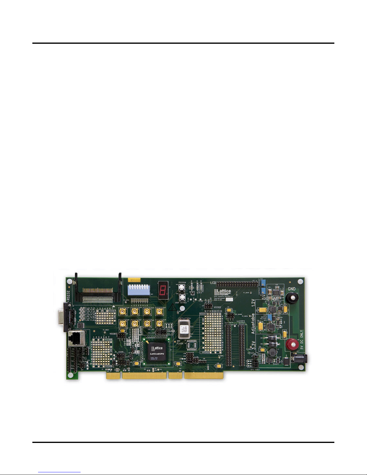
The LatticeECP2 Standard Evaluation Board is a complete, integrated design, featuring a LatticeECP2 FPGA and
a variety of both application-specific and general-purpose peripheral interfaces. This board provides a convenient
platform to evaluate, test, and debug user designs, including designs requiring PCI/PCI-X. This board includes the
following features:
• LatticeECP2 FPGA device in 484 fpBGA package
• SPI Serial Flash device included for low-cost, non-volatile configuration storage
• PCI/PCI-X edge connector (188-pin) supporting Master or Target
– PCI 2.2 - 32/64 bit, 33/66 MHz, 3.3V
– PCI-X - 32/64 bit, 66/133 MHz, parity or ECC, 3.3V (Mode 1)
• RS-232 connector
• 33.33 MHz oscillator
• RJ-45 connector
• LCD connector
• Compact Flash connector
• Prototyping area with access to over 210 I/O pins
• Optional SMA/SMB connectors (up to eight) for high-speed clock and data interfacing
• 7-segment display, eight general purpose switches, two momentary switches, eight user LEDs, and various sta-
tus LEDs
• Required voltages supplied by PCI/PCI-X or one external 5V DC supply
• ispVM
Figure 1. Lattice ECP2 Standard Evaluation Board
®
System programming support
Electrical, Mechanical, and Environmental Specifications
The nominal board dimensions are 9.75 inches by 4.2 inches. The environmental specifications are as follows:
• Operating temperature: 0ºC to 55ºC
• Storage temperature: -40ºC to 75ºC
2
Page 3
k
k
LatticeECP2 Standard Evaluation Board
Lattice Semiconductor User’s Guide
• Humidity: < 95% without condensation
• 5VDC input (+/- 10%) up to 4A, or 3.3V input from PCI/PCI-X backplane
Additional Resources
Additional resources relating to the LatticeECP2 Standard Evaluation Board (including updated documentation,
and sample programs) can be found at the following URL:
www.latticesemi.com/products/developmenthardware/fpgafspcboards/ecp2stardevaluationboard.cfm
Features
LatticeECP2 Device
This board features a LatticeECP2 FPGA with a 1.2V DC core in a 484-ball fpBGA package. A complete description of this device can be found in the LatticeECP2 Family Data Sheet available on the Lattice web site at www.latticesemi.com/ecp2.
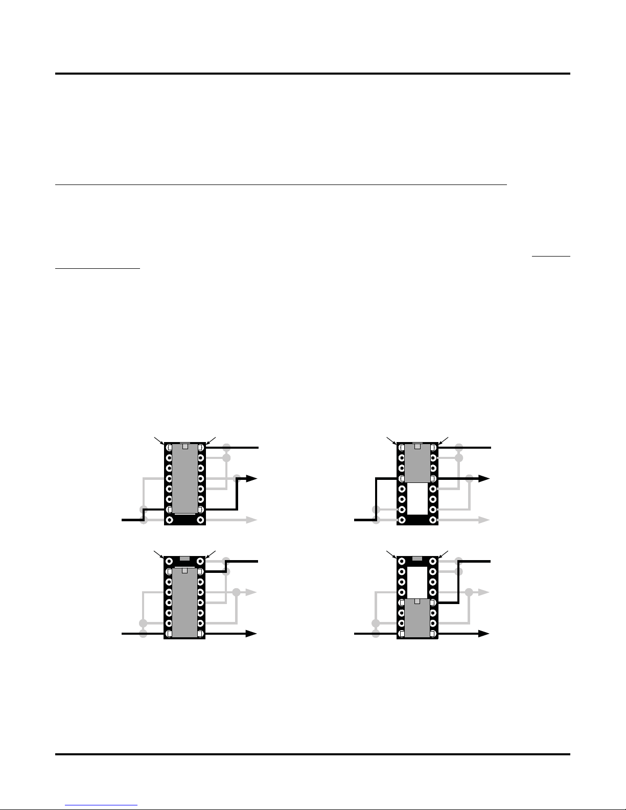
On-Board Oscillator
The 3.3V oscillator socket at Y1 accepts both full-size (14-pin) and half-size (8-pin) oscillators, and will route the
oscillator output to a LatticeECP2 primary clock input or a PLL input, depending on the oscillator’s position in the
socket (see Figure 2).
When a full size oscillator is installed such that pin 1 of the oscillator aligns with pin 1 of the socket, the output of
the oscillator drives the primary clock at LatticeECP2 pin J21 (this is the default position). When pin 1 of the oscillator is aligned to pin 2 of the socket, the clock is routed to LatticeECP2 pin J21. When using a half size oscillator,
align pin 1 of the oscillator to pin 1 of the socket to drive the primary clock, or align pin 1 of the oscillator to pin 5 of
the socket to drive the PLL. Note that pin 1 of the oscillator is expected to be a no-connect pin.
Figure 2. Oscillator Options
GND
GND
Pin-1 Pin-1
Default
Position
Pin-1
33.33 MHz
Full-Size
33.33 MHz
Full-Size
Pin-16 Pin-16
3.3V
Primary Clock
(J21)
PLL Clock
(N21)
3.3V
Primary Clock
(J21)
PLL Clock
(N21)
GND
Pin-1Pin-16
GND
33.33 MHz
Half-Size
33.33 MHz
Half-Size
Pin-16
3.3V
Primary Cloc
(J21)
PLL Clock
(N21)
3.3V
Primary Cloc
(J21)
PLL Clock
(N21)
SPI Serial Flash
SPI Serial Flash are available in three package styles, two of those packages, 8-pin SO and 16-pin SO, are supported by this board. In general, the 8-pin devices support densities up to 16Mb, while the 16-pin devices support
larger densities. The device chosen for inclusion on this board depends on the density of the installed LatticeECP2,
but the SPI Serial Flash will be large enough to allow two bitstreams to be stored simultaneously in order to support
SPIm mode.
3
Page 4
LatticeECP2 Standard Evaluation Board
Lattice Semiconductor User’s Guide
The 8-pin device footprint is at U4; the 16-pin device footprint is at U5. Only one location can be populated at a
time.
Configuration/Programming Headers
Two programming headers are provided on the evaluation board, providing access to the LatticeECP2 JTAG port
and sysCONFIG™ port. The JTAG connector is a 1x10 header and the sysCONFIG connector is a 2x17 header.
Both the JTAG and the sysCONFIG ports are also provided with loop-through connectors to allow for easy daisy
chaining of multiple boards. With proper jumper selection (see the next section) standard IDC ribbon cable can be
used without the need to swap wires on the cable.
See the Configuring/Programming The Board section of this document for more information on this topic.
The pinouts for these headers are provided in the following tables.
Note: A parallel port ispDOWNLOAD
using a parallel port (1x8) ispDOWNLOAD cable, connect pin 1 of the cable to pin 1 of the 1x10 JTAG header. For
more information on the ispDOWNLOAD Cable, see the ispDOWNLOAD Cables Data Sheet available on the Lattice web site at www.latticesemi.com.
®
cable is included with each LatticeECP2 Standard Evaluation Board. When
Table 1. JTAG Programming Header Pinout
Function
Vcc (3.3V)
1
TDO
TDI 3
PROGN
1
N/C 5
TMS 6
Ground 7
1
TCK
DONE 9
INIT Chain
1. See section below on jumpers.
Table 2. JTAG Loop-Through Header Pinout
Function
N/C
TDO Chain
TDI Chain
PROGN
N/C 5
TMS 6
Ground 7
TCK
DONE 9
INIT Chain
1. See section below on jumpers.
1
1
J4 (1x10)
1
2
4
8
1
10
J5 (1x10)
1
1
1
2
3
4
8
1
10
4
Page 5
LatticeECP2 Standard Evaluation Board
Lattice Semiconductor User’s Guide
Table 3. sysCONFIG Header Pinout (J40)
Function Pin Function
CCLK
BUSY / SISPI
1
DI/D0
D7 / DOUT
DONE
D7
D6
D5
D4
D3
D2
D1
D0
CSN
CS1N
Vcc Bank8
Ground
1. See section below on jumpers.
1
11 12
13 14
15 16
17 18
19 20
21 22
23 24
25 26
1
1
27 28
29 30
31 32
33 34
1 2
3 4
5 6
7 8
9 10
Ground
D6
Vcc Bank8
INITN
PROGRAMN
Ground
Ground
Ground
Ground
Ground
Ground
Ground
Ground
WRITEN
CFG0
CFG1
CFG2
Table 4. sysCONFIG Loop-Through Header Pinout (J41)
Function Pin Function
CCLK
N/C 3 4 N/C
DOUT / CSSON 5 6 N/C
N/C 7 8 INITN
DONE 9 10 PROGRAMN
D7 11 12 Ground
D6 13 14 Ground
D5 15 16 Ground
D4 17 18 Ground
D3 19 20 Ground
D2 21 22 Ground
D1 23 24 Ground
D0 25 26 Ground
CSN / N/C
CS1N / N/C
N/C 31 32 N/C
Ground 33 34 N/C
1. See section below on jumpers.
1
1
1 2 Ground
27
29
28 WRITEN
30 N/C
JTAG and sysCONFIG Jumpers
There are several JTAG and sysCONFIG cabling options that can be selected using jumpers.
5
Page 6
J8
LatticeECP2 Standard Evaluation Board
Lattice Semiconductor User’s Guide
Default Jumpers Settings
This table lists the default settings for all of the jumpers on the LatticeECP2 Standard Evaluation Board. For a complete description of each jumper refer to the next sections.
Table 5. Default Jumper Settings
JTAG Jumpers
Table 6. TDO Chain Jumper
Location
J1
J3 1 to 2 J30
J7 2 to 3 J31 Open
J8 1 to 2 J32 Open
J9 Open J33 1 to 2
J10 Open J34 2 to 3
J11 Open J35 Open
J13 Open J36 Open
J17 1 to 2 J37 1 to 2
J18 1 to 2 J38 Open
J19 Open J39 1 to 2
J22 Open J43
J23 Open J44 1 to 2
J24 Open
Position Location Position
1 to 2 J29 1 to 2
1 to 2
3 to 4
5 to 6
1 to 2
3 to 4
5 to 6
Location
J7
Determines the JTAG TDO path.
Position Function Default
1 to 2 Multiple boards, but not the last board in the chain
2 to 3
Single board, or the last board in a chain X
Table 7. TCK Pull-Down
Location
There should be only one TCK pull-down on a JTAG chain.
Position Function Default
1 to 2
Open
Pull-down, 4.7K to ground X
No pull-down
Table 8. PROGRAMN Pin to JTAG
Location
J10
This jumper is normally not installed.
Position Function Default
1 to 2 Connects PROGRAMN pin to the JTAG chain
Open
Disconnects PROGRAMN pin from JTAG chain X
6
Page 7
LatticeECP2 Standard Evaluation Board
Lattice Semiconductor User’s Guide
Table 9. INITN Pin to JTAG
Location
J11
This jumper is normally not installed.
Position Function Default
1 to 2 Connects INITN pin to the JTAG chain
Open
Disconnects INITN pin from the JTAG chain X
sysCONFIG Jumpers
Table 10. CS1N
Location
J31
Position Function Default
1 to 2 Pulls CS1N high
2 to 3 Pulls CS1N low
Open
No pull-up or pull-down on CS1N X
Table 11. CSN
Location Position Function Default
1 to 2 Pulls CSN high
J32
2 to 3 Pulls CSN low
Open
No pull-up or pull-down on CSN X
Table 12. DI/D[0]
Location Position Function Default
J33
1 to 2
2 to 3 Routes data bit D[0] to J40-5 for SPIFAST support
Routes DI to J40-5 to support serial mode X
Table 13. D[7]/DOUT
Location Position Function Default
J34
1 to 2 Routes D[7] to J40-7 for SPI sysCONFIG support
2 to 3
Routes DOUT to J40-7 to support serial mode X
Table 14. CSON to CS1N (Loop-Through)
Location Position Function Default
J35
1 to 2 CSON drives CS1N on the loop-through connector
Open
CS1N on the loop-through connector is open X
Table 15. CSON to CSN (Loop-Through)
Location Position Function Default
J36
1 to 2 CSON drives CSN on the loop-through connector
Open
CSN on the loop-through connector is open X
7
Page 8
LatticeECP2 Standard Evaluation Board
Lattice Semiconductor User’s Guide
Table 16. Configuration Mode (J43)
Configuration
Mode
SPI (default)
Reserved Jumper (0) Jumper (0) Open (1)
SPIm Jumper (0) Open (1) Jumper (0)
Reserved Jumper (0) Open (1) Open (1)
Reserved Open (1) Jumper (0) Jumper (0)
Slave Serial Open (1) Jumper (0) Open (1)
Reserved Open (1) Open (1) Jumper (0)
Slave Parallel Open (1) Open (1) Open (1)
CFG[2],
1 to 2
Jumper (0) Jumper (0) Jumper (0)
CFG[1],
3 to 4
CFG[0],
5 to 6
Table 17. SPIFAST
Location
J44
All SPI Serial Flash shipped with this board support fast read. This jumper must be removed when using the sysCONFIG parallel port.
Position Function Default
1 to 2
Open
SPI fast read, enables read op-code 0x0B X
SPI normal read, enables read op-code 0x03
Table 18. Jumper Settings for sysCONFIG Parallel
Location
J31
J32 Open See schematic
J33 1 to 2
J34 2 to 3
J43 All Open
J44 Open
J35, J36 Open Bypass Overflow
J35, J36 1 to 2 Flow-through Overflow
Position Notes
Open See schematic
Table 19. Jumper Settings for sysCONFIG Serial
Location
J31
J32 Open
J33 1 to 2
J34 2 to 3
J43
J44 Don’t Care
J35, J36 Open Bypass Overflow
J35, J36 1 to 2 Not allowed
Position Notes
Open
Open
3 to 4 Open if driven by cable
Open
8
Page 9
LatticeECP2 Standard Evaluation Board
Lattice Semiconductor User’s Guide
Table 20. Jumper Settings for SPI Emulation via J40
Location
J31
J32 Open
J33 2 to 3
J34 1 to 2
J43
J44 Open
J35, J36 Open Bypass Overflow
J35, J36 1 to 2 Not allowed
Position Notes
Open
1 to 2 Open if driven by cable
3 to 4 Open if driven by cable
5 to 6 Open if driven by cable
Power Setup
For stand-alone board operation, i.e. outside of a PCI/PCI-X backplane, the evaluation board must be supplied with
a single 5V DC power supply. 5V DC power may be applied using an AC adapter, such as the Condor Electronics
S-5V0-4A0-U11-206IP (or similar), plugged into the power jack at J47, or via the banana jacks at J45 (ground) and
J46 (5V DC).
Table 21. AC Adaptor Specifications
Voltage 5VDC +/- 10%
Current Capacity Up to 4A
Polarity Positive Center
Connector I.D. 0.1” (2.5mm)
Connector O.D. 0.218” (5.5mm)
When the board is inserted into a PCI/PCI-X backplane, the on-board 3.3V regulator is automatically disabled; all
onboard power will be derived from the PCI/PCI-X 3.3V power rail.
Additional on-board regulators supply 1.2V, an adjustable voltage, and 5V (for the optional LCD panel). The adjustable voltage is set by the potentiometer R36, on the right side of the board, and can be set to any value between
1.22V and 2.5V.
The header at J30 allows a current measuring device to be inserted between 1.2V and the FPGA core. To measure
current remove power from the board, remove all of the jumpers at J30, install a meter between the odd pins and
the even pins, for example between pins 1 and 2, and apply power to the board. When measurement is complete,
remove power from the board and re-install all three jumpers.
Table 22. 1.2V to V
Location
J30
The header at J29 allows a current measuring device to be inserted between 3.3V and the FPGA’s V
Core
CC
Position Function Default
1 to 2
3 to 4 X
5 to 6 X
Connects 1.2V to the FPGA Core
X
CCAUX.
To
measure current, remove power from the board, remove the jumper at J29, install a meter between pins 1 and 2,
and apply power to the board. When measurement is complete, remove power from the board and re-install the
jumper.
9
Page 10
LatticeECP2 Standard Evaluation Board
Lattice Semiconductor User’s Guide
Table 23. 3.3V to V
Location
J29
CCAUX
Position Function Default
1 to 2 Connects 3.3V to VCCAUX X
The LatticeECP2 is divided into 10 banks of I/Os (see Table 24), and each of these banks has a separate and independent V
Each bank supports voltages from 1.2V to 3.3V. However, because some banks, such as banks 4
CC.
and 5, which connect to PCI/PCI-X, require a fixed voltage, not all of the banks on this evaluation board are adjustable. The jumpers listed in Table 24 allow the user to select the voltage (V
) applied to the adjustable banks.
CCIO
Note that if the LatticeECP2 will be configured from the SPI Serial Flash, bank 8 must be set to 3.3V (because SPI
Serial Flash is 3.3V). Also, if the board is plugged into a PCI/PCI-X connector, bank 6 must be set to 3.3V (because
the PCI clock is routed to bank 6 on this board).
Table 24. Bank Voltage Selection
Bank
0 I/O — 3.3V Only
1 I/O — 3.3V Only
2 I/O J37
3 I/O — 3.3V Only
4 I/O — 3.3V Only
5 I/O — 3.3V Only
6 I/O J18
7 I/O J17
8 sysCONFIG J39
V
CCJ
J17, 18, 37, and 39 must have no more than one jumper installed.
Function Jumper Settings
1 - 2 = 3.3V
3 - 4 = ADJ
5 - 6 = 1.2V
1 - 2 = 3.3V
3 - 4 = ADJ
5 - 6 = 1.2V
1 - 2 = 3.3V
3 - 4 = ADJ
5 - 6 = 1.2V
1 - 2 = 3.3V
3 - 4 = ADJ
5 - 6 = 1.2V
ispJTAG™
— 3.3V Only
The following tables detail the various I/O standards supported by the LatticeECP2 sysIO™ structures. More information can be found in Lattice technical note TN1102, LatticeECP2 sysIO Usage Guide, available on the Lattice
web site at www.latticesemi.com.
Table 25. Mixed Voltage I/O Support
Input sysIO Standards
V
CCIO
1.2V
1.5V Ye s Ye s Ye s Ye s Ye s
1.8V Ye s Ye s Ye s Ye s Ye s
2.5V Ye s Ye s Ye s Ye s
3.3V Ye s Ye s Ye s Ye s
For example, if V
1.2V 1.5V 1.8V 2.5V 3.3V 1.2V 1.5V 1.8V 2.5V 3.3V
Ye s Ye s Ye s Ye s
is 3.3V, then signals from devices powered by 1.2V, 2.5V, or 3.3V can be input and the
CCIO
thresholds will be correct, assuming the user has also selected the desired input level using ispLEVER
Output levels are tied directly to V
CCIO.
10
Output sysIO Standards
®
software.
Page 11
LatticeECP2 Standard Evaluation Board
Lattice Semiconductor User’s Guide
Table 26. sysIO Standards Supported per Bank
Top Side,
Description
Types of I/O Buffers
Output Standards
Supported
Banks 0-1
Single-ended Single-ended and
LVTTL
LVCMOS33
LVCMOS25
LVCMOS18
LVCMOS15
LVCMOS12
SSTL18 Class I, II
SSTL25 Class I, II
SSTL33 Class I, II
HSTL15 Class I
HSTL18_I, II
SSTL18D Class I, II
SSTL25D Class I, II
SSTL33D Class I, II
HSTL15D Class I
HSTL18D Class I, II
PCI33
LVDS25E
LVPECL
BLVDS
RSDS
1
1
1
1
Inputs All Single-ended, Differ-
ential
Clock Inputs All Single-ended, Differ-
ential
Right Side,
Banks 2-3
Differential
LVTTL
LVCMOS33
LVCMOS25
LVCMOS18
LVCMOS15
LVCMOS12
SSTL18 Class I, II
SSTL25 Class I, II
SSTL33 Class I, II
HSTL15 Class I
HSTL18 Class I, II
SSTL18D Class I, II
SSTL25D Class I, II
SSTL33D Class I, II
HSTL15D Class I, II
HSTL18D Class I, II
PCI33
LVDS
LVDS25E
LVPECL
BLVDS
RSDS
1
1
1
1
All Single-ended,
Differential
All Single-ended,
Differential
Bottom Side,
Banks 4-5
Left Side,
Banks 6-7
Single-ended Single-ended and
Differential
LVTTL
LVCMOS33
LVCMOS25
LVCMOS18
LVCMOS15
LVCMOS12
SSTL18 Class I
SSTL2 Class I, II
SSTL3 Class I, II
HSTL15 Class I
HSTL18 Class I, II
SSTL18D Class I, II
SSTL25D Class I, II,
SSTL33D Class I, II
HSTL15D Class I
HSTL18D Class I, II
PCI33
LVDS25E
LVPECL
BLVDS
RSDS
1
1
1
1
All Single-ended,
Differential
All Single-ended,
Differential
LVTTL
LVCMOS33
LVCMOS25
LVCMOS18
LVCMOS15
LVCMOS12
SSTL18 Class I
SSTL2 Class I, II
SSTL3 Class I, II
HSTL15 Class I, III
HSTL18 Class I, II, III
SSTL18D Class I,
SSTL25D Class I, II,
SSTL33D_I, II
HSTL15D Class I
HSTL18D Class I, II
PCI33
LVDS
LVDS25E
LVPECL
BLVDS
RSDS
1
1
1
1
All Single-ended,
Differential
All Single-ended,
Differential
PCI Support PCI33 no clamp PCI33 no clamp PCI33 with clamp PCI33 no clamp
LVDS Output Buffers LVDS (3.5mA) Buffers
1. These differential standards are implemented by using complementary LVCMOS drivers and external resistors.
2. Available on 50% of the I/Os in the Bank.
2
LVDS (3.5mA) Buffers
2
PCI/PCI-X
The LatticeECP2 Standard Evaluation Board is designed to be compatible with PCI (PCI SIG 2.2 specification) and
PCI-X (Mode 1). All necessary signals required for 64-bit PCI/PCI-X operation are provided, as shown in Table 27
and Table 28.
Table 27. PCI Connections - Solder Side
J48 Signal Name LatticeECP2 Pin sysIO Bank Note
1 PCI_TRSTN - - TP10, PD if master
2 +12V - - Decoupling cap
3 PCI_TMS - - TP11, PU if master
4 PCI_TDI - - TP12, J14-4, J13
5 +5V - - NC
6 PCI_INTA_N - - J19
7 PCI_INTC_N - - J19
11
Page 12

LatticeECP2 Standard Evaluation Board
Lattice Semiconductor User’s Guide
Table 27. PCI Connections - Solder Side (Continued)
J48 Signal Name LatticeECP2 Pin sysIO Bank Note
8 +5V - - NC
9 PCIX_ECC5 W4 5
10 +3.3V - -
11 PCIX_ECC3 W5 5
14 +3.3VAUX - - TP13
15 PCI_RST_N Y4 5
16 +3.3V - -
17 PCI_GNT_N Y5 5
18 GND - -
19 PME# - - TP9
20 PCI_AD30 W6 5
21 3.3V - -
22 PCI_AD28 Y6 5
23 PCI_AD26 W7 5
24 GND - -
25 PCI_AD24 Y7 5
26 PCI_IDSEL U9 5
27 +3.3V - -
28 PCI_AD22 W8 5
29 PCI_AD20 Y8 5
30 GND
31 PCI_AD18 V9 5
32 PCI_AD16 W9 5
33 +3.3V - -
34 PCI_FRAME_N U10 5
35 GND - -
36 PCI_TRDY_N V10 5
37 GND - -
38 PCI_STOP_N W10 5
39 +3.3V - -
40 PCI_SMBCLK - - TP8, PU if master
41 PCI_SMBDAT - - TP14, PU if master
42 GND - -
43 PCI_PAR Y10 5
44 PCI_AD15 W11 5
45 +3.3V - -
46 PCI_AD13 U12 4
47 PCI_AD11 Y12 4
48 GND - -
49 PCI_AD9 W12 4
52 PCI_CBE0_N V12 4
53 +3.3V - -
54 PCI_AD6 U13 4
55 PCI_AD4 Y13 4
12
Page 13

LatticeECP2 Standard Evaluation Board
Lattice Semiconductor User’s Guide
Table 27. PCI Connections - Solder Side (Continued)
J48 Signal Name LatticeECP2 Pin sysIO Bank Note
56 GND - -
57 PCI_AD2 W13 4
58 PCI_AD0 U14 4
59 +3.3V - -
60 PCI_REQ64_N W14 4
61 NC - -
62 NC - -
63 GND - -
64 PCI_CBE7_N V14 4
65 PCI_CBE5_N U15 4
66 +3.3V - -
67 PAR64 T15 4
68 PCI_AD62 Y15 4
69 GND - -
70 PCI_AD60 W15 4
71 PCI_AD58 U16 4
72 GND - -
73 PCI_AD56 V16 4
74 PCI_AD54 T16 4
75 +3.3V - -
76 PCI_AD52 Y16 4
77 PCI_AD50 W16 4
78 GND - -
79 PCI_AD48 Y17 4
80 PCI_AD46 W17 4
81 GND - -
82 PCI_AD44 Y18 4
83 PCI_AD42 W18 4
84 +3.3V - -
85 PCI_AD40 Y19 4
86 PCI_AD38 Y20 4
87 GND - -
88 PCI_AD36 V17 4
89 PCI_AD34 V18 4
90 GND - -
91 PCI_AD32 U18 4
92 NC - -
93 GND - -
94 NC - -
Note: PD = pull-down resistor, PU = pull-up resistor, NC = no-connect, TP = test point.
13
Page 14

LatticeECP2 Standard Evaluation Board
Lattice Semiconductor User’s Guide
Table 28. PCI Connections - Component Side
J14 Signal Name LatticeECP2 Pin sysIO Bank Notes
1 -12V - - Decoupling cap
2 PCI_TCK - - TP16, PD if master
3 GND - -
4 PCI_TDO - - TP17, J3, J13
5 +5V - - NC
6 +5V - - NC
7 PCI_INTB_N - - J19
8 PCI_INTD_N - - J19
9 PCI_PRSNT1_N J14 -
10 PCIX_ECC4 W3 5
11 PCI_PRSNT2_N - - J23
14 PCIX_ECC2 Y2 5
15 GND - -
16 PCI_CLK R1 6 D20, J22
17 GND - -
18 PCI_REQ_N Y3 5
19 +3.3V - -
20 PCI_AD31 AB2 5
21 PCI_AD29 AA3 5
22 GND - -
23 PCI_AD27 AB3 5
24 PCI_AD25 AB4 5
25 3.3V - -
26 PCI_CBE3_N AA5 5
27 PCI_AD23 AB5 5
28 GND - -
29 PCI_AD21 AA6 5
30 PCI_AD19 AB6 5
31 3.3V - -
32 PCI_AD17 AB7 5
33 PCI_CBE2_N AA7 5
34 GND - -
35 PCI_IRDY_N AB8 5
36 +3.3V - -
37 PCI_DEVSEL_N U11 5
38 PCIXCAP - -
39 LOCK# - - TP15
40 PCI_PERR_N AA8 5
41 +3.3V - -
42 PCI_SERR_N AA9 5
43 +3.3V - -
44 PCI_CBE1_N AB9 5
45 PCI_AD14 AA10 5
46 GND - -
14
Page 15
LatticeECP2 Standard Evaluation Board
Lattice Semiconductor User’s Guide
Table 28. PCI Connections - Component Side (Continued)
J14 Signal Name LatticeECP2 Pin sysIO Bank Notes
47 PCI_AD12 AB10 5
48 PCI_AD10 AA11 5
49 PCI_M66EN - - J38
52 PCI_AD8 AB11 5
53 PCI_AD7 Y11 5
54 +3.3V - -
55 PCI_AD5 AB12 5
56 PCI_AD3 AA12 5
57 PCI_GND_57 - - U6
58 PCI_AD1 AB13 5
59 +3.3V - -
60 PCI_ACK64_N AA13 4
61 +5V - - NC
62 +5V - - NC
63 NC - -
64 GND - -
65 PCI_CBE6_N AB14 5
66 PCI_CBE4_N AA14 4
67 GND - -
68 PCI_AD63 AB15 4
69 PCI_AD61 AA15 4
70 +3.3V - -
71 PCI_AD59 AB16 4
72 PCI_AD57 AA16 4
73 GND - -
74 PCI_AD55 AB17 4
75 PCI_AD53 AA17 4
76 GND - -
77 PCI_AD51 AB18 4
78 PCI_AD49 AA18 4
79 +3.3V - -
80 PCI_AD47 AB19 4
81 PCI_AD45 AB20 4
82 GND - -
83 PCI_AD43 AA20 4
84 PCI_AD41 AB21 4
85 GND - -
86 PCI_AD39 AA22 4
87 PCI_AD37 AA21 4
88 +3.3V - -
89 PCI_AD35 Y22 4
90 PCI_AD33 Y21 4
91 GND - -
92 NC - -
15
Page 16

LatticeECP2 Standard Evaluation Board
Lattice Semiconductor User’s Guide
Table 28. PCI Connections - Component Side (Continued)
J14 Signal Name LatticeECP2 Pin sysIO Bank Notes
93 NC - -
94 GND - -
Note: PD = pull-down resistor, PU = pull-up resistor, NC = no-connect, TP = test point.
PCI/PCI-X Jumpers
Table 29. PRSNT1
Location Position Function Default
1 to 2 Master PCI/PCI-X
J9
Not installed. If installing header, first cut trace between 2 and 3. If master, also install R51 and C39.
Table 30. PRSNT2
Location Position Function Default
J23
Not installed. If master, also install R62 and C47.
2 to 3 Target PCI/PCI-X
Open Target PCI/PCI-X X
1 to 2 Master PCI/PCI-X
Open Target PCI/PCI-X X
Table 31. PCIXCAP and M66EN Encoding
Frequency
PCIXCAP(J24) M66EN(J38)
1 to 2 2 to 3 33MHz 66MHz
1 to 2 Open 66MHz 66MHz
Open 2 to 3 33MHz 133MHz
Open Open 66MHz 133MHz X
Don’t Care 1 to 2 Master Master
If master, also install R126 and C111.
DefaultPCI PCI-X
Table 32. PCI TDI and TDO
Location Position Function Default
J13
Not installed. If master then cut the trace between 1 and 2.
1 to 2 Target PCI/PCI-X X
Open Master PCI/PCI-X
Table 33. PCI Interrupt
Location Position Function Default
2 to 4 INT = INTA X
J19
Not installed. If installing header, first cut trace between 2 and 4.
1 to 3 INT = INTB
4 to 6 INT = INTC
3 to 5 INT = INTD
16
Page 17

LatticeECP2 Standard Evaluation Board
Lattice Semiconductor User’s Guide
Table 34. PCI CLK
Location Position Function Default
Routes PCI_CLK to FPGA, only used if installing this board in a PCI or
J22
The differential signals at J20 and J21 can not be used if this jumper is installed (1 to 2).
1 to 2
Open Disconnects this signal from the FPGA X
PCI-X backplane. For signal integrity, also remove R27 and R30. D20
provides PCI clamping for this signal.
If the board is to be a master, in addition to properly setting the jumpers, the following resistors and capacitors must
be installed.
Table 35. Install These Resistors and Caps if PCI/PCI-X is a Master
Location Value Manufacturer Part Number
R1, 51, 59, 60, 61, 62, 106, 107, 126 5.6K Panasonic ERJ-3GEYJ562V
C39, 111 0.01uF Panasonic ECU-V1H103KBV
1. Or equivalent.
1
Signal Testing
This board supports testing of single-ended and differential signals.
High-Speed Single-Ended
There are eight FPGA signals that have been routed to special test points on the board. Each signal can include a
series resistor, as well as a pull-up resistor and a pull-down resistor (for maximum flexibility these resistors are not
included with the board). Each series resistor footprint has a shorting trace that must be cut before installing a
resistor (see Figure 3). Next to each signal’s test point a ground point has been added in order to make signal
integrity measurements easier and more accurate.
Figure 3. Resistor Shorting Trace
Cut this trace
Table 36. Single Ended SI Test Points
Resistors
Test Point Pin
TP_SI7 J4 R8 R71 R2
TP_SI6 J5 R9 R72 R3
TP_SI5 L6 R10 R73 R4
TP_SI4 L5 R11 R74 R5
TP_SI3 K2 R12 R75 R6
TP_SI2 K1 R13 R76 R7
TP_SI1 L2 R22 R82 R20
TP_SI0 L1 R23 R83 R21
1. Cut shorting trace before installation.
Series
1
Pull-Up Pull-Down
17
Page 18
LatticeECP2 Standard Evaluation Board
Lattice Semiconductor User’s Guide
High-Speed Differential
The board supports testing of up to eight differential pairs using two types of connectors, SMA and RJ45. Each pair
has provision for a “line-to-line” resistor as well as single-ended series resistors (for maximum flexibility these resistors are not included with the board). The resistors can be used as termination or in combination to provide signal
emulation (level shifting). For more information on signal emulation and signal types, please refer to Lattice technical note number TN1102, LatticeECP2 sysIO Usage Guide, available on the Lattice web site at www.lattices-
emi.com.
Table 37. Differential SI Connectors
Connector LatticeECP2 Resistors
Location Type Pin Type
J27
J28 P2 GDLLC IN R25
J26
J25 M6 PCLKC IN R85
J21
J20 R2 GPLLC IN R29
J15
J16 T4 GPLLC FB R90
U6-1
U6-2 E1 GPIO R15
U6-3
U6-4 J1 GPIO R17
U6-5
U6-6 K4 GPIO R78
U6-7
U6-8 L3
1. All support true LVDS.
2. The shorting trace must be cut before installing the resistor.
3. R27 must be installed and J22 must be open if using J21.
SMA
SMA
SMA
SMA
RJ45
RJ45
RJ45
RJ45
P1 GDLLT IN R24
M5 PCLKT IN R84
R1 GPLLT IN R28
R3 GPLLT FB R89
E2 GPIO R14
J2 GPIO R16
K3 GPIO R77
L4 GPIO R79
1
GPIO
Series
R87
2
Line-to-Line
R26
R86
3
R30
R91
R18
R19
R80
R81
Test Points
For GPIO (general purpose I/O) testing or monitoring, numerous test points are provided. The test points are
labeled according to the associated I/O pin location, for example TP_A21. These test points have been arranged in
grids that have grounds and V
CCIO
end of this document for more information.
Note that the test points for J21 and N21 have locations for zero ohm resistors (R115 and R117) to allow isolation
of the test points from the oscillator clock. By default these resistors are not installed on the board.
Switches
Switch 1 (SW1) on the top edge of the board is an eight-switch block that is part of the prototyping area. A switch in
the down position produces a low (logic 0), while the up position produces a high (logic 1). All SW1 signals go to
bank 1.
s placed nearby to allow for easy prototyping. Please refer the schematics at the
18
Page 19

LatticeECP2 Standard Evaluation Board
Lattice Semiconductor User’s Guide
Table 38. SW1 Connections
Switch Pin
SW1-1 C12
SW1-2 B12
SW1-3 A11
SW1-4 A12
SW1-5 D12
SW1-6 E12
SW1-7 D13
SW1-8 E13
SW2 is a momentary switch that, when pressed, forces the FPGA to start a configuration cycle.
SW3 is a momentary switch that the user can define for any purpose, such as a global reset. SW3 is wired to I/O
E18 (bank 1) and applies a low logic level (0) when pressed.
LEDs
Eight user-definable LEDs are provided on the top of the board under SW1. These LEDs are each wired to a separate GPIO on bank 1 as defined in the Table 39. The current limiting resistors associated with these LEDs are wired
to 3.3V, but it is safe to drive these signals with any FPGA I/O voltage. The LED will light when its associated I/O pin
is driven low.
Table 39. LED Connections
LED Pin
D1 B14
D2 A14
D3 D14
D4 C13
D5 E14
D6 F14
D7 A13
D8 B13
There are also three LEDs associated with the dedicated programming pins.
Table 40. Programming LEDs
LED Pin Color Function
D12 PROGRAMN Yellow On when signal is low
D11 INITN Red On when initializing
D10 DONE Green On when configuration is complete
Note: During JTAG programming, the state of the DONE LED has no meaning. This is because the DONE pin,
which drives the LED, is being controlled by the pin’s BSCAN cell. See Lattice technical note number TN1108,
LatticeECP2 sysCONFIG Usage Guide, for more information on the dedicated programming pins.
Seven-Segment Display
This board contains a seven-segment display, with decimal point, at U2. The segments are wired to GPIO as
defined in Table 41. A low on the pin will turn on the associated segment.
19
Page 20

LatticeECP2 Standard Evaluation Board
Lattice Semiconductor User’s Guide
Table 41. Seven-Segment Display Connections
Segment Pin
A A15
B A17
C C15
D E15
E F15
F B15
G A16
DP D15
Figure 4. Seven-Segment Display
A
BF
G
E C
D
DP
LCD Connector
The LCD Connector has 18 pins, but only 16 are required for simple LCD panels. If using an OPTREX 51505 or
equivalent, use pins 1-16, if using a LUMEX LCM-S02002DSR or equivalent, use pins 3-18.
Two potentiometers are provided for LCD control. R34 adjusts the backlight and R35 adjusts the contrast. Power for
the LCD panel is provided by the 3.3V to 5V converter at U7.
20
Page 21

LatticeECP2 Standard Evaluation Board
Lattice Semiconductor User’s Guide
Table 42. LCD Connector
J42 Signal FPGA Pin
1 Anode (R34) —
2 Cathode (GND) —
3 VSS (GND) —
4 VDD (5V) —
5 VO (R35) —
6 RS D16
7 R/W A20
8 E E16
9 DB0 A18
10 DB1 C17
11 DB2 B18
12 DB3 C16
13 DB4 G16
14 DB5 B17
15 DB6 G15
16 DB7 B16
17 Anode (R34) —
18 Cathode (GND) —
Compact Flash
The connector at J12 supports Type 1 and Type 2 Compact Flash cards. This connector supports PC Card Memory
Mode, PC Card I/O Mode, and True IDE Mode. Ultra DMA is not supported.
Table 43. Compact Flash Connector
Signal J12 FPGA Pin J12 Signal
GND 1 — B11 26 CD1
D03 2 B10 A9 27 D11
D04 3 A10 C10 28 D12
D05 4 C11 F11 29 D13
D06 5 E11 A7 30 D14
D07 6 A8 B9 31 D15
CE1 7 B8 A6 32 CE2
A10 8 B7 D8 33 VS1
OE 9 C8 E10 34 IORD
A09 10 D10 C6 35 IOWR
A08 11 C7 B5 36 WE
A07 12 B6 D9 37 READY
3.3V 13 - — 38 3.3V
A06 14 F10 E9 39 CSEL
A05 15 F9 A4 40 VS2
A04 16 A5 A2 41 RESET
A03 17 A3 E8 42 WAIT
A02 18 G8 B3 43 INPACK
A01 19 C3 D7 44 REG
21
Page 22

LatticeECP2 Standard Evaluation Board
Lattice Semiconductor User’s Guide
Table 43. Compact Flash Connector (Continued)
Signal J12 FPGA Pin J12 Signal
A00 20 F8 F7 45 BVD2
D00 21 E7 D6 46 BVD1
D01 22 D5 H7 47 D08
D02 23 D4 B1 48 D09
WP 24 B2 C4 49 D10
CD2 25 J7 — 50 GND
RS-232
The DB9 connector at J2 provides a standard DCE RS-232 connection to the FPGA. There are two jumpers, J1
and J3, which allow use of a straight-wired cable or a null modem cable.
Table 44. RS-232 Connector to FPGA Pins
J1 J3 Function Default
1 to 2 1 to 2 Use with a straight-wired cable. X
2 to 3 2 to 3 Use with a null modem cable (wires 2 and 3 swapped).
Table 45. RS-232 Connector to FPGA Pins
FPGA Pin RS-232 Signal
C1 CTS
D1 RTS
C2 Transmit Data (to the cable)
D3 Receive Data (from the cable)
1. Wired to TD or RD depending on J1 and J3
1
1
Configuring/Programming the Board
Requirements
• PC with Lattice Semiconductor’s ispVM System version 16.0 (or later) programming software, installed with
appropriate drivers (USB driver for USB Cable, Windows NT/2000/XP parallel port driver for ispDOWNLOAD
Cable). Note: An option to install these drivers is included as part of the ispVM System setup. The ispVM System
software can be download from the Lattice web site at: latticesemi.com/ispvm
• Any ispDOWNLOAD or Lattice USB Cable (pDS4102-DL2x, HW7265-DL3x, HW-USB-2x, etc.).
For a complete discussion of the LatticeECP2’s configuration and programming options, refer to Lattice technical
note number TN1108, LatticeECP2 sysCONFIG Usage Guide.
SRAM Configuration
The LatticeECP2 SRAM can be configured easily via the JTAG port. The LatticeECP2 device is SRAM-based, so it
must remain powered to retain its configuration when programming just the SRAM. To program the SRAM, perform
the following procedure:
.
1. Check that J7 and J8 are properly set (see Table 6 and Table 7), and that J10 and J11 are open.
2. Connect the ispDOWNLOAD cable to the JTAG header at J4. When using a 1x8 connector on the download
cable, connect to the 1x10 header by justifying the alignment to pin 1 (pin 1 on the cable to pin 1 on the header,
pin 1 is Vcc).
22
Page 23

LatticeECP2 Standard Evaluation Board
Lattice Semiconductor User’s Guide
Important Note: The board must be un-powered when connecting, disconnecting, or reconnecting the isp-
DOWNLOAD Cable. Always connect the ispDOWNLOAD Cable's GND pin (black wire), before connecting any
other JTAG pins. Failure to follow these procedures can in result in damage to the LatticeECP2 FPGA device
and render the board inoperable.
3. Connect the LatticeECP2 Evaluation Board to an external 5V supply.
4. Start the ispVM System software.
5. Press the SCAN button located on the toolbar. The LatticeECP2 device should be automatically detected. The
resulting screen should be similar to Figure 5.
Figure 5. ispVM System Interface
6. Double-click the device to open the device information dialog, as shown in Figure 6. In the device information
dialog, click the Browse button located under Data File. Locate the desired bitstream file (.bit). Click OK to
both dialog boxes.
23
Page 24

LatticeECP2 Standard Evaluation Board
Lattice Semiconductor User’s Guide
Figure 6. Device Information Dialog
7. Click the green GO button on the toolbar; this will begin the download process into the LatticeECP2.
8. Upon successful download, the LatticeECP2 will be operational.
SPI Flash Download
For non-volatile storage of configuration data, the LatticeECP2 device features an interface compatible with lowcost SPI Serial Flash. ispVM System has the ability to program the SPI Serial Flash through JTAG. After the SPI
Serial Flash is programmed the LatticeECP2 can configure automatically from the configuration data stored in the
Flash. The following steps describe the procedure for programming the SPI Serial Flash:
1. Install all three jumpers at J43, and the jumper at J44. This enables SPI mode by setting the CFG pins of the
LatticeECP2, and it enables fast SPI reads. Check that J7 and J8 are properly set (see Table 6 and Table 7),
and that J10 and J11 are open.
2. Connect the download cable to J4. When using a 1x8 connector on the download cable, connect to the 1x10
header by justifying the alignment to pin 1 (pin 1 on the cable to pin 1 on the header, pin 1 is Vcc).
Important Note: The board must be un-powered when connecting, disconnecting, or reconnecting the ispDOWNLOAD Cable. Always connect the ispDOWNLOAD Cable's GND pin (black wire), before connecting any
other JTAG pins. Failure to follow these procedures can in result in damage to the LatticeECP2 FPGA device
and render the board inoperable.
3. Connect the evaluation board to an external 5V supply
4. Start the ispVM System software.
24
Page 25

LatticeECP2 Standard Evaluation Board
Lattice Semiconductor User’s Guide
5. Press the SCAN button located on the toolbar. The LatticeECP2 device should be automatically detected. The
resulting screen should be similar to Figure 5.
6. Double-click the device to open the device information dialog as shown in Figure 6. In the Device Options drop-
down box, select SPI Flash Programming; you should see a window similar to Figure 7. Select the Flash
device that is on your board and then browse to the desired bitstream file (.bit). Click OK in both dialog boxes.
7. Click on the green GO button on the ispVM toolbar to program the SPI Serial Flash.
8. Press and release SW2 (Program) on the board to transfer the configuration data from the SPI Serial Flash to
the LatticeECP2. The LatticeECP2 should now be running the new code.
Figure 7. SPI Serial Flash Dialog Box
Ordering Information
Ordering Part
Description
LatticeECP2 Evaluation Board - Standard LFE2-50E-L-EV
ispLEVER Base with LatticeECP2 50E Standard Development Kit LS-E2-L-BASE-PC-N
Number
Technical Support Assistance
Hotline: 1-800-LATTICE (North America)
+1-503-268-8001 (Outside North America)
e-mail: techsupport@latticesemi.com
Internet: www.latticesemi.com
25
China RoHS Environment-
Friendly Use Period (EFUP)
10
Page 26
LatticeECP2 Standard Evaluation Board
Lattice Semiconductor User’s Guide
Revision History
Date Version Change Summary
May 2006 01.0
March 2007 01.1
April 2007 01.2
May 2007 01.3
© 2007 Lattice Semiconductor Corp. All Lattice trademarks, registered trademarks, patents, and disclaimers are as
listed at www.latticesemi.com/legal. All other brand or product names are trademarks or registered trademarks of
their respective holders. The specifications and information herein are subject to change without notice.
Initial release.
Added Ordering Information section.
Added important information for proper connection of ispDOWNLOAD
(Programming) Cables.
Replaced two instances of “U3-J21” with “LatticeECP2 pin J21” on page
3.
26
Page 27
LatticeECP2 Standard Evaluation Board
Lattice Semiconductor User’s Guide
Appendix A. Schematics
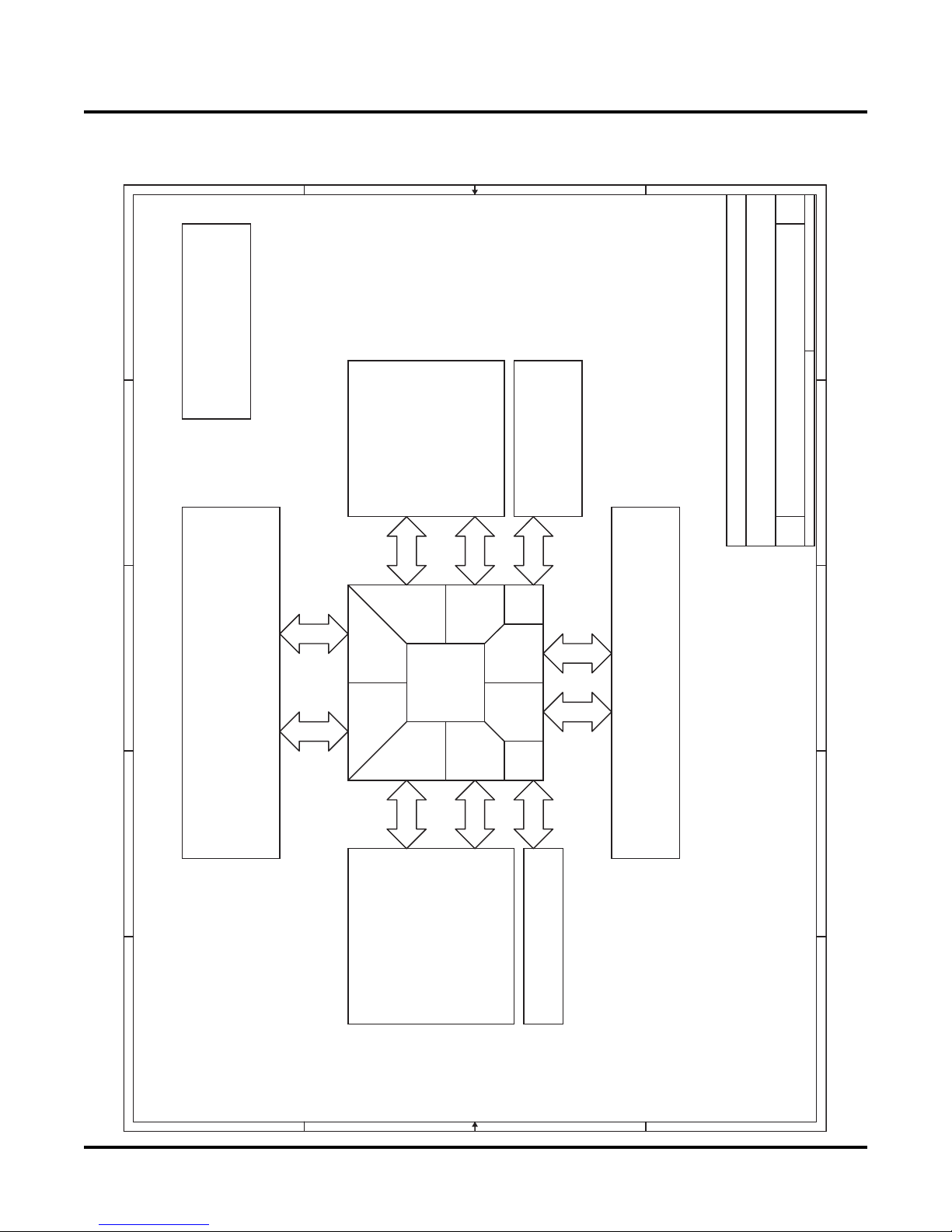
Figure 8. Block Diagram
B
B
B
Rev
Rev
of
of
1
of
1
18
18
18
2
3
(Page 2)
(Page 9)
Power Supply
LCD and
Compact Flash
Connectors
(Page 3)
Area
Prototyping
Bank 2
Bank 1
FPGA
Bank 0
Bank 7
Bank 3
Bank 6
SPI Flash
sysCONFIG
Bank
8
Bank
4
Bank
5
JTAG
Sheet
2
<Doc>
<Doc>
<Doc>
ECP2 Standard -- Block Diagram
ECP2 Standard -- Block Diagram
ECP2 Standard -- Block Diagram
Lattice Semiconductor Corporation
A
A
A
Title
Title
Title
Size Document Number Rev
Size Document Number
Size Document Number
Date: Sheet
Date: Sheet
Date:
3
(Page 4)
64 Bit PCI, PCI-X
LEDs
4
5
RS-232
Seven Seg
D D
Prototyping
Area
Single Ended
SI Testing
Differential
(Page 5)
C C
27
JTAG for FPGA
SI Testing
(Page 6) (Page 6)
B B
4
5
A A
Page 28

LatticeECP2 Standard Evaluation Board
Lattice Semiconductor User’s Guide
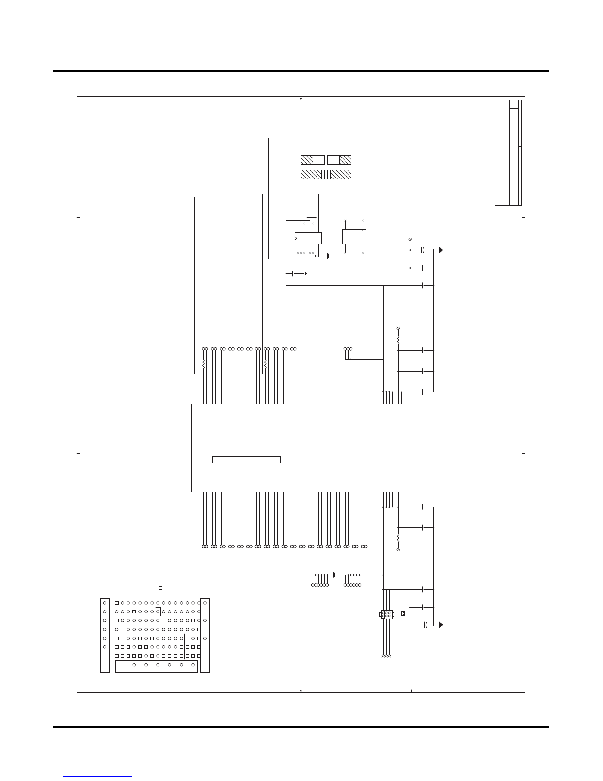
Figure 9. LCD, CF, RS-232, LEDs
D
[8]
C116
C116
0.1uF
VCC_5V
LCD Connector
LCD10LCD_DB7
LCD8LCD_DB3
LCD9
SSEG_B
LCD_DB5
B16
B17
A17
C16
PT44/53/53/62B
PT45/54/54/63B
PT44/53/53/62A
PT45/54/54/63A
0.1uF
LCD_DB5 LCD9
LCD_RS LCD5
LCD_E LCD6
LCD_DB1 LCD7
LCD_DB3 LCD8
LCD_DB7 LCD10
4
14
8
10
6
2
12
16
E
RS
DB7
DB1
DB3
DB5
VDD
CATHODE
ANODE
VO
DB6
VSS
R/W
DB0
DB2
DB4
J42
J42
1
5
3
7
9
15
13
11
LCD_RWLCD0
LCD_DB0
LCD_DB4LCD3
LCD_DB2LCD2
LCD_DB6
LCD4
LCD1
ANODE
R35
R35
2
R34
100
R34
100
1 3
Backlight
LCD1LCD_DB0
LCD2LCD_DB2
LCD3LCD_DB4
LCD4LCD_DB6
LCD5LCD_RS
LCD6
LCD7
LCD_DB1
LCD_E
C17
E16
D16
G16
G15
B18
A18
PT46/55/55/64A
PT46/55/55/64B
PT47/56/65/74A
PT47/56/65/74B
PT48/57/66/75B
PT49/58/67/76B
PT48/57/66/75A
PT49/58/67/76A
LCD[10..0]
18
CATHODE
ANODE
LCD_Connector
LCD_Connector
17
2
1 3
20K
20K
1
GND18
GND18
OPTREX 51505 or Equiv. use pins 1-16
LUMEX or Equiv. use pins 4-18
Contrast
LCD0LCD_RW
TP_A21TP_A2 1
TP_A19TP_A1 9
TP_C18TP_C18
TP_D17TP_D17
A20
D17
A21
C18
A19
PT50/59/68/77B
PT51/60/69/78A
PT50/59/68/77A
PT51/60/69/78B
TP_B21TP_B2 1
TP_B22TP_B2 2
TP_C20TP_C20
TP_C19TP_C19
TP_B20TP_B2 0
TP_D18TP_D18
B22
B20
D18
C19
E18
C20
B21
PT52/61/70/79A
PT53/62/71/80A
PT54/63/72/81B
PT52/61/70/79B
PT53/62/71/80B
PT54/63/72/81A
VREF1_1/PT55/64/73/82A
VREF2_1/PT55/64/73/82B
HEADER 1
HEADER 1
VCC_3.3V
G11
G14
G13
G12
VCCO1
VCCO1
VCCO1
VCCO1
Pad Name = PT{12/22/35/50}
Pad Name = PT{12/22/35/50}
B(Pin 12)
1
GND17
1
151413
16
VCC_3.3V
SW1
SW1
1
23456
R63
10K
R63
10K
R64
10K
R64
10K
R67
R67
10K
10K
R69
10K
R69
10K
10K
10K
R92
R92
R94
10K
R94
2
3
10K
R96
10K
R96
10K
R98
10K
R98
10K
SW6
SW5
SW7
GND17
HEADER 1
HEADER 1
A(Pin 1)
9
121110
SW DIP-8
861milX425mil
SW DIP-8
861milX425mil
7
8
R97 470R97 470
R95 470R95 470
R66 470R66 470
R68 470R68 470
R99 470R99 470
D7D7
D6D6
D8LED_Green D8LED_Green
LED6
LED5
SW3
SW4
LED7
SW2
SW1
SW0
SW[7:0]
R65 470R65 470
R70 470R70 470
R93 470R93 470
D2D2
D1D1
D5D5
D3D3
D4D4
LED4
LED3
LED2
LED1
LED0
SW7
SW6
SW5
SW4
SW3
SW2
SW1
D12
A12
E12
B12
C12
D13
A11
PT31/40/40/49A
PT31/40/40/49B
PT33/42/42/51B
PT33/42/42/51A
PCLKT1_0/PT30/39/39/48A
PCLKC1_0/PT30/39/39/48B
G(Pin 11)
F(Pin 2)
CC0603
CC0603
C93
0.1uF
C93
0.1uF
U2
U2
cathode A
cathode F2annode13NC1
VCC_3.3V
1
4
R103 470R103 470
R102 470R102 470
LED[7:0]
SW0
LED7
LED6
LED5
LED4
LED3
LED2
B13
A13
E14
D14
E13
F14
C13
PT34/43/43/52B
PT34/43/43/52A
PT35/44/44/53A
PT35/44/44/53B
PT36/45/45/54A
PT36/45/45/54B
PT37/46/46/55A
PT37/46/46/55B
NC25NC36cathode E
LED1
A14
7
R104 470R104 470
LED0
B14
PT39/48/48/57B
PT39/48/48/57A
cathode D8cathode DP9cathode C10cathode G11NC4
R110 470R110 470
R112 470R112 470
R111 470R111 470
SSEG_A
SSEG_F
A15
B15
PT40/49/49/58A
13
12
R108 470R108 470
R109 470R109 470
SSEG_E
SSEG_D
E15
F15
PT40/49/49/58B
PT42/51/51/60A
C(Pin 10)
D(Pin 8)
E(Pin 7)
cathode B
annode2
738milX386mil
738milX386mil
14
Seven Segment LED
Seven Segment LED
SSEG_DP
SSEG_C
SSEG_G
A16
D15
C15
PT43/52/52/61A
PT42/51/51/60B
PT43/52/52/61B
DP(Pin 9)
User Defined
470
470
R113
R113
R114
10K
R114
10K
VCC_3.3V
A
B1
A1
SW PUSHBUTTON
SW PUSHBUTTON
SW3
SW3
A1 B1
A2 B2
LED_YellowD9LED_Yellow
D9
SizeB
SizeB
C49
C49
10uF
10uF
+
+
CC0402
CC0402
C83
0.1uF
C83
0.1uF
CC0402
CC0402
C53
0.1uF
C53
0.1uF
CC0402
CC0402
C48
0.1uF
C48
0.1uF
B
B
B
of
of
of
28
28
28
Sheet
Sheet
Sheet
1
<Doc>
<Doc>
<Doc>
ECP2 Standard -- LCD, CF, RS-232, LEDs
ECP2 Standard -- LCD, CF, RS-232, LEDs
ECP2 Standard -- LCD, CF, RS-232, LEDs
Lattice Semiconductor Corporation
C
C
C
Title
Size Document Number Rev
Date:
Title
Size Document Number Rev
Date:
Title
Size Document Number Rev
A2 B2
C102
C102
1uF
1uF
Date:
CC0603
CC0603
2
3
BANK0 BANK1(1 of 6)
BANK0 BANK1(1 of 6)
U3A
U3A
PT3/3/3/3A
PT5/5/5/5B
PT2/2/2/2A/VREF1_0C1PT2/2/2/2B/VREF2_0
PT3/3/3/3BD3PT4/4/4/4AH7PT4/4/4/4BJ7PT5/5/5/5A
PT6/6/6/6AC4PT6/6/6/6BD4PT7/7/7/7AD6PT7/7/7/7BD5PT8/8/8/8AF7PT8/8/8/8BE7PT9/9/9/9AD7PT9/9/9/9BF8PT10/10/10/10A
B2
B1
D1
C2
CF45 CF_D10
CF42 CF_BVD1
CF21 CF_WP
CF44 CF_D09
CF20 CF_D02
CF22 CF_CD2
CF43 CF_D08
RS232_OUTDAT
RS232_CTS
RS232_RTS
RS232_INDAT
VCC_3.3V
C37
C37
CC0603
CC0603
0.1uF
10
3
7
T2IN
R1OUT12R2OUT
J1J1
8
CTSTDRTS
0.1uF
9
16
VCC
GND
8
15
3
1
2
JB1 JB LOCKJB1 JBLOCK
594
DB9J2DB9
SGNDRIDTR
NorComp 190-009-262-001
or Equiv.
MAX3232
MAX3232
JB2 JB LOCKJB2 JBLOCK
4
5
RS-232
D
C38
C38
C36
C36
CC0603
CC0603
CC0603
CC0603
0.1uF
0.1uF
0.1uF
0.1uF
1
4
3
5
11
C1-
C2-
C2+
U1
U1
RS-232
RS-232
C33
C33
C1+
V+2V-
T1IN
T1OUT14T2OUT7R1IN13R2IN
6
C34
C34
0.1uF
CC0603
0.1uF
CC0603
0.1uF
CC0603
0.1uF
CC0603
123
J3J3
1
2
6
J2
DCE
1 to 2 for straight wired cable (default)
2 to 3 for null cable (wires 2 and 3 swapped)
RD
DCD
DSR
PT10/10/10/10B
PT12/21/21/30A
PT14/23/23/32A
PT15/24/24/33A
PT11/20/20/29AE8PT11/20/20/29B
PT12/21/21/30BA3PT13/22/22/31AA4PT13/22/22/31B
B3
CF40 CF_REG
CF18 CF_D00
CF39 CF_INPACK
CF17 CF_A00
CF41 CF_BVD2
CF19 CF_D01
C C
A5
A2
C3
CF16 CF_A01
E9
G8
CF35 CF_CSEL
CF13 CF_A04
CF36 CF_VS2
CF37 CF_RESET
CF15 CF_A02
CF38 CF_WAIT
CF14 CF_A03
PT17/26/26/35B
PT14/23/23/32B
PT15/24/24/33B
PT16/25/25/34AB5PT16/25/25/34BB6PT17/26/26/35A
PT18/27/27/36A
PT18/27/27/36B
CF33 CF_WE
CF10 CF_A07
C6
C7
CF31 CF_IORD
CF9 CF_A08
CF32 CF_IOWR
VCC_3.3V
PT20/29/29/38AD8PT20/29/29/38BC8PT21/30/30/39AA6PT21/30/30/39BB7PT23/32/32/41AB9PT23/32/32/41BB8PT24/33/33/42AA7PT24/33/33/42BA8PT25/34/34/43A
E10
D10
CF29 CF_CE2
CF7 CF_OE
CF30 CF_VS1
CF8 CF_A09
100K
100K
R47
R47
100K
100K
R58
R58
47K
47K
R54
R54
47K
47K
R56
R56
47K
47K
R48
R48
47K
47K
R53
R53
100K
100K
R55
R55
100K
100K
R57
R57
100K
100K
R50
R50
100K
100K
R49
R49
F9
D9
F10
CF11 CF_A06
CF34 CF_READY
CF12 CF_A05
PT25/34/34/43B
PT26/35/35/44A
PT26/35/35/44B
F11
E11
C10
C11
CF6 CF_A10
CF28 CF_D15
CF5 CF_CE1
CF22
CF_CD2
CF23CF38
CF_CD1
CF_WAIT
CF34
CF_READY
CF21
CF_WP
CF39CF36
CF_INPACK
CF_VS2
CF30
CF_VS1
CF41
CF_BVD2
CF42
CF_BVD1
B B
CF27 CF_D14
CF[45..0]
CF3 CF_D06
CF26 CF_D13
CF4 CF_D07
VCC_3.3V
[8]
CF24 CF_D11
CF2 CF_D05
CF25 CF_D12
CF_D12 CF25
CF_D11 CF24
CF_CD1 CF23
26
D1127D1228D1329D1430D15
CD1
J12
J12
D032D043D054D065D076OE/OE/ATASEL
GND1CE1/CE1/CS07A108VCC
CF_D03
CF_D04
CF0
CF1
C40
0.1uF
C40
0.1uF
C41
0.1uF
C41
0.1uF
PT28/37/37/46A/PCLKT0_0
PT27/36/36/45AA9PT27/36/36/45B
A10
B10
B11
CF23 CF_CD1
CF0 CF_D03
CF1 CF_D04
CF_D15 CF28
CF_D14 CF27
CF_D13 CF26
CF_CE2 CF29
32
31
CF_D06CF3
CF_D07
CF_D05
CF_CE1
CF2
CF4
CF5
VCCO0
VCCO0
VCCO0H8VCCO0
PT28/37/37/46B/PCLKC0_0
H9
G9
G10
CF_CSEL CF35
CF_READY CF34
CF_WE CF33
CF_IOWR CF32
CF_IORD CF31
CF_VS1 CF30
CF_VS2 CF36
37
35
34
40
33
38
39
36
WE
VS1
VCC
IORD
CSEL
IOWR
CE2/CE2/CS1
READY/IREQ/INTRQ
9
10
13
CF_A10
CF_A08CF9
CF_A07
CF_OECF7
CF_A09CF8
CF_A05CF12
CF_A06CF11
CF6
CF10
Ultra DMA is not
supported
CF_INPACK CF39
CF_WAIT CF38
CF_RESET CF37
43
42
41
VS2
RESET
WAIT/WAIT/IORDY
CF_A04
CF_A03CF14
CF_A02CF15
CF13
ECP2-12/22/35/50-fpBGA484
ECP2-12/22/35/50-fpBGA484
CF_REG CF40
44
REG/REG/DMACK
INPACK/INPACK/DMARQ
CF_A01CF16
CF_BVD1 CF42
CF_BVD2 CF41
46
45
BVD2/SPKR/DASP
A0020A0119A0218A0317A0416A0515A0614A0712A0811A09
CF_D00CF18
CF_A00CF17
CF_D09 CF44
CF_D08 CF43
D0847D0948D10
BVD1/STSCHG/PDIAG
D0021D0122D02
23
CF_D01CF19
CF_D02
CF20
C43
10uF
C43
10uF
+
+
GND16
GND16
CF_D10 CF45
50
49
GND
PC Card Memory Mode/
PC Card Memory Mode/
WP/IOIS16/IOCS16
CD2
24
25
CF_WPCF21
CF_CD2CF22
0.1uF
SizeB
SizeB
1
HEADER 1
HEADER 1
PC Card I/O Mode/
True IDE Mode
PC Card I/O Mode/
True IDE Mode
Compact_Flash_Connector
Compact_Flash_Connector
Compact Flash Connector
Traces from the ECP2 to
the CF connector must
be less than 6 inches
A
4
5
CC0402
CC0402
C103
C103
0.1uF
28
Page 29
LatticeECP2 Standard Evaluation Board
Lattice Semiconductor User’s Guide
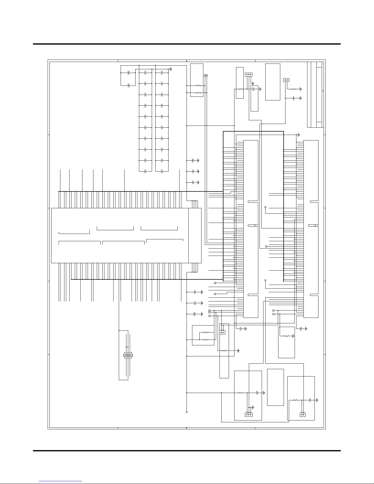
Figure 10. Prototyping Area
D
To PCLK
1
2
4 pin
Osc.
oscillator aligned
Default is a 14 pin
pin 1 to pin 1
14 pin
Osc.
11
161514
VCC_3.3V
Y1
123
CC0603
CC0603
C104
C104
0.1uF
0.1uF
131211
456
To PLL
5
2
(Default)
OSC_PCLK
OSC_PLLCLK
10
9
Y4
(33.33 MHz OSC Installed)
DIP16Y1DIP16
Oscillator Socket
7
8
14
Vcc
NC1GND
relative to the
socket
Oscillator position
8
CLK
OSC14AY4OSC14A
33.33 MHz Oscillator
7
[8]
VCC_3.3V
SizeB
SizeB
C101
10uF
C101
10uF
+
+
CC0402
CC0402
C66
C66
0.1uF
0.1uF
CC0402
CC0402
C115
0.1uF
C115
0.1uF
[8]
A
B
B
B
Rev
Rev
Rev
of
of
of
38
38
38
1
<Doc>
<Doc>
<Doc>
ECP2 Standard -- Prototyping Area
ECP2 Standard -- Prototyping Area
ECP2 Standard -- Prototyping Area
Lattice Semiconductor Corporation
C
C
C
Title
Date: Sheet
Size Document Number
Title
Size Document Number
Date: Sheet
Title
Size Document Number
Date: Sheet
2
TP_M19TP _M19
TP_J22TP _J22TP_F18TP_F18
TP_J21TP _J21
TP_K21TP_K2 1
TP_L22TP_L22
TP_K22TP_K2 2
TP_M20TP_M20
TP_H22TP_H22
TP_L21TP_L21
R115 0R115 0
3
4
U3B
U3B
J21
K21
BANK3
BANK3
PCLKT3_0/PR15/21/27/46AH
PCLKC3_0/PR15/21/27/46BH
(2 of 6)
(2 of 6)
BANK2
BANK2
PR2/2/2/2AH/VREF1_2
PR2/2/2/2BH/VREF2_2
E19
D19
TP_D19TP_D19
TP_E19TP_E19
J22
M20
H22
L22
L21
K22
M19
PRNC/24/30/49B
PRNC/24/30/49A
PRNC/23/29/48AH
PRNC/23/29/48BH
VREF2_3/PR16/22/28/47B
VREF1_3/PR16/22/28/47A
PR4/6/12/14AH
PRNC/4/10/12AH
PRNC/4/10/12BH
PR3/5/11/13A
PR3/5/11/13B
PR4/6/12/14BH
F19
F16
F18
E20
D20
C22
C21
TP_F16TP_F16
TP_C21TP_C21
TP_C22TP_C22
TP_D20TP_D20
TP_F19TP_F19
TP_E20TP_E20
TP_P21TP_P2 1
TP_M22TP _M22
TP_N22TP_N22
TP_P22TP_P2 2
TP_P18TP_P1 8
TP_R22TP_R22
TP_R21TP_R21
TP_N19TP_N19
TP_M21TP_M21
M22
M21
N19
PRNC/26/40/59A
PRNC/26/40/59B
GDLLT_IN/PR17/27/41/60AH
GDLLC_IN/PR17/27/41/60BH
DQS Group
DQS Group
PR5/7/13/15A
PRNC/8/14/16AH/RDQS
PRNC/8/14/16BH
PR5/7/13/15B
H19
G19
G17
TP_H19TP_H19
TP_G17TP_G17
TP_G19TP_G19
TP_P19TP_P1 9
TP_N20TP_N20
TP_R20TP_R20
TP_N21TP_N21
R117 0R117 0
N20
N22
N21
P18
R21
R22
P21
R20
P22
P19
PR23/33/47/66A
PR23/33/47/66B
PR22/32/46/65AH
PR22/32/46/65BH
GPLLT_FB/PR21/31/45/64A
GDLLT_FB/PR18/28/42/61A
GPLLC_FB/PR21/31/45/64B
GDLLC_FB/PR18/28/42/61B
GPLLT_IN/PR20/30/44/63AH
GPLLC_IN/PR20/30/44/63BH
PRNC/9/15/17A
PRNC/9/15/17B
PRNC/10/16/18BH
PRNC/11/17/19B
PR6/12/18/37BH
PRNC/10/16/18AH
PRNC/11/17/19A
PRNC/NC/NC/25A/SPLLT_IN
F20
TP_F20TP_F20
PRNC/NC/NC/25B/SPLLC_IN
F21
E21
E22
H20
D22
H18
G20
TP_G20TP_G20
TP_D22TP_D22
TP_E21TP_E21
TP_H18TP_H18
TP_H20TP_H20
TP_E22TP_E22
TP_F21TP_F21
PR8/14/20/39AH
PRNC/NC/NC/26A/SPLLT_FB
PRNC/NC/NC/26B/SPLLC_FB
PR6/12/18/37AH
PR7/13/19/38A
PR7/13/19/38B
J19
J18
K20
H17
H21
H16
G21
TP_H16TP_H16
TP_J19TP _J19
TP_H17TP_H17
TP_G21TP_G21
TP_J18TP _J18
TP_K20TP_K20
TP_H21TP_H21
TP_VCC9TP_V CC9
TP_VCC7TP_V CC7
TP_VCC8TP_V CC8
(VCCIO3)
DQS Group
DQS Group
PR8/14/20/39BH
PR10/16/22/41AH/RDQS
PR11/17/23/42B
PR12/18/24/43BH
PR9/15/21/40A
PR9/15/21/40B
J17
F22
G22
TP_J17TP _J17
TP_F22TP_F22
TP_G22TP_G22
PR13/19/25/44A/PCLKT2_0
PR10/16/22/41BH
PR11/17/23/42A
PR12/18/24/43AH
PR13/19/25/44B/PCLKC2_0
L18
L19
L17
L20
K19
K18
K17
M18
TP_L20TP_L20
TP_K19TP_K19
TP_K18TP_K18
TP_L19TP_L19
TP_L18TP_L18
TP_L17TP_L17
TP_M18TP_M18
TP_K17TP_K17
L16
M16
P16
N16
VCCO3
VCCO3
VCCO3
Pad Name = PR{12/22/35/50} PRnnxH = True LVDS
Pad Name = PR{12/22/35/50} PRnnxH = True LVDS
VCCO2
VCCO2
VCCO2
J15
K16
H14
H15
VCCIO2
R116 10R116 10
C97
C97
0.1uF
0.1uF
CC0603
CC0603
C98
C98
0.01uF
0.01uF
CC0603
CC0603
N17
N18
C84
C84
5.6nF
5.6nF
CC0603
VCCO3
PLLVCC
VCCO2
PLLVCC
J16
R119 10R119 10
VCC_1.2V VCC_1.2V
CC0603
PLLCAP
ECP2-12/22/35/50-fpBGA484
ECP2-12/22/35/50-fpBGA484
C96
C96
0.01uF
0.01uF
CC0603
CC0603
C105
C105
0.1uF
0.1uF
CC0603
CC0603
3
4
[8]
CC0402
= Unconnected, Plated Holes
Prototype Area
Map
CDEFGHJ
A
B
22
2120
5
191817
KLMNP
R
TP_GND1TP_GND1
TP_GND4TP_GND4
TP_GND3TP_GND3
TP_GND6TP_GND6
TP_GND2TP_GND2
TP_GND5TP_GND5
TP_VCC5TP_V CC5
TP_VCC6TP_V CC6
TP_VCC1TP_V CC1
TP_VCC3TP_V CC3
TP_VCC4TP_V CC4
TP_VCC2TP_V CC2
(VCCIO2)
246
J37
J37
HEADER 3X2
HEADER 3X2
135
CC0402
C74
0.1uF
C74
0.1uF
CC0402
CC0402
C77
0.1uF
C77
0.1uF
SizeB
SizeB
C110
C110
10uF
10uF
JB5 JBLOCKJB5 JBLOCK
+
+
5
16
GND
VCCIO2
D
VCCIO3
VCC_1.2V
VCC_ADJ
VCC_3.3V
VCC_1.2V
VCC_3.3V
VCC_ADJ
[8]
C C
B B
A
29
Page 30
LatticeECP2 Standard Evaluation Board
Lattice Semiconductor User’s Guide
Figure 11. 64-Bit PCI, PCI-X
1
2
3
4
PCI_AD13
U12
BANK4
BANK4
PCLKT4_0/PB31/40/40/49A
(3 of 6)
(3 of 6)
BANK5
BANK5
PB2/2/2/2A/VREF2_5Y3PB3/3/3/3AW4PB4/4/4/4AW5PB5/5/5/5A
U3C
U3C
PCI_REQ_N
PCI_ACK64_N
PCI_CBE0_N
PCI_AD11
PCI_AD9
PCI_AD4
V12
AA13
W12
Y13
Y12
PB32/41/41/50B
PB33/42/42/51B
PB32/41/41/50A
BDQS/PB33/42/42/51A
DQS Group
DQS Group
PCLKC4_0/PB31/40/40/49B
PB2/2/2/2B/VREF1_5Y2PB3/3/3/3BW3PB4/4/4/4BW6PB5/5/5/5B
PCI_AD30
PCIX_ECC2
PCIX_ECC5
PCIX_ECC4
PCIX_ECC3
D
PCI_REQ64_N
PCI_CBE4_N
PCI_AD6
PCI_AD63
PCI_AD0
U13
AA14
U14
AB15
PB34/43/43/52A
PB35/44/44/53A
PB35/44/44/53B
PB34/43/43/52B
PB6/6/6/6A/BDQS
PB6/6/6/6B
Y4
AB3
AA3
AB2
PCI_AD27
PCI_AD29
PCI_AD31
PCI_RST_N
PCI_CBE7_N
PCI_AD59
PCI_AD55
AB16
AB17
PB36/45/45/54A
PB36/45/45/54B
DQS GroupDQS Group
DQS GroupDQS Group
PB7/7/7/7A
PB7/7/7/7B
AB5
AB4
PCI_AD25
PCI_AD23
PCI_AD62
PCI_AD61
PCI_AD60
PCI_AD51
PCI_AD47
PCI_AD2
W14
W13
PB37/46/46/55A
PB37/46/46/55B
PB8/8/8/8A
PB8/8/8/8BY5PB9/9/9/9B
AA5
PCI_CBE3_N
PCI_GNT_N
PCI_AD53
PCI_AD57
AA16
AA15
AB18
V14
AB19
AA17
Y15
W15
PB39/48/48/57A
PB40/49/49/58A
PB41/50/50/59A
PB39/48/48/57B
PB40/49/49/58B
PB42/51/51/60B
PB41/50/50/59B
BDQS/PB42/51/51/60A
PB12/21/21/30A
PB12/21/21/30B
PB9/9/9/9A
PB11/20/20/29A
PB13/22/22/31A
PB11/20/20/29B
PB13/22/22/31B
Y6
Y7
W7
W8
AB7
AA6
AB6
AA7
PCI_AD21
PCI_AD19
PCI_AD24
PCI_AD22
PCI_AD17
PCI_AD28
PCI_AD26
PCI_CBE2_N
PCI_CBE5_N
PCI_AD45
PCI_AD41
U15
AB21
AB20
PB43/52/52/61A
PB43/52/52/61B
PB14/23/23/32AU8PB15/24/24/33A/BDQSW9PB16/25/25/34A
PB14/23/23/32BU9PB15/24/24/33BV9PB16/25/25/34B
PCI_AD16
PCI_INT_N
PCI_IDSEL
J19
J19
+
+
10uF
10uF
C7
C7
SizeB
SizeB
+
+
10uF
10uF
C12
C12
SizeB
SizeB
PCI Decoupling
PCI_AD58
PCI_AD50
PCI_AD52
PCI_AD49
Y16
AA18
U16
W16
PB44/53/53/62A
PB45/54/54/63A
PB44/53/53/62B
PB45/54/54/63B
Y8
AA8
W10
PCI_AD18
PCI_AD20
PCI_PERR_N
PCI_STOP_N
PCI_INTA_N
PCI_INTC_N
246
HEADER 3X2
HEADER 3X2
1
3
5
TP14TP14
C60
C60
C114
C114
0.1uF
0.1uF
0.1uF
0.1uF
CC0603
CC0603
CC0603
CC0603
C59
C59
C58
C58
C8
C8
C6
C6
C113
C113
C11
C11
C90
C90
C100
C100
C51
C51
C112
C112
PCI_AD56
PCI_AD43
PCI_AD37
PCI_AD39
V16
AA21
AA22
AA20
PB46/55/55/64A
PB48/57/66/75A
PB46/55/55/64B
PB48/57/66/75B
PB17/26/26/35A
PB18/27/27/36A
PB17/26/26/35B
PB18/27/27/36B
V10
AB8
AB9
AA9
PCI_TRDY_N
PCI_IRDY_N
PCI_SERR_N
PCI_CBE1_N
0.1uF
0.1uF
0.1uF
0.1uF
0.1uF
0.1uF
0.1uF
0.1uF
0.1uF
0.1uF
0.1uF
0.1uF
0.1uF
0.1uF
0.1uF
0.1uF
0.1uF
0.1uF
0.1uF
0.1uF
PCI_AD36
V17
PB49/58/67/76A
PB20/29/29/38A
AB10
PCI_AD12
CC0603
CC0603
CC0603
CC0603
C52
C52
0.1uF
0.1uF
CC0603
CC0603
CC0603
CC0603
C109
C109
0.1uF
0.1uF
CC0603
CC0603
CC0603
CC0603
C50
C50
0.1uF
0.1uF
CC0603
CC0603
CC0603
CC0603
C5
C5
0.1uF
0.1uF
CC0603
CC0603
CC0603
CC0603
C3
C3
0.1uF
0.1uF
CC0603
CC0603
CC0603
CC0603
C4
C4
0.1uF
0.1uF
CC0603
CC0603
CC0603
CC0603
C108
C108
0.1uF
0.1uF
CC0603
CC0603
CC0603
CC0603
C107
C107
0.1uF
0.1uF
CC0603
CC0603
CC0603
CC0603
PCI_AD44
PCI_AD40
PCI_AD38
PCI_AD48
Y19
Y20
Y18
Y17
PB50/59/68/77A
PB49/58/67/76B
PB50/59/68/77B
PB51/60/69/78B
BDQS/PB51/60/69/78A
PB21/30/30/39A
PB22/31/31/40A
PB20/29/29/38B
PB21/30/30/39B
PB22/31/31/40B
Y10
U10
U11
AA10
PCI_AD14
PCI_PAR
PCI_FRAME_N
PCI_DEVSEL_N
PAR64
PCI_AD42
PCI_AD34
PCI_AD32
PCI_AD33
PCI_AD35
PCI_AD46
PCI_AD54
U18
Y21
W18
Y22
T15
T16
W17
V18
PB53/62/71/80A
PB52/61/70/79B
PB53/62/71/80B
PB54/63/72/81B
PB52/61/70/79A
PB54/63/72/81A
DQS GroupDQS Group
DQS GroupDQS Group
VREF2_4/PB55/64/73/82A
VREF1_4/PB55/64/73/82B
DQS Group
DQS Group
PB23/32/32/41A
PB24/33/33/42A/BDQS
PB25/34/34/43A
PB26/35/35/44A/PCLKT5_0
PB23/32/32/41B
PB24/33/33/42B
PB25/34/34/43B
PB26/35/35/44B/PCLKC5_ 0
Y11
W11
AB11
AB12
AB13
AA11
AA12
AB14
PCI_AD15
PCI_AD7
PCI_AD10
PCI_AD8
PCI_AD5
PCI_AD3
PCI_AD1
PCI_CBE6_N
TP8TP8
R106
R106
5.6K
5.6K
Load for Master Only
R107
5.6K
R107
5.6K
VCC_3.3V
SizeB
SizeBC99
C45
10uF
C45
10uF
+
+
CC0402
CC0402
C10
0.1uF
C10
0.1uF
CC0402
CC0402
C92
0.1uF
C92
0.1uF
T13
T12
T14
R14
VCCO4
VCCO4
VCCO4
VCCO4
Pad Name = PB{12/22/35/50}
Pad Name = PB{12/22/35/50}
ECP2-12/22/35/50-fpBGA484
ECP2-12/22/35/50-fpBGA484
VCCO5
VCCO5T9VCCO5
VCCO5
R9
T10
T11
CC0402
CC0402
0.1uF
0.1uF
C61
C61
CC0402
CC0402
0.1uF
0.1uF
C99
SizeB
SizeB
C9
10uF
C9
10uF
+
+
R61
R61
5.6K
5.6K
R60
R60
5.6K
5.6K
TP9TP9
TP13TP13
TP11TP11
TP10TP10
Load for Master Only
PCI_AD[63:0]
PAR64
PCI_CBE5_N
PCI_CBE7_N
PCI_REQ64_N
PCI_CBE0_N
PCI_PAR
PCI_SMBDAT
PCI_SMBCLK
PCI_STOP_N
PCI_TRDY_N
PCI_FRAME_N
PCI_IDSEL
PCI_GNT_N
PCI_RST_N
PCIX_ECC3
PCIX_ECC5
PCI_INTC_N
PCI_INTA_N
1
2
HEADER 2
HEADER 2
J13
J13
5.6K
5.6K
R59
R59
VCC_3.3V
PCI_AD32
PCI_AD34
PCI_AD36
PCI_AD38
PCI_AD40
PCI_AD42
PCI_AD44
PCI_AD46
PCI_AD48
PCI_AD50
PCI_AD52
PCI_AD54
PCI_AD56
PCI_AD58
PCI_AD60
PCI_AD62
PCI_AD0
PCI_AD2
PCI_AD4
PCI_AD6
PCI_AD9
PCI_AD11
PCI_AD13
PCI_AD15
PCI_AD16
PCI_AD18
PCI_AD20
PCI_AD22
PCI_AD24
PCI_AD26
PCI_AD28
PCI_AD30
PCI_TDI
PCI_TMS
PCI_TRSTN
1-2 = Target
N/C = Master
J38J38
123
Load for Master Only
R126
R126
5.6K
5.6K
C111
C111
Load for Master Only
PCI_M66EN
Reserved_94
94
Ground_93
93
Reserved_92
92
AD[32]
91
Ground_90
90
AD[34]
89
AD[36]
88
Ground_87
87
AD[38]
86
AD[40]
85
+VIO_84
84
AD[42]
83
AD[44]
82
Ground_81
81
AD[46]
80
79
Ground_78
78
AD[50]
77
AD[52]
76
+VIO_75
75
AD[54]
74
AD[56]
73
Ground_72
72
AD[58]
71
AD[60]
70
Ground_69
69
AD[62]
68
67
+VIO_66
66
65
C/BE[7]#
64
Ground_63
63
+5V_62
62
+5V_61
61
REQ64#
60
+VIO_59
59
AD[00]
58
AD[02]
57
Ground_56
56
AD[04]
55
AD[06]
54
+3.3V_53
53
C/BE#[0]
52
AD[09]
49
Ground_48
48
AD[11]
47
AD[13]
46
+3.3V_45
45
AD[15]
44
PAR
43
Ground_42
42
Reserved_41
41
Reserved_40
40
+3.3V_39
39
STOP#
38
Ground_37
37
TRDY#
36
Ground_35
35
FRAME#
34
+3.3V_33
33
AD[16]
32
AD[18]
31
Ground_30
30
AD[20]
29
AD[22]
28
+3.3V_27
27
IDSEL
26
AD[24]
25
Ground_24
24
AD[26]
23
AD[28]
22
+3.3V_21
21
AD[30]
20
PME#
19
Ground_18
18
GNT#
17
+VIO_16
16
RST#
15
3.3VAUX
14
Reserved_11
11
+VIO_10
10
Reserved_9
9
+5V_8
8
INTC#
7
INTA#
6
+5V_5
5
TDI
4
TMS
3
+12V
2
TRST#
1
C42
C42
0.1uF
0.1uF
CC0603
CC0603
N/C = 66 MHz PCI
2-3 = 33 MHz PCI
1-2 = Master
0.01uF
0.01uF
These 0.01 µF capacitors
CC0603
CC0603
AD[48]/CBE[5]#
PAR64/ECC[7]
[8]
CBE[5]#/AD[48]
TP15TP15
[5]
PCI_CLK PCI_GND_57
J48
J48
PCI/PCI-X 64bit EDGE CON Bottom
PCI/PCI-X 64bit EDGE CON Bottom
must be located within
A
J24
J24
1-2 = 66MHz PCI-X
1
2
HEADER 2
HEADER 2
10K
10K
R88
R88
PCI edge connector pin.
0.25 inches of their
C46
C46
0.01uF
0.01uF
PCI_PCIXCAP
PCI_AD33
PCI_AD35
PCI_AD37
PCI_AD39
PCI_AD41
PCI_AD43
PCI_AD45
PCI_AD47
PCI_AD49
PCI_AD51
PCI_AD53
PCI_AD55
PCI_AD57
PCI_AD59
PCI_AD61
PCI_AD63
PCI_CBE4_N
PCI_CBE6_N
PCI_ACK64_N
PCI_AD1
PCI_AD3
PCI_AD5
PCI_AD7
PCI_AD8
PCI_M66EN
PCI_AD10
PCI_AD12
PCI_AD14
PCI_CBE1_N
PCI_SERR_N
PCI_PERR_N
PCI_PCIXCAP
PCI_DEVSEL_N
PCI_IRDY_N
PCI_CBE2_N
PCI_AD17
PCI_AD19
PCI_AD21
PCI_AD23
PCI_CBE3_N
PCI_AD25
PCI_AD27
PCI_AD29
PCI_AD31
PCI_REQ_N
PCI_CLK
PCIX_ECC2
PCI_PRSNT2_N
PCIX_ECC4
PCI_PRSNT1_N
PCI_INTD_N
PCI_INTB_N
TP17TP17 TP12TP12
PCI_TDO
TP16TP16
PCI_TCK
R1
5.6KR15.6K
Load for Master Only
B
B
B
Rev
of
of
of
48
48
N/C = 133 MHz PCI-X
CC0603
CC0603
94
93
92
91
90
89
88
87
86
85
84
83
82
81
80
79
78
77
76
75
74
73
72
71
70
69
68
67
66
65
64
63
62
61
60
59
58
57
56
55
54
53
52
49
48
47
46
45
44
43
42
41
40
39
38
37
36
35
34
33
32
31
30
29
28
27
26
25
24
23
22
21
20
19
18
17
16
15
14
11
10
9
8
7
6
5
4
3
2
1
C1
C1
0.1uF
0.1uF
48
Sheet
Sheet
1
<Doc>
<Doc>
<Doc>
ECP2 Standard -- 64 Bit PCI, PCI-X
ECP2 Standard -- 64 Bit PCI, PCI-X
ECP2 Standard -- 64 Bit PCI, PCI-X
Lattice Semiconductor Corporation
C
C
C
Title
Size Document Number
Date: Sheet
Title
Size Document Number Rev
Date:
Title
Size Document Number Rev
Date:
Ground_94
Reserved_93
Reserved_92
Ground_91
AD[33]
AD[35]
+VIO_88
AD[37]
AD[39]
Ground_85
AD[41]
AD[43]
Ground_82
AD[45]
AD[47]
+VIO_79
AD[49]/CBE[4]#
2
AD[51]
Ground_76
AD[53]
AD[55]
Ground_73
AD[57]
AD[59]
+VIO_70
AD[61]
AD[63]
Ground_67
CBE[4]#/AD[49]
C/BE[6]#
Ground_64
Reserved_63
+5V_62
+5V_61
ACK64#
+VIO_59
AD[01]
Ground_57
AD[03]
AD[05]
+3.3V_54
AD[07]
AD[08]
M66EN
AD[10]
AD[12]
Ground_46
AD[14]
C/BE#[1]
+3.3V_43
SERR#
+3.3V_41
PERR#
3
LOCK#
Ground_38
DEVSEL#
+3.3V_36
IRDY#
Ground_34
C/BE#[2]
AD[17]
+3.3V_31
AD[19]
AD[21]
Ground_28
AD[23]
C/BE#[3]
+3.3V_25
AD[25]
AD[27]
Ground_22
AD[29]
AD[31]
+VIO_19
REQ#
Ground_17
CLK
Ground_15
Reserved_14
PRSNT2#
Reserved_10
PRSNT1#
INTD#
INTB#
+5V_7
+5V_5
TDO
Ground_3
TCK
-12V
PCI/PCI-X 64bit EDGE CON Top
PCI/PCI-X 64bit EDGE CON Top
J14
J14
4
CC0603
CC0603
5
D
PCI_INTB_N
PCI_INTD_N
VCC_3.3V
[8]
C C
Load for Master Only
VCC_3.3V
B B
PCI_PRSNT1_N
R51
5.6K
R51
5.6K
123
J9J9
Load for Master Only
C39
C39
0.01uF
0.01uF
CC0603
CC0603
1-2 = Master
2-3 = Target
N/C = Target
Load for Master Only
R62
5.6K
R62
5.6K
0.25 inches of their
PCI edge connector pin.
These 0.01 µF capacitors
must be located within
1-2 = Master
N/C = Target
A
PCI_PRSNT2_N
1
2
J23
J23
5
C47
C47
0.01uF
0.01uF
CC0603
CC0603
HEADER 2
HEADER 2
30
Page 31
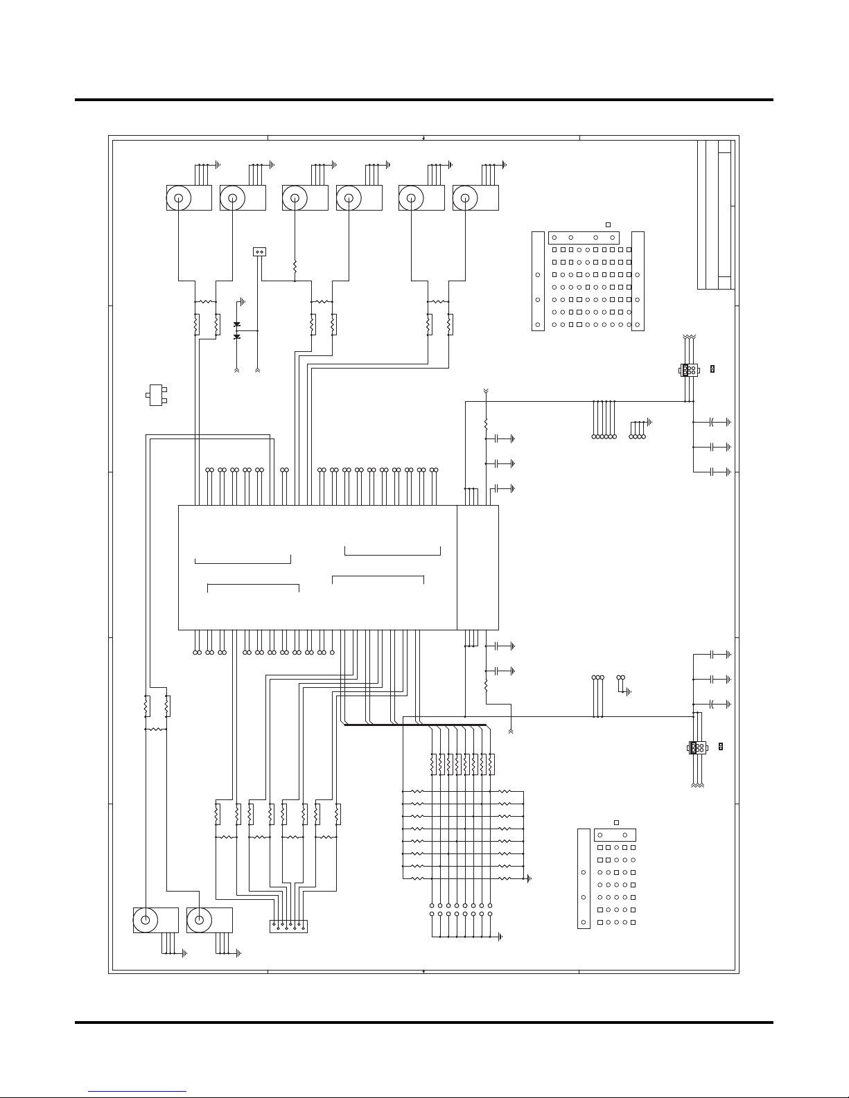
LatticeECP2 Standard Evaluation Board
Lattice Semiconductor User’s Guide
Figure 12. SI Testing
D
3
2
5
4
J26
J26
1
1
50 ohm SMA Connectors
Diff pair, equal length, 50 ohms
R86
DNL
R86
DNL
R84 DNLR84 DNL
close to the FPGA
Place resistor trio as
as possible
J25
J25
SMA Connector
SMA Connector
1
13
R85 DNLR85 DNL
D20
D20
3
4
2
5
SMA Connector
SMA Connector
J21
J21
J22
J22
1
2
HEADER 2
HEADER 2
Add jumper if using PCI or PCI-X
2
Place pad for header pin 2
directly on the trace to
avoid a stub.
BAS70-04
BAS70-04
5
2
3
4
SMA Connector
SMA Connector
1
R27 0R27 0
Diff pair, equal length, 50 ohms
DNL
DNL
R30
R30
R28 DNLR28 DNL
R29 DNLR29 DNL
as possible
Place resistor trio as
close to the FPGA
2
2
345
J20
J20
SMA Connector
SMA Connector
1
345
2
J15
J15
1
3
4
5
J16
J16
SMA Connector
SMA Connector
SMA Connector
SMA Connector
1
Plated Holes
= Unconnected,
Prototype Area
Map
GND
7
VCCIO6
6
Diff pair, equal length, 50 ohms
R91
DNL
R91
DNL
R89 DNLR89 DNL
R90 DNLR90 DNL
Place resistor trio as
close to the FPGA
as possible
54
321
MNPRTUV
W
[8]
2
2
BAS70-04
SOT-23
13
TP_M4TP_M4
TP_M3TP_M3
M6
M4
M5
M3
6KNAB7
6KNAB7
VREF2_6/PL16/22/28/47A
3
PCLKT6_0/PL15/21/27/46AH
PCLKC6_0/PL15/21/27/46BH
(4 of 6)
(4 of 6)
VREF1_6/PL16/22/28/47B
PCI_CLK
VCC_3.3V
[4]
[8]
TP_Y1TP_Y1
TP_U4TP_U4
TP_U3TP _U3
U4
PL27/41/55/74AU3PL27/41/55/74B
DQS Group
DQS Group
TP_V4TP_V4
TP_R7TP_R7
TP_AA1TP_AA1
TP_W1TP_W1
TP_T7TP_T7
TP_V3TP_V3
TP_AA2TP_AA2
T7
AA2
V3
V4
Y1
W1
R7
AA1
PL29/43/57/76A
PL31/45/59/78B
PL29/43/57/76B
PL31/45/59/78A
PL30/44/58/77AH
PL28/42/56/75BH
PL30/44/58/77BH
LDQS/PL28/42/56/75AH
TP_V1TP_V1
TP_T2TP_T2
TP_M2TP_M2
TP_N4TP_N4
TP_N2TP_N2
TP_P5TP_P5
TP_N1TP_N1
TP_M1TP_M1
PLNC/23/29/48AHM2PLNC/23/29/48BH
M1
DQS Group
DQS Group
N1
N2
PLNC/24/30/49B
PLNC/24/30/49A
TP_P4TP_P4
TP_N3TP _N3
TP_N5TP _N5
TP_R4TP _R4
P4
R4
N4
P2
N3
P5
P1
PLNC/26/40/59AN5PLNC/26/40/59B
PLNC/25/39/58BH
LDQS/PLNC/25/39/58AH
GDLLT_FB/PL18/28/42/61A
GDLLC_FB/PL18/28/42/61B
GDLLT_IN/PL17/27/41/60AH
GDLLC_IN/PL17/27/41/60BH
DQS Group
DQS Group
TP_T3TP_T3
TP_U1TP_U1
TP_T5TP_T5
TP_T1TP_T1
R3
T4
R1
T5
T2
R2
PL22/32/46/65AHT1PL22/32/46/65BH
GPLLT_FB/PL21/31/45/64A
GPLLC_FB/PL21/31/45/64 B
GPLLT_IN/PL20/30/44/63AH
GPLLC_IN/PL20/30/44/63BH
TP_T6TP_T6
TP_R6TP _R6
TP_U2TP _U2
TP_V2TP_V2
V2
U1
V1
T6
T3
U2
PL23/33/47/66B
PL25/39/53/72A
PL23/33/47/66A
PL25/39/53/72B
PL24/38/52/71BH
PL24/38/52/71AH
PL26/40/54/73AHR6PL26/40/54/73BH
DQS Group
DQS Group
P7
R8
P8
VCCO6
VCCO6N7VCCO6
VCCO6
PLnnxH = True LVDS
PLnnxH = True LVDS
VCC_1.2V
CC0603
CC0603
C56
0.1uF
C56
0.1uF
R101 10R101 10
CC0603
CC0603
C57
C57
0.01uF
0.01uF
CC0603
CC0603
C79
5.6nF
C79
5.6nF
N6
P6
PLLCAP
PLLVCC
TP_VCC11TP_VCC11
(VCCIO6)
TP_VCC10TP_VCC10
TP_VCC12TP_VCC12
TP_VCC14TP_VCC14
TP_VCC1 3TP_ VCC13
TP_VCC1 5TP_ VCC15
A
VCCIO6
B
B
B
of
of
of
58
58
58
Sheet
Sheet
Sheet
1
<Doc>
<Doc>
<Doc>
ECP2 Standard -- SI Testing
ECP2 Standard -- SI Testing
ECP2 Standard -- SI Testing
Lattice Semiconductor Corporation
C
C
C
Title
Size Document Number Rev
Date:
Title
Size Document Number Rev
Date:
Title
Size Document Number Rev
Date:
[8]
VCC_ADJ
VCC_1.2V
Y
AA
TP_GND12TP_GND12
TP_GND13TP_GND13
TP_GND10TP_GND10
TP_GND11TP_GND11
VCC_3.3V
135
J18
J18
JB12 JBLOCKJB12 JBLOCK
HEADER 3X2
HEADER 3X2
246
2
SizeB
SizeB
C44
10uF
C44
10uF
+
+
CC0402
CC0402
C80
C80
0.1uF
0.1uF
CC0402
CC0402
C81
0.1uF
C81
0.1uF
3
4
Place resistor trio as
close to the FPGA
as possible
5
J27
J27
K
K
N
N
A
A
B
B
U3D
U3D
R24
R24
R25DNL R25DNL
DNL
DNL
R26
R26
DNL
DNL
Diff pair, equal length, 50 ohms
1
J28
J28
SMA Connector
SMA Connector
234
5
PLNC/4/10/12AH
PL2/2/2/2/2AH/VREF2_7E4PL2/2/2/2/2BH/VREF1_7
E5
E3
TP_F3TP_F3
TP_E5TP_E5
TP_E3TP_E3
TP_E4TP_E4
Place resistor trio as
1
D
PLNC/4/10/12BHF3PL3/5/11/13AF4PL3/5/11/13BF5PL4/6/12/14AHE2PL4/6/12/14BH
E1
TP_F4TP_F4
TP_F5TP_F5
close to the FPGA
as possible
R14
R14
R15DNL R15DNL
DNL
DNL
R18
R18
DNL
DNL
Diff pair,
equal length,
50 ohms
SMA Connector
SMA Connector
234
5
PL5/7/13/15AG6PL5/7/13/15B
PLNC/8/14/16AH/LDQSH4PLNC/8/14/16BHH5PLNC/9/15/17AF1PLNC/9/15/17BF2PLNC/10/16/18AHG3PLNC/10/16/18BHG4PLNC/11/17/19A
G7
TP_G7TP_G7
TP_H5TP_H5
TP_F2TP_F2
TP_H4TP _H4
TP_F1TP_F1
TP_G6TP_ G6
Place resistor trio as
close to the FPGA
as possible
R16
R16
R17DNL R17DNL
DNL
DNL
R19
R19
DNL
DNL
equal length,
50 ohms
Diff pair,
1
J6A
J6A
PLNC/11/17/19BG2PLNC/NC/NC/25A/SPLLT_IN
PLNC/NC/NC/25B/SPLLC_INJ6PLNC/NC/NC/26A/SPLLT_FBH3PLNC/NC/NC/26B/SPLLC_FBH2PL6/12/18/37AH1PL7/13/19/38AJ4PL7/13/19/38BJ5PL8/14/20/39AHJ2PL8/14/20/39BHJ1PL9/15/21/40A
H6
G1
TP_G3TP_G3
TP_G1TP_G1
TP_H6TP_H6
TP_G2TP_ G2
TP_J6TP_ J6
TP_G4TP_G4
as possible
Place resistor trio as
close to the FPGA
R77DNL R77DNL
R78DNL R78DNL
R80
R80
DNL
DNL
equal length,
50 ohms
Diff pair,
23456
7
8
RJ-45
RJ-45
TP_H3TP_H3
TP_H2TP _H2
TP_H1TP _H1
SI7
SI6
Place resistor trio as
close to the FPGA
as possible
R87DNL R87DNL
R79
R79
DNL
DNL
R81
R81
DNL
DNL
equal length,
Diff pair,
50 ohms
AMP 6368150-1
Vertical Mount
C C
Pad Name = PL{12/22/35/50}
PL9/15/21/40B
PL11/17/23/42BK1PL12/18/24/43AH
PL10/16/22/41AH/LDQSK3PL10/16/22/41BHK4PL11/17/23/42A
PL12/18/24/43BHL3PL13/19/25/44A/PCLKT7_0L2PL13/19/25/44B/PCLKC7_0
L5
L4
L6
K2
SI5
SI4
SI3
SI2
SI[7:0]
L1
SI1
SI0
R83
DNL
R83
DNL
DNL
DNL
R82
R82
R76
R76
DNL
DNL
R75
R75
DNL
DNL
R74
DNL
R74
DNL
R73
DNL
R73
DNL
R72
R72
DNL
DNL
DNL
DNL
R71
R71
Pad Name = PL{12/22/35/50}
SI7
SI6
SI5
R9 DNLR9 DNL
R10 DNLR10 DNL
R8 DNLR8 DNL
TP_SI6TP_SI6
TP_SI5TP_SI5
TP_SI7TP_SI7
TP_GSI5TP_GSI5
TP_GSI6TP_GSI6
TP_GSI7TP_GSI7
SI4
R11 DNLR11 DNL
TP_SI4TP_SI4
TP_GSI4TP_GSI4
ECP2-12/22/35/50-fpBGA484
ECP2-12/22/35/50-fpBGA484
PLLVCC
VCCO7J8VCCO7K7VCCO7L7VCCO7
K6
M7
C55
C55
0.01uF
0.01uF
CC0603
CC0603
C54
C54
VCCIO7 VCCIO6
0.1uF
0.1uF
R100 10R100 10
CC0603
CC0603
SI3
SI2
SI1
SI0
VCC_1.2V
[8]
R22 DNLR22 DNL
R23 DNLR23 DNL
R12 DNLR12 DNL
R13 DNLR13 DNL
R21
DNL
R21
DNL
R20
DNL
R20
DNL
DNLR7DNL
R7
R6
DNLR6DNL
R5
DNLR5DNL
R4
DNLR4DNL
R3
DNLR3DNL
R2
DNLR2DNL
TP_VCC18TP_VCC18
TP_VCC17TP_VCC17
TP_VCC19TP_VCC19
(VCCIO7)
Prototype Area
Map
7
VCCIO7
TP_GND15TP_GND15
TP_GND14TP_GND14
Plated Holes
= Unconnected,
GND
456
TP_SI1TP_SI1
TP_SI0TP_SI0
TP_SI2TP_SI2
TP_SI3TP_SI3
TP_GSI2TP_GSI2
TP_GSI3TP_GSI3
TP_GSI1TP_GSI1
TP_GSI0TP_GSI0
B B
23
1
E
G
J
F
H
A
CC0402
CC0402
C69
0.1uF
C69
0.1uF
CC0402
CC0402
C68
0.1uF
C68
0.1uF
SizeB
SizeB
10uF
10uF
C2
C2
+
+
4
2
4
6
J17
J17
JB11 JBLOCKJB11 JBLO CK
HEADER 3X2
HEADER 3X2
135
VCC_3.3V
VCC_ADJ
VCC_1.2V
[8]
5
31
Page 32

LatticeECP2 Standard Evaluation Board
Lattice Semiconductor User’s Guide
Figure 13. JTAG and sysCONFIG
1
e
d
oM n
o
itarug
i
f
noC2GF
Reserved
SPI Flash (Default)
1(OFF)0(ON) 0(ON)
CFG1 CFG0
0(ON) 0(ON)
0(ON)
C
SPIm Flash
Reserved0(ON) 1(OFF)1(OFF)
1(OFF) 0(ON)
0(ON)
d
evreseR
Slave Serial
0(ON) 0(ON)
0(ON)
)F
F
O(1
1(OFF) 1(OFF)
D
ispJTAG
Reserved
Slave Parallel
1(OFF)1(OFF)1(OFF)
0(ON)
1(OFF)1(OFF)
XXX
Push Button
Program
B1
SW2 SW PUSHBUTTONSW2 SW PUSHBUTTON
A1B1A2 B2
A2 B2
A1
R118
10K
R118
10K
Program
D12
LED_Yellow
D12
LED_Yellow
470
470
R33
R33
PROGRAMN
On When Low
VCC_3.3V
Done
D10
LED_Green
D10
LED_Green
Q1
BSS138LT1Q1BSS138LT1
470
470
R31
R31
On When High
Drain
SOT-23
VCC_3.3V
TP_100TP_100
TP_102TP_102
Gate Source
D11
LED_Red
D11
LED_Red
Initializing
470
470
R32
R32
On When Low
R125
R125
10K
10K
VCC_3.3V
Configur ation Status
TP_103TP_103
A
B
B
B
of
of
of
68
68
68
Sheet
Sheet
Sheet
1
<Doc>
<Doc>
<Doc>
ECP2 Standard -- JTAG & sysCONFIG
ECP2 Standard -- JTAG & sysCONFIG
ECP2 Standard -- JTAG & sysCONFIG
Lattice Semiconductor Corporation
C
C
C
Title
Size Document Number Rev
Date:
Title
Size Document Number Rev
Date:
Title
Size Document Number Rev
Date:
INITN
2
CFG2
CFG1
WRITEN
WRITEN
DOUT
ECP2-12/22/35/50-fpBGA484
ECP2-12/22/35/50-fpBGA484
VCCO8
VCCO8
P15
R15
FPGA_D7
FPGA_D0
VCC_BANK8
CCLK
R121
10K
R121
10K
8
7
6
C
VCC
/HOLD
U4
/S1Q2/W3VSS
14
16
D15C
U5
/HOLD1VCC2N/C13N/C2
FPGA_D6
INITN
DONE
2
468
J40
J40
135
7
VCC_BANK8
FPGA_D6
BUSY
CCLK
J33J33
123
DI
FPGA_D0
4.7K
4.7K
R120
R120
SISPI
CC0603
CC0603
C106
0.1uF
C106
0.1uF
5
D
SPID0
W25P16VSSIGU4W25P16VSSIG
4
9
10
/W
VSS
N/C511N/C612N/C713N/C8
W25P32VSFIGU5W25P32VSFIG
/S7Q
N/C35N/C4
8
4
6
CFG0
PROGRAMN
1012141618
2022242628
303234
9
1113151719212325272931
FPGA_D7
J34J34
33
FPGA_D6
FPGA_D4
FPGA_D2
FPGA_D1
FPGA_D0
CSN
FPGA_D5
FPGA_D3
CS1N
123
JB19 JBLOCKJB19 JBLOCK
JB18 JBLOCKJB18 JBLOCK
VCC_3.3V
FPGA_D7
DOUT
R127
10K
R127
10K
SPIFASTN
1
2
HEADER 2
HEADER 2
J44
J44
JB22
JBLOCK
JB22
JBLOCK
1
GND20
GND20
HEADER 1
HEADER 1
Load one Flash, not both
PROGRAMN
INITN
8
10
246
J41
J41
sysCONFIG
sysCONFIG
Output
HEADER 17X2
HEADER 17X2
2
J32J32
3
1
R123
10K
R123
10K
10K
10K
R122
R122
13579
CCLK
DOUT
FPGA_D[0:7]
J31J31
123
Jumpers normally not installed
C86
C86
C13
C13
10uF
10uF
+
+
Removed = Normal Read (03x)
Note: Not all SPI Serial Flash
Installed = Fast Read (0Bx) (default)
support Fast Read
VCC_BANK8
246
J39
J39
JB7 JBLOCKJB7 JBLOCK
HEADER 3X2
HEADER 3X2
5
1
3
VCC_1.2V
VCC_3.3V
VCC_ADJ
WRITEN
20222426283032
12
141618
1113151719212325272931
FPGA_D7
FPGA_D4
FPGA_D2
FPGA_D1
FPGA_D0
FPGA_D6
FPGA_D5
FPGA_D3
J35
J35
J36
HEADER 2
J36
HEADER 2
1 2
CSON
CC0402
CC0402
0.1uF
0.1uF
SizeB
SizeB
34
HEADER 17X2
HEADER 17X2
33
3
sysCONFIG Connectors
2
HEADER 2
HEADER 2
1
CSON
Jumpers normally not installed
4
5
(5 of 6)
(5 of 6)
U3E
U3E
INITN INITN
2
1
INIT_CHN
J11
J11
Not Installed
Jumper Normally
4.7K
4.7K
JB17
JB17
2
1
PROGRAMN
CFG2
CFG0
CFG1
W20
W19
V19
CFG1
CFG0
CFG2
VCCJ
T8
V6
U5
VCC_3.3V
HEADER 2
HEADER 2
TDO
TDI
JBLOCK
JBLOCK
HEADER 2J8HEADER 2
J8
246
J43
J43
HEADER 3X2
HEADER 3X2
135
JB14 JBLOCKJB14 JBLO CK
JB15 JBLOCKJB15 JBLO CK
JB13 JBLOCKJB13 JBLOCK
2
3
4
CFG1
CFG2
R129 10KR129 1 0K
R128 10KR128 1 0K
1
GND19
GND19
1x10 JTAG Chain
Output Header
3
2
1
J7J7
JB16
JB16
JBLOCK
JBLOCK
t)
JTAG
CFG0
R130 10KR130 1 0K
VCC_3.3V
HEADER 1
HEADER 1
Jumper Normally
J5
123456789
TMS
TDI_CH
TDO_CH
PROGN
10K
10K
R124
R124
TP_101TP_101
J10
J10
HEADER 2
HEADER 2
Not Installed
HEADER 10J5HEADER 10
10
TCK
INIT_CHN
DONE
CCLK
DONE DONE
2
1
PROGN PROGRAMN PROGRAMN
R52
R52
Only One Board
TDO_DL
TDI
TCK
PROGN
INIT_CHN
DONE
TMS
C35
C35
0.1uF
123456789
2 to 3 = Single device or last in the chain (defaul
5
1 to 2 = Multiple devices and not last in the chain
1x10 JTAG Chain
Input Header
10
J4
HEADER 10J4HEADER 10
0.1uF
CC0603
CC0603
VCC_3.3V
PROGRAMN
INITN
DONE
V21
R18
V20
W22
V22
INITN
CCLK
DONE
PROGRAMN
DOUT/CSON/PR71B
VCCJ
VCCJ
TMSV5TDO
PR72A/DI/CSSPIN
TCK
TDI
U7
T22
U20
FPGA_D0
CCLK
TMS
TCK
Have this Jumper
Installed
in the Chain Should
DONE
PR75A/D2
PR76A/D0(MSb)/SPIFASTN
PR75B/D1
T20
U21
U22
FPGA_D1
FPGA_D2
FPGA_D3
C62
C62
0.1uF
0.1uF
R19
BUSY/SISPI/PR71A
PR73B/D5
PR72B/D7(LSb)/SPID0
PR73A/D6
PR74A/D4
PR74B/D3
T19
T17
T21
T18
R17
FPGA_D6
FPGA_D7
FPGA_D4
FPGA_D5
CC0402
CC0402
(Dual Footprint)
SPI Serial Flash
PR76B/CSN
PR77A/CS1N
PR77B/WRITEN
R16
U19
CSSPIN
VCC_BANK8
[8]
D
C C
B B
A
32
Page 33

LatticeECP2 Standard Evaluation Board
Lattice Semiconductor User’s Guide
Figure 14. FPGA Power
of
of
of
78
78
78
1
Lattice Semiconductor Corporation
H13
D2
F17
H11
J14
K12
D21
H12
J20
F6
H10
GND
GND
GND
GND
GND
GND
2
(6 of 6)
(6 of 6)
U3F
U3F
VCC CORE
VCC CORE
VCC CORE
VCC CORE
VCC CORE
VCC CORE
K9
J11
J10
J12
J13
K14
K10
J9
GND
GND
GNDJ3GND
GNDK8GND
GND
GND
VCC CORE
VCC CORE
VCC CORE
VCC CORE
VCC CORE
VCC CORE
VCC CORE
VCC CORE
L9
N9
M9
L14
P10
P11
N14
M14
L12
K13
K15
L8
L11
L10
K11
GND
GND
GND
GND
GND
GND
GND
GND
VCCAUX
VCC CORE
VCCAUX
VCCAUX
VCC CORE
VCCAUX
E6
C5
E17
P12
P13
D11
L13
L15
GND
GND
VCCAUX
VCCAUXG5VCCAUX
F13
M8
G18
M10
GND
K5
M11
M12
GND
GND
VCCAUX
VCCAUX
P17
M17
M15
M13
GND
GND
VCCAUX
VCCAUXR5VCCAUX
V7
N8
GND
GND
VCCAUXV8VCCAUX
N10
V11
N11
GND
V13
N12
N13
GND
GND
VCCAUX
VCCAUX
V15
R12
P20
R11
P3
N15
GND
GND
F12
XRES
U6
Y14
P9
P14
GND
GND
GND
GND
XRES (10K 1% to GND)
R105
R105
10K 1%
10K 1%
W21
W2
R13
U17
R10
GND
GND
A1
Y9
GND
GND
GND
GND
GND
GND
GND
GND
GND
ECP2-12/22/35/50-fpBGA484
GND
GND
GND
GND
A22
AA4
AB1
AA19
ECP2-12/22/35/50-fpBGA484
GND
GNDC9GND
GND
GND
B4
B19
C14
AB22
1
Sheet
Sheet
<Doc> B
<Doc> B
<Doc> B
ECP2 Standard -- FPGA Power
ECP2 Standard -- FPGA Power
ECP2 Standard -- FPGA Power
B
B
B
Title
Date:
Title
Date:
Size Document Number Rev
Size Document Number Rev
Title
Size Document Number Rev
Date: Sheet
2
0.1uF
0.1uF
C87
CC0402
C87
CC0402
CC0402
CC0402
0.1uF
0.1uF
C70
3
VCC_CORE
JB24
JB24
JBLOCK
246
J30
J30
Current Measurement
(remove jumpers,
insert meter)
1
4
5
JBLOCK
JBLOCK
JBLOCK
JB25
JB25
HEADER 3X2
HEADER 3X2
5
3
JBLOCK
JBLOCK
JB26
JB26
VCC_1.2V
[8]
VCC_AUX
2
1
Current Measurement
(remove jumper,
insert meter)
HEADER 2
HEADER 2
VCC_3.3V
[8]
JB27
JB27
J29
J29
JBLOCK
JBLOCK
C70
0.1uF
0.1uF
C71
CC0402
C71
CC0402
C82
CC0402
C82
CC0402
0.1uF
0.1uF
0.1uF
0.1uF
C75
CC0402
C75
CC0402
C85
C85
CC0402
CC0402
0.1uF
0.1uF
0.1uF
CC0402
0.1uF
CC0402
C73
C73
0.1uF
0.1uF
C72
CC0402
C72
CC0402
C76
CC0402
C76
CC0402
0.1uF
0.1uF
SizeB
SizeB
C94
10uF
C94
10uF
+
+
0.1uF
0.1uF
C88
CC0402
C88
CC0402
0.1uF
0.1uF
CC0402
CC0402
C63
C63
C67
0.1uF
CC0402
C67
0.1uF
CC0402
CC0402
CC0402
0.1uF
0.1uF
C91
C91
0.1uF
0.1uF
C78
CC0402
C78
CC0402
CC0402
CC0402
C89
0.1uF
C89
0.1uF
C64
C64
0.1uF
0.1uF
CC0402
CC0402
CC0402
CC0402
0.1uF
0.1uF
C65
C65
SizeB
SizeB
10uF
10uF
C95
C95
+
+
3
4
5
D D
C C
B B
A A
33
Page 34

LatticeECP2 Standard Evaluation Board
Lattice Semiconductor User’s Guide
Figure 15. Power
1
3.3V, 3A
2
1
GND21
GND21
3
10nF
CC0603
10nF
CC0603
C32
C32
D18
BAT54
SOD-123
D18
BAT54
SOD-123
4
VCC_IN
PCI this signal disables the 3.3V
When this board is plugged into
converter. 3.3V will then come
from the PCI bus.
5
VCC_IN
1
S
J46
J46
CONN_RED
CONN_RED
PCI_GND_57
[4]
D
HEADER 1
HEADER 1
L3
L3
Sumida CDRH8D43-100NC
ECJ-1VB1H103K
1
BS
2
VIN
R40
R40
100K
100K
CR0603
CR0603
Banana Jack
5W to 23W
5V DC Only
D
VCC_3.3V
[2,3,4,5,6,7]
2
10uH
10uH
8.3mmX8.3mm
8.3mmX8.3mm
1
3
SW
U6
MP2307U6MP2307
EN7SS
16V
22uF
22uF
C117
C117
C3225X5R1C226M
CC1210
CC1210
SMC
SMC
D19
D19
MBRS340
MBRS340
J47
PWR JACK
J47
PWR JACK
D16
267-05
D16
267-05
1N5820
1N5820
1N5820
267-05
1N5820
267-05
D15
D15
CR0603
CR0603
R38
26.1K 1%
R38
26.1K 1%
5
FB
COMP
PAD
GND
8
X5R
321
5.5mm Barrel, (-)
2.5mm Pin, (+)
T520B476M006ASE070
+
+
C21
C21
SizeB
SizeB
47uF
47uF
R37
CR0603
R37
CR0603
10K 1%
10K 1%
D17
D17
1N5819
1N5819
SOD-123
SOD-123
R39
R39
5.6K
5.6K
4.7nF
4.7nF
CC0603
CC0603
C22
C22
ECJ-2VB1H472K
6
DNL
DNL
C23
CC0603
C23
CC0603
9
4
C24
C24
0.1uF
0.1uF
CC0603
CC0603
protection
Reverse polarity
J45
J45
VCC_ADJ
CR0603
CR0603
Place Switch next to
DC input jack
1
S
CONN_BLACK
CONN_BLACK
Banana Jack
[3,5,6]
1.2V, 3A
Q2
Si5447DCQ2Si5447DC
D
D
8
D
D
7
D
D
6
G4S
5
VCC_3.3V
VCC_IN
VCC_INVCC_IN
Q3
Si5447DCQ3Si5447DC
D
D
1
8
D
D
2
7
D
D
3
6
G4S
5
Adjustable, 1.2V to 2.5V, 3A
C C
R4610R46
U9
U9
VCC_IN
VCC_1.2V
VCC_5V
[2]
[3,5,6,7]
1uF
1uF
SizeA
SizeA
C16
C16
+
+
+
+
C18
C18
SizeD
SizeD
100uF
100uF
2
6.2uH
6.2uH
L2
7mmX7mm
L2
7mmX7mm
1
2
1
3
D13
B320A
D13
B320A
SMA
SMA
R4210R42
10
C28
1800pF
CC0603
C28
1800pF
CC0603
DRAIN_1.2
100
100
R43
R43
4
6
5
CR0805
SW
U8
U8
/EN1GND2FB
+
+
C29
C29
SizeC
SizeC
10uF
10uF
CR0805
VIN
ISENSE
SOT23-6
SOT23-6
TPS64203DVB
TPS64203DVB
3
U7
5V, 300mA
C15
CC1812
C15
CC1812
22uF
22uF
10uF
CC1210
10uF
CC1210
X7R X5RX7R
C17
C17
LMK325BJ106MN-T
C25
CC0805
C25
CC0805
2.2uF
2.2uF
5
16
15
4
17
FB
PG
C2+
OUT
OUT
IN7IN14NC18C1+6C1-8ENABLE
C26
CC0805
C26
CC0805
2.2uF
2.2uF
10K
10K
R41
R41
VCC_3.3V
10uF
10uF
C27
C27
CC1210
CC1210
LMK325BJ106MN-T LMK432BJ226MM-T
1uF
1uF
C20
C20
SizeA
SizeA
+
+
+
+
C14
C14
SizeD
SizeD
100uF
100uF
Output
Adjust
Voltage
1 3
500K
500K
2
R36
R36
200K
200K
R45
R45
2
C19
4.7pF
C19
4.7pF
CC0603
CC0603
L1
L1
6.2uH
6.2uH
7mmX7mm
7mmX7mm
1
D14
B320A
D14
B320A
SMA
SMA
10
CC0603
CC0603
C30
1800pF
C30
1800pF
DRAIN_ADV
100
100
R44
R44
4
5
6
SW
/EN1GND
+
+
C31
C31
10uF
10uF
CR0805
CR0805
VIN
ISENSE
SOT23-6
SOT23-6
TPS64203DVB
TPS64203DVB
FB
3
2
SizeC
SizeC
B B
1
GND22
HEADER 1
GND22
HEADER 1
A
For LCD Module
X7R
LMK212BJ225MG-T
10
12
11
21
13
C2-
PAD
PGND
PGND9PGND
PGND
GND1GND2GND19GND
3
20
X7R
A
B
B
B
of
of
of
88
88
88
Sheet
Sheet
Sheet
1
<Doc>
<Doc>
<Doc>
ECP2 Standard -- Power
ECP2 Standard -- Power
ECP2 Standard -- Power
Lattice Semiconductor Corporation
C
C
C
Title
Size Document Number Rev
Date:
Title
Size Document Number Rev
Date:
Title
Size Document Number Rev
Date:
2
TPS60131U7TPS60131
3
4
5
34
Page 35

Mouser Electronics
Authorized Distributor
Click to View Pricing, Inventory, Delivery & Lifecycle Information:
Lattice:
LS-E2-L-BASE-PC-N
 Loading...