

ispPAC-POWR604
In-System Programmable Power Supply
Sequencing Controller and Monitor
August 2004 Data Sheet
Features
■
Monitor and Control Multiple Power
Supplies
• Simultaneously monitors and sequences up to six
power supplies
• Sequence controller for power-up conditions
• Provides four output control signals
• Programmable digital and analog circuitry
■
Embedded PLD for Sequence Control
• Implements state machine and input conditional
events
• In-System Programmable (ISP™) through JTAG
and on-chip E2CMOS
■
Embedded Programmable Timers
•Two Programmable 8-bit timers (32µs to 524ms)
• Programmable time delay for pulse stretching or
other power supply management
■
Analog Comparators for Monitoring
• Six analog comparators for monitoring
• 192 precise programmable threshold levels
spanning 1.03V to 5.72V
• Each comparator can be independently configured around standard logic supply voltages of
1.2V, 1.5V, 1.8V, 2.5V, 3.3V, 5V
• Other user-defined voltages possible
• Six direct comparator outputs
■
Embedded Oscillator
• Built-in clock generator, 250kHz
• Programmable clock frequency
• Programmable timer pre-scaler
• External clock support
■
Programmable Open-Drain Outputs
•Four digital outputs for logic and power supply
control
• Expandable with ispMACH™ 4000 CPLD
■
2.25V to 5.5V Supply Range
• In-system programmable at 3.0V to 5.5V
• Industrial temperature range: -40°C to +85°C
•Automotive temperature range: -40°C to +125°C
• 44-pin TQFP package
• Lead-free package option
®
Application Block Diagram
Voltage Monitor 6
Voltage Monitor 5
2.5-5V Supply
OUT5
OUT6
OUT7
OUT8
Comp1
Comp2
Comp3
Comp4
Comp5
Comp6
POR
CREF
0.1uF1.0uF
Digital
Logic
CPU_RESETN
BROWNOUT_INT
LOAD_ENABLE
POWER_OK
0.1uF
CPU/ASIC
Card etc.
V
DD
CARD_RESETN
WDT_IN
INT_ACK
DONE
6 Analog Inputs
VMON1
VMON2
VMON3
VMON4
VMON5
VMON6
CLK
RESET
IN1
IN2
IN3
IN4
VDD VDDINP
ispPAC-POWR604
Power Sequence
Controller
Description
The Lattice ispPAC
system programmable logic and in-system programmable analog circuits to perform special functions for
power supply sequencing and monitoring. The ispPACPOWR604 device has the capability to be configured
through software to control up to four outputs for power
supply sequencing and six comparators monitoring supply voltage limits, along with four digital inputs for interfacing to other control circuits or digital logic. Once
configured, the design is downloaded into the device
through a standard JTAG interface. The circuit configu-
ration and routing are stored in non-volatile E
PAC-Designer,
software package, gives users the ability to design the
logic and sequences that control the power supplies or
regulator circuits. The user has control over timing functions, programmable logic functions and comparator
threshold values as well as I/O configurations.
®
-POWR604 incorporates both in-
2
®
an easy-to-use Windows-compatible
CMOS.
© 2004 Lattice Semiconductor Corp. All Lattice trademarks, registered trademarks, patents, and disclaimers are as listed at www.latticesemi.com/legal. All other brand
or product names are trademarks or registered trademarks of their respective holders. The specifications and information herein are subject to change without notice.
www.latticesemi.com
1
pwr604_02.1
Lattice Semiconductor ispPAC-POWR604 Data Sheet
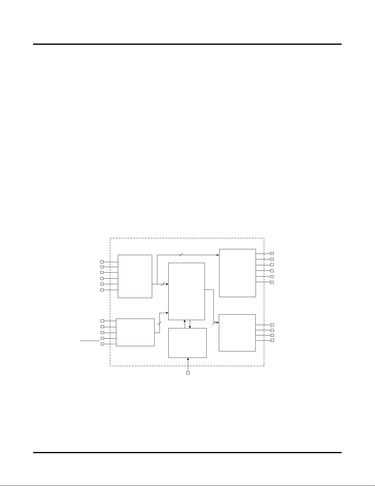
Power Supply Sequence Controller and Monitor
The ispPAC-POWR604 device is specifically designed as a fully-programmable power supply sequencing controller
and monitor for managing up to four separate power supplies, as well as monitoring up to six analog inputs or supplies. The ispPAC-POWR604 device contains an internal PLD that is programmable by the user to implement digital logic functions and control state machines. The internal PLD connects to two programmable timers, special
purpose I/O and the programmable monitoring circuit blocks. The internal PLD and timers can be clocked by either
an internal programmable clock oscillator or an external clock source.
The voltage monitors are arranged as six independent comparators each with 192 programmable trip point settings. Monitoring levels are set around the following standard voltages: 1.2V, 1.5V, 1.8V, 2.5V, 3.3V or 5.0V.
All six voltages can be monitored simultaneously (i.e., continuous-time operation). Other non-standard voltage levels can be accounted for using various scale factors.
For added robustness, the comparators feature a variable hysteresis that scales with the voltage they monitor.
Generally, a larger hysteresis is better. However, as power supply voltages get smaller, that hysteresis increasingly
affects trip-point accuracy. Therefore, the hysteresis is +/-16mV for 5V supplies and scales down to +/-3mV for 1.2V
supplies, or about 0.3% of the trip point.
The programmable logic functions consist of a block of 20 inputs with 41 product terms and eight macrocells. The
architecture supports the sharing of product terms to enhance the overall usability.
The four output pins are open-drain outputs. These outputs can be used to drive enable lines for DC/DC converters
or other control logic associated with power supply control. The four outputs are driven from the macrocells.
Figure 1. ispPAC-POWR604 Block Diagram
ispPAC-POWR604
VMON1
VMON2
VMON3
VMON4
VMON5
VMON6
IN1
IN2
IN3
IN4
RESET
Analog
Inputs
Digital
Inputs
5
6
6
Sequence
Controller
CPLD
20 I/P & 8
Macrocell
GLB
250kHz
Internal
OSC
2 Timers
Comparator
Outputs
4
Logic
Outputs
COMP1
COMP2
COMP3
COMP4
COMP5
COMP6
OUT5
OUT6
OUT7
OUT8
CLKIO
2

Lattice Semiconductor ispPAC-POWR604 Data Sheet
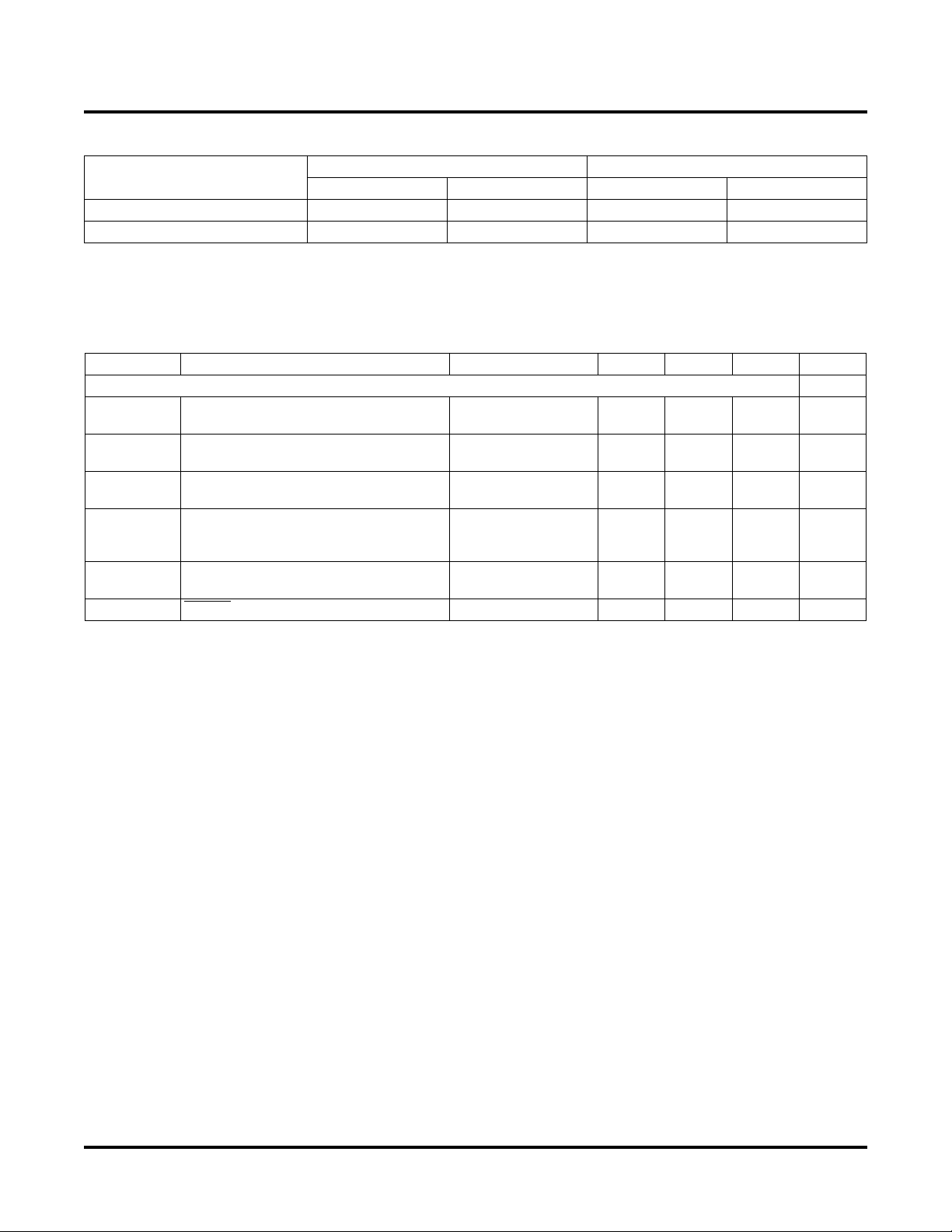
Pin Descriptions
Number Name Pin Type Voltage Range Description
1NC— — No Connect
2NC— — No Connect
3NC— — No Connect
4NC— — No Connect
5 VDD Power 2.25V-5.5V Main Power Supply
6 IN1 CMOS Input VDDINP
7 IN2 CMOS Input VDDINP
8 IN3 CMOS Input VDDINP
9 IN4 CMOS Input VDDINP
10 RESET
CMOS input VDD
11 VDDINP Power 2.25V-5.5V
12 OUT5
13 OUT6
14 OUT7
15 OUT8
8
O/D Output 2.25V-5.5V
8
O/D Output 2.25V-5.5V
8
O/D Output 2.25V-5.5V
8
O/D Output 2.25V-5.5V
1, 3
1, 3
1, 3
1, 3
6
3
2
2
2
2
16 NC — — No Connect
17 NC — — No Connect
18 COMP6 O/D Output 2.25V-5.5V
19 COMP5 O/D Output 2.25V-5.5V
20 COMP4 O/D Output 2.25V-5.5V
21 COMP3 O/D Output 2.25V-5.5V
22 COMP2 O/D Output 2.25V-5.5V
23 COMP1 O/D Output 2.25V-5.5V
2
2
2
2
2
2
24 TCK TTL/LVCMOS Input VDD Test Clock (JTAG Pin)
25 POR
26 CLK Bi-directional I/O VDD
O/D Output 2.25V-5.5V Power-On-Reset Output
2, 5
27 GND Ground Ground
28 TDO TTL/LVCMOS Output VDD Test Data Out (JTAG Pin)
29 TRST
TTL/LVCMOS Input VDD
30 TDI TTL/LVCMOS Input VDD Test Data In, 50k Ohm Pull-up (JTAG Pin)
31 TMS TTL/LVCMOS Input VDD
32 VMON1 Analog Input 0V-5.72V
33 VMON2 Analog Input 0V-5.72V
34 VMON3 Analog Input 0V-5.72V
35 VMON4 Analog Input 0V-5.72V
36 VMON5 Analog Input 0V-5.72V
37 VMON6 Analog Input 0V-5.72V
4
4
4
4
4
4
38 NC — — No Connect
39 CREF Reference 1.17V
7
40 NC — — No Connect
41 NC — — No Connect
Input 1
Input 2
Input 3
Input 4
PLD Reset Input, Active Low
Digital Inputs Power Supply
Open-Drain Output
Open-Drain Output
Open-Drain Output
Open-Drain Output
VMON6 Comparator Output (Open-Drain)
VMON5 Comparator Output (Open-Drain)
VMON4 Comparator Output (Open-Drain)
VMON3 Comparator Output (Open-Drain)
VMON2 Comparator Output (Open-Drain)
VMON1 Comparator Output (Open-Drain)
Clock Output (Open-Drain) or Clock Input
Test Reset, Active Low, 50k Ohm Internal Pull-up
(JTAG Pin, Optional Use)
Test Mode Select, 50k Ohm Internal Pull-up (JTAG
Pin)
Voltage Monitor Input 1
Voltage Monitor Input 2
Voltage Monitor Input 3
Voltage Monitor Input 4
Voltage Monitor Input 5
Voltage Monitor Input 6
Reference for Internal Use, Decoupling Capacitor
(.1uf Required, CREF to GND)
3

Lattice Semiconductor ispPAC-POWR604 Data Sheet
Pin Descriptions (Continued)
Number Name Pin Type Voltage Range Description
42 NC — — No Connect
43 NC — — No Connect
44 NC — — No Connect
1. IN1...IN4 are digital inputs to the PLD. The thresholds for these pins are referenced by the voltage on VDDINP.
2. The open-drain outputs can be powered independently of VDD and pulled up as high as +6.0V (referenced to ground). Exception, CLK pin
26 can only be pulled as high as VDD.
3. VDDINP can be chosen independent of V
4. The six VMON inputs can be biased independently of VDD. The six VMON inputs can be as high as 7.0V Max (referenced to ground).
5. CLK is the PLD clock output in master mode. It is re-routed as an input in slave mode. The clock mode is set in software during design
time. In output mode it is an open-drain type pin and requires an external pull-up resistor (pullup voltage must be
POWR604 devices can be tied together with one acting as the master, the master can use the internal clock and the slave can be clocked
by the master. The slave needs to be set up using the clock as an input.
6. RESET
7. The CREF pin requires a 0.1µF capacitor to ground, near the device pin. This reference is used internally by the device. No additional
8. The four digital outputs (pins 12-15) are named OUT5-OUT8 to match ispPAC-POWR1208 pin names and to allow easy design migration.
is an active low INPUT pin, external pull-up resistor required. When driven low it resets all internal PLD flip-flops to zero, and may
turn “ON” or “OFF” the output pins, depending on the polarity configuration of the outputs in the PLD. If a reset function is needed for the
other devices on the board, the PLD inputs and outputs can be used to generate these signals. The RESET connected to the POR pin can
be used if multiple ispPAC-POWR604 devices are cascaded together in expansion mode or if a manual reset button is needed to reset the
PLD logic to the initial state. While using the ispPAC-POWR604 in hot-swap applications it is recommended that either the RESET pin be
connected to the POR pin, or connect a capacitor to ground (such that the time constant is 10 ms with the pull-up resistor) from the RESET
pin.
external circuitry should be connected to this pin.
It applies only to the four logic inputs IN1-IN4.
DD.
). Multiple ispPAC-
≤ V
DD
Absolute Maximum Ratings
Absolute maximum ratings are shown in the table below. Stresses above those listed values may cause permanent
damage to the device. Functional operation of the device at these or any other conditions above those indicated in
the operating sections of this specification is not implied.
Symbol Parameter Conditions Min. Max. Units
VDD Core supply voltage at pin — -0.5 6.0 V
VDD
V
VMON Input voltage applied, V
V
T
T
T
1. V
2. Digital inputs are tolerant up to 5.5V, independent of the V
1
INP
2
IN
TRI
S
A
SOL
DDINP
supply voltage for the given input logic range.
Digital input supply voltage for IN1-IN4 — -0.5 6.0 V
Input voltage applied, digital inputs — -0.5 6.0 V
MON
Tr istated or open drain output, external voltage applied
≤
(CLK pin 26 pull-up
VDD).
Storage temperature — -65 150 °C
Ambient temperature with power applied — -55 125 °C
Maximum soldering temperature (10 sec. at 1/16 in.) — — 260 °C
is the supply pin that controls logic inputs IN1-IN4 only. Place 0.1µF capacitor to ground and supply the V
voltage monitor inputs — -0.5 7.0 V
— -0.5 6.0 V
pin with appropriate
DDINP
voltage.
DDINP
4
Lattice Semiconductor ispPAC-POWR604 Data Sheet
Recommended Operating Conditions
Symbol Parameter Conditions Min. Max. Units
V
DD
V
DDPROG
V
DDINP
V
IN
V
MON
1
2
3
Erase/Program
Cycles
T
APROG
T
A
1. The ispPAC-POWR604 device must be powered from 3.0V to 5.5V during programming of the E
2. V
3. Digital inputs are tolerant up to 5.5V, independent of the V
is the supply pin that controls logic inputs IN1-IN4 only. Place 0.1µF capacitor to ground and supply the V
DDINP
supply voltge for the given input logic range.
Core supply voltage at pin 2.25 5.5 V
Core supply voltage at pin During E
2
cell programming 3.0 5.5 V
Digital input supply voltage for IN1-IN4 2.25 5.5 V
Input voltage digital inputs 0 5.5 V
Voltage monitor inputs V
MON1
- V
MON6
0 6.0 V
EEPROM, programmed at
V
Ambient temperature during
programming
Ambient temperature
DDINP
= 3.0V to 5.5V
DD
-40°C to +85°C
Power applied - Industrial -40 +85 °C
Power applied - Automotive -40 +125 °C
2
CMOS memory.
voltage.
1000 — Cycles
-40 +85 °C
pin with appropriate
DDINP
Analog Specifications
Over Recommended Operating Conditions
Symbol Parameter Conditions Min. Typ. Max. Units
I
DD
Supply Current Internal Clock = 250kHz — 5 10 mA
Reference
Symbol Parameter Conditions Min. Typ. Max. Units
1
V
REF
1. CREF pin requires a 0.1µF capacitor to ground.
Reference voltage at CREF pin T = 25°C — 1.17 — V
Voltage Monitors
Symbol Parameter Conditions Min. Typ. Max. Units
R
IN
V
Range Programmable voltage monitor trip
MON
V
Accuracy Absolute accuracy of any trip point T = 25 °C,
MON
V
Tempco
MON
HYST Hysteresis of V
PSR Trip point sensitivity to V
1. See typical performance curves.
Input impedance 70 100 130 k
point (192 steps)
V
= 3.3V
1
Temperature drift of any trip point -40°C to +85°C 50 ppm/ °C
DD
1.03 5.72 V
-0.9 +0.9 %
-40°C to +125°C 76 ppm/ °C
V
HYST
= HYST*V
MON
input,
(+/-3 to +/-13mV)
MON
DD
V
= 3.3V, 25°C +/- 0.3% of
DD
trip point
setting
V
= 3.3V 0.06 %/V
DD
Ω
%
5
Lattice Semiconductor ispPAC-POWR604 Data Sheet
Power-on-Reset
Symbol Parameter Conditions Min. Typ. Max. Units
V
supply threshold beyond which POR
V
LPOR
V
HPOR
1. POR tests run with 10k
DD
output is guaranteed to be driven low
V
supply threshold above which POR
DD
output is guaranteed driven high, and device
initializes
Ω resistor pulled up to V
DD.
V
ramping up
DD
ramping up
V
DD
1
1
——1.15 V
——2.1 V
AC/Transient Characteristics
Over Recommended Operating Conditions
Symbol Parameter Conditions Min. Typ. Max. Units.
Voltage Monitors
t
PD5
t
PD20
Propagation Delay. Output
transitions after a step input.
Propagation Delay. Output
transitions after a step input.
Oscillators
f
CLK
PLDCLK
Range
Internal master clock frequency Note 2 230 — 330 kHz
Programmable frequency range
of PLD clock (8 binary steps)
PLDCLKext Max frequency of applied
external clock source
Timers
Timeout
Range
1. See Typical Performance Graphs.
2. f
frequency deviation with respect to VDD, 0.4%/volt, typical.
CLK
Range of programmable
time-out duration (15 steps)
Glitch filter set to 5µs.
Input V
+ 100mV to V
TRIP
Glitch filter set to 20us.
Input V
+ 100mV to V
TRIP
Internal Osc 250kHz
External clock applied
Internal Osc 250kHz
1
1
TRIP
TRIP
- 100mV
- 100mV
—5—µs
—20—µs
1.95 — 250 kHz
—— 1MHz
0.03 — 524 ms
Digital Specifications
Over Recommended Operating Conditions
Symbol Parameter Conditions Min. Typ. Max. Units
≤
V
≤
I
I
IL,
IH
I
PU
V
OL
I
SINKOUT
Input or I/O leakage current, no pull-up0V
25 °C
Input pull-up current (TMS, TDI,
TRST
)
Open-drain output set LOW I
Maximum sink current for logic out-
25 °C 70 µA
SINKOUT
(Note 1)
puts [OUT5-OUT8], [COMP1COMP6]
I
SINKTOTAL
1. [OUT5-OUT8] and [COMP1-COMP6] can sink up to 20mA max. per pin for LEDs, etc. However, output voltage levels may exceed VOL. Total
combined sink currents from all outputs (OUT, COMP) should not exceed I
Total combined sink currents from all
outputs [OUT, COMP]
(Note 1)
V
IN
DDINP
or V
DD
+/-10 µA
= 4mA 0.4 V
20 mA
80 mA
SINKTOTAL
.
6
Lattice Semiconductor ispPAC-POWR604 Data Sheet
DC Input Levels: IN1-IN4
VIL (V) VIH (V)
Standard
Min. Max. Min. Max.
CMOS, LVCMOS3.3, LVTTL, TTL -0.3 0.8 2.0 5.5
LVCMOS2.5 -0.3 0.7 1.7 5.5
Note: V
V
DDINP.
is the input supply pin for IN1-IN4 digital logic input pins. The logic threshold trip point of IN1-IN4 is dependent on the voltage at
DDINP
Transient Characteristics
Over Recommended Operating Conditions
Symbol Parameter Conditions Min. Typ. Max. Units
PLD Timing
Digital Glitch
Filter
t
CO
t
SU
t
H
t
PD
t
RST
1. External clock 1MHz. Open drain outputs with 2k pull-up resistor to VDD.
Note: All the above parameters apply to signal paths from the digital inputs [IN1-IN4].
Minimum pulse width to transition through
glitch filter.
Clock to Out Delay. Rising edge of clock to
output transition.
Time that input needs to be present when
using a registered function with the clock.
Time that input needs to be held valid after
the clock edge when using a registered
Applied to IN1-IN4
Stable input before
clock edge (Note 1)
Data valid before clock
(Note 1)
Hold data after clock
20 µs
300 ns
20 µs
0 µs
function with the clock.
Propagation delay internal to the
embedded PLD
90 ns
RESET pulse width 25 µs
7
Lattice Semiconductor ispPAC-POWR604 Data Sheet
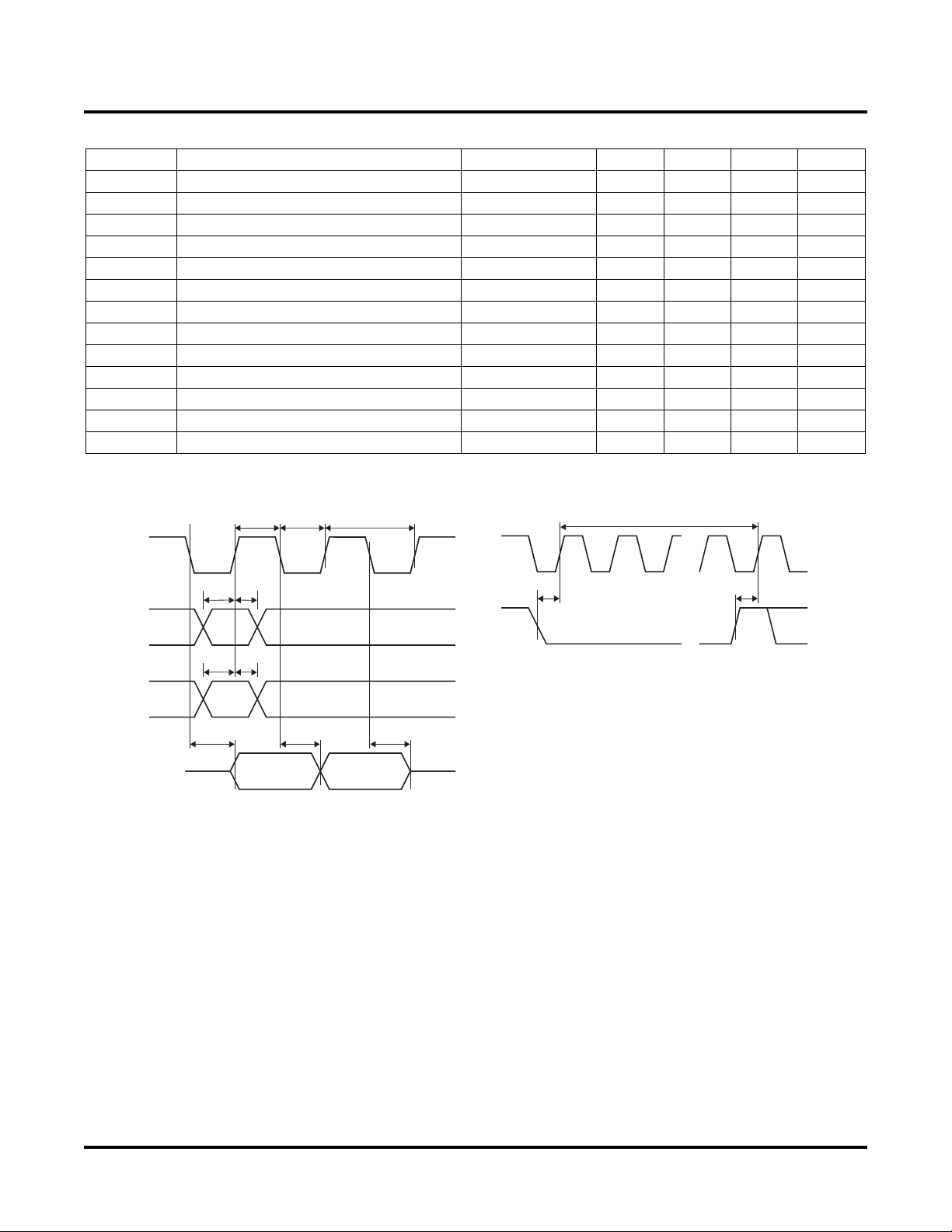
Timing for JTAG Operations
Symbol Parameter Conditions Min Typ. Max Units
t
CKMIN
t
CKH
t
CKL
t
MSS
t
MSH
t
DIS
t
DIH
t
DOZX
t
DOV
t
DOXZ
t
RSTMIN
t
PWP
t
PWE
1. t
represents programming pulse width for a single row of E2CMOS cells.
PWP
Minimum clock period 1 µs
TCK high time 200 ns
TCK low time 200 ns
TMS setup time 15 ns
TMS hold time 50 ns
TDI setup time 15 ns
TDI hold time 50 ns
TDO float to valid delay 200 ns
TDO valid delay 200 ns
TDO valid to float delay 200 ns
Minimum reset pulse width 40 ns
Time for a programming operation
1
40 100 ms
Time for an erase operation 40 100 ms
t
t
CKH
CKL
t
CK
t
MSS
MSH
t
MS
t
DIStDIH
t
DI
t
DOZH
t
DO
t
DOV
t
CKMIN
t
DOXZ
t
CK
t
MSS
t
MS
Program and Erase cycles
executed in Run-Test/Idle
t
PWP, tPWE
t
MSSt
8
Lattice Semiconductor ispPAC-POWR604 Data Sheet
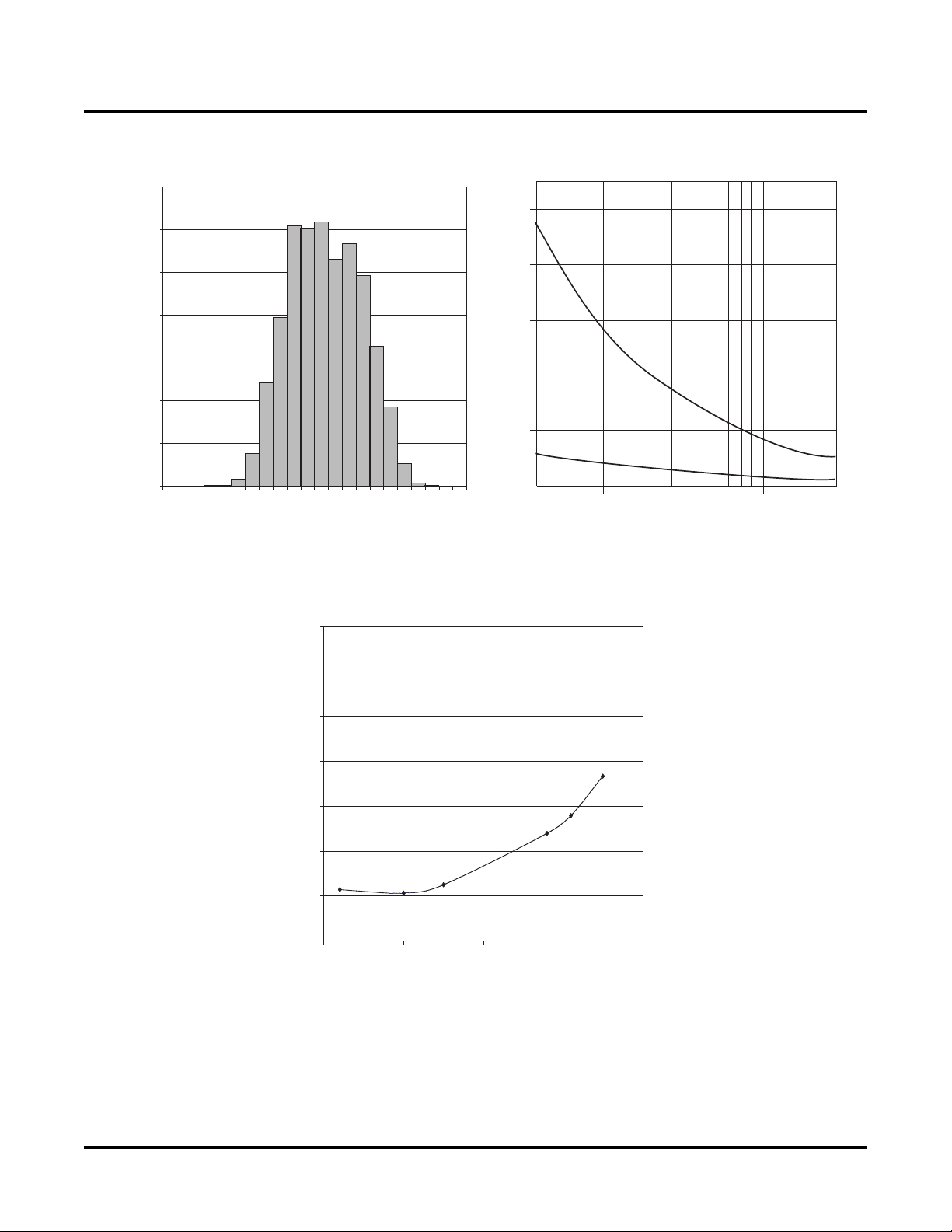
Typical Performance Graphs
7000
6000
5000
4000
Count
3000
2000
1000
0
Trip Point Error 25°C
MON
3
Typical V
Accuracy vs. Temperature
Comparator Trip Point
MON
Propagation Delay vs. OverdriveV
125
100
Glitch Filter = 20µs
75
50
Propagation Delay (µs)
25
Glitch Filter = 5µs
0
10-1 -0.8 -0.6 -0.4 -0.2 0 10.2 0.4 0.6 0.8 20 50 100 200
Input Overdrive (mV)Trip Point Error %
Note: Typical propagation delay of V
as a function of overdrive beyond selected trip point.
inputs to outputs
MON
2.5
2
1.5
% Error
1
0.5
0
-0.5
-50 0 50 100 150
Temperature (°C)
9

Lattice Semiconductor ispPAC-POWR604 Data Sheet
Table 1. V
1.2 low 1.2 high 1.5 low 1.5 high 1.8 low 1.8 high 2.5 low 2.5 high 3.3 low 3.3 high 5.0 low 5.0 high
1.036 1.202 1.291 1.502 1.549 1.801 2.153 2.500 2.842 3.297 4.299 4.991
1.046 1.213 1.303 1.516 1.564 1.818 2.173 2.524 2.869 3.328 4.340 5.038
1.056 1.225 1.316 1.531 1.579 1.836 2.195 2.549 2.897 3.361 4.383 5.088
1.066 1.237 1.329 1.546 1.595 1.854 2.216 2.574 2.926 3.394 4.426 5.138
1.076 1.249 1.341 1.560 1.609 1.871 2.237 2.597 2.952 3.425 4.466 5.185
1.087 1.261 1.354 1.575 1.625 1.889 2.258 2.622 2.981 3.458 4.509 5.235
1.096 1.272 1.366 1.590 1.639 1.906 2.279 2.646 3.008 3.489 4.550 5.282
1.107 1.284 1.379 1.605 1.655 1.924 2.300 2.671 3.036 3.522 4.593 5.332
1.117 1.295 1.391 1.619 1.669 1.941 2.320 2.694 3.063 3.553 4.633 5.379
1.127 1.307 1.404 1.634 1.685 1.959 2.342 2.719 3.091 3.586 4.676 5.429
1.137 1.319 1.417 1.649 1.700 1.977 2.363 2.744 3.120 3.619 4.719 5.479
1.147 1.331 1.429 1.663 1.715 1.994 2.384 2.768 3.147 3.650 4.760 5.526
1.157 1.343 1.442 1.678 1.730 2.012 2.405 2.793 3.175 3.683 4.803 5.576
1.168 1.355 1.455 1.693 1.746 2.030 2.427 2.818 3.203 3.716 4.846 5.626
1.178 1.366 1.467 1.707 1.761 2.047 2.447 2.841 3.230 3.747 4.886 5.673
1.188 1.378 1.480 1.722 1.776 2.065 2.469 2.866 3.259 3.780 4.929 5.723
1.All possible comparator trip voltages using internal attenuation settings.
Trip Point Table
MON
1
Ta ble 1 shows all possible comparator trip point voltage settings. The internal resistive divider allows ranges for
1.2V, 1.8V, 2.5V, 3.3V and 5.0V. There are 192 available voltages, ranging from 1.036V to 5.723V. In addition to the
192 voltage monitor trip points, the user can add additional resistors outside the device to divide down the voltage
and achieve virtually any voltage trip point. This allows the capability to monitor higher voltages such and 12V, 15V,
24V, etc. Voltage monitor trip points are set in the graphical user interface of the PAC-Designer software by simple
pull-down menus. The user simply selects the given range and corresponding trip point value. Attenuation and reference values are set internally using E2CMOS configuration bits internal to the device.
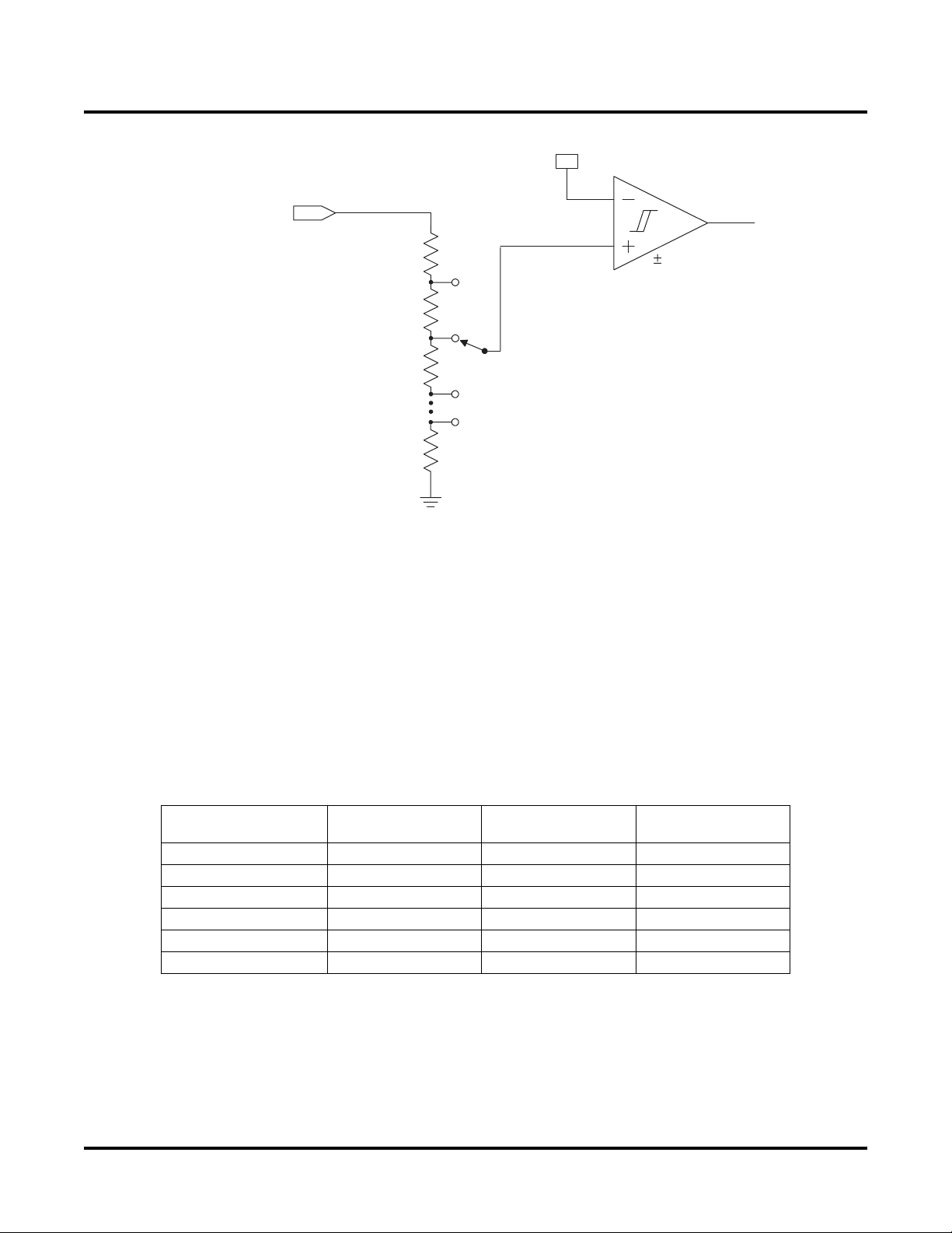
Figure 2 shows a single comparator, the attenuation network and reference used to program the monitor trip points.
Each of the six comparators are independently set in the same way.
Theory Of Operation
The ispPAC-POWR604 incorporates programmable voltage monitors along with digital inputs and outputs. The
eight macrocell PLD inputs are from the six voltage monitors and four digital inputs. There are two embedded programmable timers that interface with the PLD, along with an internal programmable oscillator.
The six independently programmable voltage monitors each have 192 programmable trip points.
Figure 2 shows a simplified schematic representation of one of these monitors.
10
Lattice Semiconductor ispPAC-POWR604 Data Sheet
Figure 2. Voltage Monitors
Reference
Monitor Voltage
VMON1..VMON6
To PLD Array
3mV
Hysteresis
Each monitor consists of three major subsystems. The core of the monitor is a voltage comparator. This comparator outputs a HIGH signal to the PLD array if the voltage at its positive terminal is greater than that at its negative
terminal, otherwise it outputs a LOW signal. A small amount of hysteresis is provided by the comparator to reduce
the effects of input noise.
The input signal is attenuated by a programmable resistive divider before it is fed into the comparator. This feature
is used to determine the coarse range in which the comparator should trip (e.g. 1.8V, 3.3V, 5V). Twelve possible
ranges are available from the input divider network. The comparator’s negative terminal is obtained from a programmable reference source (Reference), which may be set to one of 16 possible values scaled in approximately
1% increments from each other, allowing for fine tuning of the voltage monitor’s trip points. This combination of
coarse and fine adjustment supports 192 possible trip-point voltages for a given monitor circuit. Because each
monitor’s reference and input divider settings are completely independent of those of the other monitor circuits, the
user can set any input monitor to any of the 192 available settings.
Comparator Hysteresis
V
MON
Range Setting
5.0V +/- 16.2 +/- 14.0 mV
3.3V +/- 10.7 +/- 9.2 mV
2.5V +/- 8.1 +/- 7.0 mV
1.8V +/- 5.8 +/- 5.0 mV
1.5V +/- 4.9 +/- 4.2 mV
1.2V +/- 3.9 +/- 3.4 mV
1. The hysteresis scales depending on the voltage monitor range that is selected. The values show are typical and
are centered around the nominal voltage trip point for a given range selection.
Typical Hysteresis on
1
Over Voltage Range
Typical Hysteresis on
Under Voltage Range Units
PLD Architecture
The ispPAC-POWR604 digital logic is composed of an internal PLD that is programmed to perform the sequencing
functions. The PLD architecture allows flexibility in designing various state machines and control logic used for
monitoring. The macrocell shown in Figure 3 is the heart of the PLD. There are eight macrocells that can be used to
11

Lattice Semiconductor ispPAC-POWR604 Data Sheet
control the functional states of the sequencer state machine or other control or monitoring logic. The PLD AND
array shown in Figure 4 has 20 inputs and 41 product terms (PTs). The resources from the AND array feed the
eight macrocells. The resources within the macrocells share routing and contain a product-term allocation array.
The product term allocation array greatly expands the PLD’s ability to implement complex logical functions by
allowing logic to be shared between adjacent blocks and distributing the product terms to allow for wider decode
functions.
The basic macrocell has five product terms that feed the OR gate and the flip-flop. The flip-flop in each macrocell is
independently configured. It can be programmed to function as a D-Type or T-Type flip-flop. The combinatorial functions are achieved through the bypass MUX function shown. By having the polarity control XOR, the logic reduction
can be best fit to minimize the number of product terms. The flip-flop’s clock drives from a common clock that can
be generated from a pre-scaled, on-board clock source or from an external clock. The macrocell also supports
asynchronous reset and preset functions, derived from product terms, the global reset input, or the power-on reset
signal.
Figure 3. ispPAC-POWR604 Macrocell Block Diagram
Global Reset Power On Reset
Global Polarity Fuse for
Block Init Product-Term
Init Product-Term
PT4
PT3
PT2
PT1
PT0
Clock
Polarity
Product-Term Allocation
R
P
D/T Q
CLK
Macrocell Flip-Flop provides
D,T or Combinatorial
Output with Polarity
To ORP
12

Lattice Semiconductor ispPAC-POWR604 Data Sheet
Figure 4. PLD and Timer Functional Block Diagram
POR/RESET
MC0
VMON[1:6]
Comparators
IN[1:4]
MC1
MC2
AND
ARRAY
6
20 Inputs
41 PT
8 Outputs
4
MC3
MC4
MC5
MC6
MC7
Output
Routing
Pool
OUT5
OUT6
OUT7
OUT8
2
8
Timer1
BLK-INIT PT
8
Timer2
Routing
Pool
Clock Generation
13

Lattice Semiconductor ispPAC-POWR604 Data Sheet
Clock and Timer Systems
Figure 5 shows a block diagram of the ispPAC-POWR604’s internal clock and timer systems. The PLD clock can be
programmed with eight different frequencies based on the internal oscillator frequency of 250kHz.
Figure 5. Clock and Timer Block
Internal
OSC
250kHz
CLK
Table 2. PLD Clock Prescaler
PLD Clock Frequency (kHz) PLD Prescaler Divider
1. Values based on 250kHz clock.
Timer1
Timer Prescaler
(Time Out Range)
Timer2
PLD Clock
Prescaler
1
250 1
125 2
62.5 4
31.3 8
15.6 16
7.8 32
3.9 64
2 128
The internal oscillator runs at a fixed frequency of 250kHz. This main signal is then fed to the PLD clock pre-scaler
and also the Timer Clock pre-scaler (Figure 5). For the PLD Clock, the main 250kHz oscillator is divided down to
eight selectable frequencies shown in the Table 2. The architecture of the clock network allows the PLD clock to be
driven to the CLK pin. This enables the user access to the PLD clock as an output for expansion mode or other
uses of the (CLK) clock pin.
Schematically, when the switch is in the upper position, the internal oscillator drives the PLD clock pre-scaler and
the timer pre-scaler. In this mode, the CLK pin is an open-drain output and represents the same frequency as the
PLD clock. This is used when operating other devices (such as “slave” sequencing devices) in a synchronized
mode. When the switch is in the lower position, the CLK pin is an input and must be driven with an external clock
source. When driven from an external source, the same PLD clock pre-scaler is available to this external clock. The
frequencies available for the PLD clock will be the external clock frequency divided by 1, 2, 4, 8, 16, 32, 64 or 128,
depending on the programmable value chosen.
The Timer Clock Pre-Scaler divides the internal 250kHz oscillator (or external clock, if selected) down before it generates the clock for the two programmable timers. The pre-scaler has eight different divider ratios: Divide by 4, 8,
16, 32, 64, 128, 256 and 512 (Table 3). After the clock for the timers is divided down, it is used to drive the programmable timers. The two timers share the same timer clock frequency but may have different end count values. The
14

Lattice Semiconductor ispPAC-POWR604 Data Sheet
timers can cover a range from 32us to 524ms for the internal oscillator. Longer delays can be achieved by using the
external clock as an input.
Table 3. Timer Values
1
÷÷÷÷ 4
62 kHz
÷÷÷÷ 8
31.2 kHz
÷÷÷÷ 16
15.6 kHz
÷÷÷÷ 32
7.8 kHz
÷÷÷÷ 64
3.9 kHz
÷÷÷÷ 128
2 kHz
÷÷÷÷ 256
1 kHz
÷÷÷÷ 512
0.5 kHz
0.032 ms
0.064 ms 0.064 ms
0.128 ms 0.128 ms 0.128 ms
0.256 ms 0.256 ms 0.256 ms 0.256 ms
0.512 ms 0.512 ms 0.512 ms 0.512 ms 0.512 ms
1.024 ms 1.024 ms 1.024 ms 1.024 ms 1.024 ms 1.024 ms
2.048 ms 2.048ms 2.048ms 2.048ms 2.048ms 2.048ms 2.048ms
4.096 ms 4.096 ms 4.096 ms 4.096 ms 4.096 ms 4.096 ms 4.096 ms 4.096 ms
8.192 ms 8.192 ms 8.192 ms 8.192 ms 8.192 ms 8.192 ms 8.192 ms
16.384 ms 16.384 ms 16.384 ms 16.384 ms 16.384 ms 16.384 ms
32.768 ms 32.768 ms 32.768 ms 32.768 ms 32.768 ms
65.536 ms 65.536 ms 65.536 ms 65.536 ms
131.072 ms 131.072 ms 131.072 ms
262.144 ms 262.144 ms
524.288 ms
1. Timer values based on 250kHz clock.
For design entry, the user can select the source for the clock and the PAC-Designer software will calculate the
appropriate delays in an easy-to-select menu format.
The control inputs for Timer1 and Timer2 can be driven by any of the eight PLD macrocell outputs. The reset for the
timers is a function of the Global Reset pin (RESET), a power-on reset or when the timer input goes low. The waveforms in Figure 6 show the basic timer start and reset functions. Timer and clock divider values are specified in during the design phase using the PAC-Designer software, while simple pull-down menus allow the user to select the
clocking mode and the values for the timers and the PLD clock.
Figure 6. Timer Waveforms
Timer Gate
(From PLD)
Timer Output
(To PLD)
Start
Timer
ProgrammableTimer
Timer Period
Delay
Timer
Expired
Reset
Timer
Start
Timer
Timer Period
Timer
Expired
ProgrammableTimer
Delay
Note that if the clock module is configured as “slave” (i.e. the CLK is an input), the actual time-out of the two timers
is determined by the external clock frequency.
15

Lattice Semiconductor ispPAC-POWR604 Data Sheet
IEEE Standard 1149.1 Interface
In-system programming of the ispPAC-POWR604 is facilitated via an IEEE 1149.1 test access port (TAP). It is used
by the ispPAC-POWR604 as a serial programming interface, boundary scan test is not supported. There are no
boundary scan logic registers in the ispPAC-POWR604 architecture. This does not prevent the ispPAC-POWR604
from functioning correctly, however, when placed in a valid serial chain with other IEEE 1149.1 compliant devices.
Since the ispPAC-POWR604 is used to powerup other devices, it should be programmed in a separate chain from
PLDs, FPGAs or other JTAG devices.
A brief description of the ispPAC-POWR604 serial interface follows. For complete details of the reference specifica-
tion, refer to the publication, Standard Test Access Port and Boundary-Scan Architecture, IEEE Std 1149.1-1990
(which now includes IEEE Std 1149.1a-1993).
Overview
An IEEE 1149.1 test access port (TAP) provides the control interface for serially accessing the digital I/O of the ispPAC-POWR604. The TAP controller is a state machine driven with mode and clock inputs. Instructions are shifted
into an instruction register, which then determines subsequent data input, data output, and related operations.
Device programming is performed by addressing various registers, shifting data in, and then executing the respective program instruction. The programming instructions transfer the data into internal E2CMOS memory. It is these
non-volatile memory cells that determine the configuration of the ispPAC-POWR604. By cycling the TAP controller
through the necessary states, data can also be shifted out of the various registers to verify the current ispPACPOWR604 configuration. Instructions exist to access all data registers and perform internal control operations.
For compatibility between compliant devices, two data registers are mandated by the IEEE 1149.1 specification.
Other registers are functionally specified, but inclusion is strictly optional. Finally, there are provisions for optional
user data registers that are defined by the manufacturer. The two required registers are the bypass and boundaryscan registers. For ispPAC-POWR604, the bypass register is a 1-bit shift register that provides a short path through
the device when boundary testing or other operations are not being performed. The ispPAC-POWR604, as mentioned earlier has no boundary-scan logic and therefore no boundary scan register. All instructions relating to
boundary scan operations place the ispPAC-POWR604 in the BYPASS mode to maintain compliance with the
specification.
The optional identification (IDCODE) register described in IEEE 1149.1 is also included in the ispPAC-POWR604.
Six additional user data registers are included in the TAP of the ispPAC-POWR604 as shown in Figure 7. Most of
these additional registers are used to program and verify the analog configuration (CFG) and PLD bits. A status
register is also provided to read the status of the six analog comparators.
16

Lattice Semiconductor ispPAC-POWR604 Data Sheet
Figure 7. TAP Registers
ANALOG COMPARATOR ARRAY (6 bits)
STATUS REGISTER (6 bits)
IDCODE REGISTER (32 bits)
UES REGISTER (16 bits)
MULTIPLEXER
CFG REGISTER (17 bits)
CFG ADDRESS REGISTER (4 bits)
PLD DATA REGISTER (41 bits)
PLD ADDRESS REGISTER (43 bits)
INSTRUCTION REGISTER (6 bits)
BYPASS REGISTER (1 bit)
TEST ACCESS PORT
(TAP) LOGIC
OUTPUT
LATCH
ANALOG
CONFIGURATION
2
E
NON-VOLATILE
MEMORY
(68 bits)
PLD
AND / ARCH
2
NON-VOLATILE
E
MEMORY
(1763 bits)
TDI TCK TMS TDO
TAP Controller Specifics
The TAP is controlled by the Test Clock (TCK) and Test Mode Select (TMS) inputs. These inputs determine whether
an Instruction Register or Data Register operation is performed. Driven by the TCK input, the TAP consists of a
small 16-state controller. In a given state, the controller responds according to the level on the TMS input as shown
in Figure 8. Test Data In (TDI) and TMS are latched on the rising edge of TCK, with Test Data Out (TDO) becoming
valid on the falling edge of TCK. There are six steady states within the controller: Test-Logic-Reset, Run-Test/Idle,
Shift-Data-Register, Pause-Data-Register, Shift-Instruction-Register, and Pause-Instruction-Register. But there is
only one steady state for the condition when TMS is set high: the Test-Logic-Reset state. This allows a reset of the
test logic within five TCKs or less by keeping the TMS input high. Test-Logic-Reset is the power-on default state.
When the correct logic sequence is applied to the TMS and TCK inputs, the TAP will exit the Test-Logic-Reset state
and move to the desired state. The next state after Test-Logic-Reset is Run-Test/Idle. Until a data or instruction
scan is performed, no action will occur in Run-Test/Idle (steady state = idle). After Run-Test/Idle, either a data or
instruction scan is performed. The states of the Data and Instruction Register blocks are identical to each other differing only in their entry points. When either block is entered, the first action is a capture operation. For the Data
Registers, the Capture-DR state is very simple; it captures (parallel loads) data onto the selected serial data path
(previously chosen with the appropriate instruction). For the Instruction Register, the Capture-IR state will always
load the IDCODE instruction. It will always enable the ID Register for readout if no other instruction is loaded prior
17

Lattice Semiconductor ispPAC-POWR604 Data Sheet
to a Shift-DR operation. This, in conjunction with mandated bit codes, allows a “blind” interrogation of any device in
a compliant IEEE 1149.1 serial chain.
Figure 8. TAP States
Test-Logic-Reset
1
0
Run-Test/Idle
0
Select-DR-Scan
1
0
Capture-DR
0
Shift-DR
1
Exit1-DR
0
Select-IR-Scan
1
0
1
0
Capture-IR
0
Shift-IR
1
Exit1-IR
0
111
0
1
0
Pause-IR
1
Exit2-IR
1
Update-IR
0
0101
Pause-DR
1
0
Exit2-DR
1
Update-DR
Note: The value shown adjacent to each state transition represents the signal present
at TMS at the time of a rising edge at TCK.
0
From the Capture state, the TAP transitions to either the Shift or Exit1 state. Normally the Shift state follows the
Capture state so that test data or status information can be shifted out or new data shifted in. Following the Shift
state, the TAP either returns to the Run-Test/Idle state via the Exit1 and Update states or enters the Pause state via
Exit1. The Pause state is used to temporarily suspend the shifting of data through either the Data or Instruction
Register while an external operation is performed. From the Pause state, shifting can resume by re-entering the
Shift state via the Exit2 state or be terminated by entering the Run-Test/Idle state via the Exit2 and Update states.
If the proper instruction is shifted in during a Shift-IR operation, the next entry into Run-Test/Idle initiates the test
mode (steady state = test). This is when the device is actually programmed, erased or verified. All other instructions
are executed in the Update state.
Test Instructions
Like data registers, the IEEE 1149.1 standard also mandates the inclusion of certain instructions. It outlines the
function of three required and six optional instructions. Any additional instructions are left exclusively for the manufacturer to determine. The instruction word length is not mandated other than to be a minimum of two bits, with only
the BYPASS and EXTEST instruction code patterns being specifically called out (all ones and all zeroes respectively). The ispPAC-POWR604 contains the required minimum instruction set as well as one from the optional
instruction set. In addition, there are several proprietary instructions that allow the device to be configured, verified,
and monitored. For ispPAC-POWR604, the instruction word length is 6-bits. All ispPAC-POWR604 instructions
available to users are shown in Table 4.
18

Lattice Semiconductor ispPAC-POWR604 Data Sheet
Table 4. ispPAC-POWR604 TAP Instruction Table
Instruction Code Description
EXTEST 000000 External Test. Defaults to BYPASS.
ADDPLD
DATAPLD
ERASEAND
ERASEARCH
PROGPLD
PROGESF
1
1
1, 2
1, 2
1, 2
1, 2
BYPASS 000111 Bypass (connect TDI to TDO).
READPLD
DISCHARGE
ADDCFG
DATAC F G
ERASECFG
PROGCFG
READCFG
CFGBE
SAFESTATE
PROGRAMEN
1
1
1
1
1, 2
1, 2
1
1, 2
1
1
IDCODE 011001 Address Identification Code data register (32 bits).
PROGRAMDIS 011010 Disable Program mode (normal IO)
ADDSTATUS 011011 Address STATUS register (6 bits).
SAMPLE 011100 Sample/Preload. Default to Bypass.
ERASEUES
1, 2
SHIFTUES 011110 Reads UES data from E
PROGUES
1, 2
BYPASS 1xxxxx Bypass (connect TDI to TDO).
1. When these instructions are executed, the outputs are placed in the same mode as the instruction SAFESTATE (as
described later) to prevent invalid and potentially destructive power supply sequencing.
2. Instructions that erase or program the E2CMOS memory must be executed only when the supply to the device is
maintained at 3.0V to 5.5V.
000001 Address PLD address register (43 bits).
000010 Address PLD column data register (81 bits).
000011 Bulk Erase AND array.
000100 Bulk Erase Architect array.
000101 Program PLD column data register into E2.
000110 Program the Electronic Security Fuse bit.
001000 Reads PLD column data from E2 to the register (81 bits).
001001 Fast VPP discharge.
001010 Address CFG array address (4 bits).
001011 Address CFG data (41 bits).
001100 Bulk Erase CFG data.
001101 Program CFG data register into E2.
001110 Read CFG column data from E2 to the register (41 bits).
010110 Bulk Erase all E2 memory (CFG, PLD, USE, and ESF).
010111 Digital outputs hiZ (FET pulled L)
011000 Enable program mode (SAFESTATE IO)
011101 Bulk Erase UES.
2
and selects the UES register (16 bits).
011111 Program UES data register into E2.
BYPASS is one of the three required instructions. It selects the Bypass Register to be connected between TDI and
TDO and allows serial data to be transferred through the device without affecting the operation of the ispPACPOWR604. The IEEE 1149.1 standard defines the bit code of this instruction to be all ones (111111).
The required SAMPLE/PRELOAD instruction dictates the Boundary-Scan Register be connected between TDI
and TDO. The ispPAC-POWR604 has no boundary scan register, so for compatibility it defaults to the BYPASS
mode whenever this instruction is received. The bit code for this instruction is defined by Lattice as shown in
Ta ble 4.
The EXTEST (external test) instruction is required and would normally place the device into an external boundary
test mode while also enabling the boundary scan register to be connected between TDI and TDO. Again, since the
ispPAC-POWR604 has no boundary scan logic, the device is put in the BYPASS mode to ensure specification compatibility. The bit code of this instruction is defined by the 1149.1 standard to be all zeros (000000).
The optional IDCODE (identification code) instruction is incorporated in the ispPAC-POWR604 and leaves it in its
functional mode when executed. It selects the Device Identification Register to be connected between TDI and
TDO. The Identification Register is a 32-bit shift register containing information regarding the IC manufacturer,
19

Lattice Semiconductor ispPAC-POWR604 Data Sheet
device type and version code (Figure 9). Access to the Identification Register is immediately available, via a TAP
data scan operation, after power-up of the device, or by issuing a Test-Logic-Reset instruction. The bit code for this
instruction is defined by Lattice as shown in Table 4.
Figure 9. ID Code
MSB LSB
XXXX / 0000 0001 0100 0001 / 0000 0100 001 / 1
Part Number
0141h = ispPAC-POWR604
Version
(4 bits)
2
E
Configured
(16 bits)
JEDEC Manufacturer
Identity Code for
Lattice Semiconductor
(11 bits)
per 1149.1-1990
Constant 1
(1 bit)
ispPAC-POWR604 Specific Instructions
There are 21 unique instructions specified by Lattice for the ispPAC-PWR604. These instructions are primarily
used to interface to the various user registers and the E2CMOS non-volatile memory. Additional instructions are
used to control or monitor other features of the device. A brief description of each unique instruction is provided in
detail below, and the bit codes are found in Table 4.
ADDPLD – This instruction is used to set the address of the PLD AND/ARCH arrays for subsequent program or
read operations. This instruction also forces the outputs into the SAFESTATE.
DATAPLD – This instruction is used to shift PLD data into the register prior to programming or reading. This
instruction also forces the outputs into the SAFESTATE.
ERASEAND – This instruction will bulk erase the PLD AND array. The action occurs at the second rising edge of
TCK in Run-Test-Idle JTAG state. The device must already be in programming mode PROGRAMEN instruction).
This instruction also forces the outputs into the SAFESTATE.
ERASEARCH – This instruction will bulk erase the PLD ARCH array. The action occurs at the second rising edge
of TCK in Run-Test-Idle JTAG state. The device must already be in programming mode (PROGRAMEN instruction).
This instruction also forces the outputs into the SAFESTATE.
PROGPLD – This instruction programs the selected PLD AND/ARCH array column. The specific column is prese-
lected by using ADDPLD instruction. The programming occurs at the second rising edge of the TCK in Run-TestIdle JTAG state. The device must already be in programming mode (PROGRAMEN instruction) and operated at
3.3V to 5.0V. This instruction also forces the outputs into the SAFESTATE.
PROGESF – This instruction is used to program the electronic security fuse (ESF) bit. Programming the ESF bit
protects proprietary designs from being read out. The programming occurs at the second rising edge of the TCK in
Run-Test-Idle JTAG state. The device must already be in programming mode (PROGRAMEN instruction). This
instruction also forces the outputs into the SAFESTATE.
READPLD – This instruction is used to read the content of the selected PLD AND/ARCH array column. This specific column is preselected by using ADDPLD instruction. This instruction also forces the outputs into the SAFESTATE.
DISCHARGE – This instruction is used to discharge the internal programming supply voltage after an erase or programming cycle and prepares ispPAC-POWR604 for a read cycle. This instruction also forces the outputs into the
SAFESTATE.
20

Lattice Semiconductor ispPAC-POWR604 Data Sheet
ADDCFG – This instruction is used to set the address of the CFG array for subsequent program or read operations.
This instruction also forces the outputs into the SAFESTATE.
DATACFG – This instruction is used to shift data into the CFG register prior to programming or reading. This
instruction also forces the outputs into the SAFESTATE.
ERASECFG – This instruction will bulk erase the CFG array. The action occurs at the second rising edge of TCK in
Run-Test-Idle JTAG state. The device must already be in programming mode (PROGRAMEN instruction). This
instruction also forces the outputs into the SAFESTATE.
PROGCFG – This instruction programs the selected CFG array column. This specific column is preselected by
using ADDCFG instruction. The programming occurs at the second rising edge of the TCK in Run-Test-Idle JTAG
state. The device must already be in programming mode (PROGRAMEN instruction). This instruction also forces
the outputs into the SAFESTATE.
READCFG – This instruction is used to read the content of the selected CFG array column. This specific column is
preselected by using ADDCFG instruction. This instruction also forces the outputs into the SAFESTATE.
CFGBE – This instruction will bulk erase all E2CMOS bits (CFG, PLD, UES, and ESF) in the ispPAC-POWR604.
The device must already be in programming mode (PROGRAMEN instruction). This instruction also forces the outputs into the SAFESTATE.
SAFESTATE – This instruction turns off all of the open-drain output transistors. Pins that are programmed as FET
drivers will be placed in the active low state. This instruction is effective after Update-Instruction-Register JTAG
state.
PROGRAMEN – This instruction enables the programming mode of the ispPAC-POWR604. This instruction also
forces the outputs into the SAFESTATE.
IDCODE – This instruction connects the output of the Identification Code Data Shift (IDCODE) Register to TDO
(Figure 10), to support reading out the identification code.
Figure 10. IDCODE Register
Bit
31
Bit
30
Bit
29
Bit
28
Bit
27
Bit
Bit
4
3
Bit
2
Bit
1
Bit
TDO
0
PROGRAMDIS – This instruction disables the programming mode of the ispPAC-POWR604. The Test-Logic-Reset
JTAG state can also be used to cancel the programming mode of the ispPAC-POWR604.
ADDSTATUS – This instruction is used to both connect the status register to TDO (Figure 11) and latch the 6 voltage monitor (comparator outputs) into the status register. Latching of the 6 comparator outputs into the status register occurs during Capture-Data-Register JTAG state.
Figure 11. Status Register
VMON
1
VMON
2
VMON
3
VMON
4
VMON
5
VMON
TDO
6
ERASEUES – This instruction will bulk erase the content of the UES E2CMOS memory. The device must already
be in programming mode (PROGRAMEN instruction) and operated. This instruction also forces the outputs into the
SAFESTATE.
SHIFTUES – This instruction both reads the E2CMOS bits into the UES register and places the UES register
between the TDI and TDO pins (as shown in Figure U), to support programming or reading of the user electronic
signature bits.
21

Lattice Semiconductor ispPAC-POWR604 Data Sheet
Figure 12. UES Register
Bit
14
15
12
13
10
11
8
9
6
7
4
5
2
3
0
1
TDO
Bit
Bit
Bit
Bit
Bit
Bit
Bit
Bit
Bit
Bit
Bit
Bit
Bit
Bit
Bit
PROGUES – This instruction will program the content of the UES Register into the UES E2CMOS memory. The
device must already be in programming mode (PROGRAMEN instruction). This instruction also forces the outputs
into the SAFESTATE.
Notes:
In all of the descriptions above, SAFESTATE refers both to the instruction and the state of the digital output pins, in
which the open-drains are tri-stated and the FET drivers are pulled low.
Before any of the above programming instructions are executed, the respective E2CMOS bits need to be erased
using the corresponding erase instruction.
Application Example
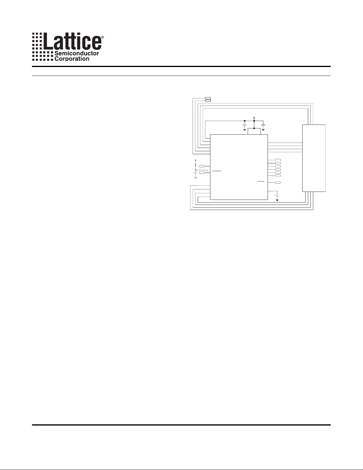
The ispPAC-POWR604 device has six comparators to monitor various power supply levels. The comparators each
have a programmable trip point that is programmed by the user at design time. The output of the comparators feed
into the PLD logic array to drive the state machine logic or monitor logic. The outputs of comparators
COMP1...COMP6 are also routed to external pins to be monitored directly or can be used to drive additional control
logic if expansion is required. The comparator outputs are open-drain type output buffers and require a pull up
resistor to drive a logic high. All six comparators have hysteresis, the hysteresis is dependent on the voltage trip
point scale that is set, it ranges from 3.4mV for the 1.2V monitor supply range to 16.2mV for the 5.0V monitor supply range. The comparators can be set with a trip point from 1.03V to 5.72V, with 192 different values. The application diagram shows a set-up that can monitor and control multiple power supplies. The digital outputs and inputs
are also used to interface with the board that is being powered up.
22

Lattice Semiconductor ispPAC-POWR604 Data Sheet
Figure 13. Typical Application Example: ispPAC-POWR604 Interfacing to CPU Board Using Four Outputs,
Four Inputs and Six VMON Voltage Monitoring Signals
Voltage Monitor 6
Voltage Monitor 5
2.5-5V Supply
V
DD
CARD_RESETN
WDT_IN
INT_ACK
DONE
6 Analog Inputs
VMON1
VMON2
VMON3
VMON4
VMON5
VMON6
CLK
RESET
IN1
IN2
IN3
IN4
VDD VDDINP
ispPAC-POWR604
Power Sequence
Controller
OUT5
OUT6
OUT7
OUT8
Comp1
Comp2
Comp3
Comp4
Comp5
Comp6
POR
CREF
0.1uF1.0uF
Digital
Logic
CPU_RESETN
BROWNOUT_INT
LOAD_ENABLE
POWER_OK
0.1uF
CPU/ASIC
Card etc.
23

Lattice Semiconductor ispPAC-POWR604 Data Sheet
Software-Based Design Environment
Design Entry Software
All functions within the ispPAC-POWR604 are controlled through a Windows-based software development tool
called PAC-Designer. PAC-Designer has an easy-to-use graphical user interface (Figure 14) that allows the user to
set up the ispPAC-POWR604 to perform required functions, such as timed sequences for power supply or monitor
trip points for the voltage monitor inputs. The software tool gives the user control over how the device drives the
outputs and the functional configurations for all I/O pins. User-friendly dialog boxes are provided to set and edit all
of the analog features of the ispPAC-POWR604. An extension to the schematic screen is the LogiBuilder design
environment (Figure 15) that is used to enter and edit control sequences. Again, user-friendly dialog boxes are provided in this window to help the designer quickly implement sequences that take advantage of the powerful built-in
PLD. Once the configurations are chosen and the sequence has been described by the utilities, the device is ready
to program. A standard JTAG interface is used to program the E
ports downloading the device through the PC’s parallel port. The ispPAC-POWR604 can be reprogrammed in-system using the software and an ispDOWNLOAD® Cable assembly to compensate for variations in supply timing,
sequencing or scaling of voltage monitor inputs.
Figure 14. PAC-Designer Schematic Screen
2
CMOS memory. The PAC-Designer software sup-
The user interface (Figure 14) provides access to various internal function blocks within the ispPAC-POWR604
device.
Analog Inputs: Accesses the programmable threshold trip-points for the comparators and pin naming conventions.
Digital Inputs: Digital input naming configurations and digital inputs feed into the internal PLD for the sequence
controller.
Sequence Controller: Incorporates a PLD architecture for designing the state machine to control the order and
functions associated with the user-defined power-up sequence/monitor and control.
Logic Outputs: These pins are configured and assigned in the Logic Output Functional Block. The four digital out-
puts are open-drain and require an external pull-up resistor.
24

Lattice Semiconductor ispPAC-POWR604 Data Sheet
Internal Clock: The internal clock configuration and clock prescaler values are user-programmable, as well as the
four internal programmable timers used for sequence delay.
User Electronic Signature (UES): Stores 16 bits of ID or board information in non-volatile E2CMOS.
Figure 15. PAC-Designer LogiBuilder Screen
Programming of the ispPAC-POWR604 is accomplished using the Lattice ispDOWNLOAD Cable. This cable connects to the parallel port of a PC and is driven through the PAC-Designer software. The software controls the JTAG
TAP interface and shifts in the JEDEC data bits that set the configuration of all the analog and digital circuitry that
the user has defined during the design process.
Power to the device must be set at 3.0V to 5.5V during programming, once the programming steps have been completed, the power supply to the ispPAC-POWR604 can be set from 2.25V to 5V. Once programmed, the on-chip
non-volatile E2CMOS bits hold the entire design configuration for the digital circuits, analog circuits and trip points
for comparators etc. Upon powering the device up, the non-volatile E2CMOS bits control the device configuration. If
design changes need to be made such as adjusting comparator trip points or changes to the digital logic functions,
the device is simply re-programmed using the ispDOWNLOAD Cable.
Design Simulation Capability
Support for functional simulation of the control sequence is provided using the design tools Waveform Editor and
Waveform Viewer. Both applications are spawned from the LogiBuilder environment of PAC-Designer. The simulation engine combines the design file with a stimulus file (edited by the user with the Waveform Editor) to produce an
output file that can be observed with the Waveform Viewer (Figure 16).
25

Lattice Semiconductor ispPAC-POWR604 Data Sheet
Figure 16. PAC-Designer Functional Simulation Screen
In-System Programming
The ispPAC-POWR604 is an in-system programmable device. This is accomplished by integrating all E2CMOS
configuration memory and control logic on-chip. Programming is performed through a 4-wire, IEEE 1149.1 compliant serial JTAG interface. Once a device is programmed, all configuration information is stored on-chip, in non-volatile E2CMOS memory cells. The specifics of the IEEE 1149.1 serial interface and all ispPAC-POWR604
instructions are described in the JTAG interface section of this data sheet.
User Electronic Signature
The User Electronic Signature (UES), allows the designer to include identification bits or serial numbers inside the
device, stored in E2CMOS memory. The ispPAC-POWR604 contains 16 UES bits that can be configured by the
user to store unique data such as ID codes, revision numbers or inventory control codes.
Electronic Security
An Electronic Security Fuse (ESF) bit is provided to prevent unauthorized readout of the E2CMOS bit pattern. Once
programmed, this cell prevents further access to the functional user bits in the device. This cell can only be erased
by reprogramming the device; this way the original configuration cannot be examined or copied once programmed.
Usage of this feature is optional.
Production Programming Support
Once a final configuration is determined, an ASCII format JEDEC file can be created using the PAC-Designer software. Devices can then be ordered through the usual supply channels with the user’s specific configuration already
preloaded into the devices. By virtue of its standard interface, compatibility is maintained with existing production
programming equipment, giving customers a wide degree of freedom and flexibility in production planning.
26

Lattice Semiconductor ispPAC-POWR604 Data Sheet
Package Diagrams
44-Pin TQFP (Dimensions in Millimeters)
PIN 1 INDICATOR
D
3
A
A-B0.20 C44XD
E
B
e
8
D
3
3
TOP VIEW
SIDE VIEW
SEE DETAIL 'A'
b
0.20
MD
A-BC
c
SEATING PLANE
b
b
1
LEAD FINISH
c
1
C
BASE METAL
SECTION B-B
NOTES:
1. DIMENSIONING AND TOLERANCING PER ANSI Y14.5 - 1982.
2. ALL DIMENSIONS ARE IN MILLIMETERS.
DATUMS A, B AND D TO BE DETERMINED AT DATUM PLANE H.
3.
4. DIMENSIONS D1 AND E1 DO NOT INCLUDE MOLD PROTRUSION.
ALLOWABLE MOLD PROTRUSION IS 0.254 MM ON D1 AND E1
DIMENSIONS.
5. THE TOP OF PACKAGE MAY BE SMALLER THAN THE BOTTOM
OF THE PACKAGE BY 0.15 MM.
6. SECTION B-B:
THESE DIMENSIONS APPLY TO THE FLAT SECTION OF THE
LEAD BETWEEN 0.10 AND 0.25 MM FROM THE LEAD TIP.
7. A1 IS DEFINED AS THE DISTANCE FROM THE SEATING PLANE
TO THE LOWEST POINT ON THE PACKAGE BODY.
EXACT SHAPE OF EACH CORNER IS OPTIONAL.
8.
0.10 C
DETAIL 'A'
E1
DH A-B4X 0.20
A
A2
A1
SYMBOL MIN.
D1
BOTTOM VIEW
H
B
0.20 MIN.
B
1.00 REF.
NOM.
A
A1
A2 1.35
D
D1
E 12.00 BSC
E1
N
e
b
b1
c
c1 0.09 0.13
-
0.05
0.45L
0.30
0.30
0.09
-
-
1.40
12.00 BSC
10.00 BSC
10.00 BSC
0.60
44
0.80 BSC
0.37
0.35
0.15
GAUGE PLANE
0.25
0-7∞
L
MAX.
1.60
0.15
1.45
0.75
0.45
0.40
0.20
0.16
27

Lattice Semiconductor ispPAC-POWR604 Data Sheet
Part Number Description
ispPAC-POWR604 - 01XX44X
Device Family
Device Number
ispPAC-POWR604 Ordering Information
Conventional Packaging
Industrial
Part Number Package Pins
ispPAC-POWR604-01T44I TQFP 44
Automotive
Part Number Package Pins
ispPAC-POWR604-01T44E TQFP 44
Lead-Free Packaging
Lead-Free Industrial
Operating Temperature Range
I = Industrial (-40°C to +85°C)
E = Automotive (-40°C to +125°C)
Package
T = 44-pin TQFP
TN = Lead-Free 44-pin TQFP
Performance Grade
01 = Standard
Part Number Package Pins
ispPAC-POWR604-01TN44I TQFP 44
Lead-Free Automotive
Part Number Package Pins
ispPAC-POWR604-01TN44E TQFP 44
28

Lattice Semiconductor ispPAC-POWR604 Data Sheet
Package Options
6
5
4
3
N
N
N
N
NC
NC
NC
NC
NC
NC
VMO
VMO
VMO
CREF
VMO
44
43
1
NC
2
NC
3
NC
4
NC
IN1
IN2
IN3
IN4
5
ispPAC-POWR604
6
7
8
9
10
11
12 13 14 15 16 17 18 19 20 21 22
OUT6
OUT5
VDD
RESET
VDDINP
Note: NC is no connect.
42
41
40
39
38
37
44-pin TQFP
OUT8
COMP6
NC
OUT7
NC
COMP5
36
COMP4
35
COMP3
34
33
32
31
30
29
28
27
26
25
24
23
COMP2
VMON2
VMON1
TMS
TDI
TRST
TDO
GND
CLK
POR
TCK
COMP1
29
 Loading...