

■
■
■
■
■
■
■
■
®
ispPAC-POWR1220AT8
In-System Programmable Power Supply
Monitoring, Sequencing and Margining Controller
August 2007 Data Sheet DS1015
Features
Monitor, Control, and Margin Multiple
Power Supplies
• Simultaneously monitors up to 12 power
supplies
• Provides up to 20 output control signals
• Provides up to eight analog outputs for
margining/trimming power supply voltages
• Programmable digital and analog circuitry
Power Supply Margin and Trim Functions
• Trim and margin up to eight power supplies
• Dynamic voltage control through I
• Four hardware selectable voltage profiles
• Independent Digital Closed-Loop Trim function
for each output
Embedded PLD for Sequence Control
• 48-macrocell CPLD implements both state
machines and combinatorial logic functions
Embedded Programmable Timers
• Four independent timers
• 32µs to 2 second intervals for timing sequences
Analog Input Monitoring
• 12 independent analog monitor inputs
• Differential inputs for remote ground sense
• Two programmable threshold comparators per
analog input
• Hardware window comparison
• 10-bit ADC for I
2
C monitoring
High-Voltage FET Drivers
• Power supply ramp up/down control
• Programmable current and voltage output
• Independently configurable for FET control or
digital output
2-Wire (I
• Comparator status monitor
• ADC readout
• Direct control of inputs and outputs
• Power sequence control
• Dynamic trimming/margining control
2
C/SMBus™ Compatible) Interface
2
C
Application Block Diagram
Primary
Supply
Primary
Supply
Primary
Supply
Primary
Supply
Primary
Supply
3.3V
2.5V
1.8V
POL#1
POL#N
Power Supply
Margin/Trim
Control Block
ADC
12 Analog Inputs
and Voltage Monitors
ispPAC-POWR1220AT8
8 Analog
Trim
Outputs
4 Timers
n
igraM/
m
ir
T
Enables
16 Digital
Outputs
48 Macrocells
6 Digital
Inputs
Other Control/Supervisory
Signals
4 MOSFET
Drivers
CPLD
83 Inputs
2
C
I
Interface
I
Bus
2
Voltage
C
itry
u
Other Board Circ
Monitoring
CPU
Digital Monitoring
Description
Lattice’s Power Manager II ispPAC-POWR1220AT8 is a
general-purpose power-supply monitor, sequence and
margin controller, incorporating both in-system programmable logic and in-system programmable analog
functions implemented in non-volatile E
nology. The ispPAC-POWR1220AT8 device provides 12
independent analog input channels to monitor up to 12
power supply test points. Each of these input channels
offers a differential input to support remote ground
sensing, and has two independently programmable
comparators to support both high/low and in-bounds/
out-of-bounds (window-compare) monitor functions. Six
general-purpose digital inputs are also provided for miscellaneous control functions.
2
CMOS
®
tech-
3.3V Operation, Wide Supply Range 2.8V to
3.96V
• In-system programmable through JTAG
• Industrial temperature range: -40°C to +85°C
• 100-pin TQFP package, lead-free option
© 2007 Lattice Semiconductor Corp. All Lattice trademarks, registered trademarks, patents, and disclaimers are as listed at www.latticesemi.com/legal. All other
brand or product names are trademarks or registered trademarks of their respective holders. The specifications and information herein are subject to change without
notice.
www.latticesemi.com
The ispPAC-POWR1220AT8 provides 20 open-drain
digital outputs that can be used for controlling DC-DC
converters, low-drop-out regulators (LDOs) and optocouplers, as well as for supervisory and general-purpose logic interface functions. Four of these outputs
1
DS1015_01.4
Lattice Semiconductor ispPAC-POWR1220AT8 Data Sheet
(HVOUT1-HVOUT4) may be configured as high-voltage MOSFET drivers. In high-voltage mode these outputs can
provide up to 10V for driving the gates of n-channel MOSFETs so that they can be used as high-side power
switches controlling the supplies with a programmable ramp rate for both ramp up and ramp down.
The ispPAC-POWR1220AT8 incorporates a 48-macrocell CPLD that can be used to implement complex state
machine sequencing for the control of multiple power supplies as well as combinatorial logic functions. The status
of all of the comparators on the analog input channels as well as the general purpose digital inputs are used as
inputs by the CPLD array, and all digital outputs may be controlled by the CPLD. Four independently programmable
timers can create delays and time-outs ranging from 32µs to 2 seconds. The CPLD is programmed using LogiBuilder™, an easy-to-learn language integrated into the PAC-Designer
monitor the status of any of the analog input channel comparators or the digital inputs.
In addition to the sequence control functions, the ispPAC-POWR1220AT8 incorporates eight DACs for generating
trimming voltage to control the output voltage of a DC-DC converter. The trimming voltage can be set to four hardware selectable preset values (voltage profiles) or can be dynamically loaded in to the DAC through the I
Additionally, each power supply output voltage can be maintained typically within 0.5% tolerance across various
load conditions using the Digital Closed Loop Control mode. The operating voltage profile can either be selected
using external hardware pins or through the PLD outputs.
The on-chip 10-bit A/D converter can both be used to monitor the V
implementing digital closed loop mode for maintaining the output voltage of all power supplies controlled by the
monitoring and trimming section of the ispPAC-POWR1220AT8 device.
2
The I
C bus/SMBus interface allows an external microcontroller to measure the voltages connected to the V
inputs, read back the status of each of the V
comparator and PLD outputs, control logic signals IN2 to IN5, con-
MON
trol the output pins, and load the DACs for the generation of the trimming voltage of the external DC-DC converter.
®
software. Control sequences are written to
voltage through the I
MON
2
C bus as well as for
2
C bus.
MON
Figure 1. ispPAC-POWR1220AT8 Block Diagram
VPS0
VPS1
VMON1+
VMON1GS
VMON2+
VMON2GS
VMON3+
VMON3GS
VMON4+
VMON4GS
VMON5+
VMON5GS
VMON6+
VMON6GS
VMON7+
VMON7GS
VMON8+
VMON8GS
VMON9+
VMON9GS
VMON10+
VMON10GS
VMON11+
VMON11GS
VMON12+
VMON12GS
IN1
IN2
IN3
IN4
IN5
IN6
A
N
D
V
O
L
T
A
E G
N O M
I
T
O
R
S
6
I
N
D
P
I
G
I
T
T U
A
S
L
VCCINP
1
2
A
N
A
L
O
G
I
N
P
S T U
VCCD (3)
VCCA
V
C
C
P
R
O
G
ADC
JTAG LOGIC
V
T
T
T
C
C
D
K
C
O
S M
J
OSCILLATOR
S
A
T
E
D
T
D
L
I
T
I
D
I
MARGIN/TRIM
CONTROL LOGIC
CPLD
48 MACROCELLS
83 INPUTS
CLOCK
P
M
L
C
L
C D
K
L
K
R
T E S E
b
TIMERS
(4)
VOLTAGE OUTPUT
DACS (8)
DAC
DAC
DAC
DAC
DAC
O
U
T
P
U
P
T
O
R
O
O
L
U
T
G N I
I2C
INTERFACE
S
S
C
L
GNDA (2)
D
A
DAC
DAC
DAC
TRIM1
TRIM2
TRIM3
TRIM4
TRIM5
TRIM6
TRIM7
TRIM8
D
R
I
V
R E
S
G I D
T I
L A
O
T U
P
U
T
S
4
F
E
T
1
6
O
P
E
N
D
R
I A
N
GNDD (6)
HVOUT1
HVOUT2
HVOUT3
HVOUT4
OUT5/SMBA
OUT6
OUT7
OUT8
OUT9
OUT10
OUT11
OUT12
OUT13
OUT14
OUT15
OUT16
OUT17
OUT18
OUT19
OUT20
2

Lattice Semiconductor ispPAC-POWR1220AT8 Data Sheet
Pin Descriptions
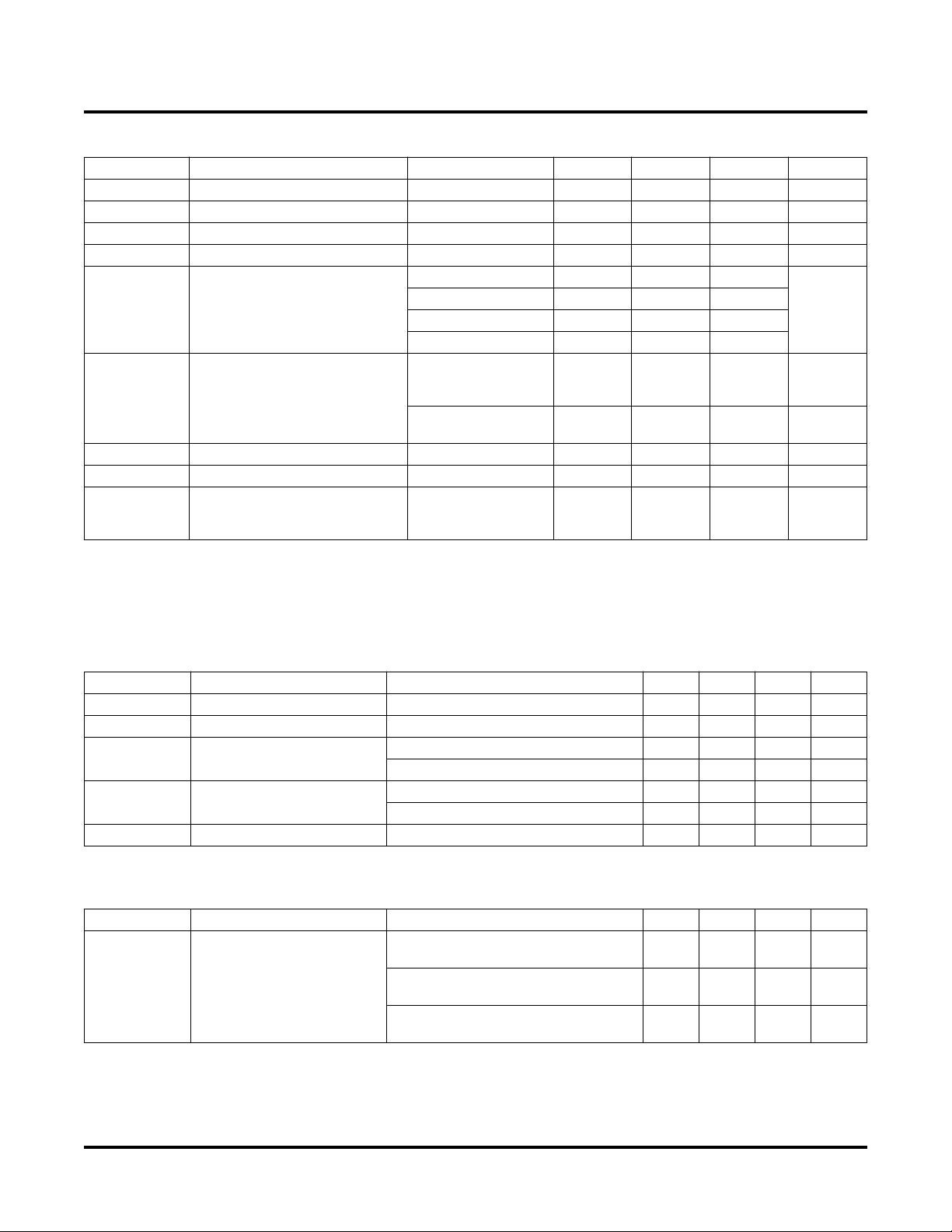
Number Name Pin Type Voltage Range Description
89 VPS0 Digital Input VCCD Trim Select Input 0 Registered by MCLK
90 VPS1 Digital Input VCCD Trim Select Input 1 Registered by MCLK
97 IN1
1IN2
2IN3
4IN4
6IN5
7IN6
2
3
3
3
3
3
Digital Input VCCINP
Digital Input VCCINP
Digital Input VCCINP
Digital Input VCCINP
Digital Input VCCINP
Digital Input VCCINP
47 VMON1 Analog Input -0.3V to 5.75V
46 VMON1GS Analog Input -0.2V to 0.3V
50 VMON2 Analog Input -0.3V to 5.75V
48 VMON2GS Analog Input -0.2V to 0.3V
52 VMON3 Analog Input -0.3V to 5.75V
51 VMON3GS Analog Input -0.2V to 0.3V
54 VMON4 Analog Input -0.3V to 5.75V
53 VMON4GS Analog Input -0.2V to 0.3V
56 VMON5 Analog Input -0.3V to 5.75V
55 VMON5GS Analog Input -0.2V to 0.3V
58 VMON6 Analog Input -0.3V to 5.75V
57 VMON6GS Analog Input -0.2V to 0.3V
62 VMON7 Analog Input -0.3V to 5.75V
61 VMON7GS Analog Input -0.2V to 0.3V
64 VMON8 Analog Input -0.3V to 5.75V
63 VMON8GS Analog Input -0.2V to 0.3V
66 VMON9 Analog Input -0.3V to 5.75V
65 VMON9GS Analog Input -0.2V to 0.3V
68 VMON10 Analog Input -0.3V to 5.75V
67 VMON10GS Analog Input -0.2V to 0.3V
70 VMON11 Analog Input -0.3V to 5.75V
69 VMON11GS Analog Input -0.2V to 0.3V
72 VMON12 Analog Input -0.3V to 5.75V
71 VMON12GS Analog Input -0.2V to 0.3V
3, 22, 36,
43, 88, 98
45, 87 GNDA
13, 38, 94 VCCD
60 VCCA
GNDD
8
8
7
7
Ground Ground Digital Ground
Ground Ground Analog Ground
Power 2.8V to 3.96V Core VCC, Main Power Supply
Power 2.8V to 3.96V Analog Power Supply
5 VCCINP Power 2.25V to 3.6VVCC for IN[1:6] Inputs
33 VCCJ Power 2.25V to 3.6VVCC for JTAG Logic Interface Pins
39 VCCPROG Power 3.0V to 3.6V
6
0V to 10V Open-Drain Output 1
12.5µA to 100µA Source
100µA to 3000µA Sink
86 HVOUT1
Open Drain Output
Current Source/Sink
1
1
1
1
1
1
4
5
4
5
4
5
4
5
4
5
4
5
4
5
4
5
4
5
4
5
4
5
4
5
PLD Logic Input 1 Registered by MCLK
PLD Logic Input 2 Registered by MCLK
PLD Logic Input 3 Registered by MCLK
PLD Logic Input 4 Registered by MCLK
PLD Logic Input 5 Registered by MCLK
PLD Logic Input 6 Registered by MCLK
Voltage Monitor 1 Input
Voltage Monitor 1 Ground Sense
Voltage Monitor 2 Input
Voltage Monitor 2 Ground Sense
Voltage Monitor 3 Input
Voltage Monitor 3 Ground Sense
Voltage Monitor 4 Input
Voltage Monitor 4 Ground Sense
Voltage Monitor 5 Input
Voltage Monitor 5 Ground Sense
Voltage Monitor 6 Input
Voltage Monitor 6 Ground Sense
Voltage Monitor 7 Input
Voltage Monitor 7 Ground Sense
Voltage Monitor 8 Input
Voltage Monitor 8 Ground Sense
Voltage Monitor 9 Input
Voltage Monitor 9 Ground Sense
Voltage Monitor 10 Input
Voltage Monitor 10 Ground Sense
Voltage Monitor 11 Input
Voltage Monitor 11 Ground Sense
Voltage Monitor 12 Input
Voltage Monitor 12 Ground Sense
VCC for E
Not Powered by V
2
Programming when the Device is
CCD
or V
CCA
High-voltage FET Gate Driver 1
3

Lattice Semiconductor ispPAC-POWR1220AT8 Data Sheet
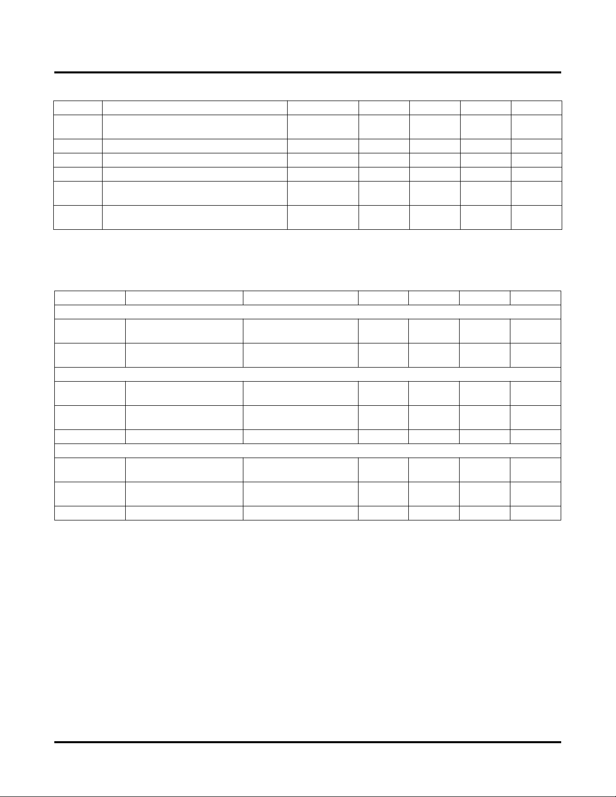
Pin Descriptions (Cont.)
Number Name Pin Type Voltage Range Description
Open Drain Output
85 HVOUT2
Current Source/Sink
Open Drain Output
42 HVOUT3
Current Source/Sink
Open Drain Output
40 HVOUT4
Current Source/Sink
8 OUT5_SMBA Open Drain Output
9 OUT6 Open Drain Output
10 OUT7 Open Drain Output
11 OUT8 Open Drain Output
12 OUT9 Open Drain Output
14 OUT10 Open Drain Output
15 OUT11 Open Drain Output
16 OUT12 Open Drain Output
17 OUT13 Open Drain Output
18 OUT14 Open Drain Output
19 OUT15 Open Drain Output
20 OUT16 Open Drain Output
21 OUT17 Open Drain Output
23 OUT18 Open Drain Output
24 OUT19 Open Drain Output
25 OUT20 Open Drain Output
84 TRIM1 Analog Output
83 TRIM2 Analog Output
82 TRIM3 Analog Output
80 TRIM4 Analog Output
79 TRIM5 Analog Output
75 TRIM6 Analog Output
74 TRIM7 Analog Output
6
0V to 10V Open-Drain Output 2
12.5µA to 100µA Source
100µA to 3000µA Sink
6
0V to 10V Open-Drain Output 3
12.5µA to 100µA Source
100µA to 3000µA Sink
6
0V to 10V Open-Drain Output 4
12.5µA to 100µA Source
100µA to 3000µA Sink
6
0V to 5.5V
6
0V to 5.5V Open-Drain Output 6
6
0V to 5.5V Open-Drain Output 7
6
0V to 5.5V Open-Drain Output 8
6
0V to 5.5V Open-Drain Output 9
6
0V to 5.5V Open-Drain Output 10
6
0V to 5.5V Open-Drain Output 11
6
0V to 5.5V Open-Drain Output 12
6
0V to 5.5V Open-Drain Output 13
6
0V to 5.5V Open-Drain Output 14
6
0V to 5.5V Open-Drain Output 15
6
0V to 5.5V Open-Drain Output 16
6
0V to 5.5V Open-Drain Output 17
6
0V to 5.5V Open-Drain Output 18
6
0V to 5.5V Open-Drain Output 19
6
0V to 5.5V Open-Drain Output 20
High-voltage FET Gate Driver 2
High-voltage FET Gate Driver 3
High-voltage FET Gate Driver 4
Open-Drain Output 5, (SMBUS Alert Active
Low)
-320mV to +320mV
from Programmable
Trim DAC Output 1
DAC Offset
-320mV to +320mV
from Programmable
Trim DAC Output 2
DAC Offset
-320mV to +320mV
from Programmable
Trim DAC Output 3
DAC Offset
-320mV to +320mV
from Programmable
Trim DAC Output 4
DAC Offset
-320mV to +320mV
from Programmable
Trim DAC Output 5
DAC Offset
-320mV to +320mV
from Programmable
Trim DAC Output 6
DAC Offset
-320mV to +320mV
from Programmable
Trim DAC Output 7
DAC Offset
4

Lattice Semiconductor ispPAC-POWR1220AT8 Data Sheet
Pin Descriptions (Cont.)
Number Name Pin Type Voltage Range Description
73 TRIM8 Analog Output
91 RESETb
9
Digital I/O 0V to 3.96V Device Reset (Active Low)
95 PLDCLK Digital Output 0V to 3.96V
96 MCLK Digital I/O 0V to 3.96V 8MHz Clock I/O (Tristate), CMOS Drive
34 TDO Digital Output 0V to 5.5V JTAG Test Data Out
37 TCK Digital Input 0V to 5.5V JTAG Test Clock Input
28 TMS Digital Input 0V to 5.5V JTAG Test Mode Select
31 TDI Digital Input 0V to 5.5V JTAG Test Data In, TDISEL pin = 1
30 ATDI Digital Input 0V to 5.5V JTAG Test Data In (Alternate), TDISEL Pin = 0
32 TDISEL Digital Input 0V to 5.5V Select TDI/ATDI Input
92 SCL Digital Input 0V to 5.5V I
93 SDA Digital I/O 0V to 5.5V I
44, 59 RESERVED Reserved - Do Not Connect
26, 27, 29,
35, 41, 49,
76, 77, 78,
NC No Internal Connection
81, 99, 100
1. [IN1...IN6] are inputs to the PLD. The thresholds for these pins are referenced by the voltage on VCCINP.
2. IN1 pin can also be controlled through JTAG interface.
3. [IN2..IN6] can also be controlled through I
4. The VMON inputs can be biased independently from VCCA. Unused VMONs should be tied to GNDD.
5. The VMONGS inputs are the ground sense line for each given VMON pin. The VMON input pins along with the VMONGS ground sense
pins implement a differential pair for each voltage monitor to allow remote sense at the load. VMONGS lines must be connected and are
not to exceed -0.2V - +0.3V in reference to the GNDA pin.
6. Open-drain outputs require an external pull-up resistor to a supply.
7. VCCD and VCCA pins must be connected together on the circuit board.
8. GNDA and GNDD pins must be connected together on the circuit board.
9. The RESETb pin should only
be used for cascading two or more ispPAC-POWR1220AT8 devices.
2
C/SMBus interface.
-320mV to +320mV
from Programmable
DAC Offset
Trim DAC Output 8
250kHz PLD Clock Output (Tristate), CMOS
Output
2
C Serial Clock Input
2
C Serial Data, Bi-directional Pin
5
Lattice Semiconductor ispPAC-POWR1220AT8 Data Sheet
Absolute Maximum Ratings
Absolute maximum ratings are shown in the table below. Stresses beyond those listed may cause permanent damage to the device. Functional operation of the device at these or any other conditions beyond those indicated in the
recommended operating conditions of this specification is not implied.
Symbol Parameter Conditions Min. Max. Units
V
CCD
V
CCA
V
CCINP
V
CCJ
V
CCPROG
V
IN
V
MON+
V
MONGS
V
TRI
I
SINKMAXTOTAL
T
S
T
A
Core supply -0.5 4.5 V
Analog supply -0.5 4.5 V
Digital input supply (IN[1:6]) -0.5 6 V
JTAG logic supply -0.5 6 V
2
E
programming supply -0.5 4 V
Digital input voltage (all digital I/O pins) -0.5 6 V
V
input voltage -0.5 6 V
MON
V
input voltage ground sense -0.5 6 V
MON
Voltage applied to tri-stated pins
HVOUT[1:4] -0.5 11 V
OUT[5:20] -0.5 6 V
Maximum sink current on any output 23 mA
Storage temperature -65 150
Ambient temperature -65 125
o
C
o
C
Recommended Operating Conditions
Symbol Parameter Conditions Min. Max. Units
V
CCD,
V
CCINP
V
CCJ
V
CCPROG
V
IN
V
MON
V
MONGS
V
CCA
Core supply voltage at pin 2.8 3.96 V
Digital input supply for IN[1:6] at pin 2.25 5.5 V
JTAG logic supply voltage at pin 2.25 3.6 V
E2 programming supply at pin During E2 programming 3.0 3.6 V
Input voltage at digital input pins -0.3 5.5 V
Input voltage at V
Input voltage at V
pins -0.3 5.9 V
MON
pins -0.2 0.3 V
MONGS
OUT[5:20] pins -0.3 5.5 V
V
OUT
T
APROG
T
A
Open-drain output voltage
Ambient temperature during
programming
HVOUT[1:4] pins in opendrain mode
-0.3 10.4 V
-40 85
Ambient temperature Power applied -40 85
Analog Specifications
Symbol Parameter Conditions Min. Typ. Max. Units
1
I
CC
I
CCINP
I
CCJ
I
CCPROG
1. Includes currents on V
Supply current 40 mA
Supply current 5mA
Supply current 1mA
Supply current During programming cycle 40 mA
CCD
and V
CCA
supplies.
o
C
o
C
6
Lattice Semiconductor ispPAC-POWR1220AT8 Data Sheet
Voltage Monitors
Symbol Parameter Conditions Min. Typ. Max. Units
R
IN
C
IN
V
Range Programmable trip-point range 0.075 5.734 V
MON
Sense Near-ground sense threshold 70 75 80 mV
V
Z
Accuracy Absolute accuracy of any trip-point
V
MON
HYST
Input resistance 55 65 75 kΩ
Input capacitance 8 pF
1
Hysteresis of any trip-point (relative to
setting)
0.2 0.7 %
1%
CMR Common mode rejection 60 dB
1. Guaranteed by characterization across V
range, operating temperature, process.
CCA
High Voltage FET Drivers
Symbol Parameter Conditions Min. Typ. Max. Units
10V setting 9.6 10 10.4
V
PP
I
OUTSRC
I
OUTSINK
Gate driver output voltage
Gate driver source current
(HIGH state)
Gate driver sink current
(LOW state)
6V setting 5.8 6 6.2
12.5
Four settings in
software
25
50
100
FAST OFF mode 2000 3000
100
Controlled ramp
settings
250
500
V8V setting 7.7 8 8.3
µA
µA
7
Lattice Semiconductor ispPAC-POWR1220AT8 Data Sheet
Margin/Trim DAC Output Characteristics
Symbol Parameter Conditions Min Typ Max Units
Resolution 8(7+sign) bits
FSR Full scale range +/-320 mV
LSB LSB step size 2.5 mV
I
OUT
BPZ
TS
C_LOAD Maximum load capacitance 50 pF
T
UPDATEM
TOSE
1. To 1% of set value with 50pf load connected to trim pins.
2. Total time required to update a single TRIMx output value by setting the associated DAC through the I2C port.
3. This is the total resultant error in the trimmed power supply output voltage referred to any DAC code due to the DAC’s INL, DNL, gain, output impedance, offset error and bipolar offset error across the industrial temperature range and the ispPAC-POWR1200AT8 operating V
and V
CCD
Output source/sink current -200 200 µA
Offset 1 0.6
Bipolar zero output voltage
(code=80h)
Offset 2 0.8
Offset 3 1.0
Offset 4 1.25
DAC code changed
TrimCell output voltage settling
1
time
Update time through I2C port
Total open loop supply voltage
3
error
ranges.
from 80H to FFH or
80H to 00H
Single DAC code
change
2
MCLK = 8MHz 260 µs
256 µs
Full scale DAC corresponds to ±5% supply
-1% +1% V/V
voltage variation
2.5 ms
V
CCA
ADC Characteristics
Symbol Parameter Conditions Min. Typ. Max. Units
ADC Resolution 10 Bits
T
CONVERT
V
IN
ADC Step Size LSB
Eattenuator Error Due to Attenuator Programmable Attenuator = 3 +/- 0.1 %
1. Maximum voltage is limited by V
ADC Error Budget Across Entire Operating Temperature Range
Symbol Parameter Conditions Min. Typ. Max. Units
TADC Error
1. Total error, guaranteed by characterization, includes INL, DNL, Gain, Offset, and PSR specs of the ADC.
Conversion Time Time from I2C Request 200 µs
Input range Full Scale
Programmable Attenuator = 1 0 2.048 V
Programmable Attenuator = 3 0 5.9
1
Programmable Attenuator = 1 2 mV
Programmable Attenuator = 3 6 mV
pin (theoretical maximum is 6.144V).
MONX
Total Measurement Error at
Any Voltage
1
Measurement Range 600 mV - 2.048V,
VMONxGS > -100mV, Attenuator =1
Measurement Range 600 mV - 2.048V,
VMONxGS > -200mV, Attenuator =1
Measurement Range 0 - 2.048V,
VMONxGS > -200mV, Attenuator =1
-8 +/-4 8 mV
+/-6 mV
+/-10 mV
V
8
Lattice Semiconductor ispPAC-POWR1220AT8 Data Sheet
Power-On Reset
Symbol Parameter Conditions Min. Typ. Max. Units
T
GOOD
V
TL
V
TH
V
T
T
POR
C
L
1. Corresponds to VCCA and VCCD supply voltages.
Power-on reset to valid VMON comparator
output
Threshold below which RESETb is LOW
Threshold above which RESETb is HIGH
Threshold above which RESETb is valid
Minimum duration dropout required to trigger
RESETb
Capacitive load on RESETb for master/slave
operation
1
1
1
2.5 ms
2.3 V
2.7 V
0.8 V
15µs
200 pF
AC/Transient Characteristics
Over Recommended Operating Conditions
Symbol Parameter Conditions Min. Typ. Max. Units
Voltage Monitors
t
PD16
t
PD64
Propagation delay input to
output glitch filter OFF
Propagation delay input to
output glitch filter ON
Oscillators
f
CLK
f
CLKEXT
f
PLDCLK
Internal master clock
frequency (MCLK)
Externally applied master
clock (MCLK)
PLDCLK output frequency f
Timers
Timeout Range
Resolution
Range of programmable
timers (128 steps)
Spacing between available
adjacent timer intervals
Accuracy Timer accuracy f
7.6 8 8.4 MHz
7.2 8.8 MHz
= 8MHz 250 kHz
CLK
f
= 8MHz 0.032 1966 ms
CLK
= 8MHz -6.67 -12.5 %
CLK
16 µs
64 µs
13 %
9

Lattice Semiconductor ispPAC-POWR1220AT8 Data Sheet
Digital Specifications
Over Recommended Operating Conditions
Symbol Parameter Conditions Min. Typ. Max. Units
I
IL,IIH
I
OH-HVOUT
I
PU
V
IL
V
IH
V
OL
V
OH
I
SINKTOTAL
1. VPS[0:1], SCL, SDA referenced to V
Input leakage, no pull-up/pull-down +/-10 µA
HVOUT[1:4] in open
Output leakage current
drain mode and pulled
35 60 µA
up to 10V
Input pull-up current (TMS, TDI,
TDISEL, ATDI, MCLK)
70 µA
VPS[0:1], TDI, TMS,
ATDI, TDISEL, 3.3V
0.8
supply
Voltage input, logic low
1
VPS[0:1], TDI, TMS,
ATDI, TDISEL, 2.5V
0.7
V
supply
SCL, SDA 30% V
IN[1:6] 30% V
CCD
CCINP
VPS[0:1], TDI, TMS,
ATDI, TDISEL, 3.3V
2.0
supply
Voltage input, logic high
1
VPS[0:1], TDI, TMS,
ATDI, TDISEL, 2.5V
1.7
V
supply
HVOUT[1:4] (open drain mode), I
TDO,MCLK,PLDCLK I
TDO, MCLK, PLDCLK I
SCL, SDA 70% V
IN[1:6] 70% V
= 10mA 0.8
SINK
= 20mA 0.8
SINK
= 4mA 0.4
SINK
= 4mA V
SRC
CCD
CCINP
V
CCD
V
CCINP
- 0.4 V
CCD
VOUT[5:20] I
All digital outputs 130 mA
; IN[1:6] referenced to V
CCD
; TDO, TDI, TMS, ATDI, TDISEL referenced to V
CCINP
CCJ
.
10

Lattice Semiconductor ispPAC-POWR1220AT8 Data Sheet
I2C Port Characteristics
100KHz 400KHz
Symbol Definition
F
I2C
T
SU;STA
T
HD;STA
T
SU;DAT
T
SU;STO
T
HD;DAT
T
LOW
T
HIGH
T
F
T
R
T
TIMEOUT
T
POR
T
BUF
1. If F
is less than 50kHz, then the ADC DONE status bit is not guaranteed to be set after a valid conversion request is completed. In this
I2C
case, waiting for the T
readout. When F
I2C clock/data rate 100
After start 4.7 0.6 us
After start 4 0.6 us
Data setup 250 100 ns
Stop setup 4 0.6 us
Data hold; SCL= Vih_min = 2.1V 0.3 3.45 0.3 0.9 us
Clock low period 4.7 1.3 us
Clock high period 4 0.6 us
Fall time; 2.25V to 0.65V 300 300 ns
Rise time; 0.65V to 2.25V 1000 300 ns
Detect clock low timeout 25 35 25 35 ms
Device must be operational after power-on reset 500 500 ms
Bus free time between stop and start condition 4.7 1.3 us
CONVERT
is greater than 50kHz, ADC conversion complete is ensured by waiting for the DONE status bit.
I2C
minimum time after a convert request is made is the only way to guarantee a valid conversion is ready for
1
400
UnitsMin. Max. Min. Max.
1
KHz
11
Lattice Semiconductor ispPAC-POWR1220AT8 Data Sheet
Timing for JTAG Operations
Symbol Parameter Conditions Min. Typ. Max. Units
t
ISPEN
t
ISPDIS
t
HVDIS
t
HVDIS
t
CEN
t
CDIS
t
SU1
t
H
t
CKH
t
CKL
f
MAX
t
CO
t
PWV
t
PWP
Figure 2. Erase (User Erase or Erase All) Timing Diagram
Program enable delay time 10 — — µs
Program disable delay time 30 — — µs
High voltage discharge time, program 30 — — µs
High voltage discharge time, erase 200 — — µs
Falling edge of TCK to TDO active — — 15 ns
Falling edge of TCK to TDO disable — — 15 ns
Setup time 5 — — ns
Hold time 10 — — ns
TCK clock pulse width, high 20 — — ns
TCK clock pulse width, low 20 — — ns
Maximum TCK clock frequency — — 25 MHz
Falling edge of TCK to valid output — — 15 ns
Verify pulse width 30 — — µs
Programming pulse width 20 — — ms
VIH
TMS
VIL
t
SU1
VIH
TCK
VIL
Update-IR Run-Test/Idle (Erase) Select-DR Scan
State
t
t
SU1
H
t
CKH tGKL
t
H
Figure 3. Programming Timing Diagram
VIH
TMS
VIL
TCK
State
t
SU1
VIH
VIL
Update-IR Run-Test/Idle (Program) Select-DR Scan
t
t
SU1
H
t
t
CKL
CKH
CKH
t
SU1
t
SU2
t
t
SU1
H
t
CKL
t
H
t
CKH
t
H
t
CKH
t
SU1
t
H
t
H
t
CKH
t
SU1
t
PWP
t
t
SU1
Instruction, then clock to the Run-Test/Idle state
Clock to Shift-IR state and shift in the Discharge
t
H
CKH
t
t
SU1
H
t
t
CKH
GKL
Run-Test/Idle (Discharge)
t
SU1
t
H
t
CKH
Specified by the Data Sheet
t
Update-IR
Clock to Shift-IR state and shift in the next
Instruction, which will stop the discharge process
12
Lattice Semiconductor ispPAC-POWR1220AT8 Data Sheet
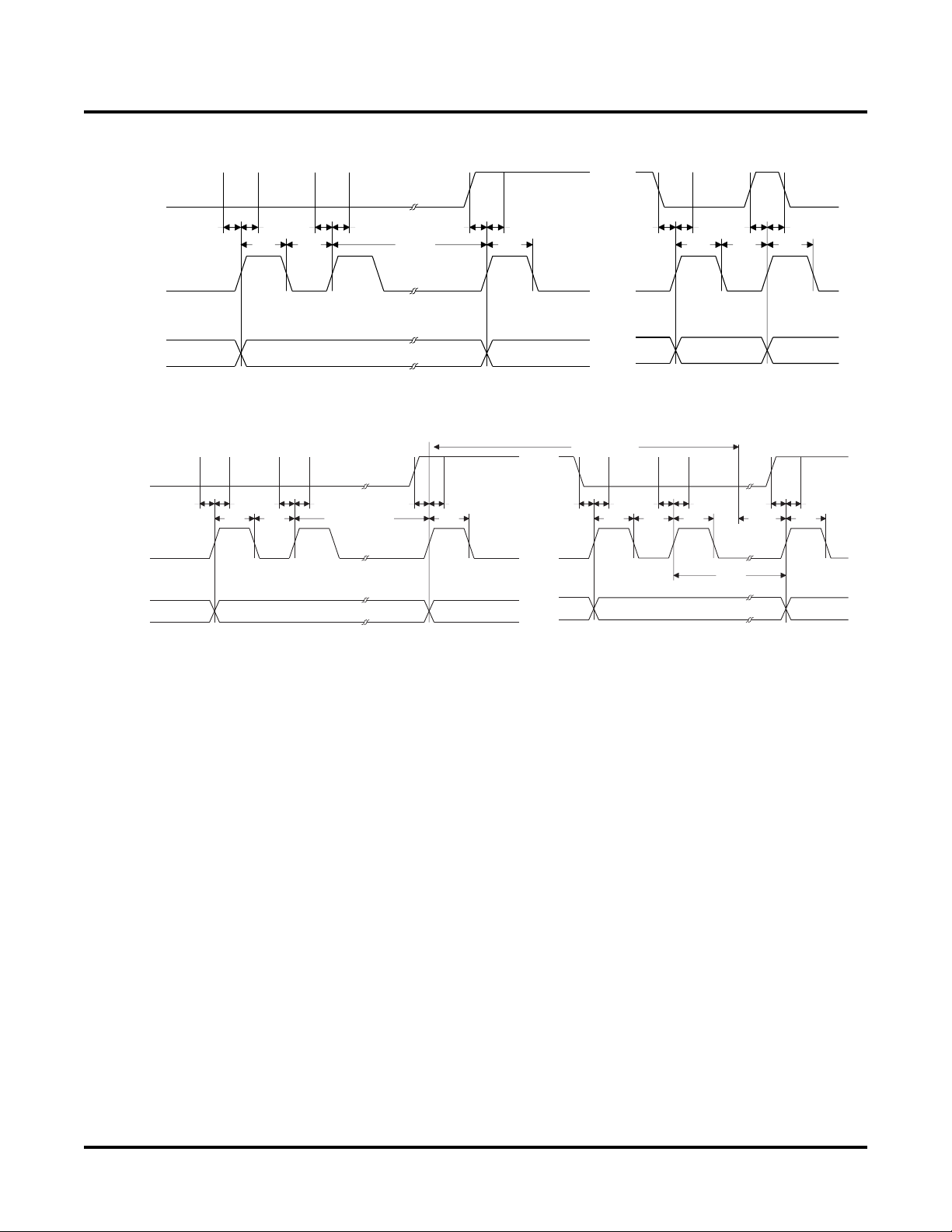
Figure 4. Verify Timing Diagram
VIH
TMS
VIL
t
H
t
CKH
TCK
VIH
VIL
t
t
SU1
t
H
SU1
t
t
CKH
CKL
t
H
t
SU1
t
PWV
t
H
t
CKH
t
SU1
t
t
H
SU1
t
t
CKH
CKL
State
Update-IR Run-Test/Idle (Program) Select-DR Scan
Update-IR
Clock to Shift-IR state and shift in the next Instruction
Figure 5. Discharge Timing Diagram
t
(Actual)
t
SU1
Clock to Shift-IR state and shift in the Verify
Instruction, then clock to the Run-Test/Idle state
HVDIS
t
t
H
SU1
t
t
CKH
CKL
Run-Test/Idle (Verify)
t
H
t
CKH
Specified by the Data Sheet
t
SU1
t
PWV
Actual
t
PWV
t
H
t
CKH
TMS
TCK
State
VIH
VIL
t
H
VIH
VIL
t
t
SU1
t
H
SU1
t
CKH tCKL
Update-IR Run-Test/Idle (Erase or Program)
t
SU1
t
PWP
t
H
t
CKH
Select-DR Scan
Theory of Operation
Analog Monitor Inputs
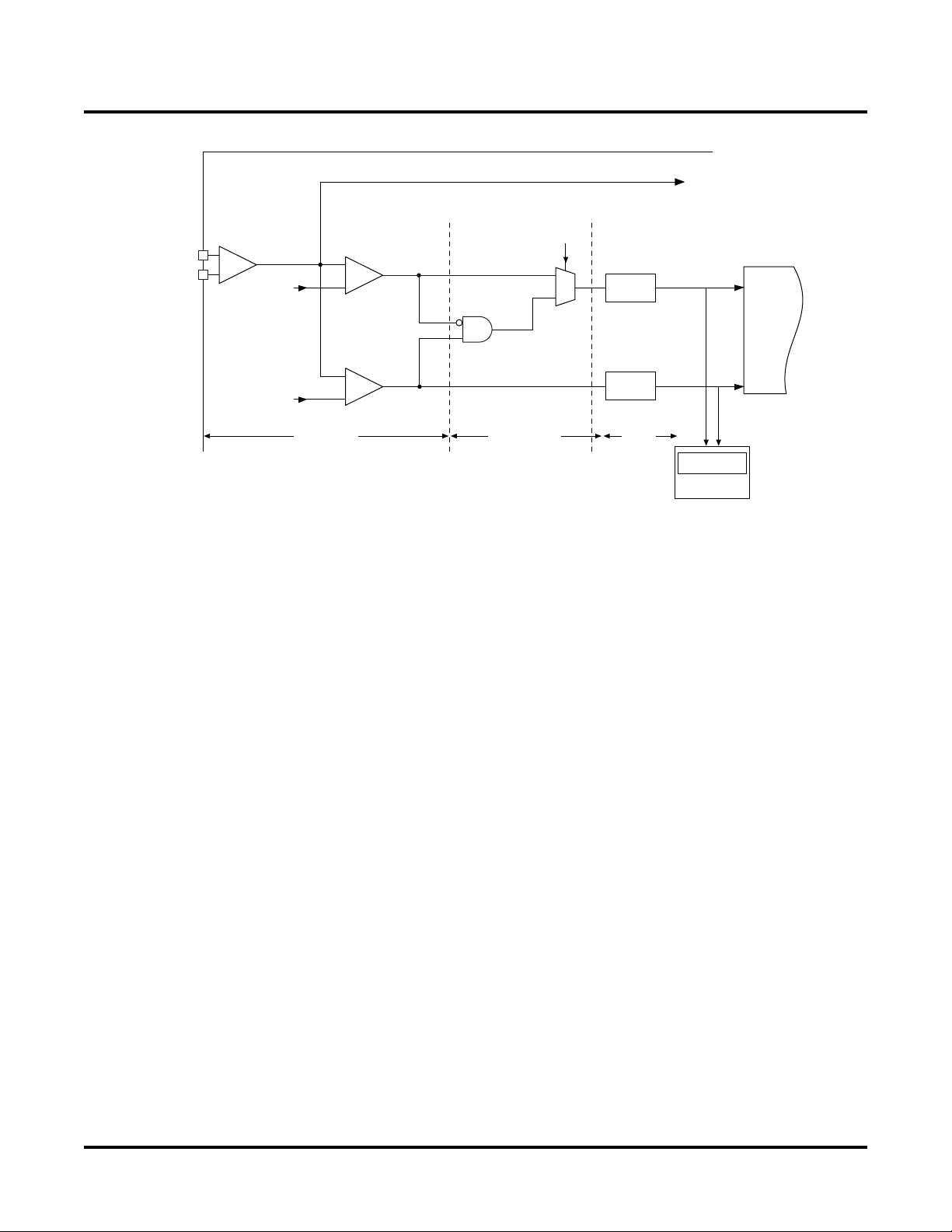
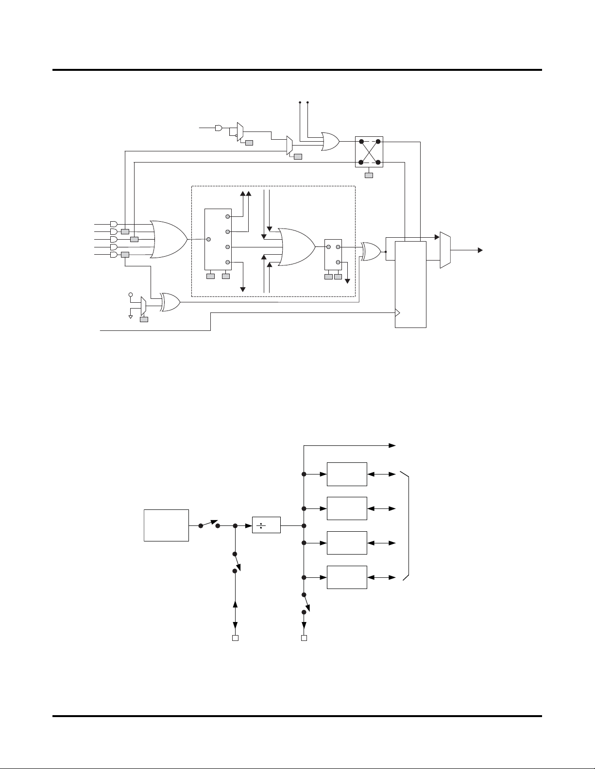
The ispPAC-POWR1220AT8 provides 12 independently programmable voltage monitor input circuits as shown in
Figure 6. Two individually programmable trip-point comparators are connected to an analog monitoring input. Each
comparator reference has 368 programmable trip points over the range of 0.664V to 5.734V. Additionally, a 75mV
‘zero-detect’ threshold is selectable which allows the voltage monitors to determine if a monitored signal has
dropped to ground level. This feature is especially useful for determining if a power supply’s output has decayed to
a substantially inactive condition after it has been switched off.
13
Lattice Semiconductor ispPAC-POWR1220AT8 Data Sheet
Figure 6. ispPAC-POWR1220AT8 Voltage Monitors
ispPAC-POWR1220AT8
To ADC
Comp A/Window
Select
Window Control
MUX
Glitch
Filter
Glitch
Filter
Filtering
VMONxA
Logic
Signal
VMONxB
Logic
Signal
VMONx Status
I2C Interface
Unit
PLD
Array
VMONx
VMONxGS
Differential
Input Buffer x
Trip Point A
Trip Point B
Comp A
+
–
Comp B
+
–
Analog Input
Figure 6 shows the functional block diagram of one of the 12 voltage monitor inputs - ‘x’ (where x = 1...12). Each
voltage monitor can be divided into three sections: Analog Input, Window Control, and Filtering. The first section
provides a differential input buffer to monitor the power supply voltage through VMONx+ (to sense the positive ter-
minal of the supply) and VMONxGS (to sense the power supply ground). Differential voltage sensing minimizes
inaccuracies in voltage measurement with ADC and monitor thresholds due to the potential difference between the
ispPAC-POWR1220AT8 device ground and the ground potential at the sensed node on the circuit board.
The voltage output of the differential input buffer is monitored by two individually programmable trip-point comparators, shown as CompA and CompB. Table 1 shows all 368 trip points spanning the range 0.664V to 5.734V to
which a comparator’s threshold can be set.
Each comparator outputs a HIGH signal to the PLD array if the voltage at its positive terminal is greater than its programmed trip point setting, otherwise it outputs a LOW signal.
A hysteresis of approximately 1% of the setpoint is provided by the comparators to reduce false triggering as a
result of input noise. The hysteresis provided by the voltage monitor is a function of the input divider setting. Table 3
lists the typical hysteresis versus voltage monitor trip-point.
AGOOD Logic Signal
All the VMON comparators auto-calibrate immediately after a power-on reset event. During this time, the digital
glitch filters are also initialized. This process completion is signalled by an internally generated logic signal:
AGOOD. All logic using the VMON comparator logic signals must wait for the AGOOD signal to become active.
Programmable Over-Voltage and Under-Voltage Thresholds
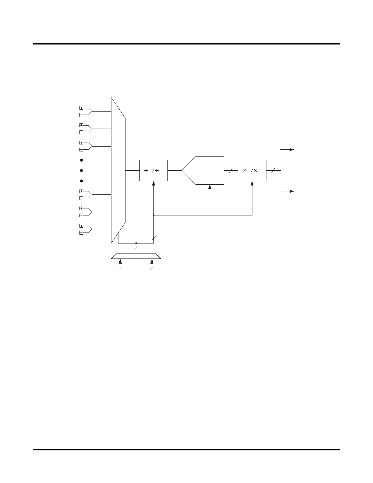
Figure 7 (a) shows the power supply ramp-up and ramp-down voltage waveforms. Because of hysteresis, the comparator outputs change state at different thresholds depending on the direction of excursion of the monitored power
supply.
14
Lattice Semiconductor ispPAC-POWR1220AT8 Data Sheet
Figure 7. (a) Power Supply Voltage Ramp-up and Ramp-down Waveform and the Resulting Comparator
Output, (b) Corresponding to Upper and Lower Trip Points
UTP
LTP
(a)
Monitored Power Supply Votlage
(b)
Comparator Logic Output
During power supply ramp-up the comparator output changes from logic 0 to 1 when the power supply voltage
crosses the upper trip point (UTP). During ramp down the comparator output changes from logic state 1 to 0 when
the power supply voltage crosses the lower trip point (LTP). To monitor for over voltage fault conditions, the UTP
should be used. To monitor under-voltage fault conditions, the LTP should be used.
Tables 1 and 2 show both the under-voltage and over-voltage trip points, which are automatically selected in software depending on whether the user is monitoring for an over-voltage condition or an under-voltage condition.
15

Lattice Semiconductor ispPAC-POWR1220AT8 Data Sheet
Table 1. Trip Point Table Used For Over-Voltage Detection
Fine
Range
Setting
1 0.790 0.941 1.120 1.333 1.580 1.885 2.244 2.665 3.156 3.758 4.818 5.734
2 0.786 0.936 1.114 1.326 1.571 1.874 2.232 2.650 3.139 3.738 4.792 5.703
3 0.782 0.930 1.108 1.319 1.563 1.864 2.220 2.636 3.123 3.718 4.766 5.674
4 0.778 0.926 1.102 1.312 1.554 1.854 2.209 2.622 3.106 3.698 4.741 5.643
5 0.773 0.921 1.096 1.305 1.546 1.844 2.197 2.607 3.089 3.678 4.715 5.612
6 0.769 0.916 1.090 1.298 1.537 1.834 2.185 2.593 3.072 3.657 4.689 5.581
7 0.765 0.911 1.084 1.290 1.529 1.825 2.173 2.579 3.056 3.637 4.663 5.550
8 0.761 0.906 1.078 1.283 1.520 1.815 2.161 2.565 3.039 3.618 4.638 5.520
9 0.756 0.901 1.072 1.276 1.512 1.805 2.149 2.550 3.022 3.598 4.612 5.489
10 0.752 0.896 1.066 1.269 1.503 1.795 2.137 2.536 3.005 3.578 4.586 5.459
11 0.748 0.891 1.060 1.262 1.495 1.785 2.125 2.522 2.988 3.558 4.561 5.428
12 0.744 0.886 1.054 1.255 1.486 1.774 2.113 2.507 2.971 3.537 4.535 5.397
13 0.739 0.881 1.048 1.248 1.478 1.764 2.101 2.493 2.954 3.517 4.509 5.366
14 0.735 0.876 1.042 1.240 1.470 1.754 2.089 2.479 2.937 3.497 4.483 5.336
15 0.731 0.871 1.036 1.233 1.461 1.744 2.077 2.465 2.920 3.477 4.457 5.305
16 0.727 0.866 1.030 1.226 1.453 1.734 2.064 2.450 2.903 3.457 4.431 5.274
17 0.723 0.861 1.024 1.219 1.444 1.724 2.052 2.436 2.886 3.437 4.406 5.244
18 0.718 0.856 1.018 1.212 1.436 1.714 2.040 2.422 2.869 3.416 4.380 5.213
19 0.714 0.851 1.012 1.205 1.427 1.704 2.028 2.407 2.852 3.396 4.355 5.183
20 0.710 0.846 1.006 1.198 1.419 1.694 2.016 2.393 2.836 3.376 4.329 5.152
21 0.706 0.841 1.000 1.190 1.410 1.684 2.004 2.379 2.819 3.356 4.303 5.121
22 0.701 0.836 0.994 1.183 1.402 1.673 1.992 2.365 2.802 3.336 4.277 5.090
23 0.697 0.831 0.988 1.176 1.393 1.663 1.980 2.350 2.785 3.316 4.251 5.059
24 0.693 0.826 0.982 1.169 1.385 1.653 1.968 2.337 2.768 3.296 4.225 5.030
25 0.689 0.821 0.976 1.162 1.376 1.643 1.956 2.323 2.752 3.276 4.199 4.999
26 0.684 0.816 0.970 1.155 1.369 1.633 1.944 2.309 2.735 3.256 4.174 4.968
27 0.680 0.810 0.964 1.148 1.361 1.623 1.932 2.294 2.718 3.236 4.149 4.937
28 0.676 0.805 0.958 1.140 1.352 1.613 1.920 2.280 2.701 3.216 4.123 4.906
29 0.672 0.800 0.952 1.133 1.344 1.603 1.908 2.266 2.684 3.196 4.097 4.876
30 0.668 0.795 0.946 1.126 — 1.593 1.896 2.251 — 3.176 4.071 4.845
Low-V
Sense
123456789101112
Coarse Range Setting
75mV
16

Lattice Semiconductor ispPAC-POWR1220AT8 Data Sheet
Table 2. Trip Point Table Used For Under-Voltage Detection
Fine
Range
Setting
1 0.786 0.936 1.114 1.326 1.571 1.874 2.232 2.650 3.139 3.738 4.792 5.703
2 0.782 0.930 1.108 1.319 1.563 1.864 2.220 2.636 3.123 3.718 4.766 5.674
3 0.778 0.926 1.102 1.312 1.554 1.854 2.209 2.622 3.106 3.698 4.741 5.643
4 0.773 0.921 1.096 1.305 1.546 1.844 2.197 2.607 3.089 3.678 4.715 5.612
5 0.769 0.916 1.090 1.298 1.537 1.834 2.185 2.593 3.072 3.657 4.689 5.581
6 0.765 0.911 1.084 1.290 1.529 1.825 2.173 2.579 3.056 3.637 4.663 5.550
7 0.761 0.906 1.078 1.283 1.520 1.815 2.161 2.565 3.039 3.618 4.638 5.520
8 0.756 0.901 1.072 1.276 1.512 1.805 2.149 2.550 3.022 3.598 4.612 5.489
9 0.752 0.896 1.066 1.269 1.503 1.795 2.137 2.536 3.005 3.578 4.586 5.459
10 0.748 0.891 1.060 1.262 1.495 1.785 2.125 2.522 2.988 3.558 4.561 5.428
11 0.744 0.886 1.054 1.255 1.486 1.774 2.113 2.507 2.971 3.537 4.535 5.397
12 0.739 0.881 1.048 1.248 1.478 1.764 2.101 2.493 2.954 3.517 4.509 5.366
13 0.735 0.876 1.042 1.240 1.470 1.754 2.089 2.479 2.937 3.497 4.483 5.336
14 0.731 0.871 1.036 1.233 1.461 1.744 2.077 2.465 2.920 3.477 4.457 5.305
15 0.727 0.866 1.030 1.226 1.453 1.734 2.064 2.450 2.903 3.457 4.431 5.274
16 0.723 0.861 1.024 1.219 1.444 1.724 2.052 2.436 2.886 3.437 4.406 5.244
17 0.718 0.856 1.018 1.212 1.436 1.714 2.040 2.422 2.869 3.416 4.380 5.213
18 0.714 0.851 1.012 1.205 1.427 1.704 2.028 2.407 2.852 3.396 4.355 5.183
19 0.710 0.846 1.006 1.198 1.419 1.694 2.016 2.393 2.836 3.376 4.329 5.152
20 0.706 0.841 1.000 1.190 1.410 1.684 2.004 2.379 2.819 3.356 4.303 5.121
21 0.701 0.836 0.994 1.183 1.402 1.673 1.992 2.365 2.802 3.336 4.277 5.090
22 0.697 0.831 0.988 1.176 1.393 1.663 1.980 2.350 2.785 3.316 4.251 5.059
23 0.693 0.826 0.982 1.169 1.385 1.653 1.968 2.337 2.768 3.296 4.225 5.030
24 0.689 0.821 0.976 1.162 1.376 1.643 1.956 2.323 2.752 3.276 4.199 4.999
25 0.684 0.816 0.970 1.155 1.369 1.633 1.944 2.309 2.735 3.256 4.174 4.968
26 0.680 0.810 0.964 1.148 1.361 1.623 1.932 2.294 2.718 3.236 4.149 4.937
27 0.676 0.805 0.958 1.140 1.352 1.613 1.920 2.280 2.701 3.216 4.123 4.906
28 0.672 0.800 0.952 1.133 1.344 1.603 1.908 2.266 2.684 3.196 4.097 4.876
29 0.668 0.795 0.946 1.126 1.335 1.593 1.896 2.251 2.667 3.176 4.071 4.845
30 0.664 0.790 0.940 1.119 — 1.583 1.884 2.236 — 3.156 4.045 4.815
Low-V
Sense
123456789101112
Coarse Range Setting
75mV
17

Lattice Semiconductor ispPAC-POWR1220AT8 Data Sheet
Table 3. Comparator Hysteresis vs. Trip-Point
Trip-point Range (V)
Hysteresis (mV)Low Limit High Limit
0.664 0.79 8
0.79 0.941 10
0.94 1.12 12
1.119 1.333 14
1.326 1.58 17
1.583 1.885 20
1.884 2.244 24
2.236 2.665 28
2.65 3.156 34
3.156 3.758 40
4.045 4.818 51
4.815 5.734 61
75 mV 0 (Disabled)
The window control section of the voltage monitor circuit is an AND gate (with inputs: an inverted COMPA “ANDed”
with COMPB signal) and a multiplexer that supports the ability to develop a ‘window’ function without using any of
the PLD’s resources. Through the use of the multiplexer, voltage monitor’s ‘A’ output may be set to report either the
status of the ‘A’ comparator, or the window function of both comparator outputs. The voltage monitor’s ‘A’ output
indicates whether the input signal is between or outside the two comparator thresholds. Important: This windowing
function is only valid in cases where the threshold of the ‘A’ comparator is set to a value higher than that of the ‘B’
comparator. Table 4 shows the operation of window function logic.
Table 4. Voltage Monitor Windowing Logic
Input Voltage Comp A Comp B
< Trip-point B < Trip-point A 0 0 0 Outside window, low
V
IN
Trip-point B < V
Trip-point B < Trip-point A < V
< Trip-point A 0 1 1 Inside window
IN
IN
1 1 0 Outside window, high
Window
(B and Not A) Comment
Note that when the ‘A’ output of the voltage monitor circuit is set to windowing mode, the ‘B’ output continues to
monitor the output of the ‘B’ comparator. This can be useful in that the ‘B’ output can be used to augment the windowing function by determining if the input is above or below the windowing range.
The third section in the ispPAC-POWR1220AT8’s input voltage monitor is a digital filter. When enabled, the comparator output will be delayed by a filter time constant of 64 µS, and is especially useful for reducing the possibility of
false triggering from noise that may be present on the voltages being monitored. When the filter is disabled, the
comparator output will be delayed by 16µS. In both cases, enabled or disabled, the filters also provide synchronization of the input signals to the PLD clock. This synchronous sampling feature effectively eliminates the possibility of
race conditions from occurring in any subsequent logic that is implemented in the ispPAC-POWR1220AT8’s internal PLD logic.
2
The comparator status can be read from the I
C interface. For details on the I2C interface, please refer to the I2C/
SMBUS Interface section of this data sheet.
18
Lattice Semiconductor ispPAC-POWR1220AT8 Data Sheet
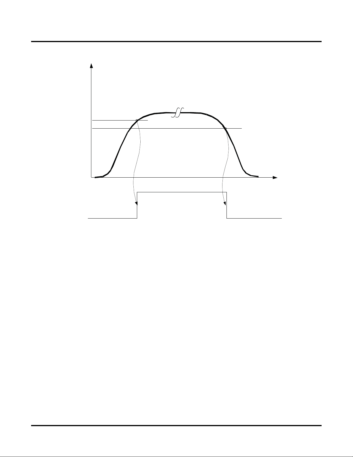
VMON Voltage Measurement with the On-chip Analog to Digital Converter (ADC)
The ispPAC-POWR1220 has an on-chip analog to digital converter that can be used for measuring the voltages at
the VMON inputs. The ADC is also used in closed loop trimming of DC-DC converters. Close loop trimming is covered later in this document.
Figure 8. ADC Monitoring VMON1 to VMON12
VMON1
VMON2
VMON3
VMON12
VDDA
VDDINP
ADC
MUX
4
5 5
From Closed
Loop Trim
Circuit
Programmable
Analog
Attenuator
3 1
1
5
From I2C
ADC MUX
Register
ADC
Internal
VREF-
2.048V
Internal
Control Signal
Programmable
Multiplier
10
Digital
31
To Closed
Loop Trim
Circuit
12
2
C
To I
Readout
Register
Figure 8 shows the ADC circuit arrangement within the ispPAC-POWR1220AT8 device. The ADC can measure all
analog input voltages through the multiplexer, ADC MUX. The programmable attenuator between the ADC mux and
the ADC can be configured as divided-by-3 or divided-by-1 (no attenuation). The divided-by-3 setting is used to
measure voltages from 0V to 6V range and divided-by-1 setting is used to measure the voltages from 0V to 2V
range.
A microcontroller can place a request for any VMON voltage measurement at any time through the I2C bus. Upon
the receipt of an I2C command, the ADC will be connected to the I2C selected VMON through the ADC MUX. The
ADC output is then latched into the I2C readout registers.
Calculation
The algorithm to convert the ADC code to the corresponding voltage takes into consideration the attenuation bit
value. In other words, if the attenuation bit is set, then the 10-bit ADC result is automatically multiplied by 3 to calculate the actual voltage at that V
input. Thus, the I2C readout register is 12 bits instead of 10 bits. The following
MON
formula can always be used to calculate the actual voltage from the ADC code.
Voltage at the VMONx Pins
VMON = ADC code (12 bits1, converted to decimal) * 2mV
1
Note: ADC_VALUE_HIGH (8 bits), ADC_VALUE_LOW (4 bits) read from I2C/SMBUS interface
19
Lattice Semiconductor ispPAC-POWR1220AT8 Data Sheet
PLD Block
Figure 9 shows the ispPAC-POWR1220AT8 PLD architecture, which is derived from the Lattice's ispMACH™ 4000
CPLD. The PLD architecture allows the flexibility in designing various state machines and control functions used for
power supply management. The AND array has 83 inputs and generates 243 product terms. These 243 product
terms are divided into three groups of 81 for each of the generic logic blocks, GLB1, GLB2, and GLB3. Each GLB
is made up of 16 macrocells. In total, there are 48 macrocells in the ispPAC-POWR1220AT8 device. The output signals of the ispPAC-POWR1220AT8 device are derived from GLBs as shown in Figure 9. Additionally, the GLB3
generates the timer control and trimming block controls.
Figure 9. ispPAC-POWR1220AT8 PLD Architecture
Global Reset
(Resetb pin)
GLB1
AGOOD
IN[1:6]
Generic Logic Block
81
6
16 Macrocell
81 PT
HVOUT[1..4],
OUT[5..8]
VMON[1-12]
Output
Feedback
Timer0
Timer1
Timer2
Timer3
Timer Clock
AND Array
83 Inputs
IRP
243 PT
14
24
4
48
81
81
PLD Clock
GLB2
Generic Logic Block
16 Macrocell
81 PT
GLB3
Generic Logic Block
16 Macrocell
81 PT
OUT[9..16]
OUT[17..20]
PLD_CLT_EN,
PLD_VPS[0:1]
Macrocell Architecture
The macrocell shown in Figure 10 is the heart of the PLD. The basic macrocell has five product terms that feed the
OR gate and the flip-flop. The flip-flop in each macrocell is independently configured. It can be programmed to
function as a D-Type or T-Type flip-flop. Combinatorial functions are realized by bypassing the flip-flop. The polarity
control and XOR gates provide additional flexibility for logic synthesis. The flip-flop’s clock is driven from the common PLD clock that is generated by dividing the 8 MHz master clock by 32. The macrocell also supports asynchronous reset and preset functions, derived from either product terms, the global reset input, or the power-on reset
signal. The resources within the macrocells share routing and contain a product term allocation array. The product
term allocation array greatly expands the PLD’s ability to implement complex logical functions by allowing logic to
be shared between adjacent blocks and distributing the product terms to allow for wider decode functions.
20
Lattice Semiconductor ispPAC-POWR1220AT8 Data Sheet
C
Figure 10. ispPAC-POWR1220AT8 Macrocell Block Diagram
Global Reset Power On Reset
Global Polarity Fuse for
Init Product Term
Product Term Allocation
RP
D/T Q
CLK
Macrocell flip-flop provides
D, T, or combinatorial
output with polarity
To ORP
PT4
PT3
PT2
PT1
PT0
Block Init Product Term
Polarity
Clock
Clock and Timer Functions
Figure 11 shows a block diagram of the ispPAC-POWR1220AT8’s internal clock and timer systems. The master
clock operates at a fixed frequency of 8MHz, from which a fixed 250kHz PLD clock is derived.
Figure 11. Clock and Timer System
lock
PLD
Timer 0
Internal
Oscillator
8MHz
SW0
32
SW1
MCLK PLDCLK
SW2
Timer 1
To/From
PLD
Timer 2
Timer 3
The internal oscillator runs at a fixed frequency of 8 MHz. This signal is used as a source for the PLD and timer
clocks. It is also used for clocking the comparator outputs and clocking the digital filters in the voltage monitor cir-
21
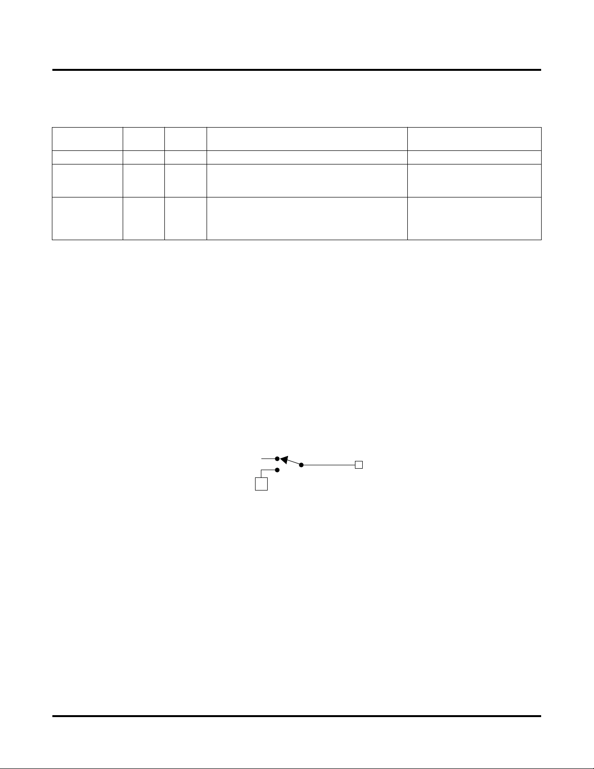
Lattice Semiconductor ispPAC-POWR1220AT8 Data Sheet
cuits, ADC and trim circuits. The ispPAC-POWR1220AT8 can be programmed to operate in three modes: Master
mode, Standalone mode and Slave mode. Table 5 summarizes the operating modes of ispPAC-POWR1220AT8.
Table 5. ispPAC-POWR1220AT8 Operating Modes
Timer
Operating Mode SW0 SW1 Condition Comments
Standalone Closed Open When only one ispPAC-POWR1220AT8 is used. MCLK pin tristated
Master Closed Closed
Slave Open Closed
When more than one ispPAC-POWR1220AT8 is
used in a board, one of them should be configured
to operate in this mode.
When more than one ispPAC-POWR1220AT8s is
used in a board. Other than the master, the rest of
the ispPAC-POWR1220AT8s should be programmed as slaves.
MCLK pin outputs 8MHz clock
MCLK pin is input
A divide-by-32 prescaler divides the internal 8MHz oscillator (or external clock, if selected) down to 250kHz for the
PLD clock and for the programmable timers. This PLD clock may be made available on the PLDCLK pin by closing
SW2. Each of the four timers provides independent timeout intervals ranging from 32µs to 1.96 seconds in 128
steps.
Digital Outputs
The ispPAC-POWR1220AT8 provides 20 digital outputs, HVOUT[1:4] and OUT[5:20]. Outputs OUT[5:20] are permanently configured as open drain to provide a high degree of flexibility when interfacing to logic signals, LEDs,
opto-couplers, and power supply control inputs. The HVOUT[1:4] pins can be configured as either high voltage FET
drivers or open drain outputs. Each of these outputs may be controlled either from the PLD or from the I2C bus. The
determination whether a given output is under PLD or I2C control may be made on a pin-by-pin basis (see
Figure 12). For further details on controlling the outputs through I2C, please see the I2C/SMBUS Interface section of
this data sheet.
Figure 12. Digital Output Pin Configuration
Digital Control
from PLD
Digital Control
2
C Register
from I
OUTx
Pin
High-Voltage Outputs
In addition to being usable as digital open-drain outputs, the ispPAC-POWR1220AT8’s HVOUT1-HVOUT4 output
pins can be programmed to operate as high-voltage FET drivers. Figure 13 shows the details of the HVOUT gate
drivers. Each of these outputs may be controlled from the PLD or from the I2C bus (see Figure 13). For further
details on controlling the outputs through I2C, please see the I2C/SMBUS Interface section of this data sheet.
22
Lattice Semiconductor ispPAC-POWR1220AT8 Data Sheet
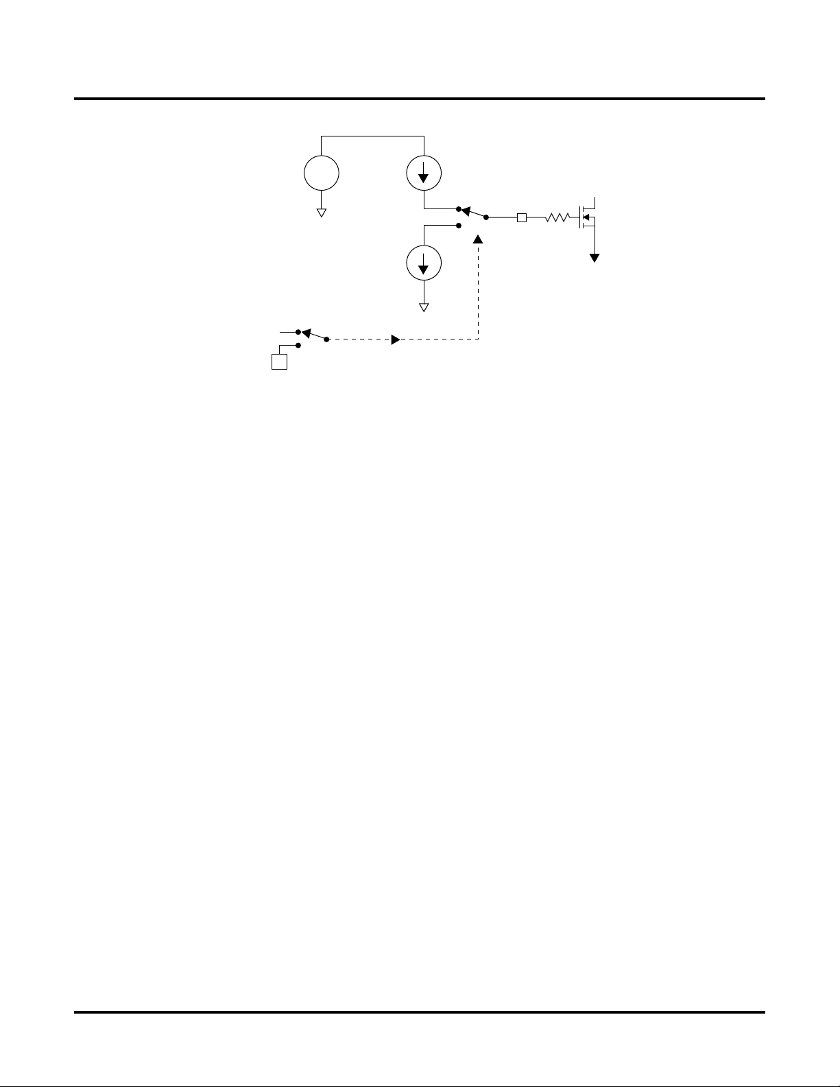
Figure 13. Basic Function Diagram for an Output in High Voltage MOSFET Gate Driver Mode
Charge Pump
(6 to 10V)
+
-
I
SOURCE
(12.5 to 100 µA)
HVOUTx
Input
Supply
Pin
Digital Control
from PLD
from I
(100 to 500 µA)
+Fast Turn-off
Digital Control
2
C Register
I
SINK
(3000µA)
Load
Figure 13 shows the HVOUT circuitry when programmed as a FET driver. In this mode the output either sources
current from a charge pump or sinks current. The maximum voltage that the output level at the pin will rise to is also
programmable between 6V and 10V. The maximum voltage levels that are required depend on the gate-to-source
threshold of the FET being driven and the power supply voltage being switched. The maximum voltage level needs
to be sufficient to bias the gate-to-source threshold on and also accommodate the load voltage at the FET’s
source, since the source pin of the FET to provide a wide range of ramp rates is tied to the supply of the target
board. When the HVOUT pin is sourcing current, charging a FET gate, the source current is programmable
between 12.5µA and 100µA. When the driver is turned to the off state, the driver will sink current to ground, and
this sink current is also programmable between 3000µA and 100µA to control the turn-off rate.
Programmable Output Voltage Levels for HVOUT1- HVOUT4
There are three selectable steps for the output voltage of the FET drivers when in FET driver mode. The voltage
that the pin is capable of driving to can be programmed from 6V to 10V in 2V steps.
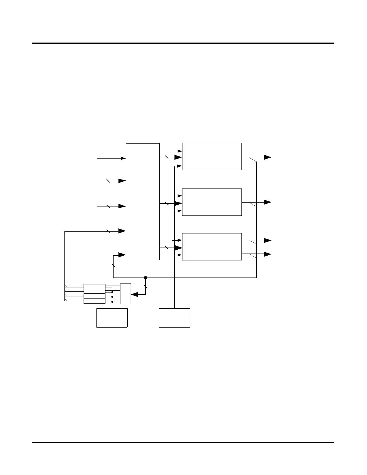
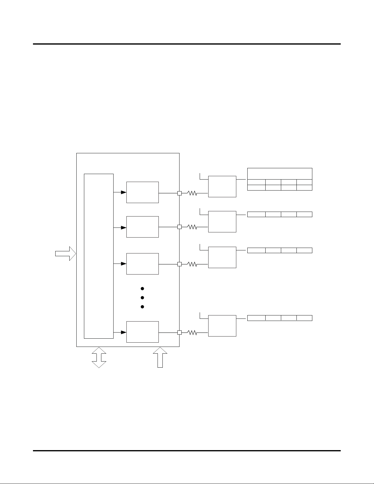
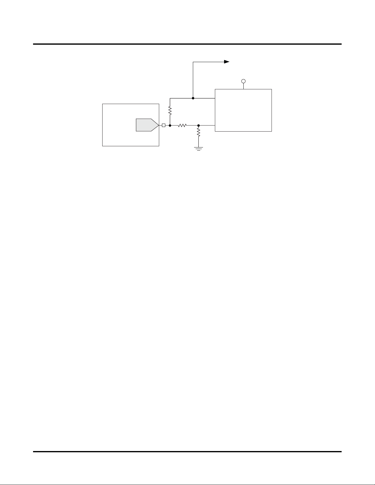
Controlling Power Supply Output Voltage by Margin/ Trim Block
One of the key features of the ispPAC-POWR1220AT8 is its ability to make adjustments to the power supplies that
it may also be monitoring and/or sequencing. This is accomplished through the Trim and Margin Block of the
device. The Trim and Margin Block can adjust voltages of up to eight different power supplies through TrimCells as
shown in Figure 14. The DC-DC blocks in the figure represent virtually any type of DC power supply that has a trim
or voltage adjustment input. This can be an off-the-shelf unit or custom circuit designed around a switching regulator IC.
The interface between the ispPAC-POWR1220AT8 and the DC power supply is represented by a single resistor
(R1 to R8) to simplify the diagram. Each of these resistors represents a resistor network.
Other control signals driving the Margin/Trim Block are:
• VPS [1:0] – Control signals from device pins common to all eight TrimCells, which are used to select the
active voltage profile for all TrimCells together.
• PLD_VPS[1:0] – Voltage profile selection signals generated by the PLD. These signals can be used instead
of the VPS signals from the pins.
• ADC input – Used to determine the trimmed DC-DC converter voltage.
• PLD_CLT_EN – Only from PLD, used to enable closed loop trimming of all TrimCells together.
Next to each DC-DC converter, four voltages are shown. These voltages correspond to the operating voltage profile
of the Margin/Trim Block.
23
Lattice Semiconductor ispPAC-POWR1220AT8 Data Sheet
When the VPS[1:0] = 00, representing Voltage Profile 0: (Voltage Profile 0 is recommended to be used for the nor-
mal circuit operation)
The output voltage of the DC-DC converter controlled by the Trim 1 pin of the ispPAC-POWR1220AT8 will be 1V
and that TrimCell is operating in closed loop trim mode. At the same time, the DC-DC converters controlled by Trim
2, Trim 3 and Trim 8 pins output 1.2V, 1.5V and 3.3V respectively.
When the VPS[1:0] = 01, representing Voltage Profile 1 being active:
The DC-DC output voltage controlled by Trim 1, 2, 3, and 8 pins will be 1.05V, 1.26V, 1.57V, and 3.46V. These sup-
ply voltages correspond to 5% above their respective normal operating voltage (also called as margin high).
Similarly, when VPS[1:0] = 11, all DC-DC converters are margined low by 5%.
Figure 14. ispPAC-POWR1220AT8 Trim and Margin Block
ispPAC-POWR1220AT8
VPS[0:1]
Margin/Trim Block
(Closed Loop)
C Interface Control
2
Digital Closed Loop
and I
TrimCell
#1
TrimCell
#2
(I2C Update)
TrimCell
#3
(I2C Update)
Trim 1
Trim 2
Trim 3
R1*
R2*
R3*
V
IN
DC-DC
Trim-in
V
IN
DC-DC Output Voltage
Controlled by Profiles
0123
1V (CLT) 1.05V 0.97V 0.95V
1.2V (I2C) 1.26V 1.16V 1.14V
DC-DC
Trim-in
V
IN
2
1.5V (I
C) 1.57V 1.45V 1.42V
DC-DC
Trim-in
V
IN
3.3V (EE) 3.46V 3.20V 3.13V
DC-DC
Trim-in
Input From ADC Mux
Read – 10-bit ADC Code
TrimCell
#8
(Register 0)
Trim 8
PLD Control Signals
PLD_CLT_EN,
R8*
*Indicates resistor network
PLD_VPS[0:1]
There are eight TrimCells in the ispPAC-POWR1220AT8 device, enabling simultaneous control of up to eight individual power supplies. Each TrimCell can generate up to four trimming voltages to control the output voltage of the
DC-DC converter.
24
Lattice Semiconductor ispPAC-POWR1220AT8 Data Sheet
Figure 15. TrimCell Driving a Typical DC-DC Converter
V
OUT
V
IN
V
OUT
R
3
R
TrimCell
#N
DAC
1
R
2
Trim
Figure 15 shows the resistor network between the TrimCell #N in the ispPAC-POWR1220AT8 and the DC-DC converter. The values of these resistors depend on the type of DC-DC converter used and its operating voltage range.
The method to calculate the values of the resistors R1, R2, and R3 are described in a separate application note.
Voltage Profile Control
The Margin / Trim Block of ispPAC-POWR1220AT8 consists of eight TrimCells. Because all eight TrimCells in the
Margin / Trim Block are controlled by two common voltage profile control signals, they all operate at the same voltage profile. These common voltage profile control signals are derived from a Control Multiplexer. One set of voltage
profile control inputs to the control multiplexer is from a pair of device pins: VPS0, VPS1. The second set of voltage
profile control inputs is from the PLD: PLD_VPS0, PLD_VPS1. The selection between the two sets of voltage profile control signals is programmable and is stored in the E2CMOS memory.
DC-DC
Converter
25

Lattice Semiconductor ispPAC-POWR1220AT8 Data Sheet
Figure 16. Voltage Profile Control
ispPAC-POWR1220AT8
Margin/Trim Block
VPS0
VPS1
PLD Control Signals
PLD_VPS[0:1]
TrimCell
Trim 1
#1
TrimCell
Trim 2
#2
TrimCell
INT/EXT
SELECT
2
CMOS)
(E
2
CTRL
MUX
2
Common Voltage Profile Control Signals
2
#3
TrimCell
#4
TrimCell
Trim 3
Trim 4
Trim 5
#5
TrimCell
Trim 6
#6
TrimCell
Trim 7
#7
Common Voltage Profile Control Signals
TrimCell
Trim 8
#8
TrimCell Architecture
The TrimCell block diagram is shown in Figure 17. The 8-bit DAC at the output provides the trimming voltage
required to set the output voltage of a programmable supply. Each TrimCell can be operated in any one of the four
voltage profiles. In each voltage profile the output trimming voltage can be set to a preset value. There are six 8-bit
registers in each TrimCell that, depending on the operational mode, set the DAC value. Of these, four DAC values
(DAC Register 0 to DAC Register 3) are stored in the E2CMOS memory while the remaining register contents are
stored in volatile registers. Two multiplexers (Mode Mux and Profile Mux) control the routing of the code to the DAC.
The Profile Mux can be controlled by common TrimCell voltage profile control signals.
26

Lattice Semiconductor ispPAC-POWR1220AT8 Data Sheet
Figure 17. ispPAC-POWR1220AT8 Output TrimCell
TRIMCELL ARCHITECTURE
VOLTAGE
PROFILE 3
VOLTAGE
PROFILE 2
VOLTAGE
PROFILE 1
VOLTAGE
PROFILE 0
DAC REGISTER 3
2
(E
CMOS)
DAC REGISTER 2
2
(E
CMOS)
DAC REGISTER 1
2
(E
CMOS)
DAC REGISTER 0
2
(E
CMOS)
DAC REGISTER
2
(I
C)
CLOSED LOOP
TRIM REGISTER
FROM CLOSED LOOP
TRIM CIRCUIT
8
8
8
8
8
8
VOLTAGE PROFILE 0
MODE
MUX
MODE SELECT
(E2CMOS)
11
10
01
00
8
COMMON TrimCell
VOLTAGE PROFILE
CONTROL
PROFILE
MUX
2
8
DAC
TRIMx
Figure 14 shows four power supply voltages next to each DC-DC converter. When the Profile MUX is set to Voltage
Profile 3, the DC supply controlled by Trim 1 will be at 0.95V, the DC supply controlled by Trim 2 will be at 1.14V,
1.43V for Trim 3 and 3.14V for Trim 8. When Voltage Profile 0 is selected, Trim 1 will set the supply to 1V, Trim 2 and
Trim 3 will be set by the values that have been loaded using I2C at 1.2 and 1.5V, and Trim 8 will be set to 3.3V.
The following table summarizes the voltage profile selection and the corresponding DAC output trimming voltage.
The voltage profile selection is common to all eight TrimCells.
Table 6. TrimCell Voltage Profile and Operating Modes
PLD_VPS[1:0]
or VPS[1:0] Selected Voltage Profile Selected Mode
11 Voltage Profile 3 — DAC Register 3 (E
10 Voltage Profile 2 — DAC Register 2 (E
01 Voltage Profile 1 — DAC Register 1 (E
DAC Register 0 Select DAC Register 0 (E
00 Voltage Profile 0
DAC Register I
2
C Select DAC Register (I2C)
Digital Closed Loop Trim Closed Loop Trim Register
Trimming Voltage
is Controlled by
2
CMOS)
2
CMOS)
2
CMOS)
2
CMOS)
TrimCell Operation in Voltage Profiles 1, 2 and 3: The output trimming voltage is determined by the code stored
in the DAC Registers 1, 2, and 3 corresponding to the selected Voltage Profile.
TrimCell Operation in Voltage Profile 0: The Voltage Profile 0 has three operating modes. They are DAC Register
0 Select mode, DAC Register I
2
C Select mode and Closed Loop Trim mode. The mode selection is stored in the
E2CMOS configuration memory. Each of the eight TrimCells can be independently set to different operating modes
during Voltage Profile 0 mode of operation.
2
DAC Register 0 Select Mode: The contents of DAC register 0 are stored in the on-chip E
CMOS memory. When
Voltage Profile 0 is selected, the DAC will be loaded with the value stored in DAC Register 0.
DAC Register I2C Select Mode: This mode is used if the power management arrangement requires an external
microcontroller to control the DC-DC converter output voltage. The microcontroller updates the contents of the DAC
27

Lattice Semiconductor ispPAC-POWR1220AT8 Data Sheet
Register I2C on the fly to set the trimming voltage to a desired value. The DAC Register I2C is a volatile register and
is reset to 80H (DAC at Bipolar zero) upon power-on. The external microcontroller writes the correct DAC code in
this DAC Register I2C before enabling the programmable power supply.
Digital Closed Loop Trim Mode
Closed loop trim mode operation can be used when tight control over the DC-DC converter output voltage at a
desired value is required. The closed loop trim mechanism operates by comparing the measured output voltage of
the DC-DC converter with the internally stored voltage setpoint. The difference between the setpoint and the actual
DC-DC converter voltage generates an error voltage. This error voltage adjusts the DC-DC converter output voltage toward the setpoint. This operation iterates until the setpoint and the DC-DC converter voltage are equal.
Figure 18 shows the closed loop trim operation of a TrimCell. At regular intervals (as determined by the Update
Rate Control register) the ispPAC-POWR1220AT8 device initiates the closed loop power supply voltage correction
cycle through the following blocks:
• Non-volatile Setpoint register stores the desired output voltage
• On-chip ADC is used to measure the voltage of the DC-DC converter
• Three-state comparator is used to compare the measured voltage from the ADC with the Setpoint register contents. The output of the three state comparator can be one of the following:
• +1 if the setpoint voltage is greater than the DC-DC converter voltage
• -1 if the setpoint voltage is less than the DC-DC converter voltage
• 0 if the setpoint voltage is equal to the DC-DC converter voltage
• Channel polarity control determines the polarity of the error signal
• Closed loop trim register is used to compute and store the DAC code corresponding to the error voltage.
The contents of the Closed Loop Trim will be incremented or decremented depending on the channel polarity and the three-state comparator output. If the three-state comparator output is 0, the closed loop trim register contents are left unchanged.
• The DAC in the TrimCell is used to generate the analog error voltage that adjusts the attached DC-DC con-
verter output voltage.
Figure 18. Digital Closed Loop Trim Operation
SETPOINT
2
(E
CMOS)
Three-State
DIGITAL
COMPARE
(+1/0/-1)
POWR1220AT8
CHANNEL
POLARITY
2
CMOS)
(E
+/-1
UPDATE
RATE
CONTROL
PLD_CLT_EN
2
CMOS Registers
E
DAC Register 3
DAC Register 2
DAC Register 1
DAC Register 0
DAC Register I
Closed Loop
Trim Register
2
C
Profile 0 Mode
Control (E
TRIM CELL
DAC
Profile Control
(Pins/ PLD)
2
CMOS)
ADC
TRIMx
VMONx
TRIMIN
DC-DC
CONVERTER
VOUT
GND
The closed loop trim cycle interval is programmable and is set by the update rate control register. The following
table lists the programmable update interval that can be selected by the update rate register.
28

Lattice Semiconductor ispPAC-POWR1220AT8 Data Sheet
Table 7. Output DAC Update Rate in Digital Closed Loop Mode
Update Rate
Control Value
00 580 µs
01 1.15 ms
10 9.22 ms
11 18.5 ms
Update
Interval
There is a one-to-one relationship between the selected TrimCell and the corresponding VMON input for the closed
loop operation. For example, if TrimCell 3 is used to control the power supply in the closed loop trim mode, VMON3
must be used to monitor its output power supply voltage.
The closed loop operation can only be started by activating the internally generated PLD signal, called
PLD_CLT_EN, in PAC-Designer software. The selection of Voltage Profile 0, however, can be either through the
pins VPS0, VPS1 or through the PLD signals PLDVPS0 and PLDVPS1.
Closed Loop Start-up Behavior
The contents of the closed loop register, upon power-up, will contain a value 80h (Bipolar-zero) value. The DAC
output voltage will be equal to the programmed Offset voltage. Usually under this condition, the power supply output will be close to its nominal voltage. If the power supply trimming should start after reaching its desired output
2
voltage, the corresponding DAC code can be loaded into the closed loop trim register through I
C (same address
as the DAC register I2C mode) before activating the PLD_CLT_EN signal.
Details of the Digital to Analog Converter (DAC)
Each trim cell has an 8-bit bipolar DAC to set the trimming voltage (Figure 19). The full-scale output voltage of the
DAC is +/- 320 mV. A code of 80H results in the DAC output set at its bi-polar zero value.
The voltage output from the DAC is added to a programmable offset value and the resultant voltage is then applied
to the trim output pin. The offset voltage is typically selected to be approximately equal to the DC-DC converter
open circuit trim node voltage. This results in maximizing the DC-DC converter output voltage range.
The programmed offset value can be set to 0.6V, 0.8V, 1.0V or 1.25V. This value selection is stored in E2CMOS
memory and cannot be changed dynamically.
29

Lattice Semiconductor ispPAC-POWR1220AT8 Data Sheet
Figure 19. Offset Voltage is Added to DAC Output Voltage to Derive Trim Pad Voltage
TRIMCELL X
From
Trim Registers
8 TRIMx
(-320mV to +320mV)
DAC
7 bits + Sign
Pad
Offset
(0.6V,0.8V,1.0V,1.25V)
E2CMOS
RESETb Signal, RESET Command via JTAG or I2C
Activating the RESETb signal (Logic 0 applied to the RESETb pin) or issuing a reset instruction via JTAG or I2C will
force the outputs to the following states independent of how these outputs have been configured in the PINS window:
• OUT5-20 will go high-impedance.
•HVOUT pins programmed for open drain operation will go high-impedance.
•HVOUT pins programmed for FET driver mode operation will pull down.
At the conclusion of the RESET event, these outputs will go to the states defined by the PINS window, and if a
sequence has been programmed into the device, it will be re-started at the first step. The analog calibration will be
re-done and consequently, the VMONs, ADCs, and DACs will not be operational until 2.5 milliseconds (max.) after
the conclusion of the RESET event.
CAUTION: Activating the RESETb signal or issuing a RESET command through I2C or JTAG during the ispPACPOWR1220AT8 device operation, results in the device aborting all operations and returning to the power-on reset
state. The status of the power supplies which are being enabled by the ispPAC-POWR1220AT8 will be determined
by the state of the outputs shown above.
I2C/SMBUS Interface
I2C and SMBus are low-speed serial interface protocols designed to enable communications among a number of
devices on a circuit board. The ispPAC-POWR1220AT8 supports a 7-bit addressing of the I2C communications protocol, as well as SMBTimeout and SMBAlert features of the SMBus, enabling it to easily integrated into many types
of modern power management systems. Figure 20 shows a typical I2C configuration, in which one or more ispPACPOWR1220AT8s are slaved to a supervisory microcontroller. SDA is used to carry data signals, while SCL provides a synchronous clock signal. The SMBAlert line is only present in SMBus systems. The 7-bit I2C address of
the POWR1220AT8 is fully programmable through the JTAG port.
30

Lattice Semiconductor ispPAC-POWR1220AT8 Data Sheet
Figure 20. ispPAC-POWR1220AT8 in I
V+
SDA
SCL
INTERRUPT
MICROPROCESSOR
2
C MASTER)
(I
2
C/SMBUS System
SDA/SMDAT (DATA)
SCL/SMCLK (CLOCK)
SMBALERT
SDA SDA
POWR1220AT8
2
C SLAVE)
(I
OUT5/
SCL SCL
SMBA
POWR1220AT8
2
C SLAVE)
(I
OUT5/
SMBA
To Other
2
I
C
Devices
In both the I2C and SMBus protocols, the bus is controlled by a single MASTER device at any given time. This master device generates the SCL clock signal and coordinates all data transfers to and from a number of slave devices.
The ispPAC-POWR1220AT8 is configured as a slave device, and cannot independently coordinate data transfers.
Each slave device on a given I2C bus is assigned a unique address. The ispPAC-POWR1220AT8 implements the 7bit addressing portion of the standard. Any 7-bit address can be assigned to the ispPAC-POWR1220AT8 device by
programming through JTAG. When selecting a device address, one should note that several addresses are
reserved by the I2C and/or SMBus standards, and should not be assigned to ispPAC-POWR1220AT8 devices to
assure bus compatibility. Table 8 lists these reserved addresses.
Table 8. I
2C/SMBus Reserved Slave Device Addresses
Address R/W bit I2C function Description SMBus Function
0000 000 0 General Call Address General Call Address
0000 000 1 Start Byte Start Byte
0000 001 x CBUS Address CBUS Address
0000 010 x Reserved Reserved
0000 011 x Reserved Reserved
0000 1xx x HS-mode master code HS-mode master code
0001 000 x NA SMBus Host
0001 100 x NA SMBus Alert Response Address
0101 000 x NA Reserved for ACCESS.bus
0110 111 x NA Reserved for ACCESS.bus
1100 001 x NA SMBus Device Default Address
1111 0xx x 10-bit addressing 10-bit addressing
1111 1xx x Reserved Reserved
The ispPAC-POWR1220AT8’s I2C/SMBus interface allows data to be both written to and read from the device. A
data write transaction (Figure 21) consists of the following operations:
1. Start the bus transaction
2. Transmit the device address (7 bits) along with a low write bit
3. Transmit the address of the register to be written to (8 bits)
4. Transmit the data to be written (8 bits)
5. Stop the bus transaction
31
Lattice Semiconductor ispPAC-POWR1220AT8 Data Sheet
To start the transaction, the master device holds the SCL line high while pulling SDA low. Address and data bits are
then transferred on each successive SCL pulse, in three consecutive byte frames of 9 SCL pulses. Address and
data are transferred on the first 8 SCL clocks in each frame, while an acknowledge signal is asserted by the slave
device on the 9th clock in each frame. Both data and addresses are transferred in a most-significant-bit-first format.
The first frame contains the 7-bit device address, with bit 8 held low to indicate a write operation. The second frame
contains the register address to which data will be written, and the final frame contains the actual data to be written. Note that the SDA signal is only allowed to change when the SCL is low, as raising SDA when SCL is high signals the end of the transaction.
Figure 21. I
2C Write Operation
SCL
SDA
123456789
A6 A5 A4 A3 A2 A1 A0 R7 R6 R5 R4 R3 R2 R1 R0
START
R/W
123456789 123456789
D7 D6 D5 D4 D3 D2 D1 D0
Note: Shaded Bits Asserted by Slave
ACKACKACK
STOPDEVICE ADDRESS (7 BITS) REGISTER ADDRESS (8 BITS) WRITE DATA (8 BITS)
Reading a data byte from the ispPAC-POWR1220AT8 requires two separate bus transactions (Figure 22). The first
transaction writes the register address from which a data byte is to be read. Note that since no data is being written
to the device, the transaction is concluded after the second byte frame. The second transaction performs the actual
read. The first frame contains the 7-bit device address with the R/W bit held High. In the second frame the ispPACPOWR1220AT8 asserts data out on the bus in response to the SCL signal. Note that the acknowledge signal in the
second frame is asserted by the master device and not the ispPAC-POWR1220AT8.
Figure 22. I
2C Read Operation
STEP 1: WRITE REGISTER ADDRESS FOR READ OPERATION
SCL
SDA
START
STEP 2: READ DATA FROM THAT REGISTER
123456789
A6 A5 A4 A3 A2 A1 A0 R7 R6 R5 R4 R3 R2 R1 R0
DEVICE ADDRESS (7 BITS) REGISTER ADDRESS (8 BITS)
R/W
123456789
ACKACK
STOP
SCL
SDA
START
123456789
A6 A5 A4 A3 A2 A1 A0
DEVICE ADDRESS (7 BITS) READ DATA (8 BITS)
R/W
ACK
123456789
D5 D4 D3 D2 D1 D0D6D7
Note: Shaded Bits Asserted by Slave
ACK
OPTIONAL
STOP
The ispPAC-POWR1220AT8 provides 26 registers that can be accessed through its I2C interface. These registers
provide the user with the ability to monitor and control the device’s inputs and outputs, and transfer data to and
from the device. Table provides a summary of these registers.
Table 9. I
Register Address Register Name Read/Write Description Value After POR
2C Control Registers
0x00 vmon_status0 R VMON input status Vmon[4:1] – – – – – – – –
0x01 vmon_status1 R VMON input status Vmon[8:5] – – – –
0x02 vmon_status2 R VMON input status Vmon[12:9] – – – –
0x03 output_status0 R Output status OUT[8:5], HVOUT[4:1] – – – –
0x04 output_status1 R Output status OUT[16:9] – – – –
0x05 output_status2 R Output status OUT[20:17] X X X X
– – – –
– – – –
– – – –
– – – –
– – – –
1, 2
32
Lattice Semiconductor ispPAC-POWR1220AT8 Data Sheet
Table 9. I
2C Control Registers (Cont.)
Register Address Register Name Read/Write Description Value After POR
0x06 input_status R Input status IN[6:1] X X – – – – – –
0x07 adc_value_low R ADC D[3:0] and status – – – –
0x08 adc_value_high R ADC D[11:4] – – – –
0x09 adc_mux R/W ADC Attenuator and MUX[3:0] X X X 1
0x0A UES_byte0 R UES[7:0] – – – –
0x0B UES_byte1 R UES[15:8] – – – –
0x0C UES_byte2 R UES[23:16] – – – –
0x0D UES_byte3 R UES[31:24] – – – –
0x0E gp_output1 R/W GPOUT[8:1] 0 0 0 1
0x0F gp_output2 R/W GPOUT[16:9] 0 0 0 0
0x10 gp_output3 R/W GPOUT[20:17] X X X X
0x11 input_value R/W PLD Input State [6:2] X X – –
X X X 1
– – – –
1 1 1 1
– – – –
– – – –
– – – –
– – – –
0 0 0 0
0 0 0 0
0 0 0 0
– – – X
0x12 reset W Resets device on write N/A
0x13 trim1_trim R/W Trim DAC 1 [7:0] 1 0 0 0
0x14 trim2_trim R/W Trim DAC 2 [7:0] 1 0 0 0
0x15 trim3_trim R/W Trim DAC 3 [7:0] 1 0 0 0
0x16 trim4_trim R/W Trim DAC 4 [7:0] 1 0 0 0
0x17 trim5_trim R/W Trim DAC 5 [7:0] 1 0 0 0
0x18 trim6_trim R/W Trim DAC 6 [7:0] 1 0 0 0
0x19 trim7_trim R/W Trim DAC 7 [7:0] 1 0 0 0
0x1A trim8_trim R/W Trim DAC 8 [7:0] 1 0 0 0
1. “X” = Non-functional bit (bits read out as 1’s).
2. “–” = State depends on device configuration or input status.
0 0 0 0
0 0 0 0
0 0 0 0
0 0 0 0
0 0 0 0
0 0 0 0
0 0 0 0
0 0 0 0
1, 2
Several registers are provided for monitoring the status of the analog inputs. The three registers
VMON_STATUS[0:2] provide the ability to read the status of the VMON output comparators. The ability to read both
the ‘a’ and ‘b’ comparators from each VMON input is provided through the VMON input registers. Note that if a
VMON input is configured to window comparison mode, then the corresponding VMONxA register bit will reflect the
status of the window comparison.
Figure 23. VMON Status Registers
0x00 - VMON_STATUS0 (Read Only)
VMON4B VMON4A VMON3B VMON3A VMON2B VMON2A VMON1B VMON1A
b7 b0
0x01 - VMON_STATUS1 (Read Only)
VMON8B VMON8A VMON7B VMON7A VMON6B VMON6A VMON5B VMON5A
b7 b0
0x02 - VMON_STATUS2 (Read Only)
VMON12B VMON12A VMON11B VMON11A VMON10B VMON10A VMON9B VMON9A
b7 b0
b6 b5 b4 b3 b2 b1
b6 b5 b4 b3 b2 b1
b6 b5 b4 b3 b2 b1
33
Lattice Semiconductor ispPAC-POWR1220AT8 Data Sheet
It is also possible to directly read the value of the voltage present on any of the VMON inputs by using the ispPACPOWR1220AT8’s ADC. Three registers provide the I2C interface to the ADC (Figure 23).
Figure 24. ADC Interface Registers
0x07 - ADC_VALUE_LOW
D3 D2 D1 D0
b7 b0
0x08 - ADC_VALUE_HIGH
D11 D10 D9 D8 D7 D6 D5 D4
b7 b0
0x09 - ADC_MUX (Read/Write)
X X X ATTEN SEL3 SEL2 SEL1 SEL0
b7 b0
b6 b5 b4 b3 b2 b1
b6 b5 b4 b3 b2 b1
b6 b5 b4 b3 b2 b1
(Read Only)
1 1 1 DONE
(Read Only)
To perform an A/D conversion, one must set the input attenuator and channel selector. Two input ranges may be
set using the attenuator, 0 - 2.048V and 0 - 6.144V. Table 10 shows the input attenuator settings.
Table 10. ADC Input Attenuator Control
ATTEN (ADC_MUX.4) Resolution Full-Scale Range
02mV 2.048 V
16mV 6.144 V
The input selector may be set to monitor any one of the twelve VMON inputs, the VCCA input, or the VCCINP input.
Table 11 shows the codes associated with each input selection.
Table 11. V
Address Selection Table
MON
SEL3
(ADC_MUX.3)
0000VMON1
0001VMON2
0010VMON3
0011VMON4
0100VMON5
0101VMON6
0110VMON7
0111VMON8
1000VMON9
1001VMON10
1010VMON11
1011VMON12
1100VCCA
1101VCCINP
Select Word
SEL2
(ADC_MUX.2)
SEL1
(ADC_MUX.1)
SEL0
(ADC_MUX.0)
Input Channel
34
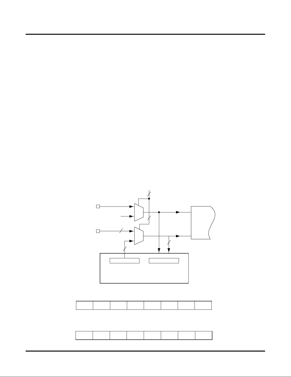
Lattice Semiconductor ispPAC-POWR1220AT8 Data Sheet
Writing a value to the ADC_MUX register to set the input attenuator and selector will automatically initiate a conversion. When the conversion is in process, the DONE bit (ADC_VALUE_LOW.0) will be reset to 0. When the conver-
sion is complete, this bit will be set to 1. When the conversion is complete, the result may be read out of the ADC by
performing two I2C read operations; one for ADC_VALUE_LOW, and one for ADC_VALUE_HIGH. It is recom-
mended that the I2C master load a second conversion command only after the completion of the current conversion
command (Waiting for the DONE bit to be set to 1). An alternative would be to wait for a minimum specified time
(see T
CONVERT
value in the specifications) and disregard checking the DONE bit.
Note that if the I2C clock rate falls below 50kHz (see F
conversion is to wait the minimum specified time (T
note in specifications), the only way to insure a valid ADC
I2C
CONVERT
), as the operation of the DONE bit at clock rates lower
than that cannot be guaranteed. In other words, if the I2C clock rate is less than 50kHz, the DONE bit may or may
not assert even though a valid conversion result is available.
To insure every ADC conversion result is valid, preferred operation is to clock I2C at more than 50kHz and verify
DONE bit status or wait for the full T
CONVERT
time period between subsequent ADC convert commands. If an I2C
request is placed before the current conversion is complete, the DONE bit will be set to 1 only after the second
request is complete.
The status of the digital input lines may also be monitored and controlled through I2C commands. Figure 25 shows
the I2C interface to the IN[1:6] digital input lines. The input status may be monitored by reading the INPUT_STATUS
register, while input values to the PLD array may be set by writing to the INPUT_VALUE register. To be able to set
an input value for the PLD array, the input multiplexer associated with that bit needs to be set to the I2C register setting in E2CMOS memory otherwise the PLD will receive its input from the INx pin.
Figure 25. I
2C Digital Input Interface
IN1
USERJTAG
IN[2..6]
PLD Output/Input_Value Register Select
Bit
5
5
(E2 Configuration)
6
MUX
5
MUX
PLD
Array
5
Input_Status Input_Value
2
C Interface Unit
I
0x06 - INPUT_STATUS
X X IN6IN5IN4IN3IN2IN1
b7 b0
0x11 - INPUT_VALUE (Read/Write)
XX
b7 b0
b6 b5 b4 b3 b2 b1
b6 b5 b4 b3 b2 b1
(Read Only)
I6 I5 I4 I3 I2 X
35

Lattice Semiconductor ispPAC-POWR1220AT8 Data Sheet
The digital outputs may also be monitored and controlled through the I2C interface, as shown in Figure 26. The status of any given digital output may be read by reading the contents of the associated OUTPUT_STATUS[2:0] register. Note that in the case of the outputs, the status reflected by these registers reflects the logic signal used to drive
the pin, and does not sample the actual level present on the output pin. For example, if an output is set high but is
not pulled up, the output status bit corresponding with that pin will read ‘1’, but a high output signal will not appear
on the pin.
Digital outputs may also be optionally controlled directly by the I2C bus instead of by the PLD array. The outputs
may be driven either from the PLD ORP or from the contents of the GP_OUTPUT[2:0] registers with the choice
user-settable in E2CMOS memory. Each output may be independently set to output from the PLD or from the
GP_OUTPUT registers.
36
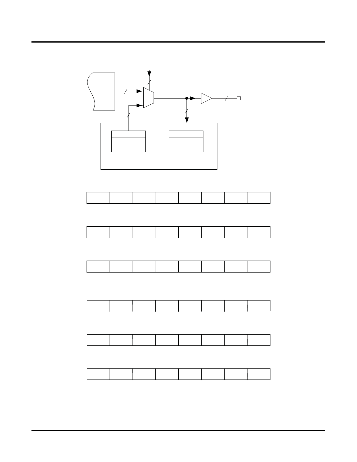
Lattice Semiconductor ispPAC-POWR1220AT8 Data Sheet
Figure 26. I
2C Output Monitor and Control Logic
PLD Output/GP_Output Register Select
PLD
Output
Routing
Pool
GP_Output1
GP_Output2
GP_Output3
0x03 - OUTPUT_STATUS0
OUT8 OUT7 OUT6 OUT5 HVOU T4 HVOUT3 HVOUT2 HVOUT1
b7 b0
0x04 - OUTPUT_STATUS1
2
(E
Configuration)
20
20
MUX
20
2
I
C Interface Unit
(Read Only)
b6 b5 b4 b3 b2 b1
(Read Only)
20
Output_Status0
Output_Status1
Output_Status2
20
HVOUT[1..4]
OUT[5..20]
OUT16 OUT15 OUT14 OUT13 OUT12 OUT11 OUT10 OUT9
b7 b0
0x05 - OUTPUT_STATUS2
X X X X OUT20 OUT19 OUT18 OUT17
b7 b0
b6 b5 b4 b3 b2 b1
(Read Only)
b6 b5 b4 b3 b2 b1
0x0E - GP_OUTPUT1 (Read/Write)
GP8 GP7 GP6 GP5_ENb GP4 GP3 GP2 GP1
b7 b0
b6 b5 b4 b3 b2 b1
0x0F - GP_OUTPUT2 (Read/Write)
GP16 GP15 GP14 GP13 GP12 GP11 GP10 GP9
b7 b0
b6 b5 b4 b3 b2 b1
0x10 - GP_OUTPUT3 (Read/Write)
X X X X GP20 GP19 GP18 GP17
b7 b0
b6 b5 b4 b3 b2 b1
The UES word may also be read through the I2C interface, with the register mapping shown in Figure 27.
37

Lattice Semiconductor ispPAC-POWR1220AT8 Data Sheet
Figure 27. I
2C Register Mapping for UES Bits
0x0A - UES_BYTE0
UES7 UES6 UES5 UES4 UES3 UES2 UES1 UES0
b7 b0
0x0B - UES_BYTE1
UES15 UES14 UES13 UES12 UES11 UES10 UES9 UES8
b7 b0
0x0C - UES_BYTE2
UES23 UES22 UES21 UES20 UES19 UES18 UES17 UES16
b7 b0
0x0D - UES_BYTE3
UES31 UES30 UES29 UES28 UES27 UES26 UES25 UES24
b7 b0
(Read Only)
b6 b5 b4 b3 b2 b1
(Read Only)
b6 b5 b4 b3 b2 b1
(Read Only)
b6 b5 b4 b3 b2 b1
(Read Only)
b6 b5 b4 b3 b2 b1
The I2C interface also provides the ability to initiate reset operations. The ispPAC-POWR1220AT8 may be reset by
issuing a write of any value to the I2C RESET register (Figure 28). Note: The execution of the I2C reset command is
equivalent to toggling the Resetb pin of the chip. Refer to the Resetb Signal, RESET Command via JTAG or I2C
section of this data sheet for further information.
Figure 28. I
2C Reset Register
0x12 - RESET (Write Only)
XXXXXXXX
b7 b0
b6 b5 b4 b3 b2 b1
38

Lattice Semiconductor ispPAC-POWR1220AT8 Data Sheet
The ispPAC-POWR1220AT8 also provides the user with the ability to program the trim values over the I2C interface,
by writing the appropriate binary word to the associated trim register (Figure 29).
Figure 29. I
2C Trim Registers
0x13 - TRIM1_TRIM (Read/Write)
D7 D6 D5 D4 D3 D2 D1 D0
b7 b0
0x14 - TRIM2_TRIM (Read/Write)
D7 D6 D5 D4 D3 D2 D1 D0
b7 b0
0x15 - TRIM3_TRIM (Read/Write)
D7 D6 D5 D4 D3 D2 D1 D0
b7 b0
0x16 - TRIM4_TRIM (Read/Write)
D7 D6 D5 D4 D3 D2 D1 D0
b7 b0
0x17 - TRIM5_TRIM (Read/Write)
b6 b5 b4 b3 b2 b1
b6 b5 b4 b3 b2 b1
b6 b5 b4 b3 b2 b1
b6 b5 b4 b3 b2 b1
D7 D6 D5 D4 D3 D2 D1 D0
b7 b0 b6 b5 b4 b3 b2 b1
0x18 - TRIM6_TRIM (Read/Write)
D7 D6 D5 D4 D3 D2 D1 D0
b7 b0
b6 b5 b4 b3 b2 b1
0x19 - TRIM7_TRIM (Read/Write)
D7 D6 D5 D4 D3 D2 D1 D0
b7 b0
b6 b5 b4 b3 b2 b1
0x1A - TRIM8_TRIM (Read/Write)
D7 D6 D5 D4 D3 D2 D1 D0
b7 b0
b6 b5 b4 b3 b2 b1
39
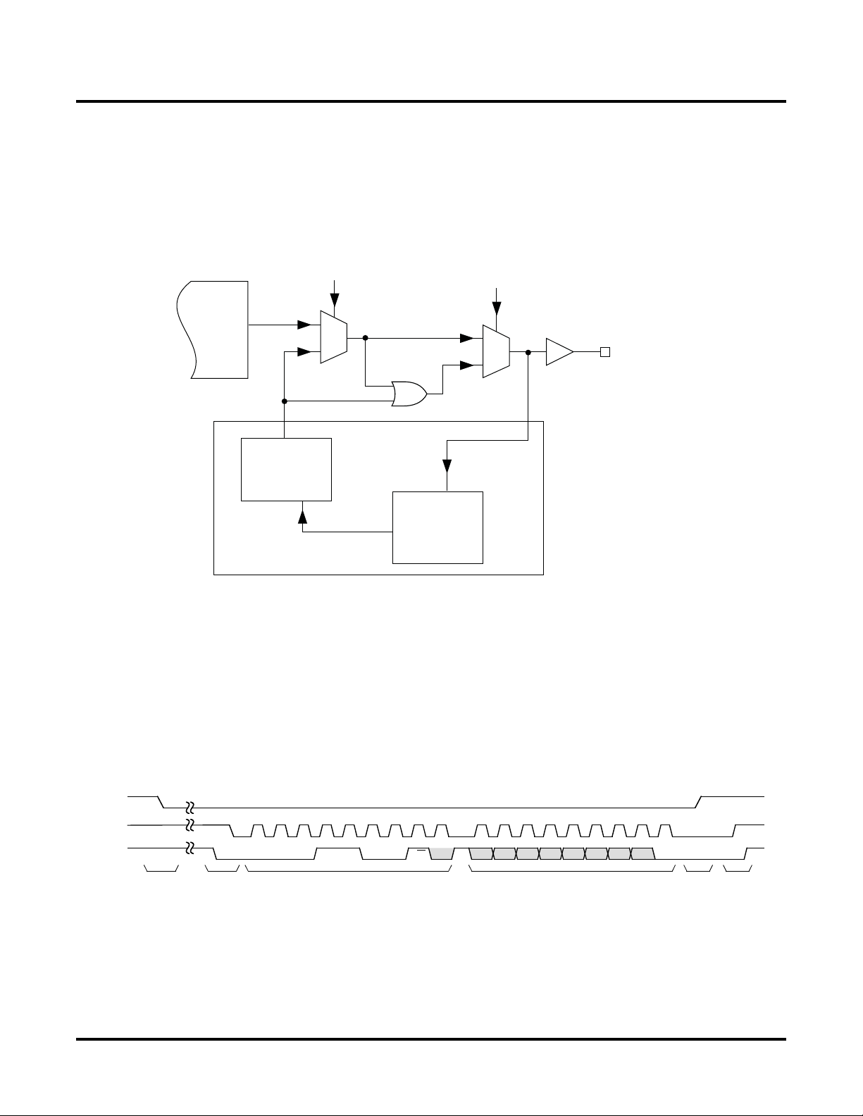
Lattice Semiconductor ispPAC-POWR1220AT8 Data Sheet
SMBus SMBAlert Function
The ispPAC-POWR1220AT8 provides an SMBus SMBAlert function so that it can request service from the bus
master when it is used as part of an SMBus system. This feature is supported as an alternate function of OUT5.
When the SMBAlert feature is enabled, OUT5 is controlled by a combination of the PLD ORP and the GP5_ENb bit
(Figure 30). Note: To enable the SMBAlert feature, the SMB_Mode (EECMOS bit) should be set in software.
Figure 30. ispPAC-POWR1220AT8 SMBAlert Logic
PLD Output/GP_Output Register Select
PLD
Output
Routing
Pool
(E2 Configuration)
MUX
OUT5/SMBA Mode Select
(E2 Configuration)
MUX
OUT5/SMBA
GP5_ENb
SMBAlert
Logic
I2C Interface Unit
The typical flow for an SMBAlert transaction is as follows (Figure 30):
1. GP5_ENb bit is forced (Via I2C write) to Low
2. ispPAC-POWR1220AT8 PLD Logic pulls OUT5/SMBA Low
3. Master responds to interrupt from SMBA line
4. Master broadcasts a read operation using the SMBus Alert Response Address (ARA)
5. ispPAC-POWR1220AT8 responds to read request by transmitting its device address
6. If transmitted device address matches ispPAC-POWR1220AT8 address, it sets GP5_ENb bit high.
This releases OUT5/SMBA.
Figure 31. SMBAlert Bus Transaction
SMBA
SCL
SDA
SLAVE
ASSERTS
SMBA
START
123456789
000110 0
ALERT RESPONSE ADDRESS
(0001 100)
R/W
ACK A4 A3 A2 A1 A0 xA5A6
123456789
ACK
SLAVE ADDRESS (7 BITS)
Note: Shaded Bits Asserted by Slave
SLAVE
RELEASES
SMBA
STOP
After OUT5/SMBA has been released, the bus master (typically a microcontroller) may opt to perform some service
functions in which it may send data to or read data from the ispPAC-POWR1220AT8. As part of the service functions, the bus master will typically need to clear whatever condition initiated the SMBAlert request, and will also
need to reset GP5_ENb to re-enable the SMBAlert function. For further information on the SMBus, the user should
consult the SMBus Standard.
40

Lattice Semiconductor ispPAC-POWR1220AT8 Data Sheet
Designs using the SMBAlert feature are required to set the device’s I2C/SMBus address to the lowest of all the
addresses on that I2C/SMBus.
Software-Based Design Environment
Designers can configure the ispPAC-POWR1220AT8 using PAC-Designer, an easy to use, Microsoft Windows
compatible program. Circuit designs are entered graphically and then verified, all within the PAC-Designer environment. Full device programming is supported using PC parallel port I/O operations and a download cable connected
to the serial programming interface pins of the ispPAC-POWR1220AT8. A library of configurations is included with
basic solutions and examples of advanced circuit techniques are available on the Lattice web site for downloading.
In addition, comprehensive on-line and printed documentation is provided that covers all aspects of PAC-Designer
operation. The PAC-Designer schematic window, shown in Figure 32, provides access to all configurable ispPACPOWR1220AT8 elements via its graphical user interface. All analog input and output pins are represented. Static
or non-configurable pins such as power, ground, and the serial digital interface are omitted for clarity. Any element
in the schematic window can be accessed via mouse operations as well as menu commands. When completed,
configurations can be saved, simulated, and downloaded to devices.
Figure 32. PAC-Designer ispPAC-POWR1220AT8 Design Entry Screen
In-System Programming
The ispPAC-POWR1220AT8 is an in-system programmable device. This is accomplished by integrating all E2 configuration memory and control logic on-chip. Programming is performed through a 4-wire, IEEE 1149.1 compliant
serial JTAG interface at normal logic levels. Once a device is programmed, all configuration information is stored
on-chip, in non-volatile E2CMOS memory cells. The specifics of the IEEE 1149.1 serial interface and all ispPACPOWR1220AT8 instructions are described in the JTAG interface section of this data sheet.
41

Lattice Semiconductor ispPAC-POWR1220AT8 Data Sheet
Programming ispPAC-POWR1220AT8: Alternate Method
Some applications require that the ispPAC-POWR1220AT8 be programmed before turning the power on to the
entire circuit board. To meet such application needs, the ispPAC-POWR1220AT8 provides an alternate programming method which enables the programming of the ispPAC-POWR1220AT8 device through the JTAG chain with a
separate power supply applied just to the programming section of the ispPAC-POWR1220AT8 device with the main
power supply of the board turned off.
Three special purpose pins, VCCPROG, ATDI and TDISEL, enable programming of the un-programmed ispPACPOWR1220AT8 under such circumstances. The VCCPROG pin powers just the programming circuitry of the ispPAC-POWR1220AT8 device. The ATDI pin provides an alternate connection to the JTAG header while bypassing
all the un-powered devices in the JTAG chain. TDISEL pin enables switching between the ATDI and the standard
JTAG signal TDI. When the internally pulled-up TDISEL = 1, standard TDI pin is enabled and when the TDISEL = 0,
ATDI is enabled.
In order to use this feature the JTAG signals of the ispPAC-POWR1220AT8 are connected to the header as shown
in figure 32. Note: The ispPAC-POWR1220AT8 should be the last device in the JTAG chain.
Figure 33. ispPAC-POWR1220AT8 Alternate TDI Configuration Diagram
1. Power for
3. Sequenced Power
Supply Turn-on
VCCIO
VCCJ
VCC
2. Initial Power
Supply Turn-On
Programming
POWR1220AT8
VCCJ
VCC
VCCPROG
JTAG Signal
TDI
TCK
TMS
TDO
TDISEL
Connector
TDI
Other JTAG
Device(s)
TCK
TMS
TDO
TDI
ATDI
ispPAC-POWR
1220AT8
TCK
TMS
TDISEL
TDO
Alternate TDI Selection Via JTAG Command
When the TDISEL pin held high and four consecutive IDCODE instructions are issued, ispPAC-POWR1220AT8
responds by making its active JTAG data input the ATDI pin. When ATDI is selected, data on its TDI pin is ignored
until the JTAG state machine returns to the Test-Logic-Reset state.
This method of selecting ATDI takes advantage of the fact that a JTAG device with an IDCODE register will automatically load its unique IDCODE instruction into the Instruction Register after a Test-Logic-Reset. This JTAG capability permits blind interrogation of devices so that their location in a serial chain can be identified without having to
know anything about them in advance. A blind interrogation can be made using only the TMS and TCLK control
pins, which means TDI and TDO are not required for performing the operation. Figure 34 illustrates the logic for
selecting whether the TDI or ATDI pin is the active data input to ispPAC-POWR1220AT8.
42

Lattice Semiconductor ispPAC-POWR1220AT8 Data Sheet
Figure 34. ispPAC-POWR1220AT8 TDI/ATDI Pin Selection Diagram
TMS TCK
TDI
ATDI
TDISEL
1
0
Test-Logic-Reset
JTAG
SET
Q
CLR
ispPAC-POWR1220AT8
IDCODE Instructions
Loaded at Update-IR
TDO
4 Consecutive
Table 12 shows in truth table form the same conditions required to select either TDI or ATDI as in the logic diagram
found in Figure 34.
Table 12. ispPAC-POWR1220AT8 ATDI/TDI Selection Table
TDISEL Pin
H No Yes ATDI (TDI Disabled)
HYesNo TDI (ATDI Disabled)
L X X ATDI (TDI Disabled)
JTAG State Machine
Test-Logic-Reset
4 Consecutive
IDCODE Commands
Loaded at Update-IR
Active JTAG
Data Input Pin
Please refer to the Lattice application note AN6068, Programming the ispPAC-POWR1220AT8 in a JTAG Chain
Using ATDI. The application note includes specific SVF code examples and information on the use of Lattice
design tools to verify device operation in alternate TDI mode.
VCCPROG Power Supply Pin
Because the VCCPROG pin directly powers the on-chip programming circuitry, the ispPAC-POWR1220AT8 device
can be programmed by applying power to the VCCPROG pin (without powering the entire chip though the VCCD
and VCCA pins). In addition, to enable the on-chip JTAG interface circuitry, power should be applied to the VCCJ
pin.
When the ispPAC-POWR1220AT8 is using the VCCPROG pin, its VCCD and VCCA pins can be open or pulled low.
Additionally, other than JTAG I/O pins, all digital output pins are in Hi-Z state, HVOUT pins configured as MOSFET
driver are driven low, and all other inputs are ignored.
To switch the power supply back to VCCD and VCCA pins, one should turn the VCCPROG supply and VCCJ off
before turning the regular supplies on.
User Electronic Signature
A user electronic signature (UES) feature is included in the E2CMOS memory of the ispPAC-POWR1220AT8. This
consists of 32 bits that can be configured by the user to store unique data such as ID codes, revision numbers or
43

Lattice Semiconductor ispPAC-POWR1220AT8 Data Sheet
inventory control data. The specifics of this feature are discussed in the IEEE 1149.1 serial interface section of this
data sheet.
Electronic Security
An electronic security “fuse” (ESF) bit is provided in every ispPAC-POWR1220AT8 device to prevent unauthorized
readout of the E
2
CMOS configuration bit patterns. Once programmed, this cell prevents further access to the functional user bits in the device. This cell can only be erased by reprogramming the device, so the original configuration cannot be examined once programmed. Usage of this feature is optional. The specifics of this feature are
discussed in the IEEE 1149.1 serial interface section of this data sheet.
Production Programming Support
Once a final configuration is determined, an ASCII format JEDEC file can be created using the PAC-Designer software. Devices can then be ordered through the usual supply channels with the user’s specific configuration already
preloaded into the devices. By virtue of its standard interface, compatibility is maintained with existing production
programming equipment, giving customers a wide degree of freedom and flexibility in production planning.
Evaluation Fixture
Included in the basic ispPAC-POWR1220AT8 Design Kit is an engineering prototype board that can be connected
to the parallel port of a PC using a Lattice download cable. It demonstrates proper layout techniques for the ispPAC-POWR1220AT8 and can be used in real time to check circuit operation as part of the design process. Input
and output connections are provided to aid in the evaluation of the ispPAC-POWR1220AT8 for a given application.
(Figure 35).
Figure 35. Download from a PC
PAC-Designer
Software
Other
System
Circuitry
ispDOWNLOAD
Cable (6')
4
ispPAC-POWR
1220AT8
Device
IEEE Standard 1149.1 Interface (JTAG)
Serial Port Programming Interface Communication with the ispPAC-POWR1220AT8 is facilitated via an IEEE
1149.1 test access port (TAP). It is used by the ispPAC-POWR1220AT8 as a serial programming interface. A brief
description of the ispPAC-POWR1220AT8 JTAG interface follows. For complete details of the reference specification, refer to the publication, Standard Test Access Port and Boundary-Scan Architecture, IEEE Std 1149.1-1990
(which now includes IEEE Std 1149.1a-1993).
Overview
An IEEE 1149.1 test access port (TAP) provides the control interface for serially accessing the digital I/O of the ispPAC-POWR1220AT8. The TAP controller is a state machine driven with mode and clock inputs. Given in the correct
sequence, instructions are shifted into an instruction register, which then determines subsequent data input, data
output, and related operations. Device programming is performed by addressing the configuration register, shifting
data in, and then executing a program configuration instruction, after which the data is transferred to internal
E2CMOS cells. It is these non-volatile cells that store the configuration or the ispPAC-POWR1220AT8. A set of
instructions are defined that access all data registers and perform other internal control operations. For compatibil-
44

Lattice Semiconductor ispPAC-POWR1220AT8 Data Sheet
ity between compliant devices, two data registers are mandated by the IEEE 1149.1 specification. Others are functionally specified, but inclusion is strictly optional. Finally, there are provisions for optional data registers defined by
the manufacturer. The two required registers are the bypass and boundary-scan registers. Figure 36 shows how
the instruction and various data registers are organized in an ispPAC-POWR1220AT8.
Figure 36. ispPAC-POWR1220AT8 TAP Registers
MULTIPLEXER
DATA REGISTER (243 BITS)
ADDRESS REGISTER (169 BITS)
UES REGISTER (32 BITS)
IDCODE REGISTER (32 BITS)
CFG ADDRESS REGISTER (12 BITS)
CFG DATA REGISTER (156 BITS)
BYPASS REGISTER (1 BIT)
INSTRUCTION REGISTER (8 BITS)
TEST ACCESS PORT (TAP)
LOGIC
E2CMOS
NON-VOLATILE
MEMORY
OUTPUT
LATCH
TDI
TCK TMS TDO
TAP Controller Specifics
The TAP is controlled by the Test Clock (TCK) and Test Mode Select (TMS) inputs. These inputs determine whether
an Instruction Register or Data Register operation is performed. Driven by the TCK input, the TAP consists of a
small 16-state controller design. In a given state, the controller responds according to the level on the TMS input as
shown in Figure 37. Test Data In (TDI) and TMS are latched on the rising edge of TCK, with Test Data Out (TDO)
becoming valid on the falling edge of TCK. There are six steady states within the controller: Test-Logic-Reset, RunTest/Idle, Shift-Data-Register, Pause-Data-Register, Shift-Instruction-Register and Pause-Instruction-Register. But
there is only one steady state for the condition when TMS is set high: the Test-Logic-Reset state. This allows a
reset of the test logic within five TCKs or less by keeping the TMS input high. Test-Logic-Reset is the power-on
default state.
45

Lattice Semiconductor ispPAC-POWR1220AT8 Data Sheet
Figure 37. TAP States
Test-Logic-Rst
1
Run-Test/Idle
0
0
11 1
Select-DR-Scan Select-IR-Scan
11
00
00
Capture-DR Capture-IR
00
Shift-DR Shift-IR
11
Exit1-DR Exit1-IR
00
Pause-DR Pause-IR
11
Exit2-DR Exit2-IR
11
Update-DR Update-IR
00
11
00
0011
Note: The value shown adjacent to each state transition in this figure
represents the signal present at TMS at the time of a rising edge at TCK.
When the correct logic sequence is applied to the TMS and TCK inputs, the TAP will exit the Test-Logic-Reset state
and move to the desired state. The next state after Test-Logic-Reset is Run-Test/Idle. Until a data or instruction shift
is performed, no action will occur in Run-Test/Idle (steady state = idle). After Run-Test/Idle, either a data or instruction shift is performed. The states of the Data and Instruction Register blocks are identical to each other differing
only in their entry points. When either block is entered, the first action is a capture operation. For the Data Registers, the Capture-DR state is very simple: it captures (parallel loads) data onto the selected serial data path (previously chosen with the appropriate instruction). For the Instruction Register, the Capture-IR state will always load
the IDCODE instruction. It will always enable the ID Register for readout if no other instruction is loaded prior to a
Shift-DR operation. This, in conjunction with mandated bit codes, allows a “blind” interrogation of any device in a
compliant IEEE 1149.1 serial chain. From the Capture state, the TAP transitions to either the Shift or Exit1 state.
Normally the Shift state follows the Capture state so that test data or status information can be shifted out or new
data shifted in. Following the Shift state, the TAP either returns to the Run-Test/Idle state via the Exit1 and Update
states or enters the Pause state via Exit1. The Pause state is used to temporarily suspend the shifting of data
through either the Data or Instruction Register while an external operation is performed. From the Pause state,
shifting can resume by reentering the Shift state via the Exit2 state or be terminated by entering the Run-Test/Idle
state via the Exit2 and Update states. If the proper instruction is shifted in during a Shift-IR operation, the next entry
into Run-Test/Idle initiates the test mode (steady state = test). This is when the device is actually programmed,
erased or verified. All other instructions are executed in the Update state.
Test Instructions
Like data registers, the IEEE 1149.1 standard also mandates the inclusion of certain instructions. It outlines the
function of three required and six optional instructions. Any additional instructions are left exclusively for the manufacturer to determine. The instruction word length is not mandated other than to be a minimum of two bits, with only
the BYPASS and EXTEST instruction code patterns being specifically called out (all ones and all zeroes respectively). The ispPAC-POWR1220AT8 contains the required minimum instruction set as well as one from the optional
instruction set. In addition, there are several proprietary instructions that allow the device to be configured and ver-
46

Lattice Semiconductor ispPAC-POWR1220AT8 Data Sheet
ified. Table 13 lists the instructions supported by the ispPAC-POWR1220AT8 JTAG Test Access Port (TAP) controller:
Table 13. ispPAC-POWR1220AT8 TAP Instruction Table
Instruction
Code Comments
BULK_ERASE 0000 0011 Bulk erase device
BYPASS 1111 1111 Bypass - connect TDO to TDI
DISCHARGE 0001 0100 Fast VPP discharge
ERASE_DONE_BIT 0010 0100 Erases ‘Done’ bit only
EXTEST 0000 0000 Bypass - connect TDO to TDI
IDCODE 0001 0110 Read contents of manufacturer ID code (32 bits)
OUTPUTS_HIGHZ 0001 1000 Force all outputs to High-Z state, FET outputs pulled low
SAMPLE/PRELOAD 00011100 Sample/Preload. Default to bypass.
PROGRAM_DISABLE 0001 1110 Disable program mode
PROGRAM_DONE_BIT 0010 1111 Programs the Done bit
PROGRAM_ENABLE 0001 0101 Enable program mode
PROGRAM_SECURITY 0000 1001 Program security fuse
Command
RESET 0010 0010
Resets device (refer to the RESETb Signal, RESET Command via
JTAG or I
2
C section of this data sheet)
IN1_RESET_JTAG_BIT 0001 0010 Reset the JTAG bit associated with IN1 pin to 0
IN1_SET_JTAG_BIT 0001 0011 Set the JTAG bit associated with IN1 pin to 1
CFG_ADDRESS 0010 1011 Select non-PLD address register
CFG_DATA_SHIFT 0010 1101 Non-PLD data shift
CFG_ERASE 0010 1001 ERASE Just the Non PLD configuration
CFG_PROGRAM 0010 1110 Non-PLD program
CFG_VERIFY 0010 1000 VRIFY non-PLD fusemap data
PLD_ADDRESS_SHIFT 0000 0001 PLD_Address register (169 bits)
PLD_DATA_SHIFT 0000 0010 PLD_Data register (243 Bits)
PLD_INIT_ADDR_FOR_PROG_INCR 0010 0001 Initialize the address register for auto increment
2
PLD_PROG_INCR 0010 0111 Program column register to E
PLD_PROGRAM 0000 0111 Program PLD data register to E
and auto increment address register
2
PLD_VERIFY 0000 1010 Verifies PLD column data
2
PLD_VERIFY_INCR 0010 1010 Load column register from E
UES_PROGRAM 0001 1010 Program UES bits into E
and auto increment address register
2
UES_READ 0001 0111 Read contents of UES register from E2 (32 bits)
BYPASS is one of the three required instructions. It selects the Bypass Register to be connected between TDI and
TDO and allows serial data to be transferred through the device without affecting the operation of the ispPACPOWR1220AT8. The IEEE 1149.1 standard defines the bit code of this instruction to be all ones (11111111).
The required SAMPLE/PRELOAD instruction dictates the Boundary-Scan Register be connected between TDI
and TDO. The ispPAC-POWR1220AT8 has no boundary scan register, so for compatibility it defaults to the
BYPASS mode whenever this instruction is received. The bit code for this instruction is defined by Lattice as shown
in Table 13.
The EXTEST (external test) instruction is required and would normally place the device into an external boundary
test mode while also enabling the boundary scan register to be connected between TDI and TDO. Again, since the
47

Lattice Semiconductor ispPAC-POWR1220AT8 Data Sheet
ispPAC-POWR1220AT8 has no boundary scan logic, the device is put in the BYPASS mode to ensure specification
compatibility. The bit code of this instruction is defined by the 1149.1 standard to be all zeros (00000000).
The optional IDCODE (identification code) instruction is incorporated in the ispPAC-POWR1220AT8 and leaves it in
its functional mode when executed. It selects the Device Identification Register to be connected between TDI and
TDO. The Identification Register is a 32-bit shift register containing information regarding the IC manufacturer,
device type and version code (Figure 38). Access to the Identification Register is immediately available, via a TAP
data scan operation, after power-up of the device, or by issuing a Test-Logic-Reset instruction. The bit code for this
instruction is defined by Lattice as shown in Table 13.
Figure 38. ispPAC-POWR1220AT8 ID Code
MSB LSB
XXXX / 0000 0001 0100 0100 / 0000 0100 001 / 1
Part Number
0144h = ispPAC-POWR1220AT8
Version
(4 bits)
2
E
Configured
(16 bits)
JEDEC Manufacturer
Identity Code for
Lattice Semiconductor
(11 bits)
per 1149.1-1990
Constant 1
(1 bit)
ispPAC-POWR1220AT8 Specific Instructions
There are 25 unique instructions specified by Lattice for the ispPAC-POWR1220AT8. These instructions are primarily used to interface to the various user registers and the E2CMOS non-volatile memory. Additional instructions are
used to control or monitor other features of the device. A brief description of each unique instruction is provided in
detail below, and the bit codes are found in Table 13.
PLD_ADDRESS_SHIFT – This instruction is used to set the address of the PLD AND/ARCH arrays for subsequent
program or read operations. This instruction also forces the outputs into the OUTPUTS_HIGHZ.
PLD_DATA_SHIFT – This instruction is used to shift PLD data into the register prior to programming or reading.
This instruction also forces the outputs into the OUTPUTS_HIGHZ.
PLD_INIT_ADDR_FOR_PROG_INCR – This instruction prepares the PLD address register for subsequent
PLD_PROG_INCR or PLD_VERIFY_INCR instructions.
PLD_PROG_INCR – This instruction programs the PLD data register for the current address and increments the
address register for the next set of data.
PLD_PROGRAM – This instruction programs the selected PLD AND/ARCH array column. The specific column is
preselected by using PLD_ADDRESS_SHIFT instruction. The programming occurs at the second rising edge of
the TCK in Run-Test-Idle JTAG state. The device must already be in programming mode (PROGRAM_ENABLE
instruction). This instruction also forces the outputs into the OUTPUTS_HIGHZ.
PROGRAM_SECURITY – This instruction is used to program the electronic security fuse (ESF) bit. Programming
the ESF bit protects proprietary designs from being read out. The programming occurs at the second rising edge of
the TCK in Run-Test-Idle JTAG state. The device must already be in programming mode (PROGRAM_ENABLE
instruction). This instruction also forces the outputs into the OUTPUTS_HIGHZ.
PLD_VERIFY – This instruction is used to read the content of the selected PLD AND/ARCH array column. This
specific column is preselected by using PLD_ADDRESS_SHIFT instruction. This instruction also forces the outputs
into the OUTPUTS_HIGHZ.
48

Lattice Semiconductor ispPAC-POWR1220AT8 Data Sheet
DISCHARGE – This instruction is used to discharge the internal programming supply voltage after an erase or pro-
gramming cycle and prepares ispPAC-POWR1220AT8 for a read cycle. This instruction also forces the outputs into
the OUTPUTS_HIGHZ.
CFG_ADDRESS – This instruction is used to set the address of the CFG array for subsequent program or read
operations. This instruction also forces the outputs into the OUTPUTS_HIGHZ.
CFG_DATA_SHIFT – This instruction is used to shift data into the CFG register prior to programming or reading.
This instruction also forces the outputs into the OUTPUTS_HIGHZ.
CFG_ERASE – This instruction will bulk erase the CFG array. The action occurs at the second rising edge of TCK
in Run-Test-Idle JTAG state. The device must already be in programming mode (PROGRAM_ENABLE instruction).
This instruction also forces the outputs into the OUTPUTS_HIGHZ.
CFG_PROGRAM – This instruction programs the selected CFG array column. This specific column is preselected
by using CFG_ADDRESS instruction. The programming occurs at the second rising edge of the TCK in Run-TestIdle JTAG state. The device must already be in programming mode (PROGRAM_ENABLE instruction). This
instruction also forces the outputs into the OUTPUTS_HIGHZ.
CFG_VERIFY – This instruction is used to read the content of the selected CFG array column. This specific column
is preselected by using CFG_ADDRESS instruction. This instruction also forces the outputs into the
OUTPUTS_HIGHZ.
BULK_ERASE – This instruction will bulk erase all E
2
CMOS bits (CFG, PLD, UES, and ESF) in the ispPACPOWR1220AT8. The device must already be in programming mode (PROGRAM_ENABLE instruction). This
instruction also forces the outputs into the OUTPUTS_HIGHZ.
OUTPUTS_HIGHZ – This instruction turns off all of the open-drain output transistors. Pins that are programmed as
FET drivers will be placed in the active low state. This instruction is effective after Update-Instruction-Register
JTAG state.
PROGRAM_ENABLE – This instruction enables the programming mode of the ispPAC-POWR1220AT8. This
instruction also forces the outputs into the OUTPUTS_HIGHZ.
IDCODE – This instruction connects the output of the Identification Code Data Shift (IDCODE) Register to TDO
(Figure 39), to support reading out the identification code.
Figure 39. IDCODE Register
Bit
31
Bit
30
Bit
29
Bit
28
Bit
27
Bit
Bit
4
3
Bit
2
Bit
1
Bit
TDO
0
PROGRAM_DISABLE – This instruction disables the programming mode of the ispPAC-POWR1220AT8. The TestLogic-Reset JTAG state can also be used to cancel the programming mode of the ispPAC-POWR1220AT8.
UES_READ – This instruction both reads the E
2
CMOS bits into the UES register and places the UES register
between the TDI and TDO pins (as shown in Figure 40), to support programming or reading of the user electronic
signature bits.
Figure 40. UES Register
Bit
Bit
Bit
15
13
14
Bit
12
10
11
8
9
6
7
4
5
2
3
0
1
TDO
Bit
Bit
Bit
Bit
Bit
Bit
Bit
Bit
Bit
Bit
Bit
Bit
49

Lattice Semiconductor ispPAC-POWR1220AT8 Data Sheet
UES_PROGRAM – This instruction will program the content of the UES Register into the UES E2CMOS memory.
The device must already be in programming mode (PROGRAM_ENABLE instruction). This instruction also forces
the outputs into the OUTPUTS_HIGHZ.
ERASE_DONE_BIT – This instruction clears the 'Done' bit, which prevents the ispPAC-POWR1220AT8 sequence
from starting.
PROGRAM_DONE_BIT – This instruction sets the 'Done' bit, which enables the ispPAC-POWR1220AT8
sequence to start.
RESET – This instruction resets the PLD sequence and output macrocells.
IN1_RESET_JTAG_BIT – This instruction clears the JTAG Register logic input 'IN1.' The PLD input has to be con-
figured to take input from the JTAG Register in order for this command to have effect on the sequence.
IN1_SET_JTAG_BIT – This instruction sets the JTAG Register logic input 'IN1.' The PLD input has to be configured
to take input from the JTAG Register in order for this command to have effect on the sequence.
PLD_VERIFY_INCR – This instruction reads out the PLD data register for the current address and increments the
address register for the next read.
Notes:
In all of the descriptions above, OUTPUTS_HIGHZ refers both to the instruction and the state of the digital output
pins, in which the open-drains are tri-stated and the FET drivers are pulled low.
Before any of the above programming instructions are executed, the respective E2CMOS bits need to be erased
using the corresponding erase instruction.
50
Lattice Semiconductor ispPAC-POWR1220AT8 Data Sheet
Package Diagrams
100-Pin TQFP
PIN 1 INDICATOR
D
3
A
e
8
D
3
TOP VIEW
SIDE VIEW
0.20 CMDA-B
c
SECTION B-B
b
b
c
1
b
1
SEATING PLANE
LEAD FINISH
BASE METAL
NOTES:
1. DIMENSIONING AND TOLERANCING PER ANSI Y14.5 - 1982.
2. ALL DIMENSIONS ARE IN MILLIMETERS.
DATUMS A, B AND D TO BE DETERMINED AT DATUM PLANE H.
3.
4. DIMENSIONS D1 AND E1 DO NOT INCLUDE MOLD PROTRUSION.
ALLOWABLE MOLD PROTRUSION IS 0.254 MM ON D1 AND E1
DIMENSIONS.
5. THE TOP OF PACKAGE MAY BE SMALLER THAN THE BOTTOM
OF THE PACKAGE BY 0.15 MM.
6. SECTION B-B:
THESE DIMENSIONS APPLY TO THE FLAT SECTION OF THE
LEAD BETWEEN 0.10 AND 0.25 MM FROM THE LEAD TIP.
7. A1 IS DEFINED AS THE DISTANCE FROM THE SEATING PLANE
TO THE LOWEST POINT ON THE PACKAGE BODY.
EXACT SHAPE OF EACH CORNER IS OPTIONAL.
8.
0.20 A-BC D 100X
E
E1
B
3
0.204X A-BHD
SEE DETAIL 'A'
C
0.10 C
DETAIL 'A'
A A2
D1
BOTTOM VIEW
H
0.20 MIN.
A1
1.00 REF.
SYMBOL
A--
A1
D
D1
E
E1
L
N
e
b1
MIN.
0.05
1.35A2
16.00 BSC
14.00 BSC
16.00 BSC
14.00 BSC
0.45
0.50 BSC
0.17b
0.17
0.09c
GAUGE PLANE
B
B
0-7
L
NOM.
-
1.40
0.60 0.75
100
0.22 0.27
0.20
0.15
MAX.
1.60
0.15
1.45
0.23
0.20
0.160.130.09c1
0.25
51

Lattice Semiconductor ispPAC-POWR1220AT8 Data Sheet
Part Number Description
Device Family
Device Number
ispPAC-POWR1220AT8 - 01XX100X
ispPAC-POWR1220AT8 Ordering Information
Conventional Packaging
Part Number Package Pins
ispPAC-POWR1220AT8-01T100I TQFP 100
Lead-Free Packaging
Part Number Package Pins
ispPAC-POWR1220AT8-01TN100I Lead-Free TQFP 100
Operating Temperature Range
I = Industrial (-40oC to +85oC)
Package
T = 100-pin TQFP
TN = Lead-Free 100-pin TQFP*
Performance Grade
01 = Standard
52
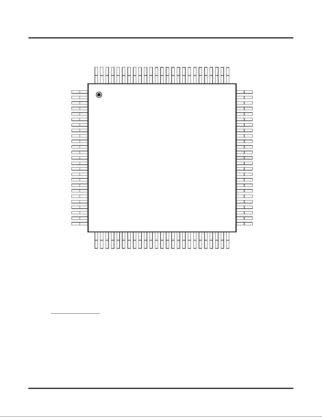
Lattice Semiconductor ispPAC-POWR1220AT8 Data Sheet
Package Options
NC
NC
1 N I
GNDD
K L C M
C D L P LK
CDC V
T2
2 M I R T
1 M I R
A D N G
U O V
U O V H T1
VPS1
VPS0
DDN G
H
L C S
A D
RESETb
S
3
M I
R T
T
NC
4 M I R T
5 M I R T
NCNCNC
IN2
IN3
GNDD
IN4
VCCINP
IN5
IN6
OUT5_SMBA
OUT6
OUT7
OUT8
OUT9
VCCD
OUT10
OUT11
OUT12
OUT13
OUT14
OUT15
OUT16
OUT17
GNDD
OUT18
OUT19
OUT20
1
2
3
4
5
6
7
8
9
10
11
12
13
14
15
16
17
18
19
20
21
22
23
24
25
9 9
0 0 1
6 9
8 9
7 9
5 9
2 9
4 9
3 9
9 8
1 9
0 9
6 8
8 8
5 8
7 8
ispPAC-POWR1220AT8
100-Pin TQFP
7 2
8
6 2
0 3 1 3
9 2
2
3 3
4 3 5 3 6 3
2
3
7 3
0 4
8 3
9
1 4 2 4
3
2 8
4 8
3 8
1 8
5
3 4 4 4
4
8 7
0 8
9 7
7 7
6 7
75
74
73
72
71
70
69
68
67
66
65
64
63
62
61
60
59
58
57
56
55
54
53
52
51
8 4
6 4
9
7
4
0
4
5
TRIM6
TRIM7
TRIM8
VMON12
VMON12GS
VMON11
VMON11GS
VMON10
VMON10GS
VMON9
VMON9GS
VMON8
VMON8GS
VMON7
VMON7GS
VCCA
RESERVED
VMON6
VMON6GS
VMON5
VMON5GS
VMON4
VMON4GS
VMON3
VMON3GS
I
NC
NC
S
M
T
NC
I D T
D T
A
Technical Support Assistance
Hotline: 1-800-LATTICE (North America)
+1-503-268-8001 (Outside North America)
e-mail: isppacs@latticesemi.com
Internet: www.latticesemi.com
J
L E
O D
C
S
C V
T
I D T
NC
K C
DDN
T
G
CD
C
V
4 T
3
G O R P C C V
NC
U O V
H
T
U O V
H
D E
V
R E S
GNDD
E
R
1 N O M V
S
A D N G
G 1 N O
M V
2 N O M V
S
G
NC
2
N O M V
53

Lattice Semiconductor ispPAC-POWR1220AT8 Data Sheet
Revision History
Date Version Change Summary
October 2005 1.0 Initial release.
March 2006 1.1
Correction for I
May 2006 1.2 Updated HVOUT Isource range:12.5µA to 100µA.
ADC Characteristics table, ADC Conversion Time: added entry for Tconvert = 200 µs.
Added footnotes for I
Figure 13, Isource 12.5µA to 100µA.
Clarified operation of ADC conversions.
October 2006 1.3 Data sheet status changed to “final”.
Analog Specifications table, lowered Max. Icc to 40 mA.
Voltage Monitors table, tightened Input Resistor Variation to 15%.
Digital Specifications table, included V
August 2007 01.4 Changes to HVOUT pin specifications.
Pin Descriptions table, note 4: Clarification for un-used VMON pins to be tied to
GNDD.
2
C/ADC calculation.
2
C frequency.
TAP instructions, added JTAG SAMPLE/PRELOAD instruction and notes for all JTAG
instructions
Margin Trim DAC Output Characteristics table, increased Max. DAC output current to
+/- 200 µA.
AC/Transient Characteristics table, tightened Internal Oscillator frequency variation
down to 5%.
and VIH specifications for I2C interface.
IL
54
 Loading...