

Page 1
ispClock5620A Evaluation Board:
ispPAC-CLK5620A-EV1
March 2007 Application Note AN6072
Introduction
The Lattice Semiconductor ispClock™5620A In-System-Programmable Analog Circuit allows designers to implement clock distribution networks supporting multiple, synchronized output frequencies using a single integrated circuit.
By integrating a Phase-Locked Loop (PLL) along with multiple output dividers, the ispClock5620A can derive up to
five separate output frequencies from a single input reference frequency. To facilitate the implementation of widefanout clock trees, the ispClock5620A provides up to 20 single-ended outputs or 10 differential outputs, organized
as ten banks of two. Each output bank may be independently programmed to support different logic standards and
operating options. Additionally, each single-ended output or differential output may be skew-adjusted to compensate for the effects of propagation delay along the PCB traces used in the distribution network. All configuration
data is stored internally in E
an industry-standard JTAG IEEE 1149.1 interface.
2
CMOS
®
non-volatile memory. Programming a configuration is accomplished through
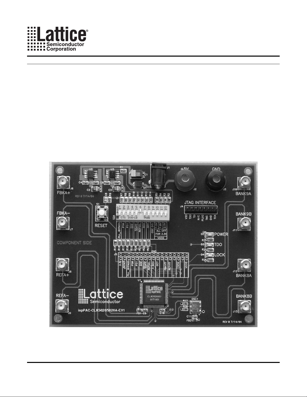
Figure 1. ispPAC-CLK5620A-EV1 Evaluation Board
ispPAC-CLK5620A-EV1 Evaluation Board
The ispPAC-CLK5620A-EV1 evaluation board (Figure 1) allows the designer to quickly configure and evaluate the
ispClock5620A on a fully assembled printed-circuit board. The four-layer board supports a 100-pin TQFP package,
© 2007 Lattice Semiconductor Corp. All Lattice trademarks, registered trademarks, patents, and disclaimers are as listed at www.latticesemi.com/legal. All other brand
or product names are trademarks or registered trademarks of their respective holders. The specifications and information herein are subject to change without notice.
www.latticesemi.com
1
an6072_01.1
Page 2

ispClock5620A Evaluation Board:
Lattice Semiconductor ispPAC-CLK5620A-EV1
a header for user I/O and a JTAG programming cable connector. SMA connectors are installed to provide high-signal integrity access to selected high-speed I/O signals. JTAG programming signals can be generated by using an
ispDOWNLOAD
user-programmable features of the ispPAC-CLK5620A can be easily configured using Lattice Semiconductor’s
PAC-Designer
®
programming cable connected between the evaluation board and a PC’s parallel (printer) port. All
®
software.
Programming Interface
Lattice Semiconductor’s ispDOWNLOAD cable can be used to program the ispClock5620A which is provided on
the evaluation board. This cable plugs into a PC-compatible’s parallel port connector, and includes active buffer circuitry inside its DB-25 connector housing. The other end of the ispDOWNLOAD cable terminates in an 8-pin 0.100”
pitch header connector which plugs directly into a mating connector provided on the ispPAC-CLK5620A-EV1 evaluation board.
Power Supply Considerations
The ispClock5620A operates with analog and digital core power supplies of 3.3V, while each output driver has a
dedicated power supply pin which may be driven with supply voltage of 1.5V, 1.8V, 2.5V or 3.3V, depending on the
logic standard which it has been configured to drive.
To simplify evaluation work, the ispPAC-CLK5620A-EV1 board was designed to operate from a single 4.5V-5.5V
power supply, which may be brought in through either a pair of banana plugs (J2 and J3), or a standard 5mm power
plug (J1 - center tip positive). The evaluation board provides two linear regulators to provide the appropriate operating voltages for the ispClock5620A. One of these regulators provides a fixed 3.3V for the analog and core functions, while the other regulator is dipswitch-programmable to provide 1.5V, 1.8V, 2.5V and 3.3V to power the
BANK8 and BANK9 output drivers.
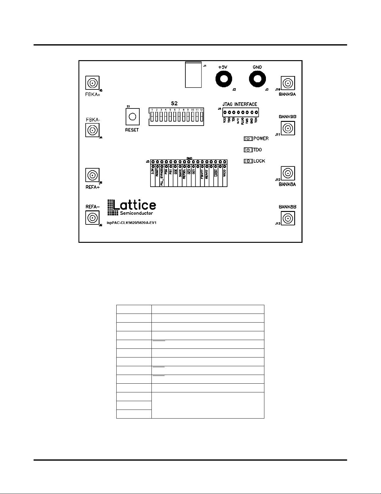
Input/Output Connections
Connectors are provided for key functions and test points on this evaluation board, as shown In Figure 2. Power
may be supplied in one of two ways; either through two color coded (RED = +, BLACK = -) banana jacks in the
upper right corner of the board or through a 5mm (center pin +) DC power connector (J1), The JTAG programming
cable is connected to a keyed header (J4) in the upper right corner of the board.
Access to a subset of the ispClock5620A’s I/O pins is available at J5, which is a 2x17 row of pads to which one may
attach test probes or a ribbon-cable connector. At this point most of the device’s non-RF control pins (except those
required for the JTAG programming interface) are accessible.
SMA connectors are provided along the left and right edges of the board to support access to key high-speed I/O
pins. Pairs of connectors are provided for the BANK8 and BANK9 outputs (J10-J13). Additional pairs of connectors
are provided for REFA(+/-) clock reference inputs (J8, J9) and FBKA (+, -) external feedback inputs (J6, J7). On this
evaluation board design the REFB(+/-) clock inputs are dedicated to supporting an on-board crystal oscillator.
Because this board was designed to maintain high levels of signal integrity at the edge rates at which the
ispClock5620A operates, it is strongly suggested that the user do not attempt to access any of the device’s highspeed I/O except through the provided SMA connectors and supporting impedance-controlled printed-circuit
traces.
2
Page 3
3
ispClock5620A Evaluation Board:
Lattice Semiconductor ispPAC-CLK5620A-EV1
Figure 2. I/O Connections, Controls and Indicators
Controls and Indicators
A 12-position dipswitch (S2) is provided on the evaluation board (Figure 2) for the purpose of setting device inputs
and programming the VCCO power supply for the BANK8 and BANK9 outputs. The following table shows the
options controlled by each switch:
Table 1. User Configuration Functions
Position Function (when ON)
1 PLL_BYPASS
2 PS0
3 PS1
4 GOE
5 SGATE
6 REFSEL
7 OEX
8 OEY
9 OSC DIS
10
BANK8 and BANK9 VCCO Programming11
12
Each of the switch positions used to control logic inputs (positions 1-8) pulls its respective control signal HIGH
when it is turned on. Each of these switch outputs is connected to the device through a 1K Ω resistor. This feature
allows external CMOS logic control signals applied to the J5 header connector to over-ride the on-board switch settlings.
Page 4

ispClock5620A Evaluation Board:
Lattice Semiconductor ispPAC-CLK5620A-EV1
Switch position 9 (OSC DIS) is used to control the evaluation board’s on-board clock oscillator. When this switch is
set to the OFF position the on-board 100MHz oscillator is active and when it is the ON position it is disabled. Disabling the on-board oscillator is desirable when an external clock source is used as an input reference signal
because doing so reduces the jitter measured at the board’s output. Note that if the on-board source is selected
(REFSEL switch = ON) the on-board clock must not be disabled.
Switch positions 10-12 are used to program the VCCO supply for output banks 8 and 9. When all of these switches
are OFF, the default supply VCCO supply is 3.3V. The following table shows the switch configurations needed to
develop standard supply voltages:
Table 2. VCCO Programming Switch (S2) Configurations
S2 Switch Position
VCCO10 11 12
OFF OFF OFF 3.3V
ON OFF OFF 1.5V
OFF ON OFF 1.8V
OFF OFF ON 2.5V
A reset switch (S1) is provided on the evaluation board which pulls the RESET input pin HIGH when it is
depressed, re-initializing the ispClock5620A. After changing profiles or reprogramming the ispClock5620A it is necessary to reset the device to obtain a stable clock output.
Several LEDs are also provided on the evaluation board to indicate proper function and as aids to debugging. LED
D2 (red) indicates that the on-board 3.3V supply is powered up. LED D3 (yellow) is connected to the
ispClock5620A’s TDO line, and will briefly flash when downloading, indicating that download data has made it to
the device. Finally, when LED D4 (green) is lit, this indicates that the ispClock5620A’s PLL is in a ‘locked’ state.
Schematics
The following three figures comprise the schematics for the ispPAC-CLK5620A-EV1 evaluation board. Figure 3
shows the on-board power-conditioning circuitry, Figure 4 shows the high-speed interconnects and on-board oscillator circuitry, while Figure 5 shows all the logic control signals and indicators.
Figure 3. On-Board Power Supplies
U2
IN OUT
IN
TPS77733
GND
12
IN OUT
IN
TPS77701
GND
12
U3
OUT
ENb
OUT
FB
ENb
53
6
53
6
7
R1
100K
1%
C5
0.1uF
S2.10
S2.11
R4 73.2K 1%
S2.12 R5 31.6K 1%
C2
10 uF
R2 178K 1%
R3 300K 1%
C7
0.1uF
C3
10uF
V33
VCCO
+5V BANANA
(RED)
GND BANANA
(BLACK)
5mm
Power Jack
S2.12
D1
100uF
C1
VCCO
3.30 V
2.50 V
1.80 V
1.50 V
J3
J2
J1
Output Voltage vs. Switch Settings
S2.10 S2.11
OFF
OFF OFF
OFF ONOFF
ON OFFOFF
OFF OFFON
C4
0.1uF
C6
0.1uF
4
4
4
Page 5

5
ispClock5620A Evaluation Board:
Lattice Semiconductor ispPAC-CLK5620A-EV1
Figure 4. Oscillator and High-Speed I/O
V33
FB2
C11
0.1u
S2.9
Oscillator
DISABLED
when
closed
V33
C12
0.1u
74
J6
J7
J5.24
2
38
39
32
33
34
41
42
40
32
33
34
35
36
37
REFA+
REFA-
FBKA+
FBKA-
FBKVTT
REFB+
REFB-
REFVTT
GNDD
GNDD
GNDD
GNDD
GNDD
GNDD
REFA+
J8
REFA-
J9
FBKA+
FBKA-
6
VCC
4
OSC1
(note 1)
GND
3
OUT
5
OUT
REFVTT J5.25
1
EN
FBKVTT
2
R27
100
R28
100
VCCJ
ispClock5620A
V33
C11
0.1u
71
VCCD
47
VCCD
U1
VCCA
GNDA
VCCO9
GNDO9
BANK9A
BANK9B
VCCO8
GNDO8
BANK8A
BANK8B
30
31
67
70
69
68
63
66
65
64
C9
0.1u
0.1u
0.1u
C13
C14
FB1
FB3
FB4
V33
VCCO
VCCO
BANK9A
J10
BANK9B
J11
BANK8A
J12
BANK8B
J13
Notes:
1. If OSC1 is LVCMOS type, omit R27,R28
If OSC1 is DPECL type, for external termination
install R27,R28
2. Not populated
Figure 5. User Controls and Miscellaneous I/O
V33
S2.1
PLL_BYPASS
S2.2
PS0
S2.3
PS1
S2.4
GOE
S2.5
SGATE
S2.6
REFSEL
S2.7
OEX
S2.8
OEY
R9 1K
R8 1K
0.1u
R7 1K
R15
2.2K
C8
R6 1K
R13 1K
R14 1 K
R11 1K
R12 1K
R10 1K
V33
RESET
S1
R16 1K
R17 1K
R18 1K
R19 1K
R20 1K
R21 1K
R22 1K
R23 1K
V33
GNDO0
GNDO1
GNDO2
GNDO3
GNDO4
GNDO5
GNDO6
GNDO7
GNDD
6
101418225458624693
J5. 5
J5. 7
J5. 11
J5. 15
J5. 17
J5. 19
J5.13
J5.9
J5.3
J5.29
GNDD
U1
ispClock5620A
92
PLL_BYPASS
89
PS0
88
R26
680
R24
680
R25
680
D4
LOCK
D2
POWER
D3
TDO
87
85
43
44
45
86
72
90
91
PS1
GOE
SGATE
REFSEL
OEX
OEY
RESET
LOCK
TEST2
TEST1
TDO
TDI
TMS
TCK
V33
73
84
Jx.1 VS
Jx.2 TDO
Jx.3 TDI
Jx.4 n/c
82
83
Jx.5 plug
Jx.6 TMS
Jx.7 GND
Jx.8 TCK
Page 6

ispClock5620A Evaluation Board:
Lattice Semiconductor ispPAC-CLK5620A-EV1
PCB Artwork
Figure 6. Silk Screen
Figure 7. Component Side Copper (Layer 1)
6
Page 7

7
ispClock5620A Evaluation Board:
Lattice Semiconductor ispPAC-CLK5620A-EV1
Figure 8. Ground Plane (Layer 2)
Figure 9. Power Plane (Layer 3)
Page 8

8
ispClock5620A Evaluation Board:
Lattice Semiconductor ispPAC-CLK5620A-EV1
Figure 10. Solder-side Copper (Layer 4)
Page 9

ispClock5620A Evaluation Board:
Lattice Semiconductor ispPAC-CLK5620A-EV1
Component List
Quantity Reference Designators Description
1 n/a ispPAC-CLK5620A-EV1 Printed Wiring Board
1 C1 100µF 10V tantalum capacitor, Panasonic ECS-T1AD107R
2 C2, C3 10µF 10V tantalum capacitor, Panasonic ECS-T1AX106R
5 C4, C5, C6, C7, C8 0.1µF 16V capacitor SMD0805, Panasonic ECJ-2VB1C104K
6 C9, C10, C11, C12, C13, C14 0.1µF 16V capacitor SMD0603, Panasonic ECJ-1VB1C104K
1 D1 Schottky rectifier, International Rectifier MRBS130LTR
1 D2 Red LED SMD1206, LiteOn LTST-C150KRKT
1 D3 Yellow LED SMD1206, LiteOn LTST-C150KYKT
1 D4 Green LED SMD1206, LiteOn LTST-C150KGKT
4 FB1, FB2, FB3, FB4 SMD0603 Ferrite Bead, Steward MI0603J600R-00
1 J1 DC Power Connector, CUI PJ-102BH
1 J2 Banana Jack Red, SPC Technologies 845-R
1 J3 Banana Jack Black, SPC Technologies 845-B
1 J4 8-Position Single-Row Header, Molex 22-28-4084
1 J5 34-position Dual Row Header (Not Populated), Molex 10-88-1341
8 J6, J7, J8, J9, J10, J11, J12, J13 SMA Connector, Amphenol 901-144-8RFX
1 R1 100k 1% SMD0805 Resistor, Yageo 9C08052A1003FKHFT
1 R2 178k 1% SMD0805 Resistor, Yageo 9C08052A1783FKHFT
1 R3 300k 1% SMD0805 Resistor, Yageo 9C08052A3003FKHFT
1 R4 73.2k 1% SMD0805 Resistor, Yageo 9C08052A7322FKHFT
1 R5 31.6k 1% SMD0805 Resistor, Yageo 9C08052A3162FKHFT
R6, R7, R8, R9, R10, R11, R12, R13, R14, R15,
18
R16, R17, R18, R19, R20, R21, R22, R23
3 R24, R25, R26 680
1
1
2 R27
1 S1 Momentary Tactile Switch, Panasonic EVQPAD04M
1 S2 12-position dipswitch, CTS 206-12ST
1 U1 ispClock5620A (ispPAC-CLK5620AV-01T100I)
1 U2 3.3V fixed regulator SOIC8, Texas Instruments TPS77733D
1 U3 Adjustable regulator SOIC8, Texas Instruments TPS77701D
1 X1 100MHz LVCMOS Oscillator, ECS-3953M-1000-B
4 n/a Rubber Feet, 3M SJ-5003
1. Install only for use with differential PECL oscillator.
, R28
1K 5% SMD0805 Resistor, Yageo 9C08052A1001JLHFT
Ω 5% SMD0805 Resistor, Yageo 9C08052A6800JLHFT
100
Ω 1% SMD0603 Resistor, Panasonic ERJ-3EKF1000V
Ordering Information
Description Ordering Part Number
ispClock5620A evaluation board with ispPAC-CLK5620VA01T100I device and ispDOWNLOAD
®
Cable.
PAC-SYSCLK5620AV
9
China RoHS Environment-Friendly
Use Period (EFUP)
10
Page 10

ispClock5620A Evaluation Board:
Lattice Semiconductor ispPAC-CLK5620A-EV1
Revision History
Date Version Change Summary
January 2006 01.0 Initial release.
March 2007 01.1 Added Ordering Information section.
Technical Support Assistance
Hotline: 1-800-LATTICE (North America)
+1-503-268-8001 (Outside North America)
e-mail: isppacs@latticesemi.com
Internet: www.latticesemi.com
© 2007 Lattice Semiconductor Corp. All Lattice trademarks, registered trademarks, patents, and disclaimers are as
listed at www.latticesemi.com/legal. All other brand or product names are trademarks or registered trademarks of
their respective holders. The specifications and information herein are subject to change without notice.
10
 Loading...