

查询5256VA供应商
ispLSI ® 5256VA
In-System Programmable
3.3V SuperWIDE™ High Density PLD
Features
• SuperWIDE HIGH DENSITY IN-SYSTEM
PROGRAMMABLE LOGIC
— 3.3V Power Supply
— User Selectable 3.3V/2.5V I/O
— 12000 PLD Gates / 256 Macrocells
— Up to 192 I/O Pins
— 256 Registers
— High-Speed Global Interconnect
— SuperWIDE 32 Generic Logic Block (GLB) Size for
Optimum Performance
— SuperWIDE Input Gating (68 Inputs) for Fast
Counters, State Machines, Address Decoders, etc.
— PCB Efficient Ball Grid Array (BGA) Package
Options
— Interfaces with Standard 5V TTL Devices
• HIGH PERFORMANCE E
2
CMOS® TECHNOLOGY
— fmax = 125 MHz Maximum Operating Frequency
—
tpd = 7.5 ns Propagation Delay
— Enhanced tsu2 = 7 ns, tsu3 (CLK0/1) = 4.5ns,
tsu3 (CLK2/3) = 3.5ns
— TTL/3.3V/2.5V Compatible Input Thresholds and
Output Levels
— Electrically Erasable and Reprogrammable
— Non-Volatile
— Programmable Speed/Power Logic Path
Optimization
• IN-SYSTEM PROGRAMMABLE
— Increased Manufacturing Yields, Reduced Time-to-
Market, and Improved Product Quality
— Reprogram Soldered Devices for Faster Debugging
• 100% IEEE 1149.1 BOUNDARY SCAN TESTABLE AND
3.3V IN-SYSTEM PROGRAMMABLE
• ARCHITECTURE FEATURES
— Enhanced Pin-Locking Architecture with Single-
Level Global Routing Pool and SuperWIDE GLBs
— Wrap Around Product Term Sharing Array Supports
up to 35 Product Terms Per Macrocell
— Macrocells Support Concurrent Combinatorial and
Registered Functions
— Macrocell Registers Feature Multiple Control
Options Including Set, Reset and Clock Enable
— Four Dedicated Clock Input Pins Plus Macrocell
Product Term Clocks
— Slew and Skew Programmable I/O (SASPI/O™)
Supports Programmable Bus Hold, Pull-up, Open
Drain and Slew and Skew Rate Options
— Six Global Output Enable Terms, Two Global OE
Pins and One Product Term OE per Macrocell
• ispDesignEXPERT™ – LOGIC COMPILER AND COMPLETE ISP DEVICE DESIGN SYSTEMS FROM HDL
SYNTHESIS THROUGH IN-SYSTEM PROGRAMMING
— Superior Quality of Results
— Tightly Integrated with Leading CAE Vendor Tools
— Productivity Enhancing Timing Analyzer, Explore
Tools, Timing Simulator and ispANALYZER™
— PC and UNIX Platforms
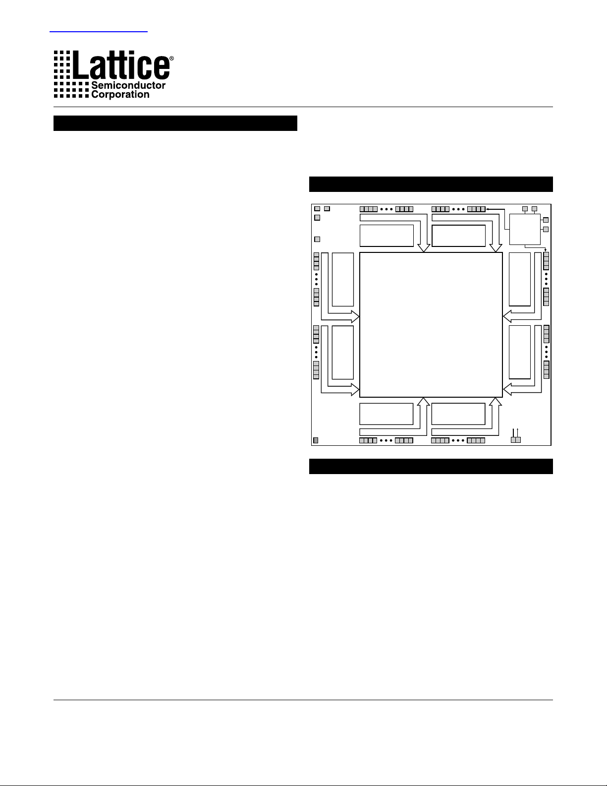
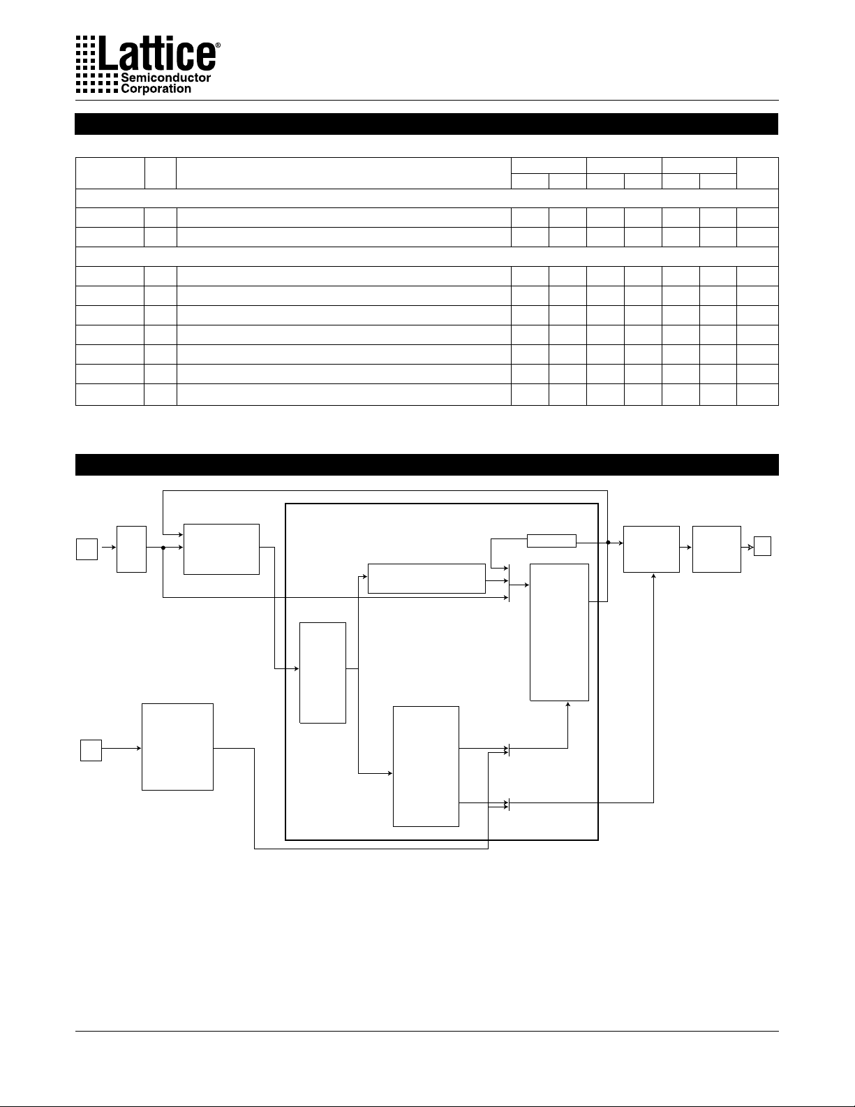
Functional Block Diagram
Generic
Input Bus
Generic
Input Bus
Logic Block
Logic Block
Logic Block
Logic Block
Input Bus
Generic
Global Routing Pool
(GRP)
Generic
Input Bus
Input Bus
Generic
Logic Block
Generic
Logic Block
Input Bus
Boundary
Scan
Interface
Logic Block
Generic
Input Bus
Logic Block
Generic
Input Bus
ispLSI 5000V Description
The ispLSI 5000V Family of In-System Programmable
High Density Logic Devices is based on Generic Logic
Blocks (GLBs) of 32 registered macrocells and a single
Global Routing Pool (GRP) structure interconnecting the
GLBs.
Outputs from the GLBs drive the Global Routing Pool
(GRP) between the GLBs. Switching resources are provided to allow signals in the Global Routing Pool to drive
any or all the GLBs in the device. This mechanism allows
fast, efficient connections across the entire device.
Each GLB contains 32 macrocells and a fully populated,
programmable AND-array with 160 logic product terms
and five extra control product terms. The GLB has 68
inputs from the Global Routing Pool which are available
Copyright © 2000 Lattice Semiconductor Corp. All brand or product names are trademarks or registered trademarks of their respective holders. The specifications and information herein are subject
to change without notice.
LATTICE SEMICONDUCTOR CORP., 5555 Northeast Moore Ct., Hillsboro, Oregon 97124, U.S.A. September 2000
Tel. (503) 268-8000; 1-800-LATTICE; FAX (503) 268-8556; http://www.latticesemi.com
15256va_04

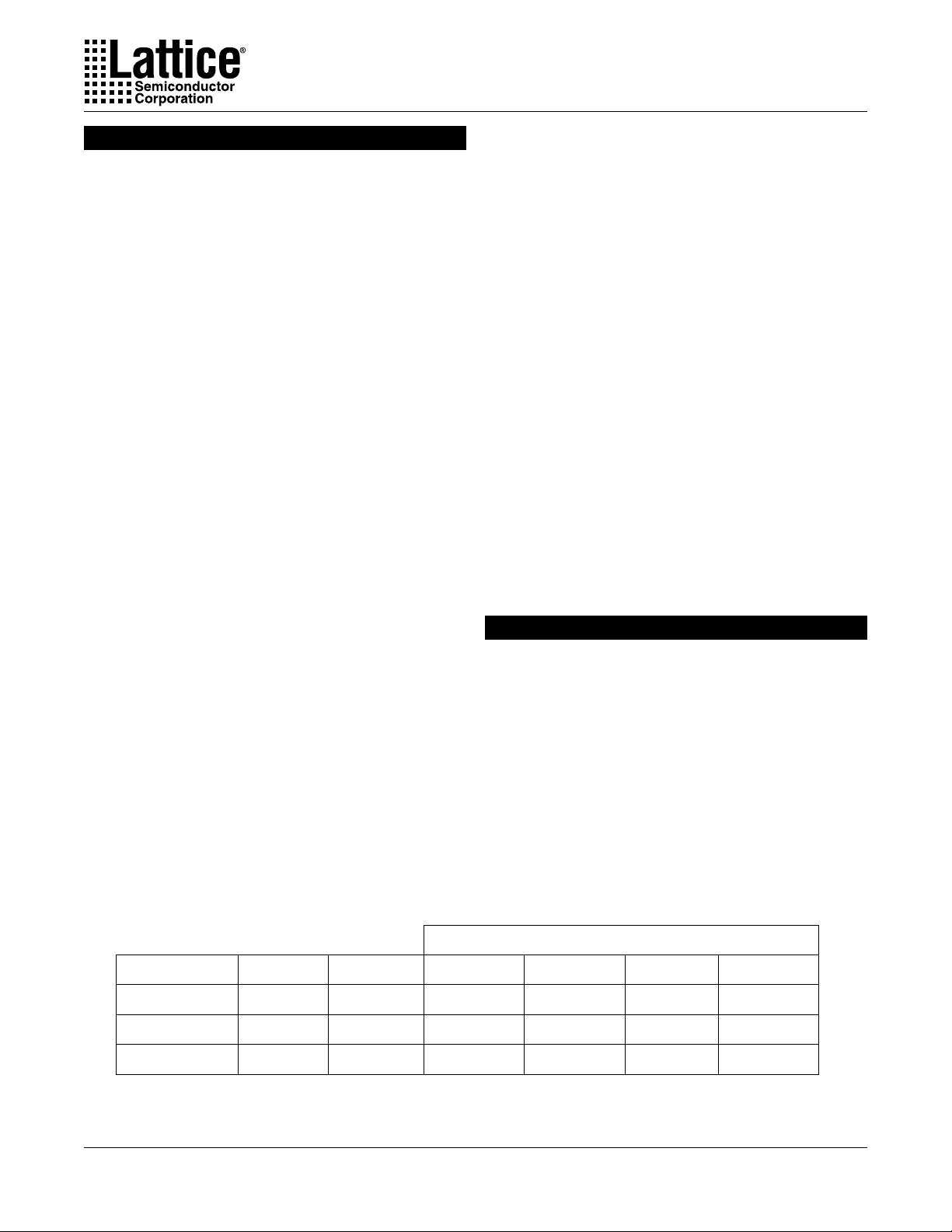
Specifications ispLSI 5256VA
Functional Block Diagram
Figure 1. ispLSI 5256VA Functional Block Diagram (272 BGA Option)
GOE0
GOE1
I/O 191
I/O 190
I/O 189
I/O 188
I/O 171
I/O 170
I/O 169
I/O 168
I/O 167
I/O 166
I/O 165
I/O 164
I/O 147
I/O 146
I/O 145
I/O 144
TCK
TMS
VCCIO
1
I/O 0 / TOE
I/O 1
I/O 2
I/O 3
I/O 20
I/O 21
I/O 22
I/O 23
I/O 24
I/O 25
I/O 26
I/O 27
I/O 44
I/O 45
I/O 46
I/O 47
Generic
Input Bus
Generic
Input Bus
Logic Block
Logic Block
Logic Block
Input Bus
Generic
Input Bus
Generic
Logic Block
Global Routing Pool
(GRP)
Boundary
Scan
Interface
Logic Block
Generic
Input Bus
Logic Block
Generic
Input Bus
TDI
TDO
I/O 143
I/O 142
I/O 141
I/O 140
I/O 123
I/O 122
I/O 121
I/O 120
I/O 119
I/O 118
I/O 117
I/O 116
I/O 99
I/O 98
I/O 97
I/O 96
GSET/GRST
Generic
Logic Block
Input Bus
I/O 48
I/O 49
I/O 50
I/O 51
I/O 68
I/O 69
I/O 70
I/O 71
Generic
Logic Block
Input Bus
I/O 72
I/O 73
I/O 74
I/O 75
I/O 92
I/O 93
I/O 94
I/O 95
CLK 1
CLK 0
CLK 3
CLK 2
1
1
1. CLK2, CLK3 and TOE signals are multiplexed with I/O signals. Which I/O is multiplexed is
determined by the package type used (see table below).
Package Type Multplexed Signals
208 PQFP I/O 89 / CLK2 I/O 98 / CLK3 I/O 0 / TOE
208 fpBGA I/O 89 / CLK2 I/O 98 / CLK3 I/O 0 / TOE
272 BGA I/O 119 / CLK2 I/O 131 / CLK3 I/O 0 / TOE
2
Specifications ispLSI 5256VA
ispLSI 5000V Description (Continued)
in both true and complement form for every product term.
The 160 product terms are grouped in 32 sets of five and
sent into a Product Term Sharing Array (PTSA) which
allows sharing up to a maximum of 35 product terms for
a single function. Alternatively, the PTSA can be bypassed for functions of five product terms or less. The
five extra product terms are used for shared GLB controls, set, reset, clock, clock enable and output enable.
The 32 registered macrocells in the GLB are driven by the
32 outputs from the PTSA or the PTSA bypass. Each
macrocell contains a programmable XOR gate, a programmable register/latch/toggle flip-flop and the
necessary clocks and control logic to allow combinatorial
or registered operation. The macrocells each have two
outputs, which can be fed back through the Global
Routing Pool. This dual output capability from the
macrocell allows efficient use of the hardware resources.
One output can be a registered function for example,
while the other output can be an unrelated combinatorial
function. A direct register input from the I/O pad facilitates efficient use of this feature to construct high-speed
input registers.
Macrocell registers can be clocked from one of several
global or product term clocks available on the device. A
global and product term clock enable is also provided,
eliminating the need to gate the clock to the macrocell
registers. Reset and preset for the macrocell register is
provided from both global and product term signals. The
macrocell register can be programmed to operate as a Dtype register, a D-type latch or a T-type flip flop.
The 32 outputs from the GLB can drive both the Global
Routing Pool and the device I/O cells. The Global
Routing Pool contains one line from each macrocell
output and one line from each I/O pin.
The input buffer threshold has programmable TTL/3.3V/
2.5V compatible levels. The output driver can source
4mA and sink 8mA in 3.3V mode. The output drivers
have a separate VCCIO reference input which is independent of the main VCC supply for the device. This
feature allows the output drivers to drive either 3.3V or
2.5V output levels while the device logic and the output
current drive is always powered from 3.3V. The output
drivers also provide individually programmable edge
rates and open drain capability. A programmable pullup
resistor is provided to tie off unused inputs and a programmable bus-hold latch is available to hold tristate
outputs in their last valid state until the bus is driven again
by some device.
The ispLSI 5000V Family features 3.3V, non-volatile insystem programmability for both the logic and the
interconnect structures, providing the means to develop
truly reconfigurable systems. Programming is achieved
through the industry standard IEEE 1149.1-compliant
Boundary Scan interface. Boundary Scan test is also
supported through the same interface.
An enhanced, multiple cell security scheme is provided
that prevents reading of the JEDEC programming file
when secured. After the device has been secured using
this mechanism, the only way to clear the security is to
execute a bulk-erase instruction.
ispLSI 5000V Family Members
The ispLSI 5000V Family ranges from 256 macrocells to
512 macrocells and operates from a 3.3V power supply.
All family members will be available with multiple package options. The ispLSI 5000V Family device matrix
showing the various bondout options is shown in the table
below.
The interconnect structure (GRP) is very similar to Lattice's
existing ispLSI 1000, 2000 and 3000 families, but with an
enhanced interconnect structure for optimal pin locking
and logic routing. This eliminates the need for registered
I/O cells or an Output Routing Pool.
Table 1. ispLSI 5000V Family
eciveDsBLGsllecorcaMAGBpf802PFQP802AGB272AGB883
AV6525ISLpsi 8652O/I441O/I441O/I291—
AV4835ISLpsi 21483O/I441O/I441O/I291O/I882
AV2155ISLpsi 61215— O/I441O/I291O/I882
epyTegakcaP
3
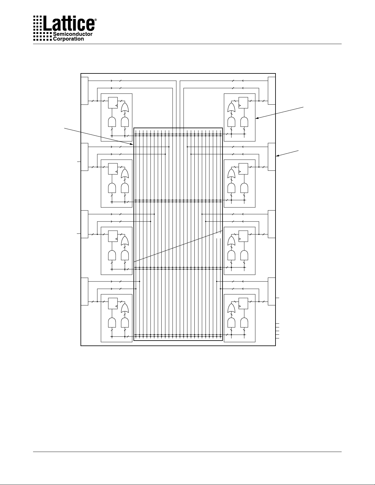
Figure 2. ispLSI 5256VA Block Diagram (192 I/O Version)
24 24
Global
Routing
Pool
(GRP)
24
I/O
24
32
32
DQ
32
160
160
5
PT
PT
5
160
68
Specifications ispLSI 5256VA
32
32
DQ
32
160
160
5
PT
PT
160
68
5
24
I/O
24
Generic
Logic
Block
(GLB)
CLK2
CLK3
24
24
I/O
24
24
I/O
24
24
I/O
24 24
32 32
32
DQ
32
160
160
5
PT
PT
5
160
68
24 24
32 32
32
DQ
32
160
5
160
PT
PT
5
160
68
24 24
32
32
DQ
32
160
160
5
PT
PT
5
160
68
24
32
DQ
160
160
PT
160
68
32
448
DQ
160
160
PT
160
68
32
32
DQ
160
160
PT
160
68
24
I/O
32
24
5
PT
5
24
I/O
32
24
5
PT
5
24
I/O
5512_384
TOE
CLK0
CLK1
GOE0
GOE1
SET/RESET
32
5
PT
5
Buffers/Pins
4
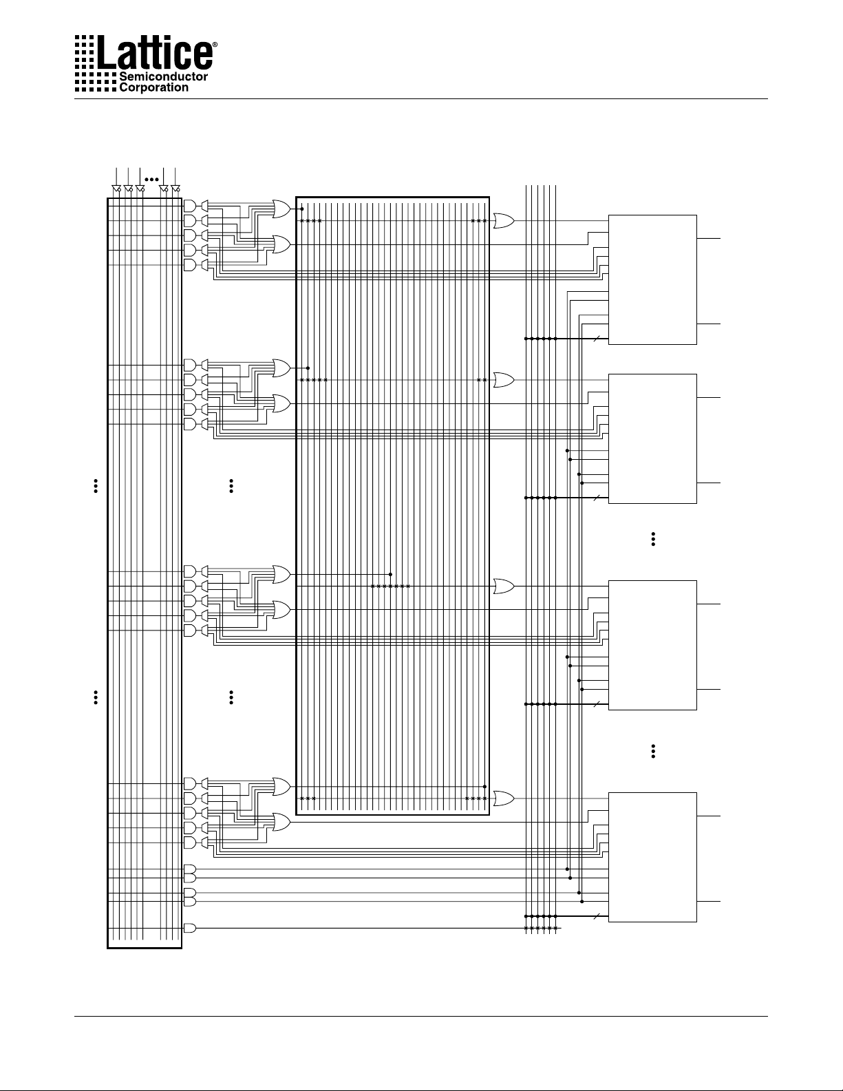
Figure 3. ispLSI 5000V Generic Logic Block (GLB)
From Global Routing Pool
0126667
PTSA
PT 0
PT 1
PT 2
PT 3
PT 4
PT 9
PT 8
PT 7
PT 6
PT 5
Specifications ispLSI 5256VA
Global PTOE Bus
Macrocell 0
From PTSA
PTSA bypass
PTOE
PT Clock
PT Reset
PT Preset
Shared PT Clock 0
Shared PT (P)reset 0
Shared PT Clock 1
Shared PT (P)reset 1
Global PTOE 0 ... 5
6
Macrocell 1
From PTSA
PTSA bypass
PTOE
PT Clock
PT Reset
PT Preset
Shared PT Clock 0
Shared PT (P)reset 0
Shared PT Clock 1
Shared PT (P)reset 1
Global PTOE 0 ... 5
6
To I/O Pad
To GRP
To I/O Pad
To GRP
PT 79
PT 78
PT 77
PT 76
PT 75
PT 159
PT 158
PT 157
PT 156
PT 155
PT 160
PT 161
PT 162
PT 163
PT 164
Programmable
AND Array
Macrocell 15
From PTSA
PTSA bypass
PTOE
PT Clock
PT Reset
PT Preset
Shared PT Clock 0
Shared PT (P)reset 0
Shared PT Clock 1
Shared PT (P)reset 1
Global PTOE 0 ... 5
6
Macrocell 31
From PTSA
PTSA bypass
PTOE
PT Clock
PT Reset
PT Preset
Shared PT Clock 0
Shared PT (P)reset 0
Shared PT Clock 1
Shared PT (P)reset 1
Global PTOE 0 ... 5
6
To I/O Pad
To GRP
To I/O Pad
To GRP
GLB_5K
5
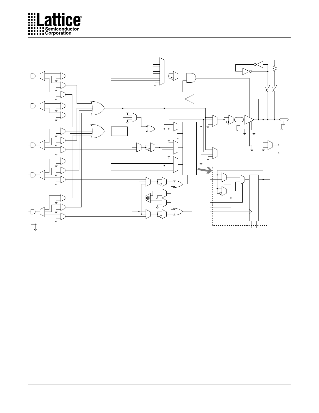
Figure 4. ispLSI 5000V Macrocell
Specifications ispLSI 5256VA
PTOE
PT Clock
PT Reset
PT Preset
GOE0
GOE1
TOE
Shared PT Clock 0
Shared PT Clock 1
CLK0
CLK1
CLK2
CLK3
SET/RESET
Shared PT (P)reset 0
Shared PT (P)reset 1
PTSA
Global PTOE 0
Global PTOE 1
Global PTOE 2
Global PTOE 3
Global PTOE 4
Global PTOE 5
PTSA bypass
DQ
D/T
Clk En
R/L
Clk
RP
D/T
Clk En
Clk
Delay
Slew
rate
2.5V/3.3V
Output
Open
drain
DQD
VCCIOVCCIO VCC
To GRP
Q
Register/
Latch
I/O Pad
Programmable
Speed/Power
Option
RP
6
Specifications ispLSI 5256VA
Global Clock Distribution
The ispLSI 5000V Family has four dedicated clock input
pins: CLK0 - CLK3. CLK0 input is used as the dedicated
master clock that has the lowest internal clock skew with
no clock inversion to maintain the fastest internal clock
Figure 5. ispLSI 5000V Global Clock Structure
CLK 0
CLK 1
IO/CLK 2
IO/CLK 3
speed. The clock inversion is available on the remaining
CLK1 - CLK3 signals. By sharing the pins with the I/O
pins, CLK2 and CLK3 can not only be inverted but also is
available for logic implementation through GRP signal
routing. Figure 5 shows these different clock distribution
options.
CLK0
CLK1
To GRP
CLK2
CLK3
To GRP
GSET/GRST
SET/RESET
7
Figure 6. Boundary Scan Register Circuit for I/O Pins
Specifications ispLSI 5256VA
HIGHZ
EXTEST
SCANIN
(from previous
cell)
Shift DR
Clock DR
BSCAN
Registers
DQ DQ
DQ
DQ
Update DR
BSCAN
Latches
DQ
Reset
TOE
Normal
Function
EXTEST
PROG_MODE
Normal
Function
OE
SCANOUT
(to next cell)
0
1
0
1
I/O Pin
Figure 7. Boundary Scan Register Circuit for Input-Only Pins
Input Pin
SCANIN
DQ
(from previous
cell)
Shift DR
Clock DR
8
SCANOUT
(to next cell)

Specifications ispLSI 5256VA
Figure 8. Boundary Scan Waveforms and Timing Specifications
TMS
TDI
TCK
TDO
Data to be
captured
Data to be
driven out
T
btch
T
T
btvo
T
T
btcl
T
btuov
btsu
btcpsu
Data Captured
T
bth
T
btcp
T
btco
Valid Data Valid Data
T
btcph
T
btuco
Valid Data Valid Data
T
btoz
T
btuoz
SYMBOL PARAMETER MIN MAX UNITS
t
btcp TCK [BSCAN test] clock pulse width
t
btch TCK [BSCAN test] pulse width high
t
btcl TCK [BSCAN test] pulse width low
t
btsu TCK [BSCAN test] setup time
t
bth TCK [BSCAN test] hold time
t
rf TCK [BSCAN test] rise and fall time
t
btco TAP controller falling edge of clock to valid output
t
btoz TAP controller falling edge of clock to data output disable
t
btvo TAP controller falling edge of clock to data output enable
t
btcpsu BSCAN test Capture register setup time
t
btcph BSCAN test Capture register hold time
t
btuco BSCAN test Update reg, falling edge of clock to valid output
t
btuoz BSCAN test Update reg, falling edge of clock to output disable
t
btuov BSCAN test Update reg, falling edge of clock to output enable
125 – ns
62.5 – ns
62.5 – ns
25 – ns
25 – ns
50 – mV/ns
– 25 ns
– 25 ns
– 25 ns
25 – ns
25 – ns
– 50 ns
– 50 ns
– 50 ns
9

Specifications ispLSI 5256VA
Absolute Maximum Ratings
1, 2
Supply Voltage Vcc.................................. -0.5 to +5.4V
Input Voltage Applied............................... -0.5 to +5.6V
Tri-Stated Output Voltage Applied........... -0.5 to +5.6V
Storage Temperature................................ -65 to 150°C
Case Temp. with Power Applied .............. -55 to 125°C
Max. Junction Temp. (TJ) with Power Applied ... 150°C
1. Stresses above those listed under the “Absolute Maximum Ratings” may cause permanent damage to the device. Functional
operation of the device at these or at any other conditions above those indicated in the operational sections of this specification
is not implied (while programming, follow the programming specifications).
2. Compliance with the Thermal Management section of the Lattice Semiconductor Data Book or CD-ROM is a requirement.
DC Recommended Operating Condition
MIN. MAX. UNITS
3.00
3.00 3.60 V
2.3
3.60
3.60
Table 2 - 0005/5256
V
V
V
V
CC
CCIO
SYMBOL
PARAMETER
Supply Voltage
I/O Reference Voltage
Commercial
Industrial
= 0°C to +70°C
T
A
T
= -40°C to +85°C
A
Capacitance (TA=25°C,f=1.0 MHz)
SYMBOL
C
1
C
2
C
3
PARAMETER
I/O Capacitance
Clock Capacitance
Global Input Capacitance
10
10
10
UNITSTYPICAL TEST CONDITIONS
pf V = 3.3V, V = 2.0V
pf V = 3.3V, V = 2.0V
pf V = 3.3V, V = 2.0V
CC I/O
CC CK
CC G
Table 2 - 0006/5384
Erase Reprogram Specification
PARAMETER MINIMUM MAXIMUM UNITS
ispLSI Erase/Reprogram Cycles 10000 – Cycles
Table 2-0008/3320
10
Switching Test Conditions
Input Pulse Levels
Input Rise and Fall Time
Input Timing Reference Levels
Ouput Timing Reference Levels
Output Load
3-state levels are measured 0.5V from steady-state
active level.
GND to V
≤ 1.5ns 10% to 90%
Output Load Conditions (See Figure 8)
3.3V 2.5V
TEST CONDITION R1
A 35pF
Active High
B
Active Low
Active High to Z
at V -0.5V
C
D 35pF
OH
Active Low to Z
at V +0.5V
OL
Slow Slew
R1 R2
316Ω
∞
316Ω
∞
316Ω
∞
348Ω
348Ω
∞
348Ω
∞
∞
511Ω
∞
511Ω
∞
511Ω
∞
CCIO
1.5V
1.5V
See figure
Table 2 - 0003/5384
R2 CL
475Ω
475Ω
∞
475Ω
∞
∞
Table 2 - 0004A/5384
min
35pF
35pF
5pF
5pF
Specifications ispLSI 5256VA
Figure 9. Test Load
V
CCIO
R
1
Device
Output
R
2
*
CL includes Test Fixture and Probe Capacitance.
C
*
L
Test
Point
0213D
DC Electrical Characteristics for 3.3V Range
Over Recommended Operating Conditions
SYMBOL
VCCIO
VIL
VIH
VOL
VOH
I/O Reference Voltage 3.0 – 3.6 V
Input Low Voltage
Input High Voltage
Output Low Voltage
Output High Voltage
1. I/O voltage configuration must be set to VCC.
PARAMETER
V
OH
V
OH
= 8 mA
I
OL
I
OH
1
CONDITION MIN. TYP. MAX. UNITS
≤ V
OUT
≤ V
OUT
= -4 mA
or V
or V
≤ V
OUT
≤ VOL(max)
OUT
OL (max)
-0.3
2.0
–
2.4
–
–
–
–
0.8
5.25
0.4
–
Table 2-0007/5256VA
V
V
V
V
11

Specifications ispLSI 5256VA
DC Electrical Characteristics for 2.5V Range
Over Recommended Operating Conditions
SYMBOL
V
V
V
V
V
CCIO
IL
IH
OL
OH
I/O Reference Voltage
Input Low Voltage
Input High Voltage
Output Low Voltage
Output High Voltage
1. I/O voltage configuration must be set to VCCIO.
PARAMETER
V
OH(min)
V
OH(min)
V
CCIO=min
V
CCIO=min
V
CCIO=min
V
CCIO=min
DC Electrical Characteristics
Over Recommended Operating Conditions
SYMBOL
IIL
IIH
1
IPU
IBHL
IBHH
IBHLO
IBHLH
IBHT
IVCCIO
Input or I/O Low Leakage Current 0V ≤ V ≤ V (Max.)
Input or I/O High Leakage Current
I/O Active Pullup Current
Bus Hold Low Sustaining Current
Bus Hold High Sustaining Current
Bus Hold Low Overdrive Current
Bus Hold High Overdrive Current
Bus Hold Trip Points
Current Needed for V
1. Pullup is capable of pulling to a minimum voltage of V
PARAMETER
Pin All I/Os Pulled-up, (Total I/Os * I
CCIO
(V
CCIO
V
≤ VIN ≤ 5.25V
CCIO
0V
≤ VIN ≤ V
VIN = V
VIN = V
0V ≤ VIN ≤ V
0V ≤ VIN ≤ V
under no-load conditions.
OH
1
CONDITION MIN. TYP. MAX. UNITS
≤ V
≤ V
or V
OUT
or V
OUT
, VIN=VIH or VIL, IOL= 100µA
, VIN=VIH or VIL, IOL= 2mA
, VIN=VIH or VIL, IOH= -100µA
, VIN=VIH or VIL, IOH= -2mA
OUT
OUT
≤ V
≤ V
OL(max)
OL(max)
2.3
-0.3
1.7
––0.2 V
––0.7 V
2.1 ––V
1.7
–
–
–
5.25
–
CONDITION MIN. TYP. MAX. UNITS
IN IL
-0.2)V ≤ VIN ≤ V
IL
IL(max)
IH(min)
CCIO
CCIO
CCIO
–
–
–
–
40
-40
–
–
V
IL
) ––30 mA
PUmax
–
–
–
–
-150
–
–
–
550
–
-550
–
2.7
0.7
–
2.5V/5256VA
-10
10
50
–
–
V
IH
DC Char_5256VA
V
V
V
V
µA
µA
µA
µA
µA
µA
µA
µA
V
12

External Switching Characteristics
Over Recommended Operating Conditions
3
.MARAP
6
t
1dp
6
t
2dp
f
xam
f
f
t
t
t
1h
t
t
2h
t
t
t
t
t
1r
t
t
t
t
t
hw
t
lw
).txE(xam
).goT(xam
1us
6
1oc
2us
)1/0KLC(3us
)3/2KLC(3us
)1/0KLC(3h
)3/2KLC(3h
1wr
sid/eotp
sid/eotpg
sid/eog
TSET
#NOITPIRCSED
.DNOC
A1 ssapyBTP5,yaleD.porPataD — 5.7 — 01 — 51sn
A2 yaleDnoitagaporPataD — 5.9 — 31 — 91sn
A3 kcabdeeFlanretnIhtiwycneuqerFkcolC
— 4)1oct+2ust(/1,kcabdeeF.txEhtiw.qerFkcolC19 — 96 — 54 — zHM
— 5elggoTxaM,ycneuqerFkcolC
— 6ssapybTP5,klCerofebemiTputeS.geRBLG6— 8 — 21 — sn
A7 yaleDtuptuOotkcolC.geRBLG — 4 — 5.5 — 8sn
— 8ssapybTP5,kcolCretfaemiTdloH.geRBLG0— 0 — 0 — sn
— 9kcolCerofebemiTputeS.geRBLG7— 9 — 41 — sn
— 01kcolCretfaemiTdloH.geRBLG0— 0 — 0 — sn
— 11
— 21
— 31
— 41
A51yaleDtuptuOotniPteseR.txE — 51 — 02 — 03sn
— 61noitaruDesluPteseR.txE7— 9 — 41 — sn
C/B71elbasiD/elbanEtuptuOmreTtcudorPlacoL — 9 — 21 — 81sn
C/B81elbasiD/elbanEtuptuOmreTtcudorPlabolG — 81 — 42 — 03sn
C/B91elbasiD/elbanEtuptuOottupnIEOlabolG — 6 — 8 — 21sn
— 02hgiH,noitaruDesluPkcolC.cnyS.txE3— 4 — 6 — sn
— 12woL,noitaruDesluPkcolC.cnyS.txE3— 4 — 6 — sn
.ecnereferegatlovO/Isadesu
spe.0.4/av6525.txEgnimiT
)1/0KLC(htaP
)3/2KLC(htaP
)1/0KLC(
)3/2KLC(
.kcabdeefPRGgnisuretnuoctib-23dradnatS.1
.noitcessnoitidnoCtseTgnihctiwSecnerefeR.3
Specifications ispLSI 5256VA
5,4
1
2
.geRtupnI,kcolCerofebemiTputeS.geRBLG
.geRtupnI,kcolCerofebemiTputeS.geRBLG
htaP.geRtupnI,kcolCretfaemiTdloH.geRBLG
htaP.geRtupnI,kcolCretfaemiTdloH.geRBLG
.revirdtuptuoevitcalamrongnisuderusaemsretemarapgnimiT.5
521-001-07-
.NIM.XAM.NIM.XAM.NIM.XAM
521 — 001 — 07 — zHM
761 — 521 — 38 — zHM
5.4 — 6 — 9 — sn
5.3 — 5 — 7 — sn
0 — 0 — 0 — sn
0 — 0 — 0 — sn
.%05nahtrehtofoelcycytudkcolcarofwollaotsisihT.)lwt+hwt(/1nahtsselebyam)elggoT(xamf.2
.0KLCdna,BLG1fodaolPRGa,tuonafASTPesactsrowhtiwnekaterasrebmungnimitlla,esiwrehtodetonsselnU.4
STINU
sioiccVnehwderrucnisiyaledsn5.0lanoitiddanA.ecnereferegatlovO/IsaccVhtiwderusaemerasretemarapyaledehT.6
13

Specifications ispLSI 5256VA
Internal Timing Parameters
1
Over Recommended Operating Conditions
PARAM #
I/O Buffer
2
DESCRIPTION
tidcom 22 Input Pad and Buffer, Combinatorial Input – 0.7 – 0.9 – 1.4 ns
tidreg 23 Input Pad and Buffer, Registered Input – 4.7 – 6.6 – 9.7 ns
todcom 24 Output Pad and Buffer, Combinatorial Output – 1.3 – 1.7 – 2.6 ns
todreg 25 Output Pad and Buffer, Registered Output – 1.8 – 2.8 – 4.6 ns
todz 26 Output Buffer Enable/Disable – 1.3 – 1.7 – 2.6 ns
tslf 27 Slew Rate Adder, Fast Slew – 0 – 0 – 0ns
tsls 28 Slew Rate Adder, Slow Slew – 7.5 – 10 – 15 ns
tslfd 29 Programmable Delay Adder, Fast Slew – 0.5 – 0.7 – 1ns
tslsd 30 Programmable Delay Adder, Slow Slew – 8 – 10.7 – 16 ns
GLB/Macrocell Delay Register
tmbp 31 Macrocell Register/Latch Bypass – 0 – 0 – 0ns
tmlat 32 Macrocell Latch Delay – 1 – 1.4 – 2ns
tmco 33 Macrocell Register/Latch Clock to Output – 1 – 1 – 1ns
tmsu 34 Macrocell Register/Latch Setup Time 1 – 1.1 – 1.7 – ns
tmh 35 Macrocell Register/Latch Hold Time 2.5 – 3.9 – 5.3 – ns
tmsuce 36 Macrocell Register/Latch CLKEN Setup Time 1 – 1.4 – 2 – ns
tmhce 37 Macrocell Register/Latch CLKEN Hold Time 1 – 1.4 – 2 – ns
tmrst 38 Macrocell Register/Latch Set/Reset Time – 1 – 1.4 – 2ns
tftog 39 Toggle Flip-Flop Feedback – 1 – 1.3 – 2ns
AND Array
tandhs 40 AND Array, High Speed Mode – 3 – 4 – 6ns
tandlp 41 AND Array, Low Power Mode – 5 – 6.6 – 10 ns
PTSA
t5ptcom 42 5 Product Term Bypass, Combinatorial – 1 – 1.4 – 2ns
t5ptreg 43 5 Product Term Bypass, Registered – 1 – 1.7 – 2.3 ns
t5ptxcom 44 5 Product Term XOR, Combinatorial – 2.5 – 3.6 – 5ns
t5pxtreg 45 5 Product Term XOR, Registered – 1.5 – 2.2 – 3.3 ns
tptsacom 46 Product Term Sharing Array, Combinatorial – 3 – 4.1 – 6ns
tptsareg 47 Product Term Sharing Array, Registered – 2.0 – 2.7 – 4.3 ns
PTSA Controls
tpck 48 Product Term Clock Delay – 0.5 – 0.7 – 1ns
tpcken 49 Product Term CLKEN Delay – 1 – 1.4 – 2ns
tscken 50 Shared Product Term CLKEN Delay – 1 – 1.4 – 2ns
tsck 51 Shared Product Term Clock Delay – 0.5 – 0.7 – 1ns
tptsacken 52 Product Term Sharing Array CLKEN Delay – 2.0 – 2.4 – 4ns
tsrst 53 Shared Product Term Set/Reset Delay – 2.5 – 3.4 – 5ns
tprst 54 Product Term Set/Reset Delay – 1.5 – 2 – 3ns
tpoe 55 Product Term Output Enable/Disable – 2.5 – 3.4 – 5ns
tgpoe 56 Global PT Output Enable/Disable – 11.5 – 15.4 – 17 ns
-125 -100 -70
MIN MAX MIN MAX MIN MAX UNIT
1. Internal Timing Parameters are not tested and are for reference only. Timing Rev. 4.0
2. Refer to Timing Model in this data sheet for further details.
14
Specifications ispLSI 5256VA
Internal Timing Parameters
1
Over Recommended Operating Conditions
PARAM #
2
DESCRIPTION
GRP
tgrpi 57 GRP Delay from I/O Pad – 1.5 – 2 – 3ns
tgrpm 58 GRP Delay from Macrocell – 1.0 – 1.2 – 1.2 ns
Global Control Delays
tgclk01 59 Global Clock 0 or 1 Delay – 1.2 – 1.7 – 2.4 ns
tgclk23 60 Global Clock 2 or 3 Delay – 2.2 – 2.7 – 4.4 ns
tgclken0 61 Global CLKEN 0 Delay – 1.7 – 2.4 – 3.4 ns
tgclken1 62 Global CLKEN 1 Delay – 2.7 – 3.4 – 5.4 ns
tgrst 63 Global Set/Reset Delay – 12.2 – 15.8 – 23.4 ns
tgoe 64 Global OE Delay – 4.7 – 6.3 – 9.4 ns
ttoe 65 Test OE Delay – 4.7 – 6.2 – 9.4 ns
1. Internal Timing Parameters are not tested and are for reference only. Timing Rev. 4.0
2. Refer to Timing Model in this data sheet for further details.
-125 -100 -70
MIN MAX MIN MAX MIN MAX UNIT
ispLSI 5256VA Timing Model
Output
Buffer
Buffer Delays
t
#22
odcom
t
#23
odreg
t
#24
odz
#28
#27
#25
#26
Slew
t
t
t
t
slsd
slfd
slf
sls
I/O
Pad
OUTPUT
I/O
Pad
INPUT
Input
Pad
Input
Buffer
#20
t
idcom
t
idreg
#21
#56
#55
Dedicated
Input Buffers
t
#57
gclk0
t
#58
gclk123
t
#59
gclken0
t
#60
gclken1
#61
t
grst
t
#62
goe
t
#63
toe
GRP
t
grpm
t
grpi
AND Array
#38
t
andhs
t
andlp
#39
GLB/Macrocell
PTSA
t
#40
5ptcom
t
#44
ptsacom
t
#42
5ptxcom
PT Controls
#49
#46
#50
#47
#48
#51
#52
#53
#54
#41
#45
#43
t
sck
t
pck
t
ptsacken
tpcken
tscken
t
srst
t
prst
t
poe
t
gpoe
t
5ptxreg
t
ptsareg
t
5ptreg
t
#37
ftog
Register
t
#29
mbp
t
mlat
#30
t
#32
msu
t
#33
mh
t
#31
mco
#35
t
mhce
t
msuce
#34
#36
t
mrst
15
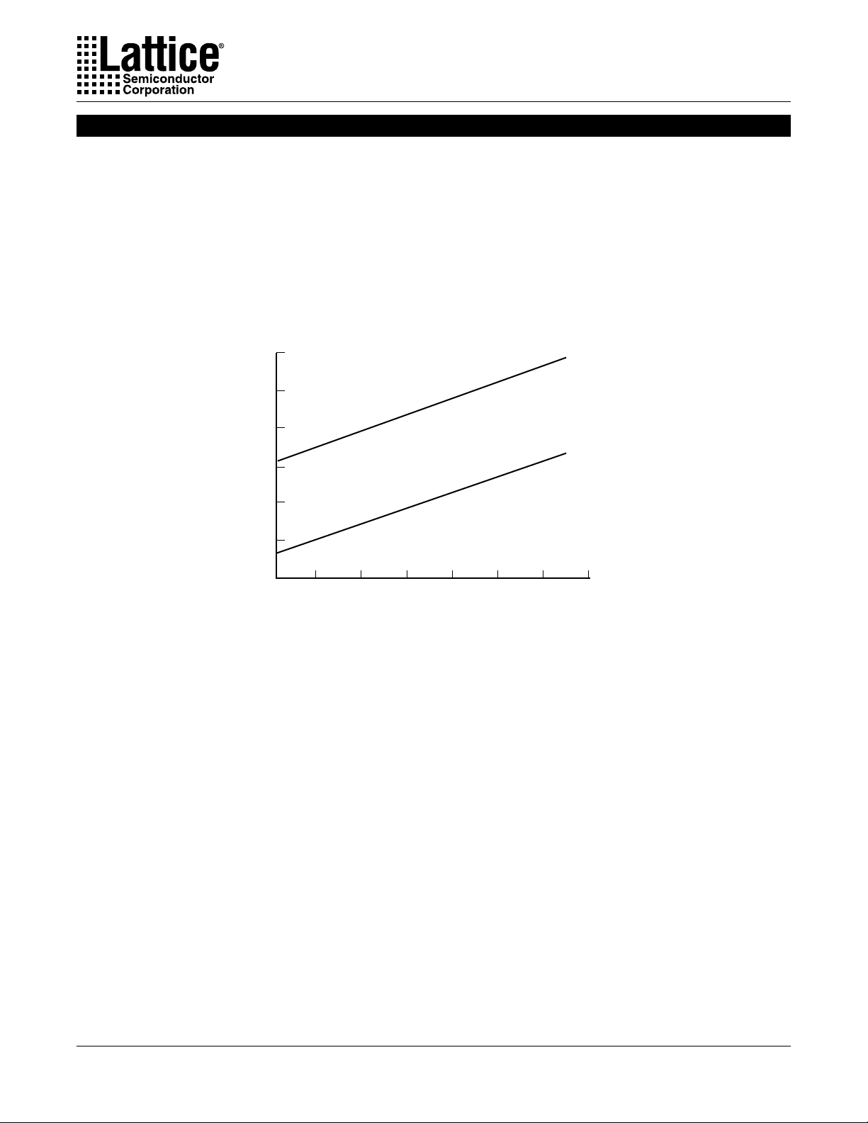
Power Consumption
Specifications ispLSI 5256VA
Power consumption in the ispLSI 5256VA device depends on two primary factors: the speed at which the
device is operating and the number of product terms
used. The product terms have a fuse-selectable speed/
power tradeoff setting. Each group of four product terms
has a single speed/power tradeoff control fuse that acts
Figure 10. Typical Device Power Consumption vs fmax
400
ispLSI 5256VA
High Speed Mode
350
300
250
(mA)
CC
I
200
150
on the complete group of four. The fast “high-speed”
setting operates product terms at their normal full power
consumption. For portions of the logic that can tolerate
longer propagation delays, selecting the slower “lowpower” setting will significantly reduce the power
dissipation for these product terms. Figure 10 shows the
relationship between power and operating speed.
ispLSI 5256VA
Low Power Mode
100
0 20 40 60 80 100 120 140
f
max (MHz)
Notes: Configuration of 16 16-bit Counters
Typical Current at 3.3V, 25° C
ICC can be estimated for the ispLSI 5256VA using the following equation:
High Speed Mode: ICC = 30 + (# of PTs * 0.456) + (# of nets * Max. freq * 0.0039)
Low Power Mode: ICC = 30 + (# of PTs * 0.22) + (# of nets * Max. freq * 0.0039)
# of PTs = Number of Product Terms used in design
# of nets = Number of Signals used in device
Max. freq = Highest Clock Frequency to the device
The I
on average exists. These values are for estimates only. Since the value of I
and the program in the device, the actual I
estimate is based on typical conditions (VCC = 3.3V, room temperature) and an assumption of 2 GLB loads
CC
should be verified.
CC
is sensitive to operating conditions
CC
0127/5256va
16

Specifications ispLSI 5256VA
Signal Descriptions
Signal Name Description
TMS Input - This pin is the Test Mode Select input, which is used to control the JTAG state machine.
TCK Input - This pin is the Test Clock input pin used to clock through the JTAG state machine.
TDI Input - This pin is the JTAG Test Data In pin used to load data.
TDO Output - This pin is the JTAG Test Data Out pin used to shift data out.
TOE / I/O0 Input/Output - This pin functions as either the Test Output Enable pin or an I/O pin based upon
customer's design. TOE tristates all I/O pins when a logic low is driven.
GOE0, GOE1 Input - These two pins are the Global Output Enable input pins.
GSET/GRST Dedicated Set/Reset Input - This pin is available to all registers in the device and can
independently be configured as preset, reset or no effect on each register. The global polarity
(active high or low input) for this pin is also selectable.
I/O Input/Output – These are the general purpose I/O used by the logic array.
GND Ground
1
NC
VCC Vcc
CLK0, CLK1 Dedicated clock inputs for all registers. Both clocks are muxed before being used as the clock
CLK2 / I/O, Input/Output - These pins function as either dedicated clock inputs for all registers or an I/O
CLK3 / I/O pin based upon customer's design. Both clocks are muxed before being used as the clock input
VCCIO Input - This pin is used if an optional 2.5V output is to be used. Every I/O can independently
1. NC pins are not to be connected to any active signals, VCC or GND.
No connect.
input to all registers in the device.
to all registers in the device.
select either 3.3V or the optional voltage as its output level. If the optional output voltage is
not required, this pin must be connected to the Vcc supply. Programmable pull-up resistors and
bus-hold latches only draw current from this supply.
17
Specifications ispLSI 5256VA
208-Pin PQFP Signal Locations
Signal Pin
GOE0, GOE1 78, 79
TOE / I/O0 32
GSET/GRST 138
TCK 29
TDI 30
TDO 136
TMS 28
CLK0, CLK1 184,185
CLK2 / I/O89 162
CLK3 / I/O98 173
VCCIO 137
GND 3, 12, 19, 27, 39, 48, 58, 69, 77, 88, 99, 113, 121, 128, 135, 150, 164, 170, 179, 191, 199
VCC 7, 14, 22, 31, 41, 61, 80, 90, 110, 123, 139, 152, 156, 177, 186, 201
NC 49, 50, 51, 52, 101, 102, 103, 104, 105, 106, 107, 108, 109, 157, 158, 207, 208
1. NCs are not to be connected to any active signals, VCC or GND.
208-Pin PQFP I/O Locations
I/O # Pin I/O # Pin I/O # Pin I/O # Pin I/O # Pin I/O # Pin
0* 32
133
234
335
436
537
638
740
842
943
10 44
11 45
12 46
13 47
14 53
15 54
16 55
17 56
18 57
19 59
20 60
21 62
22 63
23 64
* I/O 89 is multiplexed with CLK2, I/O 98 is multiplexed with CLK3 and I/O 0 is multiplexed with TOE.
24 65
25 66
26 67
27 68
28 70
29 71
30 72
31 73
32 74
33 75
34 76
35 81
36 82
37 83
38 84
39 85
40 86
41 87
42 89
43 91
44 92
45 93
46 94
47 95
48 96
49 97
50 98
51 100
52 111
53 112
54 114
55 115
56 116
57 117
58 118
59 119
60 120
61 122
62 124
63 125
64 126
65 127
66 129
67 130
68 131
69 132
70 133
71 134
72 140
73 141
74 142
75 143
76 144
77 145
78 146
79 147
80 148
81 149
82 151
83 153
84 154
85 155
86 159
87 160
88 161
89* 162
90 163
91 165
92 166
93 167
94 168
95 169
96 171
97 172
98* 173
99 174
100 175
101 176
102 178
103 180
104 181
105 182
106 183
107 187
108 188
109 189
110 190
111 192
112 193
113 194
114 195
115 196
116 197
117 198
118 200
119 202
120 203
121 204
122 205
123 206
124 1
125 2
126 4
127 5
128 6
129 8
130 9
131 10
132 11
133 13
134 15
135 16
136 17
137 18
138 20
139 21
140 23
141 24
142 25
143 26
18

Specifications ispLSI 5256VA
208-Ball fpBGA Signal Locations
Signal Ball
GOE0, GOE1 P9, P10
TOE / I/O0 K1
GSET/GRST H14
TCK K2
TDI K3
TDO G14
TMS J1
CLK0, CLK1 A7, B8
CLK2 / I/O89 B13
CLK3 / I/O98 A11
VCCIO H15
GND D10, D12, D13, D5, D7, D8, E4, F13, G4, G8, G9, H10, H13, H7, J10, J13, J4, J7, K8, K9, L13, L4,
M13, N10, N12, N4, N5, N7, N8
VCC D11, D4, D6, D9, E13, F4, G10, G13, G7, H4, H8, H9, J8, J9, K10, K13, K4, K7, M4, N11, N13, N6, N9
1
NC
1. NCs are not to be connected to any active signals, VCC or GND.
E15, C14
208-Ball fpBGA I/O Locations (Sorted by I/O)
I/O # Ball I/O # Ball I/O # Ball I/O # Ball I/O # Ball I/O # Ball
0* K1
1L2
2L1
3L3
4M1
5M2
6M3
7N1
8N3
9N2
10 P2
11 P1
12 R1
13 R2
14 R3
15 P3
16 T1
17 P4
18 R4
19 R5
20 P5
21 T2
22 R6
23 T3
* I/O 89 is multiplexed with CLK2, I/O 98 is multiplexed with CLK3 and I/O 0 is multiplexed with TOE.
24 T4
25 T5
26 R7
27 P6
28 T6
29 T7
30 R8
31 P8
32 P7
33 T8
34 T9
35 R9
36 R10
37 T10
38 T11
39 T12
40 T13
41 T14
42 P11
43 P12
44 R11
45 T15
46 T16
47 R14
48 R12
49 P14
50 P13
51 R13
52 R15
53 P15
54 R16
55 P16
56 N15
57 N14
58 M14
59 N16
60 M15
61 M16
62 L14
63 L15
64 L16
65 K14
66 K15
67 K16
68 J14
69 J15
70 J16
71 H16
72 G16
73 F14
74 G15
75 F16
76 E14
77 F15
78 E16
79 D16
80 C16
81 B16
82 D15
83 D14
84 A16
85 C15
86 B15
87 A15
88 B14
89* B13
90 C13
91 A14
92 C12
93 B12
94 A13
95 A12
96 C11
97 B11
98* A11
99 B10
100 A10
101 C10
102 B9
103 C9
104 A9
105 A8
106 C8
107 C7
108 B7
109 A6
110 A5
111 C6
112 B6
113 A4
114 A3
115 A2
116 C5
117 B5
118 B4
119 C4
120 C3
121 C2
122 B3
123 B2
124 A1
125 D2
126 B1
127 D3
128 E2
129 C1
130 E3
131 D1
132 F2
133 E1
134 F1
135 G2
136 F3
137 H2
138 H3
139 G3
140 G1
141 H1
142 J2
143 J3
19

Specifications ispLSI 5256VA
208-Ball fpBGA I/O Locations (Sorted by Ball)
I/O # Ball I/O # Ball I/O # Ball I/O # Ball I/O # Ball I/O # Ball
124 A01
115 A02
114 A03
113 A04
110 A05
109 A06
105 A08
104 A09
100 A10
98* A11
95 A12
94 A13
91 A14
87 A15
84 A16
126 B01
123 B02
122 B03
118 B04
117 B05
112 B06
108 B07
102 B09
99 B10
* I/O 89 is multiplexed with CLK2, I/O 98 is multiplexed with CLK3 and I/O 0 is multiplexed with TOE.
97 B11
93 B12
89* B13
88 B14
86 B15
81 B16
129 C01
121 C02
120 C03
119 C04
116 C05
111 C06
107 C07
106 C08
103 C09
101 C10
96 C11
92 C12
90 C13
85 C15
80 C16
131 D01
125 D02
127 D03
83 D14
82 D15
79 D16
133 E01
128 E02
130 E03
76 E14
78 E16
134 F01
132 F02
136 F03
73 F14
77 F15
75 F16
140 G01
135 G02
139 G03
74 G15
72 G16
141 H01
137 H02
138 H03
71 H16
142 J02
143 J03
68 J14
69 J15
70 J16
0* K01
65 K14
66 K15
67 K16
2 L01
1 L02
3 L03
62 L14
63 L15
64 L16
4 M01
5 M02
6 M03
58 M14
60 M15
61 M16
7 N01
9 N02
8 N03
57 N14
56 N15
59 N16
11 P01
10 P02
15 P03
17 P04
20 P05
27 P06
32 P07
31 P08
42 P11
43 P12
50 P13
49 P14
53 P15
55 P16
12 R01
13 R02
14 R03
18 R04
19 R05
22 R06
26 R07
30 R08
35 R09
36 R10
44 R11
48 R12
51 R13
47 R14
52 R15
54 R16
16 T01
21 T02
23 T03
24 T04
25 T05
28 T06
29 T07
33 T08
34 T09
37 T10
38 T11
39 T12
40 T13
41 T14
45 T15
46 T16
20
Specifications ispLSI 5256VA
272-Ball BGA Signal Locations
Signal Ball
GOE0, GOE1 V11, U11
TOE / I/O 0 M2
SET/RST J18
TCK L4
TDI M1
TDO J20
TMS L3
CLK0, CLK1 C10, D10
CLK2 / I/O 119 A18
CLK3 / I/O 131 B13
VCCIO J19
GND A1, D4, D8, D13, D17, H4, H17, J9, J10, J11, J12, K9, K10, K11, K12, L9, L10, L11, L12, M9, M10,
M11, M12, N4, N17, U4, U8, U13, U17
VCC D6, D11, D15, F4, F17, K4, L17, R4, R17, U6, U10, U15
1
NC
1. NCs are not to be connected to any active signals, VCC or GND.
U1, W1, E2, U2, W2, Y2, B3, C3, D3, U3, C5, W4, T4, Y12, A17, T17, W17, B18, C18, B19, C19, D19,
W19, B20, T20, W20, Y20, P19, R3
21

Specifications ispLSI 5256VA
272-Ball BGA I/O Locations (Sorted by I/O)
I/O # Ball I/O # Ball I/O # Ball I/O # Ball I/O # Ball I/O # Ball
0* M2
1M3
2M4
3N1
4N2
5N3
6P1
7P2
8R1
9P3
10 R2
11 T1
12 P4
13 T2
14 T3
15 V1
16 V2
17 V3
18 Y1
19 W3
20 V4
21 U5
22 Y3
23 Y4
24 V5
25 W5
26 Y5
27 V6
28 U7
29 W6
30 Y6
31 V7
* I/O 119 is multiplexed with CLK2, I/O 131 is multiplexed with CLK3 and I/O 0 is multiplexed with TOE.
32 W7
33 Y7
34 V8
35 W8
36 Y8
37 U9
38 V9
39 W9
40 Y9
41 W10
42 V10
43 Y10
44 Y11
45 W11
46 W12
47 V12
48 U12
49 Y13
50 W13
51 V13
52 Y14
53 W14
54 Y15
55 V14
56 W15
57 Y16
58 U14
59 V15
60 W16
61 Y17
62 V16
63 Y18
64 U16
65 V17
66 W18
67 Y19
68 V18
69 V19
70 U19
71 U18
72 V20
73 U20
74 T18
75 T19
76 R18
77 P17
78 R19
79 R20
80 P18
81 P20
82 N18
83 N19
84 N20
85 M17
86 M18
87 M19
88 M20
89 L19
90 L18
91 L20
92 K20
93 K19
94 K18
95 K17
96 J17
97 H20
98 H19
99 H18
100 G20
101 G19
102 F20
103 G18
104 F19
105 E20
106 G17
107 F18
108 E19
109 D20
110 E18
111 C20
112 E17
113 D18
114 A20
115 A19
116 B17
117 C17
118 D16
119* A18
120 C16
121 B16
122 A16
123 C15
124 D14
125 B15
126 A15
127 C14
128 B14
129 A14
130 C13
131* B13
132 A13
133 D12
134 C12
135 B12
136 A12
137 B11
138 C11
139 A11
140 A10
141 B10
142 A9
143 B9
144 C9
145 D9
146 A8
147 B8
148 C8
149 A7
150 B7
151 A6
152 C7
153 B6
154 A5
155 D7
156 C6
157 B5
158 A4
159 B4
160 A3
161 D5
162 C4
163 B2
164 A2
165 B1
166 C2
167 D2
168 E4
169 C1
170 D1
171 E3
172 E1
173 F3
174 G4
175 F2
176 F1
177 G3
178 G2
179 G1
180 H3
181 H2
182 H1
183 J4
184 J3
185 J2
186 J1
187 K2
188 K3
189 K1
190 L1
191 L2
22

Specifications ispLSI 5256VA
272-Ball BGA I/O Locations (Sorted by Ball)
I/O # Ball I/O # Ball I/O # Ball I/O # Ball I/O # Ball I/O # Ball
164 A02
160 A03
158 A04
154 A05
151 A06
149 A07
146 A08
142 A09
140 A10
139 A11
136 A12
132 A13
129 A14
126 A15
122 A16
119* A18
115 A19
114 A20
165 B01
163 B02
159 B04
157 B05
153 B06
150 B07
147 B08
143 B09
141 B10
137 B11
135 B12
131* B13
128 B14
125 B15
* I/O 119 is multiplexed with CLK2, I/O 131 is multiplexed with CLK3 and I/O 0 is multiplexed with TOE.
121 B16
116 B17
169 C01
166 C02
162 C04
156 C06
152 C07
148 C08
144 C09
138 C11
134 C12
130 C13
127 C14
123 C15
120 C16
117 C17
111 C20
170 D01
167 D02
161 D05
155 D07
145 D09
133 D12
124 D14
118 D16
113 D18
109 D20
172 E01
171 E03
168 E04
112 E17
110 E18
108 E19
105 E20
176 F01
175 F02
173 F03
107 F18
104 F19
102 F20
179 G01
178 G02
177 G03
174 G04
106 G17
103 G18
101 G19
100 G20
182 H01
181 H02
180 H03
99 H18
98 H19
97 H20
186 J01
185 J02
184 J03
183 J04
96 J17
189 K01
187 K02
188 K03
95 K17
94 K18
93 K19
92 K20
190 L01
191 L02
90 L18
89 L19
91 L20
0* M02
1 M03
2 M04
85 M17
86 M18
87 M19
88 M20
3 N01
4 N02
5 N03
82 N18
83 N19
84 N20
6 P01
7 P02
9 P03
12 P04
77 P17
80 P18
81 P20
8 R01
10 R02
76 R18
78 R19
79 R20
11 T01
13 T02
14 T03
74 T18
75 T19
21 U05
28 U07
37 U09
48 U12
58 U14
64 U16
71 U18
70 U19
73 U20
15 V01
16 V02
17 V03
20 V04
24 V05
27 V06
31 V07
34 V08
38 V09
42 V10
47 V12
51 V13
55 V14
59 V15
62 V16
65 V17
68 V18
69 V19
72 V20
19 W03
25 W05
29 W06
32 W07
35 W08
39 W09
41 W10
45 W11
46 W12
50 W13
53 W14
56 W15
60 W16
66 W18
18 Y01
22 Y03
23 Y04
26 Y05
30 Y06
33 Y07
36 Y08
40 Y09
43 Y10
44 Y11
49 Y13
52 Y14
54 Y15
57 Y16
61 Y17
63 Y18
67 Y19
23

Pin Configuration
ispLSI 5256VA 208-pin PQFP
Specifications ispLSI 5256VA
2
2
I/O 124
I/O 125
I/O 126
I/O 127
I/O 128
I/O 129
I/O 130
I/O 131
I/O 132
I/O 133
I/O 134
I/O 135
I/O 136
I/O 137
I/O 138
I/O 139
I/O 140
I/O 141
I/O 142
I/O 143
2
I/O 0 / TOE
I/O 10
I/O 11
I/O 12
I/O 13
GND
VCC
GND
VCC
GND
VCC
GND
TMS
TCK
TDI
VCC
I/O 1
I/O 2
I/O 3
I/O 4
I/O 5
I/O 6
GND
I/O 7
VCC
I/O 8
I/O 9
GND
1
1
1
1
NC
NC
NC
NC
NC1NC1I/O 123
I/O 122
I/O 121
I/O 120
I/O 119
VCC
I/O 118
GND
I/O 117
I/O 116
I/O 115
I/O 114
I/O 113
I/O 112
I/O 111
GND
I/O 110
I/O 109
I/O 108
I/O 107
VCC
CLK1
CLK0
I/O 106
I/O 105
I/O 104
I/O 103
GND
I/O 102
VCC
I/O 101
I/O 100
I/O 99
I/O 98 / CLK3
I/O 97
I/O 96
GND
I/O 95
I/O 94
I/O 93
I/O 92
I/O 91
GND
I/O 90
I/O 89 / CLK2
208
207
206
205
204
203
202
201
200
199
198
197
196
195
194
193
192
191
190
189
188
187
186
185
184
183
182
181
180
179
178
177
176
175
174
173
172
171
170
169
168
167
166
165
164
163
162
1
2
3
4
5
6
7
8
9
10
11
12
13
14
15
16
17
18
19
20
21
22
23
24
25
26
27
28
29
30
31
32
33
34
35
36
37
38
39
40
41
42
43
44
45
46
47
48
49
50
51
52
ispLSI 5256VA
Top View
I/O 88
I/O 87
161
160
I/O 86
NC1NC
159
158
1
157
156
VCC
155
I/O 85
154
I/O 84
153
I/O 83
152
VCC
151
I/O 82
150
GND
149
I/O 81
148
I/O 80
147
I/O 79
146
I/O 78
145
I/O 77
I/O 76
144
I/O 75
143
I/O 74
142
I/O 73
141
I/O 72
140
VCC
139
GSET/GRST
138
VCCIO
137
TDO
136
GND
135
I/O 71
134
I/O 70
133
I/O 69
132
I/O 68
131
I/O 67
130
I/O 66
129
GND
128
I/O 65
127
I/O 64
126
I/O 63
125
I/O 62
124
VCC
123
I/O 61
122
GND
121
I/O 60
120
I/O 59
119
I/O 58
118
I/O 57
117
I/O 56
116
I/O 55
115
I/O 54
114
GND
113
I/O 53
112
I/O 52
111
VCC
110
109
108
107
106
105
NC
NC
NC
NC
NC
1
1
1
1
1
5354555657585960616263646566676869707172737475767778798081828384858687888990919293949596979899
VCC
I/O 14
I/O 15
I/O 16
I/O 17
GND
I/O 18
I/O 19
I/O 20
I/O 21
I/O 22
I/O 23
I/O 24
I/O 25
I/O 26
I/O 27
GND
I/O 28
I/O 29
I/O 30
I/O 31
I/O 32
I/O 33
GND
I/O 34
1. NC pins are not to be connected to any active signal, Vcc or GND.
2. Pins have dual function capability.
24
GOE0
GOE1
VCC
I/O 35
I/O 36
I/O 37
I/O 38
I/O 39
I/O 40
GND
I/O 41
VCC
I/O 42
I/O 43
I/O 44
I/O 45
I/O 46
I/O 47
I/O 48
I/O 49
I/O 50
GND
100
101
1NC1NC1NC1
I/O 51
102
103
104
NC
208-PQFP/5256VA

Part Number Description
Specifications ispLSI 5256VA
Device Family
Device Number
Speed
125 = 125 MHz fmax
100 = 100 MHz fmax
f
70 = 70 MHz
max
Ordering Information
FAMILY fmax (MHz) ORDERING NUMBER PACKAGEtpd (ns)
125
125
125 7.5 208-Ball fpBGAispLSI 5256VA-125LB208
ispLSI
FAMILY fmax (MHz) ORDERING NUMBER PACKAGEtpd (ns)
ispLSI
100
100
100 10 208-Ball fpBGAispLSI 5256VA-100LB208
70
70
70 15 208-Ball fpBGA
70 272-Ball BGA15 ispLSI 5256VA-70LB272I
ispLSI 5256VA XXX X XXXX
–
COMMERCIAL
ispLSI 5256VA-125LB272
7.5
ispLSI 5256VA-100LB272
10
ispLSI 5256VA-70LB272
15
ispLSI 5256VA-70LB208
INDUSTRIAL
X
Grade
Blank = Commercial
I = Industrial
Package
B272 = 272-Ball BGA
Q208 = 208-Pin PQFP
B208 = 208-Ball fpBGA
Power
L = Low
0212/5256VA
272-Ball BGA7.5
208-Pin PQFPispLSI 5256VA-125LQ208
272-Ball BGA10
208-Pin PQFPispLSI 5256VA-100LQ208
272-Ball BGA15
208-Pin PQFPispLSI 5256VA-70LQ208
Table 2-0041A/5256VA
Table 2-0041B/5256VA
25
 Loading...